JP6070828B2 - Timing channel circuit for generating pulses in an implantable stimulation device - Google Patents
Timing channel circuit for generating pulses in an implantable stimulation deviceDownload PDFInfo
- Publication number
- JP6070828B2 JP6070828B2JP2015508976AJP2015508976AJP6070828B2JP 6070828 B2JP6070828 B2JP 6070828B2JP 2015508976 AJP2015508976 AJP 2015508976AJP 2015508976 AJP2015508976 AJP 2015508976AJP 6070828 B2JP6070828 B2JP 6070828B2
- Authority
- JP
- Japan
- Prior art keywords
- pulse
- phase
- memory
- address
- phases
- Prior art date
- Legal status (The legal status is an assumption and is not a legal conclusion. Google has not performed a legal analysis and makes no representation as to the accuracy of the status listed.)
- Expired - Fee Related
Links
Images


Classifications
- A—HUMAN NECESSITIES
- A61—MEDICAL OR VETERINARY SCIENCE; HYGIENE
- A61N—ELECTROTHERAPY; MAGNETOTHERAPY; RADIATION THERAPY; ULTRASOUND THERAPY
- A61N1/00—Electrotherapy; Circuits therefor
- A61N1/18—Applying electric currents by contact electrodes
- A61N1/32—Applying electric currents by contact electrodes alternating or intermittent currents
- A61N1/36—Applying electric currents by contact electrodes alternating or intermittent currents for stimulation
- A61N1/3605—Implantable neurostimulators for stimulating central or peripheral nerve system
- A61N1/36125—Details of circuitry or electric components
- A—HUMAN NECESSITIES
- A61—MEDICAL OR VETERINARY SCIENCE; HYGIENE
- A61N—ELECTROTHERAPY; MAGNETOTHERAPY; RADIATION THERAPY; ULTRASOUND THERAPY
- A61N1/00—Electrotherapy; Circuits therefor
- A61N1/18—Applying electric currents by contact electrodes
- A61N1/32—Applying electric currents by contact electrodes alternating or intermittent currents
- A61N1/36—Applying electric currents by contact electrodes alternating or intermittent currents for stimulation
- A61N1/372—Arrangements in connection with the implantation of stimulators
- A61N1/37211—Means for communicating with stimulators
- A61N1/37252—Details of algorithms or data aspects of communication system, e.g. handshaking, transmitting specific data or segmenting data
- A61N1/37264—Changing the program; Upgrading firmware
Landscapes
- Health & Medical Sciences (AREA)
- Radiology & Medical Imaging (AREA)
- Engineering & Computer Science (AREA)
- Biomedical Technology (AREA)
- Nuclear Medicine, Radiotherapy & Molecular Imaging (AREA)
- Life Sciences & Earth Sciences (AREA)
- Animal Behavior & Ethology (AREA)
- General Health & Medical Sciences (AREA)
- Public Health (AREA)
- Veterinary Medicine (AREA)
- Neurosurgery (AREA)
- Neurology (AREA)
- Electrotherapy Devices (AREA)
Description
Translated fromJapanese〔関連出願への相互参照〕
この国際出願は、引用によって全体が本明細書に組み込まれる2013年3月20日出願の米国特許出願出願番号第13/847,676号、2012年6月1日出願の第61/654,603号、及び2012年4月27日出願の第61/639,814号に対する優先権を主張するものである。[Cross-reference to related applications]
This international application is a U.S. patent application Ser. No. 13 / 847,676, filed Mar. 20, 2013, 61 / 654,603, filed Jun. 1, 2012, which is incorporated herein by reference in its entirety. And priority to 61 / 639,814 filed Apr. 27, 2012.
本発明は、一般的に埋込可能医療デバイスに関し、より具体的には、埋込可能刺激デバイスにおいてパルスを生成するための改良されたタイミングチャネル回路に関する。 The present invention relates generally to implantable medical devices, and more specifically to an improved timing channel circuit for generating pulses in an implantable stimulation device.
埋込可能刺激デバイスは、心不整脈を処置するペースメーカー、心細動を処置する除細動器、難聴を処置する蝸牛刺激器、盲目を処置する網膜刺激器、協働四肢運動を引き起こす筋刺激器、慢性疼痛を処置する脊髄刺激器、運動及び精神障害を処置する皮質及び脳深部刺激器、及び尿失禁、睡眠時無呼吸、肩関節亜脱臼、その他を処置する他の神経刺激器のような様々な生物学的障害の治療のために神経及び組織に対して電気刺激を発生させて送出する。以下の説明は、一般的に、米国特許第6,516,227号明細書に開示されたような「脊髄刺激(SCS)」システム内の本発明の使用に着目することになる。しかし、本発明は、あらゆる埋込可能刺激器に適用性を見出すことができる。 Implantable stimulation devices include pacemakers to treat cardiac arrhythmias, defibrillators to treat cardiac fibrillation, cochlear stimulators to treat hearing loss, retinal stimulators to treat blindness, muscle stimulators that cause cooperative limb movements, Various, such as spinal cord stimulators to treat chronic pain, cortical and deep brain stimulators to treat movement and mental disorders, and other neural stimulators to treat urinary incontinence, sleep apnea, shoulder subluxation, etc. Generate and deliver electrical stimuli to nerves and tissues for the treatment of various biological disorders. The following description will generally focus on the use of the present invention in a “spinal cord stimulation (SCS)” system as disclosed in US Pat. No. 6,516,227. However, the present invention can find applicability to any implantable stimulator.
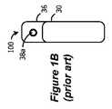
図1A及び図1Bに示すように、SCSシステムは、典型的には、例えば、チタンのような導電材料から形成された生体適合性デバイスケース30を含む「埋込可能パルス発生器(IPG)」100を含む。ケース30は、典型的には、IPGに給電するための回路及びバッテリを保持するが、IPGはまた、外部RFエネルギを通して及びバッテリなしに給電することができる。IPG100は、いくつかの電極106を格納する少なくとも1つの電極アレイ102を含む。電極106は、各電極に結合された個々の電極リード112を同じく収容する可撓性本体108上に担持される。図示の実施形態において、アレイ102上にE1−E8としてラベル付けした8つの電極が存在するが、アレイ及び電極の数は、用途特定であり、従って、変わる可能性がある。アレイ102は、非導電性ヘッダ材料36に固定されて例えばエポキシを含むことができるリードコネクタ38を使用してIPG100に結合する。通信コイル13は、公知のように、患者に対して外部のデバイスからIPG100への及びそこからのデータのテレメトリを可能にする。同じく公知のように、バッテリを外部デバイスから再充電することを可能にするために、追加のコイルが存在する場合がある。As shown in FIGS. 1A and 1B, an SCS system typically includes an “implantable pulse generator (IPG)” that includes a
図2A〜図2Cは、IPG100のようなIPGに使用する典型的なパルスと、パルスを構成するのに使用する回路とを示している。図2Aに示されているのは、電極E1及びE2の間で与えられた振幅(amp)及びパルス幅(pw)の一定電流を送出する2相電流パルスである。各パルスは、複数のパルス位相を含み、周波数fで、ある周期で繰り返される。パルスの振幅、パルス幅、及び周波数は、患者依存であるとすることができ、経験により、すなわち、患者に良好な治療を与えることに基づいて到達することができる。 2A-2C show a typical pulse used in an IPG, such as IPG 100, and circuitry used to construct the pulse. Shown in FIG. 2A is a two-phase current pulse that delivers a constant current of amplitude (amp) and pulse width (pw) provided between electrodes E1 and E2. Each pulse includes a plurality of pulse phases and is repeated at a frequency f with a certain period. The amplitude, pulse width, and frequency of the pulse can be patient dependent and can be reached by experience, that is, based on giving the patient good treatment.
パルスを生成するための回路は、図2Bに示されており、デジタルバス155を通して結合されたタイミングチャネル回路150及び刺激回路160を含む。刺激回路160は、電流ソース(PDAC)83、電流シンク(NDAC)84、スイッチングマトリックス85、及び受動回復スイッチ86を含み、これらの各々は、後で説明する。PDAC83及びNDAC83は、それらがソース又はシンクになるアナログ電流の振幅がデジタル的に制御可能であるので(従って、これらは「デジタル/アナログコンバータ」又はDACである)、かつそれらが典型的にそれぞれPチャネル及びNチャネルトランジスタから作られるのでそのように呼ばれる。 A circuit for generating pulses is shown in FIG. 2B and includes a
図2Aの例示的パルスの治療的に意味のある位相を位相1から始めて最初に以下に説明する。位相1において、電極E1は、電流パルスのカソード又はシンクとして作用するが、電極E2は、電流パルスのアノード又はソースとして作用する。従って、望ましい振幅のソース電流は、スイッチングマトリックス85の適切なスイッチを閉じることによってPDAC83からE2に送出されるが、その同じ振幅のシンク電流は、スイッチングマトリックス85において適切なスイッチを閉じることによってE1からNDAC84の中に引きこまれる。それによって患者の組織(R)を通してE2からE1に電流を流すようにする。位相1中のE1及びE2におけるパルスは、過度の電荷が患者の組織Rに蓄積しないように同じ振幅(反対の極のものであるが)及び同じパルス幅(pw)を有することに注意されたい。 The therapeutically meaningful phase of the exemplary pulse of FIG. 2A is first described below, starting with
パルスは、2相性であるので、位相1の後に最終的に第2の位相(位相2)が続き、第2の位相は、この例においては、2つの電極でのパルスの極性の反転を含む。従って、位相2において、電流がここでは反対方向に組織Rを通して流れるように、E1は、ここではアノードとして、E2は、カソードとして作用する。位相2は、公知のように、それぞれ電極E1及びE2(図2B)に結合された滅結合コンデンサC1及びC2のような電流経路内のいずれかのキャパシタンス上で形成されたかもしれないあらゆる過剰電荷を回復させるのに有用である。滅結合コンデンサC1−CNを電極E1−ENに接続することは、安全手段として作用し、患者の中への直接のDC電流の注入を防止する。しかし、電流の供給中のこのようなコンデンサにわたる電荷の蓄積は、一般的には望ましくない。位相2中にこれらのキャパシタンスを通る電流を逆にすることは、このような蓄積された電荷を能動的に回復することを求めるものであり、従って、位相2は、場合によっては「能動回復」位相と呼ばれる。このように蓄積された電荷を能動的に回復させるために、位相1を通った時と同じ量の電荷が位相2を通ることが好ましく、これは、位相1に等しい位相2の振幅及びパルス幅を作ることによって最も容易に(かつ対称的に)行われる。しかし、位相1及び位相2におけるパルスの間の対称性は、厳密には必要ではないことを当業者は認めるであろう。例えば、位相2におけるより低い振幅及びより長いパルス幅のパルスも、位相1中に通る同じ量の電荷と同等とすることができる。位相2におけるパルスの極性反転は、スイッチングマトリックス85によって達成することができ、スイッチングマトリックス85は、位相2において、E1をPDAC83にかつE2をNDAC84に結合することになる。 Since the pulse is biphasic,
あらゆる蓄積された電荷の完全な回復を保証するために、図2Aに示すように、能動回復位相(位相2)の後に受動回復位相が続く。この受動回復位相において、以前の活性電極E1及びE2に接続された滅結合コンデンサC1−C2は、受動回復スイッチ86(図2B)を通して共通の電位に短絡される。図示の例において、この共通の電位Vbatは、IPG100内のバッテリの電圧を含むが、他の基準電圧を使用することもできる。コンデンサをVbatに短絡することは、患者の組織を通してこれらを実質的に短絡させ、従って、あらゆる蓄積された電荷を釣り合わせて電荷回復を補助する。一部のアーキテクチャは、以前の活性電極のみを、これらの電極に結合された受動回復スイッチ86のみを閉じることによって短絡させることができ、一方、他のアーキテクチャは、電極の全てを受動回復スイッチ86の全てを閉じることによって短絡させることになる。 To ensure complete recovery of any accumulated charge, the active recovery phase (Phase 2) is followed by a passive recovery phase, as shown in FIG. 2A. In this passive recovery phase, the decoupling capacitors C1-C2 connected to the previous active electrodes E1 and E2 are shorted to a common potential through the passive recovery switch 86 (FIG. 2B). In the example shown, this common potential Vbat includes the voltage of the battery in the
各期間における他のパルス位相は、図2Aに示されている。パルス1に先行するのは、プレパルス位相であり、これは、低振幅及び長持続時間のものであり、かつそれに続く位相1パルスとは異なる極性のものである。実験は、このようなプレパルスの使用が、SCS用途においてより深い神経を回復させるのを助けることができることを示唆しているが、このようなプレパルスの使用は、厳密に必要であるということではない。短持続時間の位相1及び2間のinterパルス期間又はパルス間期間は、位相1において刺激された後で神経が安定化することを可能にする。quiet位相又は静的位相が、受動回復位相に続き、かつ本質的にパルス送出の次の期間の前の待機位相として作用する。quiet位相の持続時間は、その期間においてそれに先行する位相の持続時間、並びにその期間が送出する周波数(f)に依存することになる。異なる目的のための他のパルス位相が存在する場合があり、図2Aに示す位相は、単に典型的なものである。 The other pulse phases in each period are shown in FIG. 2A. Preceding
再度図2Bを参照して、各期間の様々な位相は、タイミングチャネル回路150によって制御され、タイミングチャネル回路150は、デジタルバス155を通して刺激回路160の様々な要素をデジタル的に制御する。与えられたIPG100において作動して、恐らくは他の電極上に同時に送出された他のパルスシーケンスを定めるいくつかのタイミングチャネル回路150が存在する可能性がある。しかし、簡単にするために1つのタイミングチャネル回路150のみが示されている。タイミングチャネル回路150は、各パルス期間において様々な位相を定めるのに必要なデータを受信して格納する。このようなパルスパラメータは、デジタルバス115を通して制御回路(例えば、マイクロコントローラ)からタイミングチャネル回路150に提供される。制御回路110は、次に、典型的には、外部コントローラのような外部デバイスから無線でパルスパラメータを受信する。外部コントローラは、典型的には、振幅、パルス幅、周波数のようなパルスパラメータ、使用すべき電極、及びこれらがアノード又はカソードとして作用することになるか否かを選択するように患者又はその臨床医によって使用可能な手持ち式デバイスである。 Referring again to FIG. 2B, the various phases of each period are controlled by the
図2Cは、タイミングチャネル回路150の更なる詳細を示している。図示しているのは、タイマ170及びレジスタバンク180である。タイマ170は、その期間における位相の持続時間(パルス幅)を格納し、一方、レジスタバンク180は、複数の位相について、制御情報、振幅、活性電極、及び電極極性情報を格納する。従って、タイマ170の第1のレジスタは、その期間における第1のパルス位相のパルス幅(図2Aの例のプレパルス(pwpp))を格納し、レジスタバンク180の対応する第1のレジスタは、その制御情報(cntlpp)、振幅(amppp)、活性電極、及び電極極性を格納する。タイマ170の第2のレジスタは、次のパルス位相のパルス幅(位相1(pwp1))を格納し、レジスタバンク180の対応する第2のレジスタは、位相1について、制御情報(cntlp1)、振幅(ampp1)、活性電極、及び電極極性を格納する。その後のパルス位相のためのデータ(inter位相(ip)、位相2(p2)、受動回復(pr)、及びquiet(q))は、タイマ170及びレジスタバンク180に同様に格納される。タイマ170は、一例において状態機械を含むことができる。FIG. 2C shows further details of the
レジスタ(cntlx)内の制御データは、各位相について、刺激回路160の適切な制御に必要な情報を含む。例えば、受動回復位相中に、制御データ(cntlpr)は、ある受動回復スイッチ86を閉じるように命令し、PDAC83及びNDAC84を無効にする。これに対して、能動位相中に、制御データは、受動回復スイッチ86に開くように命令し、PDAC83及びNDAC84を有効にする。The control data in the register (cntlx ) contains information necessary for proper control of the
レジスタバンク180内の各レジスタは、一例において、長さが96ビットであり、最初の16ビットに位相のための制御データ、次の16ビットに指定された位相の振幅、次に、各電極のために8ビットずつを有する。8個の電極ビットの各々は、次に、単一ビットの電極の極性(P)を指定し、残りの7ビットは、その電極が受け入れることになる振幅のパーセント(%)を指定する。従って、プレパルス位相について、E1のための極性ビットPは、電極がアノードとして作用することを指定する「1」であり、従って、指定された振幅(amppp)のソース電流をPDAC83から受け入れる。E1のための残りの7ビットは、E1がプレパルス位相中にソース電流の全体を受け入れることを示す100%をデジタル的に表す。(より複雑な例において、ソース又はシンク電流は、電極間で共有することができ、従って、より小さいパーセントが、これらの電極のための後続の7ビットに示されるであろう。)プレパルス位相中のE2のための極性ビットPは、電極がカソードとして作用することを指定する「0」であり、従って、NDAC84によって制御される時の電流のシンクであることになる。ここでもまた、E2のための残りの7ビットは、E2がプレパルス位相中にシンク電流の全体を受け入れることを示す100%をデジタル的に表す。Each register in
レジスタバンク180内の他のレジスタは、各位相に対して同様にプログラムされる。例えば、レジスタの全てにおけるE3−E8のためのビットの全ては、これらの電極が関与していないので、図2Aの例示的パルス位相に対するゼロに設定される。inter位相に対する振幅(ampip)、受動回復位相に対する振幅(amppr)、及びquiet位相に対する振幅(ampq)は、これらの位相があらゆる電流を能動的に送出するのにPDAC83又はNDAC84を必要としないのでゼロに設定される。The other registers in
タイミングチャネル回路150の目的は、適切な時点にレジスタバンク180内の適切なレジスタから刺激回路160にデータを送ることであり、これは、タイマ170の制御によって行われる。上述したように、様々な位相のためのパルス幅は、タイマ170に格納される。同じくタイマに格納されるのは周波数fであり、その逆数(1/f)は、各期間の持続時間を含む。この期間を知ると、タイマ170は、パルス幅の各々の持続時間を通して循環し、かつレジスタバンク180のデータを適切な時間に刺激回路160に送ることができる。従って、期間の開始時に、タイマ170は、マルチプレクサ190がプレパルスのための第1のレジスタに格納された値をバス155に渡すことを可能にし、バス155は、刺激回路160が電極E1及びE2においてプレパルスを確立することを可能にする。時間pwppが過ぎた後に、タイマ170は、この時点でマルチプレクサ190が、位相1のための第2のレジスタに格納された値を刺激回路160に通し、電極での位相1パルスを確立することを可能にする。他のレジスタは、これらのデータを適切な時間に送るようにタイマ170によって同様に制御される。様々なパルス位相を通して循環するこの処理は継続され、最終的にquiet位相の終わりに、すなわち、pwqの終わりに、タイマ170は、ここでもまたプレパルスデータを有効にし、パルスの新しい期間が確立される。The purpose of the
パルス期間の各位相に従って刺激回路160を制御するためのこの手法は、妥当であるが、本発明者は、この手法もある欠点を有することを見出した。重大な欠点は、より複雑なパルスを定めるためにタイミングチャネル回路150が与える柔軟性の欠如である。例えば、図3に示すパルスを考える。このパルスは、一般的に、図2Aに示すものと同じ位相を含むが、治療的に意味のある位相(位相1及び2)中に指定される電流は、一定電流ではなく、代わりにランプパルスを含む。実験は、ある状況でこのようなランプパルスが治療的に有用である可能性があることを示唆している。しかし、図2Cに示すようなタイミングチャネル回路150は、レジスタバンク180内で一定振幅のみを各位相に対して指定することができるので、このタイプのランプパルスを生成するように刺激回路160に指示することができない。 While this approach for controlling the
本発明者は、図3の電極E1に対する位相1及び2上に重ね合わせて示すような階段状様式でランプを定める一定電流を各々が有する複数のより短い位相にランプパルス位相を分解することにより、図2Cのアーキテクチャを使用してランプパルスを近似することができるであろうと認識している。しかし、これは、その期間内の位相の数の増加を伴うためにレジスタバンク180の拡張を必要とすると考えられる。例えば、適正に滑らかなランプを形成するのに位相1及び2の両方を10のより小さい位相に分解することが必要であろうと仮定する。期間は、次に、24の異なる位相を含むと考えられ、この20の位相は、位相1及び2、プレパルス位相、interパルス位相、受動回復位相、及びquiet位相の各々に必要である。レジスタバンク180は、その期間内で各位相に対してレジスタを含む必要があるので、そのバンク180は、次に、24の異なるレジスタを必要とするであろう。バンク180内の各レジスタに必要な96ビットは、典型的にフリップフロップを含み、従って、この例において、2304(96*24)のフリップフロップ、又はIPG100が更なる数の電極をサポートする場合にはそれよりも多くが必要になると考えられる。集積回路の設計が予め固定され、かつ24未満のレジスタを含む場合に、上で仮定したランプパルスの階段状近似は、容易にその設計において実現することができないであろう。要するに、集積回路設計者は、潜在的に将来の複雑なパルスの設計を取り扱うためにレジスタバンク180に必要以上の数の面積集約型レジスタを提供しなければならないか、又は限定された数のこのようなレジスタを提供し、このような複雑なパルスの使用を控えるかのいずれかであり、いずれの選択肢も望ましくない。The inventor has decomposed the lamp pulse phase into a plurality of shorter phases each having a constant current that defines the lamp in a stepped manner as shown superimposed on
更に、フリップフロップは、刺激回路160が典型的に形成される集積回路上にかなりのレイアウト面積を必要とし、これは、望ましくない。更に、フリップフロップは、それらが計時される時に電力を消費し、これは、節電するためにクロックを開閉する際に複雑性をもたらす可能性がある。過度のレイアウト空間の問題は、上述したように、デバイス内で作動する1つよりも多いタイミングチャネル回路150が存在する場合があるという事実によって悪化する。集積回路の設計が予め固定され、かつ24未満のレジスタを含む場合に、上で仮定したランプパルスの階段状近似は、単純に、その設計で実現することができないであろう。要するに、集積回路設計者は、潜在的に将来の複雑なパルスの設計を取り扱うためにレジスタバンク180に必要以上の数の面積集約型レジスタを提供しなければならないか、又は限定された数のこのようなレジスタを提供し、このような複雑なパルスの使用を控えるかのいずれかであり、いずれの選択肢も望ましくない。 Furthermore, flip-flops require significant layout area on the integrated circuit on which
マルチプレクサ190も、かなりのレイアウト及び制御を取る。マルチプレクサ190は、一般的に、各レジスタから全ての96ビットを受け入れなければならず、従って、図2Cのマルチプレクサ190に入力されている合計576(96*6)のビットが存在する。マルチプレクサ190は、次に、96の選択されたビットの全てを刺激回路160まで駆動しなければならず、これは、システムに電力制約を課す。ここでもまた、1つよりも多いタイミングチャネル回路150がある場合に、このような複雑性及び電力問題が倍増する。
本発明者の意見として同じく残念なことは、パルス内の特定の位相に応じて、レジスタバンク180内のレジスタ値のあるものが必然的に重要でなくなるという事実である。例えば、振幅及び電極値は、図示のinterパルス、受動回復、及びquiet位相に対して必然的にゼロ(又は無関係な値)であることになる。様々な位相の機能が予め既知である場合に、レジスタバンクに必要なフリップフロップの数(及び従ってマルチプレクサ190への入力の総数)は、低減することができると考えられる。例えば、第3のレジスタが、inter位相のためのデータを常に保持することになり、第5のレジスタが、常に受動回復のためのデータを保持することになり、第6のレジスタが、常にquiet位相のためのデータを保持することになることが予め既知である場合に、これらのレジスタは、振幅及び電極値を保持するためのフリップフロップを含む必要はない。しかし、与えられたレジスタ内のフリップフロップの数を低減することは、デバイスの将来の柔軟性を制限する。例えば、上述したばかりのレジスタが仮により小さくされた場合に、これらのレジスタは、将来において能動的刺激相に対して使用することができないであろう。 Also disappointing in my opinion is the fact that certain register values in
従って、より良好な解決法が上述の問題に対して必要であり、かつ本発明の開示によって与えられる。 Therefore, a better solution is needed for the above problem and is provided by the present disclosure.
埋込可能刺激器内の刺激回路を制御するための改良タイミングチャネル回路を開示する。タイミングチャネル回路は、アドレスバスによってアドレス可能なメモリを含む。所望のパルスの様々な位相のためのデータは、一例として、位相内のワードの数を示す指令と、メモリに格納された次の位相のための次のアドレスと、現在の位相のためのパルス幅又は持続時間とを少なくとも含む異なる数のワードを使用してメモリに格納される。現在の位相のためメモリに格納された追加のワードは、刺激回路のための制御データ、パルス振幅、及び電極データを含むことができる。指令データは、アドレスバスを通じて現在の位相内のワードを通してアドレス指定するのに使用され、そのワードは、刺激回路のための制御レジスタにデータバスによって送られ、刺激回路は、データに応じて、電極でのパルス位相を形成することができる。現在の位相のためのパルス幅の持続時間が経過した後に、格納された次のアドレスがアドレスバスに出力され、メモリに格納された次の位相のためのデータにアクセスし、処理を繰り返して次のパルス位相を形成する。メモリは、典型的にはパルス位相の各々のためのデータを格納するのに使用されるレジスタよりも1ビット当たり物理的に小さく、従って、より多数のパルス位相を受け入れることができ、これは、より複雑なパルスの生成を可能にする。各位相について格納されたデータは、一般的に、刺激を必要としない位相のための電極データのような不要なデータは含まず、これは、メモリ内における位相のためのデータのストレージを更に節約する。データは、データバスを通じて1回に1ワードで制御レジスタに順次送られるので、多重化及び制御の複雑性が低減される。 An improved timing channel circuit for controlling a stimulation circuit in an implantable stimulator is disclosed. The timing channel circuit includes a memory addressable by an address bus. The data for the various phases of the desired pulse include, for example, a command indicating the number of words in the phase, the next address for the next phase stored in memory, and the pulse for the current phase. It is stored in memory using a different number of words including at least a width or duration. Additional words stored in memory for the current phase can include control data for the stimulation circuit, pulse amplitude, and electrode data. The command data is used to address through a word in the current phase through the address bus, which word is sent by the data bus to the control register for the stimulus circuit, which in turn responds to the electrode The pulse phase at can be formed. After the duration of the pulse width for the current phase elapses, the next stored address is output to the address bus, accessing the data for the next phase stored in memory, and repeating the process to continue The pulse phase is formed. The memory is typically physically smaller per bit than the register used to store the data for each of the pulse phases, and thus can accept a larger number of pulse phases, Allows generation of more complex pulses. The data stored for each phase generally does not include unnecessary data such as electrode data for phases that do not require stimulation, which further saves storage of data for phases in memory. To do. Since data is sequentially sent to the control register one word at a time through the data bus, multiplexing and control complexity is reduced.
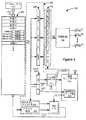
IPG100に対する新しいタイミングチャネル回路200は、図4の最初の例に示されている。様々なパルスパラメータは、例えばランダムアクセスメモリを含むことができるデュアルポートメモリ202に格納される。当業者が理解するように、デュアルポートメモリは、同時に実行することができる2つのデータバス及びアドレスバスとインタフェースで接続することができる。図示のように、バス115は、第1のアドレス/データバスを含み、パルスパラメータは、制御回路110からメモリ202の中にこのバス115を通して書き込まれる。第2のアドレス/データバスは、回路の作動をより良く示すためにデータバス204及びアドレスバス224として別々に示されている。データバス204及びアドレスバス224の基本的な目的は、格納されたパルスパラメータをメモリ202から読み取ること、及びこれらを正しい時間に刺激回路160に送って所望のパルス位相を形成することである。 A new
パルス位相の各々のためのデータは、異なるアドレスでメモリ202にワードで格納され、位相の各々は、その位相の機能に応じて異なる数のワードを含むことができる。図示の例において、各ワードは、32ビットであり、例示的な位相4において、4つのアドレス(addr(x)−addr(x+3))は、その位相のための4つのデータのワード(word1−word4)を保持するように示されている。アドレス指定された時に、これらのワードの各々のためのデータは、データバス204を通してレジスタ208又は210のうちの一方に渡される。具体的には、最初のワード(word1)のためのデータは、レジスタ210に通されるが、その後のワード(word2−word4)のためのデータは、レジスタ206に通される。 The data for each of the pulse phases is stored in words in the
ワードの各々は、各位相について、それらがメモリ202に格納される特定の予め定められたデータ構造及び順序を有する。各位相内の最初のワード(word1)は、指令(cmd)を定める8ビット、次の位相についてのメモリ202内のアドレス(以下で更に説明する「次のアドレス」又はnaddr)を定める8ビット、及び、その位相についてのパルス幅(pw)を含む。各位相内の次のワード(word2)は、刺激回路160の制御(cntl)を定める16ビットと、その位相についてのパルスの振幅(amp)を定める16ビットとを含む。次のワードは、その位相についての電極及びパルスの極性データを含む。すなわち、word3は、電極E1−E4の各々のための8ビットを収容し、各々は、従来技術に関連して上述したように、極性ビットと電極が受け入れる振幅のパーセントを定める7つの後続ビットとを含む。word4は、同じく電極E5−E8についての類似のデータを収容する。 Each of the words has a specific predetermined data structure and order in which they are stored in
各位相のためのデータは、以下のように作動する刺激コントローラ214によってレジスタ206及び210に書き込まれる。各位相内の最初のワードがアドレス指定された時に(例えば、addr(x))、レジスタ210には、指令(cmd)、次のアドレス(naddr)、及びパルス幅(pw)が追加される。次のアドレスnaddrは、次のパルス位相のためのメモリ202内のアドレスを含む次のアドレスレジスタ220に格納される。例えば、位相4のためのデータが現在読み取られていると仮定すると、naddrは、位相5の最初のワードのためのメモリ202内のアドレスを含む。指令データ(cmd)は、刺激コントローラ214に送られる。図5に関してより詳細に以下に説明するように、指令は、様々である可能性がある、その位相について格納されたワードの数を示す。刺激コントローラ214は、このワードの数(216)を決定し、アドレスバス224を通じてメモリ202をアドレス指定するようにマルチプレクサ(mux)218を制御する。例えば、図4の例におけるcmdは、現在の位相が更に3つのワード(word2−word4)から構成されることを刺激コントローラ214に通知するであろう。 Data for each phase is written to
現在のアドレス(addr(x))は、同じく刺激コントローラ214によっても受信されるシステムクロック(Clk)に従って増分又はインクリメントされる(222)。Mux218は、その位相内の残りのワードの全てをアドレス指定するのに必要なだけの回数だけこの増分したアドレスをアドレスバス224に渡す。すなわち、この例におけるMux218は、addr(x+1)−addr(x+3)をメモリ202に渡すように制御され、これは、word2−word4が、システムクロックClkのその後のサイクルにおいてレジスタ206の中に順次ロードされることをもたらす。このようなデータは、ラッチされた状態で、刺激回路160のための制御レジスタ208までユニゾンで通すことができる。レジスタ206及び208はまた、単一回路の中に折り畳むことができる。いずれにしても、その位相内の全てのワードがアドレス指定されてロードされると、刺激コントローラ214は、バス155を通して適切なデータを刺激回路160に出して電極での適切なパルス位相(位相4)を形成するように、制御レジスタ208を有効化する(en)ことができる。バス155を通じて刺激回路160に送られたデータは、従来技術の回路に使用されたものと同じであり(cntl、amp、E1−E8)、その結果、刺激回路160は不変のままであることに注意されたい。 The current address (addr (x)) is incremented or incremented (222) according to the system clock (Clk) also received by the
パルス位相が刺激回路160で確立されると、刺激コントローラ214は、その位相の持続時間が経過するまで更に別のアクションを取るのを待つ。これは、図示の例において、パルス幅カウンタ212の使用により行われ、これはレジスタ210から現在の位相のためのパルス幅(pw)を受信する。システムクロックClkの周期が既知であるので、カウンタ212は、パルス幅の持続時間が満了した時を知ることができ、その時点で、それは、パルス幅終了の指令を刺激コントローラ214に出す。これが起こった時に、刺激コントローラ214は、ここで、既にレジスタ210に格納されていた次のアドレス(naddr)をアドレスバス224に渡すようにMux218を制御する。上述したように、この次のアドレスは、次の位相(位相5)内の最初のワードのアドレスを含む。 Once the pulse phase is established in the
メモリ202が、次の位相(位相5)のこの第1のアドレスを受信した時に、上述の処理を繰り返す。すなわち、次のアドレス(位相6のための)、新しい指令(これは、位相5に対して格納されたワードの数に関して通知する)、及び新しいパルス幅(位相5のための)を含む位相5のための新しいword1が、レジスタ210の中にロードされる。刺激コントローラ214の制御下でMux218は、アドレス増分器222に助けられて位相5内の残りのワードのためのアドレスを提供する。これらの新しいアドレスは、位相5のための適切なデータをレジスタ206にポピュレートし、このデータは、次に、刺激回路160に渡されて位相5のパルスその他を確立する。 When the
システムクロックClkは、典型的に、「メガヘルツ」又はそれよりも速い程度であり、従って、システムクロックの周期(マイクロ秒未満)は、典型的に、種々のパルス位相のパルス幅の持続時間(数10マイクロ秒又はそれよりも長い程度)と比較して短い。その結果、タイミングチャネル回路200は、基本的にメモリ202から刺激回路160にパルスパラメータを瞬時に提供するように機能する。 The system clock Clk is typically on the order of “megahertz” or faster, so the period of the system clock (less than microseconds) is typically the duration (number of pulses) of various pulse phases. Compared to 10 microseconds or longer). As a result, the
図5は、メモリ202の更なる詳細と、図2Aに示す例示的パルスを形成するためにそれをポピュレートすることができる方法とを示している。上述したように、図2Aのパルスは6つの位相を収容し、これら位相の各々のためのデータは、図示のように格納される。PDAC83及びNDAC84にパルス(プレパルス、位相1、及び位相2のような)を発生させることを要求する能動位相は、それらの最初のワード内の指令cmd1により示されている。この指令は、上述したように、アドレス指定を制御することができるように、これらの位相に関連付けられた3つの追加のワードが存在することを刺激コントローラ214に通知する。これら追加のワードは、上述したように、制御データ、振幅、並びに、電極極性及びパーセントを含む。 FIG. 5 shows further details of the
各位相の最初のワードに格納された次のアドレスは、次の位相内の最初のワードを指しており、これは、上述したように刺激コントローラ214がこのような次の位相をアドレス指定することを可能にすることに注意されたい。すなわち、プレパルス位相(addr(1)内)に対して格納された次のアドレスは、位相1の第1のアドレス(addr(5))を指している。位相1(addr(5)内)に対して格納された次のアドレスは、inter位相に対する第1のアドレス(addr(9))を指す等々である。 The next address stored in the first word of each phase points to the first word in the next phase, which means that the
電流の能動的発生ではなく遅延だけを要求するinter位相及びquiet位相のような位相は、それらの最初のワード内の指令cmd0によって示される。このような位相は、刺激回路160に影響を与えないので、それらは、メモリ202に格納され、かつそれらの持続時間及び次のアドレスを含む単に単一ワードとして刺激コントローラ214によって解釈される。 Phases such as the inter phase and quiet phase that require only a delay rather than active generation of current are indicated by the command cmd0 in their first word. Since such phases do not affect the
受動回復位相は、その最初のワード内の指令cmd2により示され、図示の例において2つのワードを必要とする。この位相は、(能動位相のword3及びword4に見出されるような)電極データを必要としないが、受動回復スイッチ86のあるものを閉じるように刺激回路160に通知する制御データ(cntlpr)を必要とする(図2B)。受動回復は、振幅と関連しないので、word2内のそのフィールドは、無関係な値でポピュレートするか、又は単にゼロに設定することができる。The passive recovery phase is indicated by the command cmd2 in its first word and requires two words in the example shown. This phase does not require electrode data (as found in
他の指令(cmd)が可能であるが、図示していない。例えば、他の指令は、刺激中又は刺激のない期間中のいずれかに電極での電圧を測定するように刺激回路160に命令する。このような測定は、インピーダンス測定を行うのに(例えば、電極の連続性を点検するのに)、DAC83及び84(図2B)に対して電源電圧(V+)を設定するのに、又は患者の組織内の電気活動(脳深部刺激用途における発作のような)をモニタするのに有用であり得る。例えば、米国特許第7,444,190号明細書及び第6,993,384号明細書を参照されたい。他の指令は、刺激回路160に電極での電流をバーストさせること、すなわち、パルスを分割してより高い周波数のマイクロパルスにすることによってバーストさせることができる。例えば、米国特許第7,890,182号明細書を参照されたい。そのような他の指令は、刺激回路160のどの態様が制御を必要とするか応じて、メモリ202内に異なる数のワードと異なる制御データ(cntl)とを必要とする。 Other commands (cmd) are possible but not shown. For example, another command instructs the
改良タイミングチャネル回路200の例を理解すると、「背景技術」に説明する従来技術に勝る利点を認めることができる。最初に、メモリ202内のメモリセルは、一般的に、従来技術(180)のレジスタバンク180に使用されるフリップフロップよりも小さく、従って、より多数のメモリ位置を与えてパルスパラメータを保持かつ定義することができる。従って、メモリ202は、より複雑な形状を有するパルスを生成するより大きい柔軟性を提供する。例えば図3のランプパルスを考えてみると、上述したように、これはレジスタバンク180内の必要以上の数のレジスタなしには従来技術で生成するのは実現不可能であった。このようなランプパルスは、図6に示すようにメモリ202内により容易に格納することができ、図6はランプ位相1のパルスのためのデータを示している。ランプパルスは、10msの持続時間にわたって3mAから7.5mAに増加し、従って、1msの10個のより小さい位相(位相1−1から1−10)は、毎回0.5mAだけ振幅を増分される。メモリ202内の増加した数のメモリ位置によって提供される追加の柔軟性は、多くの形状のパルスの提供を可能にする。臨床医は、より良い治療を患者に与えることになるパルス形状を見出す実験を絶えず行っており、従って、このような柔軟性は、そのような実験を可能にする。 Understanding the example of the improved
これに加えて、タイミングチャネル回路200は、パルスパラメータを刺激回路160に経路指定するのに、数百の信号を処理かつ駆動し且つかなりのレイアウト面積及び駆動する電力を使わなければならない個別のマルチプレクサ(図2Cの190)を必要としない。各パルス位相のためのデータは、32ビットワードに分けられるので、データバス204は、図示の例では32ビット幅だけ必要とし、これは、駆動及び制御するのにより容易である。 In addition, the
タイミングチャネル回路200の別の有意な利点は、各位相に対して格納されるデータを低減して無関係な値を排除することができることである。上述したように、従来技術において、全ての位相は、たとえある位相が、interパルス、受動回復、及びquiet位相のための振幅及び電極値のような、レジスタ内の全ての値の使用を必要としなくても、一般的に、レジスタバンク180(図2C)内の完全なレジスタを必要とする(ある専用レジスタが、上述したように短くされていないと仮定すると)。各位相のためのデータをワードに分け、かつ各位相のためのワードの数を定める指令を使用することは、ある位相のためのデータをレジスタバンク180内のレジスタに対して指定された96ビットその他から狭くすることを可能にする。図5に関して上述したように、非能動位相(inter位相、quiet)は、メモリ202に1ワード(32ビット)のみのストレージを必要とし、受動回復は、2ワード(64ビット)を必要とするだけである。このようにして位相データを低減する効率は、更に多い数の電極を有するIPGアーキテクチャにおいてより実質的になる。しかし、厳密にはこのようにして位相データを低減するのではなく、代わりに、全てのパルス位相は、たとえこのデータの一部がある位相に対して有用でなくても、メモリ202に設定数のワードを含むことができる。その状況において、次の位相のためのアドレスは予め既知であり、従って、上述したように、word1に次のアドレスを格納する必要はないであろう。 Another significant advantage of the
開示する回路の利益は、タイミングチャネル回路200が拡張されて1つよりも多いタイミングチャネルをサポートする時に倍増し、4つのタイミングチャネルへの拡張が図7に示されている。図示のように、各々が添字付きで表示されているタイミングチャネル150のためのパルスパラメータの全てを保持するのに1つのメモリ202のみが必要である。ある回路250(図4で点線のボックスで示されている)は、各タイミングチャネルに対して繰り返されるが、制御レジスタ208及び刺激コントローラ214のような他の回路は、各タイミングチャネルによって共有することができる。 The benefits of the disclosed circuit are doubled when the
タイミングチャネル回路200に対して修正を行うことができる。例えば、メモリ202は、制御回路110と通信するバス115と刺激回路160と通信するバス204/224とである2つのアドレス/データバスをサポートするデュアルポートRAMである必要はない。代わりに、単一アドレス/データバス上の通信は、時分割することができると考えられる。これに加えて、データバス204及びアドレスバス224はまた、単一の時分割バスを含むことができるであろう。 Modifications can be made to the
メモリ202は、好ましくは、静的又は動的ランダムアクセスメモリのようなランダムアクセスメモリを含む。しかし、フラッシュメモリのようなプログラマブル/消去可能不揮発性メモリも同様に使用することができると考えられる。パルスパラメータを変更する場合にプログラミング及び消去は追加のコストを必要とするが、そのような治療変更は、高い頻度で起こるわけでなく、消去及び再プログラミングは、患者の観点からは適切に迅速である。
タイミングチャネル回路200は、刺激回路160がその上に通常製作される同じ集積回路に実施することができるが、そこから個別のものとすることもできる。個別の回路ハードウエアブロックとして図4に示すが、回路の態様の多くは、当業者が認めるように同じくソフトウエア又はファームウエアに実施することができる。 The
タイミングチャネル回路200は、多くの異なる方法でスケーリングすることができる。追加の電極は、図示の8つを超えてサポートすることができる。例えば、IPG100が16の電極を収容する場合に、能動位相のような電極データを必要とする各位相に対する追加のワードをメモリ202に含めることができる。あるいは、メモリ202の幅は、例えばより長い64ビットワードを受け入れるように増大させることができる。 The
本発明の特定の実施形態を図示して説明したが、以上の説明は、本発明をそれらの実施形態に限定するように意図していないことを理解しなければならない。本発明の精神及び範囲から逸脱することなく様々な変形及び修正を行うことができることは、当業者に明らかであろう。すなわち、本発明は、特許請求の範囲によって定められるような本発明の精神及び範囲に該当する場合がある代替物、修正物、及び均等物を網羅するように意図している。 While particular embodiments of the present invention have been illustrated and described, it should be understood that the foregoing description is not intended to limit the invention to those embodiments. It will be apparent to those skilled in the art that various modifications and variations can be made without departing from the spirit and scope of the invention. That is, the present invention is intended to cover alternatives, modifications, and equivalents that may fall within the spirit and scope of the present invention as defined by the claims.
110 マイクロコントローラ
160 刺激回路
200 タイミングチャネル回路
212 パルス幅カウンタ
214 刺激コントローラ110
Claims (11)
Translated fromJapanese周期パルスにおける複数のパルス位相を定めるパルスパラメータを格納するためのメモリを含み、前記メモリは、患者の組織を刺激するための電極での前記パルス位相の形成のために前記パルスパラメータを刺激回路にデータバスを通じて提供するようにアドレスバスを通じてアドレス可能であり、
前記パルス位相の各々のための前記パルスパラメータは、前記メモリ内の複数のアドレスに格納され、各パルス位相のための前記複数のアドレスは、そのパルス位相のためのパルスパラメータが格納されたアドレスの数を示す指令を更に含み、
前記メモリから前記指令を受信し、前記指令を格納する第1のレジスタを更に含み、
前記パルスパラメータの少なくとも一部が、第2のレジスタに提供され、
前記第2のレジスタは、前記パルスパラメータの少なくとも一部を前記刺激回路にパラレルに提供する、
ことを特徴とする埋込可能刺激器デバイス。An implantable stimulator device comprising:
A memory for storing a pulse parameter defining a plurality of pulse phases in the periodic pulse, the memory storing the pulse parameter in a stimulation circuit for formation of the pulse phase at an electrode for stimulating a patient's tissue Addressable through the address bus as provided through the data bus,
The pulse parameters for each of the pulse phases are stored at a plurality of addresses in the memory, and the plurality of addresses for each pulse phase is an address of a pulse parameter for that pulse phase. Further includes a command indicating a number;
Receiving said command from said memory, furthersaw including a first register for storing said command,
At least some of the pulse parameters are provided to a second register;
The second register provides at least a portion of the pulse parameter to the stimulation circuit in parallel;
An implantable stimulator device characterized in that.
前記複数のパルス位相の各々のための前記第1のアドレスが、予め定められたデータ構造を含むことを特徴とする請求項1に記載の埋込可能刺激器デバイス。A command indicating the number of addresses is stored in the memory at a first address of the plurality of addresses for each pulse phase;
The implantable stimulator device of claim 1, wherein the first address for each of the plurality of pulse phases includes a predetermined data structure.
前記パルス位相の各々のための前記メモリ内の前記少なくとも1つのアドレスの第1のアドレスから第1のデータを受信するための第1のレジスタと、
前記パルス位相の各々のための前記メモリ内のアドレスが複数存在する場合、前記第1のアドレス以外の他のアドレスから第2のデータを受信するための第2のレジスタと、
前記複数のパルス位相の各々の持続時間を含む前記第1のデータを受信するための制御回路と、
患者の組織を刺激するための電極で前記パルス位相を形成するように刺激回路を構成する前記第2のデータを受信するための前記刺激回路と、
を含むことを特徴とする埋込可能刺激器デバイス。A memory for storing a pulse parameter for defining a plurality of pulse phases in a periodic pulse, wherein the memory for storing the pulse parameter for each of the plurality of pulse phases at at least one address in the memory When,
A first register for receiving first data from a first address of the at least one address in the memory for each of the pulse phases;
A second register for receiving second data from an address other than the first address when there are a plurality of addresses in the memory for each of the pulse phases;
A control circuit for receiving the first data including a duration of each of the plurality of pulse phases;
The stimulation circuit for receiving the second data configuring the stimulation circuit to form the pulse phase with electrodes for stimulating a patient's tissue;
An implantable stimulator device comprising:
Applications Claiming Priority (7)
| Application Number | Priority Date | Filing Date | Title |
|---|---|---|---|
| US201261639814P | 2012-04-27 | 2012-04-27 | |
| US61/639,814 | 2012-04-27 | ||
| US201261654603P | 2012-06-01 | 2012-06-01 | |
| US61/654,603 | 2012-06-01 | ||
| PCT/US2013/033111WO2013162793A1 (en) | 2012-04-27 | 2013-03-20 | Timing channel circuitry for creating pulses in an implantable stimulator device |
| US13/847,676 | 2013-03-20 | ||
| US13/847,676US9008790B2 (en) | 2012-04-27 | 2013-03-20 | Timing channel circuitry for creating pulses in an implantable stimulator device |
Publications (2)
| Publication Number | Publication Date |
|---|---|
| JP2015514550A JP2015514550A (en) | 2015-05-21 |
| JP6070828B2true JP6070828B2 (en) | 2017-02-01 |
Family
ID=49477959
Family Applications (1)
| Application Number | Title | Priority Date | Filing Date |
|---|---|---|---|
| JP2015508976AExpired - Fee RelatedJP6070828B2 (en) | 2012-04-27 | 2013-03-20 | Timing channel circuit for generating pulses in an implantable stimulation device |
Country Status (5)
| Country | Link |
|---|---|
| US (5) | US9008790B2 (en) |
| EP (1) | EP2841152A1 (en) |
| JP (1) | JP6070828B2 (en) |
| AU (1) | AU2013252839B2 (en) |
| WO (1) | WO2013162793A1 (en) |
Families Citing this family (80)
| Publication number | Priority date | Publication date | Assignee | Title |
|---|---|---|---|---|
| US9821159B2 (en) | 2010-11-16 | 2017-11-21 | The Board Of Trustees Of The Leland Stanford Junior University | Stimulation devices and methods |
| WO2012155185A1 (en) | 2011-05-13 | 2012-11-22 | National Ict Australia Ltd | Method and apparatus for measurement of neural response |
| US10588524B2 (en) | 2011-05-13 | 2020-03-17 | Saluda Medical Pty Ltd | Method and apparatus for measurement of neural response |
| US9872990B2 (en) | 2011-05-13 | 2018-01-23 | Saluda Medical Pty Limited | Method and apparatus for application of a neural stimulus |
| CN103648583B (en) | 2011-05-13 | 2016-01-20 | 萨鲁达医疗有限公司 | For measuring method and the instrument of nerves reaction-A |
| WO2012155189A1 (en) | 2011-05-13 | 2012-11-22 | National Ict Australia Ltd | Method and apparatus for estimating neural recruitment - f |
| WO2013111137A2 (en) | 2012-01-26 | 2013-08-01 | Rainbow Medical Ltd. | Wireless neurqstimulatqrs |
| US10206596B2 (en) | 2012-11-06 | 2019-02-19 | Saluda Medical Pty Ltd | Method and system for controlling electrical conditions of tissue |
| EP2908905B1 (en)* | 2012-11-06 | 2020-09-23 | Saluda Medical Pty Limited | System for controlling electrical conditions of tissue |
| WO2014087337A1 (en) | 2012-12-06 | 2014-06-12 | Bluewind Medical Ltd. | Delivery of implantable neurostimulators |
| NZ704579A (en) | 2013-04-19 | 2018-10-26 | Oculeve Inc | Nasal stimulation devices and methods |
| US9433796B2 (en) | 2013-09-03 | 2016-09-06 | Boston Scientific Neuromodulation Corporation | Medical device application for an external device using data logged at an implantable medical device |
| WO2015053769A1 (en)* | 2013-10-09 | 2015-04-16 | Advanced Bionics Ag | Systems for measuring electrode impedance during a normal operation of a cochlear implant system |
| JP6730185B2 (en) | 2013-11-15 | 2020-07-29 | サルーダ・メディカル・ピーティーワイ・リミテッド | Cerebral nerve potential monitoring |
| CA2929874C (en) | 2013-11-22 | 2023-06-13 | Saluda Medical Pty Ltd | Method and device for detecting a neural response in a neural measurement |
| ES2812752T3 (en) | 2014-02-25 | 2021-03-18 | Oculeve Inc | Polymer formulations for nasolacrimal stimulation |
| EP3122247B1 (en) | 2014-03-28 | 2025-05-07 | Saluda Medical Pty Ltd | Assessing neural state from action potentials |
| ES2801348T3 (en) | 2014-05-05 | 2021-01-11 | Saluda Medical Pty Ltd | Improved neurological measurement |
| AU2015292278B2 (en) | 2014-07-25 | 2020-04-09 | Oculeve, Inc. | Stimulation patterns for treating dry eye |
| WO2016011512A1 (en) | 2014-07-25 | 2016-01-28 | Saluda Medical Pty Ltd | Neural stimulation dosing |
| EP3209372B1 (en) | 2014-10-22 | 2020-07-15 | Oculeve, Inc. | Stimulation devices for treating dry eye |
| WO2016065211A1 (en) | 2014-10-22 | 2016-04-28 | Oculeve, Inc. | Contact lens for increasing tear production |
| AU2015349614B2 (en) | 2014-11-17 | 2020-10-22 | Saluda Medical Pty Ltd | Method and device for detecting a neural response in neural measurements |
| WO2016090436A1 (en) | 2014-12-11 | 2016-06-16 | Saluda Medical Pty Ltd | Method and device for feedback control of neural stimulation |
| EP3229890B1 (en) | 2014-12-11 | 2020-05-27 | Saluda Medical Pty Limited | Implantable electrode positioning |
| US10918872B2 (en) | 2015-01-19 | 2021-02-16 | Saluda Medical Pty Ltd | Method and device for neural implant communication |
| US10894158B2 (en) | 2015-04-09 | 2021-01-19 | Saluda Medical Pty Ltd | Electrode to nerve distance estimation |
| WO2016191808A1 (en) | 2015-05-31 | 2016-12-08 | Saluda Medical Pty Ltd | Monitoring brain neural activity |
| CN107614055B (en) | 2015-05-31 | 2022-02-25 | 闭环医疗私人有限公司 | Brain nerve stimulator electrode assembly |
| WO2016191815A1 (en) | 2015-06-01 | 2016-12-08 | Saluda Medical Pty Ltd | Motor fibre neuromodulation |
| US10241148B2 (en)* | 2015-08-11 | 2019-03-26 | Nvidia Corporation | Virtual access of input/output (I/O) for test via an on-chip star network |
| US10105540B2 (en) | 2015-11-09 | 2018-10-23 | Bluewind Medical Ltd. | Optimization of application of current |
| EP3359253A2 (en) | 2015-12-04 | 2018-08-15 | Boston Scientific Neuromodulation Corporation | Systems and methods for sharing therapy paradigms in a neuromodulation system |
| US10391313B2 (en) | 2015-12-04 | 2019-08-27 | Boston Scientific Neuromodulation Corporation | Systems and methods for the development of therapy paradigms for neurological treatments |
| US10252048B2 (en) | 2016-02-19 | 2019-04-09 | Oculeve, Inc. | Nasal stimulation for rhinitis, nasal congestion, and ocular allergies |
| ES2888773T3 (en) | 2016-04-05 | 2022-01-07 | Saluda Medical Pty Ltd | Improved neuromodulation feedback control |
| AU2017260237A1 (en) | 2016-05-02 | 2018-11-22 | Oculeve, Inc. | Intranasal stimulation for treatment of meibomian gland disease and blepharitis |
| EP3474747A4 (en) | 2016-06-24 | 2020-01-22 | Saluda Medical Pty Ltd | NERVOUS STIMULATION FOR REDUCED ARTIFACT |
| US10549091B2 (en) | 2016-09-10 | 2020-02-04 | Boston Scientific Neuromodulation Corporation | Use models for a current generation architecture for an implantable medical device |
| US10589090B2 (en) | 2016-09-10 | 2020-03-17 | Boston Scientific Neuromodulation Corporation | Implantable stimulator device with magnetic field sensing circuit |
| US10716932B2 (en) | 2016-09-10 | 2020-07-21 | Boston Scientific Neuromodulation Corporation | Pulse definition circuitry for creating stimulation waveforms in an implantable pulse generator |
| US11040192B2 (en) | 2016-09-10 | 2021-06-22 | Boston Scientific Neuromodulation Corporation | Current generation architecture for an implantable medical device |
| US10632300B2 (en) | 2016-09-10 | 2020-04-28 | Boston Scientific Neuromodulation Corporation | Measurement circuitry for measuring analog values in an implantable pulse generator |
| US10576265B2 (en) | 2016-09-10 | 2020-03-03 | Boston Scientific Neuromodulation Corporation | Pulse definition circuitry for creating stimulation waveforms in an implantable pulse generator |
| US10716937B2 (en) | 2016-09-10 | 2020-07-21 | Boston Scientific Neuromodulation Corporation | Passive charge recovery circuitry for an implantable medical device |
| US20180071515A1 (en) | 2016-09-10 | 2018-03-15 | Boston Scientific Neuromodulation Corporation | Pulse Definition Circuitry for Creating Stimulation Waveforms in an Implantable Pulse Generator |
| US10786665B2 (en) | 2016-09-10 | 2020-09-29 | Boston Scientific Neuromodulation Corporation | Biasing of a current generation architecture for an implantable medical device |
| US10525252B2 (en) | 2016-09-10 | 2020-01-07 | Boston Scientific Neuromodulation Corporation | Compliance voltage monitoring and adjustment in an implantable medical device |
| US10525253B2 (en) | 2016-10-13 | 2020-01-07 | Boston Scientific Neuromodulation Corporation | Current generation architecture for an implantable medical device including controllable slew rate |
| US10124178B2 (en) | 2016-11-23 | 2018-11-13 | Bluewind Medical Ltd. | Implant and delivery tool therefor |
| US10792491B2 (en) | 2016-11-23 | 2020-10-06 | Boston Scientific Neuromodulation Corporation | Pulsed passive charge recovery circuitry for an implantable medical device |
| WO2018102535A1 (en) | 2016-12-02 | 2018-06-07 | Oculeve, Inc. | Apparatus and method for dry eye forecast and treatment recommendation |
| US20180353764A1 (en) | 2017-06-13 | 2018-12-13 | Bluewind Medical Ltd. | Antenna configuration |
| WO2019032987A1 (en) | 2017-08-11 | 2019-02-14 | Boston Scientific Neuromodulation Corporation | Paresthesia-free spinal cord stimulation system |
| AU2018222994B2 (en) | 2017-09-15 | 2019-11-07 | Boston Scientific Neuromodulation Corporation | Current generation architecture for an implantable stimulator device to promote current steering between electrodes |
| NL2019707B1 (en) | 2017-10-11 | 2019-04-19 | Boston Scient Neuromodulation Corp | Current Generation Architecture for an Implantable Stimulator Device to Promote Current Steering Between Electrodes |
| EP4101500B1 (en) | 2017-09-15 | 2024-10-30 | Boston Scientific Neuromodulation Corporation | Current generation architecture for an implantable stimulator device including distributor circuitry for sending an amplitude-scaled current to digital-to-analog converters at the electrodes |
| US10737100B2 (en) | 2017-11-28 | 2020-08-11 | Medtronic, Inc. | Scalable stimulation waveform scheduler |
| US10926097B2 (en) | 2017-12-15 | 2021-02-23 | Boston Scientific Neuromoduiation Corporation | Use of charge imbalanced pulses in an implantable stimulator to effect a pseudo-constant DC current bias |
| EP4434461A3 (en) | 2018-04-27 | 2025-03-05 | Saluda Medical Pty Ltd | Neurostimulation of mixed nerves |
| EP3755420B1 (en) | 2018-07-03 | 2023-06-28 | Boston Scientific Neuromodulation Corporation | Spinal cord stimulation system with stimulation modes to adapt customized stimulation parameters |
| EP3840822A1 (en) | 2018-08-23 | 2021-06-30 | Boston Scientific Neuromodulation Corporation | Stimulation using long duration waveform phases in a spinal cord stimulator system |
| KR102589640B1 (en) | 2018-12-12 | 2023-10-16 | 삼성전자주식회사 | Converter and circuit device including the same |
| WO2020124142A1 (en)* | 2018-12-17 | 2020-06-25 | Saluda Medical Pty Ltd | Improved neuromodulation implant architecture |
| WO2020162990A2 (en) | 2019-02-08 | 2020-08-13 | Boston Scientific Neuromodulationcorporation | Varying stimulation parameters to prevent tissue habituation in a spinal cord stimulation system |
| CN113423458B (en) | 2019-02-08 | 2024-12-27 | 波士顿科学神经调制公司 | Fitting algorithm for determining optimal stimulation parameters in spinal cord stimulation systems |
| US11565117B2 (en) | 2019-05-02 | 2023-01-31 | Boston Scientific Neuromodulation Corporation | Amplitude modulating waveform pattern generation for stimulation in an implantable pulse generator |
| CA3143251C (en) | 2019-07-02 | 2024-06-18 | Boston Scientific Neuromodulation Corporation | Spinal cord stimulation system determining optimal sub-perception therapy by using neural dose |
| EP3993867B1 (en) | 2019-09-06 | 2024-10-30 | Boston Scientific Neuromodulation Corporation | Management of compliance voltage for a stimulator device |
| EP4616898A2 (en) | 2020-01-09 | 2025-09-17 | Boston Scientific Neuromodulation Corporation | External controller for controlling sub-perception stimulation |
| WO2021151095A1 (en) | 2020-01-25 | 2021-07-29 | Nevro Corp. | Systems and methods for direct suppression of nerve cells |
| US20230128146A1 (en) | 2020-03-06 | 2023-04-27 | Boston Scientific Neuromodulation Corporation | Varying Optimal Sub-Perception Stimulation as a Function of Time Using a Modulation Function |
| US11426588B2 (en) | 2020-04-22 | 2022-08-30 | Advanced Neuromodulation Systems, Inc. | Systems and methods for arbitrary current waveform generation |
| US11478644B2 (en) | 2020-04-22 | 2022-10-25 | Advanced Neuromodulation Systems, Inc. | Systems and methods for DC protection in implantable pulse generators |
| US20220161033A1 (en) | 2020-11-20 | 2022-05-26 | Boston Scientific Neuromodulation Corporation | Compliance Voltage Monitoring and Adjustment in an Implantable Medical Device Using Low Side Sensing |
| US12364867B2 (en) | 2020-12-30 | 2025-07-22 | Advanced Neuromodulation Systems, Inc. | System and method for operating an implantable pulse generator for neuromodulation |
| WO2022217184A1 (en) | 2021-04-06 | 2022-10-13 | Boston Scientific Neuromodulation Corporation | Current generation architecture for an implantable stimulator device |
| US12133981B2 (en) | 2021-06-11 | 2024-11-05 | Nevro Corp. | Neurostimulation waveforms having a base component and a high frequency component, and associated systems and methods |
| US12005257B2 (en) | 2021-08-18 | 2024-06-11 | Advanced Neuromodulation Systems, Inc. | Neuromodulation therapy with custom instruction set architecture for a stimulation engine system |
| US11400299B1 (en) | 2021-09-14 | 2022-08-02 | Rainbow Medical Ltd. | Flexible antenna for stimulator |
Family Cites Families (26)
| Publication number | Priority date | Publication date | Assignee | Title |
|---|---|---|---|---|
| US4407288B1 (en)* | 1981-02-18 | 2000-09-19 | Mieczyslaw Mirowski | Implantable heart stimulator and stimulation method |
| US4690145A (en)* | 1985-06-17 | 1987-09-01 | Minnesota Mining And Manufacturing Company | Output limited electrical stimulator for biological tissue |
| US5603726A (en)* | 1989-09-22 | 1997-02-18 | Alfred E. Mann Foundation For Scientific Research | Multichannel cochlear implant system including wearable speech processor |
| US6516227B1 (en) | 1999-07-27 | 2003-02-04 | Advanced Bionics Corporation | Rechargeable spinal cord stimulator system |
| US6993384B2 (en) | 2001-12-04 | 2006-01-31 | Advanced Bionics Corporation | Apparatus and method for determining the relative position and orientation of neurostimulation leads |
| US7689276B2 (en) | 2002-09-13 | 2010-03-30 | Leptos Biomedical, Inc. | Dynamic nerve stimulation for treatment of disorders |
| US7483748B2 (en) | 2002-04-26 | 2009-01-27 | Medtronic, Inc. | Programmable waveform pulses for an implantable medical device |
| US7024246B2 (en) | 2002-04-26 | 2006-04-04 | Medtronic, Inc | Automatic waveform output adjustment for an implantable medical device |
| ES2426255T3 (en) | 2002-06-28 | 2013-10-22 | Boston Scientific Neuromodulation Corporation | Microstimulator that has a built-in power source and a two-way telemetry system |
| US7539538B2 (en) | 2004-05-28 | 2009-05-26 | Boston Science Neuromodulation Corporation | Low power loss current digital-to-analog converter used in an implantable pulse generator |
| AT7710U3 (en) | 2004-06-30 | 2006-07-15 | Avl List Gmbh | METHOD FOR CREATING A MODEL OF A CONTROL SIZE FOR NONLINEAR, STATIONARY REAL SYSTEMS, FOR EXAMPLE, COMBUSTION ENGINES OR SUBSYSTEMS THEREOF |
| US20060173493A1 (en)* | 2005-01-28 | 2006-08-03 | Cyberonics, Inc. | Multi-phasic signal for stimulation by an implantable device |
| US8620436B2 (en) | 2005-07-08 | 2013-12-31 | Boston Scientific Neuromodulation Corporation | Current generation architecture for an implantable stimulator device having coarse and fine current control |
| US7444181B2 (en) | 2005-12-14 | 2008-10-28 | Boston Scientific Neuromodulation Corporation | Techniques for sensing and adjusting a compliance voltage in an implantable stimulator device |
| US8649858B2 (en) | 2007-06-25 | 2014-02-11 | Boston Scientific Neuromodulation Corporation | Architectures for an implantable medical device system |
| US8131377B2 (en) | 2007-07-11 | 2012-03-06 | Boston Scientific Neuromodulation Corporation | Telemetry listening window management for an implantable medical device |
| US20090024184A1 (en) | 2007-07-17 | 2009-01-22 | Nurotron Biotechnology, Inc. | Cochlear implant utilizing multiple-resolution current sources and flexible data encoding |
| US7890182B2 (en) | 2008-05-15 | 2011-02-15 | Boston Scientific Neuromodulation Corporation | Current steering for an implantable stimulator device involving fractionalized stimulation pulses |
| FR2940458B1 (en) | 2008-12-24 | 2011-03-04 | Commissariat Energie Atomique | DEVICE AND METHOD FOR CHARACTERIZATION OF ELECTRIC OR ELECTRONIC COMPONENTS. |
| US9233254B2 (en) | 2009-02-17 | 2016-01-12 | Boston Scientific Neuromodulation Corporation | Selectable boost converter and charge pump for compliance voltage generation in an implantable stimulator device |
| US20100331921A1 (en)* | 2009-06-24 | 2010-12-30 | Pacesetter, Inc. | Neurostimulation device and methods for controlling same |
| JP5802218B2 (en)* | 2009-12-30 | 2015-10-28 | ボストン サイエンティフィック ニューロモデュレイション コーポレイション | System and method for independently operating multiple neural stimulation channels |
| US8099170B2 (en)* | 2010-03-19 | 2012-01-17 | Medtronic, Inc. | Electrical stimulation based on phase response mapping |
| US8768453B2 (en)* | 2010-10-13 | 2014-07-01 | Boston Scientific Neuromodulation Corporation | Monitoring electrode voltages in an implantable medical device system having daisy-chained electrode-driver integrated circuits |
| EP2627404B1 (en) | 2010-10-13 | 2017-12-13 | Boston Scientific Neuromodulation Corporation | Architectures for an implantable medical device system having daisy-chained electrode-drive integrated circuits |
| US9061140B2 (en)* | 2010-10-13 | 2015-06-23 | Boston Scientific Neuromodulation Corporation | Sample and hold circuitry for monitoring voltages in an implantable neurostimulator |
- 2013
- 2013-03-20JPJP2015508976Apatent/JP6070828B2/ennot_activeExpired - Fee Related
- 2013-03-20EPEP13714461.4Apatent/EP2841152A1/ennot_activeWithdrawn
- 2013-03-20WOPCT/US2013/033111patent/WO2013162793A1/enactiveApplication Filing
- 2013-03-20AUAU2013252839Apatent/AU2013252839B2/enactiveActive
- 2013-03-20USUS13/847,676patent/US9008790B2/enactiveActive
- 2015
- 2015-03-03USUS14/636,380patent/US9144687B2/enactiveActive
- 2015-09-18USUS14/858,554patent/US9468771B2/enactiveActive
- 2016
- 2016-10-10USUS15/289,809patent/US9925385B2/enactiveActive
- 2018
- 2018-02-14USUS15/896,991patent/US10391322B2/enactiveActive
Also Published As
| Publication number | Publication date |
|---|---|
| US20150174419A1 (en) | 2015-06-25 |
| AU2013252839A1 (en) | 2014-11-13 |
| US9925385B2 (en) | 2018-03-27 |
| WO2013162793A1 (en) | 2013-10-31 |
| US20160008611A1 (en) | 2016-01-14 |
| US20180169424A1 (en) | 2018-06-21 |
| US20170021181A1 (en) | 2017-01-26 |
| US10391322B2 (en) | 2019-08-27 |
| US9468771B2 (en) | 2016-10-18 |
| AU2013252839B2 (en) | 2015-09-17 |
| JP2015514550A (en) | 2015-05-21 |
| US20130289661A1 (en) | 2013-10-31 |
| EP2841152A1 (en) | 2015-03-04 |
| US9008790B2 (en) | 2015-04-14 |
| US9144687B2 (en) | 2015-09-29 |
Similar Documents
| Publication | Publication Date | Title |
|---|---|---|
| JP6070828B2 (en) | Timing channel circuit for generating pulses in an implantable stimulation device | |
| US12128234B2 (en) | Passive charge recovery circuitry for an implantable medical device | |
| US12023482B2 (en) | Compliance voltage monitoring and adjustment in an implantable medical device | |
| JP6242410B2 (en) | Architecture for sharing the current source of implantable medical devices | |
| JP5969500B2 (en) | Direct memory access (DMA) control stimulus | |
| CN104582790B (en) | Therapy Delivery Architecture for Implantable Medical Devices |
Legal Events
| Date | Code | Title | Description |
|---|---|---|---|
| A521 | Request for written amendment filed | Free format text:JAPANESE INTERMEDIATE CODE: A523 Effective date:20141226 | |
| A621 | Written request for application examination | Free format text:JAPANESE INTERMEDIATE CODE: A621 Effective date:20141226 | |
| A977 | Report on retrieval | Free format text:JAPANESE INTERMEDIATE CODE: A971007 Effective date:20151113 | |
| A131 | Notification of reasons for refusal | Free format text:JAPANESE INTERMEDIATE CODE: A131 Effective date:20151116 | |
| A521 | Request for written amendment filed | Free format text:JAPANESE INTERMEDIATE CODE: A523 Effective date:20160216 | |
| A131 | Notification of reasons for refusal | Free format text:JAPANESE INTERMEDIATE CODE: A131 Effective date:20160425 | |
| A521 | Request for written amendment filed | Free format text:JAPANESE INTERMEDIATE CODE: A523 Effective date:20160722 | |
| TRDD | Decision of grant or rejection written | ||
| A01 | Written decision to grant a patent or to grant a registration (utility model) | Free format text:JAPANESE INTERMEDIATE CODE: A01 Effective date:20161212 | |
| A61 | First payment of annual fees (during grant procedure) | Free format text:JAPANESE INTERMEDIATE CODE: A61 Effective date:20161219 | |
| R150 | Certificate of patent or registration of utility model | Ref document number:6070828 Country of ref document:JP Free format text:JAPANESE INTERMEDIATE CODE: R150 | |
| R250 | Receipt of annual fees | Free format text:JAPANESE INTERMEDIATE CODE: R250 | |
| LAPS | Cancellation because of no payment of annual fees |