JP6065721B2 - Drive circuit, semiconductor integrated circuit, and drive circuit control method - Google Patents
Drive circuit, semiconductor integrated circuit, and drive circuit control methodDownload PDFInfo
- Publication number
- JP6065721B2 JP6065721B2JP2013080261AJP2013080261AJP6065721B2JP 6065721 B2JP6065721 B2JP 6065721B2JP 2013080261 AJP2013080261 AJP 2013080261AJP 2013080261 AJP2013080261 AJP 2013080261AJP 6065721 B2JP6065721 B2JP 6065721B2
- Authority
- JP
- Japan
- Prior art keywords
- switching element
- voltage
- transistor
- drive circuit
- turned
- Prior art date
- Legal status (The legal status is an assumption and is not a legal conclusion. Google has not performed a legal analysis and makes no representation as to the accuracy of the status listed.)
- Expired - Fee Related
Links
- 239000004065semiconductorSubstances0.000titleclaimsdescription23
- 238000000034methodMethods0.000titleclaimsdescription9
- 230000004044responseEffects0.000claimsdescription11
- 238000001514detection methodMethods0.000description10
- 150000001875compoundsChemical class0.000description8
- 238000005516engineering processMethods0.000description7
- 239000000758substrateSubstances0.000description7
- 230000007423decreaseEffects0.000description6
- 238000010586diagramMethods0.000description6
- 239000003990capacitorSubstances0.000description5
- 230000003071parasitic effectEffects0.000description5
- 230000002093peripheral effectEffects0.000description5
- JMASRVWKEDWRBT-UHFFFAOYSA-NGallium nitrideChemical compound[Ga]#NJMASRVWKEDWRBT-UHFFFAOYSA-N0.000description4
- HBMJWWWQQXIZIP-UHFFFAOYSA-Nsilicon carbideChemical compound[Si+]#[C-]HBMJWWWQQXIZIP-UHFFFAOYSA-N0.000description4
- XUIMIQQOPSSXEZ-UHFFFAOYSA-NSiliconChemical compound[Si]XUIMIQQOPSSXEZ-UHFFFAOYSA-N0.000description3
- 239000002131composite materialSubstances0.000description3
- 230000005669field effectEffects0.000description3
- 229910052710siliconInorganic materials0.000description3
- 239000010703siliconSubstances0.000description3
- 229910002601GaNInorganic materials0.000description2
- 230000000295complement effectEffects0.000description2
- 229910010271silicon carbideInorganic materials0.000description2
- 230000004888barrier functionEffects0.000description1
- 230000000694effectsEffects0.000description1
- 238000009499grossingMethods0.000description1
- 230000007246mechanismEffects0.000description1
- 229910044991metal oxideInorganic materials0.000description1
- 150000004706metal oxidesChemical class0.000description1
- 230000008569processEffects0.000description1
- 230000001172regenerating effectEffects0.000description1
- 238000004804windingMethods0.000description1
Images


Classifications
- H—ELECTRICITY
- H03—ELECTRONIC CIRCUITRY
- H03K—PULSE TECHNIQUE
- H03K19/00—Logic circuits, i.e. having at least two inputs acting on one output; Inverting circuits
- H03K19/0008—Arrangements for reducing power consumption
- H03K19/0019—Arrangements for reducing power consumption by energy recovery or adiabatic operation
- H—ELECTRICITY
- H03—ELECTRONIC CIRCUITRY
- H03K—PULSE TECHNIQUE
- H03K17/00—Electronic switching or gating, i.e. not by contact-making and –breaking
- H03K17/08—Modifications for protecting switching circuit against overcurrent or overvoltage
- H03K17/081—Modifications for protecting switching circuit against overcurrent or overvoltage without feedback from the output circuit to the control circuit
- H03K17/0812—Modifications for protecting switching circuit against overcurrent or overvoltage without feedback from the output circuit to the control circuit by measures taken in the control circuit
- H03K17/08122—Modifications for protecting switching circuit against overcurrent or overvoltage without feedback from the output circuit to the control circuit by measures taken in the control circuit in field-effect transistor switches
- H—ELECTRICITY
- H03—ELECTRONIC CIRCUITRY
- H03K—PULSE TECHNIQUE
- H03K2217/00—Indexing scheme related to electronic switching or gating, i.e. not by contact-making or -breaking covered by H03K17/00
- H03K2217/0081—Power supply means, e.g. to the switch driver
Landscapes
- Physics & Mathematics (AREA)
- Engineering & Computer Science (AREA)
- Computer Hardware Design (AREA)
- Computing Systems (AREA)
- General Engineering & Computer Science (AREA)
- Mathematical Physics (AREA)
- Electronic Switches (AREA)
- Power Conversion In General (AREA)
Description
Translated fromJapanese開示する技術は、駆動回路、半導体集積回路、及び駆動回路の制御方法に関する。 The disclosed technology relates to a drive circuit, a semiconductor integrated circuit, and a control method of the drive circuit.
化合物半導体には、窒化ガリウム(GaN)などIII−V族化合物半導体、及び炭化珪素(SiC)などIV−IV族化合物半導体等がある。化合物半導体を用いたスイッチング素子には、負のゲート電圧が印加されていない場合にドレイン電流が流れ、負のゲート電圧が印加されることでドレイン電流が遮断されるノーマリーオン形がある。 Compound semiconductors include III-V group compound semiconductors such as gallium nitride (GaN), and IV-IV group compound semiconductors such as silicon carbide (SiC). A switching element using a compound semiconductor has a normally-on type in which a drain current flows when a negative gate voltage is not applied, and the drain current is cut off when a negative gate voltage is applied.
しきい値電圧が負のFET(Field Effect Transistor)を用いた反転増幅器には、しきい値電圧が負のFETとしきい値電圧が正のFETとにより直列回路を形成した反転増幅回路がある。この反転増幅回路では、しきい値電圧が負のFETの低圧側にしきい値電圧が正のFETを接続し、各々のFETのゲートの入力電圧を上昇させることで、各々のFETをオンする。また、入力電圧を0vとすることで、しきい値が正のFETがオフする。これにより、均圧用抵抗によりしきい値電圧が負のFETのソース電位が上昇し、しきい値電圧が負のFETがオフするようにしている。 An inverting amplifier using an FET (Field Effect Transistor) having a negative threshold voltage includes an inverting amplifier circuit in which a series circuit is formed by an FET having a negative threshold voltage and an FET having a positive threshold voltage. In this inverting amplifier circuit, an FET having a positive threshold voltage is connected to a low voltage side of an FET having a negative threshold voltage, and each FET is turned on by raising the input voltage of the gate of each FET. Further, by setting the input voltage to 0 v, the FET having a positive threshold value is turned off. As a result, the source potential of the FET having a negative threshold voltage is increased by the voltage equalizing resistor, and the FET having a negative threshold voltage is turned off.
ノーマリーオン形スイッチング素子とノーマリーオフ形スイッチング素子をカスコード接続した複合型半導体装置がある。この複合型半導体装置では、ノーマリーオン形スイッチング素子のゲートをノーマリーオフ形スイッチング素子のソースに接続し、ノーマリーオフ形スイッチング素子のゲート信号により、ノーマリーオフ動作させる。 There is a composite type semiconductor device in which a normally-on type switching element and a normally-off type switching element are cascode-connected. In this composite semiconductor device, the gate of the normally-on type switching element is connected to the source of the normally-off type switching element, and the normally-off type switching device is normally turned off by the gate signal of the normally-off type switching element.
ところで、高電圧電源のスイッチングに用いる所謂パワートランジスタ等のスイッチング素子は、所定のパッケージ内に形成され、パッケージに形成したリードが基板等に接続される。リードなどの配線には、少なからず寄生インダクタンスがある。このため、ノーマリーオン形スイッチング素子の駆動回路では、ノーマリーオフ形スイッチング素子をオフしたとき、ノーマリーオフ形スイッチング素子のドレイン−ソース間に過電圧が生じることがある。 Incidentally, a switching element such as a so-called power transistor used for switching of a high voltage power source is formed in a predetermined package, and a lead formed in the package is connected to a substrate or the like. Wiring such as leads has a considerable parasitic inductance. For this reason, in a normally-on type switching element drive circuit, when the normally-off type switching element is turned off, an overvoltage may be generated between the drain and source of the normally-off type switching element.
ここから、複合型半導体装置では、ノーマリーオフ形スイッチング素子のドレイン−ゲート間、又はドレイン−ソース間に、ツェナーダイオード或いはコンデンサを用いた電圧クランプ手段を設けている。 Thus, in the composite semiconductor device, voltage clamping means using a Zener diode or a capacitor is provided between the drain and gate of the normally-off switching element or between the drain and source.
しかしながら、電圧クランプ手段として用いるツェナーダイオード等は、過電圧分の電力を消費することで、過電圧を抑制している。 However, a Zener diode or the like used as a voltage clamping means suppresses overvoltage by consuming power corresponding to the overvoltage.
開示の技術は、一つの側面として、大容量のスイッチング素子を駆動する際に生じる過電圧の効率的な抑制を図るものである。 As one aspect, the disclosed technology aims to efficiently suppress an overvoltage generated when a large-capacity switching element is driven.
開示の技術は、 第1のスイッチング素子のソースに直列に接続される第2のスイッチング素子を含む。第2のスイッチング素子は、前記第1のスイッチング素子がオンされるときにオンされ、前記第1のスイッチング素子がオフされるときにオフされる。 The disclosed technique includes a second switching element connected in series to the source of the first switching element. The second switching element is turned on when the first switching element is turned on, and is turned off when the first switching element is turned off.
通電素子は、前記第2のスイッチング素子のドレインと電源ラインとの間に設けられ、前記第2のスイッチング素子をオフさせる信号に応じて、前記第2のスイッチング素子のドレインを前記電源ラインに接続する。 The energization element is provided between the drain of the second switching element and the power supply line, and connects the drain of the second switching element to the power supply line in response to a signal for turning off the second switching element. To do.
開示の技術は、一つの側面として、第2のスイッチング素子のドレインに生じる過電圧の電力を電源ラインに回生することで、電力の使用効率の向上を図る、という効果を有する。 As one aspect, the disclosed technique has an effect of improving the power use efficiency by regenerating the overvoltage power generated in the drain of the second switching element to the power supply line.
以下、図面を参照して開示する技術の実施の形態の一例を詳細に説明する。
〔第1の実施形態〕Hereinafter, an example of an embodiment of the technology disclosed will be described in detail with reference to the drawings.
[First Embodiment]
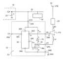
図1には、第1の実施形態に係る駆動回路10を示している。駆動回路10は、集積回路(integrated circuit)12に形成される。駆動回路10は、パワートランジスタPTrの駆動に用いられる。駆動回路10は、第1の実施形態において駆動回路として機能し、集積回路12は、第1の実施形態において半導体集積回路の一例として機能する。また、パワートトランジスタPTrは、第1の実施形態において第1のスイッチング素子の一例として機能する。 FIG. 1 shows a
集積回路12は、例えば、基板14に取り付けられる。基板14には、所定電圧(例えば5v、以下、電圧VCCとする)の直流電力を出力する直流電源部16が設けられる。また、基板14には、電圧VCCの電力により動作する各種の機能回路(以下、周辺回路とする)18が設けられている。周辺回路18は、電源配線(以下、電源ラインとする)20を介して直流電源部16に接続され、直流電源部16から電圧VCCの電力が供給されて動作する。 The
なお、集積回路12は、複数の駆動回路10を含んでも良い。また、集積回路12は、直流電源部16を含み、外部から供給される所定電圧の直流電力を、直流電源16により駆動回路10の動作電圧(電圧VCC)に変換しても良い。更に、集積回路12は、複数の周辺回路18を含んでも良い。 The
直流電源部16は、所定の静電容量Cのコンデンサ22を含む一般的機構の電源回路が適用される。コンデンサ22は、一端が電源ライン20に接続され、他端が接地され、直流電源部16から電源ライン20へ出力する電圧VCCの平滑化を図る機能を備える。 As the DC
集積回路12に設けられる駆動回路10は、電源端子24A、及び接地端子24Bを備える。駆動回路10は、電源端子24Aが電源ライン20に接続され、接地端子24Bが接地(GND)されている。 The
また、駆動回路10は、入力端子26A、出力端子26B、及び出力端子26Cを備える。なお、電源端子24A、接地端子24B、入力端子26A、及び出力端子26B、26Cは、集積回路12の端子としても機能する。 The
第1の実施形態では、一例としてN型のパワートランジスタPTrを用いている。また、第1の実施形態では、パワートランジスタPTrをノーマリーオン形(normally on type)としている。駆動回路10には、パワートランジスタPTrが接続される。パワートランジスタPTrは、ゲートGが駆動回路10の出力端子26Bに接続され、低圧側電極であるソースSが駆動回路10の出力端子26Cに接続されている。また、駆動回路10には、パワートランジスタPTrをスイッチング駆動するための駆動信号Cinが入力端子26Aに入力される。 In the first embodiment, an N-type power transistor PTr is used as an example. In the first embodiment, the power transistor PTr is normally on type. A power transistor PTr is connected to the
パワートランジスタPTrは、高圧側電極であるドレインDに負荷28が接続されている。負荷28は、電圧VCCと比較して高い所定電圧(例えば百数十vから数百vの予め設定された電圧、以下、電圧VINとする)の電源ライン30に接続されている。駆動回路10は、パワートランジスタPTrをスイッチング動作することで、負荷28への電力供給を断続する。 In the power transistor PTr, a
負荷28としては、例えば変圧器が用いられる。パワートランジスタPTrがオンすることにより負荷28にはドレイン電流IDが流れ(オン)、パワートランジスタPTrがオフすることでドレイン電流IDが止まる(オフ)。負荷28は、ドレイン電流IDがオン・オフされることで、一次側に供給される電圧VIN及び巻線比に応じた電圧を二次側から出力する。従って、負荷28として変圧器を用いた場合、駆動回路10及びパワートランジスタPTrは、高電圧電源回路の一部として機能する。 For example, a transformer is used as the
なお、パワートランジスタPTrは、任意の機能の負荷28を適用することができる。駆動回路10及びパワートランジスタPTrは、負荷28に応じて例えば高電圧用のインバータ回路、及び大出力信号用の増幅回路等の一部として機能し得る。また、パワートランジスタPTrは、電源VINの電圧に応じた耐電圧となっている。 Note that a
ノーマリーオン形のパワートランジスタPTrとしては、各種の化合物半導体を用いたトランジスタが適用される。例えば、パワートランジスタPTrとしては、III−V族化合物半導体である窒化ガリウム(GaN)を用いた窒化ガリウム高電子移動度トランジスタ(GaN HEMT:GaN High Electron Mobility Transistor )が適用される。また、パワートランジスタPTrは、IV−IV族化合物半導体である炭化珪素(SiC)を用いた炭化珪素接合電界効果トランジスタ(SiC JFET:SiC Junction field effect transistor)等が適用される。なお、パワートランジスタPTrは、化合物半導体に限るものではなく、BJT(Bipolar junction transistor)であっても良い。また、パワートランジスタPTrは、MOSFET(metal oxide silicon field effect transistor)であっても良く、IGBT(Insulated Gate Bipolar Transistor)であっても良い。 As the normally-on type power transistor PTr, transistors using various compound semiconductors are applied. For example, as the power transistor PTr, a GaN high electron mobility transistor (GaN HEMT) using gallium nitride (GaN) which is a group III-V compound semiconductor is applied. As the power transistor PTr, a silicon carbide junction field effect transistor (SiC JFET) using silicon carbide (SiC) which is an IV-IV group compound semiconductor is used. The power transistor PTr is not limited to a compound semiconductor, and may be a BJT (bipolar junction transistor). The power transistor PTr may be a MOSFET (metal oxide silicon field effect transistor) or an IGBT (Insulated Gate Bipolar Transistor).
図2には、パワートランジスタPTrの一例を示す。パワートランジスタPTrは、例えば、TO-3Pなどの所定のパッケージ32内に形成されている。パッケージ32には、ドレインD、ソースS、及びゲートGの各々に対応する複数のリード34が形成されている。パワートランジスタPTrは、パッケージ32を基板14等に固定することで取り付けられ、各リード34が基板14上の配線パターンや集積回路12の端子にワイヤボンディング等により接続される。リード34は、第1の実施形態において配線の一部として機能する。なお、パワートランジスタPTrは、TO−3Pのパッケージ32に限らず、任意のパッケージに形成されたものが適用される。 FIG. 2 shows an example of the power transistor PTr. The power transistor PTr is formed in a
図1に示すように、駆動回路10は、コントロール回路36を備える。コントロール回路36は、電源端子38A、及び接地端子38Bを備えている。コントロール回路36は、電源端子38Aが駆動回路10の電源端子24Aに接続され、接地端子38Bが、駆動回路10の接地端子24Bに接続され、電源端子24Aに入力される電圧VCCにより動作する。 As shown in FIG. 1, the
コントロール回路36は、入力端子38C、及び出力端子38D、38Eを備える。コントロール回路36は、入力端子38Cが駆動回路10の入力端子26Aに接続されている。また、コントロール回路36は、出力端子38Dが駆動回路10の出力端子26Bに接続されている。 The
コントロール回路36は、入力端子38Cから入力される駆動信号Cinに応じた電圧(以下、制御電圧Vcとする)を出力端子26Bから出力することで、パワートランジスタPTrのゲートGの電位(以下、ゲート電圧VGとする)を制御する。 The
駆動回路10には、トランジスタMaが設けられている。トランジスタMaは、第1の実施形態において第2のスイッチング素子として機能する。トランジスタMaは、N形MOSFETで、かつ、ノーマリーオフ(normally off type)形となっている。 The
トランジスタMaは、ソースSが駆動回路10に設けている接地端子24Bに接続されている。また、トランジスタMaは、ドレインDがノード40に接続され、このノード40が駆動回路10の出力端子26Cに接続されている。駆動回路10は、ノーマリーオン形のパワートランジスタPTrの低圧側にノーマリーオフ形のトランジスタMaが所謂カスコード接続されている。 The transistor Ma has a source S connected to a ground terminal 24 </ b> B provided in the
また、トランジスタMaは、ゲートGがコントロール回路36の出力端子38Eに接続されている。コントロール回路36は、トランジスタMaをオン・オフ駆動する制御信号Csを出力端子38Eから出力する。駆動回路10は、コントロール回路36から出力する制御信号CsによりトランジスタMaを駆動して、パワートランジスタPTrのソースSの電位(以下、ソース電圧VSとする)を制御する。 The transistor Ma has a gate G connected to the
ノーマリーオン形のパワートランジスタPTrは、ゲートGのしきい値電圧Vthが負となっている。以下、負のしきい値電圧を、−Vthと表記する(−Vth<0v、例えば、−Vth=−1.0v)。ノーマリーオン形のパワートランジスタPTrは、例えば、ソースSの電圧VSが0vの場合、ゲートGの電圧VGが0v以上ではオン状態となる。また、ノーマリーオン形のパワートランジスタPTrは、ゲート電圧VGがしきい値電圧−Vthより低くなる(VG<−Vth<0v)ことでオフする。 In the normally-on type power transistor PTr, the threshold voltage Vth of the gate G is negative. Hereinafter, the negative threshold voltage is expressed as −Vth (−Vth <0 v, for example, −Vth = −1.0 v). For example, when the voltage VS of the source S is 0v, the normally-on type power transistor PTr is turned on when the voltage VG of the gate G is 0v or more. Further, the normally-on type power transistor PTr is turned off when the gate voltage VG becomes lower than the threshold voltage −Vth (VG <−Vth <0v).
すなわち、ノーマリーオン形のパワートランジスタPTrは、ソースSに対するゲートGの電位(以下、対ソース電圧VGSとする)がしきい値電圧−Vth以下(VGS≦−Vth<0)となることでオフする。駆動回路10は、パワートランジスタPTrのゲート電圧VG及びソース電圧VSを制御することで、パワートランジスタPTrの対ソース電圧VGSを制御し、パワートランジスタPTrをオン・オフ駆動する。 That is, the normally-on type power transistor PTr is turned off when the potential of the gate G with respect to the source S (hereinafter referred to as the source voltage VGS) is equal to or lower than the threshold voltage −Vth (VGS ≦ −Vth <0). To do. The
ところで、駆動回路10には、トランジスタMbが設けられている。トランジスタMbは、トランジスタMaと同様に集積回路12に形成される。トランジスタMbは、第1の実施形態において通電素子の一例として機能する。また、トランジスタMbは、第1の実施形態において第3のスイッチング素子として機能する。 Incidentally, the
トランジスタMbは、ノーマリーオフ形で、かつ、トランジスタMaと相補となるP型MOSFETが用いられる。トランジスタMbは、低圧側電極であるドレインDがノード40に接続され、高圧側電極であるソースSが、電源端子24Aに接続されている。 The transistor Mb is a normally-off type P-type MOSFET that is complementary to the transistor Ma. In the transistor Mb, the drain D, which is a low-voltage side electrode, is connected to the
また、トランジスタMbは、ゲートGがコントロール回路36の出力端子38Eに接続されている。駆動回路10は、相補のトランジスタMa、Mbの各々の各ゲートGがコントロール回路36の出力端子38Eに接続される。駆動回路10は、制御信号CsによりトランジスタMa、Mbの一方がオンしたときに、トランジスタMa、Mbの他方がオフするように動作する。 The transistor Gb has a gate G connected to the
トランジスタMbは、オン状態となることで、電源ライン20とトランジスタMaのドレインDとを導通状態とする。駆動回路10は、トランジスタMbがオンすることで、パワートランジスタPTrのソースSが接続されたノード40の電圧VNが電圧VCCに保持(クランプ)される。ノード40の電圧VNは、パワートランジスタPTrのソース電圧VCに対応している。従って、駆動回路10は、トランジスタMbをオンさせることにより、パワートランジスタPTrのソース電圧VSを電圧VCCにクランプする。 When the transistor Mb is turned on, the
図3には、コントロール回路36の一例を示す。コントロール回路36は、ゲート電圧制御部42、ゲート電圧検出部44、及び制御信号出力部46を備える。ゲート電圧制御部42は、駆動信号Cinが入力されることで、駆動信号Cinに応じた制御電圧Vcを出力する。例えば、駆動信号CinがパワートランジスタPTrをオンするようにHレベルとなることで、ゲート電圧制御部42は、制御電圧Vcを電圧VH(例えば、VH=VCC)に上昇させる。制御電圧Vcが電圧VH(Vc=VH)となることで、パワートランジスタPTrのゲート電圧VGが電圧VHまで上昇する(VG=VH)。 FIG. 3 shows an example of the
また、ゲート電圧制御部42は、駆動信号CinがパワートランジスタPTrをオフするようにLレベルとなることで、制御電圧Vcを電圧VL(例えば、VL=0v)まで下げる(Vc=VL)。制御電圧Vcが電圧VLに下がることでゲートGから電荷が放出され、パワートランジスタPTrのゲート電圧VGが電圧VLとなるように低下する(VG=VL)。なお、以下では、一例として電圧VH=VCC、電圧VL=0vとして説明する。 Further, the gate
ゲート電圧検出部44は、制御電圧Vcに応じて変化するゲート電圧VGを検出する。制御信号出力部46は、ゲート電圧検出部44で検出されるゲート電圧VGに基づいて、制御信号Csを出力端子38Eから出力する。例えば、制御信号出力部46は、ゲート電圧検出部44により検出されるゲート電圧VGが電圧VL(0v)に低下することで、トランジスタMaをオフし、トランジスタMbをオンするように制御信号Csを出力(Hレベル)する。また、制御信号出力部46は、ゲート電圧検出部44により検出されるゲート電圧VGが電圧VHに上昇することで、トランジスタMaをオンし、トランジスタMbをオフするように制御信号Csを出力(Lレベル)する。 The
駆動回路10は、パワートランジスタPTrのゲート電圧VGを上昇させたときにパワートランジスタPTrのソース電圧VSを低下させることで、ゲートGの対ソース電圧VGSを高くし、パワートランジスタPTrをオンさせる。また、駆動回路10は、パワートランジスタPTrのゲート電圧VGを下げたときに、パワートランジスタPTrのソース電圧VSを上昇させることで、ゲートGの対ソース電圧VGSをしきい値電圧−Vthより低くする。パワートランジスタPTrは、ゲートGの対ソース電圧VGSが、しきい値電圧−Vthより低くなることでオフする。 When the gate voltage VG of the power transistor PTr is increased, the
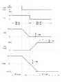
以下に、第1の実施形態の作用として、図4を参照しながら駆動回路10の動作を説明する。なお、図4では、特に時間軸を拡大して示している。また、図4では、駆動信号Cinに基づいて出力する制御電圧Vc、及びノード40の電圧VNに対応するソース電圧VSを括弧書きにより付記している。 The operation of the
駆動回路10に設けているコントロール回路36は、駆動信号CinがHレベルになることにより制御電圧Vcを電圧VCCに上昇させる。制御電圧Vcに応じてパワートランジスタPTrのゲート電圧VGが電圧VCCに上昇する。制御信号出力部46は、ゲート電圧VGが0v以上(例えば、VG=VCC)となることで制御信号CsをHレベルとする。駆動回路10は、制御信号CsがHレベルとなることで、トランジスタMaがオンし、トランジスタMbがオフする。トランジスタMaがオンすることによりパワートランジスタPTrのソースSが接地され、ゲートGの対ソース電圧VGSが電圧VCCとなってパワートランジスタPTrのオン状態が継続される。 The
一方、駆動回路10のコントロール回路36は、駆動信号CinがLレベルになることにより、パワートランジスタPTrのゲートGへ出力する制御電圧Vcを0vとする。図4に示すように、制御電圧Vcが0vとなることで、パワートランジスタPTrのゲート電圧VGが0vとなるように下降する。コントロール回路36は、ゲート電圧検出部44により検出するゲート電圧VGが0vまで低下する(VG=0v)と、制御信号出力部46が制御信号CsをLレベルにする。 On the other hand, the
駆動回路10は、制御信号CsがLレベルになることで、トランジスタMaがオフし、トランジスタMbがオンする。駆動回路10は、トランジスタMbがオンすることによりトランジスタMbを介して、電源ライン20からパワートランジスタPTrのソースSに電流が流れる。電源ライン20からソースSに電流が流れることでパワートランジスタPTrのソース電圧VSが上昇し、更に、パワートランジスタPTrのソース電圧VSが電圧VCCにクランプされる。 In the
パワートランジスタPTrのゲート電圧VGが低下し0v(VG=0v)となっている状態でソース電圧VSが上昇することで、パワートランジスタPTrのゲートGの対ソース電圧VGSが負となる。また、パワートランジスタPTrは、対ソース電圧VGSがしきい値電圧−Vthより下がる(VGS≦−Vth<0)ことでオフする。すなわち、ノーマリーオン形のパワートランジスタPTrは、ゲート電圧VGが0vの状態でソース電圧VSがしきい値電圧−Vthの絶対値Vthを超えることでオフする。 When the source voltage VS increases while the gate voltage VG of the power transistor PTr is reduced to 0 v (VG = 0 v), the source voltage VGS of the gate G of the power transistor PTr becomes negative. The power transistor PTr is turned off when the source-to-source voltage VGS falls below the threshold voltage −Vth (VGS ≦ −Vth <0). That is, the normally-on type power transistor PTr is turned off when the gate voltage VG is 0 v and the source voltage VS exceeds the absolute value Vth of the threshold voltage −Vth.
駆動回路10は、パワートランジスタPTrのゲート電圧VG及びソース電圧VSを逆相で制御することにより、ゲートGの対ソース電圧VGSをVCCから−VCCの範囲で制御する(−VCC≦VGS≦VCC)。パワートランジスタPTrは、ゲートGの対ソース電圧VGSが電圧VCCから電圧−VCCの範囲で制御されることで的確にオン・オフ駆動する。 The
電圧VCCは、しきい値電圧−Vthの絶対値Vthに対して十分高い電圧となっている。駆動回路10は、パワートランジスタPTrのゲート電圧VGを下げて、ソース電圧VSを高くすることで、対ソース電圧VGSをしきい値電圧Vthより低くする。従って、駆動回路10は、負電圧の電源を用いることなく、ノーマリーオン形のパワートランジスタPTrを的確にオフすることができる。 The voltage VCC is sufficiently higher than the absolute value Vth of the threshold voltage −Vth. The
更に、駆動回路10は、パワートランジスタPTrをオフする際に、トランジスタMbをオンし、パワートランジスタPTrのソースSに電圧VCCを供給することで、ソース電圧VSを上昇させる。従って、駆動回路10は、パワートランジスタPTrを迅速にオフすることができる。 Further, when turning off the power transistor PTr, the
一方、図1に示すように、パワートランジスタPTrのリード34及びワイヤボンディングに用いる配線には、少なからず寄生インダクタンスLpが存在する。図4に示すように、パワートランジスタPTrを例えば数psec〜数nsecの立下り信号高速駆動すると、寄生インダクタンスLpは、駆動回路10の出力端子28Cに過電圧(図4において二点鎖線で示す)を生じさせる。なお、以下では、過電圧をスパイク電圧Svとする。また、図4では、駆動回路10の出力端子28Cの電圧を、ノード40の電圧VNとして示している。 On the other hand, as shown in FIG. 1, the
スパイク電圧Svは、特に、パワートランジスタPTrが接続される電源ライン30の電圧VINが高電圧(例えば、百数十v〜数百v)であると、寄生インダクタンスLpに流れる電流が増大し、より大きな電圧となる。 The spike voltage Sv increases the current flowing through the parasitic inductance Lp particularly when the voltage VIN of the
トランジスタMaをオフしたとき、パワートランジスタPTrがオンしていることにより生じるスパイク電圧Svは、トランジスタMaのドレインDが接続されるノード40に印加される。トランジスタMaは、ノード40の電圧VNがスパイク電圧SvによりトランジスタMaの耐電圧を超えると破損等が生じる。 When the transistor Ma is turned off, the spike voltage Sv generated by turning on the power transistor PTr is applied to the
駆動回路10は、トランジスタMaのドレインDが接続されるノード40と電源ライン20との間にトランジスタMbを設け、トランジスタMaをオフする際にトランジスタMbをオンする。駆動回路10は、トランジスタMbがオンすることにより、電源ライン20とトランジスタMaのドレインD(ノード40)との間を導通状態とする。駆動回路10は、スパイク電圧Svによりノード40の電圧VNが電圧VCCを超える(VCC≦Sv)と、スパイク電圧Svに応じた電流Io(図1参照)がノード40からトランジスタMbを経て電源ライン20に流れる。従って、駆動回路10は、スパイク電圧Svが発生しても、ノード40に接続されているトランジスタMaのドレインDを電圧VCCにクランプする。 The
また、電源ライン20には、直流電源部16のコンデンサ22が接続されているので、スパイク電圧Svが発生しても、電圧VCCの上昇が抑えられる。従って、駆動回路10は、電圧VCCに基づいて設定した耐電圧のトランジスタMaを用いることができる。 Further, since the
駆動回路10は、スパイク電圧Svによる電力(エネルギー)を、電源ライン20に回生する。スパイク電圧Svによる電力は、電源ライン20に回生されることで、周辺回路18等により消費される。従って、駆動回路10は、寄生インダクタンスLp等に基因して生じるスパイク電圧Svに応じた電力を無駄に消費することなく、有効に利用することができる。 The
更に、駆動回路10は、スパイク電圧Svの抑制に、ショットキーバリアダイオード(Schottky barrier diode:SBD)やツェナーダイオード(Zenner diode)ではなく、トランジスタMbを用いる。従って、駆動回路10は、トランジスタMbを用いることで、特別なプロセスを用いることなく集積回路12に形成することができる。 Furthermore, the
また、駆動回路は、N型MOSFETのトランジスタMaに対して、P型MOSFETのトランジスタMbを用いている。従って、駆動回路10は、一つの制御信号CsをトランジスタMaのゲートG、及びトランジスタMbのゲートGに入力することで、トランジスタMaのオフ及びトランジスタMbのオフを的確に行うことができる。 The drive circuit uses a P-type MOSFET transistor Mb for an N-type MOSFET transistor Ma. Therefore, the
〔第2の実施形態〕
次に、開示の技術における第2の実施形態を説明する。第2の実施形態の基本的構成は、第1の実施形態と同様であり、第2の実施形態において第1の実施形態と同様の機能部品については、第1の実施形態と同様の符号を付与してその説明を省略する。[Second Embodiment]
Next, a second embodiment of the disclosed technology will be described. The basic configuration of the second embodiment is the same as that of the first embodiment. In the second embodiment, the same reference numerals as those of the first embodiment are used for the functional components similar to those of the first embodiment. The explanation is omitted.
図5には、第2の実施形態に係る駆動回路50を示している。駆動回路50は、各機能部品が第1の実施形態の駆動回路10と同じであるが、パワートランジスタPTsが接続される点で相違する。パワートランジスタPTsは、第1の実施形態のパワートランジスタPTrに替えて用いる。パワートランジスタPTsは、第2の実施形態において第1のスイッチング素子の一例として機能する。 FIG. 5 shows a
パワートランジスタPTsは、ノーマリーオフ形のトランジスタが適用されている。ノーマリーオフ形のパワートランジスタPTsは、しきい値電圧Vthが正の電圧(0v<Vth<VCC)となっている。従って、パワートランジスタPTsは、ゲート電圧Gが0vの状態でオフしている。 As the power transistor PTs, a normally-off type transistor is applied. The normally-off power transistor PTs has a positive threshold voltage Vth (0v <Vth <VCC). Therefore, the power transistor PTs is turned off when the gate voltage G is 0 v.
ノーマリーオフ形のパワートランジスタPTsを駆動する駆動回路50の動作を説明する。なお、以下に示す図6では、駆動信号Cinに基づいて出力する制御電圧Vc、及びノード40の電圧VNに対応するソース電圧VSを括弧書きにより付記している。 The operation of the
駆動回路50は、駆動信号CinがHレベルになることによりコントロール回路36から出力する制御電圧Vcが電圧VCCに上昇し、パワートランジスタPTsのゲート電圧VGを電圧VCCに上昇させる。制御信号出力部46は、ゲート電圧VGが0v以上(例えば、VG=VCC)となることで制御信号CsをHレベルにし、トランジスタMbをオフさせ、トランジスタMaをオンさせる。パワートランジスタPTsは、ゲートGの対ソース電圧VGSが、しきい値電圧Vthを超えることでオンする。 The
一方、駆動回路50は、駆動信号CinがLレベルになることにより、コントロール回路36からパワートランジスタPTsのゲートGへ出力する制御電圧Vcを0vとする。図6に示すように、制御電圧Vcが0vとなることで、パワートランジスタPTsのゲート電圧VGが0vとなるように下降する。コントロール回路36は、ゲート電圧検出部44により検出するゲート電圧VGが0vまで低下する(VG≦0v)と、制御信号出力部46が制御信号CsをLレベルとする。 On the other hand, the
ここで、ソース電圧VSが0vであると、パワートランジスタPTsのしきい値電圧Vthが正(0v<Vth<VCC)となっていることで、パワートランジスタPTsは、ゲート電圧VGが0vに達する前にオフする。駆動回路50は、ゲート電圧VGが0vとなると、トランジスタMaがオフし、トランジスタMbがオンする。 Here, if the source voltage VS is 0v, the threshold voltage Vth of the power transistor PTs is positive (0v <Vth <VCC), so that the power transistor PTs is before the gate voltage VG reaches 0v. Turn off. In the
ここで、パワートランジスタPTsがオフし、トランジスタMaがオフすることでスパイク電圧Sv(図6において二点鎖線で示す)が発生することがある。駆動回路50は、ノード40(トランジスタMaのドレインD)の電圧VNが電圧VCCを超えると、トランジスタMbを介して、電源ライン20に電流Ioが流れる。駆動回路50は、電流Ioが流れることにより、トランジスタMaのドレインDの電圧(電圧VN)が電圧VCCより高くなるのが抑えられる。 Here, when the power transistor PTs is turned off and the transistor Ma is turned off, a spike voltage Sv (indicated by a two-dot chain line in FIG. 6) may be generated. In the
従って、駆動回路50は、ノーマリーオフ形のパワートランジスタPTsをオン・オフ駆動する場合でも、スパイク電圧SvからトランジスタMa等を保護し、更に、スパイク電圧Svの電力を電源ライン20に回生する。 Therefore, the
以上説明した第1及び第2の実施形態では、単一の制御信号CsによりトランジスタMa及びトランジスタMbをオン・オフしたが、トランジスタMaとトランジスタMbのオン・オフは、異なるタイミングであっても良い。 In the first and second embodiments described above, the transistors Ma and Mb are turned on / off by a single control signal Cs. However, the transistors Ma and Mb may be turned on / off at different timings. .
〔第3の実施形態〕
次に開示の技術に係る第3の実施形態を説明する。なお、第3の実施形態の基本的構成は、第1の実施形態と同様であり、第3の実施形態において第1の実施形態と同様の機能部品については、第1の実施形態と同様の符号を付与してその説明を省略する。[Third Embodiment]
Next, a third embodiment according to the disclosed technique will be described. The basic configuration of the third embodiment is the same as that of the first embodiment. In the third embodiment, the same functional components as those of the first embodiment are the same as those of the first embodiment. Reference numerals are assigned and description thereof is omitted.
図7には、第3の実施形態に係る駆動回路60を示す。駆動回路60は、集積回路62に形成される。駆動回路60は、第3の実施形態において駆動回路の一例として機能し、集積回路62は、第3の実施形態において半導体集積回路の一例として機能する。 FIG. 7 shows a
駆動回路60は、コントロール回路64を備える。コントロール回路64は、第1の実施形態のコントロール回路36に替えて用いる。コントロール回路64は、入力端子38C、出力端子38D、38Eに加え、入力端子38F及び出力端子38Gを備える。コントロール回路64は、入力端子38Fが、駆動回路60のノード40(ノード40と出力端子26Cとの間)に接続されている。コントロール回路64は、入力端子38Fにノード40の電圧VNが入力される。駆動回路60では、通常、ノード40の電圧VNがパワートランジスタPTrのソース電圧VSとなっている。 The
コントロール回路64は、出力端子38Eが、トランジスタMaのゲートGに接続され、出力端子38GがトランジスタMbのゲートGに接続されている。コントロール回路64は、パワートランジスタPTrのゲート電圧VGに基づいて、トランジスタMaをオン・オフ制御する制御信号Csaを出力端子38EからトランジスタMaへ出力する。また、コントロール回路64は、パワートランジスタPTrのソース電圧VSとなるノード40の電圧VNに基づいて、トランジスタMbをオン・オフ制御する制御信号Csbを出力端子38GからトランジスタMbへ出力する。 The
図8には、コントロール回路64の一例を示す。コントロール回路64は、ソース電圧検出部66及び制御信号出力部68を含む。ソース電圧検出部66は、入力端子38Fに接続されており、入力端子38Fから入力されるパワートランジスタPTrのソース電圧VSを検出する。制御信号出力部68は、パワートランジスタPTrのソース電圧VSに応じて制御信号Csbを出力端子38GからトランジスタMbのゲートGへ出力する。 FIG. 8 shows an example of the
駆動回路60では、トランジスタMa、Mbがオフすることで、パワートランジスタPTrのソース電圧VSが上昇する。コントロール回路64の制御信号出力部68は、例えば、パワートランジスタPTrのソース電圧VSが電圧VCCに達するまでに、トランジスタMbをオンさせる制御信号Csbを出力する。 In the
駆動回路60は、駆動信号CinがHレベルになることによりコントロール回路64から出力する制御電圧Vcを電圧VCCに上昇させる。また、駆動回路60は、トランジスタMbをオフし、かつトランジスタMaをオンすることでパワートランジスタPTrのソース電圧VSを下げる。 The
パワートランジスタPTrは、ゲート電圧VGの上昇及びソース電圧VSの下降により、ゲートGの対ソース電圧VGSが上昇することでオンする。 The power transistor PTr is turned on when the gate-to-source voltage VGS of the gate G rises due to the rise of the gate voltage VG and the fall of the source voltage VS.
一方、駆動回路60は、駆動信号CinがLレベルになることにより、コントロール回路36からパワートランジスタPTrのゲートGへ出力する制御信号Vcを0vとする。図9に示すように、制御電圧Vcが0vとなることで、パワートランジスタPTrのゲート電圧VGが0vとなるように下降する。コントロール回路36は、ゲート電圧検出部44により検出するゲート電圧VGが0vまで低下する(VG≦0v)と、制御信号出力部46が制御信号CsaをLレベルにする。なお、図9では、駆動信号Cinに基づいて出力する制御電圧Vc、及びノード40の電圧VNに対応するソース電圧VSを括弧書きにより付記している。 On the other hand, the
ここで、パワートランジスタPTrのしきい値電圧Vthが負(−Vth、−VCC<−Vth<0v)となっていることで、パワートランジスタPTrは、ゲートGの対ソース電圧VGSが、しきい値電圧−Vthより下がるとオフする。 Here, since the threshold voltage Vth of the power transistor PTr is negative (−Vth, −VCC <−Vth <0 v), the power transistor PTr has a threshold voltage VGS of the gate G that is equal to the threshold voltage. It turns off when the voltage falls below -Vth.
また、駆動回路60のコントロール回路64は、パワートランジスタPTrのソース電圧VSが、電圧VCCに達するまでにトランジスタMbがオンするように制御信号CsbをトランジスタMbのゲートGへ出力する。 The
ここで、パワートランジスタPTrがオフし、トランジスタMaがオフすることでスパイク電圧Svが発生することがある。駆動回路60は、ソース電圧VSに応じたノード40の電圧VNが電圧VCCに達すると、トランジスタMbがオンされる。駆動回路60は、トランジスタMbがオンすることで、電源ライン20とノード40との間が導通状態となる。 Here, when the power transistor PTr is turned off and the transistor Ma is turned off, the spike voltage Sv may be generated. In the
駆動回路60は、ノード40の電圧VNが電圧VCCを超えると、トランジスタMbを介して、電源ライン20に電流Ioが流れる。駆動回路60は、電流Ioが流れることにより、トランジスタMaのドレインDの電圧(電圧VN)が電圧VCCより高くなるのが抑えられる。 In the
駆動回路60は、トランジスタMaをオフした後、ノード40の電圧VNが電圧VCCに達するまでにオンすることで、スパイク電圧SvからトランジスタMa等を保護することができる。また、駆動回路60は、ノード40の電圧VNが電圧VCCに達するまでにトランジスタMbをオンしていることで、スパイク電圧Svの電力を電源ライン20に回生する。 The
なお、駆動回路60は、ノーマリーオフ形のパワートランジスタPTsに対する駆動にも適用することができる。 The
以上説明した第1から第3の実施形態では、ゲート電圧VGがLレベル(0v)となったタイミングでトランジスタMaをオフしたが、トランジスタMaをオフするタイミングは、これに限るものではない。例えば、トランジスタMaは、制御電圧Vcを0vとするのに同期してオンされても良い。ゲート電圧VGが降下してからゲート電圧VGが0vに達するまでの間でオンされても良い。 In the first to third embodiments described above, the transistor Ma is turned off at the timing when the gate voltage VG becomes the L level (0 v). However, the timing at which the transistor Ma is turned off is not limited thereto. For example, the transistor Ma may be turned on in synchronization with the control voltage Vc being 0 v. It may be turned on between the time when the gate voltage VG drops and the time when the gate voltage VG reaches 0v.
また、トランジスタMbは、トランジスタMaのオフに合わせてオンされ、トランジスタMaのオンに合わせてオフされることが好ましいがこれに限るものではない。トランジスタMbは、トランジスタMaがオンしているときにオンされなければ良く、かつ、トランジスタMaがオフしているときに、トランジスタMaのドレインDの電圧が電圧VCCに達するまでにオンされれば良い。 The transistor Mb is preferably turned on when the transistor Ma is turned off and turned off when the transistor Ma is turned on. However, the present invention is not limited to this. The transistor Mb may not be turned on when the transistor Ma is turned on, and may be turned on until the voltage at the drain D of the transistor Ma reaches the voltage VCC when the transistor Ma is turned off. .
また、トランジスタMa、Mbのオン・オフのタイミングは、駆動信号Cinに基づいて設定しても良い。駆動信号Cinに基づいてトランジスタMa、Mbをオン・オフする場合、制御電圧Vcに同期させてトランジスタMa、Mbをオン・オフしても良い。 The on / off timing of the transistors Ma and Mb may be set based on the drive signal Cin. When the transistors Ma and Mb are turned on / off based on the drive signal Cin, the transistors Ma and Mb may be turned on / off in synchronization with the control voltage Vc.
また、駆動信号Cinに基づいてトランジスタMa、Mbをオン・オフする場合、制御電圧Vcのオフに対して所定時間だけ遅延させてトランジスタMaのオフ及びトランジスタMbのオンを行っても良い。なお、制御電圧Vcをオンする際は、トランジスタMaのオン及びトランジスタMbのオフに対して遅延させて制御電圧Vcをオンする。 When the transistors Ma and Mb are turned on / off based on the drive signal Cin, the transistor Ma may be turned off and the transistor Mb may be turned on by delaying the control voltage Vc by a predetermined time. When the control voltage Vc is turned on, the control voltage Vc is turned on with a delay from the turning on of the transistor Ma and the turning off of the transistor Mb.
開示の技術においては、通電素子は、一方の電位が他方の電位より高くなった際に通電を許容する機能を備える素子、機能部品を適用することを含む。第1から第3の実施形態では、通電素子の一例としてトランジスタMbを用いたが、通電素子は、これに限るものではなく、例えば、シリコンダイオードを用いても良い。 In the disclosed technology, the energization element includes applying an element or a functional component having a function of allowing energization when one potential becomes higher than the other potential. In the first to third embodiments, the transistor Mb is used as an example of the energization element. However, the energization element is not limited thereto, and for example, a silicon diode may be used.
図10には、駆動回路70を示す。駆動回路70は、集積回路72に形成される。駆動回路70は、第1の実施形態の駆動回路10についてトランジスタMbに替えてシリコンダイオード(以下、ダイオード74とする)を用いる。 FIG. 10 shows the
ダイオード74は、カソードKが電源端子24Aに接続され、アノードAがノード40に接続されている。駆動回路70は、ノード40の電圧VNが電圧VCCにより低い状態ではダイオード74により電流の流れが阻止される。 The
また、駆動回路70は、ノード40の電圧VNが電圧VCCを超える場合において導通状態となり、ノード40から電源ライン20へ向けた電流Ioの流れが許容される。従って、ダイオード74を用いた駆動回路70は、スパイク電圧Svを抑制し、かつ、スパイク電圧Svの電力を電源ライン20へ回生する。 In addition,
開示の技術は、上記実施の形態に記載に限らず、各部分が目的とする機能を含む形態であれば良い。また、本明細書に記載された全ての特許出願及び特許出願に開示される技術文献は、個々の文献、特許出願及び技術規格が参照により取り込まれることが具体的かつ個々に記された場合と同程度に、本明細書中に、参照により取り込まれる。 The disclosed technology is not limited to the above-described embodiment, and any form may be used as long as each part includes a target function. In addition, all patent applications and technical documents disclosed in the patent application described in this specification include cases where individual documents, patent applications, and technical standards are specifically and individually described to be incorporated by reference. To the same extent, it is incorporated herein by reference.
開示の技術は以下の付記を含む。 The disclosed technology includes the following supplementary notes.
(付記1)
第1のスイッチング素子のソースに直列に接続され、前記第1のスイッチング素子がオンされるときにオンされ、前記第1のスイッチング素子がオフされるときにオフされる第2のスイッチング素子と、
前記第2のスイッチング素子のドレインと電源ラインとの間に設けられ、前記第2のスイッチング素子をオフさせる信号に応じて、前記第2のスイッチング素子のドレインを前記電源ラインに接続する通電素子と、
を含む駆動回路。(Appendix 1)
A second switching element connected in series to a source of the first switching element, turned on when the first switching element is turned on, and turned off when the first switching element is turned off;
An energization element provided between the drain of the second switching element and the power supply line, and connecting the drain of the second switching element to the power supply line in response to a signal for turning off the second switching element; ,
Including a driving circuit.
(付記2)
前記通電素子は第3のスイッチング素子を有し、
前記第1のスイッチング素子の駆動信号に応じ、前記第1のスイッチング素子、前記第2のスイッチング素子、及び前記第3のスイッチング素子のオン・オフの制御を行う制御部を含む付記1記載の駆動回路。(Appendix 2)
The energization element has a third switching element;
The drive according to
(付記3)
第1のスイッチング素子のソースに直列に接続された第2のスイッチング素子と、
前記第2のスイッチング素子のドレインと電源ラインとの間に接続された第3のスイッチング素子と、
前記第1のスイッチング素子の駆動信号に応じ、前記第1のスイッチング素子のゲートへ出力する電圧を制御し、前記第1のスイッチング素子をオンさせるときに、前記第2のスイッチング素子をオンさせ、かつ前記第3のスイッチング素子をオフさせ、前記第1のスイッチング素子をオフするときに、前記第2のスイッチング素子をオフさせ、かつ前記第3のスイッチング素子をオンさせる制御部と、
を含む駆動回路。(Appendix 3)
A second switching element connected in series to the source of the first switching element;
A third switching element connected between the drain of the second switching element and a power supply line;
In response to the drive signal of the first switching element, the voltage output to the gate of the first switching element is controlled, and when turning on the first switching element, the second switching element is turned on, And a controller that turns off the second switching element and turns on the third switching element when turning off the third switching element and turning off the first switching element;
Including a driving circuit.
(付記4)
前記制御部は、前記第2のスイッチング素子をオフさせる前記制御信号に応じて前記第3のスイッチング素子をオンさせる、付記2又は付記3記載の駆動回路。(Appendix 4)
The drive circuit according to appendix 2 or
(付記5)
前記制御部は、前記第2のスイッチング素子をオフさせた後、前記第3のスイッチング素子をオンさせる、付記2又は付記3記載の駆動回路。(Appendix 5)
The drive circuit according to appendix 2 or
(付記6)
前記制御部は、前記第1のスイッチング素子のゲート電圧が所定値に低下することで前記第2のスイッチング素子をオフさせ、前記第3のスイッチング素子をオンさせる、付記4又は付記5記載の駆動回路。(Appendix 6)
The drive according to
(付記7)
前記第1のスイッチング素子が、ノーマリーオン形のスイッチング素子である、付記1から付記6のいずれかに記載の駆動回路。(Appendix 7)
The drive circuit according to any one of
(付記8)
第1のスイッチング素子のソースに直列に接続され、前記第1のスイッチング素子がオンされるときにオンされ、前記第1のスイッチング素子がオフされるときにオフされる第2のスイッチング素子と、
前記第2のスイッチング素子のドレインと電源ラインとの間に設けられ、前記第2のスイッチング素子をオフさせる制御信号に応じて、前記第2のスイッチング素子のドレインを前記電源ラインに接続する通電素子と、
を備える駆動回路を含む半導体集積回路(Appendix 8)
A second switching element connected in series to a source of the first switching element, turned on when the first switching element is turned on, and turned off when the first switching element is turned off;
An energization element that is provided between the drain of the second switching element and the power supply line and connects the drain of the second switching element to the power supply line in response to a control signal for turning off the second switching element. When,
Integrated circuit including a drive circuit comprising
(付記9)
前記通電素子は第3のスイッチング素子を有し、
前記第1のスイッチング素子の駆動信号に応じ、第1のスイッチング素子、前記第2のスイッチング素子、及び前記第3のスイッチング素子のオン・オフの制御を行う制御部と、
を含む付記8記載の半導体集積回路。(Appendix 9)
The energization element has a third switching element;
A controller that controls on / off of the first switching element, the second switching element, and the third switching element in accordance with a drive signal of the first switching element;
The semiconductor integrated circuit according to appendix 8, including:
(付記10)
第1のスイッチング素子のソースに直列に接続された第2のスイッチング素子と、
前記第2のスイッチング素子のドレインと電源ラインとの間に接続された第3のスイッチング素子と、
前記第1のスイッチング素子の駆動信号に応じ、第1のスイッチング素子のゲートへ出力する電圧を制御し、前記第1のスイッチング素子をオンさせるときに、前記第2のスイッチング素子をオンさせ、かつ前記第3のスイッチング素子をオフさせ、前記第1のスイッチング素子をオフするときに、前記第2のスイッチング素子をオフさせ、かつ前記第3のスイッチング素子をオンさせる制御部と、
を備える駆動回路を含む半導体集積回路。(Appendix 10)
A second switching element connected in series to the source of the first switching element;
A third switching element connected between the drain of the second switching element and a power supply line;
Controlling the voltage output to the gate of the first switching element according to the drive signal of the first switching element, turning on the second switching element when turning on the first switching element; and A control unit for turning off the third switching element, turning off the second switching element and turning on the third switching element when turning off the first switching element;
A semiconductor integrated circuit including a drive circuit comprising:
(付記11)
前記制御部は、前記第2のスイッチング素子をオフさせる前記制御信号に応じて前記第3のスイッチング素子をオンさせる、付記9又は付記10記載の半導体集積回路。(Appendix 11)
The semiconductor integrated circuit according to appendix 9 or
(付記12)
前記制御部は、前記第2のスイッチング素子をオフさせた後、前記第3のスイッチング素子をオンさせる、付記9又は付記10記載の半導体集積回路。(Appendix 12)
The semiconductor integrated circuit according to appendix 9 or
(付記13)
前記制御部は、前記第1のスイッチング素子のゲート電圧が所定値に低下することで前記第2のスイッチング素子をオフさせ、前記第3のスイッチング素子をオンさせる、付記11又は付記12記載の半導体集積回路。(Appendix 13)
The semiconductor according to appendix 11 or
(付記14)
前記第1のスイッチング素子が、ノーマリーオン形のスイッチング素子である、付記8から付記13のいずれかに記載の半導体集積回路。(Appendix 14)
14. The semiconductor integrated circuit according to any one of appendix 8 to appendix 13, wherein the first switching element is a normally-on type switching element.
(付記15)
第1のスイッチング素子をオンする際に、前記第1のスイッチング素子のソースに直列に接続された第2のスイッチング素子をオンし、
前記第1のスイッチング素子をオフする際に、前記第2のスイッチング素子をオフし、 前記第2のスイッチング素子のドレインと電源ラインとの間に設けた通電素子により前記第2のスイッチング素子のドレインを前記電源ラインに接続する、
ことを含む駆動回路の制御方法。(Appendix 15)
When turning on the first switching element, turning on the second switching element connected in series to the source of the first switching element;
When turning off the first switching element, the second switching element is turned off, and the drain of the second switching element is provided by a current-carrying element provided between the drain of the second switching element and a power supply line. Connect to the power line,
A method for controlling the driving circuit.
(付記16)
前記通電素子は第3のスイッチング素子を有し、前記第3のスイッチング素子をオンすることで、前記第2のスイッチング素子のドレインを前記電源ラインに接続する、
ことを含む付記15記載の駆動回路の制御方法。(Appendix 16)
The energization element includes a third switching element, and the drain of the second switching element is connected to the power line by turning on the third switching element.
The control method of the drive circuit of Additional remark 15 including this.
10、50、60、70 駆動回路
12、52、62、72 集積回路
14 基板
16 直流電源部
18 周辺回路
20 電源ライン
22 コンデンサ
28 負荷
30 電源ライン
32 パッケージ
34 リード
36、74 コントロール回路
40 ノード
42 ゲート電圧制御部
44 ゲート電圧検出部
46、68 制御信号出力部
66 ソース電圧検出部
74 ダイオード
PTr パワートランジスタ
PTs パワートランジスタ
Ma トランジスタ
Mb トランジスタ
10, 50, 60, 70
Claims (5)
Translated fromJapanese前記第2のスイッチング素子のドレインと電源ラインとの間に設けられ、前記第2のスイッチング素子をオフさせる信号に応じて、前記第2のスイッチング素子のドレインを前記電源ラインに接続する第3のスイッチング素子と、
前記第1のスイッチング素子の駆動信号に応じ、前記第1のスイッチング素子、前記第2のスイッチング素子、及び前記第3のスイッチング素子のオン・オフの制御を行う制御部と、
を含む駆動回路。A second switching element connected in series to a source of the first switching element, turned on when the first switching element is turned on, and turned off when the first switching element is turned off;
A third switch is provided between the drain of the second switching element and the power supply line and connects the drain of the second switching element to the power supply line in response to a signal for turning off the second switching element. A switching element;
A controller that controls on / off of the first switching element, the second switching element, and the third switching element in response to a drive signal of the first switching element;
Including a driving circuit.
前記第2のスイッチング素子のドレインと電源ラインとの間に設けられ、前記第2のスイッチング素子をオフさせる制御信号に応じて、前記第2のスイッチング素子のドレインを前記電源ラインに接続する第3のスイッチング素子と、
前記第1のスイッチング素子の駆動信号に応じ、第1のスイッチング素子、前記第2のスイッチング素子、及び前記第3のスイッチング素子のオン・オフ制御を行う制御部と、
を備えた駆動回路を含む半導体集積回路。A second switching element connected in series to a source of the first switching element, turned on when the first switching element is turned on, and turned off when the first switching element is turned off;
The third switching element is provided between the drain of the second switching element and the power supply line, and connects the drain of the second switching element to the power supply line in response to a control signal for turning off the second switching element. Switching elements of
A controller that performs on / off control of the first switching element, the second switching element, and the third switching element according to a drive signal of the first switching element;
A semiconductor integrated circuit including a driving circuitwith.
前記制御部が、前記第1のスイッチング素子をオフする際に、前記第2のスイッチング素子をオフし、前記第3のスイッチング素子をオンすることにより前記第2のスイッチング素子のドレインを前記電源ラインに接続し、
前記制御部は、前記第1のスイッチング素子の駆動信号に応じ、前記第1のスイッチング素子、前記第2のスイッチング素子、及び前記第3のスイッチング素子のオン・オフの制御を行う、
ことを含む駆動回路の制御方法。When the control unit turns on the first switching element, thecontrol unit turns on the second switching element connected in series to the source of the firstswitching element, and the drain of the second switching element, the power supply line, And turn off the third switching element provided between
When the control unit turns off the first switching element, thecontrol unit turns off the second switching element and turns onthe third switching element, thereby connecting the drain of the second switching element to the power supply line. Connectedto
The control unit performs on / off control of the first switching element, the second switching element, and the third switching element according to a drive signal of the first switching element.
A method for controlling the driving circuit.
Priority Applications (3)
| Application Number | Priority Date | Filing Date | Title |
|---|---|---|---|
| JP2013080261AJP6065721B2 (en) | 2013-04-08 | 2013-04-08 | Drive circuit, semiconductor integrated circuit, and drive circuit control method |
| US14/229,332US9059697B2 (en) | 2013-04-08 | 2014-03-28 | Drive circuit and drive method for driving normally-on-type transistor |
| CN201410126132.9ACN104104369B (en) | 2013-04-08 | 2014-03-31 | The control method of drive circuit, semiconductor integrated circuit and drive circuit |
Applications Claiming Priority (1)
| Application Number | Priority Date | Filing Date | Title |
|---|---|---|---|
| JP2013080261AJP6065721B2 (en) | 2013-04-08 | 2013-04-08 | Drive circuit, semiconductor integrated circuit, and drive circuit control method |
Publications (2)
| Publication Number | Publication Date |
|---|---|
| JP2014204354A JP2014204354A (en) | 2014-10-27 |
| JP6065721B2true JP6065721B2 (en) | 2017-01-25 |
Family
ID=51654014
Family Applications (1)
| Application Number | Title | Priority Date | Filing Date |
|---|---|---|---|
| JP2013080261AExpired - Fee RelatedJP6065721B2 (en) | 2013-04-08 | 2013-04-08 | Drive circuit, semiconductor integrated circuit, and drive circuit control method |
Country Status (3)
| Country | Link |
|---|---|
| US (1) | US9059697B2 (en) |
| JP (1) | JP6065721B2 (en) |
| CN (1) | CN104104369B (en) |
Families Citing this family (8)
| Publication number | Priority date | Publication date | Assignee | Title |
|---|---|---|---|---|
| JP2016139996A (en)* | 2015-01-28 | 2016-08-04 | 株式会社東芝 | Semiconductor device |
| JP2016139997A (en)* | 2015-01-28 | 2016-08-04 | 株式会社東芝 | Semiconductor device |
| CN107852157B (en)* | 2015-05-27 | 2021-11-02 | 威电科技有限公司 | Switching power supply device |
| US9813009B1 (en)* | 2017-02-07 | 2017-11-07 | Ford Global Technologies, Llc | Active gate clamping for inverter switching devices using grounded gate terminals |
| TWI705664B (en)* | 2020-01-08 | 2020-09-21 | 大陸商上海瀚薪科技有限公司 | Silicon carbide power element, drive circuit and control method |
| CN113162377B (en)* | 2020-01-22 | 2025-03-21 | 上海瀚薪科技有限公司 | A silicon carbide power component, drive circuit and control method |
| JP7610402B2 (en)* | 2020-12-22 | 2025-01-08 | 日立Astemo株式会社 | Load Driver |
| US20240283351A1 (en)* | 2023-02-17 | 2024-08-22 | Power Integrations, Inc. | Detecting signals from cascode power devices |
Family Cites Families (10)
| Publication number | Priority date | Publication date | Assignee | Title |
|---|---|---|---|---|
| JPH10276076A (en) | 1997-03-31 | 1998-10-13 | Oki Electric Ind Co Ltd | Semiconductor circuit |
| US6097220A (en)* | 1997-06-11 | 2000-08-01 | Intel Corporation | Method and circuit for recycling charge |
| CN1856929A (en)* | 2003-09-25 | 2006-11-01 | 皇家飞利浦电子股份有限公司 | A switch mode power converter |
| US7928702B2 (en)* | 2005-04-13 | 2011-04-19 | International Rectifier Corporation | Driving circuit for use with high voltage depletion-mode semiconductor switches |
| JP4844007B2 (en) | 2005-05-18 | 2011-12-21 | 富士電機株式会社 | Composite type semiconductor device |
| US8330492B2 (en)* | 2006-06-02 | 2012-12-11 | Semiconductor Energy Laboratory Co., Ltd. | Liquid crystal display device and electronic device |
| US7567097B2 (en)* | 2007-09-29 | 2009-07-28 | Hewlett-Packard Development Company, L.P. | Pre-driver circuit and appparatus using same |
| JP5565336B2 (en)* | 2011-02-14 | 2014-08-06 | 富士通セミコンダクター株式会社 | Output circuit, system, and output circuit control method |
| JP5910395B2 (en)* | 2011-09-16 | 2016-04-27 | サンケン電気株式会社 | Drive circuit |
| CN104205638B (en)* | 2012-03-27 | 2017-07-04 | 夏普株式会社 | cascode circuit |
- 2013
- 2013-04-08JPJP2013080261Apatent/JP6065721B2/ennot_activeExpired - Fee Related
- 2014
- 2014-03-28USUS14/229,332patent/US9059697B2/ennot_activeExpired - Fee Related
- 2014-03-31CNCN201410126132.9Apatent/CN104104369B/ennot_activeExpired - Fee Related
Also Published As
| Publication number | Publication date |
|---|---|
| CN104104369A (en) | 2014-10-15 |
| US9059697B2 (en) | 2015-06-16 |
| US20140300394A1 (en) | 2014-10-09 |
| JP2014204354A (en) | 2014-10-27 |
| CN104104369B (en) | 2017-09-01 |
Similar Documents
| Publication | Publication Date | Title |
|---|---|---|
| JP6065721B2 (en) | Drive circuit, semiconductor integrated circuit, and drive circuit control method | |
| KR102812897B1 (en) | INTEGRATED FAILSAFE PULLDOWN CIRCUIT FOR GaN SWITCH | |
| JP6402591B2 (en) | Semiconductor device | |
| US9935551B2 (en) | Switching circuit including serially connected transistors for reducing transient current at time of turning off, and power supply circuit provided therewith | |
| US8648643B2 (en) | Semiconductor power modules and devices | |
| US9362903B2 (en) | Gate drivers for circuits based on semiconductor devices | |
| JP5290354B2 (en) | Semiconductor device and electronic equipment | |
| JP2020018164A (en) | Method for operating circuit and circuit | |
| JP6264491B1 (en) | Short-circuit detection device and device | |
| JP5263317B2 (en) | Semiconductor switching element drive circuit | |
| WO2013077105A1 (en) | Inverter device | |
| CN111758210B (en) | Rectifying circuit and power supply device | |
| JP5619673B2 (en) | Switching circuit and semiconductor module | |
| KR102112299B1 (en) | Driving method and driving circuit for power switching device | |
| CN109936351B (en) | Semiconductor device and power module | |
| JP6988256B2 (en) | Power converter | |
| CN112534668B (en) | Boost converter short circuit protection | |
| KR102284188B1 (en) | GATE DRIVING CIRCUIT FOR SiC MOSFET | |
| US20170179825A1 (en) | Switched mode power supply converter | |
| JP5843535B2 (en) | Semiconductor module | |
| JP6950443B2 (en) | Semiconductor switching element drive circuit and power converter | |
| WO2016030998A1 (en) | Power conversion device, motor device, and inverter module | |
| JP5862232B2 (en) | Overvoltage protection circuit | |
| CN110741546A (en) | Rectifier circuit and power supply device | |
| JP6265849B2 (en) | Control circuit |
Legal Events
| Date | Code | Title | Description |
|---|---|---|---|
| A711 | Notification of change in applicant | Free format text:JAPANESE INTERMEDIATE CODE: A712 Effective date:20150608 | |
| A621 | Written request for application examination | Free format text:JAPANESE INTERMEDIATE CODE: A621 Effective date:20160105 | |
| A977 | Report on retrieval | Free format text:JAPANESE INTERMEDIATE CODE: A971007 Effective date:20160804 | |
| A131 | Notification of reasons for refusal | Free format text:JAPANESE INTERMEDIATE CODE: A131 Effective date:20160809 | |
| A521 | Request for written amendment filed | Free format text:JAPANESE INTERMEDIATE CODE: A523 Effective date:20161005 | |
| TRDD | Decision of grant or rejection written | ||
| A01 | Written decision to grant a patent or to grant a registration (utility model) | Free format text:JAPANESE INTERMEDIATE CODE: A01 Effective date:20161129 | |
| A61 | First payment of annual fees (during grant procedure) | Free format text:JAPANESE INTERMEDIATE CODE: A61 Effective date:20161212 | |
| R150 | Certificate of patent or registration of utility model | Ref document number:6065721 Country of ref document:JP Free format text:JAPANESE INTERMEDIATE CODE: R150 | |
| LAPS | Cancellation because of no payment of annual fees |