JP6058533B2 - Transparent light emitting device with controlled emission - Google Patents
Transparent light emitting device with controlled emissionDownload PDFInfo
- Publication number
- JP6058533B2 JP6058533B2JP2013514821AJP2013514821AJP6058533B2JP 6058533 B2JP6058533 B2JP 6058533B2JP 2013514821 AJP2013514821 AJP 2013514821AJP 2013514821 AJP2013514821 AJP 2013514821AJP 6058533 B2JP6058533 B2JP 6058533B2
- Authority
- JP
- Japan
- Prior art keywords
- region
- light emitting
- layer
- transparent
- emitting device
- Prior art date
- Legal status (The legal status is an assumption and is not a legal conclusion. Google has not performed a legal analysis and makes no representation as to the accuracy of the status listed.)
- Expired - Fee Related
Links
Images


Classifications
- H—ELECTRICITY
- H10—SEMICONDUCTOR DEVICES; ELECTRIC SOLID-STATE DEVICES NOT OTHERWISE PROVIDED FOR
- H10K—ORGANIC ELECTRIC SOLID-STATE DEVICES
- H10K71/00—Manufacture or treatment specially adapted for the organic devices covered by this subclass
- H10K71/60—Forming conductive regions or layers, e.g. electrodes
- H—ELECTRICITY
- H10—SEMICONDUCTOR DEVICES; ELECTRIC SOLID-STATE DEVICES NOT OTHERWISE PROVIDED FOR
- H10H—INORGANIC LIGHT-EMITTING SEMICONDUCTOR DEVICES HAVING POTENTIAL BARRIERS
- H10H20/00—Individual inorganic light-emitting semiconductor devices having potential barriers, e.g. light-emitting diodes [LED]
- H10H20/80—Constructional details
- H10H20/83—Electrodes
- H10H20/832—Electrodes characterised by their material
- H10H20/833—Transparent materials
- H—ELECTRICITY
- H10—SEMICONDUCTOR DEVICES; ELECTRIC SOLID-STATE DEVICES NOT OTHERWISE PROVIDED FOR
- H10K—ORGANIC ELECTRIC SOLID-STATE DEVICES
- H10K10/00—Organic devices specially adapted for rectifying, amplifying, oscillating or switching; Organic capacitors or resistors having potential barriers
- H10K10/80—Constructional details
- H10K10/82—Electrodes
- H—ELECTRICITY
- H10—SEMICONDUCTOR DEVICES; ELECTRIC SOLID-STATE DEVICES NOT OTHERWISE PROVIDED FOR
- H10K—ORGANIC ELECTRIC SOLID-STATE DEVICES
- H10K50/00—Organic light-emitting devices
- H10K50/80—Constructional details
- H10K50/805—Electrodes
- H10K50/81—Anodes
- H—ELECTRICITY
- H10—SEMICONDUCTOR DEVICES; ELECTRIC SOLID-STATE DEVICES NOT OTHERWISE PROVIDED FOR
- H10K—ORGANIC ELECTRIC SOLID-STATE DEVICES
- H10K50/00—Organic light-emitting devices
- H10K50/80—Constructional details
- H10K50/805—Electrodes
- H10K50/81—Anodes
- H10K50/814—Anodes combined with auxiliary electrodes, e.g. ITO layer combined with metal lines
- H—ELECTRICITY
- H10—SEMICONDUCTOR DEVICES; ELECTRIC SOLID-STATE DEVICES NOT OTHERWISE PROVIDED FOR
- H10K—ORGANIC ELECTRIC SOLID-STATE DEVICES
- H10K2102/00—Constructional details relating to the organic devices covered by this subclass
- H10K2102/301—Details of OLEDs
- H10K2102/302—Details of OLEDs of OLED structures
- H10K2102/3023—Direction of light emission
- H10K2102/3031—Two-side emission, e.g. transparent OLEDs [TOLED]
- H—ELECTRICITY
- H10—SEMICONDUCTOR DEVICES; ELECTRIC SOLID-STATE DEVICES NOT OTHERWISE PROVIDED FOR
- H10K—ORGANIC ELECTRIC SOLID-STATE DEVICES
- H10K2102/00—Constructional details relating to the organic devices covered by this subclass
- H10K2102/301—Details of OLEDs
- H10K2102/311—Flexible OLED
- H—ELECTRICITY
- H10—SEMICONDUCTOR DEVICES; ELECTRIC SOLID-STATE DEVICES NOT OTHERWISE PROVIDED FOR
- H10K—ORGANIC ELECTRIC SOLID-STATE DEVICES
- H10K50/00—Organic light-emitting devices
- H10K50/80—Constructional details
- H10K50/805—Electrodes
- H10K50/81—Anodes
- H10K50/813—Anodes characterised by their shape
- H—ELECTRICITY
- H10—SEMICONDUCTOR DEVICES; ELECTRIC SOLID-STATE DEVICES NOT OTHERWISE PROVIDED FOR
- H10K—ORGANIC ELECTRIC SOLID-STATE DEVICES
- H10K59/00—Integrated devices, or assemblies of multiple devices, comprising at least one organic light-emitting element covered by group H10K50/00
- H10K59/10—OLED displays
- H10K59/221—Static displays, e.g. displaying permanent logos
- H—ELECTRICITY
- H10—SEMICONDUCTOR DEVICES; ELECTRIC SOLID-STATE DEVICES NOT OTHERWISE PROVIDED FOR
- H10K—ORGANIC ELECTRIC SOLID-STATE DEVICES
- H10K59/00—Integrated devices, or assemblies of multiple devices, comprising at least one organic light-emitting element covered by group H10K50/00
- H10K59/30—Devices specially adapted for multicolour light emission
- H10K59/32—Stacked devices having two or more layers, each emitting at different wavelengths
Landscapes
- Physics & Mathematics (AREA)
- Optics & Photonics (AREA)
- Engineering & Computer Science (AREA)
- Manufacturing & Machinery (AREA)
- Electroluminescent Light Sources (AREA)
Description
Translated fromJapanese本発明は、エミッション制御を有する透明発光デバイスに関する。 The present invention relates to a transparent light emitting device having emission control.
有機発光デバイスは、光を放射(エミッション)することができるように一方が少なくとも部分的に透明にされた2つの電極間に有機発光層を配置するという原理に基づく。高い透明度を有する電極を用いることにより、高エミッションひいては高効率を達成することができる。現在、双方の電極が少なくとも部分的に透明にされる透明有機発光デバイス(OLED)に、開発の焦点が当てられている。故に、透明OLEDデバイスは、正面及び背面の双方において同時に放射する。幾つかの用途では、両方向に放射を有することが望まれ得る。しかしながら、他の用途では、放射方向を制御することが好ましい。例えば、発光デバイスの背面からの抑制された放射又は放射なし、及び発光デバイスの正面からの良好な放射、と組み合わせて高い透明度を有することが有利となり得る。 Organic light-emitting devices are based on the principle of placing an organic light-emitting layer between two electrodes, one of which is at least partially transparent so that it can emit light. By using an electrode having high transparency, high emission and consequently high efficiency can be achieved. Currently, development is focused on transparent organic light emitting devices (OLEDs) in which both electrodes are at least partially transparent. Thus, transparent OLED devices emit simultaneously on both the front and back. In some applications it may be desirable to have radiation in both directions. However, in other applications it is preferable to control the radiation direction. For example, it may be advantageous to have a high transparency in combination with suppressed or no radiation from the back of the light emitting device and good radiation from the front of the light emitting device.
特許文献1に、アノードとカソードとの間の有機層と、アノード上あるいはカソード上のミラー層とを有し、ミラー層が不透明ゾーンと透明ゾーン内とに構造化されたOLEDが記載されている。このOLEDは透明ゾーン内で完全あるいは部分的に非活性化されることができる。この構造により、光に対してOLEDを透明にすることができると同時に、エミッションを或る程度まで制御することができる。不透明なミラーゾーンは光放出を阻止し、光を所望方向に反射する。 Patent Document 1 describes an OLED having an organic layer between an anode and a cathode and a mirror layer on the anode or the cathode, the mirror layer being structured in an opaque zone and a transparent zone. . The OLED can be completely or partially deactivated in the transparent zone. With this structure, the OLED can be made transparent to light, and at the same time, the emission can be controlled to some extent. The opaque mirror zone blocks light emission and reflects light in the desired direction.
しかしながら、依然として、透明発光デバイスのエミッション制御を向上させるソリューションが技術的に望まれる。 However, there remains a technical desire for a solution that improves the emission control of transparent light emitting devices.
本発明の1つの目的は、従来技術の問題を少なくとも部分的に解決し、改善されたエミッション制御を有する発光デバイスと、そのようなデバイスを製造する有利な方法とを提供することである。 One object of the present invention is to at least partially solve the problems of the prior art and to provide a light emitting device with improved emission control and an advantageous method of manufacturing such a device.
第1の態様によれば、本発明は発光デバイスに関し、当該発光デバイスは、透明基板と、前記基板上に配置された、部分的に透明なアノード層又はアノード層アセンブリと、前記アノード層上に配置された発光層と、前記発光層上に配置された透明カソード層とを有し、前記アノード層又はアノード層アセンブリは、前記基板に面する第1表面と、前記発光層に面し且つ前記第1表面と反対側に位置する第2表面とを有し、前記第1表面は透明導電材料を有し、前記第2表面は、第1領域及び第2領域を有する金属層を有し、該金属層は、前記第1領域内では非酸化形態にあり且つ前記第2領域内では酸化された少なくとも1つの金属又は合金を有し、前記第1領域は導電性且つ不透明であり、前記第2領域は透明且つ電気絶縁性であり、且つ前記第1領域は、前記発光層と直接的に接触し、前記第1表面と前記発光層との間の電気接触を可能にするように構成される。それにより、非常に効率的な放射方向の制御が達成される。例えば、本発明は、改善された片面放射型透明OLEDデバイスの製造と、デバイスの一方の面で1つの色の光を放射し且つ反対側の面で第2の色の光を放射する透明発光デバイスの製造とを可能にする。放射方向の高度な制御が達成され得るのと同時に、この発光デバイスは、高い光透明性を有するように製造されることができる。According to a first aspect, the present invention relates to a light emitting device, the light emitting device comprising a transparent substrate, a partially transparent anode layer or anode layer assembly disposed on the substrate, and on the anode layer. A light emitting layer disposed and a transparent cathode layer disposed on the light emitting layer, the anode layer or anode layer assembly facing the substrate, a first surface facing the substrate, and the light emitting layer A second surface located opposite to the first surface, the first surface comprises a transparent conductive material, the second surface comprises a metal layer having a first region and a second region, The metal layer has at least one metal or alloy in a non-oxidized form in the first region and oxidized in the second region, the first region being conductive and opaque, Two areas are transparent and electrically insulating, and Said first region, said direct contact with the emitting layer configured to allow electrical contact between the emitting layer and the first surface. Thereby, very efficient radial control is achieved. For example, the present invention provides for the manufacture of an improved single-sided transparent OLED device and transparent light emission that emits one color of light on one side of the device and a second color of light on the opposite side. Enables device manufacturing. At the same time advanced control of the radiation direction can be achieved, the light emitting device can be manufacturedto have high optical transparency.
本発明の実施形態において、発光デバイスのアノードの第1表面は導電性ポリマーを有する。導電性ポリマーを用いることにより、改善された柔軟性を有する発光デバイスを得ることができる。 In an embodiment of the present invention, the first surface of the anode of the light emitting device has a conductive polymer. By using a conductive polymer, a light-emitting device having improved flexibility can be obtained.
本発明の実施形態において、発光デバイスの上記第1表面は、例えばITO又はAlZnO材料などの少なくとも1つの導電性酸化物を有する。第1表面に酸化物材料を用いることにより、次の層の製造中のダメージの虞が低減される。例えば、第1表面が既に酸化物の形態にあるので、第1表面が酸化によって影響されるかにかかわらず、選択酸化を用いてアノードの第2表面を製造することができるからである。 In an embodiment of the invention, the first surface of the light emitting device comprises at least one conductive oxide such as, for example, ITO or AlZnO material. By using an oxide material for the first surface, the risk of damage during manufacture of the next layer is reduced. For example, because the first surface is already in oxide form, the second surface of the anode can be produced using selective oxidation regardless of whether the first surface is affected by oxidation.
本発明の実施形態において、アノードの第2表面の第1領域は金属又は合金、好ましくは電気めっきされた金属、例えばAg、Pd、Ni、Al、Cuなどを有する。金属又は合金を用いることにより、高い導電性の表面を作り出すことができる。電気めっきされた金属が使用される場合、これは、製造コストを低減することを可能にする。 In an embodiment of the invention, the first region of the second surface of the anode comprises a metal or alloy, preferably an electroplated metal, such as Ag, Pd, Ni, Al, Cu and the like. By using a metal or alloy, a highly conductive surface can be created. If electroplated metal is used, this makes it possible to reduce manufacturing costs.
他の例では、発光デバイスのアノードの第2領域は絶縁性の透明ポリマーを有する。絶縁透明ポリマーを用いることにより、改善された柔軟性を有する発光デバイスを得ることができる。In another example, the second region of the anode of the light emitting device has an insulating transparent polymer. By using an insulating transparent polymer, a light-emitting device having improved flexibility can be obtained.
他の例では、発光デバイスのアノード層の第2領域は、例えばSiO2などのガラスを有する。ガラス材料を用いることにより、高い透明度を得ることができる。また、例えばSiN又はAlOなどのセラミック材料が使用されてもよい。In another example, the second region of the anode layer of the light emitting device comprises glass such as SiO2 . By using a glass material, high transparency can be obtained. Further, for example, a ceramic material such as SiN or AlO may be used.
本発明の実施形態において、発光デバイスの上記第2表面は、上記第1領域と上記第2領域とを含む金属層を有し、該金属層は、上記第1領域内では非酸化形態にあり且つ上記第2領域内では酸化された少なくとも1つの金属又は合金を有する。このような第1及び第2領域を有する金属層を用いることにより、効率的な、交互の、導電不透明領域と透明非導電領域とを有する発光デバイスを低コストで達成することが可能である。さらに、比較的少ない製造工程によってデバイスを製造する可能性が提供される。 In an embodiment of the present invention, the second surface of the light emitting device has a metal layer including the first region and the second region, and the metal layer is in a non-oxidized form in the first region. And in the said 2nd area | region, it has at least 1 metal or alloy oxidized. By using such a metal layer having the first and second regions, it is possible to achieve an efficient light-emitting device having alternating conductive opaque regions and transparent non-conductive regions at low cost. Furthermore, the possibility of manufacturing devices with relatively few manufacturing steps is provided.
本発明の実施形態において、発光デバイスのアノード層は、部分的に酸化された形態にある少なくとも1つの金属又は合金層で構成されることができ、上記第1表面及び上記第1領域は非酸化形態にあり、上記第2領域は酸化された形態にあるようにされ得る。このような第1及び第2領域とこのような第1表面とを有する金属層を用いることにより、交互にされた導電不透明領域及び透明非導電領域と、導電性の第1表面とを有する効率的な発光デバイスを低コストで達成することが可能である。さらに、比較的少ない製造工程によってデバイスを製造する可能性が提供される。 In an embodiment of the present invention, the anode layer of the light emitting device may be composed of at least one metal or alloy layer in a partially oxidized form, and the first surface and the first region are non-oxidized. In a form, the second region may be in an oxidized form. By using a metal layer having such first and second regions and such a first surface, an efficiency having alternating conductive opaque and transparent non-conductive regions and a conductive first surface. Light emitting devices can be achieved at low cost. Furthermore, the possibility of manufacturing devices with relatively few manufacturing steps is provided.
本発明の実施形態において、発光デバイスは更に、カソード層上に配置された更なる発光層と、更なる発光層上に配置された、部分的に透明な、更なるアノード層又はアノード層アセンブリとを有し、更なるアノード層又はアノード層アセンブリは、更なる発光層に面する第1表面と、該第1表面と反対側に位置する第2表面とを有し、該第1表面は第1領域及び第2領域を有し、該第1領域は導電性且つ不透明であり、該第2領域は透明且つ電気絶縁性であり、該第2表面は透明導電材料を有し、且つ該第1領域は、更なる発光層と直接的に接触し、該第2表面と更なる発光層との間の電気接触を可能にするように構成される。このようなレイヤ構成を用いることにより、非常に先進的なエミッション制御が可能なデバイスを達成することができる。例えば、デバイスの相異なる面から反対方向に放射する2つの異なる色又は光パターンを作り出すことが可能である。 In an embodiment of the present invention, the light emitting device further comprises a further light emitting layer disposed on the cathode layer and a further transparent further anode layer or anode layer assembly disposed on the further light emitting layer. The further anode layer or anode layer assembly has a first surface facing the further light emitting layer and a second surface located opposite to the first surface, the first surface being a first surface. Having a first region and a second region, wherein the first region is conductive and opaque, the second region is transparent and electrically insulating, the second surface has a transparent conductive material, and the first region A region is configured to be in direct contact with the further light emitting layer and to allow electrical contact between the second surface and the further light emitting layer. By using such a layer configuration, a device capable of very advanced emission control can be achieved. For example, it is possible to create two different colors or light patterns that radiate in opposite directions from different faces of the device.
第2の態様によれば、本発明は、発光層が有機材料を有するようにした上述の発光デバイスを有するOLEDに関する。このOLEDは、フレキシブルOLEDであってもよく、また、例えばランプ、内視鏡、ウィンドウ、又はセキュリティ用途に適用され得る。本発明に係る発光デバイスをOLEDにて用いることにより、放射方向が制御可能であるのと同時に高度な柔軟性が達成され得る。さらに、デバイスの高い透明度が維持される。 According to a second aspect, the present invention relates to an OLED comprising the above-mentioned light emitting device, wherein the light emitting layer comprises an organic material. The OLED may be a flexible OLED and may be applied to lamps, endoscopes, windows, or security applications, for example. By using the light emitting device according to the invention in an OLED, a high degree of flexibility can be achieved while the radiation direction can be controlled. Furthermore, the high transparency of the device is maintained.
第3の態様によれば、本発明は、上述の発光デバイスを製造する方法に関し、当該方法は、透明基板を準備する工程と、前記基板上に、部分的に透明なアノード層又はアノード層アセンブリを設ける工程であり、該アノード層又はアノード層アセンブリは、前記基板に面する透明且つ導電性の第1表面を有し、該アノード層又はアノード層アセンブリは、不透明導電材料の第1領域と、透明電気絶縁材料の第2領域とを備える、工程と、前記アノード層上に発光層を設ける工程と、前記発光層上に透明カソード層を設ける工程とを有し、前記第1領域は、前記発光層と直接的に接触し、前記第1表面と前記発光層との間の電気接触を可能にするように構成される。アノード層は:透明導電材料の第1のサブレイヤを設け、金属又は合金の第2のサブレイヤを設け、且つ第2のサブレイヤを選択酸化し、それにより上記第1領域及び上記第2領域を形成することによって;あるいは、金属又は合金の層を設け、且つ該層の表面を所定深さまで選択酸化し、それにより導電材料の上記第1領域と電気絶縁材料の上記第2領域とを形成することによって;の何れかで設けられる。それにより、上述の利点を有する発光デバイスを製造することができる。また、この方法は、高い透明度、高い柔軟性及び制御エミッションを備えた発光デバイスを製造するコスト効率の良い手法を可能にする。According to a third aspect, the present invention relates to a method of manufacturing a light-emitting device as described above, the method comprising the steps of providing a transparent substrate, and a partially transparent anode layer or anode layer assembly on the substrate. The anode layer or anode layer assembly has a transparent and conductive first surface facing the substrate, the anode layer or anode layer assembly comprising a first region of opaque conductive material; A step of providing a second region of transparent electrically insulating material, a step of providing a light emitting layer on the anode layer, and a step of providing a transparent cathode layer on the light emitting layer, A direct contact with the light emitting layer is configured to allow electrical contact between the first surface and the light emitting layer.Anode layer: providing a first sublayer of transparent conductive material, providing a second sublayer of metal or alloy, and selectively oxidizing the second sublayer, thereby forming the first region and the second region Or by providing a layer of metal or alloy and selectively oxidizing the surface of the layer to a predetermined depth, thereby forming the first region of conductive material and the second region of electrically insulating material. ; Provided in any one of. Thereby, a light emitting device having the above-described advantages can be manufactured. This method also allows a cost effective approach to manufacturing light emitting devices with high transparency, high flexibility and controlled emissions.
他の例では、アノード層は、上記基板上に透明導電材料の第1のサブレイヤを設け、第1のサブレイヤを部分的に覆うように透明電気絶縁材料の不連続な第2のサブレイヤを設け、不連続な第2のサブレイヤによって覆われていない第1のサブレイヤ上の領域に不透明導電材料を設けることによって設けられる。それにより、第1表面と第2表面とで材料を異ならせることで、機能に関して、且つ発光デバイスの製造中の材料劣化のリスクの最小化に関して、材料を最適化することができる。In another example, the anode layer is provided with a first sublayer of transparent conductive material on the substrate, and a discontinuous second sublayer of transparent electrically insulating material is provided to partially cover the first sublayer; It is provided by providing an opaque conductive material in a region on the first sublayer that is not covered by the discontinuous second sublayer. Thereby, the material can be optimized for the function and for minimizing the risk of material degradation during the manufacture of the light emitting device by making the material different between the first surface and the second surface.
本発明の実施形態において、アノード層は、透明導電材料の第1のサブレイヤを設け、金属又は合金の第2のサブレイヤを設け、第2のサブレイヤを選択酸化し、それにより上記第1領域及び上記第2領域を形成することによって設けられる。この方法は第1領域及び第2領域の両方に対して1つの配設工程のみを必要とするため、コスト効率の良い方法が提供される。 In an embodiment of the invention, the anode layer is provided with a first sublayer of transparent conductive material, a second sublayer of metal or alloy is provided, and the second sublayer is selectively oxidized, whereby the first region and the above It is provided by forming the second region. Since this method requires only one placement step for both the first region and the second region, a cost-effective method is provided.
本発明の実施形態において、選択酸化は、第2のサブレイヤを部分的に覆い、且つ覆われていない第2のサブレイヤの領域を酸化することによって行われる。それにより、導電不透明領域と透明非導電領域とを交互に有するデバイスを達成することができる、また、エッチング工程は不要である。 In an embodiment of the invention, selective oxidation is performed by partially oxidizing the second sublayer and oxidizing the uncovered region of the second sublayer. Thereby, a device having alternating conductive opaque regions and transparent non-conductive regions can be achieved, and an etching step is unnecessary.
本発明の実施形態において、アノード層は、金属又は合金の層を設け、該層の表面を所定深さまで選択酸化し、それにより上記第1表面と、導電材料の上記第1領域と、電気絶縁材料の上記第2領域とを形成することによって設けられる。この方法は第2表面の第1領域及び第2領域と第1表面とを有するアノード層に対して単一の配設工程のみを必要とするため、コスト効率の良い方法が提供される。 In an embodiment of the present invention, the anode layer is provided with a metal or alloy layer, and the surface of the layer is selectively oxidized to a predetermined depth, whereby the first surface, the first region of the conductive material, and the electrical insulation. Provided by forming the second region of material. Since this method requires only a single placement step for the anode region having the first region of the second surface and the second region and the first surface, a cost effective method is provided.
本発明の実施形態において、アノード層を設ける工程は、金属の電気めっきを用いることを有する。電気めっきを用いることの利点は、標準的な透明OLEDの製造と比較して追加の工程を必要としないこと、及び電気めっきは低コストの金属堆積工程であることである。また、このプロセスは、例えば選択酸化プロセスなどのその他の堆積プロセスより、制御するのが単純である。 In an embodiment of the present invention, the step of providing the anode layer includes using metal electroplating. The advantage of using electroplating is that no additional steps are required compared to the production of standard transparent OLEDs, and electroplating is a low cost metal deposition step. This process is also simpler to control than other deposition processes, such as a selective oxidation process.
なお、本発明は、特許請求の範囲に記載される特徴群の可能な組合せ全てに関する。 Note that the present invention relates to all possible combinations of feature groups described in the claims.
以下、本発明の上述及びその他の態様を、本発明の実施形態を示す添付図面を参照しながら詳細に説明する。
本発明は、放射方向を制御することが可能な透明発光デバイス、その製造方法、及び、例えばフレキシブル透明OLEDなどの透明OLEDにおけるデバイスの使用方法に関する。このようなデバイスは特に、内視鏡、ウィンドウ広告又はセキュリティ用途におけるランプとして有用である。以下の詳細な説明では、本発明の好適な複数の実施形態を説明する。しかしながら、理解されるように、これら相異なる実施形態の特徴群は、実施形態間で交換可能であるとともに、特に断らない限り、異なるように組合わされてもよい。 The present invention relates to a transparent light emitting device capable of controlling the radiation direction, a method for manufacturing the same, and a method for using the device in a transparent OLED such as a flexible transparent OLED. Such devices are particularly useful as lamps in endoscopes, window advertisements or security applications. In the following detailed description, preferred embodiments of the invention are described. However, as will be appreciated, the features of these different embodiments are interchangeable between the embodiments and may be combined differently unless otherwise noted.
図面に示されるように、層(レイヤ)及び領域の大きさは、説明目的のために誇張されており、故に、本発明の実施形態の概略構造を例示するために提示されたものである。図面全体を通して、同様の要素は似通った参照符号で参照する。 As shown in the drawings, the layer and region sizes are exaggerated for illustrative purposes, and are therefore presented to illustrate the schematic structure of embodiments of the present invention. Throughout the drawings, similar elements are referenced with similar reference numerals.
図1は、本発明に係る発光デバイスの一例を示している。発光デバイス10は、透明基板11と、基板11上に配置された部分的に透明なアノード層アセンブリ12と、アノード層アセンブリ12上に配置された発光層13と、発光層13上に配置された透明カソード層14とを有している。アノード層アセンブリ12は、基板11に面する第1表面15と、第1表面15の反対側に位置して発光層13に面する第2表面16とを有する。第1表面15は透明導電材料を有し、第2表面16は第1及び第2の領域17、18を有する。第1の領域17は導電性且つ不透明であり、第2の領域18は透明且つ電気絶縁性である。第1の領域17は、発光層13と直接的に接触しており、第1表面15と発光層13との間の電気接触を可能にするように構成されている。本発明の発明者は、交互にした導電性不透明領域17及び非導電性絶縁領域18を用いることによって放射方向の優れた制御を達成できることを見出した。この発光デバイスは有利である。何故なら、例えば、絶縁性透明領域と導電性不透明領域とを有する表面又は層が、放射方向の非常に効率的な制御を可能にするからである。この発光デバイスは特に片面放射型のOLED及びOLEDデバイスに有利である。また、量子ドットデバイスにも適している。 FIG. 1 shows an example of a light emitting device according to the present invention. The
透明基板11は、ガラス又はプラスチックからなるものとすることができ、デバイス寿命を長期化するために防湿層(モイスチャーバリア)を含んでいてもよい。基板は、平坦な基板であってもよいし、例えばレンズ用に、湾曲した基板であってもよい。透明アノード層アセンブリ12は、2つ以上のサブレイヤ(部分層)からなるものとすることができ、下側の層は、第1表面15を形成する基本的に透明且つ導電性の材料からなり、上側の層は、第2表面16を形成する透明電気絶縁材料及び不透明導電材料を交互にしたものからなるものとし得る。ここでは、下側は基板11に近い側を意味し、上側は発光層13に近い側を意味する。 The
ここでは、“透明材料”は、半透明、部分的に透明、あるいは完全に透明な材料を意味する。例えば、“透明材料”は、入射光の少なくとも20%が当該材料を通過することを可能にする材料にかかわる。“透明”もまた、例えば格子構造を形成する層によって、その層を通して光を輸送可能にすることを含むものである。 As used herein, “transparent material” means a material that is translucent, partially transparent, or completely transparent. For example, “transparent material” refers to a material that allows at least 20% of incident light to pass through the material. “Transparent” also includes allowing light to be transported through the layer, for example by a layer forming a lattice structure.
続いて、図1のアノード層アセンブリ12を更に詳細に説明する。アノードは、第1のサブレイヤ19と、該第1のサブレイヤに接触する第2のサブレイヤ20とを用い、それによりレイヤアセンブリ12を形成することによって作り出され得る。アノード層アセンブリの第1のサブレイヤ19は、例えばITO若しくはAlZnO材料といった基本的に透明な導電性酸化物、又は透明導電性ポリマーから製造されることができる。例えば、第1のサブレイヤは、非常に薄い(例えば、0.1μm未満)、あるいは格子構造を有した、金属層で形成されてもよい。第2のサブレイヤ20は、交互にされた導電性不透明領域17(第1領域)及び非導電性絶縁領域18(第2領域)を有し、あるいは、これらから形成され得る。導電性不透明領域17は、第1のサブレイヤ19と発光層13との間の電気接触を可能にするように層内に配置される。第2のサブレイヤ20の第1領域17は、不透明な導電性ポリマー、導電性酸化物、又は例えばAg、Pd、Niなどの導電性金属若しくは合金で製造されることができ、その一方で、第2領域18は、絶縁性で透明な、ポリマー、例えばSiO2などのガラス、SiN若しくはAlOに基づくセラミック材料を有し得る。他の例では、第1領域17は複数の金属又は合金のスタック(積層体)であってもよく、例えば、第1のサブレイヤ19への良好な接着性を提供する第1の金属又は合金と、発光層13への良好な電荷注入を提供する第2の金属又は合金とを有し得る。接着性を促進する金属の場合、例えばTiN又はTiWNなどの、ドープされた金属も使用され得る。Subsequently, the
他の例では、アノードは、第1及び第2表面を有し且つ該第2表面が上述の第1及び第2領域を有する単一層で形成されてもよい。 In another example, the anode may be formed of a single layer having first and second surfaces, the second surface having the first and second regions described above.
本発明の発明者は、アノード層アセンブリ12を製造することには幾つかの好適手法が存在することを見出した。 The inventor of the present invention has found that there are several suitable approaches for manufacturing the
第1の例において、発光デバイスのアノード層アセンブリは、例えばITO又はAlZnOなどの導電性酸化物からなる第1のサブレイヤを有し、第2のサブレイヤは、部分的に酸化された金属又は合金材料(例えばAl)からなる。第2のサブレイヤの第1領域では上記金属又は合金は非酸化形態であるのに対し、上記金属又は合金の第2領域は、絶縁性をもたらすように酸化された形態にある。 In a first example, the anode layer assembly of the light emitting device has a first sublayer made of a conductive oxide such as ITO or AlZnO, and the second sublayer is a partially oxidized metal or alloy material (For example, Al). In the first region of the second sublayer, the metal or alloy is in a non-oxidized form, whereas the second region of metal or alloy is in an oxidized form to provide insulation.
第2の例において、発光デバイスのアノード層アセンブリ12はその全体が金属又は合金で製造され、非酸化形態の金属又は合金が第1のサブレイヤを形成し、第2の金属サブレイヤが部分的に酸化されて、導通を提供する第1の非酸化領域と電気絶縁を提供する第2の酸化領域とを形成する。この例において、第1のサブレイヤの厚さは、該第1のサブレイヤを通した光輸送を可能にするのに十分な薄さに選定される。代替的に、第1のサブレイヤは不連続にされて、格子内のスペースを介した光透過を提供してもよい。 In the second example, the
第3の例において、アノード層アセンブリ12は、例えばITOなどの導電性酸化物の第1のサブレイヤを有し、導電性の第1領域17は金属又は合金からなり、第2領域18はSiO2からなる。In a third example, the
好ましくは、第2表面16のうちの70%よりかなり低い部分が不透明領域によって覆われる。例えば、該表面の約10−50%が不透明領域で覆われ得る。他の例では、例えば10%未満など、第2表面16のうちの更に小さい部分が不透明領域で覆われてもよい。導電領域の形状及び配置は、所望の外観に応じて自由に選定することができる。例えば、正方形、長方形、円形、格子状、又は蜂の巣状のドット群が使用され得る。複数の第1領域が、第1領域の規則的なパターンにて配置されてもよいし、あるいはアノード層内に無秩序的に配置されてもよい。後者の配置は、干渉効果及びモアレ効果が低減あるいは抑圧され得るという利点を有する。例えばストライプや同心円など、ドット以外の形状も可能であり、故に、特に金属領域が視認可能な実装形態の場合に、最終的な外観における更に大きな設計自由度がもたらされる。 Preferably, much less than 70% of the
発光層13は、1層又は複数層の従来からの光活性材料で形成され得る。光活性材料は、例えば有機蛍光体などの有機材料からなってもよいし、あるいはセラミック蛍光体材料を有していてもよい。好適な材料の例に、量子ドット材料が含まれる。 The light-emitting
透明カソード層14は、例えば銀層などの金属層からなり得る。基本的に透明なカソード層を達成するため、金属層は、例えば100μm未満といった非常に薄い金属層から形成され得る。他の例では、透明カソード層は、導電性の酸化物、ポリマー、若しくは不連続層、又は格子構造にされた金属層で形成されてもよい。 The
また、発光デバイスは、例えば電荷輸送層や電荷注入層などの更なる機能層を有していてもよい。 Moreover, the light emitting device may have further functional layers such as a charge transport layer and a charge injection layer.
図2は、本発明に係る発光デバイスの他の一例を示している。 FIG. 2 shows another example of the light emitting device according to the present invention.
この発光デバイス20は、図1のデバイス10と同じレイヤ構造を有し、さらに、カソード層14上に配置された更なる発光層21と、更なる発光層21上に配置された、部分的に透明な、更なるアノード層アセンブリ22とを有している。更なるアノード層アセンブリ22は、更なる発光層21に面する第1表面23と、該第1表面の反対に位置する第2表面27とを有する。第1表面23は第1領域25及び第2領域26を有している。第1領域25は導電性且つ不透明であり、第2領域26は透明且つ電気絶縁性である。第2表面27は透明な導電材料を有しており、第1領域25が、発光層21に直接的に接触して、第2表面27と発光層21との間の電気接触を可能にするように構成されている。第1領域25及び第2領域26は、領域17、18に関して上述したのと同様とし得る。 The light-emitting
なお、アノード層アセンブリ22は、上記第1及び第2表面を有し且つ第2表面が上記第1及び第2領域を有する単一のアノード層によって置き換えられてもよい。 The
この図に示されるように、発光デバイス20は光を二方向に放射し得る。異なる方向に放射される光は、発光層の光活性材料の選択や波長変換材料の存在などによって、異なる色を有するようにしてもよい。また、大きい下向きの矢印によって表されるように、デバイス20は光的に透明である。 As shown in this figure, the
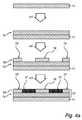
図3a−3dは、本発明に係る発光デバイスを製造する方法の一例を示している。この方法は、(A)例えばガラス又はプラスチックなどの透明基板を準備するステップ(図3a);(B)部分的に透明なアノード層アセンブリを基板上に配設するステップ(図3b);(C)アノード層アセンブリ上に発光層を配設するステップ(図3c);及び(D)発光層上に透明カソード層を配設するステップ(図3d)を有する。この方法において、アノード層アセンブリは、基板に面する透明且つ導電性の第1表面と、不透明な導電材料の第1領域と、透明な電気絶縁材料の第2領域とを備える。また、第1領域は、発光層と直に接触しており、第1表面と発光層との間の電気接触を可能するように構成される。 3a-3d show an example of a method for manufacturing a light emitting device according to the invention. The method includes (A) providing a transparent substrate, such as glass or plastic (FIG. 3a); (B) disposing a partially transparent anode layer assembly on the substrate (FIG. 3b); ) Providing a light emitting layer on the anode layer assembly (FIG. 3c); and (D) providing a transparent cathode layer on the light emitting layer (FIG. 3d). In this method, the anode layer assembly includes a first transparent and conductive surface facing the substrate, a first region of opaque conductive material, and a second region of transparent electrically insulating material. The first region is in direct contact with the light emitting layer and is configured to allow electrical contact between the first surface and the light emitting layer.
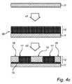
図4a、4b及び4cは、本発明によるアノード層又はアノード層アセンブリを製造するための3つの異なる方法のステップ群を示している。 FIGS. 4a, 4b and 4c show three different method steps for producing an anode layer or anode layer assembly according to the invention.
図4aにおいて、アノード層アセンブリは、(a1)透明導電材料の第1のサブレイヤ19を基板11上に設け;(a2)第1のサブレイヤ19を部分的に覆うように、透明で電気絶縁性の材料の不連続な第2のサブレイヤ20を設け;且つ(a3)上記不連続な第2のサブレイヤによって覆われていない第1のサブレイヤ上の領域に、不透明な導電材料を設けることによって配設される。例えば、これは、例えばITOを基板上に設けた後に、例えばSiO2などの絶縁透明材料の連続層をITO層上に堆積することによって行われ得る。連続した絶縁層を不連続な層に変換するため、連続した層の複数部分が、例えば従来からの有機コーティングなどの保護材料で覆われ、絶縁層の複数部分が、例えば剥離溶液又はプラズマエッチングを用いることによって、エッチングによって除去される。その後、形成された絶縁層の孔内に、例えば電気めっきを用いて、金属が堆積される。上述の保護コーティングは、エッチング工程の直後又は金属の堆積後の何れかに除去されることができる。後者は、構造のうちの不所望の領域での金属堆積が回避され得るという利点をもたらす。また、金属は、表面全体に堆積されて、絶縁領域の頂部から例えば研磨を用いて除去されてもよい。In FIG. 4a, the anode layer assembly comprises (a1) a
図4bにおいて、アノード層アセンブリは、(b1)透明導電材料の第1のサブレイヤ19を設け;(b2)金属又は合金の第2のサブレイヤ20を設け;且つ(b3)第2のサブレイヤを選択的に酸化し、それにより第1及び第2領域17、18を形成することによって配設される。例えば、これは、ITOの第1のサブレイヤを基板上に設け、Alの第2のサブレイヤを付加し、導電性に維持されるべきレイヤアセンブリの部分(すなわち、第1領域)を、印刷又はフォトリソグラフィによって、構造化されたレジストで覆い、そして、覆われていないAl層の部分を下方にITO層まで酸化することでAl2O3の電気絶縁領域を形成することによって行われ得る。その後、レジストは除去され得る。他の例では、第1領域が所望される位置において第2のサブレイヤ上に導電性の不活性材料が設けられる。金属領域17は不透明のままであり、酸化された領域18は酸化によって透明になる。In FIG. 4b, the anode layer assembly is (b1) provided with a
図4cにおいて、アノード層は、(c1)金属又は合金の層12を設け;(c2)層12の表面を所定の深さまで選択的に酸化し、それにより、この酸化で未反応の領域である導電材料の第1領域17を画成するとともに、非導電性の酸化された材料の第2領域(酸化領域)18を形成することによって配設される。この選択酸化は、第2のサブレイヤを部分的に覆い;覆われていない第2のサブレイヤの領域を下方に所定の深さまで酸化することによって行われ得る。金属領域17は不透明なままであり、酸化領域18は上述の酸化によって透明になる。第2領域18の下方の領域の金属層は透明さをもたらすべきである。例えば、第2領域18の下の金属領域は、透明であるのに十分な薄さにされ得る。また、第2領域18の下の金属領域は、この層を光が通過することを可能にするよう、気孔(ポア)若しくは通路(チャンネル)を備えたり、不連続であったりしてもよい。例えば、一部の用途では、アノード層12の総厚の少なくとも30−70%に相当する酸化深さが選択され得る。また、不連続な層が使用される場合、導電領域の網状構造(例えば、格子パターンにされた第1領域構造)によって導電領域が互いに電気的に接続されること、又は、第1領域が個々に電気接続されることが必要とされる。不連続な層が望まれる一部の用途において、アノード層の複数領域の複数部分を下方に基板まで酸化してもよい場合がある。 In FIG. 4c, the anode layer is (c1) provided with a metal or
請求項において、括弧内に置かれた如何なる参照符号も、請求項を限定するものとして解されるべきでない。動詞“有する”及びその活用形の使用は、その請求項中に記載されたもの以外の要素又はステップの存在を排除するものではない。要素の前に置かれる冠詞“a”又は“an”は、その要素が複数存在することを排除するものではない。本発明は、複数の別個の要素を有するハードウェアによって実現されてもよい。複数の手段を列挙するデバイスクレームにおいて、それらの手段のうちの幾つかが、単一且つ同一のハードウェア品目によって具現化されてもよい。特定の複数の手段が互いに異なる従属請求項に記載されているという単なる事実は、それらの手段の組合せが有利に使用され得ないことを指し示すものではない。 In the claims, any reference signs placed between parentheses shall not be construed as limiting the claim. Use of the verb “comprise” and its conjugations does not exclude the presence of elements or steps other than those stated in a claim. The article “a” or “an” preceding an element does not exclude the presence of a plurality of such elements. The present invention may be realized by hardware having a plurality of separate elements. In the device claim enumerating several means, several of these means may be embodied by one and the same item of hardware. The mere fact that certain measures are recited in mutually different dependent claims does not indicate that a combination of these measured cannot be used to advantage.
Claims (9)
Translated fromJapanese− 前記基板上に配置された、部分的に透明なアノード層アセンブリ;
− 前記アノード層アセンブリ上に配置された発光層;及び
− 前記発光層上に配置された透明カソード層;
を有し、
− 前記アノード層アセンブリは、前記基板に面する第1表面と、前記発光層に面し且つ前記第1表面と反対側に位置する第2表面とを有し;
− 前記第1表面は透明導電材料を有し;
− 前記第2表面は、第1領域及び第2領域を有する金属層を有し、前記金属層は、前記第1領域内では非酸化形態にあり且つ前記第2領域内では酸化された少なくとも1つの金属又は合金を有し;
− 前記第1領域は導電性且つ不透明であり;
− 前記第2領域は透明且つ電気絶縁性であり;且つ
− 前記第1領域は、前記発光層と直接的に接触し、前記第1表面と前記発光層との間の電気接触を可能にするように構成されている、
発光デバイス。-Transparent substrates;
-A partially transparentanode layer assembly disposed on the substrate;
A light emitting layer disposed on theanode layer assembly ; and a transparent cathode layer disposed on the light emitting layer;
Have
Theanode layer assembly has a first surface facing the substrate and a second surface facing the light emitting layer and located on the opposite side of the first surface;
-The first surface comprises a transparent conductive material;
The second surface comprises a metal layer having a first region and a second region, the metal layer being in a non-oxidized form in the first region and at least one oxidized in the second region; Having two metals or alloys;
-The first region is electrically conductive and opaque;
-The second region is transparent and electrically insulating; and-the first region is in direct contact with the light-emitting layer, allowing electrical contact between the first surface and the light-emitting layer. Configured as
Light emitting device.
− 前記更なる発光層上に配置された、部分的に透明な、更なるアノード層アセンブリ;
を更に有し、
− 前記更なるアノード層アセンブリは、前記更なる発光層に面する第1表面と、該第1表面と反対側に位置する第2表面とを有し;
− 該第1表面は第1領域及び第2領域を有し;
− 該第1領域は導電性且つ不透明であり;
− 該第2領域は透明且つ電気絶縁性であり;
− 該第2表面は透明導電材料を有し;
− 該第1領域は、前記更なる発光層と直接的に接触し、該第2表面と前記更なる発光層との間の電気接触を可能にするように構成されている、
請求項1に記載の発光デバイス。A further light emitting layer disposed on the cathode layer; and a partially transparent furtheranode layer assembly disposed on the further light emitting layer;
Further comprising
The furtheranode layer assembly has a first surface facing the further light-emitting layer and a second surface located opposite the first surface;
The first surface has a first region and a second region;
-The first region is electrically conductive and opaque;
-The second region is transparent and electrically insulating;
The second surface has a transparent conductive material;
The first region is configured to be in direct contact with the further light emitting layer and to allow electrical contact between the second surface and the further light emitting layer;
The light emitting device according to claim 1.
− 透明基板を準備する工程;
− 前記基板上に、部分的に透明なアノード層アセンブリを設ける工程であり、該アノード層アセンブリは、前記基板に面する透明且つ導電性の第1表面を有し、該アノード層アセンブリは、不透明導電材料の第1領域と、透明電気絶縁材料の第2領域とを備える、工程;
− 前記アノード層アセンブリ上に発光層を設ける工程;及び
− 前記発光層上に透明カソード層を設ける工程;
を有し、
前記第1領域は、前記発光層と直接的に接触し、前記第1表面と前記発光層との間の電気接触を可能にするように構成され、
前記アノード層アセンブリは、
− 透明導電材料の第1のサブレイヤを設け;
− 金属又は合金の第2のサブレイヤを設け;且つ
− 前記第2のサブレイヤを選択酸化し、それにより前記第1領域及び前記第2領域を形成する;
ことによって、あるいは
− 金属又は合金の層を設け;且つ
− 該層の表面を所定深さまで選択酸化し、それにより導電材料の前記第1領域と電気絶縁材料の前記第2領域とを形成する;
ことによって、
の何れかで設けられる、
方法。A method of manufacturing a light emitting device comprising:
-Preparing a transparent substrate;
- on the substrate, a step of providing a partially transparentanode layer assembly, theanode layer assembly has a first surface of the transparent and electrically conductive facing the substrate, theanode layer assembly, opaque Providing a first region of conductive material and a second region of transparent electrically insulating material;
-Providing a light emitting layer on theanode layer assembly ; and-providing a transparent cathode layer on the light emitting layer;
Have
The first region is configured to be in direct contact with the light emitting layer and to allow electrical contact between the first surface and the light emitting layer;
The anode layerassembly is
-Providing a first sublayer of transparent conductive material;
-Providing a second sublayer of metal or alloy; and-selectively oxidizing said second sublayer, thereby forming said first region and said second region;
Or-providing a layer of metal or alloy; and-selectively oxidizing the surface of the layer to a predetermined depth, thereby forming the first region of conductive material and the second region of electrically insulating material;
By
Provided in any of the
Method.
− 前記第2のサブレイヤを部分的に覆い;且つ
− 覆われていない前記第2のサブレイヤの領域を酸化する;
ことによって行われる、請求項7に記載の方法。The selective oxidation is
-Partially covering the second sublayer; and-oxidizing the uncovered region of the second sublayer;
The method according to claim 7, wherein
Applications Claiming Priority (3)
| Application Number | Priority Date | Filing Date | Title |
|---|---|---|---|
| EP10166522 | 2010-06-18 | ||
| EP10166522.2 | 2010-06-18 | ||
| PCT/IB2011/052587WO2011158185A1 (en) | 2010-06-18 | 2011-06-15 | Transparent light emitting device with controlled emission |
Publications (2)
| Publication Number | Publication Date |
|---|---|
| JP2013532363A JP2013532363A (en) | 2013-08-15 |
| JP6058533B2true JP6058533B2 (en) | 2017-01-11 |
Family
ID=44310796
Family Applications (1)
| Application Number | Title | Priority Date | Filing Date |
|---|---|---|---|
| JP2013514821AExpired - Fee RelatedJP6058533B2 (en) | 2010-06-18 | 2011-06-15 | Transparent light emitting device with controlled emission |
Country Status (5)
| Country | Link |
|---|---|
| US (1) | US8766306B2 (en) |
| EP (1) | EP2583328B1 (en) |
| JP (1) | JP6058533B2 (en) |
| CN (1) | CN102934252B (en) |
| WO (1) | WO2011158185A1 (en) |
Families Citing this family (33)
| Publication number | Priority date | Publication date | Assignee | Title |
|---|---|---|---|---|
| KR101084263B1 (en)* | 2009-12-14 | 2011-11-16 | 삼성모바일디스플레이주식회사 | Organic light emitting display |
| JP5758314B2 (en)* | 2012-01-17 | 2015-08-05 | 株式会社東芝 | Organic electroluminescence device and lighting device |
| DE102012202041B4 (en) | 2012-02-10 | 2022-03-17 | Osram Oled Gmbh | Radiation Emitting Device |
| KR101989144B1 (en)* | 2012-04-06 | 2019-06-14 | 삼성디스플레이 주식회사 | Thin layer, method of patterning a thin layer, thin-film transistor substrate and method of manufacturing a thin-film transistor substrate |
| KR20140126439A (en)* | 2013-04-23 | 2014-10-31 | 삼성디스플레이 주식회사 | Method of manufacturing transparent flexible display apparatus and transparent flexible display apparatus using the method |
| KR102212457B1 (en)* | 2013-05-30 | 2021-02-04 | 엘지디스플레이 주식회사 | Organic light emitting display device and manufacturing method of the same |
| EP2808916B1 (en)* | 2013-05-30 | 2018-12-12 | LG Display Co., Ltd. | Method of manufacturing an organic light emitting display device |
| DE102013110666B4 (en) | 2013-09-26 | 2023-05-17 | Pictiva Displays International Limited | Radiation-emitting device and method for producing the same |
| KR102211965B1 (en)* | 2013-10-18 | 2021-02-05 | 삼성디스플레이 주식회사 | Organic light emitting display device |
| KR102122359B1 (en)* | 2013-12-10 | 2020-06-12 | 삼성전자주식회사 | Method for manufacturing light emitting device |
| KR102449804B1 (en)* | 2015-03-02 | 2022-10-04 | 삼성디스플레이 주식회사 | Transparent organic light emitting display apparatus and method of manufacturing the same |
| KR20180075589A (en) | 2015-10-26 | 2018-07-04 | 오티아이 루미오닉스 인크. | A method of patterning a coating on a surface and a device comprising a patterned coating |
| JP7056964B2 (en) | 2016-12-02 | 2022-04-19 | オーティーアイ ルミオニクス インコーポレーテッド | Devices with conductive coatings placed over the radiating region and methods for them |
| JP2020518107A (en) | 2017-04-26 | 2020-06-18 | オーティーアイ ルミオニクス インコーポレーテッドOti Lumionics Inc. | Method for patterning a coating on a surface and device containing the patterned coating |
| CN110832660B (en) | 2017-05-17 | 2023-07-28 | Oti照明公司 | Method for selectively depositing conductive coating on patterned coating and device comprising conductive coating |
| CN107256878A (en)* | 2017-06-09 | 2017-10-17 | 京东方科技集团股份有限公司 | A kind of organic EL display panel and preparation method thereof |
| US11751415B2 (en) | 2018-02-02 | 2023-09-05 | Oti Lumionics Inc. | Materials for forming a nucleation-inhibiting coating and devices incorporating same |
| CN112074966A (en) | 2018-05-07 | 2020-12-11 | Oti照明公司 | Method for providing an auxiliary electrode and device comprising an auxiliary electrode |
| KR20240134065A (en) | 2018-11-23 | 2024-09-05 | 오티아이 루미오닉스 인크. | Optoelectronic device including a light transmissive region |
| CN116456753A (en) | 2019-03-07 | 2023-07-18 | Oti照明公司 | an optoelectronic device |
| KR102831863B1 (en) | 2019-04-18 | 2025-07-10 | 오티아이 루미오닉스 인크. | Material for forming a nucleation-inhibiting coating and device comprising the same |
| CN114072705A (en) | 2019-05-08 | 2022-02-18 | Oti照明公司 | Material for forming nucleation inhibiting coatings and apparatus incorporating the same |
| JP7386556B2 (en) | 2019-06-26 | 2023-11-27 | オーティーアイ ルミオニクス インコーポレーテッド | Optoelectronic devices containing optically transparent regions with applications related to optical diffraction properties |
| US11832473B2 (en) | 2019-06-26 | 2023-11-28 | Oti Lumionics Inc. | Optoelectronic device including light transmissive regions, with light diffraction characteristics |
| CN114342068A (en) | 2019-08-09 | 2022-04-12 | Oti照明公司 | Optoelectronic device containing auxiliary electrodes and partitions |
| CN114651323A (en) | 2019-10-29 | 2022-06-21 | 奥斯兰姆奥普托半导体股份有限两合公司 | Optoelectronic device |
| US12291096B2 (en) | 2019-12-06 | 2025-05-06 | Osram Opto Semiconductors Gmbh | Window or surface of a vehicle comprising at least one optoelectronic component |
| WO2021110331A1 (en) | 2019-12-06 | 2021-06-10 | Osram Opto Semiconductors Gmbh | Optoelectronic arrangement |
| US12040317B2 (en) | 2019-12-06 | 2024-07-16 | Osram Opto Semiconductors Gmbh | Optoelectronic device |
| WO2021110334A1 (en) | 2019-12-06 | 2021-06-10 | Osram Opto Semiconductors Gmbh | Apparatus comprising a carrier with optoelectronic elements and method for manufacturing the apparatus |
| JP7646666B2 (en) | 2019-12-06 | 2025-03-17 | エイエムエス-オスラム インターナショナル ゲーエムベーハー | Optoelectronic Devices |
| KR20220131245A (en) | 2019-12-24 | 2022-09-27 | 오티아이 루미오닉스 인크. | Light emitting device including capping layer and manufacturing method thereof |
| KR20250139404A (en) | 2020-12-07 | 2025-09-23 | 오티아이 루미오닉스 인크. | Patterning a conductive deposited layer using a nucleation inhibiting coating and an underlying metallic coating |
Family Cites Families (16)
| Publication number | Priority date | Publication date | Assignee | Title |
|---|---|---|---|---|
| JPH0693256A (en)* | 1992-09-11 | 1994-04-05 | Fuji Electric Co Ltd | Organic thin-film luminescent element |
| US5902688A (en)* | 1996-07-16 | 1999-05-11 | Hewlett-Packard Company | Electroluminescent display device |
| JP2001005410A (en)* | 1999-06-22 | 2001-01-12 | Toray Ind Inc | Production of display device |
| US6664732B2 (en)* | 2000-10-26 | 2003-12-16 | Semiconductor Energy Laboratory Co., Ltd. | Light emitting device and manufacturing method thereof |
| JP2003162923A (en)* | 2001-11-27 | 2003-06-06 | Matsushita Electric Works Ltd | Transparent conductive substrate and light emitting device |
| JP2003249379A (en) | 2002-02-22 | 2003-09-05 | Takeshi Sakakibara | Surface treatment method for transparent conductive film, transparent conductive film surface-modified by such method, and charge injection type light emitting device having surface-modified transparent conductive film |
| KR100474906B1 (en)* | 2002-06-07 | 2005-03-10 | 엘지전자 주식회사 | Active Matrix Organic Electro-Luminescence Device |
| EP1377133A1 (en) | 2002-06-18 | 2004-01-02 | Alcan Technology & Management Ltd. | Lighting element with luminescent surface and uses thereof |
| CN1802879A (en)* | 2003-07-07 | 2006-07-12 | 先锋株式会社 | Organic electroluminescent display panel and method for manufacturing same |
| TW200515836A (en)* | 2003-10-22 | 2005-05-01 | Hannstar Display Corp | Organic electroluminescent element |
| US7612496B2 (en) | 2005-12-19 | 2009-11-03 | Eastman Kodak Company | OLED device having improved power distribution |
| EP2007843B1 (en) | 2006-04-03 | 2009-12-02 | Philips Intellectual Property & Standards GmbH | Organic electroluminescent device |
| JP2007324233A (en)* | 2006-05-30 | 2007-12-13 | Canon Inc | Organic electroluminescence device and method for manufacturing the same |
| JP2008135259A (en) | 2006-11-28 | 2008-06-12 | Toppan Printing Co Ltd | Organic EL display panel and manufacturing method thereof |
| EP2144290A1 (en) | 2008-07-08 | 2010-01-13 | Nederlandse Organisatie voor toegepast- natuurwetenschappelijk onderzoek TNO | Electronic device and method of manufacturing the same |
| US8310149B2 (en)* | 2008-10-21 | 2012-11-13 | Koninklijke Philips Electronics N.V. | Transparent OLED device employing a mirror layer having a pattern of nontransparent and transparent zones |
- 2011
- 2011-06-15WOPCT/IB2011/052587patent/WO2011158185A1/enactiveApplication Filing
- 2011-06-15CNCN201180030127.2Apatent/CN102934252B/ennot_activeExpired - Fee Related
- 2011-06-15USUS13/704,730patent/US8766306B2/ennot_activeExpired - Fee Related
- 2011-06-15EPEP11729756.4Apatent/EP2583328B1/ennot_activeNot-in-force
- 2011-06-15JPJP2013514821Apatent/JP6058533B2/ennot_activeExpired - Fee Related
Also Published As
| Publication number | Publication date |
|---|---|
| JP2013532363A (en) | 2013-08-15 |
| EP2583328B1 (en) | 2017-08-02 |
| CN102934252A (en) | 2013-02-13 |
| US8766306B2 (en) | 2014-07-01 |
| US20130092914A1 (en) | 2013-04-18 |
| EP2583328A1 (en) | 2013-04-24 |
| CN102934252B (en) | 2016-06-15 |
| WO2011158185A1 (en) | 2011-12-22 |
Similar Documents
| Publication | Publication Date | Title |
|---|---|---|
| JP6058533B2 (en) | Transparent light emitting device with controlled emission | |
| JP6110695B2 (en) | Light emitting device | |
| CN101326655B (en) | A large area organic diode device and a method of manufacturing it | |
| CN102097559B (en) | LED and manufacture method thereof | |
| CN105027315B (en) | For the conductive supporting member of OLED including OLED and its preparation of the supporting member | |
| CN101965654B (en) | The method of Organic Light Emitting Diode, contact device and manufacture Organic Light Emitting Diode | |
| TW200919789A (en) | Opto-electronic semiconductor chip, opto-electronic element and procedure to manufacturing an opto-electronic element | |
| US11522107B2 (en) | Light emitting diode and fabrication method thereof | |
| JP2015503821A (en) | Back-emitting OLED device and method for equalizing the brightness of a back-emitting OLED device | |
| CN111653653B (en) | A light-emitting device and its manufacturing method, and a display panel | |
| US20160079560A1 (en) | Electroconductive Support, OLED Incorporating It, and Manufacture of Same | |
| JP5279914B2 (en) | ORGANIC OPTICAL DEVICE AND METHOD FOR MANUFACTURING ORGANIC OPTICAL DEVICE | |
| US9236582B2 (en) | Back-emitting OLED device | |
| CN104137291A (en) | Backside-emitting oled device | |
| JP7240478B2 (en) | light emitting device | |
| CN114975716B (en) | Micro LED chip and manufacturing method thereof | |
| CN100559537C (en) | Electrode plate of field emission light source and manufacturing method thereof | |
| EP2717313A2 (en) | Large area LED-lighting device | |
| JP2015185339A (en) | organic EL planar light source | |
| JP2023041855A (en) | Organic EL element, organic EL lighting device, and light extraction film that suppresses coloration of organic EL element | |
| KR20070102413A (en) | Thin film type electron source, manufacturing method and thin film type electron source application device | |
| JP2011082175A (en) | Inorganic light-emitting element and method for manufacturing the same |
Legal Events
| Date | Code | Title | Description |
|---|---|---|---|
| A621 | Written request for application examination | Free format text:JAPANESE INTERMEDIATE CODE: A621 Effective date:20140613 | |
| A977 | Report on retrieval | Free format text:JAPANESE INTERMEDIATE CODE: A971007 Effective date:20150408 | |
| A131 | Notification of reasons for refusal | Free format text:JAPANESE INTERMEDIATE CODE: A131 Effective date:20150428 | |
| A601 | Written request for extension of time | Free format text:JAPANESE INTERMEDIATE CODE: A601 Effective date:20150507 | |
| RD02 | Notification of acceptance of power of attorney | Free format text:JAPANESE INTERMEDIATE CODE: A7422 Effective date:20150612 | |
| A521 | Request for written amendment filed | Free format text:JAPANESE INTERMEDIATE CODE: A523 Effective date:20151027 | |
| A02 | Decision of refusal | Free format text:JAPANESE INTERMEDIATE CODE: A02 Effective date:20160411 | |
| A711 | Notification of change in applicant | Free format text:JAPANESE INTERMEDIATE CODE: A711 Effective date:20160426 | |
| A521 | Request for written amendment filed | Free format text:JAPANESE INTERMEDIATE CODE: A523 Effective date:20160810 | |
| A911 | Transfer to examiner for re-examination before appeal (zenchi) | Free format text:JAPANESE INTERMEDIATE CODE: A911 Effective date:20160818 | |
| TRDD | Decision of grant or rejection written | ||
| A01 | Written decision to grant a patent or to grant a registration (utility model) | Free format text:JAPANESE INTERMEDIATE CODE: A01 Effective date:20161109 | |
| A61 | First payment of annual fees (during grant procedure) | Free format text:JAPANESE INTERMEDIATE CODE: A61 Effective date:20161207 | |
| R150 | Certificate of patent or registration of utility model | Ref document number:6058533 Country of ref document:JP Free format text:JAPANESE INTERMEDIATE CODE: R150 | |
| R250 | Receipt of annual fees | Free format text:JAPANESE INTERMEDIATE CODE: R250 | |
| R250 | Receipt of annual fees | Free format text:JAPANESE INTERMEDIATE CODE: R250 | |
| LAPS | Cancellation because of no payment of annual fees |