JP6055270B2 - Solid-state imaging device, manufacturing method thereof, and camera - Google Patents
Solid-state imaging device, manufacturing method thereof, and cameraDownload PDFInfo
- Publication number
- JP6055270B2 JP6055270B2JP2012237270AJP2012237270AJP6055270B2JP 6055270 B2JP6055270 B2JP 6055270B2JP 2012237270 AJP2012237270 AJP 2012237270AJP 2012237270 AJP2012237270 AJP 2012237270AJP 6055270 B2JP6055270 B2JP 6055270B2
- Authority
- JP
- Japan
- Prior art keywords
- pixel
- light
- substrate
- film
- imaging device
- Prior art date
- Legal status (The legal status is an assumption and is not a legal conclusion. Google has not performed a legal analysis and makes no representation as to the accuracy of the status listed.)
- Active
Links
Images


Classifications
- H—ELECTRICITY
- H10—SEMICONDUCTOR DEVICES; ELECTRIC SOLID-STATE DEVICES NOT OTHERWISE PROVIDED FOR
- H10F—INORGANIC SEMICONDUCTOR DEVICES SENSITIVE TO INFRARED RADIATION, LIGHT, ELECTROMAGNETIC RADIATION OF SHORTER WAVELENGTH OR CORPUSCULAR RADIATION
- H10F39/00—Integrated devices, or assemblies of multiple devices, comprising at least one element covered by group H10F30/00, e.g. radiation detectors comprising photodiode arrays
- H10F39/80—Constructional details of image sensors
- H10F39/806—Optical elements or arrangements associated with the image sensors
- H10F39/8067—Reflectors
- H—ELECTRICITY
- H10—SEMICONDUCTOR DEVICES; ELECTRIC SOLID-STATE DEVICES NOT OTHERWISE PROVIDED FOR
- H10F—INORGANIC SEMICONDUCTOR DEVICES SENSITIVE TO INFRARED RADIATION, LIGHT, ELECTROMAGNETIC RADIATION OF SHORTER WAVELENGTH OR CORPUSCULAR RADIATION
- H10F39/00—Integrated devices, or assemblies of multiple devices, comprising at least one element covered by group H10F30/00, e.g. radiation detectors comprising photodiode arrays
- H10F39/011—Manufacture or treatment of image sensors covered by group H10F39/12
- H10F39/024—Manufacture or treatment of image sensors covered by group H10F39/12 of coatings or optical elements
- H—ELECTRICITY
- H10—SEMICONDUCTOR DEVICES; ELECTRIC SOLID-STATE DEVICES NOT OTHERWISE PROVIDED FOR
- H10F—INORGANIC SEMICONDUCTOR DEVICES SENSITIVE TO INFRARED RADIATION, LIGHT, ELECTROMAGNETIC RADIATION OF SHORTER WAVELENGTH OR CORPUSCULAR RADIATION
- H10F39/00—Integrated devices, or assemblies of multiple devices, comprising at least one element covered by group H10F30/00, e.g. radiation detectors comprising photodiode arrays
- H10F39/10—Integrated devices
- H10F39/12—Image sensors
- H10F39/199—Back-illuminated image sensors
- H—ELECTRICITY
- H10—SEMICONDUCTOR DEVICES; ELECTRIC SOLID-STATE DEVICES NOT OTHERWISE PROVIDED FOR
- H10F—INORGANIC SEMICONDUCTOR DEVICES SENSITIVE TO INFRARED RADIATION, LIGHT, ELECTROMAGNETIC RADIATION OF SHORTER WAVELENGTH OR CORPUSCULAR RADIATION
- H10F39/00—Integrated devices, or assemblies of multiple devices, comprising at least one element covered by group H10F30/00, e.g. radiation detectors comprising photodiode arrays
- H10F39/80—Constructional details of image sensors
- H10F39/805—Coatings
Landscapes
- Solid State Image Pick-Up Elements (AREA)
- Transforming Light Signals Into Electric Signals (AREA)
Description
Translated fromJapanese本発明は、固体撮像装置、その製造方法、およびカメラに関する。 The present invention relates to a solid-state imaging device, a manufacturing method thereof, and a camera.
裏面照射型の固体撮像装置において、光電変換部が設けられる基板は、厚さが、例えば3μm程度であり、入射光のうち波長の大きい成分(例えば、緑色光や赤色光)は表面側へ透過してしまう。 In the back-illuminated solid-state imaging device, the substrate on which the photoelectric conversion unit is provided has a thickness of about 3 μm, for example, and a component having a large wavelength (for example, green light or red light) is transmitted to the front side. Resulting in.
特許文献1には、光電変換素子111を有する基板(素子層110)を覆うように反射膜140が配された構造が開示されている。特許文献1の構造によると、基板を透過する光は反射膜140によって反射され、光電変換素子111において光電変換されるため、光感度を向上させることができる。
特許文献1の構造によると、基板を透過する光は、一律に反射膜140によって光電変換素子111に向けて反射される。即ち、例えば、緑色光や赤色光が青色光を検知すべき画素(青色画素)に混入した場合には、この青色画素において緑色光や赤色光が検知されてしまう。このことは、取得すべき画像の品質を低下させうる。 According to the structure of
本発明の目的は、固体撮像装置における隣接画素間の混色の防止に有利な技術を提供することにある。 An object of the present invention is to provide a technique advantageous for preventing color mixture between adjacent pixels in a solid-state imaging device.
本発明の一つの側面は固体撮像装置にかかり、前記固体撮像装置は、第1波長の光を検出するための第1の画素と、前記第1波長より波長が短い第2波長の光を検出するための第2の画素とを有する固体撮像装置であって、互いに反対の側に配された第1面及び第2面を有し、前記第1の画素および前記第2の画素のそれぞれに対応する光電変換部が形成された基板と、前記基板の前記第1面の側に配され、前記第1の画素および前記第2の画素のそれぞれに対応するマイクロレンズを含む光学系と、前記基板の前記第2面の側に配され、前記第1の画素および前記第2の画素のそれぞれに対応する光吸収部と、を備え、前記固体撮像装置は、前記第1の画素に対応する前記光吸収部と前記基板との間に配された第1部分と、前記第2の画素に対応する前記光吸収部と前記基板との間に配された第2部分とをさらに備えており、前記第1部分は前記第1波長の光の反射率が前記第2部分よりも大きく、前記第1部分は、前記基板の側から前記光吸収部の側に向かって、前記基板よりも屈折率が小さく誘電性を有する第1膜と、前記第1膜よりも屈折率が大きい第2膜と、前記第2膜よりも屈折率が小さい絶縁部分と、を含み、前記第2部分は、前記基板の側から前記光吸収部の側に向かって、前記第1膜と前記絶縁部分とを含み、前記第1膜の光学膜厚および前記第2膜の光学膜厚は、前記第1波長の1/4の±30%の範囲内である、ことを特徴とする。
One aspect of the present invention relates to a solid-state imaging device, and the solid-state imaging device detects a first pixel for detecting light having a first wavelength and light having a second wavelength shorter than the first wavelength. A solid-state imaging device having a first surface and a second surface disposed on opposite sides of each of the first pixel and the second pixel. A substrate on which a corresponding photoelectric conversion unit is formed; an optical system that is disposed on the first surface side of the substrate and includes microlenses corresponding to the first pixel and the second pixel; A light absorbing portion disposed on the second surface side of the substrate and corresponding to each of the first pixel and the second pixel, wherein the solid-state imaging device corresponds to the first pixel A first portion disposed between the light absorbing portion and the substrate; and the second pixel. And corresponding the light absorbing portion, further comprising a disposed a second portion between said substrate and said first portion reflectance of light of the first wavelength ismuch larger than the said secondportion, The first portion includes a first film having a refractive index smaller than that of the substrate and having a dielectric property from the substrate side toward the light absorbing portion, and a second film having a refractive index larger than that of the first film. A film and an insulating portion having a refractive index smaller than that of the second film, and the second portion includes the first film and the insulating portion from the substrate side toward the light absorbing portion. The optical film thickness of the first film and the optical film thickness of the second film are in a range of ± 30% of ¼ of the first wavelength .
本発明によれば、固体撮像装置における隣接画素間の混色の防止に有利である。 The present invention is advantageous for preventing color mixture between adjacent pixels in a solid-state imaging device.
(第1実施形態)
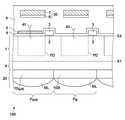
図1乃至3を参照しながら、第1実施形態の固体撮像装置100を説明する。図1は、固体撮像装置100の断面構造を模式的に例示している。固体撮像装置100は、複数の画素Pを有しており、基板1と光学系20と光吸収部30とを備え、裏面照射型の構造を有する。ここでは、説明の簡易化のため、2つの画素P(PG/RおよびPB)を例示している。(First embodiment)
The solid-
基板1は、互いに反対の側に配された第1面S1及び第2面S2を有し、複数の画素Pのそれぞれに対応する複数の光電変換部PDが形成されている。例えば、基板1はP型不純物を含むシリコンで構成され、光電変換部PDは基板1にN型の不純物が注入されて形成される。また、基板1には、例えば、光電変換部PDから画素信号を読み出すためのMOSトランジスタが設けられ、図1には、当該MOSトランジスタのゲート酸化膜2およびゲート電極3を例示している。ゲート酸化膜2は、例えばSiO2で構成される。ゲート電極3は、例えばポリシリコンで構成される。また、これらの上には、絶縁性の部材を堆積することにより、絶縁部分6(層間絶縁層)が設けられ、その内部に電源供給用ないし信号伝達用の配線パターン(不図示)が配されうる。The
光学系20は、基板1の第1面の側(S1側)に各画素Pに対応して設けられた複数のマイクロレンズMLを含む。また、光学系20はカラーフィルタ10(10G/Rおよび10B)を有し、複数の画素Pが波長の異なる光を検知することが可能な構成になっている。複数の画素Pは、第1波長の光を検出するための第1種類の画素PG/Rと、第1波長より波長が短い第2波長の光を検出するための第2種類の画素PBと、を含む。本実施形態では、第1波長の光として赤色光(λR=610〜780[nm]程度)や緑色光(λG=500〜570[nm]程度)を例示し、第2波長の光として青色光(λB=430〜480[nm]程度)を例示する。The
カラーフィルタ10G/Rが配された画素を画素PG/Rと示し、カラーフィルタ10Bが配された画素を画素PBと示す。カラーフィルタ10G/Rは赤色光ないし緑色光を透過させ、カラーフィルタ10Bは青色光を透過させる。即ち、画素PG/Rは、波長(λG/R)の長い緑色光ないし赤色光を検知し、画素PBは、波長(λB)の短い青色光を検知する。また、光学系20は、光を透過させる材料で構成された平坦化層9を含んでもよく、基板1の裏面側を平坦化するために形成されうる。A pixel in which the color filter 10G / R is arranged is referred to as a pixel PG / R, and a pixel in which the color filter 10B is arranged is referred to as a pixel PB. The color filter 10G / R transmits red light or green light, and the color filter 10B transmits blue light. That is, the pixel PG / R detects green light or red light having a long wavelength (λG / R ), and the pixel PB detects blue light having a short wavelength (λB ). Further, the
光吸収部30は、光を吸収する部材で構成され、第2面の側(S2側)に各画素Pに対応してそれぞれ設けられる。光吸収部30は絶縁部分6の内部に設けられうる。光吸収部30は、例えば2つの部材が積層されて構成されてもよく、基板1に近い側から順に、光を吸収するための部材で構成された部分8と、導電性を有する部材で構成された金属部分7とで構成されうる。光吸収部30は、例えば、信号を伝達するための配線パターンが配された配線層に設けられうる。金属部分7は、例えば、アルミニウムや銅などの金属部材で構成された配線パターンでもよく、制御信号用ないし信号読出用の信号線を形成しうる。部分8は、例えばTiN(チタンナイトライド)を用いて、金属配線7の原子が拡散することを防止するための層として設けられてもよい。 The
固体撮像装置100は、第1部分41と第2部分42とをさらに備える。第1部分41は、画素PG/Rのそれぞれにおいて、光吸収部30と基板1との間に配される。第2部分42は、画素PBのそれぞれにおいて、光吸収部30と基板1との間に配される。第1部分41は、赤色光ないし緑色光に対する反射率が第2部分42よりも大きくなるように設けられている。第1部分41は、例えば、基板1の側から光吸収部30の側に向かって、誘電性を有する誘電体膜4(第1誘電膜)と、誘電性を有する高屈折率膜5(第2誘電膜)と、絶縁部分6と、を含む。一方、第2部分42は、例えば、基板1の側から光吸収部30の側に向かって、誘電体膜4と絶縁部分6とを含む。つまり、画素PG/Rには高屈折率膜5が配されているが、画素PBには高屈折率膜5が配されていない。The solid-
誘電体膜4は基板1よりも屈折率が小さい。高屈折率膜5は誘電体膜4よりも屈折率が大きい。絶縁部分6は基板1よりも屈折率が小さい。また、絶縁部分6は誘電体膜4よりも屈折率が小さい若しくは等しい。また、誘電体膜4および高屈折率膜5は、それらの光学膜厚のそれぞれが、赤色光ないし緑色光の波長の1/4の±30%の範囲内になるように設けられるとよい。これらの光学膜厚は、好ましくは、当該波長の1/4の±20%、さらに好ましくは、±10%の範囲内であるとよい。具体的には、誘電体膜4は、例えばSi3N4で構成され(屈折率1.9〜2.2程度)、膜厚は50〜80nm程度とすればよい。高屈折率膜5は、例えばポリシリコンで構成され(屈折率3.9〜4.2)、膜厚は30〜45nm程度とすればよい。絶縁部分6は、例えばSiO2等の誘電性の部材で構成され(屈折率1.4〜1.5)、厚さは400nm〜1000nm(1000nm以上でもよい)とすればよい。以上のような構成により、赤色光ないし緑色光に対する反射率は第1部分41の方が第2部分42よりも大きくなるように設計できる。The
以下、固体撮像装置100の構成による作用・効果について、図2を参照しながら述べる。基板1の屈折率をn1とし、誘電体膜4の屈折率をn4とし、誘電体膜4の厚さをd4とし、高屈折率層膜5の屈折率をn5とし、高屈折率層膜5の厚さをd5とし、絶縁部分6の屈折率をn6とする。本実施形態では、n1>n4>n6、n5>n4、n5>n6の関係が成立している場合について考える。なお、光を吸収する物質による消衰係数k(複素屈折率の虚数成分)は、実数成分よりも十分に小さいものとする。 Hereinafter, operations and effects of the configuration of the solid-
裏面照射型の固体撮像装置は、一般に、表面照射型の固体撮像装置よりも基板の厚さが薄く、例えば3μm程度の厚さである。よって、固体撮像装置100において、基板1の第1面S1側から入射した光のうち波長の長い赤色光ないし緑色光は、基板1の第2面S2側に達しうる。ここでは、例として、画素PG/Rに垂直に入射した光が、隣接画素PBに混入した場合の波長λG/Rの混色光について考える。In general, a back-illuminated solid-state imaging device has a thinner substrate than a front-illuminated solid-state imaging device, for example, a thickness of about 3 μm. Therefore, in the solid-
図2は、第1面S1側から入射して第2面S2側に到達した光の反射ないし透過の様子を説明するための第1部分41および第2部分42の拡大図である。基板1から基板1と誘電体膜4との界面S14に到達した透過波の振幅をA14とし、界面S14において基板1に向かって反射された光の反射波成分をR14とする。誘電体膜4から誘電体膜4と高屈折率膜5との界面S45に到達した透過波の振幅をA45とし、界面S45において誘電体膜4に向かって反射された光の反射波成分をR45とする。高屈折率膜5から高屈折率膜5と絶縁部分6との界面S56に到達した透過波の振幅をA56とし、界面S56において高屈折率膜5に向かって反射された光の反射波成分をR56とする。誘電体膜4から誘電体膜4と絶縁部分6との界面S46に到達した透過波の振幅をA46とし、界面S46において誘電体膜4に向かって反射された光の反射波成分をR46とする。なお、界面S45等を代表して「界面S」と称する。FIG. 2 is an enlarged view of the
反射波は、屈折率の高い部材から低い部材に到達して反射される場合は位相のずれは生じず、屈折率の低い部材から高い部材に到達して反射される場合は位相が180°ずれる。このことは、フレネルの式を用いると、R14=A14×(n1−n4)/(n1+n4)>0と表せる。同様にして、R45=A45×(n4−n5)/(n4+n5)<0と表せ、R56=A56×(n5−n6)/(n5+n6)>0と表せ、R46=A46×(n4−n6)/(n4+n6)>0と表せる。以下では、理解を容易にするため、A45=A56=A46=A14とする。この仮定(ないし近似)は、各界面Sにおける反射率が1よりも十分に小さい場合に成り立ち、本実施形態の構造においては妥当な近似といえる。When the reflected wave reaches the low member from the high refractive index and is reflected, no phase shift occurs. When the reflected wave reaches the high member from the low refractive index and is reflected, the phase is shifted by 180 °. . This can be expressed as R14 = A14 × (n1−n4) / (n1 + n4)> 0 using the Fresnel equation. Similarly, R45 = A45 × (n4-n5) / (n4 + n5) <0, R56 = A56 × (n5-n6) / (n5 + n6)> 0, and R46 = A46 × It can be expressed as (n4-n6) / (n4 + n6)> 0. Hereinafter, in order to facilitate understanding, it is assumed that A45 = A56 = A46 = A14 . This assumption (or approximation) holds when the reflectance at each interface S is sufficiently smaller than 1, and can be said to be a reasonable approximation in the structure of this embodiment.
まず、図2の右側に示された画素PBについて述べる。画素PBに第1面S1側から垂直に入射した光(波長λB)は、基板1においてほぼ100%吸収される。一方、画素PG/Rからの混色光(波長λG/R)は、第2面S2に到達しうる。光の反射を効果的に防止する条件からn4=(n1×n6)1/2と設計すると、R14=R46となる。また、d4×n4=λG/R/4、即ち、d4が波長λG/Rの1/4の光路長になるように設計すると、界面S46における反射光の位相は、界面S14に戻ってきたときに180°ずれる。よって、これらの反射光成分は、正負が逆になって打ち消し合い、即ち、第2部分42は、混色光(波長λG/R)を透過させる。現実に、n4=(n1×n6)1/2にすることは難しいが、n1>n4>n6、d4×n4=λG/R/4になるように設計することで、反射光成分R14と反射光成分R46とは打ち消し合う。このようにして、第2部分42においては、波長λG/Rの光の反射を防止し、光を透過させる。First, the pixel PB shown on the right side of FIG. 2 will be described. The light (wavelength λB ) perpendicularly incident on the pixel PB from the
次に、図2の左側に示された画素PG/Rについて述べる。基板1、誘電体膜4および高屈折率膜5のそれぞれの屈折率について、n1>n4、n5>n4の関係が成り立つとき、R14とR45とは正負が逆になる。反射光成分R45<0であり、即ち、位相が180°ずれている。また、d4×n4=λG/R/4と設計されている。よって、これら2つの反射光は強めあう。さらに、高屈折率膜5の厚さをd5×n5=λG/R/4、即ち、d5を波長λG/Rの1/4の光路長になるように設計すると、界面S56における反射光R56の位相は、界面S14に到達したときには360°ずれている。結果として、3つの反射光は強めあう。このようにして、第1部分41においては、波長λG/Rの光を反射させる。Next, the pixel PG/ R shown on the left side of FIG. 2 will be described. For each refractive index of the
高屈折率膜5の屈折率n5を大きくすると上述の反射効率を高くすることができる。高屈折率膜5には、例えばポリシリコンが用いられうるが、ポリシリコンそのものによる光の吸収を小さくするように、ポリシリコンのドーパント密度を調整するとよい(例えば、1×10¹⁹[cm−3]以下)。Increasing the refractive index n5 of the high
図3は、固体撮像装置100の製造方法を説明するための図である。図3(a)は、基板1の上に、ゲート酸化膜2およびゲート電極3を形成した後、誘電性部材4’、ポリシリコン5’、および誘電性部材12’を堆積して、さらにフォトレジストパターン13を形成した後の構造を示している。ゲート電極3を形成した後の基板の全面を覆うように誘電性部材4’、ポリシリコン5’、誘電性部材12’をそれぞれ順に形成する。その後、さらにフォトレジストを形成し、公知の半導体製造プロセスによってパターニングして、フォトレジストパターン13を形成する。 FIG. 3 is a diagram for explaining a method for manufacturing the solid-
図3(b)は、フォトレジストパターン13をマスクとして誘電性部材12’をエッチングによりパターニングし、誘電性の部分12が形成された後の構造を示している。図3(c)は、誘電性の部分12をマスクとしてポリシリコン5’をエッチングによりパターニングし、高屈折率膜5が形成された後の構造を示している。その後は、公知の半導体製造プロセスによって、絶縁部分6と金属配線7とを含む配線領域を形成すればよい。誘電性部材12’(ないし誘電性の部分12)には、絶縁部分6と同じ部材を用いてもよいが、その屈折率n12は、少なくとも高屈折率膜5の屈折率n5よりも小さくする。ここでは、ポリシリコン5’をパターニングするときのマスクとして誘電性の部分12を用いる場合を例示したが、通常の露光工程と同様にレジストパターンを形成して行ってもよい。 FIG. 3B shows the structure after the
以上では、画素PBにおける各部材の屈折率について関係式n1>n4>n6と、画素PG/Rにおける各部材の屈折率について関係式n1>n4かつn5>n4と、d4×n4=λG/R/4と、d5×n5=λG/R/4と設定した場合について検討した。この構成により、画素PBにおいては波長λG/Rの光(混色光)を透過させ、画素PG/Rにおいては波長λG/Rの光(入射光)を反射させる。これにより、画素PG/Rにおいては光感度を向上させ、画素PBにおいては、隣接画素からの混色を低減する。In the above, the relational expression n1>n4> n6 for the refractive index of each member in the pixel PB , the relational expressions n1> n4 and n5> n4 for the refractive index of each member in the pixel PG / R , and d4 × n4 = λ.The case where G / R / 4 and d5 × n5 = λG / R / 4 were set was examined. With this configuration, the pixel PB transmits light having a wavelength λG / R (mixed color light), and the pixel PG / R reflects light having a wavelength λG / R (incident light). Thereby, the photosensitivity is improved in the pixel PG / R , and the color mixture from the adjacent pixels is reduced in the pixel PB.
また、固体撮像装置100は、透過した混色光が光吸収部30によって吸収されて基板1に向かって再び反射されないような構成を採っている。光吸収部30について、部分8は、金属部分7よりも底面積が大きくなるように設けられてもよい。これにより、絶縁部分6の領域における光の乱反射が防止され、迷光を防ぎうる。例えば、部分8は、金属部分7の側面を覆うように設けられてもよい。 Further, the solid-
また、既に述べたように、誘電体膜4および高屈折率膜5の光学膜厚は、赤色光ないし緑色光の波長の1/4の±30%の範囲内になるように設計すればよい。光学膜厚は、上記構造のパラメータに応じて適宜変更してもよく、例えば、画素Pのピッチ、各構成部材の厚さや屈折率を考慮して、斜入射光に対して効果が得られるように調整してもよい。 Further, as described above, the optical film thickness of the
さらに、上述の構造は、本実施形態のように、基板1、誘電体膜4、高屈折率層膜5、絶縁部分6等、誘電性の部材および半導体を用いて構成されうる。よって、基板1への汚染源となりうる金属部材を用いないで構成することができる。よって、光電変換部PD表面に金属が混入することを防止し、その結果、暗電流によるノイズを低減することもできる。以上、本実施形態によると、固体撮像装置100の光感度を向上させ、混色を低減し、ノイズを低減することが可能であり、固体撮像装置100の高品質化に有利である。 Furthermore, the above-described structure can be configured using a dielectric member and a semiconductor such as the
(第2実施形態)
以下では、第2実施形態について説明する。第1実施形態では、n4>n6の場合を示したが、例えば誘電体膜4としてSiO2を用いて、関係式n4≦n6が成り立つように構成してもよい。この場合、固体撮像装置100は、画素PBに入射した混色光(波長λG/R)の界面S14における反射を防止せず、当該混色光の界面S14における透過率は、第1実施形態よりも低い。一方、画素PG/Rにおいては、反射光振幅R14およびR45が第1実施形態より大きく、入射光(波長λG/R)の界面S14および界面S45における光反射の効果は第1実施形態よりも大きい。よって、本実施形態の構造は、斜入射光や迷光による混色の低減よりも、光感度の向上を優先できる場合において好適である。このことは、例えば、基板1の厚さが薄い場合や、波長がより長い光についての感度を向上させたい場合や、隣接画素間の混色に対する対策が別途なされる場合に好適である。よって、本実施形態によっても、第1実施形態と同様の効果が得られる。(Second Embodiment)
Below, 2nd Embodiment is described. Although the case of n4> n6 is shown in the first embodiment, for example, SiO2 may be used as the
以上、2つの実施形態を述べたが、本発明はこれらに限られるものではなく、目的、状態、用途及び機能その他の仕様に応じて、適宜、変更が可能であり、他の実施形態によっても為されうる。例えば、第1ないし第2実施形態において、誘電体膜4は、1種類の誘電性部材で構成される必要はなく、例えば、2種類の誘電性部材を用いて2層構造にしてもよいし、3層以上の構造にしてもよい。この場合、2層(ないし3層以上の)構造の誘電体膜4の合計の光学膜厚について、前述のような設計をすればよい。2層構造の場合、2種類の部材のうちの屈折率が高い方(n41とする)については、n41<n1、n41<n5となり、平均屈折率n4aveがn4ave>n6となるようにすれば、第1実施形態と同様の効果が得られる。また、n41<n1、n41<n5、n4ave<n6となるようにすれば、第2実施形態と同様の効果が得られる。また、実際に多く採られる構造として、2種類の部材のうち屈折率の小さい方の部材は、絶縁部分6と同じ材料としてもよい。誘電体膜4の形成は、各画素に形成されるトランジスタの各々のゲート電極が形成された後に為されればよい。Although two embodiments have been described above, the present invention is not limited to these embodiments, and can be changed as appropriate according to the purpose, state, application, function, and other specifications. Can be done. For example, in the first or second embodiment, the
また、第1ないし第2実施形態では、誘電体膜4が単層構成の場合について例示したが、厳密には、例えば、SiO2で構成されるゲート酸化膜と、Si3N4等の誘電性部材とで構成された2層構造となる。しかし、ゲート酸化膜の厚さは、例えば数[nm]程度であり、誘電体膜4の厚さより十分に小さく、上述の関係式においてゲート酸化膜の厚さは考慮しなくてもよい。In the first and second embodiments, the case where the
以上では、カメラに含まれる固体撮像装置について述べたが、カメラの概念には、撮影を主目的とする装置のみならず、撮影機能を補助的に備える装置(例えば、パーソナルコンピュータ、携帯端末)も含まれる。カメラは、上記の実施形態として例示された本発明に係る固体撮像装置と、この固体撮像装置から出力される信号を処理する処理部とを含みうる。この処理部は、例えば、A/D変換器、および、このA/D変換器から出力されるデジタルデータを処理するプロセッサを含みうる。 In the above, the solid-state imaging device included in the camera has been described. However, the concept of the camera includes not only a device mainly used for shooting but also a device (for example, a personal computer or a portable terminal) provided with a shooting function as an auxiliary. included. The camera can include a solid-state imaging device according to the present invention exemplified as the above-described embodiment, and a processing unit that processes a signal output from the solid-state imaging device. The processing unit may include, for example, an A / D converter and a processor that processes digital data output from the A / D converter.
Claims (10)
Translated fromJapanese互いに反対の側に配された第1面及び第2面を有し、前記第1の画素および前記第2の画素のそれぞれに対応する光電変換部が形成された基板と、
前記基板の前記第1面の側に配され、前記第1の画素および前記第2の画素のそれぞれに対応するマイクロレンズを含む光学系と、
前記基板の前記第2面の側に配され、前記第1の画素および前記第2の画素のそれぞれに対応する光吸収部と、を備え、
前記固体撮像装置は、前記第1の画素に対応する前記光吸収部と前記基板との間に配された第1部分と、前記第2の画素に対応する前記光吸収部と前記基板との間に配された第2部分とをさらに備えており、前記第1部分は前記第1波長の光の反射率が前記第2部分よりも大きく、
前記第1部分は、前記基板の側から前記光吸収部の側に向かって、前記基板よりも屈折率が小さく誘電性を有する第1膜と、前記第1膜よりも屈折率が大きい第2膜と、前記第2膜よりも屈折率が小さい絶縁部分と、を含み、
前記第2部分は、前記基板の側から前記光吸収部の側に向かって、前記第1膜と前記絶縁部分とを含み、
前記第1膜の光学膜厚および前記第2膜の光学膜厚は、前記第1波長の1/4の±30%の範囲内である、
ことを特徴とする固体撮像装置。A solid-state imaging device having a first pixel for detecting light of a first wavelength and a second pixel for detecting light of a second wavelength shorter than the first wavelength,
A substrate having a first surface and a second surface disposed on opposite sides of each other, and a photoelectric conversion unit corresponding to each of the first pixel and the second pixel;
An optical system disposed on the first surface side of the substrate and including a microlens corresponding to each of the first pixel and the second pixel;
A light absorbing portion disposed on the second surface side of the substrate and corresponding to each of the first pixel and the second pixel;
The solid-state imaging device includes: a first portion disposed between the light absorption unit corresponding to the first pixel and the substrate; and the light absorption unit corresponding to the second pixel and the substrate. further comprising a second portion disposed between said first portionmuch larger than the said second portion reflectance of light of the firstwavelength,
The first portion includes a first film having a refractive index smaller than that of the substrate and having a dielectric property from the substrate side toward the light absorbing portion, and a second film having a refractive index larger than that of the first film. A film, and an insulating portion having a refractive index smaller than that of the second film,
The second portion includes the first film and the insulating portion from the substrate side toward the light absorbing portion side,
The optical film thickness of the first film and the optical film thickness of the second film are within a range of ± 30% of ¼ of the first wavelength .
A solid-state imaging device.
ことを特徴とする請求項1に記載の固体撮像装置。The first film is made of silicon nitride, and a gate electrode of a first transistor is disposed between the first film and the substrate in the first pixel, and in the second pixel, A gate electrode of a second transistor is disposed between the first film and the substrate.
The solid-state imaging device according to claim 1.
ことを特徴とする請求項1または請求項2に記載の固体撮像装置。The second layer is a solid-state imaging device according to claim1 or claim 2, characterized in that it is composed of polysilicon.
ことを特徴とする請求項1乃至3のいずれか1項に記載の固体撮像装置。The light absorbing portion is configured by laminating a member for absorbing light and a conductive member in order from the side close to the substrate, and a portion configured by a member for absorbing the light Is a bottom area larger than the portion made of the conductive member,
The solid-state imaging device according to any one of claims 1 to 3.
ことを特徴とする請求項4に記載の固体撮像装置。The portion made of the member for absorbing light covers the side surface of the portion made of the conductive member,
The solid-state imaging device according to claim 4.
ことを特徴とする請求項4または請求項5に記載の固体撮像装置。6. The solid-state imaging device according to claim 4, wherein the portion made of the member for absorbing light is made of titanium nitride.
ことを特徴とする請求項1乃至6のいずれか1項に記載の固体撮像装置。An optical film thickness of the region from the substrate for the previousSL first pixel to the light absorbing portion, and the optical thickness of the previousSL region from the substrate for thesecond pixel to the light absorbing portion, to each other The solid-state imaging device according to claim 1, wherein the solid-state imaging device is different.
ことを特徴とする請求項1乃至7のいずれか1項に記載の固体撮像装置。Wherein the first wavelength light is green light, the light of the secondwavelength solid-state imaging device according to any one of claims 1 to 7, characterized in that ablue color light.
前記固体撮像装置から出力される信号を処理する処理部と、
を備えることを特徴とするカメラ。A solid-state imaging device according to any one of claims 1 to 8,
A processing unit for processing a signal output from the solid-state imaging device;
A camera comprising:
前記固体撮像装置は、互いに反対の側に配された第1面及び第2面を有し、前記第1の画素および前記第2の画素のそれぞれに対応する光電変換部が形成された基板と、前記基板の前記第1面の側に配され、前記第1の画素および前記第2の画素のそれぞれに対応するマイクロレンズを含む光学系と、前記基板の前記第2面の側に配され、前記第1の画素および前記第2の画素のそれぞれに対応する光吸収部と、を備え、
前記固体撮像装置の製造方法は、
前記第1の画素および前記第2の画素のそれぞれに対して、前記基板の上に誘電性を有する第1誘電膜を形成する工程と、
前記第1の画素に対して、前記第1誘電膜の上に誘電性を有する第2誘電膜を形成する工程と、
前記第1の画素および前記第2の画素のそれぞれに対して、前記第1誘電膜および前記第2誘電膜を覆うように絶縁性を有する絶縁部分を堆積する工程と、を含み、
前記第1誘電膜は前記基板よりも屈折率が小さく、前記第2誘電膜は前記第1誘電膜よりも屈折率が大きく、前記絶縁部分は前記第2誘電膜よりも屈折率が小さく、前記第1誘電膜の光学膜厚および前記第2誘電膜の光学膜厚は、前記第1波長の1/4の±30%の範囲内である、
ことを特徴とする固体撮像装置の製造方法。
A method for manufacturing a solid-state imaging device, comprising: a first pixel for detecting light having a first wavelength; and a second pixel for detecting light having a second wavelength shorter than the first wavelength. ,
The solid-state imaging device has a first surface and a second surface arranged on opposite sides, and a substrate on which a photoelectric conversion unit corresponding to each of the first pixel and the second pixel is formed; An optical system that is disposed on the first surface side of the substrate and includes a microlens corresponding to each of the first pixel and the second pixel, and is disposed on the second surface side of the substrate. A light absorbing portion corresponding to each of the first pixel and the second pixel,
The manufacturing method of the solid-state imaging device is:
Forming a dielectric first dielectric film on the substrate for each of the first pixel and the second pixel;
Forming a second dielectric film having dielectric properties on the first dielectric film for the first pixel;
Depositing an insulating portion having an insulating property so as to cover the first dielectric film and the second dielectric film for each of the first pixel and the second pixel;
The first dielectric film has a lower refractive index than the substrate, the second dielectric film has a higher refractive index than the first dielectric film, the insulating portion has a lower refractive index than the second dielectric film, The optical film thickness of the first dielectric film and the optical film thickness of the second dielectric film are within a range of ± 30% of ¼ of the first wavelength.
A method of manufacturing a solid-state imaging device.
Priority Applications (3)
| Application Number | Priority Date | Filing Date | Title |
|---|---|---|---|
| JP2012237270AJP6055270B2 (en) | 2012-10-26 | 2012-10-26 | Solid-state imaging device, manufacturing method thereof, and camera |
| US14/046,474US8970769B2 (en) | 2012-10-26 | 2013-10-04 | Solid-state imaging apparatus, method of manufacturing the same, and camera |
| CN201310496051.3ACN103794615B (en) | 2012-10-26 | 2013-10-22 | Solid-state imaging apparatus, its manufacture method, and camera |
Applications Claiming Priority (1)
| Application Number | Priority Date | Filing Date | Title |
|---|---|---|---|
| JP2012237270AJP6055270B2 (en) | 2012-10-26 | 2012-10-26 | Solid-state imaging device, manufacturing method thereof, and camera |
Publications (3)
| Publication Number | Publication Date |
|---|---|
| JP2014086702A JP2014086702A (en) | 2014-05-12 |
| JP2014086702A5 JP2014086702A5 (en) | 2015-12-03 |
| JP6055270B2true JP6055270B2 (en) | 2016-12-27 |
Family
ID=50546775
Family Applications (1)
| Application Number | Title | Priority Date | Filing Date |
|---|---|---|---|
| JP2012237270AActiveJP6055270B2 (en) | 2012-10-26 | 2012-10-26 | Solid-state imaging device, manufacturing method thereof, and camera |
Country Status (3)
| Country | Link |
|---|---|
| US (1) | US8970769B2 (en) |
| JP (1) | JP6055270B2 (en) |
| CN (1) | CN103794615B (en) |
Families Citing this family (23)
| Publication number | Priority date | Publication date | Assignee | Title |
|---|---|---|---|---|
| US9121759B2 (en)* | 2013-09-09 | 2015-09-01 | Heptagon Micro Optics Pte. Ltd. | Arrangements for detecting light of different wavelength at different angles |
| JP6274567B2 (en) | 2014-03-14 | 2018-02-07 | キヤノン株式会社 | Solid-state imaging device and imaging system |
| JP2015177034A (en) | 2014-03-14 | 2015-10-05 | キヤノン株式会社 | Solid-state imaging device, manufacturing method thereof, and camera |
| US10204943B2 (en) | 2016-08-10 | 2019-02-12 | Canon Kabushiki Kaisha | Image sensor, method of manufacturing the same, and camera with pixel including light waveguide and insulation film |
| JP6552479B2 (en) | 2016-12-28 | 2019-07-31 | キヤノン株式会社 | Solid-state imaging device and imaging system |
| JP6982977B2 (en) | 2017-04-24 | 2021-12-17 | キヤノン株式会社 | Manufacturing method of solid-state image sensor |
| CN107680980A (en)* | 2017-09-29 | 2018-02-09 | 德淮半导体有限公司 | Imaging sensor |
| JP6953263B2 (en) | 2017-10-05 | 2021-10-27 | キヤノン株式会社 | Solid-state image sensor and imaging system |
| JP2019114642A (en)* | 2017-12-22 | 2019-07-11 | キヤノン株式会社 | Solid state image sensor, electronic equipment and transport equipment |
| WO2019159561A1 (en)* | 2018-02-13 | 2019-08-22 | ソニーセミコンダクタソリューションズ株式会社 | Solid-state imaging element, electronic device, and method for manufacturing solid-state imaging element |
| JP7108421B2 (en) | 2018-02-15 | 2022-07-28 | キヤノン株式会社 | Imaging device and imaging system |
| KR102614907B1 (en)* | 2018-04-04 | 2023-12-19 | 삼성전자주식회사 | Image sensor and method to produce image sensor |
| JP7134781B2 (en) | 2018-08-17 | 2022-09-12 | キヤノン株式会社 | Photoelectric conversion device and imaging system |
| JP2020068289A (en)* | 2018-10-24 | 2020-04-30 | キヤノン株式会社 | Photoelectric conversion device, imaging system, moving body, and semiconductor chip for stacking |
| US11503234B2 (en) | 2019-02-27 | 2022-11-15 | Canon Kabushiki Kaisha | Photoelectric conversion device, imaging system, radioactive ray imaging system, and movable object |
| CN109950266A (en)* | 2019-03-26 | 2019-06-28 | 德淮半导体有限公司 | Imaging sensor and the method for forming imaging sensor |
| WO2021215299A1 (en)* | 2020-04-21 | 2021-10-28 | ソニーセミコンダクタソリューションズ株式会社 | Imaging element and imaging device |
| JP7652543B2 (en) | 2020-07-29 | 2025-03-27 | キヤノン株式会社 | Photoelectric conversion device |
| JP7656409B2 (en)* | 2020-08-24 | 2025-04-03 | タワー パートナーズ セミコンダクター株式会社 | Solid-state imaging device |
| JP7534902B2 (en) | 2020-09-23 | 2024-08-15 | キヤノン株式会社 | Photoelectric conversion device, imaging device, semiconductor device, and photoelectric conversion system |
| JP2023023218A (en) | 2021-08-04 | 2023-02-16 | キヤノン株式会社 | Photoelectric conversion device |
| JP2024004306A (en) | 2022-06-28 | 2024-01-16 | キヤノン株式会社 | Photoelectric conversion device |
| JP2024017294A (en) | 2022-07-27 | 2024-02-08 | キヤノン株式会社 | Photoelectric conversion device |
Family Cites Families (44)
| Publication number | Priority date | Publication date | Assignee | Title |
|---|---|---|---|---|
| JP2003152217A (en)* | 2001-11-16 | 2003-05-23 | Matsushita Electric Ind Co Ltd | Semiconductor device with built-in light receiving element |
| JP2004071817A (en)* | 2002-08-06 | 2004-03-04 | Canon Inc | Imaging sensor |
| JP2004104203A (en)* | 2002-09-05 | 2004-04-02 | Toshiba Corp | Solid-state imaging device |
| JP2005005540A (en)* | 2003-06-12 | 2005-01-06 | Sharp Corp | Solid-state imaging device and manufacturing method thereof |
| JP2005142510A (en)* | 2003-11-10 | 2005-06-02 | Matsushita Electric Ind Co Ltd | Solid-state imaging device and manufacturing method thereof |
| JP2006054262A (en)* | 2004-08-10 | 2006-02-23 | Sony Corp | Solid-state imaging device |
| US7453109B2 (en)* | 2004-09-03 | 2008-11-18 | Canon Kabushiki Kaisha | Solid-state image sensor and imaging system |
| EP1816677A1 (en)* | 2004-09-09 | 2007-08-08 | Matsushita Electric Industrial Co., Ltd. | Solid-state image pickup element |
| US7592645B2 (en)* | 2004-12-08 | 2009-09-22 | Canon Kabushiki Kaisha | Photoelectric conversion device and method for producing photoelectric conversion device |
| US7456384B2 (en)* | 2004-12-10 | 2008-11-25 | Sony Corporation | Method and apparatus for acquiring physical information, method for manufacturing semiconductor device including array of plurality of unit components for detecting physical quantity distribution, light-receiving device and manufacturing method therefor, and solid-state imaging device and manufacturing method therefor |
| JP4826111B2 (en) | 2005-03-17 | 2011-11-30 | ソニー株式会社 | Solid-state imaging device, manufacturing method of solid-state imaging device, and image photographing apparatus |
| JP4469781B2 (en)* | 2005-07-20 | 2010-05-26 | パナソニック株式会社 | Solid-state imaging device and manufacturing method thereof |
| US8013409B2 (en) | 2005-09-27 | 2011-09-06 | Canon Kabushiki Kaisha | Photoelectric conversion device and fabrication method therefor |
| CN101086546A (en)* | 2006-06-09 | 2007-12-12 | 鸿富锦精密工业(深圳)有限公司 | Lens module and camera module |
| KR100745991B1 (en)* | 2006-08-11 | 2007-08-06 | 삼성전자주식회사 | Image sensor and its manufacturing method |
| US7656000B2 (en)* | 2007-05-24 | 2010-02-02 | Taiwan Semiconductor Manufacturing Company, Ltd. | Photodetector for backside-illuminated sensor |
| US8133768B2 (en)* | 2007-05-31 | 2012-03-13 | Nthdegree Technologies Worldwide Inc | Method of manufacturing a light emitting, photovoltaic or other electronic apparatus and system |
| TW200913238A (en)* | 2007-06-04 | 2009-03-16 | Sony Corp | Optical member, solid state imaging apparatus, and manufacturing method |
| KR100876613B1 (en)* | 2008-05-27 | 2008-12-31 | 한국철강 주식회사 | Tandem Thin Film Silicon Solar Cell and Manufacturing Method Thereof |
| JP2010016056A (en) | 2008-07-01 | 2010-01-21 | Canon Inc | Photoelectric conversion device |
| JP5406537B2 (en) | 2009-01-13 | 2014-02-05 | キヤノン株式会社 | Photoelectric conversion device, imaging system, and method of manufacturing photoelectric conversion device |
| US9543356B2 (en)* | 2009-03-10 | 2017-01-10 | Globalfoundries Inc. | Pixel sensor cell including light shield |
| FR2946777B1 (en)* | 2009-06-12 | 2011-07-22 | Commissariat Energie Atomique | DEVICE FOR DETECTING AND / OR EMITTING ELECTROMAGNETIC RADIATION AND METHOD FOR MANUFACTURING SUCH A DEVICE |
| JP2011014733A (en)* | 2009-07-02 | 2011-01-20 | Toshiba Corp | Solid-state image pickup device |
| JP5489570B2 (en) | 2009-07-27 | 2014-05-14 | キヤノン株式会社 | Photoelectric conversion device and imaging system |
| US8896077B2 (en)* | 2009-10-23 | 2014-11-25 | The Board Of Trustees Of The Leland Stanford Junior University | Optoelectronic semiconductor device and method of fabrication |
| US8252624B2 (en)* | 2010-01-18 | 2012-08-28 | Applied Materials, Inc. | Method of manufacturing thin film solar cells having a high conversion efficiency |
| US8368157B2 (en)* | 2010-04-06 | 2013-02-05 | Aptina Imaging Coporation | Backside illumination image sensors with reflective light guides |
| JP5717357B2 (en) | 2010-05-18 | 2015-05-13 | キヤノン株式会社 | Photoelectric conversion device and camera |
| JP2012042665A (en)* | 2010-08-18 | 2012-03-01 | Sony Corp | Optical function element and imaging device |
| JP2012094719A (en)* | 2010-10-27 | 2012-05-17 | Sony Corp | Solid-state imaging device, method of manufacturing the same and electronic device |
| JP5767465B2 (en) | 2010-12-15 | 2015-08-19 | キヤノン株式会社 | Solid-state imaging device, manufacturing method thereof, and camera |
| JP5810575B2 (en)* | 2011-03-25 | 2015-11-11 | ソニー株式会社 | Solid-state imaging device, manufacturing method thereof, and electronic apparatus |
| JP2012238632A (en)* | 2011-05-10 | 2012-12-06 | Sony Corp | Solid-state imaging device, method of manufacturing the same, and electronic apparatus |
| JP2013038091A (en)* | 2011-08-03 | 2013-02-21 | Toshiba Corp | Solid-state image sensor and manufacturing method therefor |
| JP6029266B2 (en)* | 2011-08-09 | 2016-11-24 | キヤノン株式会社 | Imaging device, imaging system, and manufacturing method of imaging device |
| JP2013077740A (en)* | 2011-09-30 | 2013-04-25 | Sony Corp | Solid-state imaging device, method for manufacturing solid-state imaging device, and electronic apparatus |
| JP2013093553A (en) | 2011-10-04 | 2013-05-16 | Canon Inc | Photoelectric conversion device and manufacturing method therefor, and photoelectric conversion system |
| US8680454B2 (en)* | 2011-12-01 | 2014-03-25 | Omnivision Technologies, Inc. | Backside-illuminated (BSI) pixel including light guide |
| US8786769B2 (en)* | 2011-12-15 | 2014-07-22 | Blackberry Limited | Camera module having protruding lens barrel |
| US9040913B2 (en)* | 2011-12-19 | 2015-05-26 | Nanohmics, Inc. | Wavelength-selective, integrated resonance detector for electromagnetic radiation |
| JP5774502B2 (en)* | 2012-01-12 | 2015-09-09 | 株式会社東芝 | Solid-state imaging device |
| JP5710526B2 (en)* | 2012-03-14 | 2015-04-30 | 株式会社東芝 | Solid-state imaging device and method for manufacturing solid-state imaging device |
| US8835961B2 (en)* | 2012-08-02 | 2014-09-16 | Intermolecular, Inc. | Index-matched insulators |
- 2012
- 2012-10-26JPJP2012237270Apatent/JP6055270B2/enactiveActive
- 2013
- 2013-10-04USUS14/046,474patent/US8970769B2/enactiveActive
- 2013-10-22CNCN201310496051.3Apatent/CN103794615B/enactiveActive
Also Published As
| Publication number | Publication date |
|---|---|
| JP2014086702A (en) | 2014-05-12 |
| US8970769B2 (en) | 2015-03-03 |
| CN103794615B (en) | 2016-09-07 |
| US20140118602A1 (en) | 2014-05-01 |
| CN103794615A (en) | 2014-05-14 |
Similar Documents
| Publication | Publication Date | Title |
|---|---|---|
| JP6055270B2 (en) | Solid-state imaging device, manufacturing method thereof, and camera | |
| KR102633229B1 (en) | Imaging device and method of manufacturing the imaging device, imaging device, and method of manufacturing the imaging device | |
| CN103765584B (en) | Solid State Image Sensor | |
| KR100874954B1 (en) | Rear receiving image sensor | |
| JP4826111B2 (en) | Solid-state imaging device, manufacturing method of solid-state imaging device, and image photographing apparatus | |
| JP4075678B2 (en) | Solid-state image sensor | |
| US9093345B2 (en) | Solid-state imaging apparatus and imaging system | |
| Teranishi et al. | Evolution of optical structure in image sensors | |
| US20130037902A1 (en) | Image sensing device, image sensing system, and method for manufacturing image sensing device | |
| US20100244168A1 (en) | Solid-state imaging device | |
| JP2014130890A (en) | Photoelectric conversion device | |
| US20120050600A1 (en) | Unit pixel array and image sensor having the same | |
| US20080254565A1 (en) | Method for fabricating semiconductor image sensor | |
| CN108807443B (en) | An image sensor with an embedded color filter array | |
| KR20130088705A (en) | Methods and apparatus for an improved reflectivity optical grid for image sensors | |
| JP7598975B2 (en) | Method for simplifying image sensor and image signal processing device | |
| JP5866248B2 (en) | Solid-state image sensor | |
| JP2011142330A (en) | Solid-state image sensor, camera module and electronic equipment module | |
| JP2011151421A (en) | Solid-state image sensor, method of manufacturing the same, and imaging device | |
| JP4779304B2 (en) | Solid-state image sensor, camera module, and electronic device module | |
| TW201104856A (en) | Solid-state imaging device, camera, electronic apparatus, and method for manufacturing solid-state imaging device | |
| JP2009290089A (en) | Solid state imaging device and method for manufacturing therefor | |
| JP5282797B2 (en) | Solid-state imaging device, manufacturing method of solid-state imaging device, and image photographing apparatus | |
| JP6080494B2 (en) | Solid-state imaging device and imaging system | |
| CN107680980A (en) | Imaging sensor |
Legal Events
| Date | Code | Title | Description |
|---|---|---|---|
| A521 | Request for written amendment filed | Free format text:JAPANESE INTERMEDIATE CODE: A523 Effective date:20151015 | |
| A621 | Written request for application examination | Free format text:JAPANESE INTERMEDIATE CODE: A621 Effective date:20151015 | |
| A977 | Report on retrieval | Free format text:JAPANESE INTERMEDIATE CODE: A971007 Effective date:20160816 | |
| A131 | Notification of reasons for refusal | Free format text:JAPANESE INTERMEDIATE CODE: A131 Effective date:20160822 | |
| A521 | Request for written amendment filed | Free format text:JAPANESE INTERMEDIATE CODE: A523 Effective date:20161012 | |
| TRDD | Decision of grant or rejection written | ||
| A01 | Written decision to grant a patent or to grant a registration (utility model) | Free format text:JAPANESE INTERMEDIATE CODE: A01 Effective date:20161104 | |
| A61 | First payment of annual fees (during grant procedure) | Free format text:JAPANESE INTERMEDIATE CODE: A61 Effective date:20161202 | |
| R151 | Written notification of patent or utility model registration | Ref document number:6055270 Country of ref document:JP Free format text:JAPANESE INTERMEDIATE CODE: R151 |