JP6055239B2 - DIE BONDING DEVICE, DIE PICKUP DEVICE, AND DIE PICKUP METHOD - Google Patents
DIE BONDING DEVICE, DIE PICKUP DEVICE, AND DIE PICKUP METHODDownload PDFInfo
- Publication number
- JP6055239B2 JP6055239B2JP2012188339AJP2012188339AJP6055239B2JP 6055239 B2JP6055239 B2JP 6055239B2JP 2012188339 AJP2012188339 AJP 2012188339AJP 2012188339 AJP2012188339 AJP 2012188339AJP 6055239 B2JP6055239 B2JP 6055239B2
- Authority
- JP
- Japan
- Prior art keywords
- die
- push
- dicing tape
- diaphragm
- cylinder
- Prior art date
- Legal status (The legal status is an assumption and is not a legal conclusion. Google has not performed a legal analysis and makes no representation as to the accuracy of the status listed.)
- Active
Links
Images


Classifications
- H—ELECTRICITY
- H01—ELECTRIC ELEMENTS
- H01L—SEMICONDUCTOR DEVICES NOT COVERED BY CLASS H10
- H01L21/00—Processes or apparatus adapted for the manufacture or treatment of semiconductor or solid state devices or of parts thereof
- H01L21/67—Apparatus specially adapted for handling semiconductor or electric solid state devices during manufacture or treatment thereof; Apparatus specially adapted for handling wafers during manufacture or treatment of semiconductor or electric solid state devices or components ; Apparatus not specifically provided for elsewhere
- H01L21/67005—Apparatus not specifically provided for elsewhere
- H01L21/67011—Apparatus for manufacture or treatment
- H01L21/67121—Apparatus for making assemblies not otherwise provided for, e.g. package constructions
- H—ELECTRICITY
- H05—ELECTRIC TECHNIQUES NOT OTHERWISE PROVIDED FOR
- H05K—PRINTED CIRCUITS; CASINGS OR CONSTRUCTIONAL DETAILS OF ELECTRIC APPARATUS; MANUFACTURE OF ASSEMBLAGES OF ELECTRICAL COMPONENTS
- H05K13/00—Apparatus or processes specially adapted for manufacturing or adjusting assemblages of electric components
- H05K13/02—Feeding of components
- H—ELECTRICITY
- H01—ELECTRIC ELEMENTS
- H01L—SEMICONDUCTOR DEVICES NOT COVERED BY CLASS H10
- H01L21/00—Processes or apparatus adapted for the manufacture or treatment of semiconductor or solid state devices or of parts thereof
- H01L21/02—Manufacture or treatment of semiconductor devices or of parts thereof
- H01L21/04—Manufacture or treatment of semiconductor devices or of parts thereof the devices having potential barriers, e.g. a PN junction, depletion layer or carrier concentration layer
- H01L21/50—Assembly of semiconductor devices using processes or apparatus not provided for in a single one of the groups H01L21/18 - H01L21/326 or H10D48/04 - H10D48/07 e.g. sealing of a cap to a base of a container
- H01L21/52—Mounting semiconductor bodies in containers
- H—ELECTRICITY
- H01—ELECTRIC ELEMENTS
- H01L—SEMICONDUCTOR DEVICES NOT COVERED BY CLASS H10
- H01L21/00—Processes or apparatus adapted for the manufacture or treatment of semiconductor or solid state devices or of parts thereof
- H01L21/67—Apparatus specially adapted for handling semiconductor or electric solid state devices during manufacture or treatment thereof; Apparatus specially adapted for handling wafers during manufacture or treatment of semiconductor or electric solid state devices or components ; Apparatus not specifically provided for elsewhere
- H01L21/67005—Apparatus not specifically provided for elsewhere
- H01L21/67011—Apparatus for manufacture or treatment
- H01L21/67132—Apparatus for placing on an insulating substrate, e.g. tape
- H—ELECTRICITY
- H01—ELECTRIC ELEMENTS
- H01L—SEMICONDUCTOR DEVICES NOT COVERED BY CLASS H10
- H01L2221/00—Processes or apparatus adapted for the manufacture or treatment of semiconductor or solid state devices or of parts thereof covered by H01L21/00
- H01L2221/67—Apparatus for handling semiconductor or electric solid state devices during manufacture or treatment thereof; Apparatus for handling wafers during manufacture or treatment of semiconductor or electric solid state devices or components; Apparatus not specifically provided for elsewhere
- H01L2221/683—Apparatus for handling semiconductor or electric solid state devices during manufacture or treatment thereof; Apparatus for handling wafers during manufacture or treatment of semiconductor or electric solid state devices or components; Apparatus not specifically provided for elsewhere for supporting or gripping
- H01L2221/68304—Apparatus for handling semiconductor or electric solid state devices during manufacture or treatment thereof; Apparatus for handling wafers during manufacture or treatment of semiconductor or electric solid state devices or components; Apparatus not specifically provided for elsewhere for supporting or gripping using temporarily an auxiliary support
- H01L2221/68381—Details of chemical or physical process used for separating the auxiliary support from a device or wafer
- Y—GENERAL TAGGING OF NEW TECHNOLOGICAL DEVELOPMENTS; GENERAL TAGGING OF CROSS-SECTIONAL TECHNOLOGIES SPANNING OVER SEVERAL SECTIONS OF THE IPC; TECHNICAL SUBJECTS COVERED BY FORMER USPC CROSS-REFERENCE ART COLLECTIONS [XRACs] AND DIGESTS
- Y10—TECHNICAL SUBJECTS COVERED BY FORMER USPC
- Y10S—TECHNICAL SUBJECTS COVERED BY FORMER USPC CROSS-REFERENCE ART COLLECTIONS [XRACs] AND DIGESTS
- Y10S156/00—Adhesive bonding and miscellaneous chemical manufacture
- Y10S156/918—Delaminating processes adapted for specified product, e.g. delaminating medical specimen slide
- Y10S156/93—Semiconductive product delaminating, e.g. delaminating emiconductive wafer from underlayer
- Y10S156/931—Peeling away backing
- Y10S156/932—Peeling away backing with poking during delaminating, e.g. jabbing release sheet backing to remove wafer
- Y—GENERAL TAGGING OF NEW TECHNOLOGICAL DEVELOPMENTS; GENERAL TAGGING OF CROSS-SECTIONAL TECHNOLOGIES SPANNING OVER SEVERAL SECTIONS OF THE IPC; TECHNICAL SUBJECTS COVERED BY FORMER USPC CROSS-REFERENCE ART COLLECTIONS [XRACs] AND DIGESTS
- Y10—TECHNICAL SUBJECTS COVERED BY FORMER USPC
- Y10S—TECHNICAL SUBJECTS COVERED BY FORMER USPC CROSS-REFERENCE ART COLLECTIONS [XRACs] AND DIGESTS
- Y10S156/00—Adhesive bonding and miscellaneous chemical manufacture
- Y10S156/934—Apparatus having delaminating means adapted for delaminating a specified article
- Y10S156/941—Means for delaminating semiconductive product
- Y10S156/943—Means for delaminating semiconductive product with poking delaminating means, e.g. jabbing means
- Y—GENERAL TAGGING OF NEW TECHNOLOGICAL DEVELOPMENTS; GENERAL TAGGING OF CROSS-SECTIONAL TECHNOLOGIES SPANNING OVER SEVERAL SECTIONS OF THE IPC; TECHNICAL SUBJECTS COVERED BY FORMER USPC CROSS-REFERENCE ART COLLECTIONS [XRACs] AND DIGESTS
- Y10—TECHNICAL SUBJECTS COVERED BY FORMER USPC
- Y10T—TECHNICAL SUBJECTS COVERED BY FORMER US CLASSIFICATION
- Y10T156/00—Adhesive bonding and miscellaneous chemical manufacture
- Y10T156/11—Methods of delaminating, per se; i.e., separating at bonding face
- Y10T156/1126—Using direct fluid current against work during delaminating
- Y10T156/1132—Using vacuum directly against work during delaminating
- Y—GENERAL TAGGING OF NEW TECHNOLOGICAL DEVELOPMENTS; GENERAL TAGGING OF CROSS-SECTIONAL TECHNOLOGIES SPANNING OVER SEVERAL SECTIONS OF THE IPC; TECHNICAL SUBJECTS COVERED BY FORMER USPC CROSS-REFERENCE ART COLLECTIONS [XRACs] AND DIGESTS
- Y10—TECHNICAL SUBJECTS COVERED BY FORMER USPC
- Y10T—TECHNICAL SUBJECTS COVERED BY FORMER US CLASSIFICATION
- Y10T156/00—Adhesive bonding and miscellaneous chemical manufacture
- Y10T156/11—Methods of delaminating, per se; i.e., separating at bonding face
- Y10T156/1168—Gripping and pulling work apart during delaminating
- Y10T156/1179—Gripping and pulling work apart during delaminating with poking during delaminating [e.g., jabbing, etc.]
- Y—GENERAL TAGGING OF NEW TECHNOLOGICAL DEVELOPMENTS; GENERAL TAGGING OF CROSS-SECTIONAL TECHNOLOGIES SPANNING OVER SEVERAL SECTIONS OF THE IPC; TECHNICAL SUBJECTS COVERED BY FORMER USPC CROSS-REFERENCE ART COLLECTIONS [XRACs] AND DIGESTS
- Y10—TECHNICAL SUBJECTS COVERED BY FORMER USPC
- Y10T—TECHNICAL SUBJECTS COVERED BY FORMER US CLASSIFICATION
- Y10T156/00—Adhesive bonding and miscellaneous chemical manufacture
- Y10T156/17—Surface bonding means and/or assemblymeans with work feeding or handling means
- Y10T156/1702—For plural parts or plural areas of single part
- Y10T156/1744—Means bringing discrete articles into assembled relationship
- Y—GENERAL TAGGING OF NEW TECHNOLOGICAL DEVELOPMENTS; GENERAL TAGGING OF CROSS-SECTIONAL TECHNOLOGIES SPANNING OVER SEVERAL SECTIONS OF THE IPC; TECHNICAL SUBJECTS COVERED BY FORMER USPC CROSS-REFERENCE ART COLLECTIONS [XRACs] AND DIGESTS
- Y10—TECHNICAL SUBJECTS COVERED BY FORMER USPC
- Y10T—TECHNICAL SUBJECTS COVERED BY FORMER US CLASSIFICATION
- Y10T156/00—Adhesive bonding and miscellaneous chemical manufacture
- Y10T156/19—Delaminating means
- Y10T156/1928—Differential fluid pressure delaminating means
- Y10T156/1944—Vacuum delaminating means [e.g., vacuum chamber, etc.]
- Y—GENERAL TAGGING OF NEW TECHNOLOGICAL DEVELOPMENTS; GENERAL TAGGING OF CROSS-SECTIONAL TECHNOLOGIES SPANNING OVER SEVERAL SECTIONS OF THE IPC; TECHNICAL SUBJECTS COVERED BY FORMER USPC CROSS-REFERENCE ART COLLECTIONS [XRACs] AND DIGESTS
- Y10—TECHNICAL SUBJECTS COVERED BY FORMER USPC
- Y10T—TECHNICAL SUBJECTS COVERED BY FORMER US CLASSIFICATION
- Y10T156/00—Adhesive bonding and miscellaneous chemical manufacture
- Y10T156/19—Delaminating means
- Y10T156/1978—Delaminating bending means
- Y10T156/1983—Poking delaminating means
Landscapes
- Engineering & Computer Science (AREA)
- Manufacturing & Machinery (AREA)
- Microelectronics & Electronic Packaging (AREA)
- Physics & Mathematics (AREA)
- Condensed Matter Physics & Semiconductors (AREA)
- General Physics & Mathematics (AREA)
- Computer Hardware Design (AREA)
- Power Engineering (AREA)
- Container, Conveyance, Adherence, Positioning, Of Wafer (AREA)
- Die Bonding (AREA)
Description
Translated fromJapanese本発明は、ダイ(半導体チップ)を基板上に搭載するためにダイボンディング装置に関し、特に、ダイをピックアップするダイピックアップ装置及びダイピックアップ方法に関する。 The present invention relates to a die bonding apparatus for mounting a die (semiconductor chip) on a substrate, and more particularly to a die pickup apparatus and a die pickup method for picking up a die.
一般に、ダイと呼ばれる半導体チップを、例えば、配線基板やリードフレームなど(以下、総称して基板と称する)の表面に搭載するダイボンディング装置においては、一般的に、コレット等の吸着ノズルを用いてダイを基板上に搬送し、押付力を付与すると共に、接合材を加熱することによりボンディングを行うという動作(作業)が繰り返して行われる。 In general, in a die bonding apparatus in which a semiconductor chip called a die is mounted on the surface of a wiring board, a lead frame, or the like (hereinafter collectively referred to as a board), a suction nozzle such as a collet is generally used. The operation (work) of transferring the die onto the substrate, applying a pressing force, and performing bonding by heating the bonding material is repeatedly performed.
ダイボンディング装置によるダイボンディング工程の中には、ウェハから分割されたダイを剥離する剥離工程がある。剥離工程では、ダイシングテープ裏面から突き上げユニットによってダイを突き上げて、ダイピックアップ装置に保持されたダイシングテープから、1個ずつ剥離し、コレット等の吸着ノズル(吸着治具)を使って基板上に搬送する。
例えば、特許文献1によれば、ダイシングテープに貼り付けられた複数のダイのうち剥離対象のダイを突き上げてダイシングテープから剥離する際に、ダイの周辺部のうちの所定部におけるダイシングテープを突き上げて剥離起点を形成し、その後、所定部以外部分のダイシングテープを突き上げてダイをダイシングテープから剥離している。In the die bonding process by the die bonding apparatus, there is a peeling process for peeling the divided dies from the wafer. In the peeling process, the die is pushed up from the back side of the dicing tape by the pushing unit, peeled off one by one from the dicing tape held in the die pick-up device, and transported onto the substrate using a suction nozzle (suction jig) such as a collet. To do.
For example, according to
ところで、近年、半導体装置の高密度実装を推進する目的で、パッケージの薄型化が進められている。特に、メモリカードの配線基板上に複数枚のダイを三次元的に実装する積層パッケージが実用化されている。このような積層パッケージを組み立てるに際しては、パッケージ厚の増加を防ぐために、ダイの厚さを10μm程度まで薄くすることが要求される。
しかし、従来は、突き上げユニットは金属等の固体であった。例えば、初期の突き上げユニットでは、ダイシングテープを突き破ってダイを突き上げるために、突き上げユニットのダイと接触する先端部分は、金属等の固体で先端が尖ったニードルが多かった。そして、ダイの破損を少なくするため、先端部分は複数のニードルを設けるようになり、近年は、先端部分が複数のコマ状の部品となり、更に段階的にダイを押し上げて、ダイの破損を少なくするようになってきている。
例えば、特許文献1のように、ダイシングテープを突き上げてダイをダイシングテープから剥離する場合に、固体による突き上げのために、ダイシングテープに貼り付けられた複数のダイのうち剥離対象のダイを突き上げてダイシングテープから剥離する際に、ダイの周辺部のうちの所定部におけるダイシングテープを突き上げて剥離起点を形成し、その後、所定部以外部分のダイシングテープを突き上げてダイをダイシングテープから剥離するようにしている。By the way, in recent years, packages have been made thinner for the purpose of promoting high-density mounting of semiconductor devices. In particular, a stacked package in which a plurality of dies are three-dimensionally mounted on a wiring board of a memory card has been put into practical use. When assembling such a stacked package, it is required to reduce the die thickness to about 10 μm in order to prevent an increase in the package thickness.
However, conventionally, the push-up unit has been a solid such as metal. For example, in the initial push-up unit, in order to pierce the dicing tape and push up the die, the tip portion that comes into contact with the die of the push-up unit often has a needle with a sharp tip made of a solid such as metal. In order to reduce the damage to the die, the tip portion is provided with a plurality of needles. In recent years, the tip portion becomes a plurality of piece-like parts, and the die is pushed up step by step to reduce the damage to the die. Is starting to do.
For example, as in
上述の突き上げユニットでは、固体の構造物によってダイを突き上げるため、ダイの厚さ、大きさ(チップサイズ:ダイのサイズ)、ダイシングテープとダイの接着強度等の条件によって、ダイに無理な力が加わる可能性がある。この結果、突き上げによって、ダイの破損(欠け、割れ等)が発生していた。
本発明の目的は、上記のような問題に鑑み、ダイの破損が少ないダイピックアップ方法、及び、確実にダイボンディング可能で、信頼性が高いダイボンディング装置を提供することにある。In the above-described push-up unit, the die is pushed up by a solid structure, so that an excessive force is applied to the die depending on conditions such as die thickness, size (chip size: die size), and dicing tape-die bonding strength. There is a possibility of joining. As a result, the die was damaged (chips, cracks, etc.) due to the pushing up.
In view of the above-described problems, an object of the present invention is to provide a die pick-up method with less die breakage and a die bonding apparatus that can reliably perform die bonding and has high reliability.
上記の目的を達成するために、本発明のダイボンディング装置は、基板を搬送するワーク供給・搬送部と、搬送されてきた前記基板にダイをボンディングするボンディング部と、前記ダイを有するウェハを供給するウェハ供給部と、各機器を制御する制御部とから構成されるダイボンディング装置において、前記ウェハ供給部は、前記ダイをダイシングテープから剥離するためにダイシングテープの下方から突き上げる突き上げユニットを有し、前記突き上げユニットは、前記ダイシングテープを真空吸着する吸着孔部、流体または粉体を封じ込めた弾性体から成り前記ダイシングテープを突き上げる突き上げ部、前記突き上げ部に圧力をかけるシリンダ、及び、前記制御部の制御により前記シリンダ内の圧力を変更するためのエアーを供給するエアー供給手段を有し、前記突き上げ部は、前記ダイシングテープ側に配置された第1のダイアフラムと、前記エアー供給手段側に配置された第2のダイアフラムを備え、前記第1のダイアフラムと前記第2のダイアフラムの間に前記流体または粉体が封じ込められており、前記シリンダは、前記第2のダイアフラムにより、前記流体または粉体の部屋である上部の突き上げ部と、前記エアーの部屋である下部のシリンダに隔離されていることを第1の特徴とする。In order to achieve the above object, a die bonding apparatus of the present invention supplies a workpiece supply / conveyance unit for conveying a substrate, a bonding unit for bonding a die to the substrate that has been conveyed, and a wafer having the die. In a die bonding apparatus comprising a wafer supply unit that performs control and a control unit that controls each device, the wafer supply unit has a push-up unit that pushes up from below the dicing tape in order to peel the die from the dicing tape The push-up unit includes a suction hole portion that vacuum-sucks the dicing tape, a push-up portion that pushes up the dicing tape, and a cylinder that applies pressure to the push-up portion, and the control unit. Supplying air to change the pressure in the cylinder by controlling Thathave a air supplymeans, the push-up portion includes a first diaphragm disposed on the dicing tape side, a second diaphragm disposed in the air supply means side, the said first diaphragm The fluid or powder is contained between the second diaphragms, and the cylinder is an upper push-up portion which is a chamber of the fluid or powder and the air chamber by the second diaphragm. The first featureis thatit is isolated by a lower cylinder .
上記本発明の第1の特徴のダイボンディング装置において、前記突き上げ部は、前記シリンダの内部に設けられ、前記シリンダの圧力に応じて、前記弾性体が変形して、前記ダイを前記ダイシングテープから剥離することを本発明の第2の特徴とする。 In the die bonding apparatus according to the first aspect of the present invention, the push-up portion is provided inside the cylinder, and the elastic body is deformed according to the pressure of the cylinder so that the die is removed from the dicing tape. The peeling is a second feature of the present invention.
上記の目的を達成するために、本発明のダイピックアップ装置は、所定の真空度の真空室と、ダイシングテープを真空吸着するために前記真空室と接続する複数の吸着孔を具備する吸着孔部と、流体または粉体を封じ込めた弾性体から成り前記ダイシングテープを下から突き上げる突き上げ部と、前記突き上げ部に圧力をかけるシリンダと、前記シリンダ内の圧力を変更するためのエアーを供給するエアー供給手段とを有し、前記突き上げ部は、前記ダイシングテープ側に配置された第1のダイアフラムと、前記エアー供給手段側に配置された第2のダイアフラムを備え、前記第1のダイアフラムと前記第2のダイアフラムの間に前記流体または粉体が封じ込められており、前記シリンダは、前記第2のダイアフラムにより、前記流体または粉体の部屋である上部の突き上げ部と、前記エアーの部屋である下部のシリンダに隔離されていることを本発明の第3の特徴とする。In order to achieve the above object, a die pick-up apparatus according to the present invention includes a vacuum chamber having a predetermined degree of vacuum and a plurality of suction holes connected to the vacuum chamber for vacuum suction of a dicing tape. And a push-up portion made of an elastic body containing fluid or powder to push up the dicing tape from below, a cylinder for applying pressure to the push-up portion, and an air supply for supplying air for changing the pressure in the cylinderhave ameans, the push-up unit, the a first diaphragm disposed on the dicing tape side, the air supply is arranged on the means side is provided with a second diaphragm, the said first diaphragm second The fluid or powder is enclosed between the diaphragms of the first and second cylinders, and the cylinder is And an upper push-up portion which is a room of the body, to a third aspect of the present inventionthat itis isolated in the air of the room, which is the lower part of the cylinder.
上記本発明の第3の特徴のダイピックアップ装置において、前記突き上げ部は、前記シリンダの内部に設けられ、前記シリンダの圧力に応じて、下面と上面が上方向に変形して、ウェハのダイを前記ダイシングテープから剥離することを本発明の第4の特徴とする。 In the die pick-up apparatus according to the third aspect of the present invention, the push-up portion is provided inside the cylinder, and the lower surface and the upper surface are deformed upward in response to the pressure of the cylinder, so that the wafer die is formed. It is a fourth feature of the present invention to peel from the dicing tape.
上記の目的を達成するために、本発明のダイピックアップ方法は、所定の真空度の真空室と、ダイシングテープを真空吸着するために前記真空室と接続する複数の吸着孔を具備する吸着孔部と、流体または粉体を封じ込めた弾性体から成り前記ダイシングテープを下から突き上げる突き上げ部と、前記突き上げ部に圧力をかけるシリンダと、前記シリンダ内の圧力を変更するためのエアーを供給するエアー供給手段とを有する突き上げユニットを有し、前記突き上げ部は、前記ダイシングテープ側に配置された第1のダイアフラムと、前記エアー供給手段側に配置された第2のダイアフラムを備え、前記第1のダイアフラムと前記第2のダイアフラムの間に前記流体または粉体が封じ込められており、前記シリンダは、前記第2のダイアフラムにより、前記流体または粉体の部屋である上部の突き上げ部と、前記エアーの部屋である下部のシリンダに隔離されており、前記ダイシングテープに貼りつけられたピックアップするウェハ上のダイの中心に、前記突き上げ部及び吸着ノズルの中心を位置合わせし、前記突き上げユニットを上昇させ、前記複数の吸着孔を通して、前記吸着孔部の上面部と前記ダイシングテープとを密着させ、前記シリンダ内のエアーの圧力を上げることによって、前記シリンダ内の前記突き上げ部の上面を上方に突き上げて、前記ダイシングテープ及び前記ダイを上方に突き上げ、前記シリンダ内のエアーの圧力を下げて前記突き上げ部の上面をへこませ、前記ダイと前記ダイシングテープとを剥離することを本発明の第5の特徴とする。
In order to achieve the above object, a die pick-up method of the present invention includes a vacuum chamber having a predetermined degree of vacuum and a plurality of suction holes connected to the vacuum chamber for vacuum suction of a dicing tape. And a push-up portion made of an elastic body containing fluid or powder to push up the dicing tape from below, a cylinder for applying pressure to the push-up portion, and an air supply for supplying air for changing the pressure in the cylinder And a push-up unit includinga first diaphragm disposed on the dicing tape side and a second diaphragm disposed on the air supply means side, the first diaphragm And the second diaphragm is encapsulated with the fluid or powder, and the cylinder has the second diaphragm. Accordingly, the upper part of the push-up portion is the fluid or powder room, the are isolated at the bottom of the cylinder is an air of the room, the center of the die on the wafer to be picked up is stuck to the dicing tape, The center of the push-up portion and the suction nozzle are aligned, the push-up unit is raised, the upper surface portion of the suction hole portion and the dicing tape are brought into close contact with each other through the plurality of suction holes, and the air pressure in the cylinder To raise the upper surface of the push-up portion in the cylinder upward, push the dicing tape and the die upward, and lower the air pressure in the cylinder to dent the upper surface of the push-up portion. The fifth feature of the present invention is that the die and the dicing tape are peeled off.
本発明によれば、ダイの破損が少ないダイピックアップ装置及びダイピックアップ方法を実現し、確実にダイボンディング可能で、信頼性が高いダイボンディング装置を実現できる。また、ダイの破損が少ないことから、生産コストの低減が実現できる。 ADVANTAGE OF THE INVENTION According to this invention, the die pick-up apparatus and die pick-up method with few die | dye damage | damages are implement | achieved, die bonding apparatus which can be die-bonded reliably and has high reliability is realizable. In addition, since the die is less damaged, the production cost can be reduced.
以下に本発明の一実施形態について、図面等を用いて説明する。
なお、以下の説明は、本発明の一実施形態を説明するためのものであり、本願発明の範囲を制限するものではない。従って、当業者であればこれらの各要素若しくは全要素をこれと均等なものに置換した実施形態を採用することが可能であり、これらの実施形態も本願発明の範囲に含まれる。
また、本書では、各図の説明において、共通な機能を有する構成要素には同一の参照番号を付し、説明を省略する。Hereinafter, an embodiment of the present invention will be described with reference to the drawings.
In addition, the following description is for describing one embodiment of the present invention, and does not limit the scope of the present invention. Accordingly, those skilled in the art can employ embodiments in which these elements or all of the elements are replaced with equivalent ones, and these embodiments are also included in the scope of the present invention.
Further, in this document, in the description of each drawing, components having common functions are denoted by the same reference numerals and description thereof is omitted.
図1は、本発明の一実施形態であるダイボンディング装置10を上から見た概念図である。ダイボンディング装置10は、大別して、ウェハ供給部1と、ワーク供給・搬送部2と、ダイボンディング部3とを有する。 FIG. 1 is a conceptual view of a
ワーク供給・搬送部2は、スタックローダ21、フレームフィーダ22、及び、アンローダ23を有する。スタックローダ21によりフレームフィーダ22に供給されたワークは、フレームフィーダ22上の2箇所の処理位置を介してアンローダ23に搬送される。なお、通常、ワークは、複数の基板で構成され、生産の最終工程付近で個々の基板に分離される。
ダイボンディング部3は、プリフォーム部31、及び、ボンディングヘッド部32を有する。プリフォーム部31は、フレームフィーダ22により搬送されてきたワークに、ダイ接着剤(接合材)を塗布する。
ボンディングヘッド部32は、ダイピックアップ装置12からダイをピックアップして上昇し、ダイを平行移動してフレームフィーダ22上のボンディングポイントまで移動させる。その後、ボンディングヘッド部32は、ダイを下降させダイ接着剤が塗布されたワーク上にボンディングする。
ウェハ供給部1は、ウェハカセットリフタ11、及び、ダイピックアップ装置12を有する。ウェハカセットリフタ11は、ウェハリングが充填されたウェハカセット(図示せず)を有し、順次ウェハリングをダイピックアップ装置12に供給する。
なお、制御部80は、ダイボンディング装置10を構成する各機器と相互にアクセスして、ダイボンディング装置10を制御する。The workpiece supply /
The
The
The
Note that the
次に、図2および図3を用いてダイピックアップ装置12の構成を説明する。図2は、ダイピックアップ装置12の外観斜視図を示す図である。また図3は、ダイピックアップ装置12の主要部を示す概略断面図である。図2及び図3に示すように、ダイピックアップ装置12は、ウェハリング14を保持するエキスパンドリング15と、ウェハリング14に保持され複数のダイ(チップ)4が接着されたダイシングテープ16を水平に位置決めする支持リング17と、支持リング17の内側に配置されダイ4を上方に突き上げるための突き上げユニット50とを有する。突き上げユニット50は、図示しない駆動機構によって、上下方向に移動するようになっており、水平方向にはダイピックアップ装置12が移動するようになっている。 Next, the structure of the die pick-up
ダイピックアップ装置12は、ダイ4の突き上げ時に、ウェハリング14を保持しているエキスパンドリング15を下降させる。その結果、ウェハリング14に保持されているダイシングテープ16が引き伸ばされダイ4の間隔が広がり、突き上げユニット50によりダイ下方よりダイ4を突き上げ、ダイ4のピックアップ性を向上させている。なお、薄型化に伴い接着剤は、液状からフィルム状となり、ウェハとダイシングテープ16との間にダイアタッチフィルム18と呼ばれるフィルム状の接着材料を貼り付けている。ダイアタッチフィルム18を有するウェハでは、ダイシングは、ウェハとダイアタッチフィルム18に対して行なわれる。従って、剥離工程では、ウェハとダイアタッチフィルム18をダイシングテープ16から剥離する。なお、以降では、ダイアタッチフィルム18の存在を無視して、剥離工程を説明する。 The
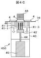
まず、図4A〜図4Dによって、従来の剥離工程について説明する。図4A〜図4Cは、ダイピックアップ装置における従来の突き上げユニットを説明するための略断面図である。また、図4Dは、図4Bの一部を拡大して示した図である。なお、図4A〜図4Cもまた、エキスパンドリングに固定されたウェハの一部分を示している。さらに、図4A〜図4Dでは、紙面上が上方向であり、紙面下が下方向である。 First, a conventional peeling process will be described with reference to FIGS. 4A to 4D. 4A to 4C are schematic cross-sectional views for explaining a conventional push-up unit in the die pickup apparatus. FIG. 4D is an enlarged view of a part of FIG. 4B. 4A to 4C also show a part of the wafer fixed to the expanding ring. Furthermore, in FIGS. 4A to 4D, the upper side is the upper direction and the lower side is the lower direction.
従来の剥離工程は、まず、図4Aに示すような状態からスタートする。即ち、ダイシングテープ16に貼りつけられたウェハ上のピックアップするダイ4の中心に、突き上げユニット450及び吸着ノズル(図4Bの吸着ノズル48を参照)の中心を位置合わせする。この場合、XY(平面)方向に移動するものは、ダイ4、突き上げユニット450、または吸着ノズルの少なくともいずれでも良い。
図4Aの位置合わせ後、突き上げユニット450が上昇し、所定の真空度の真空室43から吸着孔部46に設けられた複数の吸着孔を通して、突き上げユニット450の吸着孔部46の上面部とダイシングテープ16とを密着させる。The conventional peeling process starts from the state shown in FIG. 4A. That is, the centers of the push-up
After the alignment shown in FIG. 4A, the push-up
次に、図4Bに示すように、駆動部45による駆動軸44の上昇に応じて、突き上げブロック本体42が上昇する。突き上げブロック本体42の上昇によって、突き上げブロック本体42上に設けられたニードル41−1〜41−3が、吸着孔部46の吸着孔を通って上昇し、ダイシングテープ16とその上のダイ4を押し上げる。
このとき、ダイ4の上側には吸着ノズル48があり、ダイ4を上方向に吸着する。また、ダイシングテープ16は、吸着孔部46の吸着孔から下方向に吸着される。
この結果、ニードル41−1〜41−3が突き上げている部分から、ダイシングテープ16とダイ4とが剥離していく。Next, as shown in FIG. 4B, the push-up block
At this time, there is a
As a result, the dicing
図4Dは、図4Bの一部(破線円440)を拡大した図である。図4Dに示すように、ダイシングテープ16と接触しているニードル41−3の先端付近(矢印Pが示す)からダイ4が徐々に剥離していく。 FIG. 4D is an enlarged view of a part (broken line circle 440) of FIG. 4B. As shown in FIG. 4D, the
そして、図4Cでは、ダイシングテープ16とダイ4が完全に剥離し、ダイ4は、吸着ノズル48に吸着されて所定のボンディング箇所に移動し、ボンディングがなされる。また、突き上げユニット450の突き上げブロック本体42及びニードル41−1〜41−3は、駆動部45及び駆動軸44によって下降する。 In FIG. 4C, the dicing
上述の図4A〜図4Dのように、従来の剥離工程では、ダイシングテープ16及びダイ4を直接突き上げる突き上げユニットは、金属等の固体であったため、ダイ4を破損する心配があった。
そこで、本発明では、図5A〜図5Cに示すような改良を行った。As described above with reference to FIGS. 4A to 4D, in the conventional peeling process, since the pushing-up unit that directly pushes up the dicing
Therefore, in the present invention, improvements as shown in FIGS. 5A to 5C were performed.
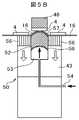
図5A〜図5Cによって、本発明のダイピックアップ方法及びダイボンディング装置の一実施例を説明する。図5A〜図5Cは、ダイピックアップ装置における本発明の突き上げユニットを説明するための略断面図である。また、図5A〜図5Cもまた、エキスパンドリングに固定されたウェハの一部分を示している。さらに、図5A〜図5Cでは、紙面上が上方向であり、紙面下が下方向である。 An embodiment of the die pick-up method and die bonding apparatus of the present invention will be described with reference to FIGS. 5A to 5C. 5A to 5C are schematic cross-sectional views for explaining the push-up unit of the present invention in the die pickup device. 5A-5C also show a portion of the wafer secured to the expanding ring. Further, in FIGS. 5A to 5C, the upper side is the upper direction and the lower side is the lower direction.
本発明の剥離工程は、まず、図5Aに示すような状態からスタートする。即ち、ダイシングテープ16に貼りつけられたピックアップするウェハ上のダイ4の中心に、突き上げユニット50(突き上げ部52)及び吸着ノズル(図5Bの吸着ノズル48を参照)の中心を位置合わせする。この場合、XY(平面)方向に移動するものは、ダイ4、突き上げユニット50、または吸着ノズル48の少なくともいずれでも良い。
図5Aの位置合わせ後、突き上げユニット50を上昇させ、所定の真空度の真空室43から吸着孔部46に設けられた複数の吸着孔を通して、突き上げユニット50の吸着孔部56の上面部とダイシングテープ16とを密着させる。The peeling process of the present invention starts from a state as shown in FIG. 5A. That is, the centers of the push-up unit 50 (push-up portion 52) and the suction nozzle (see the
After the alignment shown in FIG. 5A, the push-up
次に、図5Bに示すように、シリンダ53に図示しないポンプから高圧エアーがパイプ54を介してシリンダ53に供給される。このエアーの流量及び圧力はシリンダ53内の突き上げ部52を上方に突き上げるように供給される。なお、エアーではなく、窒素ガス等、他の気体でも良く、油等の油圧用の液体でも良い。
この結果、突き上げユニット50の突き上げ部52の上部が膨らみ、ダイシングテープ16及びダイ4を上方に突き上げる。
このとき、ダイ4の上側には吸着ノズル48があり、ダイ4を上方向に吸着する。また、ダイシングテープ16は、吸着孔部56の吸着孔から下方向に吸着される。
この結果、突き上げ部52の膨らみから、ダイシングテープ16とダイ4とが剥離していく。Next, as shown in FIG. 5B, high pressure air is supplied to the
As a result, the upper portion of the push-up
At this time, there is a
As a result, the dicing
次に、図5Cに示すように、シリンダ53から図示しないポンプが、パイプ54を介してエアーを減圧する。このように、シリンダ53内のエアーが減圧するため、突き上げ部52は、図5Aの状態に戻るか、さらに下方に引かれて、下方にへこむ。
このように、シリンダ53内のエアーの圧力が減圧され、突き上げ部52の膨らみが無くなり、上側のダイシングテープ16を引き込むことでダイ4とダイシングテープ16とを剥離する(図5C)。
さらに、図5Cにおいて、ダイシングテープ16とダイ4が完全に剥離し、ダイ4は、吸着ノズル48に吸着されて所定のボンディング箇所に移動し、ボンディングがなされる。Next, as shown in FIG. 5C, a pump (not shown) from the
Thus, the pressure of the air in the
Further, in FIG. 5C, the dicing
図5A〜図5Cの実施例の突き上げユニット50は、従来のダイシングテープ16を介してダイ4を突き上げる突き上げ部材(例えば、図4A〜図4Dのニードル41−1〜41−3)が固体であるのに対して、液体等の流体を用いる。即ち、図5A〜図5Cの実施例のダイピックアップ装置における突き上げユニット50では、ダイシングテープ16に接触し、ダイ4を剥離する突き上げ部材(突き上げ部52)は、流体を封じ込めた弾性体である。突き上げ部52は、ダイシングテープ16側とパイプ54側のそれぞれにダイアフラム57と58を配置して、2つのダイアフラム57と58の間に流体を封じ込めてある。また、シリンダ53には、気体が封じ込められている。シリンダ部全体は、下面のダイアフラム58を介して、流体の部屋である上部の突き上げ部52と、気体の部屋である下部のシリンダ53に隔離されている。
また、突き上げ部52を押し上げるシリンダ53は、パイプ54から注入されるエアーの圧力と流量の変化によって動作する。例えば、シリンダ53に高圧エアーが注入されシリンダ53内の圧力が上昇すると、シリンダ53内のピストンとしての突き上げ部52には、上に押し上げようとする力が加えられる。突き上げ部52は、その内部の流体がダイアフラム57と58の間に封じ込まれているため、中央部を頂点として下方から押し上げられ、上方に膨らむ。即ち、シリンダ53の圧力に応じて、下面の膜と上面の膜が上方向に変形する。この、突き上げ部52を構成する上面の膜と下面の膜は、共にダイアフラムであり、圧力の変化に応じて、太鼓や鼓膜のように伸縮するものである。
この突き上げ部52の上面の膜(ダイアフラム57)の上方への膨らみが、ダイシングテープ16を上方に突き上げる。この結果、ダイシングテープ16に貼りつけられたダイ4が、ダイシングテープ16から剥離する。
流体が液体または粉体である場合には、液体または粉体は気体より圧縮性が低いのでバッファーとなり、上面のダイアフラム57を比較的容易にコントロールすることができる。
また、流体が気体の場合には、下面のダイアフラム58を省略することも可能である。この場合には、応答性を良くするため、加える気体の圧力を上げ大気圧より高くする必要がある。この理由は、気体が圧縮性流体であるので、ダイシングテープ16側のダイアフラム57を所定の形状にコントロールすることが難しくなるからである。言い換えると、配管長が長くなると、配管体積と下面のダイアフラムが膨らむ体積比が大きくなるからである。In the push-up
Further, the
The upward bulge of the film (diaphragm 57) on the upper surface of the push-up
When the fluid is a liquid or a powder, the liquid or the powder has a lower compressibility than the gas, so that it becomes a buffer and the
Further, when the fluid is a gas, the
従来の突き上げユニットの場合には、ニードル等、固体による突き上げのため、接触状態によっては、ダイシングテープ及びダイに掛かる圧力分布が不連続になる。そのため、応力集中によってダイの破損(欠け、割れ等)が発生し易かった。
しかし、図5A〜図5Cの実施例によれば、突き上げ時に、液体等の流体によって加圧されるため、ダイ4が貼り付けられたダイシングテープ16との接触部の形状が自由に変形する。この結果、圧力分布が均一に保たれ、ダイ4に無理な力が掛かり難いので、ダイ4の破損が発生し難い。
さらに、従来は、ダイのサイズに合わせて、精密加工した突き上げユニットをそれぞれ設計及び製作する必要があったが、本発明では、流体による接触のため、ダイのサイズに合わせてその都度突き上げユニットを用意する必要がない。また、さらに、ダイのサイズが変わっても、突き上げユニットを交換する必要が少なくなるので、機種変更時の段取り替えの時間を節約することができる。なお、ダイの違いは、シリンダに供給するエアーの流量と圧力を時間的に制御することで対応可能である。In the case of a conventional push-up unit, the pressure distribution applied to the dicing tape and the die becomes discontinuous depending on the contact state due to push-up by a solid such as a needle. For this reason, die damage (chips, cracks, etc.) is likely to occur due to stress concentration.
However, according to the embodiment of FIGS. 5A to 5C, the shape of the contact portion with the dicing
Furthermore, in the past, it was necessary to design and manufacture a precision-worked push-up unit according to the size of the die, but in the present invention, the push-up unit is changed each time according to the size of the die because of contact by fluid. There is no need to prepare. Furthermore, even if the die size changes, the need to replace the push-up unit is reduced, so that the time required for changing the setup when changing the model can be saved. The difference in die can be dealt with by temporally controlling the flow rate and pressure of air supplied to the cylinder.
なお、以上に述べた実施例において、突き上げ部52内の流体は、例えば、水である。また、流体ではなく、粉体であっても良い。
さらに、上述の実施例では、突き上げ部とシリンダはそれぞれ1つで構成した。しかし、複数のシリンダを備え、それぞれに同一若しくは複数の高圧エアーを注入する構成でも良い。またそれぞれのシリンダ内に複数の突き上げ部を有する構成でも良い。In the embodiment described above, the fluid in the push-up
Furthermore, in the above-mentioned embodiment, each of the push-up portion and the cylinder is constituted by one. However, a configuration in which a plurality of cylinders are provided and the same or a plurality of high-pressure air is injected into each of the cylinders may be used. Moreover, the structure which has a some pushing-up part in each cylinder may be sufficient.
1:ウェハ供給部、 2:ワーク供給・搬送部、 3:ダイボンディング部、 4:ダイ(チップ)、 10:ダイボンディング装置、 11:ウェハカセットリフタ、 12:ダイピックアップ装置、 14:ウェハリング、 15:エキスパンドリング、 16:ダイシングテープ、 17:支持リング、 21:スタックローダ、 22:フレームフィーダ、 23:アンローダ、 31:プリフォーム部、 32:ボンディングヘッド部、 41−1、41−2、41−3:ニードル、 42:突き上げブロック本体、 43:真空室、 44:駆動軸、 45:駆動部、 46:吸着孔部、 48:吸着ノズル、 50:突き上げユニット、 52:突き上げ部、 53:シリンダ、54:パイプ、 56:吸着孔部、 57、58:ダイアフラム、 80:制御部、 450:突き上げユニット、 440:破線円。 1: Wafer supply unit, 2: Workpiece supply / conveyance unit, 3: Die bonding unit, 4: Die (chip), 10: Die bonding device, 11: Wafer cassette lifter, 12: Die pickup device, 14: Wafer ring, 15: Expanding ring, 16: Dicing tape, 17: Supporting ring, 21: Stack loader, 22: Frame feeder, 23: Unloader, 31: Preform part, 32: Bonding head part, 41-1, 41-2, 41 -3: needle, 42: push-up block main body, 43: vacuum chamber, 44: drive shaft, 45: drive unit, 46: suction hole, 48: suction nozzle, 50: push-up unit, 52: push-up unit, 53: cylinder 54: Pipe, 56: Adsorption hole, 57, 58: Diaphragm, 80: Control unit, 450: Push-up unit, 440: Dashed circle.
Claims (5)
Translated fromJapanese搬送されてきた前記基板にダイをボンディングするボンディング部と、
前記ダイを有するウェハを供給するウェハ供給部と、
各機器を制御する制御部とから構成されるダイボンディング装置において、
前記ウェハ供給部は、前記ダイをダイシングテープから剥離するためにダイシングテープの下方から突き上げる突き上げユニットを有し、
前記突き上げユニットは、前記ダイシングテープを真空吸着する吸着孔部、流体または粉体を封じ込めた弾性体から成り前記ダイシングテープを突き上げる突き上げ部、前記突き上げ部に圧力をかけるシリンダ、及び、前記制御部の制御により前記シリンダ内の圧力を変更するためのエアーを供給するエアー供給手段を有し、
前記突き上げ部は、前記ダイシングテープ側に配置された第1のダイアフラムと、前記エアー供給手段側に配置された第2のダイアフラムを備え、前記第1のダイアフラムと前記第2のダイアフラムの間に前記流体または粉体が封じ込められており、
前記シリンダは、前記第2のダイアフラムにより、前記流体または粉体の部屋である上部の突き上げ部と、前記エアーの部屋である下部のシリンダに隔離されていることを特徴とするダイボンディング装置。A workpiece supply / transport section for transporting substrates,
A bonding part for bonding a die to the substrate that has been transported;
A wafer supply unit for supplying a wafer having the die;
In a die bonding apparatus composed of a control unit that controls each device,
The wafer supply unit has a push-up unit that pushes up from below the dicing tape in order to peel the die from the dicing tape,
The push-up unit includes a suction hole portion that vacuum-sucks the dicing tape, a push-up portion that pushes up the dicing tape, and a cylinder that applies pressure to the push-up portion. controlled byhave a air supply means for supplying air to change the pressure in thecylinder,
The push-up portion includes a first diaphragm disposed on the dicing tape side and a second diaphragm disposed on the air supply unit side, and the first diaphragm and the second diaphragm are disposed between the first diaphragm and the second diaphragm. Fluid or powder is contained,
The die bonding apparatus accordingto claim 1, wherein the cylinder is separated by an upper push-up portion that is the fluid or powder chamber and a lower cylinder that is the air chamber by the second diaphragm .
前記突き上げ部は、前記ダイシングテープ側に配置された第1のダイアフラムと、前記エアー供給手段側に配置された第2のダイアフラムを備え、前記第1のダイアフラムと前記第2のダイアフラムの間に前記流体または粉体が封じ込められており、
前記シリンダは、前記第2のダイアフラムにより、前記流体または粉体の部屋である上部の突き上げ部と、前記エアーの部屋である下部のシリンダに隔離されていることを特徴とするダイピックアップ装置。The dicing tape comprising a vacuum chamber having a predetermined degree of vacuum, a suction hole portion having a plurality of suction holes connected to the vacuum chamber for vacuum suction of the dicing tape, and an elastic body containing fluid or powder.possess a push-up portion pushes up from the bottom, a cylinder applying pressure to the push-up unit, and air supply means for supplying air to change the pressure in thecylinder,
The push-up portion includes a first diaphragm disposed on the dicing tape side and a second diaphragm disposed on the air supply unit side, and the first diaphragm and the second diaphragm are disposed between the first diaphragm and the second diaphragm. Fluid or powder is contained,
The die pick-up apparatus, wherein the cylinder is separated by an upper push-up portion that is the fluid or powder chamber and a lower cylinder that is the air chamber by the second diaphragm .
前記突き上げ部は、前記ダイシングテープ側に配置された第1のダイアフラムと、前記エアー供給手段側に配置された第2のダイアフラムを備え、前記第1のダイアフラムと前記第2のダイアフラムの間に前記流体または粉体が封じ込められており、
前記シリンダは、前記第2のダイアフラムにより、前記流体または粉体の部屋である上部の突き上げ部と、前記エアーの部屋である下部のシリンダに隔離されており、
前記ダイシングテープに貼りつけられたピックアップするウェハ上のダイの中心に、前記突き上げ部及び吸着ノズルの中心を位置合わせし、
前記突き上げユニットを上昇させ、前記複数の吸着孔を通して、前記吸着孔部の上面部と前記ダイシングテープとを密着させ、
前記シリンダ内のエアーの圧力を上げることによって、前記シリンダ内の前記突き上げ部の上面を上方に突き上げて、前記ダイシングテープ及び前記ダイを上方に突き上げ、
前記シリンダ内のエアーの圧力を下げて前記突き上げ部の上面をへこませ、
前記ダイと前記ダイシングテープとを剥離することを特徴とするダイピックアップ方法。The dicing tape comprising a vacuum chamber having a predetermined degree of vacuum, a suction hole portion having a plurality of suction holes connected to the vacuum chamber for vacuum suction of the dicing tape, and an elastic body containing fluid or powder. A push-up unit that pushes up from below, a cylinder that applies pressure to the push-up part, and an air supply unit that supplies air for changing the pressure in the cylinder,
The push-up portion includes a first diaphragm disposed on the dicing tape side and a second diaphragm disposed on the air supply unit side, and the first diaphragm and the second diaphragm are disposed between the first diaphragm and the second diaphragm. Fluid or powder is contained,
The cylinder is separated by the second diaphragm into an upper push-up portion that is the fluid or powder chamber and a lower cylinder that is the air chamber,
The center of the push-up portion and the suction nozzle is aligned with the center of the die on the wafer to be picked up attached to the dicing tape,
Raise the push-up unit, and through the plurality of suction holes, closely contact the upper surface portion of the suction hole portion and the dicing tape,
By raising the pressure of the air in the cylinder, the upper surface of the push-up portion in the cylinder is pushed up, the dicing tape and the die are pushed up,
Reducing the air pressure in the cylinder and denting the upper surface of the push-up part,
A die pickup method, wherein the die and the dicing tape are peeled off.
Priority Applications (5)
| Application Number | Priority Date | Filing Date | Title |
|---|---|---|---|
| JP2012188339AJP6055239B2 (en) | 2012-08-29 | 2012-08-29 | DIE BONDING DEVICE, DIE PICKUP DEVICE, AND DIE PICKUP METHOD |
| TW102106525ATWI524407B (en) | 2012-08-29 | 2013-02-25 | A grain bonding apparatus, a grain picking apparatus, and a grain picking method |
| KR1020130019819AKR101449834B1 (en) | 2012-08-29 | 2013-02-25 | Die bonding apparatus, die pickup apparatus and die pickup method |
| CN201310061127.XACN103681406B (en) | 2012-08-29 | 2013-02-27 | Nude film engagement device, bare chip pickup device and nude film pick-up method |
| US13/779,934US9245778B2 (en) | 2012-08-29 | 2013-02-28 | Die bonding apparatus, die picking up apparatus and die picking up method |
Applications Claiming Priority (1)
| Application Number | Priority Date | Filing Date | Title |
|---|---|---|---|
| JP2012188339AJP6055239B2 (en) | 2012-08-29 | 2012-08-29 | DIE BONDING DEVICE, DIE PICKUP DEVICE, AND DIE PICKUP METHOD |
Publications (2)
| Publication Number | Publication Date |
|---|---|
| JP2014049452A JP2014049452A (en) | 2014-03-17 |
| JP6055239B2true JP6055239B2 (en) | 2016-12-27 |
Family
ID=50185791
Family Applications (1)
| Application Number | Title | Priority Date | Filing Date |
|---|---|---|---|
| JP2012188339AActiveJP6055239B2 (en) | 2012-08-29 | 2012-08-29 | DIE BONDING DEVICE, DIE PICKUP DEVICE, AND DIE PICKUP METHOD |
Country Status (5)
| Country | Link |
|---|---|
| US (1) | US9245778B2 (en) |
| JP (1) | JP6055239B2 (en) |
| KR (1) | KR101449834B1 (en) |
| CN (1) | CN103681406B (en) |
| TW (1) | TWI524407B (en) |
Families Citing this family (33)
| Publication number | Priority date | Publication date | Assignee | Title |
|---|---|---|---|---|
| EP2296168A1 (en)* | 2009-09-09 | 2011-03-16 | Kulicke & Soffa Die Bonding GmbH | Tool for picking a planar object from a supply station |
| KR101596461B1 (en)* | 2014-04-01 | 2016-02-23 | 주식회사 프로텍 | Apparatus and Method for Chip Detaching |
| DE102015100512A1 (en)* | 2015-01-14 | 2016-07-14 | Infineon Technologies Austria Ag | Embrittlement device, recording system and method for picking up chips |
| TWI566317B (en)* | 2015-03-13 | 2017-01-11 | 均華精密工業股份有限公司 | Apparatus for wafer ring rapid reloading and method using the same |
| KR101683398B1 (en)* | 2015-10-02 | 2016-12-07 | 주식회사 프로텍 | Apparatus and Method for Chip Detaching |
| CN107221510B (en)* | 2016-03-22 | 2020-09-15 | 晟碟信息科技(上海)有限公司 | System and method for separating semiconductor die from die attach film tape |
| JP6705727B2 (en)* | 2016-09-26 | 2020-06-03 | ファスフォードテクノロジ株式会社 | Flip chip bonder and method for manufacturing semiconductor device |
| WO2018086698A1 (en)* | 2016-11-10 | 2018-05-17 | Applied Materials, Inc. | Holding arrangement for holding a substrate, carrier including the holding arrangement, processing system employing the carrier, and method for releasing a substrate from a holding arrangement |
| JP6621771B2 (en)* | 2017-01-25 | 2019-12-18 | ファスフォードテクノロジ株式会社 | Semiconductor manufacturing apparatus and semiconductor device manufacturing method |
| JP6653273B2 (en)* | 2017-01-26 | 2020-02-26 | ファスフォードテクノロジ株式会社 | Semiconductor manufacturing apparatus and semiconductor device manufacturing method |
| KR101970193B1 (en)* | 2017-04-25 | 2019-08-13 | 스테코 주식회사 | Apparatus for separating chip from mounting tape and method thereof |
| WO2019008674A1 (en)* | 2017-07-04 | 2019-01-10 | 株式会社Fuji | Component mounting device |
| US10700038B2 (en)* | 2017-08-25 | 2020-06-30 | Micron Technology, Inc. | Methods and systems for inhibiting bonding materials from contaminating a semiconductor processing tool |
| JP7102113B2 (en)* | 2017-09-11 | 2022-07-19 | ファスフォードテクノロジ株式会社 | Manufacturing method of die bonding equipment and semiconductor equipment |
| JP2019169516A (en)* | 2018-03-22 | 2019-10-03 | 東芝メモリ株式会社 | Thrusting-up device and thrusting-up method for semiconductor device |
| KR102037967B1 (en)* | 2018-05-30 | 2019-10-29 | 세메스 주식회사 | Die bonding method |
| JP2019212818A (en)* | 2018-06-06 | 2019-12-12 | 株式会社ディスコ | Wafer processing method |
| JP2019212816A (en)* | 2018-06-06 | 2019-12-12 | 株式会社ディスコ | Wafer processing method |
| JP2019212817A (en)* | 2018-06-06 | 2019-12-12 | 株式会社ディスコ | Wafer processing method |
| KR102617347B1 (en)* | 2018-10-04 | 2023-12-26 | 삼성전자주식회사 | Die ejector and die supplying apparatus including the same |
| KR102594542B1 (en)* | 2018-10-31 | 2023-10-26 | 세메스 주식회사 | Die ejecting apparatus |
| TWI734434B (en)* | 2019-04-11 | 2021-07-21 | 日商新川股份有限公司 | Joining device |
| KR102221703B1 (en)* | 2019-04-19 | 2021-03-02 | 세메스 주식회사 | Die ejector and apparatus for picking up dies including the same |
| JP7326861B2 (en)* | 2019-05-17 | 2023-08-16 | 三菱電機株式会社 | Semiconductor manufacturing equipment and semiconductor device manufacturing method |
| KR20210009843A (en)* | 2019-07-18 | 2021-01-27 | 세메스 주식회사 | Die pickup method |
| KR102365660B1 (en)* | 2019-08-27 | 2022-02-18 | 세메스 주식회사 | Die pickup module and die bonding apparatus including the same |
| CN110504208B (en)* | 2019-09-24 | 2021-11-16 | 大连佳峰自动化股份有限公司 | Thimble system |
| KR102635493B1 (en)* | 2020-11-04 | 2024-02-07 | 세메스 주식회사 | Apparatus for transferring die in bonding equipment and method thereof |
| US20220165590A1 (en)* | 2020-11-23 | 2022-05-26 | Sj Semiconductor(Jiangyin) Corporation | Die pickup device and method |
| US11764098B2 (en)* | 2021-04-16 | 2023-09-19 | Asmpt Singapore Pte. Ltd. | Detaching a die from an adhesive tape by air ejection |
| JP7660459B2 (en)* | 2021-08-05 | 2025-04-11 | 東京エレクトロン株式会社 | Bonding device and bonding method |
| JP2023074768A (en)* | 2021-11-18 | 2023-05-30 | 株式会社ディスコ | Tape crimping device |
| TWI834450B (en)* | 2022-12-26 | 2024-03-01 | 梭特科技股份有限公司 | Method for stripping die with pushing means and air control means |
Family Cites Families (12)
| Publication number | Priority date | Publication date | Assignee | Title |
|---|---|---|---|---|
| JP2839215B2 (en)* | 1991-09-04 | 1998-12-16 | 株式会社カイジョー | Bonding equipment |
| JPH0745558A (en)* | 1993-08-02 | 1995-02-14 | Fujitsu Ltd | Method of peeling semiconductor chip |
| KR100278603B1 (en)* | 1998-09-30 | 2001-01-15 | 윤종용 | Die bonding equipment and die bonding method for microgap ball grid array packages |
| JP3610941B2 (en)* | 2001-10-05 | 2005-01-19 | 松下電器産業株式会社 | Electronic component mounting equipment |
| JP4206320B2 (en)* | 2003-09-19 | 2009-01-07 | 株式会社ルネサステクノロジ | Manufacturing method of semiconductor integrated circuit device |
| US7005317B2 (en)* | 2003-10-27 | 2006-02-28 | Intel Corporation | Controlled fracture substrate singulation |
| JP2007103826A (en)* | 2005-10-07 | 2007-04-19 | Matsushita Electric Ind Co Ltd | Semiconductor chip pickup device |
| JP4765536B2 (en)* | 2005-10-14 | 2011-09-07 | パナソニック株式会社 | Chip pickup apparatus, chip pickup method, chip peeling apparatus and chip peeling method |
| JP4924316B2 (en)* | 2007-09-14 | 2012-04-25 | 日本電気株式会社 | Semiconductor manufacturing apparatus and semiconductor manufacturing method |
| JP4985513B2 (en)* | 2008-03-26 | 2012-07-25 | 富士通セミコンダクター株式会社 | Method and apparatus for peeling electronic parts |
| WO2011122635A1 (en)* | 2010-03-30 | 2011-10-06 | 住友化学株式会社 | Method for manufacturing a honeycomb-structured object |
| JP5123357B2 (en)* | 2010-06-17 | 2013-01-23 | 株式会社日立ハイテクインスツルメンツ | Die bonder and pickup device |
- 2012
- 2012-08-29JPJP2012188339Apatent/JP6055239B2/enactiveActive
- 2013
- 2013-02-25KRKR1020130019819Apatent/KR101449834B1/enactiveActive
- 2013-02-25TWTW102106525Apatent/TWI524407B/enactive
- 2013-02-27CNCN201310061127.XApatent/CN103681406B/enactiveActive
- 2013-02-28USUS13/779,934patent/US9245778B2/enactiveActive
Also Published As
| Publication number | Publication date |
|---|---|
| TWI524407B (en) | 2016-03-01 |
| CN103681406B (en) | 2016-07-06 |
| KR20140029115A (en) | 2014-03-10 |
| CN103681406A (en) | 2014-03-26 |
| TW201409554A (en) | 2014-03-01 |
| KR101449834B1 (en) | 2014-10-08 |
| JP2014049452A (en) | 2014-03-17 |
| US20140060751A1 (en) | 2014-03-06 |
| US9245778B2 (en) | 2016-01-26 |
Similar Documents
| Publication | Publication Date | Title |
|---|---|---|
| JP6055239B2 (en) | DIE BONDING DEVICE, DIE PICKUP DEVICE, AND DIE PICKUP METHOD | |
| JP5805411B2 (en) | Die bonder pickup method and die bonder | |
| KR101970884B1 (en) | Apparatus for manufacturing semiconductor and method of manufacturing semiconductor device | |
| JP5123357B2 (en) | Die bonder and pickup device | |
| KR100506109B1 (en) | Separation mechanism for adhesive tape, separation apparatus for adhesive tape, separation method for adhesive tape, pickup apparatus for semiconductor chip, pickup method for semiconductor chip, manufacturing method for semiconductor apparatus, and manufacturing apparatus for semiconductor apparatus | |
| JP4864816B2 (en) | Manufacturing method of semiconductor integrated circuit device | |
| KR102066874B1 (en) | Semiconductor manufacturing device and manufacturing method of semiconductor device | |
| JP6941513B2 (en) | Semiconductor manufacturing equipment and manufacturing method of semiconductor equipment | |
| JP2015076410A (en) | Bonding method and die bonder | |
| KR102490394B1 (en) | Die bonding apparatus, manufacturing method of semiconductor apparatus and peeling apparatus | |
| JPWO2005029574A1 (en) | Collet, die bonder and chip pickup method | |
| US20140238618A1 (en) | Die ejector and die separation method | |
| US20220238357A1 (en) | Die Bonding Apparatus and Manufacturing Method for Semiconductor Device | |
| JP2018120938A (en) | Semiconductor manufacturing apparatus and method for manufacturing semiconductor device | |
| JP2005191535A (en) | Pasting apparatus and pasting method | |
| JP6211359B2 (en) | Flip chip bonder and bonding method | |
| JP2013034001A (en) | Die bonder, pickup method, and pickup device | |
| JP2009253060A (en) | Manufacturing method of semiconductor integrated circuit device | |
| JP2014239090A (en) | Pickup system | |
| JP5214739B2 (en) | Chip peeling method, semiconductor device manufacturing method, and chip peeling apparatus | |
| KR101115932B1 (en) | Semiconductor die attach device | |
| JP2008244125A (en) | Electronic component mounting tool, mounting apparatus, and mounting method | |
| JP2017041532A (en) | Chip peeling device and chip peeling method | |
| JP2012039153A (en) | Manufacturing method of semiconductor integrated circuit device | |
| JP2013219403A (en) | Manufacturing method of semiconductor integrated circuit device |
Legal Events
| Date | Code | Title | Description |
|---|---|---|---|
| A711 | Notification of change in applicant | Free format text:JAPANESE INTERMEDIATE CODE: A712 Effective date:20150330 | |
| RD02 | Notification of acceptance of power of attorney | Free format text:JAPANESE INTERMEDIATE CODE: A7422 Effective date:20150508 | |
| A621 | Written request for application examination | Free format text:JAPANESE INTERMEDIATE CODE: A621 Effective date:20150812 | |
| A977 | Report on retrieval | Free format text:JAPANESE INTERMEDIATE CODE: A971007 Effective date:20160623 | |
| A131 | Notification of reasons for refusal | Free format text:JAPANESE INTERMEDIATE CODE: A131 Effective date:20160628 | |
| A521 | Request for written amendment filed | Free format text:JAPANESE INTERMEDIATE CODE: A523 Effective date:20160721 | |
| A521 | Request for written amendment filed | Free format text:JAPANESE INTERMEDIATE CODE: A523 Effective date:20160823 | |
| TRDD | Decision of grant or rejection written | ||
| A01 | Written decision to grant a patent or to grant a registration (utility model) | Free format text:JAPANESE INTERMEDIATE CODE: A01 Effective date:20161115 | |
| A61 | First payment of annual fees (during grant procedure) | Free format text:JAPANESE INTERMEDIATE CODE: A61 Effective date:20161202 | |
| R150 | Certificate of patent or registration of utility model | Ref document number:6055239 Country of ref document:JP Free format text:JAPANESE INTERMEDIATE CODE: R150 | |
| R250 | Receipt of annual fees | Free format text:JAPANESE INTERMEDIATE CODE: R250 | |
| R250 | Receipt of annual fees | Free format text:JAPANESE INTERMEDIATE CODE: R250 | |
| R250 | Receipt of annual fees | Free format text:JAPANESE INTERMEDIATE CODE: R250 | |
| R250 | Receipt of annual fees | Free format text:JAPANESE INTERMEDIATE CODE: R250 | |
| R250 | Receipt of annual fees | Free format text:JAPANESE INTERMEDIATE CODE: R250 | |
| R250 | Receipt of annual fees | Free format text:JAPANESE INTERMEDIATE CODE: R250 |