JP6055225B2 - Display device with touch panel - Google Patents
Display device with touch panelDownload PDFInfo
- Publication number
- JP6055225B2 JP6055225B2JP2012168371AJP2012168371AJP6055225B2JP 6055225 B2JP6055225 B2JP 6055225B2JP 2012168371 AJP2012168371 AJP 2012168371AJP 2012168371 AJP2012168371 AJP 2012168371AJP 6055225 B2JP6055225 B2JP 6055225B2
- Authority
- JP
- Japan
- Prior art keywords
- terminals
- flexible substrate
- touch panel
- display device
- substrate
- Prior art date
- Legal status (The legal status is an assumption and is not a legal conclusion. Google has not performed a legal analysis and makes no representation as to the accuracy of the status listed.)
- Active
Links
Images


Classifications
- G—PHYSICS
- G06—COMPUTING OR CALCULATING; COUNTING
- G06F—ELECTRIC DIGITAL DATA PROCESSING
- G06F3/00—Input arrangements for transferring data to be processed into a form capable of being handled by the computer; Output arrangements for transferring data from processing unit to output unit, e.g. interface arrangements
- G06F3/01—Input arrangements or combined input and output arrangements for interaction between user and computer
- G06F3/03—Arrangements for converting the position or the displacement of a member into a coded form
- G06F3/041—Digitisers, e.g. for touch screens or touch pads, characterised by the transducing means
- G06F3/0412—Digitisers structurally integrated in a display
- G—PHYSICS
- G02—OPTICS
- G02F—OPTICAL DEVICES OR ARRANGEMENTS FOR THE CONTROL OF LIGHT BY MODIFICATION OF THE OPTICAL PROPERTIES OF THE MEDIA OF THE ELEMENTS INVOLVED THEREIN; NON-LINEAR OPTICS; FREQUENCY-CHANGING OF LIGHT; OPTICAL LOGIC ELEMENTS; OPTICAL ANALOGUE/DIGITAL CONVERTERS
- G02F1/00—Devices or arrangements for the control of the intensity, colour, phase, polarisation or direction of light arriving from an independent light source, e.g. switching, gating or modulating; Non-linear optics
- G02F1/01—Devices or arrangements for the control of the intensity, colour, phase, polarisation or direction of light arriving from an independent light source, e.g. switching, gating or modulating; Non-linear optics for the control of the intensity, phase, polarisation or colour
- G02F1/13—Devices or arrangements for the control of the intensity, colour, phase, polarisation or direction of light arriving from an independent light source, e.g. switching, gating or modulating; Non-linear optics for the control of the intensity, phase, polarisation or colour based on liquid crystals, e.g. single liquid crystal display cells
- G02F1/133—Constructional arrangements; Operation of liquid crystal cells; Circuit arrangements
- G02F1/1333—Constructional arrangements; Manufacturing methods
- G02F1/13338—Input devices, e.g. touch panels
- G—PHYSICS
- G06—COMPUTING OR CALCULATING; COUNTING
- G06F—ELECTRIC DIGITAL DATA PROCESSING
- G06F3/00—Input arrangements for transferring data to be processed into a form capable of being handled by the computer; Output arrangements for transferring data from processing unit to output unit, e.g. interface arrangements
- G06F3/01—Input arrangements or combined input and output arrangements for interaction between user and computer
- G06F3/03—Arrangements for converting the position or the displacement of a member into a coded form
- G06F3/041—Digitisers, e.g. for touch screens or touch pads, characterised by the transducing means
- G06F3/044—Digitisers, e.g. for touch screens or touch pads, characterised by the transducing means by capacitive means
Landscapes
- Engineering & Computer Science (AREA)
- Physics & Mathematics (AREA)
- General Engineering & Computer Science (AREA)
- Theoretical Computer Science (AREA)
- General Physics & Mathematics (AREA)
- Human Computer Interaction (AREA)
- Nonlinear Science (AREA)
- Liquid Crystal (AREA)
- Chemical & Material Sciences (AREA)
- Crystallography & Structural Chemistry (AREA)
- Mathematical Physics (AREA)
- Optics & Photonics (AREA)
- Devices For Indicating Variable Information By Combining Individual Elements (AREA)
- Position Input By Displaying (AREA)
Description
Translated fromJapanese本発明は、タッチパネル付表示装置に関する。 The present invention relates to a display device with a touch panel.
近年、コンピュータ等の情報通信端末において、表示装置の上にタッチパネルを重ねて配置し、タッチパネル入力機能付の表示装置としたものが広く用いられている。このうち表示機能を担う装置として一般的に普及している液晶表示装置は、薄膜トランジスタ基板(以下、「TFT(Thin Film Transistor)基板」という。)とカラーフィルタ基板の2つの基板の間に封じ込められた液晶組成物の配向を電界の変化により変え、光の透過度合いを制御することにより画像を表示させる装置である。このような液晶表示装置において、TFT基板側に画素電極と共通電極の両方を配置することにより、いわゆる横電界を形成し、視野角の大きい表示を実現したIPS(In Plane Switching)方式が広く用いられている。 In recent years, in information communication terminals such as computers, a display device having a touch panel input function in which a touch panel is placed on a display device is widely used. Among these, a liquid crystal display device that is generally spread as a device having a display function is enclosed between a thin film transistor substrate (hereinafter referred to as a “TFT (Thin Film Transistor) substrate”) and a color filter substrate. This is a device that displays an image by changing the orientation of the liquid crystal composition by changing the electric field and controlling the degree of light transmission. In such a liquid crystal display device, an IPS (In Plane Switching) system is widely used, in which both a pixel electrode and a common electrode are arranged on the TFT substrate side, thereby forming a so-called lateral electric field and realizing a display with a large viewing angle. It has been.
タッチパネルは、使用者の指などを用いてタッチされたパネル上の座標を認識し、処理装置にその座標に基づいた処理を行なわせる入力装置である。パッチパネルには、タッチされた部分の抵抗値変化を検出する抵抗膜方式、タッチにより遮蔽された部分の光量変化を検出する光センサ方式、容量変化を検出する静電容量結合方式などが知られている。静電容量結合方式は、パネルの透過率が高く表示画質を低下させない点、他の電極との接触がなく耐久性が高い点等から広く用いられている。 The touch panel is an input device that recognizes coordinates on a touched panel using a user's finger or the like and causes the processing device to perform processing based on the coordinates. For the patch panel, a resistance film method for detecting a change in resistance value of a touched portion, an optical sensor method for detecting a light amount change in a portion shielded by touch, a capacitance coupling method for detecting a capacitance change, and the like are known. ing. The capacitive coupling method is widely used because it has a high panel transmittance and does not deteriorate the display image quality, has no contact with other electrodes, and has high durability.
近年、情報通信端末に対する小型化・薄型化の要請により、タッチパネル付液晶表示装置もより薄型のものが求められている。特許文献1には、IPS方式の液晶表示装置において、液晶表示装置の共通電極をタッチパネルの駆動電極として用いることにより、より薄型化されたタッチパネル付液晶表示装置が開示されている。 2. Description of the Related Art In recent years, a liquid crystal display device with a touch panel is required to be thinner due to a demand for downsizing and thinning information communication terminals. Patent Document 1 discloses a liquid crystal display device with a touch panel that is made thinner by using a common electrode of the liquid crystal display device as a drive electrode of the touch panel in an IPS liquid crystal display device.
TFT基板のガラス基板上の配線から信号を取り出すには、FPC(Flexible Printed Circuits)等のフレキシブルケーブルをACF(Anisotropic Conductive Film)等の導電性の接着性材料を用いて接続するのが一般的である。この場合、FPCが接続される部分のTFT基板は透明であり、FPCが接続されるTFT基板面の反対側から視認可能であるため、予め薄膜形成工程の段階でTFT基板にアライメントマークを作成しておくことにより、アライメントマークに視認しながら高い精度でFPCを接続することが可能である。 In order to extract signals from the wiring on the glass substrate of the TFT substrate, it is common to connect a flexible cable such as FPC (Flexible Printed Circuits) using a conductive adhesive material such as ACF (Anisotropic Conductive Film). is there. In this case, the TFT substrate of the portion to which the FPC is connected is transparent and visible from the opposite side of the TFT substrate surface to which the FPC is connected. Therefore, an alignment mark is previously created on the TFT substrate at the thin film formation step. Thus, it is possible to connect the FPC with high accuracy while visually recognizing the alignment mark.
一方、上述の特許文献1に記載されたようなタッチパネル付液晶表示装置では、タッチ検出のための検出電極がカラーフィルタ基板上に配置されているため、カラーフィルタ基板上から信号を取り出す必要がある。しかしながら、カラーフィルタ基板の周囲には遮光膜が形成されており透明でないため、TFT基板と同様のアライメントマークを利用した位置合わせは難しい。 On the other hand, in the liquid crystal display device with a touch panel as described in Patent Document 1 described above, since the detection electrode for touch detection is arranged on the color filter substrate, it is necessary to take out a signal from the color filter substrate. . However, since a light shielding film is formed around the color filter substrate and is not transparent, alignment using alignment marks similar to those of the TFT substrate is difficult.
本発明は、上述の事情を鑑みてしたものであり、カラーフィルタ基板上から電気信号を取り出すことのできるタッチパネル付表示装置を提供することを目的とする。 The present invention has been made in view of the above-described circumstances, and an object of the present invention is to provide a display device with a touch panel that can extract an electrical signal from a color filter substrate.
本発明のタッチパネル付表示装置は、表示領域に形成された各画素に対応して薄膜トランジスタが形成された薄膜トランジスタ基板と、前記薄膜トランジスタ基板と対向して配置された対向基板と、を備え、前記対向基板は、背面に表示領域を囲んで遮光膜を備え、前記遮光膜によって前記表示領域を囲む遮光領域を形成し、前記対向基板は、前面に前記表示領域を横切って一方向に延びて前記表示領域上に外部からの接触があった場合に接触位置を検出する複数の検出電極と、前記検出電極に接続している複数の電極端子とを備え、前記対向基板には前記検出電極からの信号を取り出すためのフレキシブル基板が接続され、前記フレキシブル基板は、複数のフレキシブル基板端子を有し、前記電極端子と前記フレキシブル基板端子とが前記遮光領域で接続され、前記複数のフレキシブル基板端子の配置の周期と、前記複数の電極端子の配置の周期とは異なっている、ことを特徴とするタッチパネル付表示装置である。 A display device with a touch panel according to the present invention includes a thin film transistor substrate in which a thin film transistor is formed corresponding to each pixel formed in a display region, and a counter substrate disposed to face the thin film transistor substrate, and the counter substrate Includes a light-shielding film surrounding the display area on the back surface, and forming the light-shielding area surrounding the display area by the light-shielding film, and the counter substrate extends in one direction across the display area on the front surface and the display area A plurality of detection electrodes for detecting a contact position when there is an external contact on the top, and a plurality of electrode terminals connected to the detection electrode, and a signal from the detection electrode is sent to the counter substrate A flexible substrate for taking out is connected, the flexible substrate has a plurality of flexible substrate terminals, and the electrode terminal and the flexible substrate terminal are Are connected in the optical domain, the period of arrangement of said plurality of flexible substrate terminal, said different from the period of the arrangement of a plurality of electrode terminals, it is a display device with a touch panel according to claim.
また、本発明のタッチパネル付表示装置において、前記対向基板は、前記各画素ごとに所定の波長領域の光を通過させるカラーフィルタであり、前記検出電極及び前記電極端子は透明導電膜で形成されていることとしてもよい。 In the display device with a touch panel according to the present invention, the counter substrate is a color filter that transmits light in a predetermined wavelength region for each pixel, and the detection electrode and the electrode terminal are formed of a transparent conductive film. It is good to be.
また、本発明のタッチパネル付表示装置において、前記複数の電極端子の各々は、2以上の前記フレキシブル基板端子と電気的に接続され、前記複数のフレキシブル基板端子の一部は、前記フレキシブル基板内で電気的にフローティングであるダミー端子であってもよい。 In the display device with a touch panel according to the present invention, each of the plurality of electrode terminals is electrically connected to two or more of the flexible substrate terminals, and some of the plurality of flexible substrate terminals are within the flexible substrate. It may be a dummy terminal that is electrically floating.
また、本発明のタッチパネル付表示装置において、前記ダミー端子は、前記複数の電極端子の配置の周期で形成されていてもよい。 In the display device with a touch panel according to the present invention, the dummy terminals may be formed with a period of arrangement of the plurality of electrode terminals.
また、本発明のタッチパネル付表示装置において、前記ダミー端子は2以上連続して配置されていてもよい。 In the display device with a touch panel according to the present invention, two or more dummy terminals may be continuously arranged.
以下、本発明の実施形態について、図面を参照しつつ説明する。なお、図面において、同一又は同等の要素には同一の符号を付し、重複する説明を省略する。 Embodiments of the present invention will be described below with reference to the drawings. In the drawings, the same or equivalent elements are denoted by the same reference numerals, and redundant description is omitted.
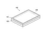
図1は、本発明の一実施形態に係るタッチパネル付表示装置100について示す図である。この図に示されるように、タッチパネル付表示装置100は、タッチパネル付表示パネル200と、タッチパネル付表示パネル200を挟むように固定する上フレーム101及び下フレーム102と、により構成されている。 FIG. 1 is a diagram illustrating a
図2は、タッチパネル付表示パネル200について概略的に示す図である。本発明の一実施形態に係るタッチパネル付液晶表示装置は、表示領域に形成された各画素に対応して薄膜トランジスタが形成された薄膜トランジスタ基板と、薄膜トランジスタ基板と対向して配置された対向基板とを備える。 FIG. 2 is a diagram schematically illustrating the
対向基板は、背面に表示領域を囲んで遮光膜を備え、遮光膜によって表示領域を囲む遮光領域を形成している。また、対向基板は、前面に表示領域を横切って一方向に延びて表示領域上に外部からの接触があった場合に接触位置を検出する複数の検出電極と、検出電極に接続している複数の電極端子とを備える。さらに、対向基板には検出電極からの信号を取り出すためのフレキシブル基板が接続される。 The counter substrate includes a light shielding film surrounding the display area on the back surface, and a light shielding area surrounding the display area is formed by the light shielding film. The counter substrate extends in one direction across the display area on the front surface and has a plurality of detection electrodes for detecting a contact position when there is external contact on the display area, and a plurality connected to the detection electrodes. Electrode terminals. Further, a flexible substrate for extracting a signal from the detection electrode is connected to the counter substrate.
フレキシブル基板は、電極端子と接続するための複数のフレキシブル基板端子をそなえる。電極端子とフレキシブル基板端子とは遮光領域内で接続している。複数のフレキシブル基板端子の配置の周期と、複数の電極端子の配置の周期とは異なって形成されている。 The flexible substrate includes a plurality of flexible substrate terminals for connection to the electrode terminals. The electrode terminal and the flexible substrate terminal are connected within the light shielding region. The period of arrangement of the plurality of flexible substrate terminals is different from the period of arrangement of the plurality of electrode terminals.
以下、タッチパネル付表示パネルとして、タッチパネル付き液晶表示パネルを一例にして説明する。タッチパネル付液晶表示装置の場合、対向基板はカラーフィルタ基板であり、遮光膜はブラックマトリクスである。 Hereinafter, as a display panel with a touch panel, a liquid crystal display panel with a touch panel will be described as an example. In the case of a liquid crystal display device with a touch panel, the counter substrate is a color filter substrate, and the light shielding film is a black matrix.
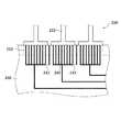
タッチパネル付液晶表示パネル200は、TFT基板210と、TFT基板210との間に液晶組成物を封止して重ね合わされたカラーフィルタ基板220と、を備えており、TFT基板210には、TFT基板の各画素のトランジスタを駆動させるためのドライバIC(Integrated Circuit)212が配置され、更にドライバIC212に外部から信号を入力させるためのTFTフレキシブル基板215が取り付けられている。 The liquid
一方、カラーフィルタ基板220は、光漏れを防ぐために、R(赤)G(緑)B(青)のカラーフィルタを有する各画素が配置された表示領域の周囲に形成された遮光膜229と、表示領域内で一方向に延びる複数の並置された電極であり、画面への接触を検知するタッチパネル検出電極222と、タッチパネル検出電極222から一体的に接続され表示領域の外に形成された透明電極端子223と、カラーフィルタ基板220の表示領域を覆うように配置された上偏光板250と、を有している。画像表示領域を囲んで遮光膜229を形成した領域が遮光領域である。また、更に、カラーフィルタ基板220には、カラーフィルタ基板220の透明電極端子223とTFTフレキシブル基板215の端子216とを接続し、カラーフィルタ基板220からタッチを検出する信号を伝えるCF(Color Filter)フレキシブル基板240が接続されている。透明電極端子223とフレキシブル基板215の端子216は遮光領域で接続されている。 On the other hand, in order to prevent light leakage, the
図3には、図2のIII−III線における断面が概略的に示されている。ここで、TFT基板210及びTFTフレキシブル基板215、並びにカラーフィルタ基板220及びCFフレキシブル基板240とは、不図示のACF(Anisotropic Conductive Film)により接着されている。この図に示されるように、CFフレキシブル基板240がカラーフィルタ基板220上に接続された位置は、遮光膜229と重なる位置となっている。 FIG. 3 schematically shows a cross section taken along line III-III in FIG. Here, the
図4は、CFフレキシブル基板240とカラーフィルタ基板220との接続部分について拡大して詳細に示す図である。この図に示されるように、カラーフィルタ基板220にタッチパネル検出電極222と連続的に形成された透明電極端子223は、カラーフィルタ基板220の端部にまで延びている。また、CFフレキシブル基板240は、透明電極端子223の配置の周期とは異なる配置の周期で形成されたフレキシブル基板端子242及び243を有し、特に本実施形態においてはフレキシブル基板端子242及び243は、透明電極端子223より細かい配置の周期で形成されている。一つの透明電極端子223に対し8つのフレキシブル基板端子242が接続している。そして、この8つのフレキシブル基板端子242はフレキシブル基板240内で接続している。フレキシブル基板端子242及び243のうち、フレキシブル基板端子242は、設計上、ACFを介してカラーフィルタ基板220の透明電極端子223と接続されると共に、ダミー端子243は、設計上、透明電極端子223とは接続されず、また、CFフレキシブル基板240内においてもどこにも接続されないフローティング状態のダミー端子243となっている。つまり、ダミー端子243は、隣り合う透明電極端子223の間に入るように透明電極端子223の配置の周期で形成されている。 FIG. 4 is an enlarged view showing a connection portion between the CF
図5は、CFフレキシブル基板240及びカラーフィルタ基板220の接続の様子を詳細に示す一部断面図である。この図に示されるように、カラーフィルタ基板220の透明電極端子223とCFフレキシブル基板240のフレキシブル基板端子242とはACF230を介して接続されている。この図に示されるように一の透明電極端子223は、Tの幅を有し、複数のフレキシブル基板端子242と接続される。また、透明電極端子223と透明電極端子223の間は、フレキシブル基板端子(ダミー端子)243が一つ入るように間隔が空けられて設計されている。ここで、透明電極端子223は0.01μm程度と非常に薄く形成されているため、高さが20μmのフレキシブル基板端子242及び243と接続されない場合であっても、フレキシブル基板端子242及び243が浮いてしまうことはない。また、ACF230は隣り合うフレキシブル基板端子242及び243が一定周期に配置されることにより、その流動性と圧力を均一としているため、フレキシブル基板端子242及び243は一定周期で配置しておく必要があり、また特にACFの接着を保つため、フレキシブル基板端子242及び243とこれらの端子以外の部分の面積の比は1:1にする必要がある。フレキシブル基板端子242及びダミー端子243の端子幅と端子間隔が同じになるように配置することでACF内の導電粒子の流動が均一化でき、フレキシブル基板端子242と電極端子とを確実に導通できる。 FIG. 5 is a partial cross-sectional view showing in detail how the CF
図6は、CFフレキシブル基板240及びカラーフィルタ基板220がずれて接続された場合について示す一部断面図である。上述したように、遮光膜229があることにより、アライメントマークを使用した高い精度による接続等が難しいことから、透明電極端子223は、この図に示されるように、接続されるべきフレキシブル基板端子242からずれて隣のダミー端子243と接続されてしまう場合が考えられる。このような場合にも、ダミー端子243は電気的にフローティングであるため、ダミー端子243と透明電極端子223が導通していたとしても、タッチパネル機能に与える電気的な影響はなく、製品として許容される接続となる。 FIG. 6 is a partial cross-sectional view showing a case where the CF
図7には、上述の実施形態の変形例であるCFフレキシブル基板290及びカラーフィルタ基板280の接続の様子を示す一部断面が示されている。図5の場合と同様に、カラーフィルタ基板280の透明電極端子223とCFフレキシブル基板290のフレキシブル基板端子242とはACF230を介して接続されている。図5の場合と異なるのは、カラーフィルタ基板280とCFフレキシブル基板290との接続において、フレキシブル基板端子(ダミー端子)243が、隣り合う透明電極端子223の間に2つ入るように空けられて設計されている点である。 FIG. 7 shows a partial cross section showing a connection state of a CF
図8には、図7の変形例において、CFフレキシブル基板290及びカラーフィルタ基板280の接続において、フレキシブル基板端子242及び243の配置の周期で約2つ分ずれて接続された場合について示す図である。このような場合であっても、2つ連続して配置されたダミー端子243は電気的にフローティングであるため、2つのダミー端子243が透明電極端子223と導通していたとしても、タッチパネル機能に与える電気的な影響はなく、製品として許容される接続となる。なお、上述の実施形態及び変形例では、フレキシブル基板端子(ダミー端子)243が、隣り合う透明電極端子223の間に1つ又は2つ入るように空けられていることとしたが、3つ以上であってもよい。 FIG. 8 is a diagram illustrating a case in which the CF
以上説明したように、上述の実施形態に係るタッチパネル付液晶表示装置では、カラーフィルタ基板上から電気信号を取り出すことができる。また、高精度な接続が難しい場合で、接続のずれがある場合であっても、カラーフィルタ基板上から電気信号を取り出すことができる。 As described above, in the liquid crystal display device with a touch panel according to the above-described embodiment, an electric signal can be extracted from the color filter substrate. Further, even when it is difficult to connect with high accuracy and there is a shift in connection, an electric signal can be taken out from the color filter substrate.
上記実施例ではタッチパネル付き液晶表示パネルを例として説明したが、これに限られるものでは無く、他の表示装置に適用することも可能である。例えば、表示装置として有機EL表示装置を用いてもよい。この場合、対向基板は封止基板である。また、白色発光の有機ELにカラーフィルタ基板を重ね合わせた表示装置に上述の実施例を適用することも可能である。 In the above embodiment, the liquid crystal display panel with a touch panel has been described as an example. However, the present invention is not limited to this, and can be applied to other display devices. For example, an organic EL display device may be used as the display device. In this case, the counter substrate is a sealing substrate. Further, the above-described embodiments can be applied to a display device in which a color filter substrate is superimposed on a white light emitting organic EL.
100 タッチパネル付液晶表示装置、101 上フレーム、102 下フレーム、200 タッチパネル付液晶表示パネル、210 TFT基板、212 ドライバIC、215 TFTフレキシブル基板、216 端子、220 カラーフィルタ基板、222 タッチパネル検出電極、223 透明電極端子、229 遮光膜、230 ACF、240 CFフレキシブル基板、242 フレキシブル基板端子、243 ダミー端子、250 上偏光板、280 カラーフィルタ基板、290 CFフレキシブル基板。 100 liquid crystal display device with touch panel, 101 upper frame, 102 lower frame, 200 liquid crystal display panel with touch panel, 210 TFT substrate, 212 driver IC, 215 TFT flexible substrate, 216 terminal, 220 color filter substrate, 222 touch panel detection electrode, 223 transparent Electrode terminal, 229 light shielding film, 230 ACF, 240 CF flexible substrate, 242 flexible substrate terminal, 243 dummy terminal, 250 upper polarizing plate, 280 color filter substrate, 290 CF flexible substrate.
Claims (12)
Translated fromJapanese前記薄膜トランジスタ基板と対向して配置された対向基板と、を備え、
前記対向基板は、背面に表示領域を囲んで遮光膜を備え、前記遮光膜によって前記表示領域を囲む遮光領域を形成し、
前記対向基板は、前面に前記表示領域を横切って第1の方向に延びて、前記第1の方向と交差する第2の方向に並設され、前記表示領域上に外部からの接触があった場合に接触位置を検出する複数の検出電極と、前記検出電極に接続している複数の電極端子とを備え、
前記電極端子は、前記第1の方向の長さよりも前記第2の方向の幅が長い形状を有し、
前記対向基板には前記検出電極からの信号を取り出すためのフレキシブル基板が接続され、
前記フレキシブル基板は、複数のフレキシブル基板端子とフレキシブル基板配線とを有し、
前記フレキシブル基板配線は、前記フレキシブル基板上で前記第2の方向に延伸して、複数の前記フレキシブル基板端子を接続し、
前記電極端子と前記フレキシブル基板端子とが前記遮光領域で接続され、前記複数のフレキシブル基板端子の配置の周期と、前記複数の電極端子の配置の周期とは異なっている、ことを特徴とするタッチパネル付表示装置。A thin film transistor substrate in which a thin film transistor is formed corresponding to each pixel formed in the display region;
A counter substrate disposed opposite to the thin film transistor substrate,
The counter substrate includes a light shielding film surrounding a display area on a back surface, and forms a light shielding area surrounding the display area by the light shielding film,
The counter substrate extends in a first direction across the display area on the front surface and is arranged in parallel in a second direction intersecting the first direction, and there is external contact on the display area. A plurality of detection electrodes for detecting a contact position in the case, and a plurality of electrode terminals connected to the detection electrode,
The electrode terminal has a shape in which the width in the second direction is longer than the length in the first direction,
A flexible substrate for extracting a signal from the detection electrode is connected to the counter substrate,
The flexible substrate has a plurality of flexible substrate terminalsand flexible substrate wiring ,
The flexible substrate wiring extends in the second direction on the flexible substrate and connects the plurality of flexible substrate terminals,
The touch panel, wherein the electrode terminal and the flexible substrate terminal are connected in the light shielding region, and a period of arrangement of the plurality of flexible substrate terminals is different from a period of arrangement of the plurality of electrode terminals. A display device.
前記対向基板は、前記各画素ごとに所定の波長領域の光を通過させるカラーフィルタであり、
前記検出電極及び前記電極端子は透明導電膜で形成されている、ことを特徴とするタッチパネル付表示装置。The display device with a touch panel according to claim 1,
The counter substrate is a color filter that transmits light of a predetermined wavelength region for each pixel,
The display device with a touch panel, wherein the detection electrode and the electrode terminal are formed of a transparent conductive film.
前記複数の電極端子の各々は、2以上の前記フレキシブル基板端子と電気的に接続され、
前記複数のフレキシブル基板端子の一部は、前記フレキシブル基板内で電気的にフローティングであるダミー端子である、ことを特徴とするタッチパネル付表示装置。A display device with a touch panel according to claim 1 or 2,
Each of the plurality of electrode terminals is electrically connected to two or more flexible substrate terminals,
A part of the plurality of flexible substrate terminals is a dummy terminal that is electrically floating in the flexible substrate.
前記ダミー端子は、前記複数の電極端子の配置の周期で形成されている、ことを特徴とするタッチパネル付表示装置。The display device with a touch panel according to claim3 ,
The display device with a touch panel, wherein the dummy terminals are formed in a cycle of arrangement of the plurality of electrode terminals.
前記ダミー端子は2以上連続して配置されている、ことを特徴とするタッチパネル付表示装置。A display device with a touch panel according to claim3 or 4 ,
A display device with a touch panel, wherein two or more dummy terminals are continuously arranged.
前記複数のフレキシブル基板端子は、複数のフレキシブル基板端子の幾つかが同一の配線に接続されて複数の端子群を形成し、前記複数の電極端子の配置の周期と前記複数の端子群の配置の周期とは同じであることを特徴とするタッチパネル付表示装置。The display device with a touch panel according to claim 1,
In the plurality of flexible board terminals, some of the plurality of flexible board terminals are connected to the same wiring to form a plurality of terminal groups, the period of arrangement of the plurality of electrode terminals and the arrangement of the plurality of terminal groups. A display device with a touch panel, characterized by having the same period.
前記薄膜トランジスタ基板と対向して配置された対向基板と、を備え、
前記対向基板は、背面に表示領域を囲んで遮光膜を備え、前記遮光膜によって前記表示領域を囲む遮光領域を形成し、
前記対向基板は、前面に前記表示領域を横切って第1の方向に延びて、前記第1の方向と交差する第2の方向に並設され、前記表示領域上に外部からの接触があった場合に接触位置を検出する複数の検出電極と、前記検出電極に接続している複数の電極端子と、前記検出電極の前面側に偏光板とを備え、
前記電極端子は、前記第1の方向の長さよりも前記第2の方向の幅が長い形状を有し、
前記対向基板には前記検出電極からの信号を取り出すためのフレキシブル基板が接続され、
前記フレキシブル基板は、複数のフレキシブル基板端子とフレキシブル基板配線とを有し、
前記フレキシブル基板配線は、前記フレキシブル基板上で前記第2の方向に延伸して、複数の前記フレキシブル基板端子を接続し、
前記電極端子と前記フレキシブル基板端子とが前記偏光板の端部と前記対向基板の端部との間で接続され、前記複数のフレキシブル基板端子の配置の周期と、前記複数の電極端子の配置の周期とは異なっている、ことを特徴とするタッチパネル付表示装置。A thin film transistor substrate in which a thin film transistor is formed corresponding to each pixel formed in the display region;
A counter substrate disposed opposite to the thin film transistor substrate,
The counter substrate includes a light shielding film surrounding a display area on a back surface, and forms a light shielding area surrounding the display area by the light shielding film,
The counter substrate extends in a first direction acrossthe display area on the front surface and is arranged in parallel in a second direction intersecting the first direction, andthere is external contact on the display area. A plurality of detection electrodesfor detecting a contact position in case, a plurality of electrode terminals connected to the detection electrode, and a polarizing plate on the front side of the detection electrode,
The electrode terminal has a shape in which the width in the second direction is longer than the length in the first direction,
A flexible substrate for extracting a signal from the detection electrode is connected to the counter substrate,
The flexible substrate has a plurality of flexible substrate terminalsand flexible substrate wiring ,
The flexible substrate wiring extends in the second direction on the flexible substrate and connects the plurality of flexible substrate terminals,
The electrode terminal and the flexible substrate terminal are connected between an end portion of the polarizing plate and an end portion of the counter substrate, and the arrangement period of the plurality of flexible substrate terminals and the arrangement of the plurality of electrode terminals. A display device with a touch panel, which is different from the cycle.
前記対向基板は、前記各画素に所定の波長領域の光を通過させるカラーフィルタを有し、
前記検出電極及び前記電極端子は透明導電膜で形成されている、ことを特徴とするタッチパネル付表示装置。The display device with a touch panel according to claim 7,
The counter substrate has a color filter that allows light in a predetermined wavelength region to pass through the pixels,
The display device with a touch panel, wherein the detection electrode and the electrode terminal are formed of a transparent conductive film.
前記複数の電極端子の各々は、2以上の前記フレキシブル基板端子と電気的に接続され、
前記複数のフレキシブル基板端子の一部は、前記フレキシブル基板内で電気的にフローティングであるダミー端子である、ことを特徴とするタッチパネル付表示装置。A display device with a touch panel according to claim 7 or 8,
Each of the plurality of electrode terminals is electrically connected to two or more flexible substrate terminals,
A part of the plurality of flexible substrate terminals is a dummy terminal that is electrically floating in the flexible substrate.
前記ダミー端子は、前記複数の電極端子の配置の周期で形成されている、ことを特徴とするタッチパネル付表示装置。The display device with a touch panel according to claim9 ,
The display device with a touch panel, wherein the dummy terminals are formed in a cycle of arrangement of the plurality of electrode terminals.
前記ダミー端子は2以上連続して配置されている、ことを特徴とするタッチパネル付表示装置。A display device with a touch panel according to claim9 or 10 ,
A display device with a touch panel, wherein two or more dummy terminals are continuously arranged.
前記複数のフレキシブル基板端子は、複数のフレキシブル基板端子の幾つかが同一の配線に接続されて複数の端子群を形成し、前記複数の電極端子の配置の周期と前記複数の端子群の配置の周期とは同じであることを特徴とするタッチパネル付表示装置。The display device with a touch panel according to claim 7,
In the plurality of flexible board terminals, some of the plurality of flexible board terminals are connected to the same wiring to form a plurality of terminal groups, the period of arrangement of the plurality of electrode terminals and the arrangement of the plurality of terminal groups. A display device with a touch panel, characterized by having the same period.
Priority Applications (5)
| Application Number | Priority Date | Filing Date | Title |
|---|---|---|---|
| JP2012168371AJP6055225B2 (en) | 2012-07-30 | 2012-07-30 | Display device with touch panel |
| US13/952,924US9645430B2 (en) | 2012-07-30 | 2013-07-29 | Display device with touch panel |
| KR1020130089851AKR101502223B1 (en) | 2012-07-30 | 2013-07-29 | Display device with touch panel |
| CN201310331892.9ACN103576362B (en) | 2012-07-30 | 2013-07-29 | Display device with touch panel |
| TW102127281ATWI544251B (en) | 2012-07-30 | 2013-07-30 | Display device with touch panel |
Applications Claiming Priority (1)
| Application Number | Priority Date | Filing Date | Title |
|---|---|---|---|
| JP2012168371AJP6055225B2 (en) | 2012-07-30 | 2012-07-30 | Display device with touch panel |
Publications (3)
| Publication Number | Publication Date |
|---|---|
| JP2014026218A JP2014026218A (en) | 2014-02-06 |
| JP2014026218A5 JP2014026218A5 (en) | 2015-09-10 |
| JP6055225B2true JP6055225B2 (en) | 2016-12-27 |
Family
ID=49994561
Family Applications (1)
| Application Number | Title | Priority Date | Filing Date |
|---|---|---|---|
| JP2012168371AActiveJP6055225B2 (en) | 2012-07-30 | 2012-07-30 | Display device with touch panel |
Country Status (5)
| Country | Link |
|---|---|
| US (1) | US9645430B2 (en) |
| JP (1) | JP6055225B2 (en) |
| KR (1) | KR101502223B1 (en) |
| CN (1) | CN103576362B (en) |
| TW (1) | TWI544251B (en) |
Families Citing this family (20)
| Publication number | Priority date | Publication date | Assignee | Title |
|---|---|---|---|---|
| KR20190006101A (en) | 2014-10-28 | 2019-01-16 | 가부시키가이샤 한도오따이 에네루기 켄큐쇼 | Light-emitting device and electronic device |
| KR102060798B1 (en)* | 2014-11-13 | 2019-12-31 | 삼성디스플레이 주식회사 | Touch Screen Panel |
| TWI567603B (en)* | 2015-04-16 | 2017-01-21 | Au Optronics Corp | Touch display device |
| US10541903B2 (en)* | 2015-10-02 | 2020-01-21 | Futurewei Technologies, Inc. | Methodology to improve the anomaly detection rate |
| CN206070193U (en) | 2015-11-02 | 2017-04-05 | Lg电子株式会社 | Device for clothing processing |
| CN106012440B (en) | 2015-11-02 | 2018-09-14 | Lg电子株式会社 | Device for clothing processing |
| RU2690268C1 (en)* | 2015-11-02 | 2019-05-31 | ЭлДжи ЭЛЕКТРОНИКС ИНК. | Garment treatment device and method of making door mounted on garment treatment device |
| KR101708354B1 (en)* | 2015-11-02 | 2017-02-20 | 엘지전자 주식회사 | Laundry treating apparatus |
| KR101708355B1 (en) | 2015-11-02 | 2017-02-20 | 엘지전자 주식회사 | Laundry treating apparatus |
| KR101708350B1 (en) | 2015-11-02 | 2017-02-20 | 엘지전자 주식회사 | Laundry treating apparatus |
| CN206070194U (en) | 2015-11-02 | 2017-04-05 | Lg电子株式会社 | Device for clothing processing |
| JP6531033B2 (en)* | 2015-11-24 | 2019-06-12 | 株式会社ジャパンディスプレイ | Display device |
| JP6539214B2 (en) | 2016-01-19 | 2019-07-03 | 株式会社ジャパンディスプレイ | Display with sensor |
| JP6620025B2 (en)* | 2016-01-19 | 2019-12-11 | 株式会社ジャパンディスプレイ | Display device with sensor |
| KR102464277B1 (en)* | 2016-02-29 | 2022-11-08 | 삼성디스플레이 주식회사 | Touch panel and display device having the same |
| US10824032B2 (en) | 2017-04-11 | 2020-11-03 | Sharp Kabushiki Kaisha | Display device and method of producing the same |
| KR102435975B1 (en)* | 2017-08-18 | 2022-08-24 | 삼성디스플레이 주식회사 | Display device |
| JP6558434B2 (en)* | 2017-12-25 | 2019-08-14 | セイコーエプソン株式会社 | Projection display |
| CN109062495A (en)* | 2018-07-28 | 2018-12-21 | 惠州市德赛西威汽车电子股份有限公司 | A kind of method of fast verification board separation formula display screen touch function |
| JP2020025033A (en)* | 2018-08-08 | 2020-02-13 | 株式会社Joled | Flexible wiring board and display device |
Family Cites Families (17)
| Publication number | Priority date | Publication date | Assignee | Title |
|---|---|---|---|---|
| JPH1124588A (en)* | 1997-06-30 | 1999-01-29 | Kyocera Corp | Display device |
| JP4475829B2 (en) | 2000-02-24 | 2010-06-09 | セイコーエプソン株式会社 | Semiconductor device mounting structure, electro-optical device, and electronic apparatus |
| TW487896B (en)* | 2000-02-24 | 2002-05-21 | Seiko Epson Corp | Mounting structure for semiconductor device, electro-optical device, and electronic apparatus |
| KR100656915B1 (en)* | 2000-09-08 | 2006-12-12 | 삼성전자주식회사 | Film for signal transmission, control signal unit and liquid crystal display including the same |
| JP2003295218A (en)* | 2002-04-04 | 2003-10-15 | Advanced Display Inc | Display device |
| TW594274B (en) | 2003-10-16 | 2004-06-21 | Au Optronics Corp | Display module |
| US20060007086A1 (en)* | 2004-07-09 | 2006-01-12 | Young-Joon Rhee | Liquid crystal display device, signal transmission film, and display apparatus having the signal transmission film |
| JP2006106132A (en)* | 2004-09-30 | 2006-04-20 | Sharp Corp | Display drive circuit and display device |
| JP5068067B2 (en)* | 2006-11-22 | 2012-11-07 | 株式会社ジャパンディスプレイイースト | Display device and flat display device |
| JP4916852B2 (en)* | 2006-11-29 | 2012-04-18 | 株式会社 日立ディスプレイズ | LCD with touch panel |
| JP4816668B2 (en) | 2008-03-28 | 2011-11-16 | ソニー株式会社 | Display device with touch sensor |
| JP2010181747A (en)* | 2009-02-06 | 2010-08-19 | Seiko Instruments Inc | Liquid crystal display device with touch sensor function |
| JP5306059B2 (en)* | 2009-05-29 | 2013-10-02 | 株式会社ジャパンディスプレイウェスト | Touch panel, display panel, touch panel substrate, display panel substrate, and display device |
| JP5366681B2 (en) | 2009-06-29 | 2013-12-11 | 株式会社ワコム | Position detection device |
| KR101309862B1 (en)* | 2009-12-10 | 2013-09-16 | 엘지디스플레이 주식회사 | Liquid Crystal Display Device Including Touch Panel |
| JP5615647B2 (en)* | 2010-09-24 | 2014-10-29 | 株式会社ジャパンディスプレイ | Display device with touch detection function and electronic device |
| CN202033552U (en)* | 2011-03-23 | 2011-11-09 | 世成电子(深圳)有限公司 | Touch type liquid crystal display screen |
- 2012
- 2012-07-30JPJP2012168371Apatent/JP6055225B2/enactiveActive
- 2013
- 2013-07-29KRKR1020130089851Apatent/KR101502223B1/enactiveActive
- 2013-07-29CNCN201310331892.9Apatent/CN103576362B/enactiveActive
- 2013-07-29USUS13/952,924patent/US9645430B2/enactiveActive
- 2013-07-30TWTW102127281Apatent/TWI544251B/enactive
Also Published As
| Publication number | Publication date |
|---|---|
| KR101502223B1 (en) | 2015-03-12 |
| JP2014026218A (en) | 2014-02-06 |
| TW201411240A (en) | 2014-03-16 |
| TWI544251B (en) | 2016-08-01 |
| KR20140016197A (en) | 2014-02-07 |
| US9645430B2 (en) | 2017-05-09 |
| CN103576362A (en) | 2014-02-12 |
| CN103576362B (en) | 2016-08-31 |
| US20140028939A1 (en) | 2014-01-30 |
Similar Documents
| Publication | Publication Date | Title |
|---|---|---|
| JP6055225B2 (en) | Display device with touch panel | |
| US10386984B2 (en) | Display unit with touch detection function, and electronic device | |
| US10795514B2 (en) | Display device having touch detection function | |
| JP5912015B2 (en) | LCD with built-in touch screen panel | |
| US8866782B2 (en) | Display device | |
| JP5306059B2 (en) | Touch panel, display panel, touch panel substrate, display panel substrate, and display device | |
| JP6131071B2 (en) | Touch panel built-in display device | |
| US20140313439A1 (en) | Display device | |
| US20120327005A1 (en) | Display device | |
| US20160299603A1 (en) | Position input device and display device | |
| US10412832B2 (en) | Display device | |
| US20150022741A1 (en) | Display device, electronic device, and touch panel | |
| WO2018062245A1 (en) | Touch panel display including antenna | |
| JP2008009054A (en) | Display device and its manufacturing method | |
| CN107037625A (en) | Display device and sensor device with sensor | |
| CN105389039A (en) | Touch panel and display device including the touch panel | |
| KR20170039025A (en) | Display device | |
| US20180046278A1 (en) | Touch display panel | |
| CN110546598B (en) | Touch panel and electronic device | |
| JP2008009476A (en) | Display device with input device | |
| JP2008009553A (en) | Electrode substrate | |
| US11106316B2 (en) | Display panel having overlapping position detection lead-out lines disposed in different layers | |
| WO2019021924A1 (en) | Display panel | |
| CN110383223B (en) | Touch panel and electronic device | |
| WO2019031298A1 (en) | Display panel |
Legal Events
| Date | Code | Title | Description |
|---|---|---|---|
| A521 | Request for written amendment filed | Free format text:JAPANESE INTERMEDIATE CODE: A523 Effective date:20150723 | |
| A621 | Written request for application examination | Free format text:JAPANESE INTERMEDIATE CODE: A621 Effective date:20150723 | |
| A977 | Report on retrieval | Free format text:JAPANESE INTERMEDIATE CODE: A971007 Effective date:20160422 | |
| A131 | Notification of reasons for refusal | Free format text:JAPANESE INTERMEDIATE CODE: A131 Effective date:20160510 | |
| A521 | Request for written amendment filed | Free format text:JAPANESE INTERMEDIATE CODE: A523 Effective date:20160630 | |
| TRDD | Decision of grant or rejection written | ||
| A01 | Written decision to grant a patent or to grant a registration (utility model) | Free format text:JAPANESE INTERMEDIATE CODE: A01 Effective date:20161115 | |
| A61 | First payment of annual fees (during grant procedure) | Free format text:JAPANESE INTERMEDIATE CODE: A61 Effective date:20161202 | |
| R150 | Certificate of patent or registration of utility model | Ref document number:6055225 Country of ref document:JP Free format text:JAPANESE INTERMEDIATE CODE: R150 | |
| R250 | Receipt of annual fees | Free format text:JAPANESE INTERMEDIATE CODE: R250 | |
| R250 | Receipt of annual fees | Free format text:JAPANESE INTERMEDIATE CODE: R250 | |
| R250 | Receipt of annual fees | Free format text:JAPANESE INTERMEDIATE CODE: R250 | |
| R250 | Receipt of annual fees | Free format text:JAPANESE INTERMEDIATE CODE: R250 | |
| R250 | Receipt of annual fees | Free format text:JAPANESE INTERMEDIATE CODE: R250 | |
| R250 | Receipt of annual fees | Free format text:JAPANESE INTERMEDIATE CODE: R250 | |
| S111 | Request for change of ownership or part of ownership | Free format text:JAPANESE INTERMEDIATE CODE: R313113 | |
| R350 | Written notification of registration of transfer | Free format text:JAPANESE INTERMEDIATE CODE: R350 |