JP6047899B2 - Light modulator - Google Patents
Light modulatorDownload PDFInfo
- Publication number
- JP6047899B2 JP6047899B2JP2012061875AJP2012061875AJP6047899B2JP 6047899 B2JP6047899 B2JP 6047899B2JP 2012061875 AJP2012061875 AJP 2012061875AJP 2012061875 AJP2012061875 AJP 2012061875AJP 6047899 B2JP6047899 B2JP 6047899B2
- Authority
- JP
- Japan
- Prior art keywords
- coupler
- output light
- mach
- output
- zehnder interferometer
- Prior art date
- Legal status (The legal status is an assumption and is not a legal conclusion. Google has not performed a legal analysis and makes no representation as to the accuracy of the status listed.)
- Active
Links
Images


Classifications
- G—PHYSICS
- G02—OPTICS
- G02F—OPTICAL DEVICES OR ARRANGEMENTS FOR THE CONTROL OF LIGHT BY MODIFICATION OF THE OPTICAL PROPERTIES OF THE MEDIA OF THE ELEMENTS INVOLVED THEREIN; NON-LINEAR OPTICS; FREQUENCY-CHANGING OF LIGHT; OPTICAL LOGIC ELEMENTS; OPTICAL ANALOGUE/DIGITAL CONVERTERS
- G02F1/00—Devices or arrangements for the control of the intensity, colour, phase, polarisation or direction of light arriving from an independent light source, e.g. switching, gating or modulating; Non-linear optics
- G02F1/01—Devices or arrangements for the control of the intensity, colour, phase, polarisation or direction of light arriving from an independent light source, e.g. switching, gating or modulating; Non-linear optics for the control of the intensity, phase, polarisation or colour
- G02F1/21—Devices or arrangements for the control of the intensity, colour, phase, polarisation or direction of light arriving from an independent light source, e.g. switching, gating or modulating; Non-linear optics for the control of the intensity, phase, polarisation or colour by interference
- G02F1/225—Devices or arrangements for the control of the intensity, colour, phase, polarisation or direction of light arriving from an independent light source, e.g. switching, gating or modulating; Non-linear optics for the control of the intensity, phase, polarisation or colour by interference in an optical waveguide structure
- G—PHYSICS
- G02—OPTICS
- G02F—OPTICAL DEVICES OR ARRANGEMENTS FOR THE CONTROL OF LIGHT BY MODIFICATION OF THE OPTICAL PROPERTIES OF THE MEDIA OF THE ELEMENTS INVOLVED THEREIN; NON-LINEAR OPTICS; FREQUENCY-CHANGING OF LIGHT; OPTICAL LOGIC ELEMENTS; OPTICAL ANALOGUE/DIGITAL CONVERTERS
- G02F1/00—Devices or arrangements for the control of the intensity, colour, phase, polarisation or direction of light arriving from an independent light source, e.g. switching, gating or modulating; Non-linear optics
- G02F1/01—Devices or arrangements for the control of the intensity, colour, phase, polarisation or direction of light arriving from an independent light source, e.g. switching, gating or modulating; Non-linear optics for the control of the intensity, phase, polarisation or colour
- G02F1/011—Devices or arrangements for the control of the intensity, colour, phase, polarisation or direction of light arriving from an independent light source, e.g. switching, gating or modulating; Non-linear optics for the control of the intensity, phase, polarisation or colour in optical waveguides, not otherwise provided for in this subclass
- G—PHYSICS
- G02—OPTICS
- G02F—OPTICAL DEVICES OR ARRANGEMENTS FOR THE CONTROL OF LIGHT BY MODIFICATION OF THE OPTICAL PROPERTIES OF THE MEDIA OF THE ELEMENTS INVOLVED THEREIN; NON-LINEAR OPTICS; FREQUENCY-CHANGING OF LIGHT; OPTICAL LOGIC ELEMENTS; OPTICAL ANALOGUE/DIGITAL CONVERTERS
- G02F1/00—Devices or arrangements for the control of the intensity, colour, phase, polarisation or direction of light arriving from an independent light source, e.g. switching, gating or modulating; Non-linear optics
- G02F1/01—Devices or arrangements for the control of the intensity, colour, phase, polarisation or direction of light arriving from an independent light source, e.g. switching, gating or modulating; Non-linear optics for the control of the intensity, phase, polarisation or colour
- G02F1/03—Devices or arrangements for the control of the intensity, colour, phase, polarisation or direction of light arriving from an independent light source, e.g. switching, gating or modulating; Non-linear optics for the control of the intensity, phase, polarisation or colour based on ceramics or electro-optical crystals, e.g. exhibiting Pockels effect or Kerr effect
- G02F1/035—Devices or arrangements for the control of the intensity, colour, phase, polarisation or direction of light arriving from an independent light source, e.g. switching, gating or modulating; Non-linear optics for the control of the intensity, phase, polarisation or colour based on ceramics or electro-optical crystals, e.g. exhibiting Pockels effect or Kerr effect in an optical waveguide structure
- G—PHYSICS
- G02—OPTICS
- G02F—OPTICAL DEVICES OR ARRANGEMENTS FOR THE CONTROL OF LIGHT BY MODIFICATION OF THE OPTICAL PROPERTIES OF THE MEDIA OF THE ELEMENTS INVOLVED THEREIN; NON-LINEAR OPTICS; FREQUENCY-CHANGING OF LIGHT; OPTICAL LOGIC ELEMENTS; OPTICAL ANALOGUE/DIGITAL CONVERTERS
- G02F1/00—Devices or arrangements for the control of the intensity, colour, phase, polarisation or direction of light arriving from an independent light source, e.g. switching, gating or modulating; Non-linear optics
- G02F1/29—Devices or arrangements for the control of the intensity, colour, phase, polarisation or direction of light arriving from an independent light source, e.g. switching, gating or modulating; Non-linear optics for the control of the position or the direction of light beams, i.e. deflection
- G02F1/31—Digital deflection, i.e. optical switching
- G02F1/313—Digital deflection, i.e. optical switching in an optical waveguide structure
- G02F1/3136—Digital deflection, i.e. optical switching in an optical waveguide structure of interferometric switch type
- G—PHYSICS
- G02—OPTICS
- G02F—OPTICAL DEVICES OR ARRANGEMENTS FOR THE CONTROL OF LIGHT BY MODIFICATION OF THE OPTICAL PROPERTIES OF THE MEDIA OF THE ELEMENTS INVOLVED THEREIN; NON-LINEAR OPTICS; FREQUENCY-CHANGING OF LIGHT; OPTICAL LOGIC ELEMENTS; OPTICAL ANALOGUE/DIGITAL CONVERTERS
- G02F1/00—Devices or arrangements for the control of the intensity, colour, phase, polarisation or direction of light arriving from an independent light source, e.g. switching, gating or modulating; Non-linear optics
- G02F1/01—Devices or arrangements for the control of the intensity, colour, phase, polarisation or direction of light arriving from an independent light source, e.g. switching, gating or modulating; Non-linear optics for the control of the intensity, phase, polarisation or colour
- G02F1/21—Devices or arrangements for the control of the intensity, colour, phase, polarisation or direction of light arriving from an independent light source, e.g. switching, gating or modulating; Non-linear optics for the control of the intensity, phase, polarisation or colour by interference
- G02F1/212—Mach-Zehnder type
Landscapes
- Physics & Mathematics (AREA)
- Nonlinear Science (AREA)
- General Physics & Mathematics (AREA)
- Optics & Photonics (AREA)
- Chemical & Material Sciences (AREA)
- Engineering & Computer Science (AREA)
- Ceramic Engineering (AREA)
- Crystallography & Structural Chemistry (AREA)
- Optical Modulation, Optical Deflection, Nonlinear Optics, Optical Demodulation, Optical Logic Elements (AREA)
- Optical Integrated Circuits (AREA)
Description
Translated fromJapaneseこの発明は、光変調器に関する。 The present invention relates to an optical modulator.
従来、カプラを用いて分岐した光の強度の波長依存性を低減させた光変調器がある。例えば、マッハツェンダ型光導波路部からの出力光を前段のカプラで第1および第2の分岐光に分岐させ、第2の分岐光を後段のカプラで第3および第4の分岐光に分岐させ、第1の分岐光を主信号光とし、第4の分岐光をモニタ光として取り出す光変調器がある。この光変調器において、後段のカプラは、前段のカプラにおける第2の分岐光強度の波長依存性に対して、第4の分岐光強度の波長依存性が逆の特性を持つ(例えば、特許文献1参照)。 Conventionally, there is an optical modulator in which the wavelength dependency of the intensity of light branched using a coupler is reduced. For example, the output light from the Mach-Zehnder type optical waveguide section is branched into first and second branched lights by a preceding coupler, and the second branched light is branched into third and fourth branched lights by a subsequent coupler, There is an optical modulator that extracts first branched light as main signal light and fourth branched light as monitor light. In this optical modulator, the latter-stage coupler has characteristics in which the wavelength dependence of the fourth branch light intensity is opposite to the wavelength dependence of the second branch light intensity in the front-stage coupler (for example, Patent Documents). 1).
しかしながら、従来の光変調器では、前段のカプラの片方からの出力光しか後段のカプラに伝達されないため、ロスが大きいという問題点がある。 However, the conventional optical modulator has a problem that a loss is large because only output light from one of the preceding couplers is transmitted to the succeeding coupler.
波長依存性のない光変調器を低いロスで実現することを目的とする。 An object is to realize an optical modulator having no wavelength dependence with low loss.
この光変調器は、入力光を2分岐させて第1の出力光及び第2の出力光を出力する第1カプラと、前記第1カプラから出力される前記第1の出力光の強度を変調して第3の出力光を出力する第1マッハツェンダ型干渉計と、前記第1カプラから出力される前記第2の出力光の強度を変調して第4の出力光を出力する第2マッハツェンダ型干渉計と、前記第1マッハツェンダ型干渉計から出力される前記第3の出力光及び前記第2マッハツェンダ型干渉計から出力される前記第4の出力光を結合し、結合された光を2分岐させて第5の出力光及び第6の出力光を出力する第2カプラと、を備え、前記第1カプラの分岐比aと、前記第2カプラの分岐比bと、前記第1マッハツェンダ型干渉計の出力光の強度Aと、前記第2マッハツェンダ型干渉計の出力光の強度Bとしたときの、
前記第2カプラの一方の出力光の強度:abA+(1−a)(1−b)B
前記第2カプラの他方の出力光の強度:a(1−b)A+(1−a)bB
との関係に基づき、前記第1カプラと前記第2カプラは、前記第1カプラの分岐比の波長依存性と前記第2カプラの分岐比の波長依存性とが反対の関係になる作用長としたことを要件とする。The optical modulator divides the input light into two to output a first output light and a second output light, and modulates the intensity of the first output light output from the first coupler. The first Mach-Zehnder interferometer that outputs the third output light, and the second Mach-Zehnder type that outputs the fourth output light by modulating the intensity of the second output light output from the first coupler. An interferometer, the third output light output from the first Mach-Zehnder interferometer, and the fourth output light output from the second Mach-Zehnder interferometer are combined, and the combined light is split into two A second coupler that outputs a fifth output light and a sixth output light, the branch ratioa of the first coupler, the branch ratiob of the second coupler, and the first Mach-Zehnder interference. and strengtha total of output light, the second Mach-Zehnder interferometerWhen the intensity B of the outputlight,
Intensity of one output light of the second coupler: abA + (1-a) (1-b) B
The intensity of the other output light of the second coupler: a (1-b) A + (1-a) bB
Based on the relationship between, the said first coupler the second coupler includesa working length and the wavelength dependence of the branching ratio ofthe second coupler and the wavelength dependence of the branching ratio ofthe first coupler is opposite relationshipIt is a requirement that
この光変調器によれば、波長依存性のない光変調器を低いロスで実現することができる。 According to this optical modulator, an optical modulator having no wavelength dependence can be realized with low loss.
以下に添付図面を参照して、この光変調器の好適な実施の形態を詳細に説明する。以下の各実施例の説明においては、同様の構成要素には同一の符号を付して、重複する説明を省略する。 Hereinafter, preferred embodiments of the optical modulator will be described in detail with reference to the accompanying drawings. In the following description of each embodiment, the same components are denoted by the same reference numerals, and redundant descriptions are omitted.
図1は、実施例にかかる光変調器の一例を示す図である。図1に示すように、光変調器1は、第1カプラ2、第1マッハツェンダ型干渉計3、第2マッハツェンダ型干渉計4及び第2カプラ5を備えている。 FIG. 1 is a diagram illustrating an example of the optical modulator according to the embodiment. As shown in FIG. 1, the
第1カプラ2は、光変調器1への入力光を2分岐させて第1の出力光及び第2の出力光を出力する。第1マッハツェンダ型干渉計3は、第1カプラ2から出力される第1の出力光の強度を変調して第3の出力光を出力する。第2マッハツェンダ型干渉計4は、第1カプラ2から出力される第2の出力光の強度を変調して第4の出力光を出力する。 The
第1マッハツェンダ型干渉計3及び第2マッハツェンダ型干渉計4において、平行な2本の光導波路の近傍または上には、図示省略する信号電極及び接地電極を有するコプレーナ電極が形成されている。第2カプラ5は、第1マッハツェンダ型干渉計3から出力される第3の出力光及び第2マッハツェンダ型干渉計4から出力される第4の出力光を結合し、結合された光を2分岐させて第5の出力光及び第6の出力光を出力する。 In the first Mach-Zehnder
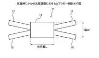
図2は、実施例にかかる光変調器におけるカプラの一例を示す図である。図2に示すように、カプラ11は、第1入射導波路12、第2入射導波路13、分岐部14、第1出射導波路15及び第2出射導波路16を備えている。第1入射導波路12、第2入射導波路13、第1出射導波路15及び第2出射導波路16は、分岐部14に連結されている。 FIG. 2 is a diagram illustrating an example of a coupler in the optical modulator according to the embodiment. As shown in FIG. 2, the
第1入射導波路12及び第2入射導波路13は、図示しない前段の光デバイスや光回路から伝達されてくる光信号を分岐部14へ導く。分岐部14は、第1入射導波路12から入力する光信号を分岐させて第1出射導波路15と第2出射導波路16とへ出力する。あるいは、分岐部14は、第1入射導波路12から入力する光信号と第2入射導波路13から入力する光信号とを結合し、その結合光を分岐させて第1出射導波路15と第2出射導波路16とへ出力する。第1出射導波路15及び第2出射導波路16は、分岐部14から出力される光信号を図示しない後段の光デバイスや光回路へ導く。 The first incident waveguide 12 and the
カプラ11では、対称モードの光信号と非対称モードの光信号とが伝搬する。カプラ11の分岐比は、カプラ11を伝搬する対称モードの光信号と非対称モードの光信号との位相差により決まる。この位相差は、カプラ11の作用長L、すなわち分岐部14の長さまたは、カプラ11の幅Wによって決まる。つまり、カプラ11の分岐比は、カプラ11の作用長L、すなわち分岐部14の長さ、またはカプラ11の幅Wによって決まる。 In the
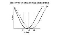
図3は、図2に示すカプラの分岐比の作用長依存性を示す特性図である。図3に示すように、カプラ11の分岐比、すなわちカプラ11において第1出射導波路15へ出力される光信号と第2出射導波路16へ出力される光信号との強度比は、カプラ11の作用長L、すなわち分岐部14の長さに依存する。 FIG. 3 is a characteristic diagram showing the dependence of the branching ratio of the coupler shown in FIG. 2 on the action length. As shown in FIG. 3, the branching ratio of the
図4は、図2に示すカプラの分岐比の波長依存性を示す特性図である。図4に示すように、カプラ11の作用長Lを適当に選択することによって、作用長LがL1であるときとL2であるときとで、光信号の波長の変化に対するカプラ11の分岐比の変化の傾向が反対の関係になる。 FIG. 4 is a characteristic diagram showing the wavelength dependence of the branching ratio of the coupler shown in FIG. As shown in FIG. 4, by appropriately selecting the working length L of the
ここで、L1は、例えば、図3に示す特性図において、光信号の波長がλbであるときにカプラ11の分岐比が極小となるときの作用長よりも短くてもよい。そして、L2(L1<L2)は、例えば、図3に示す特性図において、光信号の波長がλa(λa<λb)であるときにカプラ11の分岐比が極小となるときの作用長よりも長くてもよい。 Here, for example, L1 may be shorter than the working length when the branching ratio of the
例えば、図1に示す光変調器1において、第1カプラ2または第2カプラ5として図2に示すカプラ11を用いることができる。この場合、例えば、第1カプラ2の作用長をL1とし、第2カプラ5の作用長をL2としてもよいし、その反対でもよい。 For example, in the
図1に示す光変調器1によれば、第1カプラ2で2分岐にされて第1カプラ2から出力される2つの光信号が、第1マッハツェンダ型干渉計3または第2マッハツェンダ型干渉計4を経由した後、第2カプラ5で結合される。それによって、第2カプラ5で2分岐にされて第2カプラ5から出力される光信号の、第1カプラ2への入力光に対するロスを小さくすることができる。 According to the
また、図1に示す光変調器1によれば、第1カプラ2の作用長L1と第2カプラ5の作用長L2とを適当に選択することによって、第1カプラ2の分岐比の波長依存性が第2カプラ5の分岐比の波長依存性によって相殺される。それによって、波長依存性のない光変調器1が得られる。図1に示す光変調器1によれば、光変調器1への入力光に対して、例えばQPSK(Quadrature Phase Shift Keying)変調を行うことができる。 Further, according to the
なお、カプラ11は、図2に示すように対称の構造であってもよいし、非対称の構造であってもよい。カプラ11が対称の構造である場合、分岐部14に連結される第1入射導波路12と第2入射導波路13との幅、及び第1出射導波路15と第2出射導波路16との幅が、それぞれ同じになる。それによって、カプラ11の設計が容易になり、製造時のプロセスばらつきが低減される。また、第1入射導波路12、第2入射導波路13、第1出射導波路15または第2出射導波路16は、図2に示すように直線状であってもいし、曲線状であってもよい。 The
図1に示す光変調器1において、第1カプラ2、第1マッハツェンダ型干渉計3、第2マッハツェンダ型干渉計4及び第2カプラ5は、同一の電気光学結晶基板に形成されていてもよい。電気光学結晶の一例として、例えばLiNbO3(LN)結晶やLiTaO2結晶を挙げることができる。LN結晶やLiTaO2結晶からなる同一の電気光学結晶基板に光変調器1を形成することによって、生産性が高く、小型で低コストの光変調器を得ることができる。In the
LN結晶やLiTaO2結晶からなる基板を用いる場合、光変調器1は以下のようにして作製される。まず、結晶基板上の一部にTiなどの金属膜を形成し、熱拡散させることによって、結晶基板上に光導波路を形成する。あるいは、結晶基板に対してパターニングした後、例えば安息香酸中でプロトン交換することによって、光導波路を形成してもよい。しかる後、平行な2本の光導波路の近傍または上に信号電極及び接地電極を形成する。When using a substrate made of LN crystal or LiTaO2 crystal, the
LN基板には、例えばXカット基板やZカット基板がある。例えば、ZカットLN基板を用いる場合、光導波路の上に信号電極及び接地電極が配置される。そして、Z方向の電界による光導波路の屈折率変化を利用して、平行な2本の光導波路を伝搬する2つの光信号に位相差が生じる。LN基板と信号電極及び接地電極との間には、バッファ層が設けられる。バッファ層があることによって、光信号が信号電極及び接地電極に吸収されずに光導波路中を伝搬することができる。 Examples of the LN substrate include an X cut substrate and a Z cut substrate. For example, when using a Z-cut LN substrate, a signal electrode and a ground electrode are disposed on the optical waveguide. Then, using the change in the refractive index of the optical waveguide caused by the electric field in the Z direction, a phase difference occurs between the two optical signals propagating through the two parallel optical waveguides. A buffer layer is provided between the LN substrate, the signal electrode, and the ground electrode. Due to the presence of the buffer layer, the optical signal can propagate through the optical waveguide without being absorbed by the signal electrode and the ground electrode.
バッファ層の一例として、例えば厚さが0.2μm〜2μm程度のSiO2膜やTiO2膜、またはSiO2やTiO2を混合したものを含む膜が挙げられる。なお、第1マッハツェンダ型干渉計3及び第2マッハツェンダ型干渉計4をLN結晶やLiTaO2結晶などの電気光学結晶からなる光導波路で作製し、第1カプラ2及び第2カプラ5を例えば石英系光導波路で作製してもよい。As an example of the buffer layer, for example, a SiO2 film having a thickness of about 0.2 μm to2 μm, a TiO2 film, or a film containing a mixture of SiO2 and TiO2 can be cited. The first Mach-
例えば、光変調器1において、信号電極と接地電極とが、それぞれの終端が抵抗によって接続された進行波電極になっていてもよい。この場合、入力側からマイクロ波信号を印加し、電極の断面形状を変化させてマイクロ波の実効屈折率を制御し、光とマイクロ波との速度を整合させることによって、高速の光応答特性を得ることができる。 For example, in the
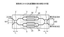
図5は、実施例にかかる光変調器の別の例を示す図である。図5に示す光変調器21は、図1に示す光変調器1において、第1マッハツェンダ型干渉計3及び第2マッハツェンダ型干渉計4のそれぞれの平行な光導波路部分がさらにマッハツェンダ型干渉計となっているものである。 FIG. 5 is a diagram illustrating another example of the optical modulator according to the embodiment. The
すなわち、第1マッハツェンダ型干渉計3の2本の平行な光導波路部分において、一方の光導波路部分に第3マッハツェンダ型干渉計22が形成されており、他方の光導波路部分に第4マッハツェンダ型干渉計23が形成されている。第3マッハツェンダ型干渉計22及び第4マッハツェンダ型干渉計23において、光変調器21への入力光に対してQPSK変調を行うことができる。 That is, in the two parallel optical waveguide portions of the first Mach-
また、第2マッハツェンダ型干渉計4の2本の平行な光導波路部分において、一方の光導波路部分に第5マッハツェンダ型干渉計24が形成されており、他方の光導波路部分に第6マッハツェンダ型干渉計25が形成されている。第5マッハツェンダ型干渉計24及び第6マッハツェンダ型干渉計25において、光変調器21への入力光に対してQPSK変調を行うことができる。 Further, in two parallel optical waveguide portions of the second Mach-Zehnder interferometer 4, a fifth Mach-
そして、第2カプラ5により、第1マッハツェンダ型干渉計3から出力される光信号と第2マッハツェンダ型干渉計4から出力される光信号とを結合することによって、光変調器21への入力光に対して16QAM(QAM:Quadrature Amplitude Modulation、直角位相振幅変調)を行うことができる。図6に、16QAM信号のコンスタレーションマップを示す。 Then, the optical signal output from the first Mach-
図5に示す光変調器21において、図1に示す光変調器1と同様に、第1カプラ2または第2カプラ5として図2に示すカプラ11を用いることができる。この場合、例えば、第1カプラ2の作用長を上述したL1とし、第2カプラ5の作用長を上述したL2としてもよいし、その反対でもよい。また、第1カプラ2の幅Wと第2カプラ5の幅Wとは、同じであってもよいし、異なっていてもよい。 In the
一例として、図5に示す光変調器21において、例えば第1カプラ2の分岐比をa、第2カプラ5の分岐比をb、第1マッハツェンダ型干渉計3の出力光の強度をA、及び第2マッハツェンダ型干渉計4の出力光の強度をBとする。この場合、第2カプラ5から出力される第5の出力光の強度は、次の(1)式で表される。また、第2カプラ5から出力される第6の出力光の強度は、次の(2)式で表される。 As an example, in the
abA+(1−a)(1−b)B ・・・(1)
a(1−b)A+(1−a)bB ・・・(2)abA + (1-a) (1-b) B (1)
a (1-b) A + (1-a) bB (2)
上記(1)式及び(2)式において、aが増大する波長ではbが減少する。従って、a及びbの波長特性を打ち消すことができる。第1カプラ2の分岐比は、作用長L1と幅Wに依存する。第2カプラ5の分岐比は、作用長L2と幅Wに依存する。例えば、L1/Wを28とし、L2/Wを50とすると、波長が1530nmである場合、aは0.63であり、bは0.70となる。また、波長が1610nmである場合、aは0.70であり、bは0.61となる。つまり、波長による出力光の強度の変動が抑えられる。従って、16QAMのコンスタレーションの波長特性が低減される。 In the above equations (1) and (2), b decreases at a wavelength where a increases. Therefore, the wavelength characteristics of a and b can be canceled out. The branching ratio of the
図5に示す光変調器21によれば、第1カプラ2で2分岐にされて第1カプラ2から出力される2つの光信号が、第1マッハツェンダ型干渉計3または第2マッハツェンダ型干渉計4を経由した後、第2カプラ5で結合される。それによって、第2カプラ5で2分岐にされて第2カプラ5から出力される光信号の、第1カプラ2への入力光に対するロスを小さくすることができる。従って、16QAM変調を行う光変調器21において、光変調器21から出力される光信号の、光変調器21へ入力する光信号に対するロスを小さくすることができる。 According to the
また、第1カプラ2の作用長L1と第2カプラ5の作用長L2とを適当に選択することによって、第1カプラ2の分岐比の波長依存性が第2カプラ5の分岐比の波長依存性によって相殺される。それによって、波長依存性のない光変調器1が得られる。 Further, by appropriately selecting the action length L1 of the
図7は、実施例にかかる光変調器の別の例を示す図である。図7に示す光変調器31は、図5に示す光変調器21において、第1カプラ2の作用長Lと第2カプラ5の作用長Lとを例えば同じ長さにし、第1カプラ2の幅W1と第2カプラ5の幅W2とを異なるようにしたものである。 FIG. 7 is a diagram illustrating another example of the optical modulator according to the embodiment. In the
上述したように、カプラの分岐比は、作用長と幅に依存する。作用長を一定とすると、カプラの分岐比のカプラ幅依存性を示す特性図は、例えば図3に示す特性図において横軸をカプラ幅Wとしたような特性図となる。また、カプラ幅Wを適当に選択した場合、カプラの分岐比の波長依存性を示す特性図は、例えば図4に示すような特性図となる。従って、第1カプラ2の幅W1と第2カプラ5の幅W2とを適当に選択することによって、光信号の波長の変化に対する第1カプラ2の分岐比の変化の傾向と、光信号の波長の変化に対する第2カプラ5の分岐比の変化の傾向とが反対の関係になる。 As described above, the branching ratio of the coupler depends on the action length and width. If the action length is constant, the characteristic diagram showing the coupler width dependency of the coupler branching ratio is a characteristic diagram in which, for example, the horizontal axis in the characteristic diagram shown in FIG. In addition, when the coupler width W is appropriately selected, the characteristic diagram showing the wavelength dependence of the coupler branching ratio is, for example, as shown in FIG. Accordingly, by appropriately selecting the width W1 of the
図7に示す光変調器31によれば、第1カプラ2の幅W1と第2カプラ5の幅W2とを異ならせることによって、波長依存性がなく、光変調器31から出力される光信号の、光変調器31へ入力する光信号に対するロスの小さい光変調器31が得られる。この光変調器31によって、16QAM変調を行うことができる。 According to the
図8は、実施例にかかる光変調器の別の例を示す図である。図8に示す光変調器41は、図5に示す光変調器21において、第2マッハツェンダ型干渉計4が図5に示す光変調器21の構成になっているものである。 FIG. 8 is a diagram illustrating another example of the optical modulator according to the embodiment. The
図8に示す光変調器41において、光変調器41への入力光を第1マッハツェンダ型干渉計3と第2マッハツェンダ型干渉計4とへ分岐させるカプラを第1カプラ2とする。また、第1マッハツェンダ型干渉計3の出力光と第2マッハツェンダ型干渉計4の出力光とを結合し、2分岐させて第5の出力光及び第6の出力光を出力するカプラを第2カプラ5とする。 In the
また、第2マッハツェンダ型干渉計4において、第2マッハツェンダ型干渉計4への入力光を2つのマッハツェンダ型干渉計対42,43へ分岐させるカプラを第3カプラ44とする。また、第2マッハツェンダ型干渉計4において、一方のマッハツェンダ型干渉計対42の出力光と他方のマッハツェンダ型干渉計対43の出力光とを結合し、2分岐させ、一方の出力光を第2カプラ5へ出力するカプラを第4カプラ45とする。 In the second Mach-Zehnder interferometer 4, a coupler that branches the input light to the second Mach-Zehnder interferometer 4 to the two Mach-Zehnder interferometer pairs 42 and 43 is referred to as a
図8に示す光変調器41において、図1に示す光変調器1と同様に、第1カプラ2、第2カプラ5、第3カプラ44及び第4カプラ45として図2に示すカプラ11を用いることができる。この場合、第1カプラ2の作用長と第2カプラ5の作用長とを適当に選択することによって、光信号の波長の変化に対する第1カプラ2の分岐比の変化の傾向と、光信号の波長の変化に対する第2カプラ5の分岐比の変化の傾向とが反対の関係になる。 In the
また、第3カプラ44の作用長と第4カプラ45の作用長とを適当に選択することによって、光信号の波長の変化に対する第3カプラ44の分岐比の変化の傾向と、光信号の波長の変化に対する第4カプラ45の分岐比の変化の傾向とが反対の関係になる。なお、第1カプラ2、第2カプラ5、第3カプラ44及び第4カプラ45のそれぞれの作用長を選択する代わりに、図7に示す光変調器31のように、第1カプラ2、第2カプラ5、第3カプラ44及び第4カプラ45のそれぞれの幅を選択するようにしてもよい。 Further, by appropriately selecting the working length of the
図8に示す光変調器41によれば、波長依存性がなく、光変調器41から出力される光信号の、光変調器41へ入力する光信号に対するロスの小さい光変調器41が得られる。この光変調器41によって、64QAM変調を行うことができる。なお、図8に示す光変調器41において、第1カプラ2、第2カプラ5、第3カプラ44及び第4カプラ45の作用長を適当に選択する代わりに、幅を適当に選択してもよい。 According to the
図9は、実施例にかかる光変調器におけるカプラの別の例を示す図である。図9に示すように、カプラ51は、2つの光導波路52,53が交差する交差導波路型のものである。カプラ51において、交差する2つの光導波路52,53のなす角度をθとする。 FIG. 9 is a diagram illustrating another example of the coupler in the optical modulator according to the embodiment. As shown in FIG. 9, the
カプラの分岐比の角度θ依存性を示す特性図は、例えば図3に示す特性図において横軸を角度θとしたような特性図となる。また、角度θを適当に選択した場合、カプラの分岐比の波長依存性を示す特性図は、例えば図4に示すような特性図となる。従って、例えば図1に示す光変調器1において、第1カプラ2または第2カプラ5として図9に示す交差導波路型のカプラ51を用いることができる。 The characteristic diagram showing the dependence of the branching ratio of the coupler on the angle θ is, for example, a characteristic diagram in which the horizontal axis is the angle θ in the characteristic diagram shown in FIG. In addition, when the angle θ is appropriately selected, the characteristic diagram showing the wavelength dependence of the branching ratio of the coupler is, for example, a characteristic diagram as shown in FIG. Therefore, for example, in the
第1カプラ2(交差導波路型)の角度θと第2カプラ5(交差導波路型)の角度θとを適当に選択することによって、光信号の波長の変化に対する第1カプラ2の分岐比の変化の傾向と、光信号の波長の変化に対する第2カプラ5の分岐比の変化の傾向とが反対の関係になる。例えば図5に示す光変調器21においても同様である。また、例えば図8に示す光変調器41においては、第2マッハツェンダ型干渉計4内の第3カプラ44及び第4カプラ45についても同様である。 By appropriately selecting the angle θ of the first coupler 2 (cross waveguide type) and the angle θ of the second coupler 5 (cross waveguide type), the branching ratio of the
図9に示すカプラ51によれば、このカプラ51を用いた光変調器1,21,31,41において、波長依存性がなく、光変調器1,21,31,41から出力される光信号の、光変調器1,21,31,41へ入力する光信号に対するロスの小さい光変調器1,21,31,41が得られる。 According to the
図10は、実施例にかかる光変調器を用いた光送信装置の一例を示す図である。図10に示すように、光送信装置61は、光変調器モジュール62及びデータ生成回路63を備えている。光変調器モジュール62は、例えば金属製のパッケージ内に上述したいずれかの光変調器1,21,31,41のチップを収めたものである。データ生成回路63は、光変調器のチップ上の電極に供給する信号を生成する。 FIG. 10 is a diagram illustrating an example of an optical transmission device using the optical modulator according to the embodiment. As illustrated in FIG. 10, the
光変調器モジュール62には、例えば高周波用同軸コネクタがパッケージの壁を貫通するように取り付けられている。この高周波用同軸コネクタを利用して、データ生成回路63のドライバアンプからの出力電気信号が光変調器のチップ上の電極に供給される。光変調器モジュール62によって変調された光信号は、例えば光変調器モジュール62から、例えば光変調器モジュール62に接続された光ファイバ64へ出力される。 For example, a high frequency coaxial connector is attached to the
図10に示す光送信装置61によれば、光変調器1,21,31,41で発生するロスが小さい。従って、光送信装置61は、高い強度の光信号を送信することができる。 According to the
なお、図1に示す光変調器1、図5に示す光変調器21、図7に示す光変調器31および図8に示す光変調器41において、各カプラ2,5,44,45の作用長L及び幅Wの両方を適当に選択するようにしてもよい。また、同一の光変調器内に、作用長Lを適当に選択したカプラや、幅Wを適当に選択したカプラや、作用長Lと幅Wの両方を適当に選択したカプラが混在していてもよい。また、図5に示す光変調器21と図8に示す光変調器41との関係から明らかなように、図5に示す光変調器21の構成を入れ子式にしていくことによって、64QAMを超えるQAM変調を行うことができる。 In the
上述した各実施例に関し、さらに以下の付記を開示する。 The following additional notes are disclosed with respect to each of the embodiments described above.
(付記1)入力光を2分岐させて第1の出力光及び第2の出力光を出力する第1カプラと、前記第1カプラから出力される前記第1の出力光の強度を変調して第3の出力光を出力する第1マッハツェンダ型干渉計と、前記第1カプラから出力される前記第2の出力光の強度を変調して第4の出力光を出力する第2マッハツェンダ型干渉計と、前記第1マッハツェンダ型干渉計から出力される前記第3の出力光及び前記第2マッハツェンダ型干渉計から出力される前記第4の出力光を結合し、結合された光を2分岐させて第5の出力光及び第6の出力光を出力する第2カプラと、を備え、前記第1カプラの分岐部の作用長及び前記第2カプラの分岐部の作用長は、前記第1カプラの分岐比の波長依存性と前記第2カプラの分岐比の波長依存性とが反対の関係になる長さであることを特徴とする光変調器。(Supplementary Note 1) A first coupler that splits input light into two to output first output light and second output light, and modulates the intensity of the first output light output from the first coupler. A first Mach-Zehnder interferometer that outputs third output light, and a second Mach-Zehnder interferometer that modulates the intensity of the second output light output from the first coupler and outputs fourth output light. And combining the third output light output from the first Mach-Zehnder interferometer and the fourth output light output from the second Mach-Zehnder interferometer, and splitting the combined light into two. A second coupler that outputs a fifth output light and a sixth output light, and the action length of the branch part of the first coupler and the action length of the branch part of the second coupler are the same as those of the first coupler. The wavelength dependence of the branching ratio and the wavelength dependence of the branching ratio of the second coupler Optical modulator, characterized in that the length of the opposite relationship.
(付記2)入力光を2分岐させて第1の出力光及び第2の出力光を出力する第1カプラと、前記第1カプラから出力される前記第1の出力光の強度を変調して第3の出力光を出力する第1マッハツェンダ型干渉計と、前記第1カプラから出力される前記第2の出力光の強度を変調して第4の出力光を出力する第2マッハツェンダ型干渉計と、前記第1マッハツェンダ型干渉計から出力される前記第3の出力光及び前記第2マッハツェンダ型干渉計から出力される前記第4の出力光を結合し、結合された光を2分岐させて第5の出力光及び第6の出力光を出力する第2カプラと、を備え、前記第1カプラの分岐部の幅及び前記第2カプラの分岐部の幅は、前記第1カプラの分岐比の波長依存性と前記第2カプラの分岐比の波長依存性とが反対の関係になる幅であることを特徴とする光変調器。(Supplementary Note 2) A first coupler that divides input light into two to output first output light and second output light, and modulates the intensity of the first output light output from the first coupler. A first Mach-Zehnder interferometer that outputs third output light, and a second Mach-Zehnder interferometer that modulates the intensity of the second output light output from the first coupler and outputs fourth output light. And combining the third output light output from the first Mach-Zehnder interferometer and the fourth output light output from the second Mach-Zehnder interferometer, and splitting the combined light into two. A second coupler that outputs a fifth output light and a sixth output light, wherein the branch width of the first coupler and the branch width of the second coupler are the branching ratio of the first coupler. Is opposite to the wavelength dependency of the branching ratio of the second coupler. Optical modulator, characterized in that the width becomes engaged.
(付記3)入力光を2分岐させて第1の出力光及び第2の出力光を出力する第1カプラと、前記第1カプラから出力される前記第1の出力光の強度を変調して第3の出力光を出力する第1マッハツェンダ型干渉計と、前記第1カプラから出力される前記第2の出力光の強度を変調して第4の出力光を出力する第2マッハツェンダ型干渉計と、前記第1マッハツェンダ型干渉計から出力される前記第3の出力光及び前記第2マッハツェンダ型干渉計から出力される前記第4の出力光を結合し、結合された光を2分岐させて第5の出力光及び第6の出力光を出力する第2カプラと、を備え、前記第1カプラ及び前記第2カプラは交差する2つの光導波路を有し、前記第1カプラの前記2つの光導波路のなす角度及び前記第2カプラの前記2つの光導波路のなす角度は、前記第1カプラの分岐比の波長依存性と前記第2カプラの分岐比の波長依存性とが反対の関係になる角度であることを特徴とする光変調器。(Supplementary Note 3) A first coupler that divides input light into two to output first output light and second output light, and modulates the intensity of the first output light output from the first coupler. A first Mach-Zehnder interferometer that outputs third output light, and a second Mach-Zehnder interferometer that modulates the intensity of the second output light output from the first coupler and outputs fourth output light. And combining the third output light output from the first Mach-Zehnder interferometer and the fourth output light output from the second Mach-Zehnder interferometer, and splitting the combined light into two. A second coupler that outputs a fifth output light and a sixth output light, wherein the first coupler and the second coupler have two optical waveguides that intersect, and the two couplers of the first coupler The angle formed by the optical waveguide and the two lights of the second coupler Angle of waveguide, the optical modulator, characterized in that the wavelength dependency of the branching ratio of the second coupler and the wavelength dependence of the branching ratio of the first coupler is an angle in opposite relationship.
(付記4)前記第1マッハツェンダ型干渉計の平行に配置された各光導波路部分がさらにマッハツェンダ型干渉計を有し、前記第2マッハツェンダ型干渉計の平行に配置された各光導波路部分がさらにマッハツェンダ型干渉計を有し、前記入力光に対して直角位相振幅変調を行うことを特徴とする付記1〜3のいずれか一つに記載の光変調器。(Supplementary Note 4) Each optical waveguide portion arranged in parallel with the first Mach-Zehnder interferometer further includes a Mach-Zehnder type interferometer, and each optical waveguide portion arranged in parallel with the second Mach-Zehnder interferometer further 4. The optical modulator according to any one of
(付記5)前記第1カプラ、前記第2カプラ、前記第1マッハツェンダ型干渉計及び前記第2マッハツェンダ型干渉計は、同一の電気光学結晶基板に形成されていることを特徴とする付記1〜4のいずれか一つに記載の光変調器。(Supplementary Note 5) The first coupler, the second coupler, the first Mach-Zehnder interferometer, and the second Mach-Zehnder interferometer are formed on the same electro-optic crystal substrate. 5. The optical modulator according to any one of 4.
(付記6)前記電気光学結晶は、LiNbO3結晶であることを特徴とする付記5に記載の光変調器。(Supplementary note 6) The optical modulator according to
(付記7)前記電気光学結晶は、LiTaO2結晶であることを特徴とする付記5に記載の光変調器。(Supplementary note 7) The optical modulator according to
1,21,31,41 光変調器
2 第1カプラ
3 第1マッハツェンダ型干渉計
4 第2マッハツェンダ型干渉計
5 第2カプラ1, 21, 31, 41
Claims (4)
Translated fromJapanese前記第1カプラから出力される前記第1の出力光の強度を変調して第3の出力光を出力する第1マッハツェンダ型干渉計と、
前記第1カプラから出力される前記第2の出力光の強度を変調して第4の出力光を出力する第2マッハツェンダ型干渉計と、
前記第1マッハツェンダ型干渉計から出力される前記第3の出力光及び前記第2マッハツェンダ型干渉計から出力される前記第4の出力光を結合し、結合された光を2分岐させて第5の出力光及び第6の出力光を出力する第2カプラと、
を備え、
前記第1カプラの分岐比aと、前記第2カプラの分岐比bと、前記第1マッハツェンダ型干渉計の出力光の強度Aと、前記第2マッハツェンダ型干渉計の出力光の強度Bとしたときの、
前記第2カプラの一方の出力光の強度:abA+(1−a)(1−b)B
前記第2カプラの他方の出力光の強度:a(1−b)A+(1−a)bB
との関係に基づき、前記第1カプラと前記第2カプラは、前記第1カプラの分岐比の波長依存性と前記第2カプラの分岐比の波長依存性とが反対の関係になる作用長としたことを特徴とする光変調器。A first coupler that splits the input light into two and outputs the first output light and the second output light;
A first Mach-Zehnder interferometer that modulates the intensity of the first output light output from the first coupler and outputs a third output light;
A second Mach-Zehnder interferometer that modulates the intensity of the second output light output from the first coupler and outputs a fourth output light;
The third output light output from the first Mach-Zehnder interferometer and the fourth output light output from the second Mach-Zehnder interferometer are combined, and the combined light is split into two to provide a fifth output light. A second coupler that outputs the output light and the sixth output light;
With
The branch ratioa of the first coupler, the branch ratiob of the second coupler, the output light intensityA of the first Mach-Zehnder interferometer, and the output light intensityB of the second Mach-Zehnder interferometer. When
Intensity of one output light of the second coupler: abA + (1-a) (1-b) B
The intensity of the other output light of the second coupler: a (1-b) A + (1-a) bB
Based on the relationship between, the said first coupler the second coupler includesa working length and the wavelength dependence of the branching ratio ofthe second coupler and the wavelength dependence of the branching ratio ofthe first coupler is opposite relationship An optical modulator characterizedby that.
前記第1カプラから出力される前記第1の出力光の強度を変調して第3の出力光を出力する第1マッハツェンダ型干渉計と、
前記第1カプラから出力される前記第2の出力光の強度を変調して第4の出力光を出力する第2マッハツェンダ型干渉計と、
前記第1マッハツェンダ型干渉計から出力される前記第3の出力光及び前記第2マッハツェンダ型干渉計から出力される前記第4の出力光を結合し、結合された光を2分岐させて第5の出力光及び第6の出力光を出力する第2カプラと、
を備え、
前記第1カプラ及び前記第2カプラは交差する2つの光導波路を有し、前記第1カプラの前記2つの光導波路のなす角度及び前記第2カプラの前記2つの光導波路のなす角度は、
前記第1カプラの分岐比aと、前記第2カプラの分岐比bと、前記第1マッハツェンダ型干渉計の出力光の強度Aと、前記第2マッハツェンダ型干渉計の出力光の強度Bとしたときの、
前記第2カプラの一方の出力光の強度:abA+(1−a)(1−b)B
前記第2カプラの他方の出力光の強度:a(1−b)A+(1−a)bB
との関係に基づき、前記第1カプラと前記第2カプラは、前記第1カプラの分岐比の波長依存性と前記第2カプラの分岐比の波長依存性とが反対の関係になる角度であることを特徴とする光変調器。A first coupler that splits the input light into two and outputs the first output light and the second output light;
A first Mach-Zehnder interferometer that modulates the intensity of the first output light output from the first coupler and outputs a third output light;
A second Mach-Zehnder interferometer that modulates the intensity of the second output light output from the first coupler and outputs a fourth output light;
The third output light output from the first Mach-Zehnder interferometer and the fourth output light output from the second Mach-Zehnder interferometer are combined, and the combined light is split into two to provide a fifth output light. A second coupler that outputs the output light and the sixth output light;
With
The first coupler and the second coupler have two intersecting optical waveguides, and an angle formed by the two optical waveguides of the first coupler and an angle formed by the two optical waveguides of the second coupler are:
The branch ratio a of the first coupler, the branch ratio b of the second coupler, the output light intensity A of the first Mach-Zehnder interferometer, and the output light intensity B of the second Mach-Zehnder interferometer. When
Intensity of one output light of the second coupler: abA + (1-a) (1-b) B
The intensity of the other output light of the second coupler: a (1-b) A + (1-a) bB
Based on the relationship, the first coupler and the second coupler have an angle at which the wavelength dependence of the branching ratio of the first coupler and the wavelength dependence of the branching ratio of the second coupler are opposite to each other. An optical modulator characterized by that.
前記第2マッハツェンダ型干渉計の平行に配置された各光導波路部分がさらにマッハツェンダ型干渉計を有し、
前記入力光に対して直角位相振幅変調を行うことを特徴とする請求項1または2に記載の光変調器。Each optical waveguide portion arranged in parallel with the first Mach-Zehnder interferometer further has a Mach-Zehnder interferometer,
Each optical waveguide portion arranged in parallel with the second Mach-Zehnder interferometer further has a Mach-Zehnder interferometer,
The optical modulator according to claim 1, wherein quadrature amplitude modulation is performed on the input light.
Priority Applications (3)
| Application Number | Priority Date | Filing Date | Title |
|---|---|---|---|
| JP2012061875AJP6047899B2 (en) | 2012-03-19 | 2012-03-19 | Light modulator |
| US13/761,526US20130243363A1 (en) | 2012-03-19 | 2013-02-07 | Optical modulator |
| US14/704,072US9568801B2 (en) | 2012-03-19 | 2015-05-05 | Optical modulator |
Applications Claiming Priority (1)
| Application Number | Priority Date | Filing Date | Title |
|---|---|---|---|
| JP2012061875AJP6047899B2 (en) | 2012-03-19 | 2012-03-19 | Light modulator |
Publications (2)
| Publication Number | Publication Date |
|---|---|
| JP2013195643A JP2013195643A (en) | 2013-09-30 |
| JP6047899B2true JP6047899B2 (en) | 2016-12-21 |
Family
ID=49157729
Family Applications (1)
| Application Number | Title | Priority Date | Filing Date |
|---|---|---|---|
| JP2012061875AActiveJP6047899B2 (en) | 2012-03-19 | 2012-03-19 | Light modulator |
Country Status (2)
| Country | Link |
|---|---|
| US (2) | US20130243363A1 (en) |
| JP (1) | JP6047899B2 (en) |
Cited By (1)
| Publication number | Priority date | Publication date | Assignee | Title |
|---|---|---|---|---|
| US10806889B2 (en) | 2008-06-05 | 2020-10-20 | ResMed Pty Ltd | Treatment of respiratory conditions |
Families Citing this family (10)
| Publication number | Priority date | Publication date | Assignee | Title |
|---|---|---|---|---|
| JP7106996B2 (en)* | 2018-06-01 | 2022-07-27 | 富士通オプティカルコンポーネンツ株式会社 | optical device |
| JP6702307B2 (en)* | 2015-03-30 | 2020-06-03 | 日本電気株式会社 | Optical circuit and optical switch using the same |
| JP2017211504A (en)* | 2016-05-26 | 2017-11-30 | 住友大阪セメント株式会社 | Optical modulator |
| JP6233480B1 (en)* | 2016-09-20 | 2017-11-22 | 富士通オプティカルコンポーネンツ株式会社 | Light modulator |
| US10809592B2 (en) | 2017-08-18 | 2020-10-20 | Xanadu Quantum Technologies Inc. | Methods and apparatus for producing highly tunable squeezed light |
| WO2019148264A1 (en)* | 2018-02-05 | 2019-08-08 | Gc Photonics Inc. | Variable optical filter |
| US20210223657A1 (en)* | 2018-04-30 | 2021-07-22 | President And Fellows Of Harvard College | Active photonic networks on integrated lithium niobate platforms |
| CN114365033B (en)* | 2019-09-13 | 2025-05-16 | 日本电信电话株式会社 | IQ Optical Modulator |
| CN111487719A (en)* | 2020-04-22 | 2020-08-04 | 电子科技大学 | A silicon-based lithium niobate polarization-independent light modulator based on mode conversion |
| JP7480648B2 (en)* | 2020-09-14 | 2024-05-10 | 富士通オプティカルコンポーネンツ株式会社 | Optical devices and optical transceivers |
Family Cites Families (12)
| Publication number | Priority date | Publication date | Assignee | Title |
|---|---|---|---|---|
| FR2680418B1 (en)* | 1991-08-13 | 1995-01-20 | Corning Inc | ACHROMATIC DIVIDER IN INTEGRATED OPTICS AND COUPLER OF M INPUTS TO N OUTPUTS INCORPORATING SUCH A DIVIDER. |
| US5278923A (en)* | 1992-09-02 | 1994-01-11 | Harmonic Lightwaves, Inc. | Cascaded optical modulation system with high linearity |
| US6091864A (en)* | 1997-04-10 | 2000-07-18 | Ortel Corporation | Linear optical modulator for providing chirp-free optical signals |
| WO2005003852A1 (en)* | 2003-07-04 | 2005-01-13 | Nippon Telegraph And Telephone Corporation | Interference optical switch and variable optical attenuator |
| JP4631006B2 (en)* | 2005-08-24 | 2011-02-16 | 独立行政法人情報通信研究機構 | Automatic adjustment system for FSK modulator |
| WO2008026326A1 (en)* | 2006-08-30 | 2008-03-06 | Hitachi Communication Technologies, Ltd. | Optical modulator |
| JP5045416B2 (en)* | 2007-12-17 | 2012-10-10 | 富士通株式会社 | Optical waveguide device and optical device using the same |
| JP2010066663A (en)* | 2008-09-12 | 2010-03-25 | Fujitsu Ltd | Optical device and optical transmitter |
| US8542961B2 (en)* | 2008-10-31 | 2013-09-24 | Hewlett-Packard Development Company, L.P. | Optical beam couplers and splitters |
| JP5326624B2 (en)* | 2009-02-10 | 2013-10-30 | 富士通オプティカルコンポーネンツ株式会社 | Light modulator |
| JP5161370B2 (en)* | 2009-07-10 | 2013-03-13 | 日本電信電話株式会社 | Light modulator |
| US8532447B1 (en)* | 2011-04-19 | 2013-09-10 | Emcore Corporation | Multi-mode interference splitter/combiner with adjustable splitting ratio |
- 2012
- 2012-03-19JPJP2012061875Apatent/JP6047899B2/enactiveActive
- 2013
- 2013-02-07USUS13/761,526patent/US20130243363A1/ennot_activeAbandoned
- 2015
- 2015-05-05USUS14/704,072patent/US9568801B2/enactiveActive
Cited By (5)
| Publication number | Priority date | Publication date | Assignee | Title |
|---|---|---|---|---|
| US10806889B2 (en) | 2008-06-05 | 2020-10-20 | ResMed Pty Ltd | Treatment of respiratory conditions |
| US11229766B2 (en) | 2008-06-05 | 2022-01-25 | ResMed Pty Ltd | Treatment of respiratory conditions |
| US11247019B2 (en) | 2008-06-05 | 2022-02-15 | ResMed Pty Ltd | Treatment of respiratory conditions |
| US11433213B2 (en) | 2008-06-05 | 2022-09-06 | ResMed Pty Ltd | Treatment of respiratory conditions |
| US11878123B2 (en) | 2008-06-05 | 2024-01-23 | ResMed Pty Ltd | Treatment of respiratory conditions |
Also Published As
| Publication number | Publication date |
|---|---|
| JP2013195643A (en) | 2013-09-30 |
| US20130243363A1 (en) | 2013-09-19 |
| US20150234252A1 (en) | 2015-08-20 |
| US9568801B2 (en) | 2017-02-14 |
Similar Documents
| Publication | Publication Date | Title |
|---|---|---|
| JP6047899B2 (en) | Light modulator | |
| US9081216B2 (en) | Optical device having optical modulators | |
| JP5233765B2 (en) | Optical device | |
| JP4842987B2 (en) | Optical device | |
| US9557624B2 (en) | Optical modulator and optical transmitter | |
| JP5092573B2 (en) | Optical waveguide device | |
| JP5267476B2 (en) | Optical device and optical transmitter | |
| JP6136473B2 (en) | Light modulator | |
| CN103091869B (en) | Integrated coherent light communication electrooptical modulator structure | |
| JP6186713B2 (en) | Optical modulator and optical transmitter | |
| JP5045416B2 (en) | Optical waveguide device and optical device using the same | |
| JP5076726B2 (en) | Optical modulator and optical transmitter | |
| US9377665B2 (en) | Optical modulator having a 2×2 coupler | |
| JP4587762B2 (en) | Light modulation element module | |
| JP2008009314A (en) | Optical waveguide element, optical modulator, and optical communication device | |
| JP4701428B2 (en) | Driving circuit for traveling wave electrode, optical modulation system using the same, optical information communication system, and driving method for traveling wave electrode | |
| JP5239610B2 (en) | Mach-Zehnder optical modulator | |
| CN118348699A (en) | Coherent optical modulator chip and coherent modulator | |
| WO2024093732A1 (en) | Optical-mode modulation device and photonic chip | |
| JP2010060986A (en) | Optical element |
Legal Events
| Date | Code | Title | Description |
|---|---|---|---|
| A621 | Written request for application examination | Free format text:JAPANESE INTERMEDIATE CODE: A621 Effective date:20141201 | |
| A977 | Report on retrieval | Free format text:JAPANESE INTERMEDIATE CODE: A971007 Effective date:20150819 | |
| A131 | Notification of reasons for refusal | Free format text:JAPANESE INTERMEDIATE CODE: A131 Effective date:20150901 | |
| A521 | Request for written amendment filed | Free format text:JAPANESE INTERMEDIATE CODE: A523 Effective date:20151102 | |
| A02 | Decision of refusal | Free format text:JAPANESE INTERMEDIATE CODE: A02 Effective date:20160510 | |
| A521 | Request for written amendment filed | Free format text:JAPANESE INTERMEDIATE CODE: A523 Effective date:20160810 | |
| A911 | Transfer to examiner for re-examination before appeal (zenchi) | Free format text:JAPANESE INTERMEDIATE CODE: A911 Effective date:20160818 | |
| TRDD | Decision of grant or rejection written | ||
| A01 | Written decision to grant a patent or to grant a registration (utility model) | Free format text:JAPANESE INTERMEDIATE CODE: A01 Effective date:20161025 | |
| A61 | First payment of annual fees (during grant procedure) | Free format text:JAPANESE INTERMEDIATE CODE: A61 Effective date:20161107 | |
| R150 | Certificate of patent or registration of utility model | Ref document number:6047899 Country of ref document:JP Free format text:JAPANESE INTERMEDIATE CODE: R150 | |
| S531 | Written request for registration of change of domicile | Free format text:JAPANESE INTERMEDIATE CODE: R313531 | |
| S533 | Written request for registration of change of name | Free format text:JAPANESE INTERMEDIATE CODE: R313533 | |
| R350 | Written notification of registration of transfer | Free format text:JAPANESE INTERMEDIATE CODE: R350 |