JP6038843B2 - Device comprising at least one intermixing layer - Google Patents
Device comprising at least one intermixing layerDownload PDFInfo
- Publication number
- JP6038843B2 JP6038843B2JP2014129133AJP2014129133AJP6038843B2JP 6038843 B2JP6038843 B2JP 6038843B2JP 2014129133 AJP2014129133 AJP 2014129133AJP 2014129133 AJP2014129133 AJP 2014129133AJP 6038843 B2JP6038843 B2JP 6038843B2
- Authority
- JP
- Japan
- Prior art keywords
- layer
- carbide
- oxide
- intermixing
- sulfide
- Prior art date
- Legal status (The legal status is an assumption and is not a legal conclusion. Google has not performed a legal analysis and makes no representation as to the accuracy of the status listed.)
- Expired - Fee Related
Links
- 239000000463materialSubstances0.000claimsdescription140
- 229910052751metalInorganic materials0.000claimsdescription51
- 239000002184metalSubstances0.000claimsdescription51
- PXHVJJICTQNCMI-UHFFFAOYSA-NNickelChemical compound[Ni]PXHVJJICTQNCMI-UHFFFAOYSA-N0.000claimsdescription39
- BASFCYQUMIYNBI-UHFFFAOYSA-NplatinumChemical compound[Pt]BASFCYQUMIYNBI-UHFFFAOYSA-N0.000claimsdescription33
- 239000011651chromiumSubstances0.000claimsdescription27
- 239000010955niobiumSubstances0.000claimsdescription26
- PCHJSUWPFVWCPO-UHFFFAOYSA-NgoldChemical compound[Au]PCHJSUWPFVWCPO-UHFFFAOYSA-N0.000claimsdescription22
- 239000010931goldSubstances0.000claimsdescription22
- 239000010936titaniumSubstances0.000claimsdescription22
- KDLHZDBZIXYQEI-UHFFFAOYSA-NPalladiumChemical compound[Pd]KDLHZDBZIXYQEI-UHFFFAOYSA-N0.000claimsdescription20
- 229910052737goldInorganic materials0.000claimsdescription20
- -1hafnium nitrideChemical class0.000claimsdescription20
- 229910052741iridiumInorganic materials0.000claimsdescription18
- 239000011572manganeseSubstances0.000claimsdescription18
- 229910052804chromiumInorganic materials0.000claimsdescription17
- 229910052759nickelInorganic materials0.000claimsdescription17
- 229910052782aluminiumInorganic materials0.000claimsdescription16
- AMWRITDGCCNYAT-UHFFFAOYSA-Lhydroxy(oxo)manganese;manganeseChemical compound[Mn].O[Mn]=O.O[Mn]=OAMWRITDGCCNYAT-UHFFFAOYSA-L0.000claimsdescription16
- 229910052697platinumInorganic materials0.000claimsdescription16
- 239000010948rhodiumSubstances0.000claimsdescription16
- 229910052758niobiumInorganic materials0.000claimsdescription15
- 239000011135tinSubstances0.000claimsdescription15
- 229910052735hafniumInorganic materials0.000claimsdescription14
- 239000011777magnesiumSubstances0.000claimsdescription13
- 239000000203mixtureSubstances0.000claimsdescription13
- 229910052702rheniumInorganic materials0.000claimsdescription13
- 229910052707rutheniumInorganic materials0.000claimsdescription13
- 229910052710siliconInorganic materials0.000claimsdescription13
- 229910052719titaniumInorganic materials0.000claimsdescription13
- UQSXHKLRYXJYBZ-UHFFFAOYSA-NIron oxideChemical compound[Fe]=OUQSXHKLRYXJYBZ-UHFFFAOYSA-N0.000claimsdescription12
- XAGFODPZIPBFFR-UHFFFAOYSA-NaluminiumChemical compound[Al]XAGFODPZIPBFFR-UHFFFAOYSA-N0.000claimsdescription12
- 229910017052cobaltInorganic materials0.000claimsdescription12
- 239000010941cobaltSubstances0.000claimsdescription12
- GUTLYIVDDKVIGB-UHFFFAOYSA-Ncobalt atomChemical compound[Co]GUTLYIVDDKVIGB-UHFFFAOYSA-N0.000claimsdescription12
- 229910052748manganeseInorganic materials0.000claimsdescription11
- 229910052715tantalumInorganic materials0.000claimsdescription11
- 229910052721tungstenInorganic materials0.000claimsdescription11
- 229910052727yttriumInorganic materials0.000claimsdescription11
- PWHULOQIROXLJO-UHFFFAOYSA-NManganeseChemical compound[Mn]PWHULOQIROXLJO-UHFFFAOYSA-N0.000claimsdescription10
- GKOZUEZYRPOHIO-UHFFFAOYSA-Niridium atomChemical compound[Ir]GKOZUEZYRPOHIO-UHFFFAOYSA-N0.000claimsdescription10
- GUCVJGMIXFAOAE-UHFFFAOYSA-Nniobium atomChemical compound[Nb]GUCVJGMIXFAOAE-UHFFFAOYSA-N0.000claimsdescription10
- 229910052763palladiumInorganic materials0.000claimsdescription10
- 229910052718tinInorganic materials0.000claimsdescription10
- VWQVUPCCIRVNHF-UHFFFAOYSA-Nyttrium atomChemical compound[Y]VWQVUPCCIRVNHF-UHFFFAOYSA-N0.000claimsdescription10
- VYZAMTAEIAYCRO-UHFFFAOYSA-NChromiumChemical compound[Cr]VYZAMTAEIAYCRO-UHFFFAOYSA-N0.000claimsdescription9
- KJTLSVCANCCWHF-UHFFFAOYSA-NRutheniumChemical compound[Ru]KJTLSVCANCCWHF-UHFFFAOYSA-N0.000claimsdescription9
- XUIMIQQOPSSXEZ-UHFFFAOYSA-NSiliconChemical compound[Si]XUIMIQQOPSSXEZ-UHFFFAOYSA-N0.000claimsdescription9
- RTAQQCXQSZGOHL-UHFFFAOYSA-NTitaniumChemical compound[Ti]RTAQQCXQSZGOHL-UHFFFAOYSA-N0.000claimsdescription9
- 229910052796boronInorganic materials0.000claimsdescription9
- VBJZVLUMGGDVMO-UHFFFAOYSA-Nhafnium atomChemical compound[Hf]VBJZVLUMGGDVMO-UHFFFAOYSA-N0.000claimsdescription9
- TWNQGVIAIRXVLR-UHFFFAOYSA-Noxo(oxoalumanyloxy)alumaneChemical compoundO=[Al]O[Al]=OTWNQGVIAIRXVLR-UHFFFAOYSA-N0.000claimsdescription9
- WUAPFZMCVAUBPE-UHFFFAOYSA-Nrhenium atomChemical compound[Re]WUAPFZMCVAUBPE-UHFFFAOYSA-N0.000claimsdescription9
- 229910052703rhodiumInorganic materials0.000claimsdescription9
- 239000010703siliconSubstances0.000claimsdescription9
- GUVRBAGPIYLISA-UHFFFAOYSA-Ntantalum atomChemical compound[Ta]GUVRBAGPIYLISA-UHFFFAOYSA-N0.000claimsdescription9
- XLOMVQKBTHCTTD-UHFFFAOYSA-NZinc monoxideChemical compound[Zn]=OXLOMVQKBTHCTTD-UHFFFAOYSA-N0.000claimsdescription8
- 229910052790berylliumInorganic materials0.000claimsdescription8
- 229910052762osmiumInorganic materials0.000claimsdescription8
- 229910052713technetiumInorganic materials0.000claimsdescription8
- LEONUFNNVUYDNQ-UHFFFAOYSA-Nvanadium atomChemical compound[V]LEONUFNNVUYDNQ-UHFFFAOYSA-N0.000claimsdescription8
- 229910052581Si3N4Inorganic materials0.000claimsdescription7
- WGLPBDUCMAPZCE-UHFFFAOYSA-NTrioxochromiumChemical compoundO=[Cr](=O)=OWGLPBDUCMAPZCE-UHFFFAOYSA-N0.000claimsdescription7
- ATBAMAFKBVZNFJ-UHFFFAOYSA-Nberyllium atomChemical compound[Be]ATBAMAFKBVZNFJ-UHFFFAOYSA-N0.000claimsdescription7
- 229910000423chromium oxideInorganic materials0.000claimsdescription7
- 229910052749magnesiumInorganic materials0.000claimsdescription7
- 239000000395magnesium oxideSubstances0.000claimsdescription7
- CPLXHLVBOLITMK-UHFFFAOYSA-Nmagnesium oxideInorganic materials[Mg]=OCPLXHLVBOLITMK-UHFFFAOYSA-N0.000claimsdescription7
- AXZKOIWUVFPNLO-UHFFFAOYSA-Nmagnesium;oxygen(2-)Chemical compound[O-2].[Mg+2]AXZKOIWUVFPNLO-UHFFFAOYSA-N0.000claimsdescription7
- 229910052750molybdenumInorganic materials0.000claimsdescription7
- SYQBFIAQOQZEGI-UHFFFAOYSA-Nosmium atomChemical compound[Os]SYQBFIAQOQZEGI-UHFFFAOYSA-N0.000claimsdescription7
- SIWVEOZUMHYXCS-UHFFFAOYSA-Noxo(oxoyttriooxy)yttriumChemical compoundO=[Y]O[Y]=OSIWVEOZUMHYXCS-UHFFFAOYSA-N0.000claimsdescription7
- MHOVAHRLVXNVSD-UHFFFAOYSA-Nrhodium atomChemical compound[Rh]MHOVAHRLVXNVSD-UHFFFAOYSA-N0.000claimsdescription7
- 229910052706scandiumInorganic materials0.000claimsdescription7
- SIXSYDAISGFNSX-UHFFFAOYSA-Nscandium atomChemical compound[Sc]SIXSYDAISGFNSX-UHFFFAOYSA-N0.000claimsdescription7
- VSZWPYCFIRKVQL-UHFFFAOYSA-Nselanylidenegallium;seleniumChemical compound[Se].[Se]=[Ga].[Se]=[Ga]VSZWPYCFIRKVQL-UHFFFAOYSA-N0.000claimsdescription7
- HQVNEWCFYHHQES-UHFFFAOYSA-Nsilicon nitrideChemical compoundN12[Si]34N5[Si]62N3[Si]51N64HQVNEWCFYHHQES-UHFFFAOYSA-N0.000claimsdescription7
- GKLVYJBZJHMRIY-UHFFFAOYSA-Ntechnetium atomChemical compound[Tc]GKLVYJBZJHMRIY-UHFFFAOYSA-N0.000claimsdescription7
- WFKWXMTUELFFGS-UHFFFAOYSA-NtungstenChemical compound[W]WFKWXMTUELFFGS-UHFFFAOYSA-N0.000claimsdescription7
- 239000010937tungstenSubstances0.000claimsdescription7
- INZDTEICWPZYJM-UHFFFAOYSA-N1-(chloromethyl)-4-[4-(chloromethyl)phenyl]benzeneChemical compoundC1=CC(CCl)=CC=C1C1=CC=C(CCl)C=C1INZDTEICWPZYJM-UHFFFAOYSA-N0.000claimsdescription6
- ZOXJGFHDIHLPTG-UHFFFAOYSA-NBoronChemical compound[B]ZOXJGFHDIHLPTG-UHFFFAOYSA-N0.000claimsdescription6
- FYYHWMGAXLPEAU-UHFFFAOYSA-NMagnesiumChemical compound[Mg]FYYHWMGAXLPEAU-UHFFFAOYSA-N0.000claimsdescription6
- ZOKXTWBITQBERF-UHFFFAOYSA-NMolybdenumChemical compound[Mo]ZOKXTWBITQBERF-UHFFFAOYSA-N0.000claimsdescription6
- CXKCTMHTOKXKQT-UHFFFAOYSA-Ncadmium oxideInorganic materials[Cd]=OCXKCTMHTOKXKQT-UHFFFAOYSA-N0.000claimsdescription6
- CFEAAQFZALKQPA-UHFFFAOYSA-Ncadmium(2+);oxygen(2-)Chemical compound[O-2].[Cd+2]CFEAAQFZALKQPA-UHFFFAOYSA-N0.000claimsdescription6
- UWXJKSWTTNLDIF-UHFFFAOYSA-Nethyne;yttriumChemical compound[Y].[C-]#[C]UWXJKSWTTNLDIF-UHFFFAOYSA-N0.000claimsdescription6
- 229910000449hafnium oxideInorganic materials0.000claimsdescription6
- WHJFNYXPKGDKBB-UHFFFAOYSA-Nhafnium;methaneChemical compoundC.[Hf]WHJFNYXPKGDKBB-UHFFFAOYSA-N0.000claimsdescription6
- 229910052738indiumInorganic materials0.000claimsdescription6
- UNASZPQZIFZUSI-UHFFFAOYSA-NmethylidyneniobiumChemical compound[Nb]#CUNASZPQZIFZUSI-UHFFFAOYSA-N0.000claimsdescription6
- NFFIWVVINABMKP-UHFFFAOYSA-NmethylidynetantalumChemical compound[Ta]#CNFFIWVVINABMKP-UHFFFAOYSA-N0.000claimsdescription6
- 239000011733molybdenumSubstances0.000claimsdescription6
- 229910000484niobium oxideInorganic materials0.000claimsdescription6
- HBMJWWWQQXIZIP-UHFFFAOYSA-Nsilicon carbideChemical compound[Si+]#[C-]HBMJWWWQQXIZIP-UHFFFAOYSA-N0.000claimsdescription6
- LIVNPJMFVYWSIS-UHFFFAOYSA-Nsilicon monoxideChemical compound[Si-]#[O+]LIVNPJMFVYWSIS-UHFFFAOYSA-N0.000claimsdescription6
- 229910003468tantalcarbideInorganic materials0.000claimsdescription6
- MTPVUVINMAGMJL-UHFFFAOYSA-Ntrimethyl(1,1,2,2,2-pentafluoroethyl)silaneChemical compoundC[Si](C)(C)C(F)(F)C(F)(F)FMTPVUVINMAGMJL-UHFFFAOYSA-N0.000claimsdescription6
- ATJFFYVFTNAWJD-UHFFFAOYSA-NTinChemical compound[Sn]ATJFFYVFTNAWJD-UHFFFAOYSA-N0.000claimsdescription5
- APFVFJFRJDLVQX-UHFFFAOYSA-Nindium atomChemical compound[In]APFVFJFRJDLVQX-UHFFFAOYSA-N0.000claimsdescription5
- XOLBLPGZBRYERU-UHFFFAOYSA-Ntin dioxideChemical compoundO=[Sn]=OXOLBLPGZBRYERU-UHFFFAOYSA-N0.000claimsdescription5
- 229910001887tin oxideInorganic materials0.000claimsdescription5
- LTPBRCUWZOMYOC-UHFFFAOYSA-NBeryllium oxideChemical compoundO=[Be]LTPBRCUWZOMYOC-UHFFFAOYSA-N0.000claimsdescription4
- PZNSFCLAULLKQX-UHFFFAOYSA-NBoron nitrideChemical compoundN#BPZNSFCLAULLKQX-UHFFFAOYSA-N0.000claimsdescription4
- 229910052779NeodymiumInorganic materials0.000claimsdescription4
- GEIAQOFPUVMAGM-UHFFFAOYSA-NOxozirconiumChemical compound[Zr]=OGEIAQOFPUVMAGM-UHFFFAOYSA-N0.000claimsdescription4
- BQCADISMDOOEFD-UHFFFAOYSA-NSilverChemical compound[Ag]BQCADISMDOOEFD-UHFFFAOYSA-N0.000claimsdescription4
- 239000010949copperSubstances0.000claimsdescription4
- 229910052732germaniumInorganic materials0.000claimsdescription4
- GNPVGFCGXDBREM-UHFFFAOYSA-Ngermanium atomChemical compound[Ge]GNPVGFCGXDBREM-UHFFFAOYSA-N0.000claimsdescription4
- QEFYFXOXNSNQGX-UHFFFAOYSA-Nneodymium atomChemical compound[Nd]QEFYFXOXNSNQGX-UHFFFAOYSA-N0.000claimsdescription4
- 229910052709silverInorganic materials0.000claimsdescription4
- 239000004332silverSubstances0.000claimsdescription4
- OGIDPMRJRNCKJF-UHFFFAOYSA-Ntitanium(II) oxideChemical compound[Ti]=OOGIDPMRJRNCKJF-UHFFFAOYSA-N0.000claimsdescription4
- PIGFYZPCRLYGLF-UHFFFAOYSA-NAluminum nitrideChemical compound[Al]#NPIGFYZPCRLYGLF-UHFFFAOYSA-N0.000claimsdescription3
- 229910006404SnO 2Inorganic materials0.000claimsdescription3
- NRTOMJZYCJJWKI-UHFFFAOYSA-NTitanium nitrideChemical compound[Ti]#NNRTOMJZYCJJWKI-UHFFFAOYSA-N0.000claimsdescription3
- 229910026551ZrCInorganic materials0.000claimsdescription3
- OTCHGXYCWNXDOA-UHFFFAOYSA-N[C].[Zr]Chemical compound[C].[Zr]OTCHGXYCWNXDOA-UHFFFAOYSA-N0.000claimsdescription3
- CXOWYMLTGOFURZ-UHFFFAOYSA-NazanylidynechromiumChemical compound[Cr]#NCXOWYMLTGOFURZ-UHFFFAOYSA-N0.000claimsdescription3
- CFJRGWXELQQLSA-UHFFFAOYSA-NazanylidyneniobiumChemical compound[Nb]#NCFJRGWXELQQLSA-UHFFFAOYSA-N0.000claimsdescription3
- WIHZLLGSGQNAGK-UHFFFAOYSA-Nhafnium(4+);oxygen(2-)Chemical compound[O-2].[O-2].[Hf+4]WIHZLLGSGQNAGK-UHFFFAOYSA-N0.000claimsdescription3
- CNEOGBIICRAWOH-UHFFFAOYSA-Nmethane;molybdenumChemical compoundC.[Mo]CNEOGBIICRAWOH-UHFFFAOYSA-N0.000claimsdescription3
- QRKOGTOMYRGNOR-UHFFFAOYSA-Nmethane;uraniumChemical compoundC.[U]QRKOGTOMYRGNOR-UHFFFAOYSA-N0.000claimsdescription3
- FXNGWBDIVIGISM-UHFFFAOYSA-NmethylidynechromiumChemical compound[Cr]#[C]FXNGWBDIVIGISM-UHFFFAOYSA-N0.000claimsdescription3
- QMQXDJATSGGYDR-UHFFFAOYSA-NmethylidyneironChemical compound[C].[Fe]QMQXDJATSGGYDR-UHFFFAOYSA-N0.000claimsdescription3
- VMWYVTOHEQQZHQ-UHFFFAOYSA-NmethylidynenickelChemical compound[Ni]#[C]VMWYVTOHEQQZHQ-UHFFFAOYSA-N0.000claimsdescription3
- URLJKFSTXLNXLG-UHFFFAOYSA-Nniobium(5+);oxygen(2-)Chemical compound[O-2].[O-2].[O-2].[O-2].[O-2].[Nb+5].[Nb+5]URLJKFSTXLNXLG-UHFFFAOYSA-N0.000claimsdescription3
- UFQXGXDIJMBKTC-UHFFFAOYSA-NoxostrontiumChemical compound[Sr]=OUFQXGXDIJMBKTC-UHFFFAOYSA-N0.000claimsdescription3
- JMOHEPRYPIIZQU-UHFFFAOYSA-Noxygen(2-);tantalum(2+)Chemical compound[O-2].[Ta+2]JMOHEPRYPIIZQU-UHFFFAOYSA-N0.000claimsdescription3
- MZLGASXMSKOWSE-UHFFFAOYSA-Ntantalum nitrideChemical compound[Ta]#NMZLGASXMSKOWSE-UHFFFAOYSA-N0.000claimsdescription3
- UONOETXJSWQNOL-UHFFFAOYSA-Ntungsten carbideChemical compound[W+]#[C-]UONOETXJSWQNOL-UHFFFAOYSA-N0.000claimsdescription3
- ZVWKZXLXHLZXLS-UHFFFAOYSA-Nzirconium nitrideChemical compound[Zr]#NZVWKZXLXHLZXLS-UHFFFAOYSA-N0.000claimsdescription3
- WUPHOULIZUERAE-UHFFFAOYSA-N3-(oxolan-2-yl)propanoic acidChemical compoundOC(=O)CCC1CCCO1WUPHOULIZUERAE-UHFFFAOYSA-N0.000claimsdescription2
- RYGMFSIKBFXOCR-UHFFFAOYSA-NCopperChemical compound[Cu]RYGMFSIKBFXOCR-UHFFFAOYSA-N0.000claimsdescription2
- MBMLMWLHJBBADN-UHFFFAOYSA-NFerrous sulfideChemical compound[Fe]=SMBMLMWLHJBBADN-UHFFFAOYSA-N0.000claimsdescription2
- XEEYBQQBJWHFJM-UHFFFAOYSA-NIronChemical compound[Fe]XEEYBQQBJWHFJM-UHFFFAOYSA-N0.000claimsdescription2
- 239000005083Zinc sulfideSubstances0.000claimsdescription2
- 229910052946acanthiteInorganic materials0.000claimsdescription2
- WVMYSOZCZHQCSG-UHFFFAOYSA-Nbis(sulfanylidene)zirconiumChemical compoundS=[Zr]=SWVMYSOZCZHQCSG-UHFFFAOYSA-N0.000claimsdescription2
- 229910052980cadmium sulfideInorganic materials0.000claimsdescription2
- NNLOHLDVJGPUFR-UHFFFAOYSA-Lcalcium;3,4,5,6-tetrahydroxy-2-oxohexanoateChemical compound[Ca+2].OCC(O)C(O)C(O)C(=O)C([O-])=O.OCC(O)C(O)C(O)C(=O)C([O-])=ONNLOHLDVJGPUFR-UHFFFAOYSA-L0.000claimsdescription2
- INPLXZPZQSLHBR-UHFFFAOYSA-Ncobalt(2+);sulfideChemical compound[S-2].[Co+2]INPLXZPZQSLHBR-UHFFFAOYSA-N0.000claimsdescription2
- 229910052802copperInorganic materials0.000claimsdescription2
- OMZSGWSJDCOLKM-UHFFFAOYSA-Ncopper(II) sulfideChemical compound[S-2].[Cu+2]OMZSGWSJDCOLKM-UHFFFAOYSA-N0.000claimsdescription2
- 229910003437indium oxideInorganic materials0.000claimsdescription2
- PJXISJQVUVHSOJ-UHFFFAOYSA-Nindium(iii) oxideChemical compound[O-2].[O-2].[O-2].[In+3].[In+3]PJXISJQVUVHSOJ-UHFFFAOYSA-N0.000claimsdescription2
- 229910052981lead sulfideInorganic materials0.000claimsdescription2
- 229940056932lead sulfideDrugs0.000claimsdescription2
- CWQXQMHSOZUFJS-UHFFFAOYSA-Nmolybdenum disulfideChemical compoundS=[Mo]=SCWQXQMHSOZUFJS-UHFFFAOYSA-N0.000claimsdescription2
- VIDTVPHHDGRGAF-UHFFFAOYSA-Nselenium sulfideChemical compound[Se]=SVIDTVPHHDGRGAF-UHFFFAOYSA-N0.000claimsdescription2
- 229960005265selenium sulfideDrugs0.000claimsdescription2
- 229910010271silicon carbideInorganic materials0.000claimsdescription2
- 229940056910silver sulfideDrugs0.000claimsdescription2
- XUARKZBEFFVFRG-UHFFFAOYSA-Nsilver sulfideChemical compound[S-2].[Ag+].[Ag+]XUARKZBEFFVFRG-UHFFFAOYSA-N0.000claimsdescription2
- GKCNVZWZCYIBPR-UHFFFAOYSA-NsulfanylideneindiumChemical compound[In]=SGKCNVZWZCYIBPR-UHFFFAOYSA-N0.000claimsdescription2
- RCYJPSGNXVLIBO-UHFFFAOYSA-NsulfanylidenetitaniumChemical compound[S].[Ti]RCYJPSGNXVLIBO-UHFFFAOYSA-N0.000claimsdescription2
- AFNRRBXCCXDRPS-UHFFFAOYSA-Ntin(ii) sulfideChemical compound[Sn]=SAFNRRBXCCXDRPS-UHFFFAOYSA-N0.000claimsdescription2
- 229910052984zinc sulfideInorganic materials0.000claimsdescription2
- DRDVZXDWVBGGMH-UHFFFAOYSA-Nzinc;sulfideChemical compound[S-2].[Zn+2]DRDVZXDWVBGGMH-UHFFFAOYSA-N0.000claimsdescription2
- 239000010410layerSubstances0.000description248
- 239000000956alloySubstances0.000description61
- 229910045601alloyInorganic materials0.000description60
- 150000002739metalsChemical class0.000description28
- 150000004767nitridesChemical class0.000description13
- 238000000151depositionMethods0.000description12
- 238000000034methodMethods0.000description12
- 239000012790adhesive layerSubstances0.000description9
- 150000001247metal acetylidesChemical class0.000description8
- 230000003287optical effectEffects0.000description8
- 230000003647oxidationEffects0.000description8
- 238000007254oxidation reactionMethods0.000description8
- 238000005253claddingMethods0.000description7
- 230000008021depositionEffects0.000description7
- 238000004833X-ray photoelectron spectroscopyMethods0.000description6
- 238000000560X-ray reflectometryMethods0.000description6
- 230000008569processEffects0.000description6
- 239000000758substrateSubstances0.000description6
- VYPSYNLAJGMNEJ-UHFFFAOYSA-NSilicium dioxideChemical compoundO=[Si]=OVYPSYNLAJGMNEJ-UHFFFAOYSA-N0.000description5
- UCKMPCXJQFINFW-UHFFFAOYSA-NSulphideChemical compound[S-2]UCKMPCXJQFINFW-UHFFFAOYSA-N0.000description5
- 238000003860storageMethods0.000description5
- IJGRMHOSHXDMSA-UHFFFAOYSA-NAtomic nitrogenChemical compoundN#NIJGRMHOSHXDMSA-UHFFFAOYSA-N0.000description4
- 239000011575calciumSubstances0.000description4
- 239000000460chlorineSubstances0.000description4
- 239000013078crystalSubstances0.000description4
- 238000009792diffusion processMethods0.000description4
- 238000005468ion implantationMethods0.000description4
- 239000011669seleniumSubstances0.000description4
- 239000011734sodiumSubstances0.000description4
- 229910052726zirconiumInorganic materials0.000description4
- 229910001020Au alloyInorganic materials0.000description3
- GYHNNYVSQQEPJS-UHFFFAOYSA-NGalliumChemical compound[Ga]GYHNNYVSQQEPJS-UHFFFAOYSA-N0.000description3
- NINIDFKCEFEMDL-UHFFFAOYSA-NSulfurChemical compound[S]NINIDFKCEFEMDL-UHFFFAOYSA-N0.000description3
- QCWXUUIWCKQGHC-UHFFFAOYSA-NZirconiumChemical compound[Zr]QCWXUUIWCKQGHC-UHFFFAOYSA-N0.000description3
- QVGXLLKOCUKJST-UHFFFAOYSA-Natomic oxygenChemical compound[O]QVGXLLKOCUKJST-UHFFFAOYSA-N0.000description3
- 230000008901benefitEffects0.000description3
- 238000005229chemical vapour depositionMethods0.000description3
- 230000007547defectEffects0.000description3
- 229910052733galliumInorganic materials0.000description3
- 239000003353gold alloySubstances0.000description3
- AMGQUBHHOARCQH-UHFFFAOYSA-Nindium;oxotinChemical compound[In].[Sn]=OAMGQUBHHOARCQH-UHFFFAOYSA-N0.000description3
- NJPPVKZQTLUDBO-UHFFFAOYSA-NnovaluronChemical compoundC1=C(Cl)C(OC(F)(F)C(OC(F)(F)F)F)=CC=C1NC(=O)NC(=O)C1=C(F)C=CC=C1FNJPPVKZQTLUDBO-UHFFFAOYSA-N0.000description3
- NQBRDZOHGALQCB-UHFFFAOYSA-NoxoindiumChemical compound[O].[In]NQBRDZOHGALQCB-UHFFFAOYSA-N0.000description3
- 229910052760oxygenInorganic materials0.000description3
- 239000001301oxygenSubstances0.000description3
- BPUBBGLMJRNUCC-UHFFFAOYSA-Noxygen(2-);tantalum(5+)Chemical compound[O-2].[O-2].[O-2].[O-2].[O-2].[Ta+5].[Ta+5]BPUBBGLMJRNUCC-UHFFFAOYSA-N0.000description3
- 238000005240physical vapour depositionMethods0.000description3
- 229910052814silicon oxideInorganic materials0.000description3
- 150000004763sulfidesChemical class0.000description3
- 229910052717sulfurInorganic materials0.000description3
- 239000011593sulfurSubstances0.000description3
- 239000000725suspensionSubstances0.000description3
- 229910001936tantalum oxideInorganic materials0.000description3
- JBQYATWDVHIOAR-UHFFFAOYSA-NtellanylidenegermaniumChemical compound[Te]=[Ge]JBQYATWDVHIOAR-UHFFFAOYSA-N0.000description3
- 229910002058ternary alloyInorganic materials0.000description3
- 238000004627transmission electron microscopyMethods0.000description3
- 239000011787zinc oxideSubstances0.000description3
- OYPRJOBELJOOCE-UHFFFAOYSA-NCalciumChemical compound[Ca]OYPRJOBELJOOCE-UHFFFAOYSA-N0.000description2
- OKTJSMMVPCPJKN-UHFFFAOYSA-NCarbonChemical compound[C]OKTJSMMVPCPJKN-UHFFFAOYSA-N0.000description2
- 229910052684CeriumInorganic materials0.000description2
- ZAMOUSCENKQFHK-UHFFFAOYSA-NChlorine atomChemical compound[Cl]ZAMOUSCENKQFHK-UHFFFAOYSA-N0.000description2
- 229910052692DysprosiumInorganic materials0.000description2
- 229910052691ErbiumInorganic materials0.000description2
- PXGOKWXKJXAPGV-UHFFFAOYSA-NFluorineChemical compoundFFPXGOKWXKJXAPGV-UHFFFAOYSA-N0.000description2
- 229910052688GadoliniumInorganic materials0.000description2
- 229910052689HolmiumInorganic materials0.000description2
- UFHFLCQGNIYNRP-UHFFFAOYSA-NHydrogenChemical compound[H][H]UFHFLCQGNIYNRP-UHFFFAOYSA-N0.000description2
- DGAQECJNVWCQMB-PUAWFVPOSA-MIlexoside XXIXChemical compoundC[C@@H]1CC[C@@]2(CC[C@@]3(C(=CC[C@H]4[C@]3(CC[C@@H]5[C@@]4(CC[C@@H](C5(C)C)OS(=O)(=O)[O-])C)C)[C@@H]2[C@]1(C)O)C)C(=O)O[C@H]6[C@@H]([C@H]([C@@H]([C@H](O6)CO)O)O)O.[Na+]DGAQECJNVWCQMB-PUAWFVPOSA-M0.000description2
- WHXSMMKQMYFTQS-UHFFFAOYSA-NLithiumChemical compound[Li]WHXSMMKQMYFTQS-UHFFFAOYSA-N0.000description2
- 229910052765LutetiumInorganic materials0.000description2
- OAICVXFJPJFONN-UHFFFAOYSA-NPhosphorusChemical compound[P]OAICVXFJPJFONN-UHFFFAOYSA-N0.000description2
- ZLMJMSJWJFRBEC-UHFFFAOYSA-NPotassiumChemical compound[K]ZLMJMSJWJFRBEC-UHFFFAOYSA-N0.000description2
- 229910052777PraseodymiumInorganic materials0.000description2
- 229910052772SamariumInorganic materials0.000description2
- BUGBHKTXTAQXES-UHFFFAOYSA-NSeleniumChemical compound[Se]BUGBHKTXTAQXES-UHFFFAOYSA-N0.000description2
- 229910052771TerbiumInorganic materials0.000description2
- 229910052775ThuliumInorganic materials0.000description2
- 229910052770UraniumInorganic materials0.000description2
- 238000000137annealingMethods0.000description2
- 229910052787antimonyInorganic materials0.000description2
- WATWJIUSRGPENY-UHFFFAOYSA-Nantimony atomChemical compound[Sb]WATWJIUSRGPENY-UHFFFAOYSA-N0.000description2
- 238000000231atomic layer depositionMethods0.000description2
- 229910052788bariumInorganic materials0.000description2
- DSAJWYNOEDNPEQ-UHFFFAOYSA-Nbarium atomChemical compound[Ba]DSAJWYNOEDNPEQ-UHFFFAOYSA-N0.000description2
- 230000004888barrier functionEffects0.000description2
- 229910052797bismuthInorganic materials0.000description2
- JCXGWMGPZLAOME-UHFFFAOYSA-Nbismuth atomChemical compound[Bi]JCXGWMGPZLAOME-UHFFFAOYSA-N0.000description2
- 229910052792caesiumInorganic materials0.000description2
- TVFDJXOCXUVLDH-UHFFFAOYSA-Ncaesium atomChemical compound[Cs]TVFDJXOCXUVLDH-UHFFFAOYSA-N0.000description2
- 229910052791calciumInorganic materials0.000description2
- 229910052799carbonInorganic materials0.000description2
- GWXLDORMOJMVQZ-UHFFFAOYSA-NceriumChemical compound[Ce]GWXLDORMOJMVQZ-UHFFFAOYSA-N0.000description2
- 230000008859changeEffects0.000description2
- 229910052801chlorineInorganic materials0.000description2
- KBQHZAAAGSGFKK-UHFFFAOYSA-Ndysprosium atomChemical compound[Dy]KBQHZAAAGSGFKK-UHFFFAOYSA-N0.000description2
- UYAHIZSMUZPPFV-UHFFFAOYSA-NerbiumChemical compound[Er]UYAHIZSMUZPPFV-UHFFFAOYSA-N0.000description2
- 239000011737fluorineSubstances0.000description2
- 229910052731fluorineInorganic materials0.000description2
- UIWYJDYFSGRHKR-UHFFFAOYSA-Ngadolinium atomChemical compound[Gd]UIWYJDYFSGRHKR-UHFFFAOYSA-N0.000description2
- KJZYNXUDTRRSPN-UHFFFAOYSA-Nholmium atomChemical compound[Ho]KJZYNXUDTRRSPN-UHFFFAOYSA-N0.000description2
- 229910052739hydrogenInorganic materials0.000description2
- 239000001257hydrogenSubstances0.000description2
- 238000007654immersionMethods0.000description2
- 229910052746lanthanumInorganic materials0.000description2
- FZLIPJUXYLNCLC-UHFFFAOYSA-Nlanthanum atomChemical compound[La]FZLIPJUXYLNCLC-UHFFFAOYSA-N0.000description2
- 229910052744lithiumInorganic materials0.000description2
- OHSVLFRHMCKCQY-UHFFFAOYSA-Nlutetium atomChemical compound[Lu]OHSVLFRHMCKCQY-UHFFFAOYSA-N0.000description2
- 230000005415magnetizationEffects0.000description2
- 239000002105nanoparticleSubstances0.000description2
- 229910052757nitrogenInorganic materials0.000description2
- 125000004433nitrogen atomChemical groupN*0.000description2
- 125000004430oxygen atomChemical groupO*0.000description2
- 229910052698phosphorusInorganic materials0.000description2
- 239000011574phosphorusSubstances0.000description2
- 239000011591potassiumSubstances0.000description2
- 229910052700potassiumInorganic materials0.000description2
- PUDIUYLPXJFUGB-UHFFFAOYSA-Npraseodymium atomChemical compound[Pr]PUDIUYLPXJFUGB-UHFFFAOYSA-N0.000description2
- 230000005855radiationEffects0.000description2
- 229910052701rubidiumInorganic materials0.000description2
- IGLNJRXAVVLDKE-UHFFFAOYSA-Nrubidium atomChemical compound[Rb]IGLNJRXAVVLDKE-UHFFFAOYSA-N0.000description2
- KZUNJOHGWZRPMI-UHFFFAOYSA-Nsamarium atomChemical compound[Sm]KZUNJOHGWZRPMI-UHFFFAOYSA-N0.000description2
- 229910052711seleniumInorganic materials0.000description2
- 239000002356single layerSubstances0.000description2
- 229910052708sodiumInorganic materials0.000description2
- 239000007787solidSubstances0.000description2
- 229910052712strontiumInorganic materials0.000description2
- CIOAGBVUUVVLOB-UHFFFAOYSA-Nstrontium atomChemical compound[Sr]CIOAGBVUUVVLOB-UHFFFAOYSA-N0.000description2
- IATRAKWUXMZMIY-UHFFFAOYSA-Nstrontium oxideChemical compound[O-2].[Sr+2]IATRAKWUXMZMIY-UHFFFAOYSA-N0.000description2
- 229910052714telluriumInorganic materials0.000description2
- PORWMNRCUJJQNO-UHFFFAOYSA-Ntellurium atomChemical compound[Te]PORWMNRCUJJQNO-UHFFFAOYSA-N0.000description2
- GZCRRIHWUXGPOV-UHFFFAOYSA-Nterbium atomChemical compound[Tb]GZCRRIHWUXGPOV-UHFFFAOYSA-N0.000description2
- 230000008646thermal stressEffects0.000description2
- FRNOGLGSGLTDKL-UHFFFAOYSA-Nthulium atomChemical compound[Tm]FRNOGLGSGLTDKL-UHFFFAOYSA-N0.000description2
- JFALSRSLKYAFGM-UHFFFAOYSA-Nuranium(0)Chemical compound[U]JFALSRSLKYAFGM-UHFFFAOYSA-N0.000description2
- FRWYFWZENXDZMU-UHFFFAOYSA-N2-iodoquinolineChemical compoundC1=CC=CC2=NC(I)=CC=C21FRWYFWZENXDZMU-UHFFFAOYSA-N0.000description1
- ZCYVEMRRCGMTRW-UHFFFAOYSA-N7553-56-2Chemical compound[I]ZCYVEMRRCGMTRW-UHFFFAOYSA-N0.000description1
- 229910017121AlSiOInorganic materials0.000description1
- 229910052582BNInorganic materials0.000description1
- 229910016036BaF 2Inorganic materials0.000description1
- 229910004261CaF 2Inorganic materials0.000description1
- ODINCKMPIJJUCX-UHFFFAOYSA-NCalcium oxideChemical compound[Ca]=OODINCKMPIJJUCX-UHFFFAOYSA-N0.000description1
- 229910004573CdF 2Inorganic materials0.000description1
- 229910000531Co alloyInorganic materials0.000description1
- 229910002441CoNiInorganic materials0.000description1
- 229910052693EuropiumInorganic materials0.000description1
- 229910015475FeF 2Inorganic materials0.000description1
- 229910017768LaF 3Inorganic materials0.000description1
- 229910000943NiAlInorganic materials0.000description1
- CBENFWSGALASAD-UHFFFAOYSA-NOzoneChemical compound[O-][O+]=OCBENFWSGALASAD-UHFFFAOYSA-N0.000description1
- NPXOKRUENSOPAO-UHFFFAOYSA-NRaney nickelChemical compound[Al].[Ni]NPXOKRUENSOPAO-UHFFFAOYSA-N0.000description1
- 229910004298SiO 2Inorganic materials0.000description1
- 238000010521absorption reactionMethods0.000description1
- 125000004429atomChemical group0.000description1
- 230000015572biosynthetic processEffects0.000description1
- 125000004432carbon atomChemical groupC*0.000description1
- 238000003763carbonizationMethods0.000description1
- 230000015556catabolic processEffects0.000description1
- 238000000541cathodic arc depositionMethods0.000description1
- SFOSJWNBROHOFJ-UHFFFAOYSA-Ncobalt goldChemical compound[Co].[Au]SFOSJWNBROHOFJ-UHFFFAOYSA-N0.000description1
- 239000012141concentrateSubstances0.000description1
- 239000004020conductorSubstances0.000description1
- PMHQVHHXPFUNSP-UHFFFAOYSA-Mcopper(1+);methylsulfanylmethane;bromideChemical compoundBr[Cu].CSCPMHQVHHXPFUNSP-UHFFFAOYSA-M0.000description1
- 230000008878couplingEffects0.000description1
- 238000010168coupling processMethods0.000description1
- 238000005859coupling reactionMethods0.000description1
- 238000013500data storageMethods0.000description1
- 238000006731degradation reactionMethods0.000description1
- 230000032798delaminationEffects0.000description1
- 238000010586diagramMethods0.000description1
- 239000003989dielectric materialSubstances0.000description1
- 230000000694effectsEffects0.000description1
- 230000005684electric fieldEffects0.000description1
- 238000002848electrochemical methodMethods0.000description1
- 238000010894electron beam technologyMethods0.000description1
- 238000009713electroplatingMethods0.000description1
- OGPBJKLSAFTDLK-UHFFFAOYSA-Neuropium atomChemical compound[Eu]OGPBJKLSAFTDLK-UHFFFAOYSA-N0.000description1
- 150000002222fluorine compoundsChemical class0.000description1
- 230000004907fluxEffects0.000description1
- 239000007789gasSubstances0.000description1
- 238000010438heat treatmentMethods0.000description1
- 239000012535impuritySubstances0.000description1
- 239000012212insulatorSubstances0.000description1
- 239000011630iodineSubstances0.000description1
- 229910052740iodineInorganic materials0.000description1
- OCVXZQOKBHXGRU-UHFFFAOYSA-Niodine(1+)Chemical compound[I+]OCVXZQOKBHXGRU-UHFFFAOYSA-N0.000description1
- PQXKHYXIUOZZFA-UHFFFAOYSA-Mlithium fluorideChemical compound[Li+].[F-]PQXKHYXIUOZZFA-UHFFFAOYSA-M0.000description1
- 238000004519manufacturing processMethods0.000description1
- 230000001590oxidative effectEffects0.000description1
- 230000000704physical effectEffects0.000description1
- 238000007747platingMethods0.000description1
- 235000012239silicon dioxideNutrition0.000description1
- 239000000377silicon dioxideSubstances0.000description1
- 239000006104solid solutionSubstances0.000description1
- 238000004544sputter depositionMethods0.000description1
- 210000000352storage cellAnatomy0.000description1
- 230000035882stressEffects0.000description1
- 125000004434sulfur atomChemical group0.000description1
- MAKDTFFYCIMFQP-UHFFFAOYSA-Ntitanium tungstenChemical compound[Ti].[W]MAKDTFFYCIMFQP-UHFFFAOYSA-N0.000description1
- 229910052720vanadiumInorganic materials0.000description1
- 238000007740vapor depositionMethods0.000description1
Images


Classifications
- G—PHYSICS
- G11—INFORMATION STORAGE
- G11B—INFORMATION STORAGE BASED ON RELATIVE MOVEMENT BETWEEN RECORD CARRIER AND TRANSDUCER
- G11B5/00—Recording by magnetisation or demagnetisation of a record carrier; Reproducing by magnetic means; Record carriers therefor
- G11B5/127—Structure or manufacture of heads, e.g. inductive
- G11B5/31—Structure or manufacture of heads, e.g. inductive using thin films
- G11B5/3109—Details
- G11B5/313—Disposition of layers
- G11B5/3133—Disposition of layers including layers not usually being a part of the electromagnetic transducer structure and providing additional features, e.g. for improving heat radiation, reduction of power dissipation, adaptations for measurement or indication of gap depth or other properties of the structure
- G11B5/314—Disposition of layers including layers not usually being a part of the electromagnetic transducer structure and providing additional features, e.g. for improving heat radiation, reduction of power dissipation, adaptations for measurement or indication of gap depth or other properties of the structure where the layers are extra layers normally not provided in the transducing structure, e.g. optical layers
- G—PHYSICS
- G11—INFORMATION STORAGE
- G11B—INFORMATION STORAGE BASED ON RELATIVE MOVEMENT BETWEEN RECORD CARRIER AND TRANSDUCER
- G11B13/00—Recording simultaneously or selectively by methods covered by different main groups among G11B3/00, G11B5/00, G11B7/00 and G11B9/00; Record carriers therefor not otherwise provided for; Reproducing therefrom not otherwise provided for
- G11B13/08—Recording simultaneously or selectively by methods covered by different main groups among G11B3/00, G11B5/00, G11B7/00 and G11B9/00; Record carriers therefor not otherwise provided for; Reproducing therefrom not otherwise provided for using near-field interactions or transducing means and at least one other method or means for recording or reproducing
- G—PHYSICS
- G11—INFORMATION STORAGE
- G11B—INFORMATION STORAGE BASED ON RELATIVE MOVEMENT BETWEEN RECORD CARRIER AND TRANSDUCER
- G11B5/00—Recording by magnetisation or demagnetisation of a record carrier; Reproducing by magnetic means; Record carriers therefor
- G11B5/127—Structure or manufacture of heads, e.g. inductive
- G11B5/31—Structure or manufacture of heads, e.g. inductive using thin films
- G11B5/3103—Structure or manufacture of integrated heads or heads mechanically assembled and electrically connected to a support or housing
- G11B5/3106—Structure or manufacture of integrated heads or heads mechanically assembled and electrically connected to a support or housing where the integrated or assembled structure comprises means for conditioning against physical detrimental influence, e.g. wear, contamination
- G—PHYSICS
- G11—INFORMATION STORAGE
- G11B—INFORMATION STORAGE BASED ON RELATIVE MOVEMENT BETWEEN RECORD CARRIER AND TRANSDUCER
- G11B5/00—Recording by magnetisation or demagnetisation of a record carrier; Reproducing by magnetic means; Record carriers therefor
- G11B5/48—Disposition or mounting of heads or head supports relative to record carriers ; arrangements of heads, e.g. for scanning the record carrier to increase the relative speed
- G11B5/4806—Disposition or mounting of heads or head supports relative to record carriers ; arrangements of heads, e.g. for scanning the record carrier to increase the relative speed specially adapted for disk drive assemblies, e.g. assembly prior to operation, hard or flexible disk drives
- G11B5/4866—Disposition or mounting of heads or head supports relative to record carriers ; arrangements of heads, e.g. for scanning the record carrier to increase the relative speed specially adapted for disk drive assemblies, e.g. assembly prior to operation, hard or flexible disk drives the arm comprising an optical waveguide, e.g. for thermally-assisted recording
- G—PHYSICS
- G11—INFORMATION STORAGE
- G11B—INFORMATION STORAGE BASED ON RELATIVE MOVEMENT BETWEEN RECORD CARRIER AND TRANSDUCER
- G11B5/00—Recording by magnetisation or demagnetisation of a record carrier; Reproducing by magnetic means; Record carriers therefor
- G11B5/48—Disposition or mounting of heads or head supports relative to record carriers ; arrangements of heads, e.g. for scanning the record carrier to increase the relative speed
- G11B5/58—Disposition or mounting of heads or head supports relative to record carriers ; arrangements of heads, e.g. for scanning the record carrier to increase the relative speed with provision for moving the head for the purpose of maintaining alignment of the head relative to the record carrier during transducing operation, e.g. to compensate for surface irregularities of the latter or for track following
- G11B5/60—Fluid-dynamic spacing of heads from record-carriers
- G11B5/6005—Specially adapted for spacing from a rotating disc using a fluid cushion
- G11B5/6088—Optical waveguide in or on flying head
- G—PHYSICS
- G11—INFORMATION STORAGE
- G11B—INFORMATION STORAGE BASED ON RELATIVE MOVEMENT BETWEEN RECORD CARRIER AND TRANSDUCER
- G11B5/00—Recording by magnetisation or demagnetisation of a record carrier; Reproducing by magnetic means; Record carriers therefor
- G11B2005/0002—Special dispositions or recording techniques
- G11B2005/0005—Arrangements, methods or circuits
- G11B2005/0021—Thermally assisted recording using an auxiliary energy source for heating the recording layer locally to assist the magnetization reversal
Landscapes
- Engineering & Computer Science (AREA)
- Manufacturing & Machinery (AREA)
- Physics & Mathematics (AREA)
- Electromagnetism (AREA)
- Magnetic Heads (AREA)
- Laminated Bodies (AREA)
- Recording Or Reproducing By Magnetic Means (AREA)
Description
Translated fromJapanese 発明の詳細な説明
関連出願に対する相互参照
本件出願は、「近接場トランスデューサを含む構造および関連する層(STRUCTURES INCLUDING NEAR FIELD TRANSDUCERS AND ASSOCIATED LAYERS)」と題されて2013年6月24日に出願された米国特許仮出願第61/838,407号の優先権を主張するものであり、これらの開示は引用によりここに援用される。DETAILED DESCRIPTION OF THE INVENTION Cross Reference to Related Application This application was filed on June 24, 2013, entitled “STRUCTURES INCLUDING NEAR FIELD TRANSDUCERS AND ASSOCIATED LAYERS”. No. 61 / 838,407, which claims priority, the disclosures of which are hereby incorporated by reference.
概要
近接場トランスデューサ(NFT)を含む装置が開示され、NFTは5つの露出表面を有するペグを含み、ペグは第1の材料を含み、装置はさらに、上方構造と、ペグと上方構造との間に位置決めされる少なくとも1つの相互混合層とを含み、少なくとも1つの相互混合層は、ペグの5つの表面のうち少なくとも1つの上に位置決めされ、相互混合層は、少なくとも第1の材料と第2の材料とを含む。SUMMARY An apparatus including a near field transducer (NFT) is disclosed, the NFT includes a peg having five exposed surfaces, the peg includes a first material, and the apparatus further includes an upper structure, and between the peg and the upper structure. At least one intermixing layer positioned on the at least one of the five surfaces of the peg, wherein the intermixing layer includes at least a first material and a second material. Material.
また、近接場トランスデューサ(NFT)を含む装置が開示され、NFTは5つの露出表面を有するペグを含み、装置はさらに、少なくとも1つのシード層を含み、少なくとも1つのシード層は、ペグの5つの表面のうち少なくとも1つの上に位置決めされ、シード層は少なくとも第1の材料を含み、装置はさらに、上方構造と、シード層と上方構造との間に位置決めされる少なくとも1つの相互混合層とを含み、少なくとも1つの相互混合層は、ペグの5つの表面のうち少なくとも1つの上に位置決めされ、相互混合層は、少なくとも第1の材料と第2の材料とを含む。 An apparatus including a near field transducer (NFT) is also disclosed, the NFT including a peg having five exposed surfaces, the apparatus further including at least one seed layer, wherein the at least one seed layer includes five pegs of the peg. Positioned on at least one of the surfaces, the seed layer includes at least a first material, and the device further comprises an upper structure and at least one intermixing layer positioned between the seed layer and the upper structure. And at least one intermixing layer is positioned on at least one of the five surfaces of the pegs, the intermixing layer including at least a first material and a second material.
また、装置が開示され、装置は、エネルギー源と、近接場トランスデューサ(NFT)とを含み、NFTは、エネルギー源からエネルギーを受け取るように構成され、NFTは5つの露出表面を有するペグを含み、ペグは第1の材料を含み、装置はさらに、上方構造と、ペグと上方構造との間に位置決めされる少なくとも1つの相互混合層とを含み、少なくとも1つの相互混合層は、ペグの5つの表面のうち少なくとも1つの上に位置決めされ、相互混合層は、少なくとも第1の材料と第2の材料とを含む。 An apparatus is also disclosed, the apparatus includes an energy source and a near field transducer (NFT), the NFT is configured to receive energy from the energy source, the NFT includes a peg having five exposed surfaces; The peg includes a first material, and the apparatus further includes an upper structure and at least one intermixing layer positioned between the peg and the upper structure, the at least one intermixing layer including the five pegs. Positioned on at least one of the surfaces, the intermixing layer includes at least a first material and a second material.
本開示における上記の概要は、開示される各実施形態または本開示の全ての施行例を説明することを意図していない。以下の記載は、例示的な実施形態をより特定的に示す。出願の全体のうちいくつかの箇所においては、例の一覧を通じてガイダンスが提供され、それによって例は様々な組み合わせで使用され得る。各場合において、記載された一覧は代表的なグループとしてのみ役割を果たしており、排他的な一覧として解釈されるべきでない。 The above summary of the present disclosure is not intended to describe each disclosed embodiment or every implementation of the present disclosure. The following description more specifically illustrates exemplary embodiments. In several places throughout the application, guidance is provided through lists of examples so that the examples can be used in various combinations. In each case, the listed list serves only as a representative group and should not be interpreted as an exclusive list.
図面は必ずしも縮尺どおりではない。図面において使用される同様の番号は同様の構成要素を指す。しかしながら、所与の図面において構成要素を参照するための番号の使用は、他の図面において同じ番号で示される構成要素を限定することを意図していないことが理解される。 The drawings are not necessarily to scale. Like numbers used in the drawings refer to like components. However, it is understood that the use of numbers to refer to components in a given drawing is not intended to limit components shown with the same number in other drawings.
詳細な説明
熱アシスト型磁気記録(HAMRという)は、たとえばレーザからの放射を利用して媒体をそのキュリー温度より高い温度まで加熱することで磁気記録を可能にする。たとえばレーザー光線などの放射を媒体の小さな領域(約20nmから50nm)に送り届けるために、NFTが利用される。磁気記録動作時において、NFTはレーザからエネルギーを吸収し、それを非常に小さい領域に集中させる。これにより、NFTの温度を高めることができる。NFTの温度は、約400℃以上に上昇し得る。DETAILED DESCRIPTION Thermally assisted magnetic recording (referred to as HAMR) enables magnetic recording, for example, by using radiation from a laser to heat a medium to a temperature above its Curie temperature. NFT is used to deliver radiation, such as a laser beam, to a small area of the medium (approximately 20 nm to 50 nm). During magnetic recording operation, the NFT absorbs energy from the laser and concentrates it in a very small area. Thereby, the temperature of NFT can be raised. The temperature of the NFT can rise to about 400 ° C. or higher.
一部の実施形態において、NFTは、小さいペグと大きいディスクとを含み得る。動作時においてNFTが非常に高い温度に到達することにより、ペグからディスクへのNFTの材料(たとえば金)の拡散が起こり得る。これにより、ペグの変形および凹みが起こり、NFTおよびヘッド全体に障害が起こり得る。 In some embodiments, the NFT may include a small peg and a large disk. In operation, the NFT reaches a very high temperature, which can cause diffusion of the NFT material (eg, gold) from the pegs to the disk. This can cause deformation and dents in the pegs and can cause damage to the NFT and the entire head.
熱膨張率、結晶構造、および格子間隔の不整合を考慮しながら、装置内においてペグを取り囲む材料または構造に対するペグ材料の接着を高める、あるいは向上させるために、開示される装置は、NFTのペグの1つ以上の表面に隣接する1つ以上の層を含む。 In order to enhance or improve the adhesion of the peg material to the material or structure surrounding the peg within the device, taking into account the thermal expansion coefficient, crystal structure, and lattice spacing mismatch, the disclosed device is an NFT peg. One or more layers adjacent to one or more surfaces.
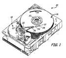
図1は、磁気媒体16のトラック14の上方にスライダ12を位置決めするための駆動システムを含むディスクドライブ10を示す斜視図である。ディスクドライブ10の特定の構成は、説明を容易にするために示されるものであって、いずれも本開示の範囲を限定することを意図していない。ディスクドライブ10は、軸22を中心にスピンドル上でアクチュエータアーム20を回転させるように配置されるボイスコイルモータ18を含む。ロードビーム24は、ヘッドマウントブロック26においてアクチュエータアーム20に接続される。サスペンション28は、ロードビーム24の端部に接続され、スライダ12はサスペンション28に取り付けられる。磁気媒体16は軸30を中心に回転すると、偏流がスライダ12によって生じ、スライダ12が磁気媒体16の表面の上方僅かな距離に維持される。磁気媒体16の各トラック14は、データを記憶するためのデータ記憶セルのアレイによってフォーマットされる。スライダ12は、磁気媒体16のトラック14上においてデータを読み取りおよび/または書き込みするための磁気装置またはトランスデューサ(図1には示されない)を担持する。磁気トランスデューサは、追加の電磁エネルギーを利用して媒体16の表面を加熱し、熱アシスト型磁気記録(HAMR)と称される処理による記録を容易にする。 FIG. 1 is a perspective view showing a disk drive 10 including a drive system for positioning a
HAMRトランスデューサは、磁界を生成して磁気媒体(たとえば磁気媒体16)に書き込みを行うための磁気書き込み部と、書き込み場に近い磁気媒体の部分を加熱するための光学デバイスとを含む。図2は、たとえばHAMR磁気装置40などの磁気装置および関連する磁気記憶媒体42の一部を示す断面図である。HAMR磁気装置40は、台座48によって結合される書き込み磁極44とリターン磁極46とを含む。導体52および54を含むコイル50は、台座を取り巻き、絶縁体56によって支持される。示されるように、磁気記憶媒体42は、硬磁性記憶層62と軟磁性下地層64とを含む垂直磁気媒体であるが、パターンドメディアなどの他の形態の媒体とすることができる。コイルにおける電流は、台座および磁極において磁界を誘発する。磁束58は、空気ベアリング面(ABS)60において記録ヘッドから出て、領域58に囲まれる記憶媒体42の硬磁性層62の部分の磁化を変化させるために使用される。近接場トランスデューサ66は、空気ベアリング面60の近くにおいて書き込み磁極44に隣接して位置決めされる。近接場トランスデューサ66は、レーザなどのエネルギー源から電磁波を受け取る導波路68に結合される。近接場トランスデューサ66の端部における電界は、硬磁性層62の部分69を加熱して保磁力を低下させるために使用され、これによって書き込み磁極からの磁界が記憶媒体の磁化に影響を及ぼすことができる。 The HAMR transducer includes a magnetic writer for generating a magnetic field and writing to a magnetic medium (eg, magnetic medium 16) and an optical device for heating a portion of the magnetic medium near the write field. FIG. 2 is a cross-sectional view illustrating a portion of a magnetic device, such as HAMR magnetic device 40, and associated magnetic storage medium 42, for example. HAMR magnetic device 40 includes a
ここに開示される装置は、他の構造も含み得る。ここに開示される装置は、より大きな装置に組み込まれ得る。たとえば、スライダは、ここに開示されるように装置を含み得る。例示的なスライダは、リーディング端とトレーリング端と空気ベアリング面とを有するスライダ本体を含み得る。そして、書き込み磁極、読み取り磁極、光学近接場トランスデューサ、およびコンタクトパッド(および任意のヒートシンク)は、スライダ本体の上(または中)に位置し得る。このような例示的なスライダは、たとえばディスクドライブに組み込まれ得るサスペンションに取り付けられ得る。なお、開示される装置は、図1に描かれるようなディスクドライブ以外のシステムにおいても利用することができる。 The devices disclosed herein can also include other structures. The devices disclosed herein can be incorporated into larger devices. For example, the slider may include a device as disclosed herein. An exemplary slider may include a slider body having a leading end, a trailing end, and an air bearing surface. The write pole, read pole, optical near field transducer, and contact pad (and optional heat sink) can then be located on (or in) the slider body. Such an example slider may be attached to a suspension that may be incorporated into a disk drive, for example. It should be noted that the disclosed apparatus can be used in systems other than the disk drive as depicted in FIG.
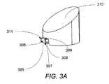
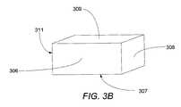
図3Aおよび図3Bは、ペグおよびディスクを有するタイプのNFTにおけるペグおよびディスクの例を示す図であり、図3Bは、図3Aに示されるペグおよびディスクを有するタイプのNFTにおいてペグのみの近接図である。図3AのNFTは、ペグ305とディスク310とを含む。図3Aおよび図3Bに示されるペグ305は、ディスク310に接触しない5つの表面を含み、空気ベアリング面306と、第1の表面307と、第2の表面309と、第3の表面308と、第4の表面311とを含む。 3A and 3B are diagrams showing examples of pegs and disks in a type of NFT having pegs and disks, and FIG. 3B is a close-up view of only pegs in the type of NFT having pegs and disks shown in FIG. 3A. It is. The NFT of FIG. 3A includes a
一部の実施形態において、第2の表面309および第1の表面307は、それぞれ磁極およびコアに面する。一部の実施形態において、第3の表面308および第4の表面311は、磁極またはコアに面していない。より具体的に、第3の表面308は、図2が描かれる紙面の前側に配置され、第4の表面311は、図2が描かれる紙面の後側に配置される。一部の実施形態において、第2の表面309は、NFTポール表面(NFT-pole surface)とも言われ得る。NFTポール表面は、NPS(ここでは示されない)と言われ得るNFTポール空間(NFT-pole space)に面する。一部の実施形態において、第1の表面307は、NFTコア表面とも言われ得る。NFTコア表面は、CNS(ここでは示されない)と言われるNFTコア空間に面する。一部の実施形態において、第3の表面308は、装置の左側に面する表面としても記載され得る。一部の実施形態において、左固浸ミラーがそこに位置し得る。一部の実施形態において、第4の表面311は、装置の右側に面する表面としても記載され得る。一部の実施形態において、右固浸ミラーがそこに位置し得る。 In some embodiments, the
開示される装置は、NFTの1つ以上の表面に位置する1つ以上の相互混合層を含み得る。一部の実施形態において、開示される装置は、NFTのペグの1つ以上の表面上に位置する1つ以上の相互混合層を含み得る。一部の実施形態において、開示される装置は、NFTのペグの2つ以上の表面上に位置する相互混合層を含み得る。一部の実施形態において、開示される装置は、NFTのペグの3つ以上の表面上に位置する相互混合層を含み得る。一部の実施形態において、開示される装置は、NFTのペグの4つ以上の表面上に位置する相互混合層を含み得る。一部の実施形態において、開示される装置は、NFTのペグの全ての5つの表面上に位置する相互混合層を含み得る。一部の実施形態において、開示される装置は、第1の表面307、第2の表面309、第3の表面308、および第4の表面311の各々の上に位置する相互混合層を含み得る。 The disclosed device can include one or more intermixing layers located on one or more surfaces of the NFT. In some embodiments, the disclosed apparatus may include one or more intermixing layers located on one or more surfaces of the NFT pegs. In some embodiments, the disclosed apparatus may include an intermixing layer located on two or more surfaces of the NFT peg. In some embodiments, the disclosed apparatus may include intermixing layers located on more than two surfaces of the NFT peg. In some embodiments, the disclosed apparatus may include intermixing layers located on four or more surfaces of the NFT peg. In some embodiments, the disclosed apparatus may include an intermixing layer located on all five surfaces of the NFT peg. In some embodiments, the disclosed apparatus can include an intermixing layer located on each of the
開示される相互混合層は、様々な特徴を提供するように機能し得る。一部の実施形態において、相互混合層は、(一部の実施形態において)大きく異なる物理的特性、機械的特性、および熱的特性を有する異なる層の接着を向上させるために使用され得る。相互混合層は、その両方に隣接する表面上の層または構造からの材料を含み得る。この隣接する層または構造からの材料の組み合わせにより、物理的特性、機械的特性、および熱的特性の相違が減少し得る。相互混合層を追加することにより、CTEの相違による熱応力を減少させ、結晶構造および格子間隔の相違による界面応力を減少させ、界面エネルギーを減少させることができる。また、相互混合層を追加することにより、界面における欠陥が減少し得る。通常、界面における欠陥は、ペグが凹む際にNFTの原子が拡散するのための重要な通り道である。結果として、相互混合層を追加することにより、ペグの熱的安定性がさらに向上し得る。 The disclosed intermixing layers can function to provide various features. In some embodiments, intermixed layers can be used (in some embodiments) to improve the adhesion of different layers with significantly different physical, mechanical, and thermal properties. The intermixing layer can include material from a layer or structure on the surface adjacent to both. This combination of materials from adjacent layers or structures can reduce differences in physical, mechanical, and thermal properties. By adding the intermixing layer, the thermal stress due to the difference in CTE can be reduced, the interface stress due to the difference in crystal structure and lattice spacing can be reduced, and the interface energy can be reduced. Also, by adding an intermixing layer, defects at the interface can be reduced. Usually, defects at the interface are an important way for the NFT atoms to diffuse as the pegs dent. As a result, the thermal stability of the peg can be further improved by adding an intermixing layer.
開示される相互混合層は、単一の層のみ、または2つ以上の層からなり得る。開示される相互混合層は、他の層と組み合わせて使用され得る。概して、開示される相互混合層は、接着を促すとともに、相互混合層のいずれかの側の構造または層の物理的特性および/または機械的特性の1つ以上の調整を促すように機能する。開示される相互混合層は、下方構造と上方構造との間に位置し得る。一部の実施形態において、相互混合層は、NFTまたはNFTのペグである下方構造と、たとえばCNS、NPS、ヘッドオーバーコート、またはクラッドなどの取り囲む構造である上方構造との間に位置し得る。一部の実施形態において、相互混合層は、NFTまたはNFTのペグである下方構造と、シード層である上方構造との間に位置し得る。一部の実施形態において、相互混合層は、シード層(たとえば、NFTまたはNFTのペグの上に位置決めされるシード層)である下方構造と、たとえばCNS、NPS、ヘッドオーバーコート、またはクラッドなどの上方構造との間に位置し得る。 The disclosed intermixing layers can consist of only a single layer or two or more layers. The disclosed intermixing layers can be used in combination with other layers. In general, the disclosed intermixing layers function to promote adhesion and facilitate one or more adjustments of the physical and / or mechanical properties of the structure or layers on either side of the intermixing layer. The disclosed intermixing layer may be located between the lower structure and the upper structure. In some embodiments, the intermixing layer may be located between a lower structure that is an NFT or NFT peg and an upper structure that is an enclosing structure such as a CNS, NPS, head overcoat, or cladding. In some embodiments, the intermixing layer may be located between a lower structure that is an NFT or NFT peg and an upper structure that is a seed layer. In some embodiments, the intermixing layer includes a lower structure that is a seed layer (eg, a seed layer positioned over a NFT or NFT peg) and a CNS, NPS, head overcoat, or cladding, for example. It may be located between the upper structure.
図4Aは、開示される相互混合層を含む装置の一部を示す断面図である。図4Aは、相互混合層402を示す。また、装置は、下方構造403と上方構造405とを含む。一部の実施形態において、下方構造は、たとえば、NFTまたはより具体的にはNFTのペグを含み得る。一部の実施形態において、下方構造は、たとえば下方のNFTまたはより具体的にはNFTのペグの上に位置決めされるとは限らないシード層を含み得る。一部の実施形態において、上方構造は、取り囲む構造または上方構造を含み得る。例示的な取り囲む構造または上方構造は、たとえば通常は低い屈折率および低い吸収度を有する酸化物、窒化物、またはフッ化物などの誘電材料を含み得る。取り囲む構造または上方構造が作られ得る材料の特定の例示的な材料は、たとえば、SiO、AlO、MgO、B2O3、YO、SrO、CaO、NdO、HoO、ErO、TmO、BeO、ITO、TaO、CrO、NbO、BN、SiN、AlN、LiF、KF、NaF、RbF、MgF2、CaF2、SrF2、BaF2、FeF2、MnF2、NiF2、ZnF2、CdF2、LaF3、PbF2、EuF2、CeF3、PrF3、NdF3、およびTbF3を含み得る。一部の実施形態において、上方構造は、たとえばCNS、NPS、クラッド、ヘッドオーバーコート(HOC)層、またはこれらの組み合わせを含み得る。FIG. 4A is a cross-sectional view illustrating a portion of a device including the disclosed intermixing layer. FIG. 4A shows the intermixing
一部の実施形態において、相互混合層は、少なくとも2つの材料を含み得る。少なくとも2つの材料は、第1の材料と第2の材料とを含み得る。第1の材料は、下方構造403において見出される材料、または下方構造403と相性の良い材料であり得る。下方構造403は、相互混合層の直下において相互混合層に物理的に接触して位置する(または、直下において相互混合層の第1の表面に物理的に接触している)ものとして表され得る。第2の材料は、上方構造405において見出される材料、または上方構造405と相性の良い材料であり得る。他の材料と相性の良い材料は、概して、たとえば比較的高い接着強度を有するなど、2つの材料が比較的良好に互いに接着することや、たとえば同様の熱膨張率(CTE)、同様の格子定数、同様の結晶構造、もしくはこれらの一部を組み合わせた物理的特性および機械的特性における不整合が比較的小さいことなどを意味する。上方構造405は、相互混合層の直上において物理的に接触して位置する(または直下において相互混合層の第2の表面に接触しており、ここで第1の表面は第2の表面の反対側にある)ものとして表され得る。また、開示される相互混合層は、第1の材料と第2の材料とを含むものとして表され得て、第1および第2の材料は、相互混合層に隣接する層または構造と共通している、または相性が良い。 In some embodiments, the intermixing layer can include at least two materials. The at least two materials can include a first material and a second material. The first material can be a material found in the
一部の実施形態において、相互混合層(NFTまたはNFTのペグである下方構造に隣接して位置する)は、第1の材料と第2の材料とを含み得て、ここで第1の材料は下方のNFTにもある材料である。例示的なNFT材料は、たとえば金(Au)、銀(Ag)、アルミニウム(Al)、銅(Cu)、ルテニウム(Ru)、ロジウム(Rh)、イリジウム(Ir)、またはこれらの合金などのプラズモン材料、熱伝導性酸化物、および酸化インジウム錫(ITO)を含み得る。一部の実施形態において、例示的なNFT材料は、米国特許出願公開第2013/0286799号、米国特許第8,427,925号、ならびに 「膜構造を含む磁気装置(MAGNETIC DEVICES INCLUDING FILM STRUCTURES)」と題されて2013年6月21日に出願された米国特許出願第13/923,925号、および「NFTおよびヒートシンクを含む記録ヘッド(RECORDING HEADS INCLUDING NFT AND HEATSINK)」と題されて2013年10月24日に出願された米国特許出願第14/062,651号に開示されるものも含み得て、これらの開示は引用によりここに援用される。一部の実施形態において、相互混合層は、第1の材料として金を含み得る。 In some embodiments, the intermixing layer (located adjacent to a lower structure that is a NFT or NFT peg) can include a first material and a second material, wherein the first material Is a material also in the lower NFT. Exemplary NFT materials include plasmons such as gold (Au), silver (Ag), aluminum (Al), copper (Cu), ruthenium (Ru), rhodium (Rh), iridium (Ir), or alloys thereof. It may include materials, thermally conductive oxides, and indium tin oxide (ITO). In some embodiments, exemplary NFT materials include US 2013/0286799, US Pat. No. 8,427,925, and “MAGNETIC DEVICES INCLUDING FILM STRUCTURES”. US patent application Ser. No. 13 / 923,925 filed Jun. 21, 2013 and “RECORDING HEADS INCLUDING NFT AND HEATSINK”. This may include those disclosed in US patent application Ser. No. 14 / 062,651, filed on Jan. 24, the disclosures of which are hereby incorporated by reference. In some embodiments, the intermixing layer can include gold as the first material.
一部の実施形態において、相互混合層(シード層である下方構造に隣接して位置する)は、第1の材料と第2の材料を含み得て、ここで第1の材料は下方のシード層にもある材料である。例示的なシード層材料は、たとえばレニウム(Re)、タングステン(W)、オスミウム(Os)、イリジウム(Ir)、プラチナ(Pt)、ハフニウム(Hf)、タンタル(Ta)、ルテニウム(Ru)、テクネチウム(Tc)、モリブデン(Mo)、ニオブ(Nb)、ロジウム(Rh)、パラジウム(Pd)、ベリリウム(Be)、クロム(Cr)、シリコン(Si)、ニッケル(Ni)、チタン(Ti)、アルミニウム(Al)、イットリウム(Y)、バナジウム(V)、マグネシウム(Mg)、マンガン(Mn)、コバルト(Co)、またはこれらの組み合わせを含み得る。2つ以上の金属の合金も利用され得る。 In some embodiments, an intermixing layer (located adjacent to a lower structure that is a seed layer) can include a first material and a second material, where the first material is a lower seed. It is also a material in the layer. Exemplary seed layer materials include, for example, rhenium (Re), tungsten (W), osmium (Os), iridium (Ir), platinum (Pt), hafnium (Hf), tantalum (Ta), ruthenium (Ru), technetium. (Tc), molybdenum (Mo), niobium (Nb), rhodium (Rh), palladium (Pd), beryllium (Be), chromium (Cr), silicon (Si), nickel (Ni), titanium (Ti), aluminum (Al), yttrium (Y), vanadium (V), magnesium (Mg), manganese (Mn), cobalt (Co), or combinations thereof. An alloy of two or more metals can also be utilized.
一部の実施形態において、相互混合層は第1の材料と第2の材料とを含み得て、ここで第2の材料は上方構造にもある材料、または上方構造と相性の良い材料である。一部の実施形態において、相互混合層は上方構造としてシード層を有し得る。シード層に含まれ得て、これによって第2の材料として含まれ得る例示的な材料は、たとえばレニウム(Re)、タングステン(W)、オスミウム(Os)、イリジウム(Ir)、プラチナ(Pt)、ハフニウム(Hf)、タンタル(Ta)、ルテニウム(Ru)、テクネチウム(Tc)、モリブデン(Mo)、ニオブ(Nb)、ロジウム(Rh)、パラジウム(Pd)、ベリリウム(Be)、クロム(Cr)、シリコン(Si)、ニッケル(Ni)、チタン(Ti)、アルミニウム(Al)、イットリウム(Y)、バナジウム(V)、マグネシウム(Mg)、マンガン(Mn)、コバルト(Co)、ジルコニウム(Zr)、ネオジム(Nd)、またはこれらの組み合わせを含み得る。2つ以上の金属の合金も利用され得る。 In some embodiments, the intermixing layer can include a first material and a second material, where the second material is a material that is also in the upper structure or a material that is compatible with the upper structure. . In some embodiments, the intermixing layer may have a seed layer as an upper structure. Exemplary materials that can be included in the seed layer and thereby included as the second material include, for example, rhenium (Re), tungsten (W), osmium (Os), iridium (Ir), platinum (Pt), Hafnium (Hf), tantalum (Ta), ruthenium (Ru), technetium (Tc), molybdenum (Mo), niobium (Nb), rhodium (Rh), palladium (Pd), beryllium (Be), chromium (Cr), Silicon (Si), nickel (Ni), titanium (Ti), aluminum (Al), yttrium (Y), vanadium (V), magnesium (Mg), manganese (Mn), cobalt (Co), zirconium (Zr), Neodymium (Nd), or a combination thereof may be included. An alloy of two or more metals can also be utilized.
一部の実施形態において、相互混合層は、第1の材料と第2の材料とを含み得て、ここで第2の材料は上方構造と相性の良い材料である。一部の実施形態において、上方構造と相性の良い材料は、接着層としてよく使用される材料を含み得る。例示的な接着層の材料は、たとえば米国特許出願公開第2014−0004384号、PCT国際出願第US2013/038280号、ならびに、「少なくとも1つの接着層を含む装置(DEVICES INCLUDING AT LEAST ONE ADHESION LAYER)」と題され、米国特許仮出願第61/838,394号の優先権を主張し、Cheng、Zhao、Kautzky、Rejda、Wierman、Franzen、およびBoyneを発明者とし、共通で譲渡されて同時に出願された管理番号430.17840010を有する米国特許出願に開示される材料を含み得て、これらの開示は引用によりここに援用される。 In some embodiments, the intermixing layer can include a first material and a second material, where the second material is a material that is compatible with the upper structure. In some embodiments, the material that is compatible with the superstructure may include a material that is commonly used as an adhesive layer. Exemplary adhesive layer materials include, for example, US Patent Application Publication No. 2014-0004384, PCT International Application No. US2013 / 038280, and “DEVICES INCLUDING AT LEAST ONE ADHESION LAYER”. Claimed the priority of US Provisional Patent Application No. 61 / 838,394, and invented Cheng, Zhao, Kautzky, Rejda, Wierman, Franzen, and Boyne. The materials disclosed in US patent application having control number 430.17840010 may be included, the disclosures of which are hereby incorporated by reference.
一部の実施形態において、相互混合層は、第1の材料と第2の材料とを含み得て、ここで第2の材料は、上方構造と相性の良い材料である。例示的な上方構造のタイプは、CNS、NPS、クラッド、またはヘッドオーバーコートを含み得る。一部の実施形態において、上方構造と相性の良い材料は、たとえば金属、酸化物、窒化物、炭化物、または硫化物を含み得る。CNS、NPS、またはクラッドと相性が良いと考えられ得る例示的な材料は、たとえば容易に酸化される金属、酸化物、および窒化物を含み得る。特定の例示的な金属は、チタン(Ti)、ジルコニウム(Zr)、イリジウム(Ir)、クロム(Cr)、タンタル(Ta)、アルミニウム(Al)、シリコン(Si)、インジウム(In)、マグネシウム(Mg)、ベリリウム(Be)、ハフニウム(Hf)、マンガン(Mn)、ニオブ(Nb)、ホウ素(B)、ニッケル(Ni)、バナジウム(V)、イットリウム(Y)、コバルト(Co)、オスミウム(Os)、およびこれらの組み合わせを含み得る。特定の例示的な酸化物は、たとえば酸化アルミニウム(AlO)、酸化シリコン(SiO)、酸化クロム(CrO)、酸化ニオブ(NbO)、酸化チタン(TiO)、酸化ハフニウム(HfO)、酸化ジルコニウム(ZrO)、酸化タンタル(TaO)、酸化インジウム(InO)、酸化錫(SnO)、酸化インジウム錫(ITO)、酸化マグネシウム(MgO)、酸化イットリウム(YO)、酸化マンガン(MnO)、酸化ストロンチウム(SrO)、およびこれらの組み合わせを含み得る。ここでは2つ以上の非酸素原子を含む酸化物も利用され得る。特定の例示的な窒化物は、たとえば窒化チタン(TiN)、窒化ジルコニウム(ZrN)、窒化クロム(CrN)、窒化ハフニウム(HfN)、窒化ニオブ(NbN)、窒化シリコン(SiN)、窒化アルミニウム(AlN)、窒化ホウ素(BN)、窒化タンタル(TaN)、およびこれらの組み合わせを含み得る。ここでは2つ以上の非窒素原子を含む窒化物も利用され得る。 In some embodiments, the intermixing layer can include a first material and a second material, where the second material is a material that is compatible with the upper structure. Exemplary superstructure types may include CNS, NPS, cladding, or head overcoat. In some embodiments, materials that are compatible with the superstructure may include, for example, metals, oxides, nitrides, carbides, or sulfides. Exemplary materials that may be considered compatible with CNS, NPS, or cladding may include, for example, easily oxidized metals, oxides, and nitrides. Certain exemplary metals include titanium (Ti), zirconium (Zr), iridium (Ir), chromium (Cr), tantalum (Ta), aluminum (Al), silicon (Si), indium (In), magnesium ( Mg), beryllium (Be), hafnium (Hf), manganese (Mn), niobium (Nb), boron (B), nickel (Ni), vanadium (V), yttrium (Y), cobalt (Co), osmium ( Os), and combinations thereof. Specific exemplary oxides include, for example, aluminum oxide (AlO), silicon oxide (SiO), chromium oxide (CrO), niobium oxide (NbO), titanium oxide (TiO), hafnium oxide (HfO), zirconium oxide (ZrO). ), Tantalum oxide (TaO), indium oxide (InO), tin oxide (SnO), indium tin oxide (ITO), magnesium oxide (MgO), yttrium oxide (YO), manganese oxide (MnO), strontium oxide (SrO) , And combinations thereof. Here, oxides containing two or more non-oxygen atoms can also be used. Certain exemplary nitrides include, for example, titanium nitride (TiN), zirconium nitride (ZrN), chromium nitride (CrN), hafnium nitride (HfN), niobium nitride (NbN), silicon nitride (SiN), aluminum nitride (AlN) ), Boron nitride (BN), tantalum nitride (TaN), and combinations thereof. Here, nitrides containing two or more non-nitrogen atoms can also be used.
一部の実施形態において、相互混合層における第2の材料は、金属を含み得て、特定の例示となる金属は、たとえばレニウム(Re)、オスミウム(Os)、イリジウム(Ir)、プラチナ(Pt)、タンタル(Ta)、ルテニウム(Ru)、テクネチウム(Tc)、ロジウム(Rh)、パラジウム(Pd)、ベリリウム(Be)、アルミニウム(Al)、マンガン(Mn)、インジウム(In)、ホウ素(B)、またはこれらの組み合わせを含み得る。一部の実施形態において、金属は、たとえばPt、Ir、Al、Rh、Ru、Pd、またはこれらの組み合わせなどの特定の例示的な金属を含み得る。一部の実施形態において、金属は、たとえばPt、Ir、Al、またはこれらの組み合わせなどの特定の例示的な金属を含み得る。一部の実施形態において、金属は、たとえばPtなどの特定の例示的な金属を含み得る。一部の実施形態において、金属は、たとえばIrなどの特定の例示的な金属を含み得る。一部のこのような実施形態において、金属は、たとえばIr、Pt、Pd、Ru、Rh、Re、Ta、Nb、Os、Al、B、またはこれらの組み合わせなどの特定の例示的な金属を含み得る。2つ以上の金属の合金も利用され得る。 In some embodiments, the second material in the intermixed layer can include a metal, and certain exemplary metals include, for example, rhenium (Re), osmium (Os), iridium (Ir), platinum (Pt ), Tantalum (Ta), ruthenium (Ru), technetium (Tc), rhodium (Rh), palladium (Pd), beryllium (Be), aluminum (Al), manganese (Mn), indium (In), boron (B) ), Or a combination thereof. In some embodiments, the metal may include certain exemplary metals such as, for example, Pt, Ir, Al, Rh, Ru, Pd, or combinations thereof. In some embodiments, the metal can include certain exemplary metals such as, for example, Pt, Ir, Al, or combinations thereof. In some embodiments, the metal may include certain exemplary metals such as, for example, Pt. In some embodiments, the metal may include certain exemplary metals such as Ir. In some such embodiments, the metal includes certain exemplary metals such as, for example, Ir, Pt, Pd, Ru, Rh, Re, Ta, Nb, Os, Al, B, or combinations thereof. obtain. An alloy of two or more metals can also be utilized.
一部の実施形態において、相互混合層における第2の材料は金属を含み得て、特定の例示的な金属は、たとえばタングステン(W)、モリブデン(Mo)、クロム(Cr)、シリコン(Si)、ニッケル(Ni)、チタン(Ti)、イットリウム(Y)、バナジウム(V)、マグネシウム(Mg)、コバルト(Co)、錫(Sn)、ニオブ(Nb)、ハフニウム(Hf)、またはこれらの組み合わせを含み得る。一部の実施形態において、金属は、たとえばCr、Ni、Sn、またはこれらの組み合わせなどの特定の例示的な金属を含み得る。一部の実施形態において、金属は、たとえばCr、Sn、またはこれらの組み合わせなどの特定の例示的な金属を含み得る。一部のこのような実施形態において、金属は、たとえばW、Ti、Cr、Si、Ni、またはこれらの組み合わせなどの特定の例示的な金属を含み得る。2つ以上の金属の合金も利用され得る。 In some embodiments, the second material in the intermixed layer can include a metal, and certain exemplary metals include, for example, tungsten (W), molybdenum (Mo), chromium (Cr), silicon (Si). , Nickel (Ni), titanium (Ti), yttrium (Y), vanadium (V), magnesium (Mg), cobalt (Co), tin (Sn), niobium (Nb), hafnium (Hf), or a combination thereof Can be included. In some embodiments, the metal may include certain exemplary metals such as, for example, Cr, Ni, Sn, or combinations thereof. In some embodiments, the metal can include certain exemplary metals such as, for example, Cr, Sn, or combinations thereof. In some such embodiments, the metal may include certain exemplary metals such as, for example, W, Ti, Cr, Si, Ni, or combinations thereof. An alloy of two or more metals can also be utilized.
一部の実施形態において、相互混合層における第2の材料は金属を含み得て、特定の例示的な金属は、たとえばRe、Os、Ir、Pt、Hf、Ta、Ru、Tc、Nb、Rh、Pd、Be、Al、Mn、In、W、Mo、Cr、Si、Ni、Ti、Zr、Y、V、Mg、Co、Sn、またはこれらの組み合わせを含み得る。一部のこのような実施形態において、金属は、たとえばIr、Pt、Pd、Nb、Ru、Re、Ta、Os、Al、B、W、Ti、Cr、Si、Ni、またはこれらの組み合わせなどの特定の例示的な金属を含み得る。一部の実施形態において、金属は、たとえばPt、Ir、Al、Cr、Ni、Sn、またはこれらの組み合わせなどの特定の例示的な金属を含み得る。一部の実施形態において、金属は、たとえばPt、Ir、Cr、Sn、またはこれらの一部の組み合わせなどの特定の例示的な金属を含み得る。一部の実施形態において、金属は、NFTの使用時において接着層が酸化しないように、酸化に対して比較的高い耐性を有する金属を含み得る。一部のこのような実施形態において、金属は、たとえばIr、Pt、Pd、Nb、Ru、Re、Ta、Nb、Os、Al、B、W、Ti、Cr、Si、Ni、またはこれらの組み合わせなどの特定の例示的な金属を含み得る。2つ以上の金属の合金も利用され得る。 In some embodiments, the second material in the intermixed layer can include a metal, and certain exemplary metals include, for example, Re, Os, Ir, Pt, Hf, Ta, Ru, Tc, Nb, Rh. , Pd, Be, Al, Mn, In, W, Mo, Cr, Si, Ni, Ti, Zr, Y, V, Mg, Co, Sn, or combinations thereof. In some such embodiments, the metal is, for example, Ir, Pt, Pd, Nb, Ru, Re, Ta, Os, Al, B, W, Ti, Cr, Si, Ni, or combinations thereof Certain exemplary metals may be included. In some embodiments, the metal can include certain exemplary metals such as, for example, Pt, Ir, Al, Cr, Ni, Sn, or combinations thereof. In some embodiments, the metal can include certain exemplary metals such as, for example, Pt, Ir, Cr, Sn, or some combination thereof. In some embodiments, the metal may include a metal that has a relatively high resistance to oxidation so that the adhesion layer does not oxidize when using NFT. In some such embodiments, the metal is, for example, Ir, Pt, Pd, Nb, Ru, Re, Ta, Nb, Os, Al, B, W, Ti, Cr, Si, Ni, or combinations thereof May include certain exemplary metals. An alloy of two or more metals can also be utilized.
一部の実施形態において、相互混合層における第2の材料は金属を含み得て、特定の例示的な金属は、たとえばジルコニウム(Zr)、チタン(Ti)、イットリウム(Y)、スカンジウム(Sc)、アルミニウム(Al)、ルテニウム(Ru)、バナジウム(V)、シリコン(Si)、ゲルマニウム(Ge)、タンタル(Ta)、および錫(Sn)を含み得る。一部の実施形態において、相互混合層における第2の材料は金属を含み得て、特定の例示的な金属は、たとえばコバルト(Co)、ニッケル(Ni)、クロム(Cr)、タングステン(W)、チタン・タングステン(TiW)、モリブデン(Mo)、マグネシウム(Mg)、ニオブ(Nb)、ハフニウム(Hf)、亜鉛(Zn)、またはこれらの一部の組み合わせを含み得る。2つ以上の金属の合金も利用され得る。 In some embodiments, the second material in the intermixed layer can include a metal, and certain exemplary metals include, for example, zirconium (Zr), titanium (Ti), yttrium (Y), scandium (Sc). , Aluminum (Al), ruthenium (Ru), vanadium (V), silicon (Si), germanium (Ge), tantalum (Ta), and tin (Sn). In some embodiments, the second material in the intermixed layer can include a metal, and certain exemplary metals include, for example, cobalt (Co), nickel (Ni), chromium (Cr), tungsten (W). , Titanium-tungsten (TiW), molybdenum (Mo), magnesium (Mg), niobium (Nb), hafnium (Hf), zinc (Zn), or some combination thereof. An alloy of two or more metals can also be utilized.
特定の例示的な相互混合層は、第1の材料として金を含有し、第2の材料として金属を含有し得る。このため、このような相互混合層は、金相(gold phase)を有する金合金、または金属間相(intermetallic phase)を有する金合金として特徴付けられ得る。このような相互混合層は、事実上の金のガスバリア層によって金における他の元素(不純物)の耐酸化性が高まり得る。このような相互混合層は、上方層と下方層との間における物理的特性、機械的特性、熱的特性、またはこれらの一部の組み合わせの不整合を減少させ、界面エネルギーも減少させ得る。 Certain exemplary intermixed layers may contain gold as the first material and metal as the second material. Thus, such intermixed layers can be characterized as gold alloys having a gold phase or gold alloys having an intermetallic phase. Such an intermixing layer can increase the oxidation resistance of other elements (impurities) in the gold by the effective gold gas barrier layer. Such intermixing layers can reduce the mismatch of physical properties, mechanical properties, thermal properties, or some combination thereof between the upper and lower layers, and can also reduce the interfacial energy.
一部の実施形態において、相互混合層における第2の材料は、窒化物を含み得て、特定の例示的な窒化物は、たとえば窒化クロム(CrN)、窒化ホウ素(BN)、窒化ニオブ(NbN)、窒化シリコン(SiN)、窒化アルミニウム(AlN)、またはこれらの一部の組み合わせを含み得る。一部の実施形態において、相互混合層における第2の材料は、窒化物を含み得て、特定の例示的な窒化物は、たとえば窒化チタン(TiN)、窒化ジルコニウム(ZrN)、窒化タンタル(TaN)、窒化ハフニウム(HfN)、またはこれらの一部の組み合わせを含み得る。ここでは2つ以上の窒素原子を含む窒化物が使用され得る。 In some embodiments, the second material in the intermixed layer can include nitride, and certain exemplary nitrides include, for example, chromium nitride (CrN), boron nitride (BN), niobium nitride (NbN). ), Silicon nitride (SiN), aluminum nitride (AlN), or some combination thereof. In some embodiments, the second material in the intermixed layer can include nitride, and certain exemplary nitrides can be, for example, titanium nitride (TiN), zirconium nitride (ZrN), tantalum nitride (TaN). ), Hafnium nitride (HfN), or some combination thereof. Here, nitrides containing two or more nitrogen atoms can be used.
一部の実施形態において、相互混合層における第2の材料は酸化物を含み得て、特定の例示的な酸化物は、たとえば酸化アルミニウム(AlO)、酸化イットリウム(YO)、酸化インジウム(In2O3)、酸化錫(SnO2)、酸化亜鉛(ZnO)(たとえば、ドープしたZnO、たとえばアルミニウム(Al)でドープしたZnO、またはガリウム(Ga)でドープしたZnO)、酸化ベリリウム(BeO)、酸化シリコン(SiO)、酸化鉄(FeO)、酸化チタン(TiO)、酸化ジルコニウム(ZrO)、酸化タンタル(TaO)、酸化マンガン(MnO)、酸化カドミウム(CdO)、酸化マグネシウム(MgO)、酸化ハフニウム(HfO)、酸化クロム(CrO)、酸化ストロンチウム(SrO)、酸化ニオブ(NbO)、またはこれらの一部の組み合わせを含み得る。一部の実施形態において、酸化物は、たとえば酸化錫(SnO)、酸化インジウム(InO)、またはこれらの一部の組み合わせなどの特定の例示的な酸化物を含み得る。一部の実施形態において、酸化物は、たとえば酸化ベリリウム(BeO)、酸化シリコン(SiO)、酸化鉄(FeO)、酸化アルミニウム(AlO)、酸化チタン(TiO)、酸化ジルコニウム(ZrO)、酸化タンタル(TaO)、酸化マンガン(MnO)、酸化カドミウム(CdO)、酸化錫(SnO)、酸化インジウム(InO)、酸化インジウム錫(ITO)、またはこれらの一部の組み合わせなどの特定の例示的な酸化物を含み得る。なお、酸化物は、特定的に記載された元素および酸素を含む任意の化学量を含み得る。たとえば酸化シリコンは、二酸化シリコン(SiO2)および一酸化シリコン(SiO)の両方を含む。2つ以上の非酸素原子を含む酸化物もここで使用され得て、たとえばIn2O3−SnO2(ITO)(たとえば、固溶体)、TaSiO、AlSiO、およびYAlOが含まれ得る。In some embodiments, the second material in the intermixed layer can include an oxide, and certain exemplary oxides include, for example, aluminum oxide (AlO), yttrium oxide (YO), indium oxide (In2 ). O3 ), tin oxide (SnO2 ), zinc oxide (ZnO) (eg doped ZnO, eg ZnO doped with aluminum (Al) or ZnO doped with gallium (Ga)), beryllium oxide (BeO), Silicon oxide (SiO), iron oxide (FeO), titanium oxide (TiO), zirconium oxide (ZrO), tantalum oxide (TaO), manganese oxide (MnO), cadmium oxide (CdO), magnesium oxide (MgO), hafnium oxide (HfO), chromium oxide (CrO), strontium oxide (SrO), niobium oxide (Nb) ), Or a combination of some of these. In some embodiments, the oxide may include certain exemplary oxides such as, for example, tin oxide (SnO), indium oxide (InO), or some combination thereof. In some embodiments, the oxide is, for example, beryllium oxide (BeO), silicon oxide (SiO), iron oxide (FeO), aluminum oxide (AlO), titanium oxide (TiO), zirconium oxide (ZrO), tantalum oxide. Certain exemplary oxidations such as (TaO), manganese oxide (MnO), cadmium oxide (CdO), tin oxide (SnO), indium oxide (InO), indium tin oxide (ITO), or some combination thereof Can contain things. It should be noted that the oxide can include any stoichiometry including the specifically described elements and oxygen. For example, silicon oxide includes both silicon dioxide (SiO2 ) and silicon monoxide (SiO). Oxides containing two or more non-oxygen atoms can also be used here and can include, for example, In2 O3 —SnO2 (ITO) (eg, solid solution), TaSiO, AlSiO, and YAlO.
一部の実施形態において、相互混合層における第2の材料は炭化物を含み得て、特定の例示的な炭化物は、たとえば炭化タンタル(TaC)、炭化ウラン(UC)、炭化ハフニウム(HfC)、炭化ジルコニウム(ZrC)、炭化スカンジウム(ScC)、炭化マンガン(MnC)、炭化鉄(FeC)、炭化ニオブ(NbC)、炭化テクネチウム(TcC)、炭化レニウム(ReC)、またはこれらの一部の組み合わせを含み得る。一部の実施形態において、炭化物は、たとえば炭化バナジウム(VC)、炭化タングステン(WC)、炭化チタン(TiC)、炭化クロム(CrC)、炭化コバルト(CoC)、炭化ニッケル(NiC)、炭化イットリウム(YC)、炭化モリブデン(MoC)、またはこれらの一部の組み合わせなどの特定の例示的な炭化物を含み得る。一部の実施形態において、炭化物は、たとえば炭化バナジウム(VC)、炭化タンタル(TaC)、炭化チタン(TiC)、炭化ウラン(UC)、炭化タングステン(WC)、炭化ハフニウム(HfC)、炭化ジルコニウム(ZrC)、炭化クロム(CrC)、炭化スカンジウム(ScC)、炭化マンガン(MnC)、炭化鉄(FeC)、炭化コバルト(CoC)、炭化ニッケル(NiC)、炭化イットリウム(YC)、炭化ニオブ(NbC)、炭化モリブデン(MoC)、炭化テクネチウム(TcC)、炭化レニウム(ReC)、またはこれらの一部の組み合わせなどの特定の例示的な炭化物を含み得る。一部の実施形態において、相互混合層における第2の材料は炭化物を含み得て、特定の例示的な炭化物は、たとえば炭化シリコン(SiC)、水素化炭化シリコン(SiC:H)、またはこれらの組み合わせを含み得る。ここでは2つ以上の炭素原子を含む炭化物も利用され得る。 In some embodiments, the second material in the intermixed layer can include carbides, and certain exemplary carbides include, for example, tantalum carbide (TaC), uranium carbide (UC), hafnium carbide (HfC), carbonization. Including zirconium (ZrC), scandium carbide (ScC), manganese carbide (MnC), iron carbide (FeC), niobium carbide (NbC), technetium carbide (TcC), rhenium carbide (ReC), or some combination thereof obtain. In some embodiments, the carbide is, for example, vanadium carbide (VC), tungsten carbide (WC), titanium carbide (TiC), chromium carbide (CrC), cobalt carbide (CoC), nickel carbide (NiC), yttrium carbide ( Specific exemplary carbides such as YC), molybdenum carbide (MoC), or some combination thereof. In some embodiments, the carbide is, for example, vanadium carbide (VC), tantalum carbide (TaC), titanium carbide (TiC), uranium carbide (UC), tungsten carbide (WC), hafnium carbide (HfC), zirconium carbide ( ZrC), chromium carbide (CrC), scandium carbide (ScC), manganese carbide (MnC), iron carbide (FeC), cobalt carbide (CoC), nickel carbide (NiC), yttrium carbide (YC), niobium carbide (NbC) , Specific carbides such as molybdenum carbide (MoC), technetium carbide (TcC), rhenium carbide (ReC), or some combination thereof. In some embodiments, the second material in the intermixed layer can include carbides, and certain exemplary carbides are, for example, silicon carbide (SiC), hydrogenated silicon carbide (SiC: H), or these Combinations can be included. Carbides containing two or more carbon atoms can also be used here.
一部の実施形態において、相互混合層における第2の材料は硫化物を含み得て、特定の例示的な硫化物は、たとえば硫化ジルコニウム、硫化亜鉛、硫化チタン、硫化コバルト、硫化銀、硫化銅、硫化インジウム、硫化カドミウム、硫化錫、硫化ビスマス、硫化鉛、硫化セレニウム、硫化鉄、 硫化モリブデン、 およびこれらの組み合わせを含み得る。なお、硫化物は、特定的に記載された元素および硫黄を含む化学量を含み得る。ここでは2つ以上の硫黄原子を含む硫化物も利用され得る。 In some embodiments, the second material in the intermixed layer can include sulfide, and certain exemplary sulfides include, for example, zirconium sulfide, zinc sulfide, titanium sulfide, cobalt sulfide, silver sulfide, copper sulfide. , Indium sulfide, cadmium sulfide, tin sulfide, bismuth sulfide, lead sulfide, selenium sulfide, iron sulfide, molybdenum sulfide, and combinations thereof. It should be noted that the sulfide may include a stoichiometric amount that includes specifically described elements and sulfur. Sulfides containing two or more sulfur atoms can also be used here.
特定の例示的な相互混合層は、第1の材料として金を含み得て、第2の材料として窒化物、酸化物、炭化物、または硫化物を含み得る。このため、このような相互混合層は、相互混合層に金原子を含み、金原子クラスタまたは金ナノ粒子を形成し得るものとして特徴づけられる。このような金ナノ粒子は、増大された表面接触領域および機械的連結によって、金と酸化物、窒化物、炭化物、または硫化物の接着層との間の接着を大きく向上させる。 Certain exemplary intermixed layers can include gold as the first material and nitride, oxide, carbide, or sulfide as the second material. For this reason, such an intermixed layer is characterized in that it can contain gold atoms in the intermixed layer to form gold atom clusters or gold nanoparticles. Such gold nanoparticles greatly improve the adhesion between gold and oxide, nitride, carbide, or sulfide adhesion layers due to increased surface contact area and mechanical coupling.
開示される相互混合層は、一部の実施形態において少なくとも0.1nm(1Å)の厚さを有し得る、一部の実施形態において少なくとも0.2nm(2Å)の厚さを有し得る、または一部の実施形態において少なくとも1nm(10Å)の厚さを有し得る。開示される相互混合層は、一部の実施形態において100nm(1000Å)以下の厚さを有し得る、一部の実施形態において40nm(400Å)以下の厚さを有し得る、一部の実施形態において5nm(50Å)以下の厚さを有し得る、または一部の実施形態において3.5nm(35Å)以下の厚さを有し得る。相互混合層の厚さ(たとえば、平均厚さ)は、たとえば透過型電子顕微鏡 (TEM)、X線反射率(XRR)、またはX線光電子分光法 (XPS)を用いて測定され得る。たとえば、厚さは既知の厚さを有する標準サンプルからの較正を用いて判定され得る。 The disclosed intermixed layers can have a thickness of at least 0.1 nm (1 Å) in some embodiments, and can have a thickness of at least 0.2 nm (2 Å) in some embodiments. Or, in some embodiments, it may have a thickness of at least 1 nm (10 cm). The disclosed intermixed layers may have a thickness of 100 nm (1000 Å) or less in some embodiments, and may have a thickness of 40 nm (400 Å) or less in some embodiments. The form may have a thickness of 5 nm (50 以下) or less, or in some embodiments may have a thickness of 3.5 nm (35 Å) or less. The thickness (eg, average thickness) of the intermixing layer can be measured using, for example, transmission electron microscopy (TEM), X-ray reflectivity (XRR), or X-ray photoelectron spectroscopy (XPS). For example, the thickness can be determined using calibration from a standard sample having a known thickness.
第1の材料と第2の材料とを含む開示される相互混合層は、相互混合層にわたって単一の実質的に均質な組成を有する単層であり得る。一部の実施形態において、開示される相互混合層は、相互混合層の全体にわたって実質的に均質でない組成を有し得る。たとえば、一部の実施形態において、開示される相互混合層は、一方の表面から他方の表面へ変化する組成を有し得る、または組成勾配を有し得る。たとえば、開示される相互混合層は、一方の表面から他方の表面へ変化する第1の材料(または第2の材料)の量を有し得る。より具体的には、開示される相互混合層は、第1の表面から第2の表面(第2の表面は第1の表面の反対側)へ変化する第1の材料の量を有し得る。例示的な例は、(たとえば)NFTと物理的に接触する第1の表面から(たとえば)接着層と物理的に接触する第2の表面へ変化する第1の材料の量を有する相互混合層を含み得る。他の特定の例示的な例は、NFTと物理的に接触する第1の表面から接着層と物理的に接触する第2の表面へ変化する金の量を有する相互混合層を含む。他の特定の例示的な例は、NFTと物理的に接触する第1の表面におけるほぼ100%の金から接着層と接触する第2の表面におけるほぼ100%の第2の材料へ変化する組成を有する相互混合層を含む。 The disclosed intermixing layer comprising the first material and the second material can be a single layer having a single substantially homogeneous composition across the intermixing layer. In some embodiments, the disclosed intermixing layer can have a substantially non-homogeneous composition throughout the intermixing layer. For example, in some embodiments, the disclosed intermixing layer can have a composition that varies from one surface to the other, or can have a composition gradient. For example, the disclosed intermixing layer can have an amount of a first material (or second material) that varies from one surface to the other. More specifically, the disclosed intermixing layer can have an amount of a first material that varies from a first surface to a second surface (the second surface is opposite the first surface). . An illustrative example is an intermixed layer having an amount of a first material that varies from a first surface in physical contact with (for example) NFT to a second surface in physical contact with (for example) an adhesive layer. Can be included. Another specific illustrative example includes an intermixing layer having an amount of gold that varies from a first surface in physical contact with the NFT to a second surface in physical contact with the adhesive layer. Another specific illustrative example is a composition that varies from approximately 100% gold on the first surface in physical contact with the NFT to approximately 100% second material on the second surface in contact with the adhesive layer. Including an intermixing layer.
開示される相互混合層、たとえば第1の材料と第2の材料とを含有する相互混合層は、様々なプロセスを用いて形成され得る。一部の実施形態において、第1の材料と第2の材料とを含有する開示される相互混合層は、第1の材料と第2の材料との共堆積によって形成され得る。たとえば、開示される相互混合層は、NFT材料もしくはシード層材料と接着層材料との共堆積によって形成され得る。たとえば、開示される相互混合層は、金と金属、酸化物、窒化物、炭化物、もしくは硫化物との共堆積によって形成され得る。一部の実施形態において、相互混合層は、必ずしも異なる組成を有さず、必ずしも同じでない組成勾配を必ずしも有さない複数の相互混合層を含み得る。一部の実施形態において、相互混合層は、(第1の材料を含み得る)下方構造との界面から(第2の材料を含み得る)上方構造との界面に向かうにつれて層にわたって第2の材料の濃度が高まるような組成を有し得る。 The disclosed intermixing layers, such as intermixing layers containing a first material and a second material, can be formed using a variety of processes. In some embodiments, the disclosed intermixed layer containing the first material and the second material can be formed by co-deposition of the first material and the second material. For example, the disclosed intermixing layer can be formed by co-deposition of NFT material or seed layer material and adhesive layer material. For example, the disclosed intermixed layers can be formed by co-deposition of gold and metal, oxide, nitride, carbide, or sulfide. In some embodiments, the intermixing layer may include a plurality of intermixing layers that do not necessarily have different compositions and do not necessarily have different composition gradients. In some embodiments, the intermixing layer includes a second material across the layer from the interface with the lower structure (which may include the first material) toward the interface with the upper structure (which may include the second material). The composition may have a concentration that increases.
一部の実施形態において、相互混合層は、第1および第2の材料の層を交互に堆積させることによっても形成され得る。第1および第2の材料の層厚さは、所望の濃度を有する相互混合層を作るために異なり得る。一部の実施形態において、第1の材料と第2の材料とが交互に設けられた層からなる相互混合層は、(第1の材料を含み得る)下方構造との界面から(第2の材料を含み得る)上方構造との界面に向かうにつれて層にわたって第2の材料の濃度が高まるような組成を有し得て、このような実施形態において、これは2つの層の厚さを変えることによって達成され得る。 In some embodiments, the intermixing layer can also be formed by alternately depositing layers of first and second materials. The layer thicknesses of the first and second materials can be different to produce an intermixed layer having a desired concentration. In some embodiments, the intermixed layer comprising alternating layers of the first material and the second material is from the interface with the underlying structure (which may include the first material) (the second material). It may have a composition that increases the concentration of the second material across the layer as it goes to the interface with the superstructure), and in such embodiments this will change the thickness of the two layers Can be achieved.
第1の材料と第2の材料とを含有する開示される相互混合層は、電気化学法、物理蒸着法、化学蒸着法、またはこれらの様々な組み合わせによっても形成され得る。第1の材料と第2の材料とを含有する開示される相互混合層は、イオン注入、高温堆積、高バイアス堆積、熱アニール、レーザ照射、電子ビーム照射、またはこれらの様々な組み合わせを用いても形成され得る。 The disclosed intermixed layers containing the first material and the second material can also be formed by electrochemical methods, physical vapor deposition methods, chemical vapor deposition methods, or various combinations thereof. The disclosed intermixed layer containing the first material and the second material can be obtained using ion implantation, high temperature deposition, high bias deposition, thermal annealing, laser irradiation, electron beam irradiation, or various combinations thereof. Can also be formed.
開示される相互混合層は、隣接する層または構造と共通の第1の材料と第2の材料とを含む相互混合層を堆積させ、NFTと物理的に接触していない相互混合層の表面を酸化させることによっても形成され得る。このような相互混合層は、図4Bに描かれる。相互混合層412の上部表面を酸化させるステップは、そこに酸化層414を形成するよう機能し得て、これによって、相互混合層の光学的性質が向上する、相互混合層の熱的安定性が向上する、隣接する構造との接着が向上する、またはこれらの組み合わせが得られる。一部の例示的な実施形態において、このような相互混合層は、イオン注入、高温堆積、高バイアス堆積、または熱アニール後の堆積によって堆積され得て、これによってNFTペグに対する相互混合層の接着が向上する。そして、相互混合層412の上部表面がプラズマ酸化、空気酸化、オゾン酸化、または熱酸化を用いて酸化され得て、たとえば上方構造405への相互混合層の接着を向上させ得る酸化層414が形成される。 The disclosed intermixing layer deposits an intermixing layer that includes a first material and a second material that are common to adjacent layers or structures, and provides a surface of the intermixing layer that is not in physical contact with the NFT. It can also be formed by oxidation. Such an intermixing layer is depicted in FIG. 4B. The step of oxidizing the top surface of the intermixing layer 412 may function to form an
一部の特定的な実施形態において、NFTに隣接する相互混合層は、NFTと少なくとも二次的な元素を含有する合金を含み得る。このような相互混合層は、合金相互混合層と呼ばれるが、必ずしもこう呼ぶ必要はない。このような合金相互混合層は、NFT材料(たとえば金)の優れた光学的性質およびNFT材料を含む合金の比較的高い熱的安定性の利点を生かし得る。このようなことから、これらのタイプの合金相互混合層は、NFTまたはペグ全体がもっぱら合金からなるよりも有利となり得る。また、このような合金相互混合層は、ペグが合金からなる場合に利用され得る。このような場合において、合金相互混合層は、ペグの合金よりも二次的な元素の含有量が高くなり得る。なぜなら、合金相互混合層の厚さが比較的小さいことにより高い光学ペナルティがなくなるからである。また、二次的な元素がペグおよび合金相互混合層において同じである場合において、システムは両構造が同じ結晶構造を有することから利益を得ることができる。これは、界面が非常に低い界面エネルギーを有し、これによって界面拡散が減少することを意味する。 In some specific embodiments, the intermixing layer adjacent to the NFT may include an alloy containing NFT and at least a secondary element. Such an intermixing layer is called an alloy intermixing layer, but it is not always necessary to call it this way. Such alloy intermixing layers can take advantage of the superior optical properties of NFT materials (eg, gold) and the relatively high thermal stability of alloys containing NFT materials. As such, these types of alloy intermixed layers can be advantageous over the entire NFT or peg consisting entirely of alloys. Such an alloy intermixing layer can be used when the peg is made of an alloy. In such a case, the alloy intermixing layer can have a higher secondary element content than the peg alloy. This is because the high optical penalty is eliminated by the relatively small thickness of the alloy intermixing layer. Also, if the secondary elements are the same in the peg and alloy intermixed layers, the system can benefit from both structures having the same crystal structure. This means that the interface has a very low interfacial energy, which reduces interfacial diffusion.
このような合金相互混合層は、NFTの全ての表面上に、またはNFTの全ての表面よりも少ない表面上に含まれ得る。一部の実施形態において、このような合金相互混合層は、ペグおよびディスクを有するタイプのNFTの全ての表面上に含まれ得る。一部の実施形態において、このような合金相互混合層は、ABS以外のペグの全ての表面上に含まれ得る。図3Aおよび図3Bを再び参照すると、このような合金相互混合層は、たとえば、図3Aおよび図3Bに示される第1の表面307、第2の表面309、第3の表面308、および第4の表面311の上に含まれ得る。図5Aは、ABSから見たペグ505を示し、合金相互混合層502が全ての4つの表面に設けられる。そこに見られるように、合金相互混合層502は、ペグの全ての4つの表面上に位置する単一の連続した層として描かれる。なお、4つの表面上の合金相互混合層は、分離して設けられ得る、隣接する相互混合層に対して不連続であり得る、またはこれらの一部の組み合わせであり得る。 Such an alloy intermixing layer can be included on all surfaces of the NFT or on less than all surfaces of the NFT. In some embodiments, such alloy intermixing layers can be included on all surfaces of a type of NFT having pegs and disks. In some embodiments, such an alloy intermixing layer can be included on all surfaces of the peg other than ABS. Referring again to FIGS. 3A and 3B, such alloy intermixing layers include, for example, the
このような例示的な合金相互混合層を構成する合金は、NFT材料/X合金と言われ得る。一部の実施形態において、NFTは金または金合金からなり得る。このような実施形態において、合金相互混合層の合金は、AuXとして付与され得る。Xは、たとえばコバルト(Co)、ニッケル(Ni)、クロム(Cr)、プラチナ(Pt)、ホウ素(B)、鉄(Fe)、アルミニウム(Al)、タンタル(Ta)、タングステン(W)、シリコン(Si)、チタン(Ti)、イリジウム(Ir)、ジルコニウム(Zr)、またはこれらの一部の組み合わせを含み得る。一部の実施形態において、合金相互混合層は、三元合金を含み得る。一部の実施形態において、たとえばNFTは金からなり得て、合金相互混合層は金コバルト合金からなり得る。 The alloy making up such an exemplary alloy intermixing layer may be referred to as an NFT material / X alloy. In some embodiments, the NFT can consist of gold or a gold alloy. In such an embodiment, the alloy of the alloy intermixing layer may be applied as AuX. X is, for example, cobalt (Co), nickel (Ni), chromium (Cr), platinum (Pt), boron (B), iron (Fe), aluminum (Al), tantalum (Ta), tungsten (W), silicon (Si), titanium (Ti), iridium (Ir), zirconium (Zr), or some combination thereof. In some embodiments, the alloy intermixing layer can include a ternary alloy. In some embodiments, for example, the NFT can be made of gold and the alloy intermixing layer can be made of a gold-cobalt alloy.
合金相互混合層の合金は、様々な量の二次的な元素を有し得る。合金相互混合層の合金は、一部の実施形態において0.1原子%(原子パーセント)以上の二次的な元素(X)を有し得る、または一部の実施形態において5原子%以上を有し得る。合金相互混合層の合金は、一部の実施形態において90原子%以下の二次的な元素(X)を有し得る、または一部の実施形態において50原子%以下を有し得る。 The alloy of the alloy intermixing layer can have various amounts of secondary elements. The alloy of the alloy intermixed layer may have a secondary element (X) of 0.1 atomic% (atomic percent) or more in some embodiments, or 5 atomic% or more in some embodiments. Can have. The alloy of the alloy intermixed layer may have 90 atomic percent or less secondary element (X) in some embodiments, or may have 50 atomic percent or less in some embodiments.
開示される合金相互混合層は、一部の実施形態において少なくとも0.1nm(1Å)の厚さを有し得る、または一部の実施形態において少なくとも1nm(10Å)の厚さを有し得る。開示される合金相互混合層は、一部の実施形態において40nm(400Å)以下の厚さを有し得る、または一部の実施形態において15nm(150Å)以下の厚さを有し得る。合金相互混合層の厚さ(たとえば、平均厚さ)は、たとえば、透過型電子顕微鏡(TEM)、X線反射率(XRR)、またはX線光電子分光法(XPS)を用いて測定され得る。たとえば、厚さは既知の厚さを有する標準サンプルからの較正を用いて判定され得る。 The disclosed alloy intermixing layers can have a thickness of at least 0.1 nm (1 Å) in some embodiments, or can have a thickness of at least 1 nm (10 Å) in some embodiments. The disclosed alloy intermixed layers may have a thickness of 40 nm (400 Å) or less in some embodiments, or may have a thickness of 15 nm (150 Å) or less in some embodiments. The thickness (eg, average thickness) of the alloy intermixing layer can be measured using, for example, transmission electron microscopy (TEM), X-ray reflectivity (XRR), or X-ray photoelectron spectroscopy (XPS). For example, the thickness can be determined using calibration from a standard sample having a known thickness.
一部の特定的な実施形態において、シード層に隣接する相互混合層は、シード層材料と少なくとも二次的な元素とを含有する合金を含み得る。このような実施形態は、ここで下方構造403がペグであって上方構造405がシード層である図4Aに描かれる実施形態と同様となり得る。図5Bは、ペグ505を示し、ペグ505は、その上に合金相互混合層502を有し、合金相互混合層502の上にシード層506を有する。シード層506は、たとえばオーバーコート層などのシード層506の上に形成される層の堆積を補助したり、たとえばオーバーコート層などのシード層506の上に形成される層の特性を調整するために利用され得る。シード層の材料は、シード層の後に堆積される材料に少なくとも一部が依存する(たとえば、オーバーコート層の材料、またはCNS、NPS、クラッド、またはこれらの組み合わせ)。一部の実施形態において、シード層は金属を含み得る。一部の実施形態において、例示的な金属は、たとえばクロム(Cr)、ニッケル(Ni)、コバルト(Co)、タングステン(W)、チタン(Ti)、プラチナ(Pt)、イリジウム(Ir)、タンタル(Ta)、ジルコニウム(Zr)、モリブデン(Mo)、ロジウム(Rh)、ルテニウム(Ru)、ニオブ(Nb)、イットリウム(Y)、パラジウム(Pd)、またはこれらの一部の組み合わせを含み得る。一部の実施形態において、例示的な金属は、たとえばCrを含み得る。シード層は、様々な厚さを有し得る。シード層は、一部の実施形態において少なくとも0.05nm(0.5Å)の厚さを有し得る、または一部の実施形態において少なくとも0.5nm(5Å)の厚さを有し得る。シード層は、一部の実施形態において40nm(400Å)以下の厚さを有し得て、一部の実施形態において5nm(50Å)以下の厚さを有し得る。 In some specific embodiments, the intermixed layer adjacent to the seed layer can include an alloy containing a seed layer material and at least a secondary element. Such an embodiment may be similar to the embodiment depicted in FIG. 4A where the
開示される合金相互混合層および任意のシード層の利用は、取り囲む材料とのペグ(たとえば、金からなる)の界面エネルギーを減少させるよう機能し、ペグの熱的安定性が高まる。 The use of the disclosed alloy intermixing layer and optional seed layer serves to reduce the interfacial energy of the peg (eg, composed of gold) with the surrounding material, increasing the thermal stability of the peg.
一部の実施形態において、合金相互混合層は、NFTのペグのみでなくそれ以外にも配置され得る。たとえば、相互混合層(合金相互混合層またはその他)は、ロッド全体における1つ以上の表面上に配置され得る。ロッドは、概してペグの後部として表される(ペグのABSから離れる方向)。代替的に、ロッドは、ペグがロッドの一部である点において、ロッドが形成されるプロセスによって表され得て、ペグはロッドのみの前部(ABSに向けて)として表される。一部の実施形態において、ロッドはペグであり得る。 In some embodiments, the alloy intermixing layer may be disposed in addition to NFT pegs. For example, an intermixing layer (alloy intermixing layer or otherwise) can be disposed on one or more surfaces in the entire rod. The rod is generally represented as the back of the peg (in the direction away from the peg's ABS). Alternatively, the rod can be represented by the process by which the rod is formed in that the peg is part of the rod, the peg being represented as the front of the rod only (towards the ABS). In some embodiments, the rod can be a peg.
図6Aは、ペグ602、ディスク604、およびロッド606を示すNFTの側面図である。図6Aにおける実施形態は、ペグの少なくとも2つの表面(図3Aおよび図3Bにおける第1の表面307および第2の表面309に類似の表面)に位置する相互混合層612とシード層614とを含む。底面(図3Aおよび図3Bにおける第1の表面307に類似)に位置する相互混合層612およびシード層614は、ペグ602の全体およびロッド606の全体に接触し、さらにディスク604にも接触するように構成され得る。 FIG. 6A is a side view of the NFT showing the
一部の実施形態において、合金相互混合層は、ペグの4つの表面(図3Aおよび図3Bに示される第1の表面307、第2の表面309、第3の表面308、および第4の表面311)に配置され得て、シード層(合金相互混合層と関連して説明された)は第1の表面307のみに置かれる。このような配置は、合金相互混合層によって提供される有利な特性の全てをもたらし得るが、シード層材料がペグへ拡散することによって引き起こされるシード層材料の劣った光学的性質の影響およびペグの光学的性質の低下を減少させ得る。 In some embodiments, the alloy intermixing layer comprises four surfaces of the peg (
一部の実施形態において、ペグ305のABS306は、その上に合金相互混合層を含み得る。一部のこのような実施形態において、合金相互混合層は、たとえば、 ABS表面からのX(二次的な元素)もしくはAuXの層の拡散、またはABSからのXのイオン注入もしくは高バイアス堆積によって形成され得る。 In some embodiments, the
図6Bは、ペグ602、ディスク604、およびロッド606を示すNFTの側面図である。図6Bにおける実施形態は、ペグの少なくとも2つの表面(図3Aおよび図3Bにおける第1の表面307および第2の表面309に類似の表面)に位置する相互混合層612とシード層614とを含む。相互混合層612もロッド606の上に位置する。図6Bに見られるように、相互混合層612は、ロッド606の表面上に位置し、その場所で相互混合層612はディスク604と接触する。シード層614は、ペグ602およびロッド606の底面(図3Aおよび図3Bにおける第1の表面307に類似)上に位置するが、ロッドの背面607上には位置しない。 FIG. 6B is a side view of the NFT showing the
このような実施形態において、相互混合層(たとえば、合金相互混合層)は、ロッド606とディスク604との間においてバリア層としても機能し得る。このことは、ロッドの有効面積、ペグのロッドに対する体積比、およびロッド内における全欠陥を減少させるのに役立ち得る。これらの要因全ては、ペグの熱的安定性を高めるのに役立ち得る。NFT材料/X合金の使用は、ペグの温度を高めることなくペグからロッドを分離するのに役立つであろう。なぜなら、NFT材料/X合金の材料は、NFT材料自体とよく似た光学的性質を有するからである。 In such embodiments, the intermixing layer (eg, alloy intermixing layer) can also function as a barrier layer between the
NFTの底面(図3Aおよび図3Bにおける第1の表面307)に位置する相互混合層は、NFTとNFTが形成される基板との間に位置するものとして表され得る。このような実施形態において、相互混合層(たとえば、合金相互混合層)は、両者の間のCTEの不整合、格子の不整合、熱応力、および界面エネルギーを調整しながら、基板に対するNFTの接着(または基板の上に形成される接着層に対するNFTの接着)に影響を及ぼすよう機能し得る。 The intermixing layer located on the bottom surface of the NFT (
このような実施形態において、ペグの第1の表面307(たとえば、底面またはNFTとNFTが形成される基板との間の表面)上の相互混合層は、たとえばクロム(Cr)、シリコン(Si)、アルミニウム(Al)、ニッケル(Ni)、チタン(Ti)、イリジウム(Ir)、ニオブ(Nb)、タンタル(Ta)、ジルコニウム(Zr)、ハフニウム(Hf)、イットリウム(Y)、またはこれらの一部の組み合わせを含み得る。ペグの第1の表面307上の相互混合層は、様々な厚さを有し得る。ペグの第1の表面307上の相互混合層は、一部の実施形態において0.1nm(1Å)以上の厚さを有し得る、または一部の実施形態において少なくとも0.5nm(5Å)の厚さを有し得る。ペグの第1の表面307上の相互混合層は、一部の実施形態において40nm(400Å)以下の厚さを有し得る、一部の実施形態において5nm(50Å)以下の厚さを有し得る。このような相互混合層の厚さ(たとえば、平均厚さ)は、たとえば透過型電子顕微鏡(TEM)、X線反射率(XRR)、またはX線光電子分光法(XPS)を用いて測定され得る。厚さは、たとえば既知の厚さを有する標準サンプルからの較正を用いて判定され得る。 In such embodiments, the intermixing layer on the
このような実施形態において、ペグの第1の表面307上の相互混合層は、たとえばNFT材料(たとえば、金)と二次的な元素(X)を含み得る。一部の実施形態において、Xは、たとえばアルミニウム(Al)、シリコン(Si)、ニッケル(Ni)、コバルト(Co)、ホウ素(B)、ビスマス(Bi)、インジウム(In)、硫黄(S)、錫(Sn)、ハフニウム(Hf)、ニオブ(Nb)、炭素(C)、マンガン(Mn)、アンチモン(Sb)、テルル(Te)、ナトリウム(Na)、バナジウム(V)、イットリウム(Y)、窒素(N)、酸素(O)、エルビウム(Er)、ホルミウム(Hо)、ルテチウム(Lu)、プラセオジム(Pr)、スカンジウム(Sc)、ウラン(U)、亜鉛(Zn)、ランタン(La)、ネオジム(Nd)、ストロンチウム(Sr)、プラチナ(Pt)、バリウム(Ba)、塩素(Cl)、セリウム(Cs)、ジスプロシウム(Dy)、ユウロピウム(Eu)、フッ素(F)、ガドリニウム(Gd)、ゲルマニウム(Ge)、水素(H)、ヨウ素(I)、オスミウム(Os)、レニウム(Re)、リン(P)、ルビジウム(Rb)、セレン(Se)、サマリウム(Sm)、テルビウム(Tb)、ツリウム(Th)、ベリリウム(Be)、カルシウム(Ca)、セシウム(Ce)、ガリウム(Ga)、カリウム(K)、リチウム(Li)、およびこれらの組み合わせから選択され得る。一部の実施形態において、Xは、たとえばホウ素(B)、ビスマス(Bi)、インジウム(In)、硫黄(S)、錫(Sn)、ハフニウム(Hf)、ニオブ(Nb)、炭素(C)、マンガン(Mn)、アンチモン(Sb)、テルル(Te)、エルビウム(Er)、ホルミウム(Hо)、ルテチウム(Lu)、プラセオジム(Pr)、スカンジウム(Sc)、ウラン(U)、亜鉛(Zn)、バリウム(Ba)、塩素(Cl)、セシウム(Cs)、ジスプロシウム(Dy)、ユウロピウム(Eu)、フッ素(F)、ガドリニウム(Gd)、ゲルマニウム(Ge)、水素(H)、ヨウ素(I)、オスミウム(Os)、リン(P)、ルビジウム(Rb)、レニウム(Re)、セレン(Se)、サマリウム(Sm)、テルビウム(Tb)、ツリウム(Th)、およびこれらの組み合わせから選択され得る。一部の実施形態において、Xは、たとえばナトリウム(Na)、ニッケル(Ni)、バナジウム(V)、イットリウム(Y)、窒素(N)、酸素(O)、ランタン(La)、ネオジム(Nd)、ストロンチウム(Sr)、プラチナ(Pt)、ベリリウム(Be)、カルシウム(Ca)、セリウム(Ce)、ガリウム(Ga)、カリウム(K)、リチウム(Li)、およびこれらの組み合わせから選択され得る。一部の実施形態において、合金相互混合層は三元合金を含み得る。一部の実施形態において、Xは、たとえばNiAlまたはCoNiを含み得る(たとえば、NFT材料を用いて三元合金を形成する)。 In such embodiments, the intermixed layer on the
相互混合層の合金は、様々な量の二次的な元素を有し得る。相互混合層の合金は、一部の実施形態において 0.1原子%(原子パーセント)以上の二次的な元素(X)を有し得る、または一部の実施形態において0.5原子%以上の二次的な元素を有し得る。相互混合層の合金は、一部の実施形態において90原子%以下の二次的な元素(X)を有し得る、または一部の実施形態において5原子%以下の二次的な元素(X)を有し得る。 Intermixed layer alloys can have varying amounts of secondary elements. The alloy of the intermixed layer may have a secondary element (X) of 0.1 atomic% (atomic percent) or more in some embodiments, or 0.5 atomic% or more in some embodiments. Secondary elements. The intermixed layer alloy may have 90 atomic percent or less secondary element (X) in some embodiments, or in some embodiments 5 atomic percent or less secondary element (X). ).
ここに開示される材料の層を形成するための例示的なプロセスは、たとえば化学蒸着法(CVD)、物理蒸着法(PVD)、原子層堆積(ALD)、めっき(たとえば、電気めっき)、スパッタリング法、陰極アーク堆積法、イオン注入法、および蒸着法などの堆積法を含み得る。 Exemplary processes for forming layers of materials disclosed herein include, for example, chemical vapor deposition (CVD), physical vapor deposition (PVD), atomic layer deposition (ALD), plating (eg, electroplating), sputtering Deposition methods, such as, methods, cathodic arc deposition, ion implantation, and vapor deposition.
開示される層を形成するためのプロセスは、装置の製造工程の全体に容易に統合され得る。全体として、開示される相互混合層を使用することにより、NFTの剥離による歩留り損失が減少または除去され、現在の装置の形成工程への影響が非常に小さい状態で磁気装置の動作時のNFTの寿命が長くなる。 The disclosed process for forming the layer can be easily integrated into the entire manufacturing process of the device. Overall, the use of the disclosed intermixing layer reduces or eliminates yield loss due to NFT delamination and has a very low impact on current device formation processes while operating the NFT in a magnetic device. Long life.
相互混合層は、ここに記載のものと同様に、2つの異なる酸化層の間の接着を向上させるために利用され得る。たとえば、相互混合層は、CNS、NPS、クラッド、およびヘッドオーバーコート層のうちの2つの間に利用され得る。たとえば、このような構造または層は様々な酸化物からなり得て、開示される相互混合層は、接着を向上させ、物理的性質および機械的性質の不整合に対処するために利用され得る。 Intermixed layers can be utilized to improve adhesion between two different oxide layers, similar to those described herein. For example, an intermixing layer can be utilized between two of the CNS, NPS, cladding, and head overcoat layers. For example, such structures or layers can be composed of various oxides, and the disclosed intermixed layers can be utilized to improve adhesion and address mismatches in physical and mechanical properties.
ここで使用される全ての科学用語および技術用語は、別段の定めがない限り当該技術において一般的に使用される意味を有する。ここに規定される定義は、ここで頻繁に使用される特定の用語についての理解を容易とするものであり、本開示の範囲を限定する意図はない。 All scientific and technical terms used herein have meanings commonly used in the art unless otherwise specified. The definitions provided herein are to facilitate understanding of certain terms frequently used herein and are not intended to limit the scope of the present disclosure.
本明細書および添付の特許請求の範囲において使用される、「上部」および「底部」(または「上方」および「下方」などの同様の他の用語)は、相対的な記載のために厳格に利用され、記載される要素が位置する物品の全体的な配向を暗に示すものではない。 As used herein and in the appended claims, the terms “top” and “bottom” (or other similar terms such as “upper” and “lower”) are used strictly for the sake of relative description. It does not imply the overall orientation of the article utilized and where the described element is located.
本明細書および添付の特許請求の範囲において使用される、単数形の「a」、「an」、および「the」は、内容が明確に規定されない限り複数の対象物を有する実施形態を包含するものである。 As used in this specification and the appended claims, the singular forms “a”, “an”, and “the” encompass embodiments having more than one object unless the content clearly dictates otherwise. Is.
本明細書および添付の特許請求の範囲において使用される、「または」の用語は、内容が明確に規定されない限り概して「および/または」を含む意味で採用される。「および/または」の用語は、列挙される要素の1つもしくは全て、または列挙される要素の任意の2つ以上の組み合わせを意味する。 As used herein and in the appended claims, the term “or” is generally employed in its sense including “and / or” unless the content clearly dictates otherwise. The term “and / or” means one or all of the listed elements or a combination of any two or more of the listed elements.
ここで使用される、「有する」、「有している」、「含む」、「含んでいる」、「備える」、または「備えている」などは、オープンエンドの意味で使用され、概して「含むが、限定されない」ことを意味する。「から主になる」および「からなる」などは、「備える」などに包括されることが理解される。たとえば、銀を「備える」導電性トレースは、銀「からなる」または銀「から主になる」導電性トレースであり得る。 As used herein, “having”, “having”, “including”, “including”, “comprising”, “having”, etc. are used in an open-ended sense and are generally “ Means including but not limited to. It is understood that “consisting mainly” and “consisting of” are encompassed by “including”. For example, a conductive trace “comprising” silver can be a conductive trace “consisting of” or “mainly consisting of” silver.
ここで使用される「から主になる」は、組成物、装置、システム、または方法などに関連する場合、組成物、装置、システム、または方法などの構成要素が列挙される構成要素および組成物、装置、システム、または方法などの基本的および新規な特徴に実質的に影響を及ぼさない任意の他の構成要素に限定されることを意味する。 As used herein, “consisting mainly of” refers to components and compositions that enumerate components such as the composition, device, system, or method when related to the composition, device, system, or method. Is meant to be limited to any other component that does not substantially affect the basic and novel features, such as apparatus, system, or method.
「好ましい」および「好ましくは」の単語は、特定の状況下において特定の利益を与える実施形態をいう。しかしながら、他の実施形態もまた、同じまたは他の状況下において好ましいものとなり得る。さらに、1つ以上の好ましい実施形態の記載は、他の実施形態が有用でないことを暗に示すものではなく、請求項を含む開示の範囲から他の実施形態を除外することを意図していない。 The words “preferred” and “preferably” refer to embodiments that provide a particular benefit under certain circumstances. However, other embodiments may also be preferred under the same or other circumstances. Furthermore, the description of one or more preferred embodiments does not imply that other embodiments are not useful and is not intended to exclude other embodiments from the scope of the disclosure, including the claims. .
また、ここで終点による数値範囲についての記載は、その範囲内に包括される全ての数字を含む(たとえば、1から5は、1、1.5、2、2.75、3、3.80、4、5などを含み、10以下は、10、9.4、7.6、5、4.3、2.9、1.62、0.3などを含む)。値の範囲が特定の値「まで」である場合、その値は範囲に含まれる。 In addition, the description of the numerical range by the end point includes all numbers included in the range (for example, 1 to 5 is 1, 1.5, 2, 2.75, 3, 3.80). 4 and 5 etc., 10 or less includes 10, 9.4, 7.6, 5, 4.3, 2.9, 1.62, 0.3, etc.). If the range of values is “up to” a particular value, that value is included in the range.
以上の記載および以下の請求項における「第1の」および「第2の」などの使用は、必ずしも列挙される対象物が存在することを示すことを意図していない。たとえば、「第2の」基板は、単に他の注入装置(「第1の」基板など)と区別することを意図している。また、以上の記載および以下の請求項における「第1の」および「第2の」などの使用は、必ずしもあるものが時間的に他のものよりも早いことを示すことを意図していない。 The use of "first" and "second" in the above description and in the following claims is not necessarily intended to indicate that the listed object is present. For example, a “second” substrate is intended only to distinguish it from other implanters (such as a “first” substrate). Also, the use of “first” and “second” in the above description and in the following claims is not necessarily intended to indicate that some are earlier than others in time.
したがって、少なくとも1つの相互混合層を含む装置の実施形態が開示される。上記の施行例および他の施行例は、以下の請求項の範囲内にある。当業者は、開示される実施形態以外の実施形態で本開示を実施することができる点を理解する。開示される実施形態は、例示を目的として示されており、限定を目的としていない。
Accordingly, device embodiments are disclosed that include at least one intermixing layer. The implementations described above and other implementations are within the scope of the following claims. Those skilled in the art will appreciate that the present disclosure can be practiced with embodiments other than those disclosed. The disclosed embodiments are shown for purposes of illustration and not limitation.
Claims (9)
Translated fromJapanese近接場トランスデューサ(NFT)を備え、前記NFTは5つの露出表面を有するペグを含み、前記ペグは第1の材料を含み、さらに、
上方構造と、
前記ペグと前記上方構造との間に位置決めされる少なくとも1つの相互混合層とを備え、前記少なくとも1つの相互混合層は、前記ペグの前記5つの表面のうち少なくとも1つの上に位置決めされ、前記相互混合層は、少なくとも前記第1の材料と第2の材料とを含む、装置。A device,
A near-field transducer (NFT), the NFT comprising a peg having five exposed surfaces, the peg comprising a first material;
An upper structure;
At least one intermixing layer positioned between the peg and the upper structure, the at least one intermixing layer positioned on at least one of the five surfaces of the peg, The intermixing layer comprises at least the first material and the second material.
近接場トランスデューサ(NFT)を備え、前記NFTは5つの露出表面を有するペグを含み、さらに、
少なくとも1つのシード層を備え、前記少なくとも1つのシード層は、前記ペグの前記5つの表面のうち少なくとも1つの上に位置決めされ、前記シード層は第1の材料を含み、さらに、
上方構造と、
前記シード層と前記上方構造との間に位置決めされる少なくとも1つの相互混合層とを備え、前記少なくとも1つの相互混合層は、前記ペグの前記5つの表面のうち少なくとも1つの上に位置決めされ、前記相互混合層は、少なくとも前記第1の材料と第2の材料とを含む、装置。A device,
A near field transducer (NFT), the NFT comprising a peg having five exposed surfaces;
At least one seed layer, wherein the at least one seed layer is positioned on at least one of the five surfaces of the peg, the seed layer comprising a first material;
An upper structure;
At least one intermixing layer positioned between the seed layer and the upper structure, wherein the at least one intermixing layer is positioned on at least one of the five surfaces of the peg; The intermixing layer includes at least the first material and the second material.
レニウム(Re)、オスミウム(Os)、イリジウム(Ir)、プラチナ(Pt)、タンタル(Ta)、ルテニウム(Ru)、テクネチウム(Tc)、ロジウム(Rh)、パラジウム(Pd)、ベリリウム(Be)、アルミニウム(Al)、マンガン(Mn)、インジウム(In)、ホウ素(B)、タングステン(W)、モリブデン(Mo)、クロム(Cr)、シリコン(Si)、ニッケル(Ni)、チタン(Ti)、イットリウム(Y)、バナジウム(V)、マグネシウム(Mg)、コバルト(Co)、錫(Sn)、ニオブ(Nb)、ハフニウム(Hf)、ジルコニウム(Zr)、スカンジウム(Sc)、ルテニウム(Ru)、ゲルマニウム(Ge)、ネオジム(Nd)、鉄(Fe)、およびこれらの組み合わせ、
窒化クロム(CrN)、窒化ホウ素(BN)、窒化チタン(TiN)、窒化ジルコニウム(ZrN)、窒化タンタル(TaN)、窒化ハフニウム(HfN)、窒化シリコン(SiN)、窒化アルミニウム(AlN)、窒化ハフニウム(HfN)、窒化ニオブ(NbN)、およびこれらの組み合わせ、
酸化インジウム(In2O3)、酸化錫(SnO2)、酸化亜鉛(ZnO)、酸化ベリリウム(BeO)、酸化シリコン(SiO)、酸化鉄(FeO)、酸化チタン(TiO)、酸化ジルコニウム(ZrO)、酸化タンタル(TaO)、酸化マンガン(MnO)、酸化カドミウム(CdO)、酸化マグネシウム(MgO)、酸化ハフニウム(HfO)、酸化アルミニウム(AlO)、酸化イットリウム(YO)、酸化クロム(CrO)、酸化ストロンチウム(SrO)、酸化ニオブ(NbO)、およびこれらの組み合わせ、
炭化タンタル(TaC)、炭化ウラン(UC)、炭化ハフニウム(HfC)、炭化ジルコニウム(ZrC)、炭化スカンジウム(ScC)、炭化マンガン(MnC)、炭化鉄(FeC)、炭化ニオブ(NbC)、炭化テクネチウム(TcC)、炭化レニウム(ReC)、炭化バナジウム(VC)、炭化タングステン(WC)、炭化チタン(TiC)、炭化クロム(CrC)、炭化コバルト(CoC)、炭化ニッケル(NiC)、炭化イットリウム(YC)、炭化モリブデン(MoC)、炭化シリコン(SiC)、水素化炭化シリコン(SiC:H)、およびこれらの組み合わせ、ならびに、
硫化ジルコニウム、硫化亜鉛、硫化チタン、硫化コバルト、硫化銀、硫化銅、硫化インジウム、硫化カドミウム、硫化錫、硫化ビスマス、硫化鉛、硫化セレニウム、硫化鉄、硫化モリブデン、およびこれらの組み合わせから選択される、請求項1から請求項4のいずれか一項に記載の装置。The second material is:
Rhenium (Re), osmium (Os), iridium (Ir), platinum (Pt), tantalum (Ta), ruthenium (Ru), technetium (Tc), rhodium (Rh), palladium (Pd), beryllium (Be), Aluminum (Al), manganese (Mn), indium (In), boron (B), tungsten (W), molybdenum (Mo), chromium (Cr), silicon (Si), nickel (Ni), titanium (Ti), Yttrium (Y), Vanadium (V), Magnesium (Mg), Cobalt (Co), Tin (Sn), Niobium (Nb), Hafnium (Hf), Zirconium (Zr), Scandium (Sc), Ruthenium (Ru), Germanium (Ge), neodymium (Nd), iron (Fe), and combinations thereof,
Chromium nitride (CrN), boron nitride (BN), titanium nitride (TiN), zirconium nitride (ZrN), tantalum nitride (TaN), hafnium nitride (HfN), silicon nitride (SiN), aluminum nitride (AlN), hafnium nitride (HfN), niobium nitride (NbN), and combinations thereof,
Indium oxide (In2 O3 ), tin oxide (SnO2 ), zinc oxide (ZnO), beryllium oxide (BeO), silicon oxide (SiO), iron oxide (FeO), titanium oxide (TiO), zirconium oxide (ZrO) ), Tantalum oxide (TaO), manganese oxide (MnO), cadmium oxide (CdO), magnesium oxide (MgO), hafnium oxide (HfO), aluminum oxide (AlO), yttrium oxide (YO), chromium oxide (CrO), Strontium oxide (SrO), niobium oxide (NbO), and combinations thereof,
Tantalum carbide (TaC), uranium carbide (UC), hafnium carbide (HfC), zirconium carbide (ZrC), scandium carbide (ScC), manganese carbide (MnC), iron carbide (FeC), niobium carbide (NbC), technetium carbide (TcC), rhenium carbide (ReC), vanadium carbide (VC), tungsten carbide (WC), titanium carbide (TiC), chromium carbide (CrC), cobalt carbide (CoC), nickel carbide (NiC), yttrium carbide (YC) ), Molybdenum carbide (MoC), silicon carbide (SiC), hydrogenated silicon carbide (SiC: H), and combinations thereof, and
Selected from zirconium sulfide, zinc sulfide, titanium sulfide, cobalt sulfide, silver sulfide, copper sulfide, indium sulfide, cadmium sulfide, tin sulfide, bismuth sulfide, lead sulfide, selenium sulfide, iron sulfide, molybdenum sulfide, and combinations thereof apparatus according toany one ofclaims 1 to4.
Applications Claiming Priority (2)
| Application Number | Priority Date | Filing Date | Title |
|---|---|---|---|
| US201361838407P | 2013-06-24 | 2013-06-24 | |
| US61/838,407 | 2013-06-24 |
Publications (3)
| Publication Number | Publication Date |
|---|---|
| JP2015008032A JP2015008032A (en) | 2015-01-15 |
| JP2015008032A5 JP2015008032A5 (en) | 2015-04-23 |
| JP6038843B2true JP6038843B2 (en) | 2016-12-07 |
Family
ID=52110831
Family Applications (1)
| Application Number | Title | Priority Date | Filing Date |
|---|---|---|---|
| JP2014129133AExpired - Fee RelatedJP6038843B2 (en) | 2013-06-24 | 2014-06-24 | Device comprising at least one intermixing layer |
Country Status (3)
| Country | Link |
|---|---|
| US (3) | US8976634B2 (en) |
| JP (1) | JP6038843B2 (en) |
| KR (1) | KR101672245B1 (en) |
Families Citing this family (36)
| Publication number | Priority date | Publication date | Assignee | Title |
|---|---|---|---|---|
| US8427925B2 (en) | 2010-02-23 | 2013-04-23 | Seagate Technology Llc | HAMR NFT materials with improved thermal stability |
| US9281003B2 (en) | 2012-04-25 | 2016-03-08 | Seagate Technology Llc | Devices including near field transducer and adhesion layers |
| JP6038843B2 (en) | 2013-06-24 | 2016-12-07 | シーゲイト テクノロジー エルエルシーSeagate Technology LLC | Device comprising at least one intermixing layer |
| US9281002B2 (en) | 2013-06-24 | 2016-03-08 | Seagate Technology Llc | Materials for near field transducers and near field transducers containing same |
| US9058824B2 (en) | 2013-06-24 | 2015-06-16 | Seagate Technology Llc | Devices including a gas barrier layer |
| US9245573B2 (en) | 2013-06-24 | 2016-01-26 | Seagate Technology Llc | Methods of forming materials for at least a portion of a NFT and NFTs formed using the same |
| JP2015008031A (en) | 2013-06-24 | 2015-01-15 | シーゲイト テクノロジー エルエルシー | Device including at least one adhesion layer and method of forming adhesion layer |
| US9153277B2 (en)* | 2013-11-08 | 2015-10-06 | Seagate Technology Llc | Near field transducer having sacrificial structure |
| US9691423B2 (en) | 2013-11-08 | 2017-06-27 | Seagate Technology Llc | Devices including at least one adhesion layer and methods of forming adhesion layers |
| US9548076B2 (en) | 2013-11-08 | 2017-01-17 | Seagate Technology Llc | Magnetic devices with overcoats |
| US9697856B2 (en) | 2013-12-06 | 2017-07-04 | Seagate Techology LLC | Methods of forming near field transducers and near field transducers formed thereby |
| US9570098B2 (en) | 2013-12-06 | 2017-02-14 | Seagate Technology Llc | Methods of forming near field transducers and near field transducers formed thereby |
| US9666220B2 (en) | 2014-05-25 | 2017-05-30 | Seagate Technology Llc | Devices including a near field transducer and at least one associated adhesion layer |
| US9620150B2 (en) | 2014-11-11 | 2017-04-11 | Seagate Technology Llc | Devices including an amorphous gas barrier layer |
| US9822444B2 (en)* | 2014-11-11 | 2017-11-21 | Seagate Technology Llc | Near-field transducer having secondary atom higher concentration at bottom of the peg |
| US9552833B2 (en) | 2014-11-11 | 2017-01-24 | Seagate Technology Llc | Devices including a multilayer gas barrier layer |
| US10510364B2 (en) | 2014-11-12 | 2019-12-17 | Seagate Technology Llc | Devices including a near field transducer (NFT) with nanoparticles |
| US9202481B1 (en)* | 2015-03-04 | 2015-12-01 | HGST Netherlands B.V. | Near-field transducer with compositionally graded material for heat assisted magnetic recording |
| US9792931B2 (en)* | 2015-03-22 | 2017-10-17 | Seagate Technology Llc | Devices including a difussion barrier layer |
| US10102872B2 (en) | 2015-03-24 | 2018-10-16 | Seagate Technology Llc | Devices including at least one multilayer adhesion layer |
| WO2016191414A1 (en)* | 2015-05-27 | 2016-12-01 | Seagate Technology Llc | Thermally robust near-field transducer peg |
| US9741381B1 (en) | 2015-05-28 | 2017-08-22 | Seagate Technology Llc | Near field transducers (NFTs) including a protective layer and methods of forming |
| WO2016191666A1 (en) | 2015-05-28 | 2016-12-01 | Seagate Technology Llc | Near field transducers (nfts) including barrier layer and methods of forming |
| CN107851446B (en) | 2015-05-28 | 2021-05-18 | 希捷科技有限公司 | Near Field Transducer (NFT) comprising pins and disks of different materials |
| US9928859B2 (en) | 2015-05-28 | 2018-03-27 | Seagate Technology Llc | Near field transducers (NFTS) and methods of making |
| US9672848B2 (en) | 2015-05-28 | 2017-06-06 | Seagate Technology Llc | Multipiece near field transducers (NFTS) |
| US9620152B2 (en) | 2015-05-28 | 2017-04-11 | Seagate Technology Llc | Near field transducers (NFTS) and methods of making |
| US9633677B2 (en)* | 2015-06-16 | 2017-04-25 | Western Digital Technologies, Inc. | Near field transducer having an adhesion layer coupled thereto |
| US9852748B1 (en) | 2015-12-08 | 2017-12-26 | Seagate Technology Llc | Devices including a NFT having at least one amorphous alloy layer |
| US9972346B2 (en) | 2016-02-27 | 2018-05-15 | Seagate Technology Llc | NFT with mechanically robust materials |
| US10115423B1 (en)* | 2016-10-05 | 2018-10-30 | Seagate Technology Llc | Near-field transducer utilizing angled reflectors |
| US10490221B1 (en) | 2018-12-07 | 2019-11-26 | Seagate Technology Llc | Near-field transducer of heat-assisted recording head having bottom and middle disks with different recessions from media-facing surface |
| US11189312B1 (en) | 2019-03-18 | 2021-11-30 | Seagate Technology Llc | Adhesive layer for bonding noble metal structure with a dielectric layer |
| KR102852909B1 (en)* | 2019-08-07 | 2025-09-03 | 삼성디스플레이 주식회사 | Conductive pattern, display device including conductive pattern, and method of manufacturing conductive pattern |
| US11107496B2 (en)* | 2019-12-31 | 2021-08-31 | Seagate Technology Llc | Near field transducers including platinum group alloys |
| US11875826B1 (en) | 2021-12-20 | 2024-01-16 | Seagate Technology Llc | Heat-assisted magnetic recording head with a bilayer adhesion structure |
Family Cites Families (56)
| Publication number | Priority date | Publication date | Assignee | Title |
|---|---|---|---|---|
| GB2086906B (en) | 1979-02-12 | 1983-08-17 | Exxon Research Engineering Co | Carbonylation process and novel transition metal catalysts |
| WO1981003104A1 (en) | 1980-04-25 | 1981-10-29 | A Ivanov | Device for irradiating objects with electron beams |
| US4898774A (en) | 1986-04-03 | 1990-02-06 | Komag, Inc. | Corrosion and wear resistant magnetic disk |
| US5482611A (en) | 1991-09-30 | 1996-01-09 | Helmer; John C. | Physical vapor deposition employing ion extraction from a plasma |
| DE4200235C1 (en) | 1992-01-08 | 1993-05-06 | Hoffmeister, Helmut, Dr., 4400 Muenster, De | |
| US5326429A (en) | 1992-07-21 | 1994-07-05 | Seagate Technology, Inc. | Process for making studless thin film magnetic head |
| US5624868A (en) | 1994-04-15 | 1997-04-29 | Micron Technology, Inc. | Techniques for improving adhesion of silicon dioxide to titanium |
| JP3407548B2 (en) | 1996-03-29 | 2003-05-19 | 株式会社日立製作所 | Ion implantation apparatus and semiconductor manufacturing method using the same |
| DE69733350T2 (en) | 1996-05-31 | 2006-04-27 | United Module Corp., Los Altos | HIGH-TURANCE AMORPHOUS CARBON FILMS AND METHOD AND ION-IRON SOURCE FOR THE MANUFACTURE THEREOF |
| US6312766B1 (en) | 1998-03-12 | 2001-11-06 | Agere Systems Guardian Corp. | Article comprising fluorinated diamond-like carbon and method for fabricating article |
| US6130436A (en) | 1998-06-02 | 2000-10-10 | Varian Semiconductor Equipment Associates, Inc. | Acceleration and analysis architecture for ion implanter |
| EP1069809A1 (en) | 1999-07-13 | 2001-01-17 | Ion Beam Applications S.A. | Isochronous cyclotron and method of extraction of charged particles from such cyclotron |
| US6632483B1 (en) | 2000-06-30 | 2003-10-14 | International Business Machines Corporation | Ion gun deposition and alignment for liquid-crystal applications |
| US6589676B1 (en) | 2000-07-25 | 2003-07-08 | Seagate Technology Llc | Corrosion resistant magnetic thin film media |
| US6641932B1 (en) | 2000-09-05 | 2003-11-04 | Seagate Technology, Llc | Magnetic thin film media with chromium capping layer |
| US6902773B1 (en) | 2000-11-21 | 2005-06-07 | Hitachi Global Storage Technologies Netherlands, B.V. | Energy gradient ion beam deposition of carbon overcoats on rigid disk media for magnetic recordings |
| US7064491B2 (en)* | 2000-11-30 | 2006-06-20 | Semequip, Inc. | Ion implantation system and control method |
| JP4184668B2 (en) | 2002-01-10 | 2008-11-19 | 富士通株式会社 | CPP structure magnetoresistive effect element |
| WO2004027813A1 (en) | 2002-09-23 | 2004-04-01 | Epion Corporation | System for and method of gas cluster ion beam processing |
| JP4560712B2 (en)* | 2003-07-18 | 2010-10-13 | イーエムエス ナノファブリカツィオン アーゲー | Target ion irradiation with ultra-high and ultra-low kinetic ion energies |
| US7476855B2 (en) | 2006-09-19 | 2009-01-13 | Axcelis Technologies, Inc. | Beam tuning with automatic magnet pole rotation for ion implanters |
| PL2106678T3 (en) | 2006-12-28 | 2010-11-30 | Fond Per Adroterapia Oncologica Tera | Ion acceleration system for medical and/or other applications |
| US7544958B2 (en)* | 2007-03-23 | 2009-06-09 | Varian Semiconductor Equipment Associates, Inc. | Contamination reduction during ion implantation |
| US8248891B2 (en)* | 2008-11-18 | 2012-08-21 | Seagate Technology Llc | Near-field transducers for focusing light |
| US7965464B2 (en)* | 2008-11-20 | 2011-06-21 | Seagate Technology Llc | Heat-assisted magnetic recording with shaped magnetic and thermal fields |
| US20100190036A1 (en) | 2009-01-27 | 2010-07-29 | Kyriakos Komvopoulos | Systems and Methods for Surface Modification by Filtered Cathodic Vacuum Arc |
| JPWO2010095333A1 (en) | 2009-02-17 | 2012-08-23 | コニカミノルタアドバンストレイヤー株式会社 | Near-field light generator, optical recording head, and optical recording apparatus |
| US8451555B2 (en)* | 2009-02-24 | 2013-05-28 | Seagate Technology Llc | Recording head for heat assisted magnetic recording |
| US8411393B2 (en)* | 2009-06-17 | 2013-04-02 | Seagate Technology Llc | Electrical lap guides and methods of using the same |
| US8040761B2 (en)* | 2009-06-24 | 2011-10-18 | Tdk Corporation | Near-field light generating device including near-field light generating element disposed over waveguide with buffer layer and adhesion layer therebetween |
| DE102009032275A1 (en) | 2009-07-08 | 2011-01-13 | Siemens Aktiengesellschaft | Accelerator system and method for adjusting a particle energy |
| US7998607B2 (en)* | 2009-07-31 | 2011-08-16 | Hitachi Global Storage Technologies Netherlands, B.V. | Partially-oxidized cap layer for hard disk drive magnetic media |
| US8031561B2 (en)* | 2009-10-28 | 2011-10-04 | Hitachi Global Storage Technologies Netherlands B.V. | Joint design of thermally-assisted magnetic recording head and patterned media for high optical efficiency |
| US8149657B2 (en) | 2010-02-23 | 2012-04-03 | Seagate Technology Llc | Optical waveguide clad material |
| US8427925B2 (en)* | 2010-02-23 | 2013-04-23 | Seagate Technology Llc | HAMR NFT materials with improved thermal stability |
| US8339740B2 (en)* | 2010-02-23 | 2012-12-25 | Seagate Technology Llc | Recording head for heat assisted magnetic recording with diffusion barrier surrounding a near field transducer |
| US8934198B2 (en) | 2010-02-23 | 2015-01-13 | Seagate Technology Llc | Recording head including NFT and heatsink |
| US8385159B2 (en)* | 2010-05-21 | 2013-02-26 | Seagate Technology Llc | Near field transducer with shaped energy radiating end |
| US8391108B2 (en)* | 2010-08-12 | 2013-03-05 | Seagate Technology Llc | Hybrid near-field transducer for heat assisted magnetic recording |
| US8351151B2 (en) | 2010-11-02 | 2013-01-08 | Hitachi Global Storage Technologies Netherlands B.V. | Thermally assisted magnetic write head employing a near field transducer (NFT) having a diffusion barrier layer between the near field transducer and a magnetic lip |
| JP5689009B2 (en)* | 2011-03-31 | 2015-03-25 | セイコーインスツル株式会社 | Method for manufacturing plasmon conversion element |
| US20130164453A1 (en) | 2011-04-07 | 2013-06-27 | Seagate Technology Llc | Methods of forming layers |
| US8514673B1 (en)* | 2012-04-24 | 2013-08-20 | Seagate Technology Llc | Layered near-field transducer |
| WO2013163195A1 (en) | 2012-04-24 | 2013-10-31 | Seagate Technology Llc | Near field transducer with core and plasmonic outer layer |
| US9190100B2 (en) | 2012-04-25 | 2015-11-17 | Seagate Technology | Determining at least one of alignment and bond line thickness between an optical component and a mounting surface |
| US9281003B2 (en) | 2012-04-25 | 2016-03-08 | Seagate Technology Llc | Devices including near field transducer and adhesion layers |
| US8945731B2 (en) | 2012-06-29 | 2015-02-03 | Seagate Technology Llc | Interlayer for device including NFT and cladding layers |
| US20140113160A1 (en) | 2012-10-18 | 2014-04-24 | Seagate Technology Llc | Articles including intermediate layer and methods of forming |
| US8891205B2 (en)* | 2013-04-16 | 2014-11-18 | Seagate Technology Llc | Apparatuses and methods for controlling near-field transducer to write pole spacing |
| US8830800B1 (en)* | 2013-06-21 | 2014-09-09 | Seagate Technology Llc | Magnetic devices including film structures |
| JP2015008031A (en)* | 2013-06-24 | 2015-01-15 | シーゲイト テクノロジー エルエルシー | Device including at least one adhesion layer and method of forming adhesion layer |
| US9281002B2 (en)* | 2013-06-24 | 2016-03-08 | Seagate Technology Llc | Materials for near field transducers and near field transducers containing same |
| JP6038843B2 (en)* | 2013-06-24 | 2016-12-07 | シーゲイト テクノロジー エルエルシーSeagate Technology LLC | Device comprising at least one intermixing layer |
| US8913468B1 (en)* | 2013-07-25 | 2014-12-16 | Seagate Technology Llc | Resonator enhanced near field transducer |
| US9263074B2 (en)* | 2013-11-08 | 2016-02-16 | Seagate Technology Llc | Devices including at least one adhesion layer |
| US9305572B2 (en)* | 2014-05-01 | 2016-04-05 | Seagate Technology Llc | Methods of forming portions of near field transducers (NFTS) and articles formed thereby |
- 2014
- 2014-06-24JPJP2014129133Apatent/JP6038843B2/ennot_activeExpired - Fee Related
- 2014-06-24KRKR1020140077523Apatent/KR101672245B1/ennot_activeExpired - Fee Related
- 2014-06-24USUS14/313,540patent/US8976634B2/enactiveActive
- 2015
- 2015-02-26USUS14/632,054patent/US9218829B2/enactiveActive
- 2015-12-17USUS14/972,295patent/US9502054B2/enactiveActive
Also Published As
| Publication number | Publication date |
|---|---|
| US9218829B2 (en) | 2015-12-22 |
| US20140376348A1 (en) | 2014-12-25 |
| US20150179194A1 (en) | 2015-06-25 |
| US20160163336A1 (en) | 2016-06-09 |
| KR101672245B1 (en) | 2016-11-03 |
| US8976634B2 (en) | 2015-03-10 |
| JP2015008032A (en) | 2015-01-15 |
| US9502054B2 (en) | 2016-11-22 |
| KR20150000439A (en) | 2015-01-02 |
Similar Documents
| Publication | Publication Date | Title |
|---|---|---|
| JP6038843B2 (en) | Device comprising at least one intermixing layer | |
| US9129620B2 (en) | Devices including at least one adhesion layer and methods of forming adhesion layers | |
| US10217482B2 (en) | Devices including a near field transducer and at least one associated adhesion layer | |
| US10580439B2 (en) | Devices including at least one multilayer adhesion layer | |
| US9747939B2 (en) | Devices including near field transducer and adhesion layer | |
| US10580440B2 (en) | Devices including a diffusion barrier layer | |
| US20180090159A1 (en) | Devices including metal layer | |
| US11127423B2 (en) | Devices including at least one adhesion layer and methods of forming adhesion layers | |
| EP2680269A1 (en) | Interlayer for device including near field transducer (NFT) and cladding layers | |
| US20200118587A1 (en) | Devices including a near field transducer (nft) with nanoparticles | |
| CN104485119B (en) | The method of device and formation adhesive layer including at least one adhesive layer | |
| US20160275973A1 (en) | Devices including an overcoat that includes a low thermal conductivity layer | |
| CN105280198B (en) | Device including at least one mixed layer |
Legal Events
| Date | Code | Title | Description |
|---|---|---|---|
| A521 | Written amendment | Free format text:JAPANESE INTERMEDIATE CODE: A523 Effective date:20150310 | |
| A621 | Written request for application examination | Free format text:JAPANESE INTERMEDIATE CODE: A621 Effective date:20150310 | |
| A521 | Written amendment | Free format text:JAPANESE INTERMEDIATE CODE: A523 Effective date:20150327 | |
| A521 | Written amendment | Free format text:JAPANESE INTERMEDIATE CODE: A523 Effective date:20150401 | |
| A521 | Written amendment | Free format text:JAPANESE INTERMEDIATE CODE: A821 Effective date:20150401 | |
| A977 | Report on retrieval | Free format text:JAPANESE INTERMEDIATE CODE: A971007 Effective date:20151013 | |
| A131 | Notification of reasons for refusal | Free format text:JAPANESE INTERMEDIATE CODE: A131 Effective date:20151201 | |
| A601 | Written request for extension of time | Free format text:JAPANESE INTERMEDIATE CODE: A601 Effective date:20160229 | |
| A521 | Written amendment | Free format text:JAPANESE INTERMEDIATE CODE: A523 Effective date:20160401 | |
| TRDD | Decision of grant or rejection written | ||
| A01 | Written decision to grant a patent or to grant a registration (utility model) | Free format text:JAPANESE INTERMEDIATE CODE: A01 Effective date:20161004 | |
| A61 | First payment of annual fees (during grant procedure) | Free format text:JAPANESE INTERMEDIATE CODE: A61 Effective date:20161102 | |
| R150 | Certificate of patent or registration of utility model | Ref document number:6038843 Country of ref document:JP Free format text:JAPANESE INTERMEDIATE CODE: R150 | |
| LAPS | Cancellation because of no payment of annual fees |