JP6037546B2 - ORGANIC LAYER DEPOSITION DEVICE AND METHOD FOR MANUFACTURING ORGANIC LIGHT EMITTING DISPLAY - Google Patents
ORGANIC LAYER DEPOSITION DEVICE AND METHOD FOR MANUFACTURING ORGANIC LIGHT EMITTING DISPLAYDownload PDFInfo
- Publication number
- JP6037546B2 JP6037546B2JP2012149279AJP2012149279AJP6037546B2JP 6037546 B2JP6037546 B2JP 6037546B2JP 2012149279 AJP2012149279 AJP 2012149279AJP 2012149279 AJP2012149279 AJP 2012149279AJP 6037546 B2JP6037546 B2JP 6037546B2
- Authority
- JP
- Japan
- Prior art keywords
- electrostatic chuck
- substrate
- chamber
- unit
- organic layer
- Prior art date
- Legal status (The legal status is an assumption and is not a legal conclusion. Google has not performed a legal analysis and makes no representation as to the accuracy of the status listed.)
- Active
Links
Images


Classifications
- C—CHEMISTRY; METALLURGY
- C23—COATING METALLIC MATERIAL; COATING MATERIAL WITH METALLIC MATERIAL; CHEMICAL SURFACE TREATMENT; DIFFUSION TREATMENT OF METALLIC MATERIAL; COATING BY VACUUM EVAPORATION, BY SPUTTERING, BY ION IMPLANTATION OR BY CHEMICAL VAPOUR DEPOSITION, IN GENERAL; INHIBITING CORROSION OF METALLIC MATERIAL OR INCRUSTATION IN GENERAL
- C23C—COATING METALLIC MATERIAL; COATING MATERIAL WITH METALLIC MATERIAL; SURFACE TREATMENT OF METALLIC MATERIAL BY DIFFUSION INTO THE SURFACE, BY CHEMICAL CONVERSION OR SUBSTITUTION; COATING BY VACUUM EVAPORATION, BY SPUTTERING, BY ION IMPLANTATION OR BY CHEMICAL VAPOUR DEPOSITION, IN GENERAL
- C23C14/00—Coating by vacuum evaporation, by sputtering or by ion implantation of the coating forming material
- C23C14/06—Coating by vacuum evaporation, by sputtering or by ion implantation of the coating forming material characterised by the coating material
- C23C14/12—Organic material
- B—PERFORMING OPERATIONS; TRANSPORTING
- B05—SPRAYING OR ATOMISING IN GENERAL; APPLYING FLUENT MATERIALS TO SURFACES, IN GENERAL
- B05B—SPRAYING APPARATUS; ATOMISING APPARATUS; NOZZLES
- B05B13/00—Machines or plants for applying liquids or other fluent materials to surfaces of objects or other work by spraying, not covered by groups B05B1/00 - B05B11/00
- B05B13/02—Means for supporting work; Arrangement or mounting of spray heads; Adaptation or arrangement of means for feeding work
- B05B13/0221—Means for supporting work; Arrangement or mounting of spray heads; Adaptation or arrangement of means for feeding work characterised by the means for moving or conveying the objects or other work, e.g. conveyor belts
- B—PERFORMING OPERATIONS; TRANSPORTING
- B05—SPRAYING OR ATOMISING IN GENERAL; APPLYING FLUENT MATERIALS TO SURFACES, IN GENERAL
- B05D—PROCESSES FOR APPLYING FLUENT MATERIALS TO SURFACES, IN GENERAL
- B05D1/00—Processes for applying liquids or other fluent materials
- B05D1/60—Deposition of organic layers from vapour phase
- C—CHEMISTRY; METALLURGY
- C23—COATING METALLIC MATERIAL; COATING MATERIAL WITH METALLIC MATERIAL; CHEMICAL SURFACE TREATMENT; DIFFUSION TREATMENT OF METALLIC MATERIAL; COATING BY VACUUM EVAPORATION, BY SPUTTERING, BY ION IMPLANTATION OR BY CHEMICAL VAPOUR DEPOSITION, IN GENERAL; INHIBITING CORROSION OF METALLIC MATERIAL OR INCRUSTATION IN GENERAL
- C23C—COATING METALLIC MATERIAL; COATING MATERIAL WITH METALLIC MATERIAL; SURFACE TREATMENT OF METALLIC MATERIAL BY DIFFUSION INTO THE SURFACE, BY CHEMICAL CONVERSION OR SUBSTITUTION; COATING BY VACUUM EVAPORATION, BY SPUTTERING, BY ION IMPLANTATION OR BY CHEMICAL VAPOUR DEPOSITION, IN GENERAL
- C23C14/00—Coating by vacuum evaporation, by sputtering or by ion implantation of the coating forming material
- C23C14/04—Coating on selected surface areas, e.g. using masks
- C23C14/042—Coating on selected surface areas, e.g. using masks using masks
- C—CHEMISTRY; METALLURGY
- C23—COATING METALLIC MATERIAL; COATING MATERIAL WITH METALLIC MATERIAL; CHEMICAL SURFACE TREATMENT; DIFFUSION TREATMENT OF METALLIC MATERIAL; COATING BY VACUUM EVAPORATION, BY SPUTTERING, BY ION IMPLANTATION OR BY CHEMICAL VAPOUR DEPOSITION, IN GENERAL; INHIBITING CORROSION OF METALLIC MATERIAL OR INCRUSTATION IN GENERAL
- C23C—COATING METALLIC MATERIAL; COATING MATERIAL WITH METALLIC MATERIAL; SURFACE TREATMENT OF METALLIC MATERIAL BY DIFFUSION INTO THE SURFACE, BY CHEMICAL CONVERSION OR SUBSTITUTION; COATING BY VACUUM EVAPORATION, BY SPUTTERING, BY ION IMPLANTATION OR BY CHEMICAL VAPOUR DEPOSITION, IN GENERAL
- C23C14/00—Coating by vacuum evaporation, by sputtering or by ion implantation of the coating forming material
- C23C14/22—Coating by vacuum evaporation, by sputtering or by ion implantation of the coating forming material characterised by the process of coating
- C23C14/24—Vacuum evaporation
- C—CHEMISTRY; METALLURGY
- C23—COATING METALLIC MATERIAL; COATING MATERIAL WITH METALLIC MATERIAL; CHEMICAL SURFACE TREATMENT; DIFFUSION TREATMENT OF METALLIC MATERIAL; COATING BY VACUUM EVAPORATION, BY SPUTTERING, BY ION IMPLANTATION OR BY CHEMICAL VAPOUR DEPOSITION, IN GENERAL; INHIBITING CORROSION OF METALLIC MATERIAL OR INCRUSTATION IN GENERAL
- C23C—COATING METALLIC MATERIAL; COATING MATERIAL WITH METALLIC MATERIAL; SURFACE TREATMENT OF METALLIC MATERIAL BY DIFFUSION INTO THE SURFACE, BY CHEMICAL CONVERSION OR SUBSTITUTION; COATING BY VACUUM EVAPORATION, BY SPUTTERING, BY ION IMPLANTATION OR BY CHEMICAL VAPOUR DEPOSITION, IN GENERAL
- C23C14/00—Coating by vacuum evaporation, by sputtering or by ion implantation of the coating forming material
- C23C14/22—Coating by vacuum evaporation, by sputtering or by ion implantation of the coating forming material characterised by the process of coating
- C23C14/50—Substrate holders
- H—ELECTRICITY
- H01—ELECTRIC ELEMENTS
- H01L—SEMICONDUCTOR DEVICES NOT COVERED BY CLASS H10
- H01L21/00—Processes or apparatus adapted for the manufacture or treatment of semiconductor or solid state devices or of parts thereof
- H01L21/67—Apparatus specially adapted for handling semiconductor or electric solid state devices during manufacture or treatment thereof; Apparatus specially adapted for handling wafers during manufacture or treatment of semiconductor or electric solid state devices or components ; Apparatus not specifically provided for elsewhere
- H01L21/67005—Apparatus not specifically provided for elsewhere
- H01L21/67011—Apparatus for manufacture or treatment
- H01L21/67155—Apparatus for manufacturing or treating in a plurality of work-stations
- H01L21/67161—Apparatus for manufacturing or treating in a plurality of work-stations characterized by the layout of the process chambers
- H01L21/67173—Apparatus for manufacturing or treating in a plurality of work-stations characterized by the layout of the process chambers in-line arrangement
- H—ELECTRICITY
- H01—ELECTRIC ELEMENTS
- H01L—SEMICONDUCTOR DEVICES NOT COVERED BY CLASS H10
- H01L21/00—Processes or apparatus adapted for the manufacture or treatment of semiconductor or solid state devices or of parts thereof
- H01L21/67—Apparatus specially adapted for handling semiconductor or electric solid state devices during manufacture or treatment thereof; Apparatus specially adapted for handling wafers during manufacture or treatment of semiconductor or electric solid state devices or components ; Apparatus not specifically provided for elsewhere
- H01L21/677—Apparatus specially adapted for handling semiconductor or electric solid state devices during manufacture or treatment thereof; Apparatus specially adapted for handling wafers during manufacture or treatment of semiconductor or electric solid state devices or components ; Apparatus not specifically provided for elsewhere for conveying, e.g. between different workstations
- H01L21/67703—Apparatus specially adapted for handling semiconductor or electric solid state devices during manufacture or treatment thereof; Apparatus specially adapted for handling wafers during manufacture or treatment of semiconductor or electric solid state devices or components ; Apparatus not specifically provided for elsewhere for conveying, e.g. between different workstations between different workstations
- H01L21/67709—Apparatus specially adapted for handling semiconductor or electric solid state devices during manufacture or treatment thereof; Apparatus specially adapted for handling wafers during manufacture or treatment of semiconductor or electric solid state devices or components ; Apparatus not specifically provided for elsewhere for conveying, e.g. between different workstations between different workstations using magnetic elements
- H—ELECTRICITY
- H01—ELECTRIC ELEMENTS
- H01L—SEMICONDUCTOR DEVICES NOT COVERED BY CLASS H10
- H01L21/00—Processes or apparatus adapted for the manufacture or treatment of semiconductor or solid state devices or of parts thereof
- H01L21/67—Apparatus specially adapted for handling semiconductor or electric solid state devices during manufacture or treatment thereof; Apparatus specially adapted for handling wafers during manufacture or treatment of semiconductor or electric solid state devices or components ; Apparatus not specifically provided for elsewhere
- H01L21/677—Apparatus specially adapted for handling semiconductor or electric solid state devices during manufacture or treatment thereof; Apparatus specially adapted for handling wafers during manufacture or treatment of semiconductor or electric solid state devices or components ; Apparatus not specifically provided for elsewhere for conveying, e.g. between different workstations
- H01L21/67739—Apparatus specially adapted for handling semiconductor or electric solid state devices during manufacture or treatment thereof; Apparatus specially adapted for handling wafers during manufacture or treatment of semiconductor or electric solid state devices or components ; Apparatus not specifically provided for elsewhere for conveying, e.g. between different workstations into and out of processing chamber
- H01L21/6776—Continuous loading and unloading into and out of a processing chamber, e.g. transporting belts within processing chambers
- H—ELECTRICITY
- H01—ELECTRIC ELEMENTS
- H01L—SEMICONDUCTOR DEVICES NOT COVERED BY CLASS H10
- H01L21/00—Processes or apparatus adapted for the manufacture or treatment of semiconductor or solid state devices or of parts thereof
- H01L21/67—Apparatus specially adapted for handling semiconductor or electric solid state devices during manufacture or treatment thereof; Apparatus specially adapted for handling wafers during manufacture or treatment of semiconductor or electric solid state devices or components ; Apparatus not specifically provided for elsewhere
- H01L21/677—Apparatus specially adapted for handling semiconductor or electric solid state devices during manufacture or treatment thereof; Apparatus specially adapted for handling wafers during manufacture or treatment of semiconductor or electric solid state devices or components ; Apparatus not specifically provided for elsewhere for conveying, e.g. between different workstations
- H01L21/67784—Apparatus specially adapted for handling semiconductor or electric solid state devices during manufacture or treatment thereof; Apparatus specially adapted for handling wafers during manufacture or treatment of semiconductor or electric solid state devices or components ; Apparatus not specifically provided for elsewhere for conveying, e.g. between different workstations using air tracks
- H—ELECTRICITY
- H01—ELECTRIC ELEMENTS
- H01L—SEMICONDUCTOR DEVICES NOT COVERED BY CLASS H10
- H01L21/00—Processes or apparatus adapted for the manufacture or treatment of semiconductor or solid state devices or of parts thereof
- H01L21/67—Apparatus specially adapted for handling semiconductor or electric solid state devices during manufacture or treatment thereof; Apparatus specially adapted for handling wafers during manufacture or treatment of semiconductor or electric solid state devices or components ; Apparatus not specifically provided for elsewhere
- H01L21/683—Apparatus specially adapted for handling semiconductor or electric solid state devices during manufacture or treatment thereof; Apparatus specially adapted for handling wafers during manufacture or treatment of semiconductor or electric solid state devices or components ; Apparatus not specifically provided for elsewhere for supporting or gripping
- H01L21/6831—Apparatus specially adapted for handling semiconductor or electric solid state devices during manufacture or treatment thereof; Apparatus specially adapted for handling wafers during manufacture or treatment of semiconductor or electric solid state devices or components ; Apparatus not specifically provided for elsewhere for supporting or gripping using electrostatic chucks
- H—ELECTRICITY
- H10—SEMICONDUCTOR DEVICES; ELECTRIC SOLID-STATE DEVICES NOT OTHERWISE PROVIDED FOR
- H10K—ORGANIC ELECTRIC SOLID-STATE DEVICES
- H10K59/00—Integrated devices, or assemblies of multiple devices, comprising at least one organic light-emitting element covered by group H10K50/00
- H10K59/10—OLED displays
- H10K59/12—Active-matrix OLED [AMOLED] displays
- H10K59/122—Pixel-defining structures or layers, e.g. banks
- H—ELECTRICITY
- H10—SEMICONDUCTOR DEVICES; ELECTRIC SOLID-STATE DEVICES NOT OTHERWISE PROVIDED FOR
- H10K—ORGANIC ELECTRIC SOLID-STATE DEVICES
- H10K71/00—Manufacture or treatment specially adapted for the organic devices covered by this subclass
- H—ELECTRICITY
- H10—SEMICONDUCTOR DEVICES; ELECTRIC SOLID-STATE DEVICES NOT OTHERWISE PROVIDED FOR
- H10K—ORGANIC ELECTRIC SOLID-STATE DEVICES
- H10K71/00—Manufacture or treatment specially adapted for the organic devices covered by this subclass
- H10K71/10—Deposition of organic active material
- H10K71/18—Deposition of organic active material using non-liquid printing techniques, e.g. thermal transfer printing from a donor sheet
Landscapes
- Engineering & Computer Science (AREA)
- Chemical & Material Sciences (AREA)
- Microelectronics & Electronic Packaging (AREA)
- Manufacturing & Machinery (AREA)
- Physics & Mathematics (AREA)
- Computer Hardware Design (AREA)
- General Physics & Mathematics (AREA)
- Power Engineering (AREA)
- Condensed Matter Physics & Semiconductors (AREA)
- Materials Engineering (AREA)
- Chemical Kinetics & Catalysis (AREA)
- Mechanical Engineering (AREA)
- Metallurgy (AREA)
- Organic Chemistry (AREA)
- Electroluminescent Light Sources (AREA)
- Physical Vapour Deposition (AREA)
- Container, Conveyance, Adherence, Positioning, Of Wafer (AREA)
Description
Translated fromJapanese本発明は、有機層蒸着装置及びこれを用いる有機発光表示装置の製造方法に係り、さらに詳細には、大型基板の量産工程に容易に適用され、歩留まりの向上した薄膜蒸着装置及びこれを用いる有機発光表示装置の製造方法に関する。 The present invention relates to an organic layer deposition apparatus and a method for manufacturing an organic light emitting display device using the same, and more specifically, a thin film deposition apparatus that can be easily applied to a mass production process of a large substrate and has an improved yield, and an organic film using the same. The present invention relates to a method for manufacturing a light-emitting display device.
ディスプレイ装置のうち、有機発光ディスプレイ装置は、視野角が広く、コントラストが優秀なだけでなく、応答速度が速いという長所を持っていて次世代ディスプレイ装置として注目されている。 Among the display devices, the organic light emitting display device is attracting attention as a next generation display device because it has not only a wide viewing angle and excellent contrast but also a high response speed.
一般的に、有機発光ディスプレイ装置は、アノードとカソードとから注入される正孔と電子とが発光層で再結合して発光する原理で色相を具現できるように、アノードとカソードとの間に発光層を挿入した積層型構造である。しかし、かかる構造では高効率発光を得難いため、それぞれの電極と発光層との間に電子注入層、電子輸送層、正孔輸送層及び正孔注入層などの中間層を選択的にさらに挿入して使用している。 In general, an organic light emitting display device emits light between an anode and a cathode so that a color can be realized on the principle that holes and electrons injected from the anode and the cathode recombine in the light emitting layer to emit light. It is a laminated structure in which layers are inserted. However, since it is difficult to obtain high-efficiency light emission in such a structure, an intermediate layer such as an electron injection layer, an electron transport layer, a hole transport layer, and a hole injection layer is selectively inserted between each electrode and the light emitting layer. Are used.
本発明の主な目的は、製造が容易であり、大型基板の量産工程に容易に適用でき、歩留まり及び蒸着効率の向上した有機層蒸着装置及びこれを用いる有機発光表示装置の製造方法を提供することである。 The main object of the present invention is to provide an organic layer deposition apparatus that is easy to manufacture, can be easily applied to a mass production process of a large substrate, and has improved yield and deposition efficiency, and a method of manufacturing an organic light emitting display using the same. That is.
本発明の一実施形態による有機層蒸着装置は、被蒸着用基板を固定させる静電チャックと、真空に維持されるチャンバ及び前記チャンバの内部に配されて前記静電チャックに固定された前記基板に薄膜を蒸着する薄膜蒸着アセンブリーを備える蒸着部と、前記基板が固定された前記静電チャックを前記蒸着部内に移動させる第1循環部と、を備え、前記第1循環部が、前記蒸着部を通過する時に前記チャンバ内部に貫通し、前記第1循環部が、前記静電チャックが一方向に移動可能に前記静電チャックを収容する収容部を備えるガイド部を備える。 An organic layer deposition apparatus according to an embodiment of the present invention includes an electrostatic chuck for fixing a deposition target substrate, a chamber maintained in a vacuum, and the substrate disposed in the chamber and fixed to the electrostatic chuck. A vapor deposition unit including a thin film deposition assembly for depositing a thin film on the substrate, and a first circulation unit that moves the electrostatic chuck to which the substrate is fixed into the vapor deposition unit, wherein the first circulation unit is the vapor deposition unit. When passing through the chamber, the first circulation portion includes a guide portion including a storage portion that stores the electrostatic chuck so that the electrostatic chuck can move in one direction.
本発明において、前記基板を前記静電チャックに固定させるローディング部と、前記静電チャックから蒸着の完了した前記基板を分離させるアンローディング部と、をさらに備える。 In the present invention, a loading unit that fixes the substrate to the electrostatic chuck, and an unloading unit that separates the substrate after vapor deposition from the electrostatic chuck are further provided.
本発明において、前記第1循環部が、前記ローディング部、前記蒸着部及び前記アンローディング部に順次移動させる。 In the present invention, the first circulation unit is sequentially moved to the loading unit, the vapor deposition unit, and the unloading unit.
本発明において、前記アンローディング部で前記基板と分離された前記静電チャックを前記ローディング部に取り戻す第2循環部をさらに備える。 The present invention may further include a second circulation unit that returns the electrostatic chuck separated from the substrate by the unloading unit to the loading unit.
本発明において、前記ガイド部が、前記静電チャックを移動させられるように駆動力を発生させる駆動部と、前記静電チャックが前記収容部と非接触で移動できるように、前記収容部で浮上させる磁気浮上軸受と、を備える。 In the present invention, the guide unit floats at the housing portion so that the electrostatic chuck can move without contact with the housing portion, and a driving portion that generates a driving force so that the electrostatic chuck can be moved. A magnetic levitation bearing.
本発明において、前記駆動部が、リニアモータである。 In the present invention, the drive unit is a linear motor.
本発明において、前記リニアモータが、前記静電チャックの一側に配されるマグネチックレールと、前記収容部に配されるコイルと、を備える。 In this invention, the said linear motor is provided with the magnetic rail distribute | arranged to the one side of the said electrostatic chuck, and the coil distribute | arranged to the said accommodating part.
本発明において、前記磁気浮上軸受が、前記静電チャックの他側に配される側面磁気浮上軸受と、前記静電チャック上に配される上部磁気浮上軸受とで形成され、前記駆動部は、前記静電チャックの一側に配される。 In the present invention, the magnetic levitation bearing is formed of a side magnetic levitation bearing disposed on the other side of the electrostatic chuck and an upper magnetic levitation bearing disposed on the electrostatic chuck, and the drive unit includes: It is arranged on one side of the electrostatic chuck.
本発明において、前記収容部と前記静電チャックとの間隔を測定するギャップセンサーをさらに備える。 In the present invention, a gap sensor for measuring a distance between the housing portion and the electrostatic chuck is further provided.
本発明において、前記収容部が、前記静電チャックの両側を収容できる収容溝を備える。 In this invention, the said accommodating part is equipped with the accommodation groove | channel which can accommodate the both sides of the said electrostatic chuck.
本発明において、前記チャンバ内部に複数の前記薄膜蒸着アセンブリーが備えられる。 In the present invention, a plurality of the thin film deposition assemblies are provided in the chamber.
本発明において、前記チャンバが、その内部に複数の前記薄膜蒸着アセンブリーがそれぞれ備えられた第1チャンバと第2チャンバとを備え、前記第1チャンバと前記第2チャンバとが互いに連係される。 In the present invention, the chamber includes a first chamber and a second chamber each having a plurality of the thin film deposition assemblies therein, and the first chamber and the second chamber are linked to each other.
本発明において、前記薄膜蒸着アセンブリーが、蒸着物質を放射する蒸着源と、前記蒸着源の一側に配され、第1方向に沿って複数の蒸着源ノズルが形成される蒸着源ノズル部と、前記蒸着源ノズル部と対向して配され、前記第1方向に対して垂直の第2方向に沿って複数のパターニングスリットが形成されるパターニングスリットシートと、を備え、前記基板が、前記有機層蒸着アセンブリーと所定距離だけ離隔して配置されて、前記有機層蒸着アセンブリーに対して相対的に移動可能に配置される。 In the present invention, the thin film deposition assembly includes a deposition source that emits a deposition material, a deposition source nozzle unit that is disposed on one side of the deposition source, and a plurality of deposition source nozzles are formed along a first direction; A patterning slit sheet disposed opposite to the vapor deposition source nozzle portion and formed with a plurality of patterning slits along a second direction perpendicular to the first direction, the substrate comprising the organic layer The deposition assembly is spaced apart from the deposition assembly by a predetermined distance and is movable relative to the organic layer deposition assembly.
本発明において、前記薄膜蒸着アセンブリーが、蒸着物質を放射する蒸着源と、前記蒸着源の一側に配され、第1方向に沿って複数の蒸着源ノズルが形成される蒸着源ノズル部と、前記蒸着源ノズル部と対向して配され、前記第1方向に沿って複数のパターニングスリットが形成されるパターニングスリットシートと、前記蒸着源ノズル部と前記パターニングスリットシートとの間に前記第1方向に沿って配されて、前記蒸着源ノズル部と前記パターニングスリットシートとの間の空間を複数の蒸着空間に区切る複数の遮断板を備える遮断板アセンブリーと、を備え、前記基板が、前記有機層蒸着アセンブリーと所定距離だけ離隔して配置されて、前記有機層蒸着アセンブリーに対して相対的に移動可能に配置される。 In the present invention, the thin film deposition assembly includes a deposition source that emits a deposition material, a deposition source nozzle unit that is disposed on one side of the deposition source, and a plurality of deposition source nozzles are formed along a first direction; A patterning slit sheet disposed opposite to the vapor deposition source nozzle part and formed with a plurality of patterning slits along the first direction, and the first direction between the vapor deposition source nozzle part and the patterning slit sheet A barrier plate assembly including a plurality of barrier plates that divide a space between the vapor deposition source nozzle part and the patterning slit sheet into a plurality of vapor deposition spaces, and the substrate includes the organic layer. The deposition assembly is spaced apart from the deposition assembly by a predetermined distance and is movable relative to the organic layer deposition assembly.
本発明において、前記パターニングスリットシートが、前記チャンバの内側に固設される。 In the present invention, the patterning slit sheet is fixed inside the chamber.
本発明において、前記パターニングスリットシートが、前記基板より小さく形成される。 In the present invention, the patterning slit sheet is formed smaller than the substrate.
本発明において、前記パターニングスリットシートの前記第1方向に対して垂直の第2方向への幅が、前記基板の前記第2方向への幅と同一に形成される。 In the present invention, the width of the patterning slit sheet in the second direction perpendicular to the first direction is formed to be the same as the width of the substrate in the second direction.
本発明において、前記蒸着源及び前記蒸着源ノズル部と前記パターニングスリットシートとが、連結部材により結合されて一体に形成される。 In the present invention, the vapor deposition source, the vapor deposition source nozzle portion, and the patterning slit sheet are integrally formed by being coupled by a connecting member.
本発明において、前記連結部材が、前記蒸着物質の移動経路をガイドする。 In the present invention, the connecting member guides a movement path of the deposition material.
本発明において、前記連結部材が、前記蒸着源及び前記蒸着源ノズル部と前記パターニングスリットシートとの間の空間を外部から密閉するように形成される。 In this invention, the said connection member is formed so that the space between the said vapor deposition source and the said vapor deposition source nozzle part, and the said patterning slit sheet may be sealed from the outside.
本発明において、前記複数の蒸着源ノズルが、所定角度だけチルトされるように形成される。 In the present invention, the plurality of vapor deposition source nozzles are formed to be tilted by a predetermined angle.
本発明において、前記複数の蒸着源ノズルが、前記第1方向に沿って形成された2列の蒸着源ノズルを備え、前記2列の蒸着源ノズルが、互いに対向する方向にチルトされている。 In the present invention, the plurality of vapor deposition source nozzles include two rows of vapor deposition source nozzles formed along the first direction, and the two rows of vapor deposition source nozzles are tilted in directions facing each other.
本発明において、前記複数の蒸着源ノズルが、前記第1方向に沿って形成された2列の蒸着源ノズルを備え、前記2列の蒸着源ノズルのうち第1側に配された蒸着源ノズルが、前記パターニングスリットシートの第2側端部に向かうように配され、前記2列の蒸着源ノズルのうち第2側に配された蒸着源ノズルが、前記パターニングスリットシートの第1側端部に向かうように配される。 In the present invention, the plurality of vapor deposition source nozzles include two rows of vapor deposition source nozzles formed along the first direction, and the vapor deposition source nozzles disposed on the first side of the two rows of vapor deposition source nozzles. Is arranged so as to face the second side end of the patterning slit sheet, and the vapor deposition source nozzle arranged on the second side of the two rows of vapor deposition source nozzles is the first side end of the patterning slit sheet. It is arranged to go to.
本発明において、前記複数の遮断板のそれぞれが、前記第1方向に対して垂直である第2方向に沿って延びるように形成される。 In the present invention, each of the plurality of blocking plates is formed to extend along a second direction that is perpendicular to the first direction.
本発明において、前記複数の遮断板が等間隔で配される。 In the present invention, the plurality of blocking plates are arranged at equal intervals.
本発明において、前記遮断板アセンブリーが、複数の第1遮断板を備える第1遮断板アセンブリーと、複数の第2遮断板を備える第2遮断板アセンブリーと、を備える。 In the present invention, the shield plate assembly includes a first shield plate assembly including a plurality of first shield plates and a second shield plate assembly including a plurality of second shield plates.
本発明において、前記複数の第1遮断板及び前記複数の第2遮断板のそれぞれが、前記第1方向に対して垂直である第2方向に形成されて、前記蒸着源ノズル部と前記パターニングスリットシートとの間の空間を複数の蒸着空間に区切る。 In the present invention, each of the plurality of first blocking plates and the plurality of second blocking plates is formed in a second direction perpendicular to the first direction, and the vapor deposition source nozzle portion and the patterning slit A space between the sheet is divided into a plurality of vapor deposition spaces.
本発明において、前記複数の第1遮断板及び前記複数の第2遮断板のそれぞれが、互いに対応して配される。 In the present invention, each of the plurality of first blocking plates and the plurality of second blocking plates is arranged corresponding to each other.
本発明において、互いに対応する前記第1遮断板及び前記第2遮断板が、同一平面上に位置するように配される。 In the present invention, the first blocking plate and the second blocking plate corresponding to each other are disposed on the same plane.
本発明において、前記蒸着源と前記遮断板アセンブリーとが、互いに離隔している。 In the present invention, the deposition source and the blocking plate assembly are spaced apart from each other.
本発明において、前記遮断板アセンブリーと前記パターニングスリットシートとが、互いに離隔している。 In the present invention, the blocking plate assembly and the patterning slit sheet are spaced apart from each other.
本発明の一実施形態による有機発光表示装置の製造方法は、基板を静電チャックで固定させる段階と、前記基板が固定された前記静電チャックを、チャンバを貫通して設けられた第1循環部を用いて真空に維持される前記チャンバ内に移送する段階と、前記チャンバ内に配された薄膜蒸着アセンブリーを用い、前記基板と前記薄膜蒸着アセンブリーとの相対的な移動により前記基板に有機膜を蒸着する段階と、を備え、前記静電チャックが、前記第1循環部と非接触方式で前記チャンバ内を移送される。 The method of manufacturing an organic light emitting display device according to an embodiment of the present invention includes a step of fixing a substrate with an electrostatic chuck, and a first circulation in which the electrostatic chuck with the substrate fixed is provided through a chamber. Using the unit to transfer the substrate to the chamber maintained in a vacuum, and using the thin film deposition assembly disposed in the chamber to move the organic film on the substrate by relative movement between the substrate and the thin film deposition assembly. And the electrostatic chuck is transported through the chamber in a non-contact manner with the first circulation unit.
本発明において、前記有機膜蒸着段階後、前記第1循環部を用いて、蒸着の完了した前記基板を前記チャンバから取り出す段階と、前記静電チャックから蒸着の完了した前記基板を分離させる段階と、前記基板と分離された前記静電チャックを、前記チャンバの外部に設けられた第2循環部を用いて前記基板を静電チャックに固定させる段階に取り戻す段階と、をさらに含む。 In the present invention, after the organic film deposition step, using the first circulation unit, the step of taking out the substrate that has been deposited from the chamber, and the step of separating the substrate that has been deposited from the electrostatic chuck, And returning the electrostatic chuck separated from the substrate to a step of fixing the substrate to the electrostatic chuck using a second circulation unit provided outside the chamber.
本発明において、前記チャンバ内部に複数の薄膜蒸着アセンブリーが備えられて、前記各薄膜蒸着アセンブリーにより前記基板に連続的に蒸着が行われる。 In the present invention, a plurality of thin film deposition assemblies are provided in the chamber, and deposition is continuously performed on the substrate by the thin film deposition assemblies.
本発明において、前記チャンバが、内部に複数の薄膜蒸着アセンブリーがそれぞれ備えられ互いに連係された第1チャンバと第2チャンバとを備え、前記基板が前記第1チャンバ及び前記第2チャンバにわたって移動しつつ連続的に蒸着が行われる。 In the present invention, the chamber includes a first chamber and a second chamber, each of which is provided with a plurality of thin film deposition assemblies and is linked to each other, and the substrate is moved across the first chamber and the second chamber. Deposition is performed continuously.
本発明において、前記薄膜蒸着アセンブリーは、蒸着物質を放射する蒸着源と、前記蒸着源の一側に配され、第1方向に沿って複数の蒸着源ノズルが形成される蒸着源ノズル部と、前記蒸着源ノズル部と対向して配され、前記第1方向に対して垂直の第2方向に沿って複数のパターニングスリットが形成されるパターニングスリットシートと、を備え、前記基板が、前記有機層蒸着アセンブリーと所定距離だけ離隔して配置されて、前記有機層蒸着アセンブリーに対して相対的に移動可能に配置される。 In the present invention, the thin film deposition assembly includes a deposition source that radiates a deposition material, a deposition source nozzle unit that is disposed on one side of the deposition source, and a plurality of deposition source nozzles are formed along a first direction; A patterning slit sheet disposed opposite to the vapor deposition source nozzle portion and formed with a plurality of patterning slits along a second direction perpendicular to the first direction, the substrate comprising the organic layer The deposition assembly is spaced apart from the deposition assembly by a predetermined distance and is movable relative to the organic layer deposition assembly.
本発明において、前記薄膜蒸着アセンブリーは、蒸着物質を放射する蒸着源と、前記蒸着源の一側に配され、第1方向に沿って複数の蒸着源ノズルが形成される蒸着源ノズル部と、前記蒸着源ノズル部と対向して配され、前記第1方向に沿って複数のパターニングスリットが形成されるパターニングスリットシートと、前記蒸着源ノズル部と前記パターニングスリットシートとの間に前記第1方向に沿って配されて、前記蒸着源ノズル部と前記パターニングスリットシートとの間の空間を複数の蒸着空間に区切る複数の遮断板を備える遮断板アセンブリーと、を備え、前記基板が、前記有機層蒸着アセンブリーと所定距離だけ離隔して配置されて、前記有機層蒸着アセンブリーに対して相対的に移動可能に配置される。 In the present invention, the thin film deposition assembly includes a deposition source that radiates a deposition material, a deposition source nozzle unit that is disposed on one side of the deposition source, and a plurality of deposition source nozzles are formed along a first direction; A patterning slit sheet disposed opposite to the vapor deposition source nozzle part and formed with a plurality of patterning slits along the first direction, and the first direction between the vapor deposition source nozzle part and the patterning slit sheet A barrier plate assembly including a plurality of barrier plates that divide a space between the vapor deposition source nozzle part and the patterning slit sheet into a plurality of vapor deposition spaces, and the substrate includes the organic layer. The deposition assembly is spaced apart from the deposition assembly by a predetermined distance and is movable relative to the organic layer deposition assembly.
本発明において、前記第1循環部が、前記静電チャックが一方向に移動可能に前記静電チャックを収容する収容部を備えるガイド部、前記静電チャックを移動させられるように駆動力を発生させるリニアモータ、及び前記静電チャックが前記収容部と非接触で移動できるように前記収容部で浮上させる磁気浮上軸受を備える。 In the present invention, the first circulating portion generates a driving force so that the electrostatic chuck can be moved, a guide portion having a housing portion that houses the electrostatic chuck so that the electrostatic chuck can move in one direction. And a magnetic levitation bearing that floats in the housing portion so that the electrostatic chuck can move without contact with the housing portion.
本発明の実施形態によれば、製造が容易であり、大型基板の量産工程に容易に適用でき、歩留まり及び蒸着効率が向上する効果を得る。 According to the embodiment of the present invention, it is easy to manufacture and can be easily applied to a mass production process of a large substrate, and an effect of improving yield and vapor deposition efficiency is obtained.
以下、添付した図面を参考にして本発明の実施形態について当業者が容易に行えるように詳細に説明する。本発明は色々な形態に具現でき、ここで説明する実施形態に限定されるものではない。 Hereinafter, embodiments of the present invention will be described in detail with reference to the accompanying drawings so that those skilled in the art can easily perform the embodiments. The present invention can be embodied in various forms and is not limited to the embodiments described herein.
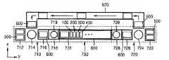
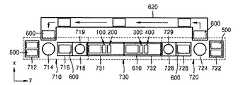
図1は、本発明の一実施形態に関する薄膜蒸着装置を概略的に示すシステム構成図であり、図2は、図1の変形例を示すものである。図3は、静電チャック600の一例を示す概略図である。 FIG. 1 is a system configuration diagram schematically showing a thin film deposition apparatus according to an embodiment of the present invention, and FIG. 2 shows a modification of FIG. FIG. 3 is a schematic diagram illustrating an example of the
図1を参照すれば、本発明の一実施形態による薄膜蒸着装置は、ローディング部710、蒸着部730、アンローディング部720、第1循環部610及び第2循環部620を備える。 Referring to FIG. 1, the thin film deposition apparatus according to an embodiment of the present invention includes a
ローディング部710は、第1ラック712と、導入ロボット714と、導入室716と、第1反転室718と、を備える。 The
第1ラック712には、蒸着が行われる前の基板500が複数積載されており、導入ロボット714は、前記第1ラック712から基板500を捉えて第2循環部620から移送されてきた静電チャック600に基板500を載置した後、基板500が付着された静電チャック600を導入室716に移す。 A plurality of
導入室716に隣接して第1反転室718が備えられ、第1反転室718に位置している第1反転ロボット719が静電チャック600を反転させて、静電チャック600を蒸着部730の第1循環部610に装着する。 A first reversing
静電チャック600は、図3に示したように、セラミックで形成された本体601の内部に電源が印加される電極602が埋め込まれたものであり、この電極602に高電圧が印加されることで本体601の表面に基板500を付着させる。 As shown in FIG. 3, the
図1に示したように、導入ロボット714は、静電チャック600の上面に基板500を載置し、この状態で静電チャック600は導入室716に移送され、第1反転ロボット719が静電チャック600を反転させることで、蒸着部730では基板500が下向きに位置する。 As shown in FIG. 1, the
アンローディング部720の構成は、前述したローディング部710の構成と逆に構成される。すなわち、蒸着部730を経た基板500及び静電チャック600を、第2反転室728で第2反転ロボット729が反転させて搬出室726に移送し、搬出ロボット724が搬出室726から基板500及び静電チャック600を取り出した後、基板500を静電チャック600から分離して第2ラック722に積載する。基板500と分離された静電チャック600は、第2循環部620を通じてローディング部710に回送される。 The configuration of the
しかし、本発明は必ずしもこれらに限定されるものではなく、基板500が静電チャック600に最初に固定される時から、静電チャック600の下面に基板500を固定させてそのまま蒸着部730に移送させてもよい。この場合、例えば、第1反転室718及び第1反転ロボット719と、第2反転室728及び第2反転ロボット729と、は不要になる。 However, the present invention is not necessarily limited to these. From the time when the
蒸着部730は、少なくとも一つの蒸着用チャンバを備える。図1による本発明の望ましい一実施形態によれば、前記蒸着部730は第1チャンバ731を備え、この第1チャンバ731内に複数の薄膜蒸着アセンブリー100、200、300、400が配される。図1に示した本発明の望ましい一実施形態によれば、前記第1チャンバ731内に第1薄膜蒸着アセンブリー100、第2薄膜蒸着アセンブリー200、第3薄膜蒸着アセンブリー300及び第4薄膜蒸着アセンブリー400の4つの薄膜蒸着アセンブリーが設けられているが、その数字は、蒸着物質及び蒸着条件によって可変されうる。前記第1チャンバ731は、蒸着が行われる間、真空に維持される。 The
また、図2による本発明の他の一実施形態によれば、前記蒸着部730は互いに連係された第1チャンバ731及び第2チャンバ732を備え、第1チャンバ731には第1及び第2薄膜蒸着アセンブリー100、200が、第2チャンバ732には第3及び第4薄膜蒸着アセンブリー300、400が配される。この時、チャンバの数が追加されうるということはいうまでもない。 In addition, according to another embodiment of the present invention according to FIG. 2, the
一方、図1による本発明の望ましい一実施形態によれば、前記基板500が固定された静電チャック600は、第1循環部610により少なくとも蒸着部730に、望ましくは、前記ローディング部710、蒸着部730及びアンローディング部720に順次移動し、前記アンローディング部720で基板500と分離された静電チャック600は、第2循環部620により前記ローディング部710に取り戻される。 Meanwhile, according to an exemplary embodiment of the present invention according to FIG. 1, the
前記第1循環部610は、前記蒸着部730を通過する時に前記第1チャンバ731を貫通するように備えられ、前記第2循環部620は、静電チャックが移送されるように備えられる。 The
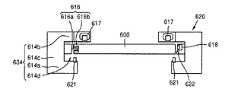
図4は、本発明の望ましい一実施形態による第1循環部610の断面を示したものである。 FIG. 4 is a cross-sectional view of the
第1循環部610は、基板500を固定している静電チャック600を移動させる役割を行う。第1循環部610は、フレーム611、下部プレート613、第1ガイド部614、及びシート支持台615を備える。 The
フレーム611は、第1循環部610の基底部をなし、中空の箱状に形成される。ここで、下部プレート613はフレーム611の下部面を形成し、下部プレート613上には蒸着源10が配される。フレーム611と下部プレート613とは別途の部材に形成されて結合されてもよく、最初から一体型に形成されてもよい。 The
図面には図示されていないが、蒸着源10が配された下部プレート613はカセット形式に形成されて、フレーム611から外部に引出されるように形成されてもよい。従って、蒸着源10の入れ替えが容易になる。 Although not shown in the drawing, the
一方、シート支持台615は、フレーム611の内面から突設され、パターニングスリットシート150を支持する役割を行える。また、シート支持台615は、蒸着源ノズルを通じて排出される蒸着物質が分散されないように、蒸着物質の移動経路をガイドすることもできる。 On the other hand, the
第1ガイド部614はフレーム611上に配され、静電チャック600が一方向に移動するようにガイドする役割を行う。第1ガイド部614は、蒸着部730の第1チャンバ731を貫通して設けられる。 The first guide unit 614 is disposed on the
第1ガイド部614は、静電チャック600の両側を収容して静電チャック600が移動できるようにガイドする。第1ガイド部614は、静電チャック600の下に配される第1収容部614a、静電チャック600の上に配される第2収容部614b、及び第1収容部614aと第2収容部614bとを連結する連結部614cを備える。第1収容部614a、第2収容部614b、及び連結部614cにより収容溝614dが形成される。静電チャック600の一側が収容溝614dに収容され、収容溝614dに沿って静電チャック600が移動する。 The first guide unit 614 accommodates both sides of the
収容溝614d内の連結部614cの一側には静電チャック600の一側に対応するように駆動部616が配され、静電チャック600の他側に対応するように側面磁気浮上軸受618が配される。 A
駆動部616はリニアモータでありうる。リニアモータは、従来の滑り案内システムに比べて摩擦係数が小さくて位置誤差がほとんど発生せず、位置決定精度が非常に高い装置である。リニアモータは、コイル616aとマグネチックレール616bとで形成される。コイル616aは、第1ガイド部614の連結部614cの一側に配され、マグネチックレール616bは、コイル616aに対応して静電チャック600の一側に配される。移動物体である静電チャック600にコイル616aではなくマグネチックレール616bが配されるので、静電チャック600に電源を印加しなくても静電チャック600の駆動が可能である。 The driving
側面磁気浮上軸受618は、静電チャック600の他側に対応するように第1ガイド部614の連結部614c内に配される。側面磁気浮上軸受618は、静電チャック600と第1ガイド部614との間隔を発生させて、静電チャック600が移動する時に第1ガイド部614と接触せずに非接触方式で第1ガイド部614に沿って移動させる役割を行う。 The side magnetic levitation bearing 618 is disposed in the connecting
また、上部磁気浮上軸受617は、静電チャック600の上に位置するように第2収容部614bに配される。上部磁気浮上軸受617は、静電チャック600が第1収容部614a及び第2収容部614bに接触せずにこれらと一定の間隔を維持しながら第1ガイド部614に沿って移動させる役割を行う。図面には図示されていないが、磁気浮上軸受は、静電チャック600の下部に対応するように第1収容部614aに配されてもよい。 The upper magnetic levitation bearing 617 is disposed in the
第1ガイド部614はギャップセンサー621をさらに備える。ギャップセンサー621は、静電チャック600と第1ガイド部614との間隔を測定できる。図4を参照すれば、ギャップセンサー621は、静電チャック600の下部に対応するように第1収容部614aに配される。第1収容部614aに配されたギャップセンサー621は、第1収容部614aと静電チャック600との間隔を測定できる。また、側面磁気浮上軸受618にもギャップセンサー622が配される。側面磁気浮上軸受618に配されたギャップセンサー622は、静電チャック600の側面と側面磁気浮上軸受618との間隔を測定できる。本発明はこれらに限定されるものではなく、ギャップセンサー622は連結部614cに配されうる。 The first guide unit 614 further includes a
ギャップセンサー621、622により測定された値によって磁気浮上軸受617、618の磁気力が変更されて、静電チャック600と第1ガイド部614との間隔がリアルタイムで調節される。磁気浮上軸受617、618とギャップセンサー621、622とを用いるフィードバック制御により静電チャック600の精密移動が可能である。 The magnetic force of the
図5は、本発明の一実施形態による第2循環部620の断面を示すものである。 FIG. 5 illustrates a cross section of the
第2循環部620は、基板500が分離された静電チャック600を移動させる第2ガイド部634を備える。 The
第2ガイド部634は、第1収容部614a、第2収容部614b及び連結部614cを備える。第1収容部614a、第2収容部614b及び連結部614cにより形成された収容溝614dに静電チャック600が収容され、静電チャック600は収容溝614dに沿って移動する。 The second guide part 634 includes a first
静電チャック600の一側に対応するように、連結部614cに駆動部616が配される。駆動部616は、第2ガイド部634に沿って静電チャック600を移動させる駆動力を発生させる。駆動部616はリニアモータであり、連結部614cに配されるコイル616aと、前記コイル616aに対応するように静電チャック600の一側に配されるマグネチックレール616bとを備える。 A driving
側面磁気浮上軸受618は、静電チャック600の他側に対応するように第2ガイド部634の連結部614c内に配される。上部磁気浮上軸受617は、静電チャック600の上に位置するように第2収容部614bに配される。磁気浮上軸受617、618は、静電チャック600と第2ガイド部634との間隔を発生させて静電チャック600が移動する時、第2ガイド部634と接触せずに非接触方式で第2ガイド部634に沿って移動させる役割を行う。 The side magnetic levitation bearing 618 is disposed in the connecting
第2循環部620は、静電チャック600と第2ガイド部634との間隔を測定するために、ギャップセンサー621、622をさらに備える。ギャップセンサー621は、静電チャック600の下部に対応するように第1収容部614aに配され、静電チャック600の側部に対応するように側面磁気浮上軸受618上に配される。 The
次いで、本発明の一実施形態による有機層蒸着装置の有機層蒸着アセンブリー100を説明する。図6は、図1の有機層蒸着装置の有機層蒸着アセンブリーを概略的に示す斜視図であり、図7は、図6の有機層蒸着アセンブリーの概略的な側断面図であり、図8は、図6の有機層蒸着アセンブリーの概略的な平断面図である。 Next, the organic
図6ないし図8を参照すれば、本発明の一実施形態に関する有機層蒸着アセンブリー100は、蒸着源110、蒸着源ノズル部120、遮断板アセンブリー130及びパターニングスリットシート150を備える。 6 to 8, the organic
ここで、図6ないし図8には、説明の便宜のためにチャンバを示していないが、図6ないし図8のあらゆる構成は、適当な真空度が維持されるチャンバ内に配されることが望ましい。これは、蒸着物質の直進性を確保するためである。 Here, the chamber is not shown in FIGS. 6 to 8 for convenience of explanation, but any configuration of FIGS. 6 to 8 may be arranged in a chamber in which an appropriate degree of vacuum is maintained. desirable. This is to ensure straightness of the vapor deposition material.
かかるチャンバ内には、被蒸着体である基板500が静電チャック(図1の600参照)により移送される。前記基板500は平板表示装置用基板になりうるが、複数の平板表示装置を形成できるマザーガラスなどの大面積基板が適用される。 In the chamber, a
ここで、本発明の一実施形態では、基板500が有機層蒸着アセンブリー100に対して相対的に移動するが、望ましくは、有機層蒸着アセンブリー100に対して基板500を矢印A方向に移動させることができる。 Here, in one embodiment of the present invention, the
詳細には、既存のFMM蒸着方法では、マスクのサイズが基板サイズと同一か、またはそれより大きくなければならなかった。従って、基板サイズが増大するほどマスクも大型化せねばならないが、かかる大型のマスクの製作が容易でなく、マスクを引っ張って精密なパターンに位置合わせすることも容易でないという問題点があった。 Specifically, in existing FMM deposition methods, the mask size had to be the same as or larger than the substrate size. Therefore, the mask must be enlarged as the substrate size increases, but there is a problem that it is not easy to manufacture such a large mask and it is not easy to pull the mask and align it with a precise pattern.
これらの問題点を解決するために、本発明の一実施形態に関する有機層蒸着アセンブリー100は、有機層蒸着アセンブリー100と基板500とが互いに相対的に移動しつつ蒸着が行われることを一特徴とする。言い換えれば、有機層蒸着アセンブリー100と対向して配された基板500がY軸方向に沿って移動しつつ連続的に蒸着を行う。すなわち、基板500が図6の矢印A方向に移動しつつスキャニング方式で蒸着が行われる。ここで、図面には、基板500がチャンバ(図1の731参照)内でY軸方向に移動しつつ蒸着が行われると図示されているが、本発明の思想はこれに制限されず、基板500は固定されており、有機層蒸着アセンブリー100自体がY軸方向に移動しつつ蒸着を行うこともできるといえる。 In order to solve these problems, an organic
従って、本発明の有機層蒸着アセンブリー100では、従来のFMMに比べて非常に小さくパターニングスリットシート150を作ることができる。すなわち、本発明の有機層蒸着アセンブリー100の場合、基板500がY軸方向に沿って移動しつつ連続的に、すなわち、スキャニング方式で蒸着を行うため、パターニングスリットシート150のX軸方向への幅と、基板500のX軸方向への幅のみ実質的に同一に形成されれば、パターニングスリットシート150のY軸方向の長さは、基板500の長さより非常に小さく形成されてもよい。もちろん、パターニングスリットシート150のX軸方向への幅が基板500のX軸方向への幅より小さく形成されても、基板500と有機層蒸着アセンブリー100との相対的移動によるスキャニング方式により、十分に基板500全体に対して蒸着を行えるようになる。 Therefore, in the organic
このように、従来のFMMに比べて非常に小さくパターニングスリットシート150を作ることができるため、本発明のパターニングスリットシート150はその製造が容易である。すなわち、パターニングスリットシート150のエッチング作業や、その後の精密引っ張り及び溶接作業、移動及び洗浄作業などのあらゆる工程で、小さなサイズのパターニングスリットシート150がFMM蒸着方法に比べて有利である。また、これはディスプレイ装置が大型化するほどさらに有利になる。 Thus, since the
このように、有機層蒸着アセンブリー100と基板500とが互いに相対的に移動しつつ蒸着が行われるためには、有機層蒸着アセンブリー100と基板500とが一定間隔だけ離隔することが望ましい。これについては後述する。 As described above, in order to perform deposition while the organic
一方、チャンバ内で前記基板500と対向する側には、蒸着物質115が収納及び加熱される蒸着源110が配される。 Meanwhile, a
前記蒸着源110は、その内部に蒸着物質115が満たされる坩堝112と、この坩堝112を取り囲む冷却ブロック111が備えられる。冷却ブロック111は、坩堝112からの熱が外部、すなわち、チャンバ内部に発散されることを最大限抑制するためのものであり、この冷却ブロック111には、坩堝112を加熱させるヒータ(図示せず)が備えられている。 The
蒸着源110の一側、さらに詳細には、蒸着源110から基板500に向かう側には蒸着源ノズル部120が配される。そして、蒸着源ノズル部120には、X軸方向に沿って複数の蒸着源ノズル121が形成される。ここで、前記複数の蒸着源ノズル121は等間隔で形成される。蒸着源110内で気化した蒸着物質115は、これらの蒸着源ノズル部120の蒸着源ノズル121を通過して、被蒸着体である基板500側に向かう。 The vapor deposition
蒸着源ノズル部120の一側には遮断板アセンブリー130が備えられる。前記遮断板アセンブリー130は、複数の遮断板131と、遮断板131の外側に備えられる遮断板フレーム132とを備える。前記複数の遮断板131は、X軸方向に沿って互いに平行に配される。ここで、前記複数の遮断板131は等間隔で形成される。また、それぞれの遮断板131は、図面によれば、YZ平面に沿って延びており、望ましくは、長方形に形成される。このように配された複数の遮断板131は、蒸着源ノズル部120とパターニングスリットシート150との間の空間を複数の蒸着空間Sに区切る。すなわち、本発明の一実施形態に関する有機層蒸着アセンブリー100は前記遮断板131によって、図8に示したように、蒸着物質が噴射されるそれぞれの蒸着源ノズル121別に蒸着空間Sが分離される。 A
ここで、それぞれの遮断板131は互いに隣接している蒸着源ノズル121の間に配される。これは、言い換えれば、互いに隣接している遮断板131の間に一つの蒸着源ノズル121が配されることである。望ましくは、蒸着源ノズル121は、互いに隣接している遮断板131間の中央に位置できる。しかし、本発明は必ずしもこれに限定されず、互いに隣接している遮断板131の間に複数の蒸着源ノズル121を配置してもよい。ただし、この場合にも、複数の蒸着源ノズル121を、互いに隣接している遮断板131の間の中央に位置させることが望ましい。 Here, each shielding
このように、遮断板131が蒸着源ノズル部120とパターニングスリットシート150との間の空間を複数の蒸着空間Sに区切ることで、一つの蒸着源ノズル121から排出される蒸着物質は他の蒸着源ノズル121から排出された蒸着物質と混合されず、パターニングスリット151を通過して基板500に蒸着される。すなわち、前記遮断板131は、各蒸着源ノズル121を通じて排出される蒸着物質が分散されずにY軸方向に直進するように蒸着物質の移動経路をガイドする役割を行う。 As described above, the
このように、遮断板131を備えて蒸着物質の直進性を確保することで、基板に形成される陰影(shadow)の大きさを大きく縮めることができ、従って、有機層蒸着アセンブリー100と基板500とを一定間隔だけ離隔させることができる。これについては、後述する。 As described above, by providing the
一方、蒸着源110と基板500との間にはパターニングスリットシート150及びフレーム155がさらに備えられる。前記フレーム155は窓枠状に形成され、その内側にパターニングスリットシート150が結合される。そして、パターニングスリットシート150には、X軸方向に沿って複数のパターニングスリット151が形成される。各パターニングスリット151はY軸方向に沿って延びている。蒸着源110内で気化して蒸着源ノズル121を通過した蒸着物質115は、パターニングスリット151を通過して被蒸着体である基板500側に向かう。 Meanwhile, a
前記パターニングスリットシート150は金属薄板で形成され、引っ張られた状態でフレーム155に固定される。前記パターニングスリット151はストライプタイプであって、パターニングスリットシート150にエッチングにより形成される。ここで、前記パターニングスリット151の数は、基板500に形成される蒸着パターンの数に対応させることが望ましい。 The
一方、前述した遮断板アセンブリー130とパターニングスリットシート150とは、互いに一定間隔だけ離隔して形成され、遮断板アセンブリー130とパターニングスリットシート150とは、別途の連結部材135によって互いに連結される。 Meanwhile, the blocking
前述したように、本発明の一実施形態に関する有機層蒸着アセンブリー100は、基板500に対して相対的に移動しつつ蒸着を行い、このように有機層蒸着アセンブリー100が基板500に対して相対的に移動するために、パターニングスリットシート150は基板500から一定間隔だけ離隔して形成される。そして、パターニングスリットシート150と基板500とを離隔させる場合に発生する陰影問題を解決するために、蒸着源ノズル部120とパターニングスリットシート150との間に遮断板131を備えて蒸着物質の直進性を確保することで、基板に形成される陰影の大きさを大きく縮める。 As described above, the organic
従来のFMM蒸着方法では、基板に陰影を発生させないために、基板にマスクを密着させて蒸着工程を進めた。しかし、このように基板にマスクを密着させる場合、基板とマスクとの接触により基板に既に形成されていたパターンにスクラッチなどの不良問題が発生するという問題点があった。また、マスクを基板に対して移動させられないため、マスクが基板と同じ大きさに形成されねばならない。従って、ディスプレイ装置の大型化につれてマスクの大きさも大きくならねばならないが、かような大型マスクの形成が容易ではないという問題点があった。 In the conventional FMM vapor deposition method, in order not to generate a shadow on the substrate, the vapor deposition process was performed with the mask adhered to the substrate. However, when the mask is brought into close contact with the substrate in this way, there is a problem that a defect such as a scratch occurs in the pattern already formed on the substrate due to the contact between the substrate and the mask. In addition, since the mask cannot be moved with respect to the substrate, the mask must be formed in the same size as the substrate. Therefore, although the size of the mask has to be increased as the display device becomes larger, there is a problem that it is not easy to form such a large mask.
これらの問題点を解決するために、本発明の一実施形態に関する有機層蒸着アセンブリー100では、パターニングスリットシート150が被蒸着体である基板500と所定間隔をおいて離隔して配されるようにする。これは、遮断板131を備えて、基板500に生成される陰影が小さくなることで実現可能になる。 In order to solve these problems, in the organic
このような有機層蒸着装置を用いて有機発光ディスプレイ装置の有機層などの薄膜を形成できるが、これについては図12で詳細に説明する。 A thin film such as an organic layer of an organic light emitting display device can be formed using such an organic layer deposition apparatus, which will be described in detail with reference to FIG.
図9は、本発明の他の一実施形態に関する有機層蒸着アセンブリーを概略的に示す斜視図である。 FIG. 9 is a perspective view schematically illustrating an organic layer deposition assembly according to another embodiment of the present invention.
図9に示した実施形態に関する有機層蒸着アセンブリー800は、蒸着源810、蒸着源ノズル部820、第1遮断板アセンブリー830、第2遮断板アセンブリー840及びパターニングスリットシート850を備える。ここで、蒸着源810、第1遮断板アセンブリー830及びパターニングスリットシート850の詳細な構成は、前述した図6による実施形態と同一であるので詳細な説明を省略する。本実施形態では、第1遮断板アセンブリー830の一側に第2遮断板アセンブリー840が備えられるという点で、前述した実施形態と区別される。 The organic
詳細には、前記第2遮断板アセンブリー840は、複数の第2遮断板841と、第2遮断板841の外側に備えられる第2遮断板フレーム842とを備える。前記複数の第2遮断板841は、X軸方向に沿って互いに平行に備えられる。そして、前記複数の第2遮断板841は等間隔で形成される。また、それぞれの第2遮断板841は、図面からみればYZ平面と平行に、言い換えれば、X軸方向に垂直になるように形成される。 In detail, the second shield plate assembly 840 includes a plurality of second shield plates 841 and a second shield plate frame 842 provided outside the second shield plate 841. The plurality of second blocking plates 841 are provided in parallel to each other along the X-axis direction. The plurality of second blocking plates 841 are formed at equal intervals. Each of the second blocking plates 841 is formed to be parallel to the YZ plane when viewed from the drawing, in other words, to be perpendicular to the X-axis direction.
このように配された複数の第1遮断板831及び第2遮断板841は、蒸着源ノズル部820とパターニングスリットシート850との間の空間を区切る役割を行う。すなわち、前記第1遮断板831及び第2遮断板841によって、蒸着物質が噴射されるそれぞれの蒸着源ノズル821別に蒸着空間が分離されることを一特徴とする。 The plurality of
ここで、それぞれの第2遮断板841は、それぞれの第1遮断板831と一対一対応して配される。言い換えれば、それぞれの第2遮断板841は、それぞれの第1遮断板831と整列されて互いに平行に配される。すなわち、互いに対応する第1遮断板831と第2遮断板841とは互いに同じ平面上に位置する。図面には、第1遮断板831の厚さと第2遮断板841のX軸方向の幅とが同一であると図示されているが、本発明の思想はこれに制限されるものではない。すなわち、パターニングスリット851との精密な位置決定が求められる第2遮断板841は相対的に薄く形成される一方、精密な位置決定が求められていない第1遮断板831は相対的に厚く形成されて、その製造を容易にすることもできるといえる。 Here, the respective second blocking plates 841 are arranged in one-to-one correspondence with the respective
図10は、本発明のさらに他の一実施形態による有機層蒸着アセンブリーを概略的に示す斜視図である。 FIG. 10 is a perspective view schematically illustrating an organic layer deposition assembly according to another embodiment of the present invention.
図10を参照すれば、本発明のさらに他の一実施形態による有機層蒸着アセンブリー900は、蒸着源910、蒸着源ノズル部920及びパターニングスリットシート950を備える。 Referring to FIG. 10, an organic
ここで、蒸着源910は、その内部に蒸着物質915が満たされる坩堝911と、坩堝911を加熱させて坩堝911の内部に満たされた蒸着物質915を蒸着源ノズル部920側に蒸発させるためのヒータ912と、を備える。一方、蒸着源910の一側には蒸着源ノズル部920が配され、蒸着源ノズル部920には、Y軸方向に沿って複数の蒸着源ノズル921が形成される。一方、蒸着源910と基板500との間には、パターニングスリットシート950及びフレーム955がさらに備えられ、パターニングスリットシート950には、X軸方向に沿って複数のパターニングスリット951が形成される。そして、蒸着源910及び蒸着源ノズル部920とパターニングスリットシート950とは、連結部材935によって結合される。 Here, the
本実施形態は、前述した実施形態に比べて蒸着源ノズル部920に備えられた複数の蒸着源ノズル921の配置が異なるため、これについて詳細に説明する。 In the present embodiment, since the arrangement of the plurality of vapor
蒸着源910の一側、詳細には、蒸着源910から基板500に向かう側には蒸着源ノズル部920が配される。そして、蒸着源ノズル部920には、Y軸方向、すなわち、基板500のスキャン方向に沿って複数の蒸着源ノズル921が形成される。ここで、前記複数の蒸着源ノズル921は等間隔で形成される。蒸着源910内で気化した蒸着物質915は、これらの蒸着源ノズル部920を通過して被蒸着体である基板500側に向かう。このように、蒸着源ノズル部920上にY軸方向、すなわち、基板500のスキャン方向に沿って複数の蒸着源ノズル921が形成する場合、パターニングスリットシート950のそれぞれのパターニングスリット951を通過する蒸着物質により形成されるパターンの大きさは、蒸着源ノズル921一つの大きさのみにより影響されるので(すなわち、X軸方向には蒸着源ノズル921が一つだけ存在することになるので)、陰影が発生しなくなる。また、複数の蒸着源ノズル921がスキャン方向に存在するので、個別の蒸着源ノズルの間にフラックス(flux)差が発生しても、その差が相殺されて蒸着均一度が一定に維持される効果を得る。 A vapor deposition
図11は、本発明のさらに他の一実施形態による有機層蒸着アセンブリーを示す図面である。図面を参照すれば、本発明のさらに他の一実施形態による有機層蒸着アセンブリーは、蒸着源910、蒸着源ノズル部920及びパターニングスリットシート950を備える。 FIG. 11 is a view illustrating an organic layer deposition assembly according to another embodiment of the present invention. Referring to the drawings, an organic layer deposition assembly according to another embodiment of the present invention includes a
本実施形態では、蒸着源ノズル部920に形成された複数の蒸着源ノズル921が所定角度だけチルトされて配されるという点で、前述した実施形態と区別される。詳細には、蒸着源ノズル921は2列の蒸着源ノズル921a、921bで形成され、前記2列の蒸着源ノズル921a、921bは互いに交互に配される。この時、蒸着源ノズル921a、921bは、XZ平面上で所定角度だけ傾いて形成される。 The present embodiment is distinguished from the above-described embodiments in that a plurality of vapor
すなわち、本実施形態では、蒸着源ノズル921a、921bが所定角度だけ傾いて配される。ここで、第1列の蒸着源ノズル921aは、第2列の蒸着源ノズル921bに向かうようにチルトされ、第2列の蒸着源ノズル921bは、第1列の蒸着源ノズル921aに向かうようにチルトされる。言い換えれば、左側列に配された蒸着源ノズル921aは、パターニングスリットシート950の右側端部に向かうように配され、右側列に配された蒸着源ノズル921bは、パターニングスリットシート950の左側端部に向かうように配される。 That is, in this embodiment, the vapor
このような構成によって、基板の中央と端部とにおける成膜厚さの差が低減して全体的な蒸着物質の厚さが均一になるように蒸着量を制御でき、さらには材料利用効率が向上する効果を得る。 With such a configuration, the deposition amount can be controlled so that the difference in film thickness between the center and the edge of the substrate is reduced, and the thickness of the entire deposition material is uniform, and the material utilization efficiency is further improved. Get an improved effect.
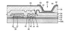
図12は、本発明の有機層蒸着装置を用いて製造されたアクティブマトリックス型有機発光ディスプレイ装置の断面を示すものである。 FIG. 12 shows a cross section of an active matrix organic light emitting display device manufactured using the organic layer deposition apparatus of the present invention.
図12を参照すれば、前記アクティブマトリックス型の有機発光ディスプレイ装置は基板500上に形成される。前記基板500は、透明な素材、例えば、ガラス材、プラスチック材、または金属材で形成される。前記基板500上には、全体的にバッファ層などの絶縁膜31が形成されている。 Referring to FIG. 12, the active matrix organic light emitting display device is formed on a
前記絶縁膜31上には、図12に示したようなTFT40と、キャパシタ50と、有機発光素子60とが形成される。 A
前記絶縁膜31の上面には、所定パターンに配列された半導体活性層41が形成されている。前記半導体活性層41は、ゲート絶縁膜32によって埋め込まれている。前記活性層41は、p型またはn型の半導体からなる。 A semiconductor
前記ゲート絶縁膜32の上面には、前記活性層41と対応する位置にTFT40のゲート電極42が形成される。そして、前記ゲート電極42を覆うように層間絶縁膜33が形成される。前記層間絶縁膜33が形成された後には、ドライエッチングなどのエッチング工程によって前記ゲート絶縁膜32と層間絶縁膜33とをエッチングしてコンタクトホールを形成させて、前記活性層41の一部を露出させる。 A
次いで、前記層間絶縁膜33上にソース/ドレイン電極43が形成されるが、コンタクトホールを通じて露出された活性層41に接触するように形成される。前記ソース/ドレイン電極43を覆うように保護膜34が形成され、エッチング工程を通じて前記ドレイン電極43の一部を露出させる。前記保護膜34上には、保護膜34の平坦化のために別途の絶縁膜をさらに形成してもよい。 Next, a source /
一方、前記有機発光素子60は、電流の印加によって赤色、緑色、青色の光を発光して所定の画像情報を表示するためのものであり、前記保護膜34上に第1電極61を形成する。前記第1電極61は、TFT40のドレイン電極43と電気的に連結される。 On the other hand, the organic
次いで、前記第1電極61を覆うように画素定義膜35が形成される。この画素定義膜35に所定の開口を形成した後、この開口に限定された領域内に発光層を含む有機層63を形成する。そして、有機層63上には第2電極62を形成する。 Next, a
前記画素定義膜35は各画素を区切るものであり、有機物で形成されて、第1電極61が形成されている基板の表面、特に、保護膜34の表面を平坦化する。 The
前記第1電極61と第2電極62とは互いに絶縁されており、発光層を含む有機層63に相異なる極性の電圧を加えて発光が行われるようにする。 The
前記発光層を含む有機層63には、低分子または高分子有機物が使われるが、低分子有機物を使用する場合にホール注入層(HIL:Hole Injection Layer)、ホール輸送層(HTL:Hole Transport Layer)、発光層(EML:Emission Layer)、電子輸送層(ETL:Electron Transport Layer)、電子注入層(EIL:Electron Injection Layer)などが単一あるいは複合の構造で積層されて形成され、使用可能な有機材料も銅フタロシアニン(CuPc)、N,N−ジ(ナフタレン−1−イル)−N,N’−ジフェニル−ベンジジン(NPB)、トリス−8−ヒドロキシキノリンアルミニウム(Alq3)などをはじめとして多様に適用できる。 For the
これらの有機発光膜を形成した後には、第2電極62も同じ蒸着工程で形成できる。 After these organic light emitting films are formed, the
一方、前記第1電極61はアノード電極の機能を行い、前記第2電極62はカソード電極の機能を行うが、もちろん、これら第1電極61と第2電極62との極性は逆になってもよい。そして、第1電極61は、各画素の領域に対応するようにパターニングされ、第2電極62は、あらゆる画素を覆うように形成される。 Meanwhile, the
前記第1電極61は、透明電極または反射型電極として備えられるが、透明電極として使われる時には、ITO、IZO、ZnO、またはIn2O3からなり、反射型電極として使われる時には、Ag、Mg、Al、Pt、Pd、Au、Ni、Nd、Ir、Cr、及びこれらの化合物で反射層を形成した後、その上にITO、IZO、ZnO、またはIn2O3で透明電極層を形成できる。これらの第1電極61は、スパッタリング方法などにより成膜された後、フォトリソグラフィ法などによりパターニングされる。The
一方、前記第2電極62も、透明電極または反射型電極として備えられるが、透明電極として使われる時には、この第2電極62がカソード電極として使われるので、仕事関数の小さな金属、すなわち、Li、Ca、LiF/Ca、LiF/Al、Al、Ag、Mg、及びこれらの化合物が発光層を含む有機層63の方向に向かうように蒸着した後、その上にITO、IZO、ZnO、またはIn2O3などで補助電極層やバス電極ラインを形成できる。そして、反射型電極として使われる時には、前記のLi、Ca、LiF/Ca、LiF/Al、Al、Ag、Mg、及びこれらの化合物を全面蒸着して形成する。この時、蒸着は、前述した発光層を含む有機層63の場合と同じ方法で行える。On the other hand, the
一方、前記第2電極62上には保護層64がさらに形成される。保護層64は第2電極62の上部に形成されて、画素領域以外の領域の有機層63を除去する過程でマスクの役割を行うと同時に第2電極62を保護する役割を行う。 Meanwhile, a
本発明はこれ以外にも、有機TFTの有機膜または無機膜などの蒸着にも使用でき、その他の多様な素材の成膜工程に適用できる。 In addition to this, the present invention can be used for vapor deposition of an organic film or an inorganic film of an organic TFT, and can be applied to a film forming process of various other materials.
本明細書では本発明を限定された実施形態を中心として説明したが、本発明の範囲内で多様な実施形態が可能である。また説明されていないが、均等な手段もまた本発明にそのまま結合されるといえる。従って、本発明の真の保護範囲は特許請求の範囲によって定められねばならない。 Although the present invention has been described herein with a focus on limited embodiments, various embodiments are possible within the scope of the invention. Although not described, it can be said that equivalent means are also directly coupled to the present invention. Therefore, the true protection scope of the present invention must be determined by the claims.
本発明は、有機層蒸着装置及びこれを用いる有機発光表示装置関連の技術分野に好適に用いられる。 INDUSTRIAL APPLICABILITY The present invention is suitably used in the technical field related to an organic layer deposition apparatus and an organic light emitting display using the same.
100 有機層蒸着アセンブリー
110 蒸着源
120 蒸着源ノズル部
150 パターニングスリットシート
500 基板
600 静電チャック
61 第1電極
62 第2電極
63 有機層
64 保護層DESCRIPTION OF
Claims (19)
Translated fromJapanese真空に維持されるチャンバ及び前記チャンバの内部に配されて前記静電チャックに固定された前記基板に薄膜を蒸着する薄膜蒸着アセンブリーを備える蒸着部と、
前記基板が固定された前記静電チャックを前記蒸着部内に移動させる第1循環部と、を備え、
前記第1循環部が、前記蒸着部を通過する時に前記チャンバ内部に貫通し、
前記第1循環部が、前記静電チャックが一方向に移動可能に前記静電チャックの端部を収容する収容部を備えるガイド部を備え、
前記収容部が、前記静電チャックの下に配される第1収容部と、前記静電チャックの上に配される第2収容部と、前記第1収容部と前記第2収容部とを連結する連結部を備えることを特徴とする、有機層蒸着装置。An electrostatic chuck for fixing the substrate for vapor deposition;
A deposition unit comprising a chamber maintained in a vacuum and a thin film deposition assembly disposed in the chamber and depositing a thin film on the substrate fixed to the electrostatic chuck;
A first circulation unit that moves the electrostatic chuck to which the substrate is fixed into the vapor deposition unit,
The first circulation part penetrates into the chamber when passing through the vapor deposition part,
The first circulation unit includesa guide unit including a storage unit that storesan end of the electrostatic chuck so that the electrostatic chuck can move in one direction.
The housing portion includes a first housing portion disposed below the electrostatic chuck, a second housing portion disposed on the electrostatic chuck, the first housing portion, and the second housing portion. An organic layer deposition apparatus comprisinga connecting portion for connecting .
前記静電チャックから蒸着の完了した前記基板を分離させるアンローディング部と、をさらに備える、請求項1に記載の有機層蒸着装置。A loading unit for fixing the substrate to the electrostatic chuck;
The organic layer deposition apparatus according to claim 1, further comprising: an unloading unit that separates the substrate on which deposition has been completed from the electrostatic chuck.
前記静電チャックを移動させられるように駆動力を発生させる駆動部と、
前記静電チャックが前記収容部と非接触で移動できるように、前記収容部で浮上させる磁気浮上軸受と、を備えることを特徴とする、請求項1に記載の有機層蒸着装置。The guide portion is
A driving unit that generates a driving force to move the electrostatic chuck;
The organic layer deposition apparatus according to claim 1, further comprising: a magnetic levitation bearing that floats on the housing portion so that the electrostatic chuck can move without contact with the housing portion.
蒸着物質を放射する蒸着源と、
前記蒸着源の一側に配され、第1方向に沿って複数の蒸着源ノズルが形成される蒸着源ノズル部と、
前記蒸着源ノズル部と対向して配され、前記第1方向に対して垂直の第2方向に沿って複数のパターニングスリットが形成されるパターニングスリットシートと、を備え、
前記基板が、前記有機層蒸着アセンブリーと所定距離だけ離隔して配置されて、前記有機層蒸着アセンブリーに対して相対的に移動可能に配置されることを特徴とする、請求項1に記載の有機層蒸着装置。The thin film deposition assembly comprises:
A deposition source that radiates the deposition material;
A vapor deposition source nozzle part disposed on one side of the vapor deposition source, wherein a plurality of vapor deposition source nozzles are formed along a first direction;
A patterning slit sheet that is arranged opposite to the vapor deposition source nozzle part and has a plurality of patterning slits formed along a second direction perpendicular to the first direction,
The organic material according to claim 1, wherein the substrate is disposed at a predetermined distance from the organic layer deposition assembly and is movable relative to the organic layer deposition assembly. Layer deposition equipment.
前記基板が固定された前記静電チャックを、チャンバを貫通して設けられた第1循環部を用いて真空に維持される前記チャンバ内に移送する段階と、
前記チャンバ内に配された薄膜蒸着アセンブリーを用い、前記基板と前記薄膜蒸着アセンブリーとの相対的な移動により前記基板に有機膜を蒸着する段階と、を備え、
前記静電チャックが、前記第1循環部と非接触方式で前記チャンバ内を移送され、
前記第1循環部が、前記静電チャックが一方向に移動可能に前記静電チャックの端部を収容する収容部を備えるガイド部を備え、
前記収容部が、前記静電チャックの下に配される第1収容部と、前記静電チャックの上に配される第2収容部と、前記第1収容部と前記第2収容部とを連結する連結部を備えることを特徴とする、有機発光表示装置の製造方法。Fixing the substrate with an electrostatic chuck; and
Transferring the electrostatic chuck to which the substrate is fixed into the chamber maintained in a vacuum using a first circulation unit provided through the chamber; and
Using a thin film deposition assembly disposed in the chamber, and depositing an organic film on the substrate by relative movement of the substrate and the thin film deposition assembly.
The electrostatic chuck is transferred in the chamber in a non-contact manner with the first circulation unit,
The first circulation unit includes a guide unit including a storage unit that stores an end of the electrostatic chuck so that the electrostatic chuck can move in one direction.
The housing portion includes a first housing portion disposed below the electrostatic chuck, a second housing portion disposed on the electrostatic chuck, the first housing portion, and the second housing portion. A method for manufacturing an organic light emitting display device, comprisinga connecting portion to beconnected .
前記第1循環部を用いて、蒸着の完了した前記基板を前記チャンバから取り出す段階と、
前記静電チャックから蒸着の完了した前記基板を分離させる段階と、
前記基板と分離された前記静電チャックを、前記チャンバの外部に設けられた第2循環部を用いて前記基板を静電チャックに固定させる段階に取り戻す段階と、をさらに含むことを特徴とする、請求項14に記載の有機発光表示装置の製造方法。After the organic film deposition step,
Using the first circulation unit to take out the substrate after vapor deposition from the chamber;
Separating the deposited substrate from the electrostatic chuck;
The method further comprises the step of returning the electrostatic chuck separated from the substrate to a step of fixing the substrate to the electrostatic chuck using a second circulation unit provided outside the chamber. The method of manufacturing an organic light emitting display device according to claim 14.
蒸着物質を放射する蒸着源と、
前記蒸着源の一側に配され、第1方向に沿って複数の蒸着源ノズルが形成される蒸着源ノズル部と、
前記蒸着源ノズル部と対向して配され、前記第1方向に対して垂直の第2方向に沿って複数のパターニングスリットが形成されるパターニングスリットシートと、を備え、
前記基板が、前記有機層蒸着アセンブリーと所定距離だけ離隔して配置されて、前記有機層蒸着アセンブリーに対して相対的に移動可能に配置されることを特徴とする、請求項14に記載の有機発光表示装置の製造方法。The thin film deposition assembly comprises:
A deposition source that radiates the deposition material;
A vapor deposition source nozzle part disposed on one side of the vapor deposition source, wherein a plurality of vapor deposition source nozzles are formed along a first direction;
A patterning slit sheet that is arranged opposite to the vapor deposition source nozzle part and has a plurality of patterning slits formed along a second direction perpendicular to the first direction,
The organic substrate according to claim 14, wherein the substrate is disposed at a predetermined distance from the organic layer deposition assembly and is movable relative to the organic layer deposition assembly. Manufacturing method of light emitting display device.
Applications Claiming Priority (2)
| Application Number | Priority Date | Filing Date | Title |
|---|---|---|---|
| KR10-2011-0066124 | 2011-07-04 | ||
| KR1020110066124AKR20130004830A (en) | 2011-07-04 | 2011-07-04 | Apparatus for thin layer deposition and method for manufacturing of organic light emitting display apparatus using the same |
Publications (3)
| Publication Number | Publication Date |
|---|---|
| JP2013016491A JP2013016491A (en) | 2013-01-24 |
| JP2013016491A5 JP2013016491A5 (en) | 2015-07-23 |
| JP6037546B2true JP6037546B2 (en) | 2016-12-07 |
Family
ID=46548208
Family Applications (1)
| Application Number | Title | Priority Date | Filing Date |
|---|---|---|---|
| JP2012149279AActiveJP6037546B2 (en) | 2011-07-04 | 2012-07-03 | ORGANIC LAYER DEPOSITION DEVICE AND METHOD FOR MANUFACTURING ORGANIC LIGHT EMITTING DISPLAY |
Country Status (6)
| Country | Link |
|---|---|
| US (2) | US9512515B2 (en) |
| EP (1) | EP2543749B1 (en) |
| JP (1) | JP6037546B2 (en) |
| KR (1) | KR20130004830A (en) |
| CN (2) | CN102867924B (en) |
| TW (1) | TWI570978B (en) |
Families Citing this family (54)
| Publication number | Priority date | Publication date | Assignee | Title |
|---|---|---|---|---|
| JP5677785B2 (en) | 2009-08-27 | 2015-02-25 | 三星ディスプレイ株式會社Samsung Display Co.,Ltd. | Thin film deposition apparatus and organic light emitting display device manufacturing method using the same |
| KR101202348B1 (en) | 2010-04-06 | 2012-11-16 | 삼성디스플레이 주식회사 | Apparatus for thin layer deposition and method for manufacturing of organic light emitting display apparatus using the same |
| JP5562189B2 (en)* | 2010-09-22 | 2014-07-30 | 東京エレクトロン株式会社 | Substrate processing equipment |
| JP2014515789A (en)* | 2011-04-20 | 2014-07-03 | コーニンクレッカ フィリップス エヌ ヴェ | Measuring apparatus and method for vapor deposition applications |
| KR20130004830A (en)* | 2011-07-04 | 2013-01-14 | 삼성디스플레이 주식회사 | Apparatus for thin layer deposition and method for manufacturing of organic light emitting display apparatus using the same |
| KR102013318B1 (en)* | 2012-09-20 | 2019-08-23 | 삼성디스플레이 주식회사 | Apparatus for thin layer deposition, method for manufacturing of organic light emitting display apparatus using the same, and organic light emitting display apparatus |
| KR101971199B1 (en) | 2012-09-21 | 2019-08-14 | 삼성디스플레이 주식회사 | Apparatus for organic layer deposition, organic light emitting display apparatus and method for manufacturing the same |
| KR20140050994A (en)* | 2012-10-22 | 2014-04-30 | 삼성디스플레이 주식회사 | Organic light emitting display apparatus and method for manufacturing the same |
| KR102075525B1 (en)* | 2013-03-20 | 2020-02-11 | 삼성디스플레이 주식회사 | Deposition apparatus for organic layer, method for manufacturing organic light emitting display apparatus using the same, and organic light emitting display apparatus manufactured by the method |
| KR20140118551A (en)* | 2013-03-29 | 2014-10-08 | 삼성디스플레이 주식회사 | Deposition apparatus, method for manufacturing organic light emitting display apparatus and organic light emitting display apparatus |
| KR102081284B1 (en) | 2013-04-18 | 2020-02-26 | 삼성디스플레이 주식회사 | Deposition apparatus, method for manufacturing organic light emitting display apparatus using the same, and organic light emitting display apparatus manufactured by the same |
| KR102096049B1 (en)* | 2013-05-03 | 2020-04-02 | 삼성디스플레이 주식회사 | Deposition apparatus, method for manufacturing organic light emitting display apparatus using the same, and organic light emitting display apparatus manufactured by the same |
| KR102075528B1 (en)* | 2013-05-16 | 2020-03-03 | 삼성디스플레이 주식회사 | Deposition apparatus, method for manufacturing organic light emitting display apparatus, and organic light emitting display apparatus |
| KR102075527B1 (en) | 2013-05-16 | 2020-02-11 | 삼성디스플레이 주식회사 | Apparatus for organic layer deposition, and method for manufacturing of organic light emitting display apparatus using the same |
| KR102098741B1 (en)* | 2013-05-27 | 2020-04-09 | 삼성디스플레이 주식회사 | Substrate transfer unit for deposition, apparatus for organic layer deposition comprising the same, and method for manufacturing of organic light emitting display apparatus using the same |
| KR102069193B1 (en)* | 2013-07-22 | 2020-01-23 | 삼성디스플레이 주식회사 | Organic light emitting display apparatus and method for manufacturing the same |
| KR102175820B1 (en)* | 2013-09-12 | 2020-11-09 | 삼성디스플레이 주식회사 | Deposition source transporting apparatus |
| JP5455099B1 (en) | 2013-09-13 | 2014-03-26 | 大日本印刷株式会社 | Metal plate, metal plate manufacturing method, and mask manufacturing method using metal plate |
| JP5516816B1 (en) | 2013-10-15 | 2014-06-11 | 大日本印刷株式会社 | Metal plate, method for producing metal plate, and method for producing vapor deposition mask using metal plate |
| KR101531656B1 (en)* | 2013-10-16 | 2015-06-25 | 한국전기연구원 | Magnetically levitated transportation apparatus |
| KR20150052996A (en)* | 2013-11-07 | 2015-05-15 | 삼성디스플레이 주식회사 | Substrate transferring apparatus and thin film deposition apparatus having the same |
| CN106784394B (en)* | 2013-12-30 | 2018-10-09 | Sfa工程股份有限公司 | System and method for the device and method of glassivation and mask and for loading substrate |
| KR102211969B1 (en)* | 2014-01-03 | 2021-02-05 | 삼성디스플레이 주식회사 | Depostion device |
| DE102014003882B4 (en) | 2014-03-19 | 2017-07-13 | Applied Materials, Inc. (N.D.Ges.D. Staates Delaware) | Transport device for moving and / or positioning objects |
| JP5641462B1 (en) | 2014-05-13 | 2014-12-17 | 大日本印刷株式会社 | Metal plate, metal plate manufacturing method, and mask manufacturing method using metal plate |
| EP3257964B1 (en) | 2015-02-10 | 2019-11-13 | Dai Nippon Printing Co., Ltd. | Manufacturing method for deposition mask, metal sheet used for producing deposition mask, and manufacturing method for said metal sheet |
| JP6112130B2 (en)* | 2015-03-25 | 2017-04-12 | トヨタ自動車株式会社 | Electrostatic nozzle, discharge device, and method for manufacturing semiconductor module |
| KR102432348B1 (en) | 2015-12-04 | 2022-08-16 | 삼성디스플레이 주식회사 | Apparatus for organic layer deposition, and method for manufacturing of organic light emitting display apparatus using the same |
| KR102430444B1 (en)* | 2015-12-18 | 2022-08-09 | 삼성디스플레이 주식회사 | A mask assembly, apparatus and method for manufacturing a display apparatus using the same |
| US10636687B2 (en)* | 2016-01-18 | 2020-04-28 | Applied Materials, Inc. | Apparatus for transportation of a substrate carrier in a vacuum chamber, system for vacuum processing of a substrate, and method for transportation of a substrate carrier in a vacuum chamber |
| EP3521919B1 (en) | 2016-09-29 | 2024-11-27 | Panasonic Intellectual Property Management Co., Ltd. | Optical scan device, light receiving device, and optical detection system |
| EP3521920B1 (en) | 2016-09-29 | 2021-09-29 | Panasonic Intellectual Property Management Co., Ltd. | Optical scan device, light receiving device, and optical detection system |
| DE102016121674A1 (en) | 2016-11-11 | 2018-05-17 | scia Systems GmbH | Device for processing a component, carriage for such a device and method for operating the same |
| JP2018124271A (en) | 2017-01-31 | 2018-08-09 | パナソニックIpマネジメント株式会社 | Imaging System |
| CN108415205B (en) | 2017-02-09 | 2022-11-04 | 松下知识产权经营株式会社 | Optical scanning equipment, optical receiving equipment and optical detection system |
| WO2018153479A1 (en)* | 2017-02-24 | 2018-08-30 | Applied Materials, Inc. | Carrier for use in a vacuum system, system for vacuum processing, and method for vacuum processing of a substrate |
| CN108627974A (en) | 2017-03-15 | 2018-10-09 | 松下知识产权经营株式会社 | Photo-scanning system |
| CN110366699B (en) | 2017-04-20 | 2023-09-22 | 松下知识产权经营株式会社 | Optical scanning equipment, optical receiving equipment and optical detection systems |
| CN106956928B (en)* | 2017-04-20 | 2019-11-01 | 东旭科技集团有限公司 | Conveying device and glass substrate production system |
| EP3704285A4 (en)* | 2017-11-01 | 2021-06-30 | BOE Technology Group Co., Ltd. | EVAPORATION PLATE FOR DEPOSITING A DEPOSIT MATERIAL ON A SUBSTRATE, EVAPORATION APPARATUS AND PROCESS FOR DEPOSITING A DEPOSIT MATERIAL ON A SUBSTRATE |
| CN110446972B (en)* | 2017-12-26 | 2023-11-10 | 松下知识产权经营株式会社 | Optical scanning device, optical receiving device, and optical detection system |
| WO2019182260A1 (en)* | 2018-03-23 | 2019-09-26 | 홍잉 | Inline thin film processing device |
| KR102459872B1 (en)* | 2018-07-31 | 2022-10-26 | 캐논 톡키 가부시키가이샤 | Electrostatic chuk system, film formation apparatus, suction method, film formation method, and manufacturing method of electronic device |
| JP7692351B2 (en)* | 2018-09-19 | 2025-06-13 | アプライド マテリアルズ インコーポレイテッド | Magnetic levitation system, magnetic levitation system base, vacuum system, and method for non-contact holding and moving a carrier in a vacuum chamber |
| JP7224165B2 (en)* | 2018-12-14 | 2023-02-17 | キヤノントッキ株式会社 | Alignment equipment, vapor deposition equipment, and electronic device manufacturing equipment |
| JP7316782B2 (en)* | 2018-12-14 | 2023-07-28 | キヤノントッキ株式会社 | Vapor deposition apparatus, electronic device manufacturing apparatus, and vapor deposition method |
| JP7249142B2 (en) | 2018-12-14 | 2023-03-30 | キヤノントッキ株式会社 | Transport carriers, vapor deposition equipment, and electronic device manufacturing equipment |
| KR102328599B1 (en)* | 2019-08-27 | 2021-11-19 | 한국기계연구원 | Atomic laser deposition system using continuously and independently transferred substrate |
| KR102100376B1 (en)* | 2019-12-26 | 2020-04-14 | 삼성디스플레이 주식회사 | Substrate transfer unit for deposition |
| KR102787867B1 (en)* | 2020-07-03 | 2025-04-01 | 삼성디스플레이 주식회사 | Apparatus and method for manufacturing a display device |
| US11618632B2 (en) | 2020-09-25 | 2023-04-04 | Ats Automation Tooling Systems Inc. | Linear motor conveyor system for clean/aseptic environments |
| JP2023038029A (en)* | 2021-09-06 | 2023-03-16 | キヤノントッキ株式会社 | Film deposition apparatus |
| US20250311578A1 (en)* | 2022-05-16 | 2025-10-02 | OLEDWorks LLC | Segmented oled with electrostatic discharge protection |
| CN117230423A (en)* | 2022-06-08 | 2023-12-15 | 凌嘉科技股份有限公司 | Parallel coating equipment and coating method of multilayer film |
Family Cites Families (281)
| Publication number | Priority date | Publication date | Assignee | Title |
|---|---|---|---|---|
| JPS53113782U (en) | 1977-02-12 | 1978-09-09 | ||
| JPS53113782A (en)* | 1977-03-16 | 1978-10-04 | Ulvac Corp | Forming apparatus for film deposited evaporation having no pin hole |
| JPS6053745B2 (en) | 1981-07-31 | 1985-11-27 | アルバツク成膜株式会社 | Method for forming heterogeneous optical thin films by binary deposition |
| JPS5959237U (en) | 1982-10-15 | 1984-04-18 | 鐘通工業株式会社 | Switchable permanent magnetic chuck |
| US4624617A (en)* | 1984-10-09 | 1986-11-25 | David Belna | Linear induction semiconductor wafer transportation apparatus |
| JPH0669025B2 (en) | 1984-12-07 | 1994-08-31 | シャープ株式会社 | Semiconductor crystal growth equipment |
| US4805761A (en) | 1987-07-14 | 1989-02-21 | Totsch John W | Magnetic conveyor system for transporting wafers |
| US4918517A (en) | 1989-01-26 | 1990-04-17 | Westinghouse Electric Corp. | System and process for video monitoring a welding operation |
| JPH02247372A (en) | 1989-03-17 | 1990-10-03 | Mitsubishi Electric Corp | Thin film deposition method |
| GB2248852A (en) | 1990-10-16 | 1992-04-22 | Secr Defence | Vapour deposition |
| JP3125279B2 (en) | 1991-02-25 | 2001-01-15 | 東海カーボン株式会社 | Graphite crucible for vacuum evaporation |
| JP2572861Y2 (en) | 1991-05-13 | 1998-05-25 | テイエチケー株式会社 | Slide unit for linear motion |
| JP2534431Y2 (en) | 1991-08-30 | 1997-04-30 | 大日本スクリーン製造株式会社 | Substrate transfer device |
| JPH0678413A (en) | 1992-07-06 | 1994-03-18 | Fujitsu Ltd | Magnetic levitation carrier |
| US5360470A (en)* | 1992-07-06 | 1994-11-01 | Fujitsu Limited | Magnetic levitating transporting apparatus with a movable magnetic unit |
| WO1994001354A1 (en)* | 1992-07-07 | 1994-01-20 | Ebara Corporation | Magnetically levitated carrying apparatus |
| US5601027A (en)* | 1993-11-22 | 1997-02-11 | Ebara Corporation | Positioning system with damped magnetic attraction stopping assembly |
| JP3395801B2 (en) | 1994-04-28 | 2003-04-14 | 株式会社ニコン | Catadioptric projection optical system, scanning projection exposure apparatus, and scanning projection exposure method |
| JP3456307B2 (en) | 1995-06-30 | 2003-10-14 | 株式会社ニコン | Magnetic levitation stage |
| US5925956A (en) | 1995-06-30 | 1999-07-20 | Nikon Corporation | Stage construction incorporating magnetically levitated movable stage |
| KR0151312B1 (en) | 1995-07-27 | 1998-10-15 | 배순훈 | Anti-direction feeding apparatus of supplying parts of battery |
| JPH0995776A (en) | 1995-09-29 | 1997-04-08 | Sony Corp | Vacuum deposition device |
| JPH1050478A (en) | 1996-04-19 | 1998-02-20 | Toray Ind Inc | Organic electroluminescent device and method of manufacturing the same |
| CH691680A5 (en)* | 1996-10-15 | 2001-09-14 | Unaxis Deutschland Gmbh | Transport apparatus for workpieces in a vacuum system. |
| US6274198B1 (en) | 1997-02-24 | 2001-08-14 | Agere Systems Optoelectronics Guardian Corp. | Shadow mask deposition |
| KR100257219B1 (en) | 1997-10-23 | 2000-05-15 | 박용관 | Method and device for making a safety operation of a polyethylene gas pipe valve arrangement |
| US6206176B1 (en)* | 1998-05-20 | 2001-03-27 | Applied Komatsu Technology, Inc. | Substrate transfer shuttle having a magnetic drive |
| JP2000068054A (en) | 1998-08-26 | 2000-03-03 | Hokuriku Electric Ind Co Ltd | Manufacture of el element |
| KR20000019254A (en) | 1998-09-08 | 2000-04-06 | 석창길 | Device for improving thin film thickness uniformity of cvd |
| US6384529B2 (en) | 1998-11-18 | 2002-05-07 | Eastman Kodak Company | Full color active matrix organic electroluminescent display panel having an integrated shadow mask |
| US6222198B1 (en) | 1998-11-20 | 2001-04-24 | Mems Optical Inc. | System and method for aligning pattern areas on opposing substrate surfaces |
| CA2374448A1 (en) | 1999-01-26 | 2000-08-03 | Dbs Beschichtung Und Systeme-Technik Gmbh | Method for coating the inside of pipes and coating system |
| US6610150B1 (en) | 1999-04-02 | 2003-08-26 | Asml Us, Inc. | Semiconductor wafer processing system with vertically-stacked process chambers and single-axis dual-wafer transfer system |
| KR20000019254U (en) | 1999-04-07 | 2000-11-06 | 손대균 | Roundin WheeL |
| JP2001028325A (en) | 1999-07-13 | 2001-01-30 | Tdk Corp | Method and device for transfer chip part, and electrode- forming device |
| JP2001052862A (en) | 1999-08-04 | 2001-02-23 | Hokuriku Electric Ind Co Ltd | Manufacture of organic el element and device therefor |
| JP4187367B2 (en) | 1999-09-28 | 2008-11-26 | 三洋電機株式会社 | ORGANIC LIGHT EMITTING ELEMENT, ITS MANUFACTURING DEVICE, AND ITS MANUFACTURING METHOD |
| KR20010050711A (en) | 1999-09-29 | 2001-06-15 | 준지 키도 | Organic electroluminescent device, group of organic electroluminescent devices and controlling method of emission spectrum in such devices |
| WO2001030404A1 (en) | 1999-10-29 | 2001-05-03 | E. One Co., Ltd. | Scent diffusion apparatus and method thereof |
| KR100302159B1 (en) | 1999-10-29 | 2001-09-22 | 최중호 | Scent diffusion apparatus and method therefor |
| US6271606B1 (en)* | 1999-12-23 | 2001-08-07 | Nikon Corporation | Driving motors attached to a stage that are magnetically coupled through a chamber |
| TW490714B (en) | 1999-12-27 | 2002-06-11 | Semiconductor Energy Lab | Film formation apparatus and method for forming a film |
| KR100653515B1 (en) | 1999-12-30 | 2006-12-04 | 주식회사 팬택앤큐리텔 | Terminal of mobile communication system |
| JP3754859B2 (en) | 2000-02-16 | 2006-03-15 | キヤノン株式会社 | Manufacturing method of image display device |
| JP4053209B2 (en) | 2000-05-01 | 2008-02-27 | 三星エスディアイ株式会社 | Manufacturing method of organic EL display |
| EP1167566B1 (en) | 2000-06-22 | 2011-01-26 | Panasonic Electric Works Co., Ltd. | Apparatus for and method of vacuum vapor deposition |
| KR20020000201A (en) | 2000-06-23 | 2002-01-05 | 최승락 | Method cleaning Liquid Chrystal Display using Laser and Vapor Phase |
| JP2002175878A (en) | 2000-09-28 | 2002-06-21 | Sanyo Electric Co Ltd | Layer forming method and color light emitting device manufacturing method |
| KR100726132B1 (en) | 2000-10-31 | 2007-06-12 | 엘지.필립스 엘시디 주식회사 | Array substrate for liquid crystal display device and manufacturing method |
| US7078070B2 (en) | 2000-11-07 | 2006-07-18 | Helix Technology Inc. | Method for fabricating an organic light emitting diode |
| US6468496B2 (en) | 2000-12-21 | 2002-10-22 | Arco Chemical Technology, L.P. | Process for producing hydrogen peroxide |
| KR100625403B1 (en) | 2000-12-22 | 2006-09-18 | 주식회사 하이닉스반도체 | Virtual Channel SDRAM |
| KR100698033B1 (en) | 2000-12-29 | 2007-03-23 | 엘지.필립스 엘시디 주식회사 | Organic electroluminescent device and manufacturing method thereof |
| KR100405080B1 (en) | 2001-05-11 | 2003-11-10 | 엘지.필립스 엘시디 주식회사 | A method of crystallizing Si |
| KR100463212B1 (en) | 2001-05-19 | 2004-12-23 | 주식회사 아이엠티 | Apparatus for dry surface-cleaning of materials |
| JP4704605B2 (en) | 2001-05-23 | 2011-06-15 | 淳二 城戸 | Continuous vapor deposition apparatus, vapor deposition apparatus and vapor deposition method |
| JP2003003250A (en) | 2001-06-22 | 2003-01-08 | Alps Electric Co Ltd | Vacuum deposition polymerization system and method for depositing organic film using the system |
| JP2003077662A (en) | 2001-06-22 | 2003-03-14 | Junji Kido | Method and device for manufacturing organic electroluminescent element |
| KR100406059B1 (en) | 2001-06-22 | 2003-11-17 | 미래산업 주식회사 | Transfer for Tray Feeder |
| US6483690B1 (en) | 2001-06-28 | 2002-11-19 | Lam Research Corporation | Ceramic electrostatic chuck assembly and method of making |
| KR100397635B1 (en) | 2001-08-09 | 2003-09-13 | 박수관 | Mask holding apparatus in the process of the O-EL display and method thereof |
| US20030045098A1 (en)* | 2001-08-31 | 2003-03-06 | Applied Materials, Inc. | Method and apparatus for processing a wafer |
| JP3705237B2 (en) | 2001-09-05 | 2005-10-12 | ソニー株式会社 | Display device manufacturing system and method using organic electroluminescent element |
| JP4812991B2 (en)* | 2001-09-20 | 2011-11-09 | 東京エレクトロン株式会社 | Plasma processing equipment |
| US6983701B2 (en) | 2001-10-01 | 2006-01-10 | Magnemotion, Inc. | Suspending, guiding and propelling vehicles using magnetic forces |
| TW591202B (en) | 2001-10-26 | 2004-06-11 | Hermosa Thin Film Co Ltd | Dynamic film thickness control device/method and ITS coating method |
| KR100430336B1 (en) | 2001-11-16 | 2004-05-03 | 정광호 | Apparatus for manufacturing organic electro-luminescent light emitting devices for mass production |
| KR100450978B1 (en) | 2001-11-26 | 2004-10-02 | 주성엔지니어링(주) | electrostatic chuck |
| JP2003159786A (en) | 2001-11-28 | 2003-06-03 | Seiko Epson Corp | Discharge method and apparatus, electro-optical apparatus, method for manufacturing the same and apparatus for manufacturing the same, color filter, method for manufacturing the same and apparatus for manufacturing the same, device having base material, method for manufacturing the same, and apparatus for manufacturing the same |
| US20030101937A1 (en) | 2001-11-28 | 2003-06-05 | Eastman Kodak Company | Thermal physical vapor deposition source for making an organic light-emitting device |
| JP4389424B2 (en)* | 2001-12-25 | 2009-12-24 | 東京エレクトロン株式会社 | To-be-processed object conveyance mechanism and processing system |
| US20090169868A1 (en) | 2002-01-29 | 2009-07-02 | Vanderbilt University | Methods and apparatus for transferring a material onto a substrate using a resonant infrared pulsed laser |
| JP3481232B2 (en) | 2002-03-05 | 2003-12-22 | 三洋電機株式会社 | Manufacturing method of organic electroluminescence panel |
| US20030168013A1 (en) | 2002-03-08 | 2003-09-11 | Eastman Kodak Company | Elongated thermal physical vapor deposition source with plural apertures for making an organic light-emitting device |
| JP2003297562A (en) | 2002-03-29 | 2003-10-17 | Sanyo Electric Co Ltd | Vapor deposition method |
| US6749906B2 (en) | 2002-04-25 | 2004-06-15 | Eastman Kodak Company | Thermal physical vapor deposition apparatus with detachable vapor source(s) and method |
| ATE481982T1 (en) | 2002-05-03 | 2010-10-15 | Us Gov Health & Human Serv | DENGUE VACCINE WITH A COMMON 30 NUCLEOTIDE DELETION IN THE 3'UTR OF DENGUE TYPES 1 AND 2. |
| US6684794B2 (en) | 2002-05-07 | 2004-02-03 | Magtube, Inc. | Magnetically levitated transportation system and method |
| US20030232563A1 (en) | 2002-05-09 | 2003-12-18 | Isao Kamiyama | Method and apparatus for manufacturing organic electroluminescence device, and system and method for manufacturing display unit using organic electroluminescence devices |
| US20030221616A1 (en) | 2002-05-28 | 2003-12-04 | Micron Technology, Inc. | Magnetically-actuatable throttle valve |
| JP4030350B2 (en) | 2002-05-28 | 2008-01-09 | 株式会社アルバック | Split electrostatic chuck |
| JP4292777B2 (en) | 2002-06-17 | 2009-07-08 | ソニー株式会社 | Thin film forming equipment |
| US20030221620A1 (en) | 2002-06-03 | 2003-12-04 | Semiconductor Energy Laboratory Co., Ltd. | Vapor deposition device |
| KR100908232B1 (en) | 2002-06-03 | 2009-07-20 | 삼성모바일디스플레이주식회사 | Mask frame assembly for thin film deposition of organic electroluminescent device |
| US6955726B2 (en) | 2002-06-03 | 2005-10-18 | Samsung Sdi Co., Ltd. | Mask and mask frame assembly for evaporation |
| JP2004086136A (en) | 2002-07-01 | 2004-03-18 | Seiko Epson Corp | Optical transceiver manufacturing method and adjustment device |
| MY164487A (en) | 2002-07-11 | 2017-12-29 | Molecular Imprints Inc | Step and repeat imprint lithography processes |
| JP2004043898A (en) | 2002-07-12 | 2004-02-12 | Canon Electronics Inc | Vapor deposition mask, and organic electroluminescence display device |
| KR101028065B1 (en)* | 2002-07-22 | 2011-04-08 | 브룩스 오토메이션 인코퍼레이티드 | Substrate processing apparatus |
| US7988398B2 (en)* | 2002-07-22 | 2011-08-02 | Brooks Automation, Inc. | Linear substrate transport apparatus |
| KR100397196B1 (en) | 2002-08-27 | 2003-09-13 | 에이엔 에스 주식회사 | Organic material point source feeding unit in organic semiconductor device and method thereof |
| TWI252706B (en) | 2002-09-05 | 2006-04-01 | Sanyo Electric Co | Manufacturing method of organic electroluminescent display device |
| JP2004103269A (en) | 2002-09-05 | 2004-04-02 | Sanyo Electric Co Ltd | Manufacture method for organic electroluminescence display device |
| JP2004103341A (en) | 2002-09-09 | 2004-04-02 | Matsushita Electric Ind Co Ltd | Method for manufacturing organic electroluminescence device |
| US20040123804A1 (en) | 2002-09-20 | 2004-07-01 | Semiconductor Energy Laboratory Co., Ltd. | Fabrication system and manufacturing method of light emitting device |
| US6911671B2 (en) | 2002-09-23 | 2005-06-28 | Eastman Kodak Company | Device for depositing patterned layers in OLED displays |
| US7067170B2 (en) | 2002-09-23 | 2006-06-27 | Eastman Kodak Company | Depositing layers in OLED devices using viscous flow |
| US20040086639A1 (en) | 2002-09-24 | 2004-05-06 | Grantham Daniel Harrison | Patterned thin-film deposition using collimating heated mask asembly |
| JP4139186B2 (en) | 2002-10-21 | 2008-08-27 | 東北パイオニア株式会社 | Vacuum deposition equipment |
| JP2004143521A (en) | 2002-10-24 | 2004-05-20 | Sony Corp | Thin-film deposition device |
| JP2004183044A (en) | 2002-12-03 | 2004-07-02 | Seiko Epson Corp | Mask evaporation method and apparatus, mask and mask manufacturing method, display panel manufacturing apparatus, display panel, and electronic equipment |
| JP2004199919A (en) | 2002-12-17 | 2004-07-15 | Tohoku Pioneer Corp | Method for manufacturing organic el display panel |
| JP2004207142A (en) | 2002-12-26 | 2004-07-22 | Seiko Epson Corp | Method of manufacturing organic electroluminescence device, organic electroluminescence device, electronic equipment |
| KR100646160B1 (en) | 2002-12-31 | 2006-11-14 | 엘지.필립스 엘시디 주식회사 | Mask for sequential side crystallization and silicon crystallization method using same |
| CN101819984B (en) | 2003-01-24 | 2014-04-30 | 株式会社半导体能源研究所 | Electronic book |
| US20040144321A1 (en) | 2003-01-28 | 2004-07-29 | Eastman Kodak Company | Method of designing a thermal physical vapor deposition system |
| JP3966292B2 (en) | 2003-03-27 | 2007-08-29 | セイコーエプソン株式会社 | Pattern forming method and pattern forming apparatus, device manufacturing method, conductive film wiring, electro-optical device, and electronic apparatus |
| JP2004342455A (en) | 2003-05-15 | 2004-12-02 | Tokki Corp | Flat panel display manufacturing device |
| WO2004105095A2 (en) | 2003-05-16 | 2004-12-02 | Svt Associates Inc. | Thin-film deposition evaporator |
| JP2004349101A (en) | 2003-05-22 | 2004-12-09 | Seiko Epson Corp | Film forming method, film forming apparatus, method of manufacturing organic electroluminescent device, organic electroluminescent device |
| US6995035B2 (en) | 2003-06-16 | 2006-02-07 | Eastman Kodak Company | Method of making a top-emitting OLED device having improved power distribution |
| KR100724478B1 (en) | 2003-06-30 | 2007-06-04 | 엘지.필립스 엘시디 주식회사 | Liquid crystal display device manufacturing method |
| JP4599871B2 (en) | 2003-06-30 | 2010-12-15 | ブラザー工業株式会社 | Droplet ejector |
| KR100832684B1 (en) | 2003-07-08 | 2008-05-27 | 가부시끼가이샤 퓨처 비전 | Substrate stage, electrode used for the substrate stage, and treating apparatus having the substrate stage and the electrode |
| US6837939B1 (en) | 2003-07-22 | 2005-01-04 | Eastman Kodak Company | Thermal physical vapor deposition source using pellets of organic material for making OLED displays |
| JP2005044592A (en) | 2003-07-28 | 2005-02-17 | Toyota Industries Corp | Vapor deposition mask, film formation method using the vapor deposition mask, and film formation apparatus using the vapor deposition mask |
| KR100889764B1 (en) | 2003-10-04 | 2009-03-20 | 삼성모바일디스플레이주식회사 | Mask frame assembly for thin film deposition of organic electroluminescent device, and thin film deposition method using same |
| KR100520159B1 (en) | 2003-11-12 | 2005-10-10 | 삼성전자주식회사 | Apparatus and method for interference cancellation of ofdm system using multiple antenna |
| JP4475967B2 (en) | 2004-01-29 | 2010-06-09 | 三菱重工業株式会社 | Vacuum evaporation machine |
| JP2005213616A (en) | 2004-01-30 | 2005-08-11 | Pioneer Electronic Corp | Vapor deposition method, vapor deposition apparatus and method for manufacturing plasma display panel |
| JP4441282B2 (en) | 2004-02-02 | 2010-03-31 | 富士フイルム株式会社 | Vapor deposition mask and organic EL display device manufacturing method |
| US20050166844A1 (en) | 2004-02-03 | 2005-08-04 | Nicholas Gralenski | High reflectivity atmospheric pressure furnace for preventing contamination of a work piece |
| JP2005235568A (en) | 2004-02-19 | 2005-09-02 | Seiko Epson Corp | Vapor deposition apparatus and organic EL device manufacturing method |
| JP2005293968A (en) | 2004-03-31 | 2005-10-20 | Sanyo Electric Co Ltd | Manufacturing method of organic electroluminescent element |
| JP2005296737A (en) | 2004-04-07 | 2005-10-27 | Mikuni Corp | Beat plate |
| US20050244580A1 (en) | 2004-04-30 | 2005-11-03 | Eastman Kodak Company | Deposition apparatus for temperature sensitive materials |
| US7302990B2 (en) | 2004-05-06 | 2007-12-04 | General Electric Company | Method of forming concavities in the surface of a metal component, and related processes and articles |
| JP4455937B2 (en) | 2004-06-01 | 2010-04-21 | 東北パイオニア株式会社 | Deposition source, vacuum film formation apparatus, organic EL panel manufacturing method |
| JP4734508B2 (en) | 2004-06-21 | 2011-07-27 | 京セラ株式会社 | EL display and manufacturing method thereof |
| KR20060001033A (en) | 2004-06-30 | 2006-01-06 | 삼성전자주식회사 | An image device capable of transmitting an image file to an external device and a method of transmitting the image file thereof |
| KR100696472B1 (en) | 2004-07-15 | 2007-03-19 | 삼성에스디아이 주식회사 | Deposition mask, manufacturing method of organic electroluminescent device using same |
| JP4545504B2 (en)* | 2004-07-15 | 2010-09-15 | 株式会社半導体エネルギー研究所 | Film forming method and light emitting device manufacturing method |
| KR20060007211A (en) | 2004-07-19 | 2006-01-24 | 삼성전자주식회사 | Exposure system |
| KR20060008602A (en) | 2004-07-21 | 2006-01-27 | 엘지전자 주식회사 | Organic Electroluminescent Layer Deposition Method |
| US7273663B2 (en) | 2004-08-20 | 2007-09-25 | Eastman Kodak Company | White OLED having multiple white electroluminescence units |
| KR100579406B1 (en) | 2004-08-25 | 2006-05-12 | 삼성에스디아이 주식회사 | Vertically Moved Organic Material Deposition Equipment |
| WO2006027830A1 (en) | 2004-09-08 | 2006-03-16 | Toray Industries, Inc. | Organic electroluminescent device and manufacturing method thereof |
| KR101070539B1 (en) | 2004-09-08 | 2011-10-05 | 도레이 카부시키가이샤 | Deposition mask and manufacturing method of organic electroluminescent device using the same |
| TWI447840B (en) | 2004-11-15 | 2014-08-01 | 尼康股份有限公司 | Substrate transport device, substrate transport method and exposure device |
| KR100708654B1 (en) | 2004-11-18 | 2007-04-18 | 삼성에스디아이 주식회사 | Mask assembly and mask frame assembly using the same |
| US20060102078A1 (en) | 2004-11-18 | 2006-05-18 | Intevac Inc. | Wafer fab |
| KR20060060994A (en) | 2004-12-01 | 2006-06-07 | 삼성에스디아이 주식회사 | Deposition source and deposition apparatus having the same |
| KR100700641B1 (en) | 2004-12-03 | 2007-03-27 | 삼성에스디아이 주식회사 | Laser irradiation apparatus, patterning method, laser thermal transfer patterning method using the same, and method of manufacturing organic electroluminescent device using the same |
| JP4331707B2 (en) | 2004-12-16 | 2009-09-16 | 三星モバイルディスプレイ株式會社 | Alignment system, vertical tray transfer device, and vapor deposition device equipped with the same |
| KR100827738B1 (en) | 2004-12-20 | 2008-05-07 | 고쿠리츠 다이가쿠 호진 큐슈 코교 다이가쿠 | Non-contact convey device by superconducting magnetic levitation |
| KR20060073367A (en) | 2004-12-24 | 2006-06-28 | 엘지전자 주식회사 | Organics Treatment Unit in Cleaning Room |
| KR101157322B1 (en) | 2004-12-31 | 2012-06-15 | 엘지디스플레이 주식회사 | Transfer unit of sputtering system |
| KR100600357B1 (en) | 2005-01-05 | 2006-07-18 | 삼성에스디아이 주식회사 | Drive shaft sealing device of deposition source for deposition system and deposition system having same |
| JP4384109B2 (en) | 2005-01-05 | 2009-12-16 | 三星モバイルディスプレイ株式會社 | Drive shaft of vapor deposition source for vapor deposition system and vapor deposition system having the same |
| KR100645719B1 (en) | 2005-01-05 | 2006-11-14 | 삼성에스디아이 주식회사 | Deposition source for material deposition and deposition apparatus having same |
| KR100796148B1 (en) | 2005-01-05 | 2008-01-21 | 삼성에스디아이 주식회사 | Vertical Moving Deposition System |
| KR20060083510A (en) | 2005-01-17 | 2006-07-21 | 삼성전자주식회사 | Photomask Equipment Eliminates Defective By-Products |
| KR100666574B1 (en) | 2005-01-31 | 2007-01-09 | 삼성에스디아이 주식회사 | Vapor deposition source |
| JP4440837B2 (en) | 2005-01-31 | 2010-03-24 | 三星モバイルディスプレイ株式會社 | Evaporation source and vapor deposition apparatus employing the same |
| KR100661908B1 (en) | 2005-02-07 | 2006-12-28 | 세메스 주식회사 | Substrate processing equipment |
| KR100719314B1 (en) | 2005-03-31 | 2007-05-17 | 세메스 주식회사 | Substrate transfer device and device for depositing organic thin film on substrate |
| US7918940B2 (en) | 2005-02-07 | 2011-04-05 | Semes Co., Ltd. | Apparatus for processing substrate |
| JP4860219B2 (en)* | 2005-02-14 | 2012-01-25 | 東京エレクトロン株式会社 | Substrate processing method, electronic device manufacturing method, and program |
| US20080257716A1 (en) | 2005-03-18 | 2008-10-23 | Hiroshi Nagata | Coating Method and Apparatus, a Permanent Magnet, and Manufacturing Method Thereof |
| KR100687007B1 (en) | 2005-03-22 | 2007-02-26 | 세메스 주식회사 | Organic thin film deposition apparatus used for manufacturing organic electroluminescent device |
| JP2006275433A (en) | 2005-03-29 | 2006-10-12 | National Institute Of Advanced Industrial & Technology | Absorption type cooling and refrigeration equipment |
| KR100637714B1 (en) | 2005-03-31 | 2006-10-25 | 세메스 주식회사 | Substrate processing equipment |
| KR100773249B1 (en) | 2005-04-18 | 2007-11-05 | 엘지전자 주식회사 | Organic electroluminescent layer forming mask |
| EP1717339A2 (en) | 2005-04-20 | 2006-11-02 | Applied Films GmbH & Co. KG | Continuous coating apparatus |
| JP2006330684A (en) | 2005-04-26 | 2006-12-07 | Kyocera Corp | Mask cleaning apparatus, mask cleaning method, vapor deposition film forming method, EL display manufacturing apparatus, and EL display manufacturing method |
| JP4701815B2 (en) | 2005-04-26 | 2011-06-15 | 株式会社アルバック | Deposition equipment |
| JP3995706B2 (en) | 2005-04-28 | 2007-10-24 | 信越エンジニアリング株式会社 | Electrostatic chuck device |
| JP2006318837A (en) | 2005-05-16 | 2006-11-24 | Hitachi Displays Ltd | Organic electroluminescence device and organic electroluminescence device |
| KR100700493B1 (en) | 2005-05-24 | 2007-03-28 | 삼성에스디아이 주식회사 | Catalytically Enhanced Chemical Vapor Deposition Equipment with Efficient Filament Array Structure |
| KR100797787B1 (en) | 2005-06-03 | 2008-01-24 | 주식회사 아이엠티 | Dry cleaning system using laser |
| JP4591222B2 (en) | 2005-06-09 | 2010-12-01 | セイコーエプソン株式会社 | Electro-optical device and image forming apparatus |
| KR101174154B1 (en) | 2005-06-13 | 2012-08-14 | 엘지디스플레이 주식회사 | sputtering apparatus |
| US20070017445A1 (en) | 2005-07-19 | 2007-01-25 | Takako Takehara | Hybrid PVD-CVD system |
| CN100451838C (en) | 2005-07-29 | 2009-01-14 | 友达光电股份有限公司 | Alignment system and alignment method |
| JP4655812B2 (en) | 2005-08-08 | 2011-03-23 | カシオ計算機株式会社 | Musical sound generator and program |
| US8070145B2 (en) | 2005-08-26 | 2011-12-06 | Nikon Corporation | Holding unit, assembly system, sputtering unit, and processing method and processing unit |
| JP5007949B2 (en) | 2005-08-26 | 2012-08-22 | 株式会社ニコン | HOLDING DEVICE, ASSEMBLY SYSTEM, PROCESSING METHOD, AND PROCESSING DEVICE |
| KR100711885B1 (en) | 2005-08-31 | 2007-04-25 | 삼성에스디아이 주식회사 | Organic vapor deposition source and heating source control method thereof |
| JP4789551B2 (en)* | 2005-09-06 | 2011-10-12 | 株式会社半導体エネルギー研究所 | Organic EL film forming equipment |
| KR20070035796A (en) | 2005-09-28 | 2007-04-02 | 엘지전자 주식회사 | Device for manufacturing organic electroluminescent display device |
| KR100697663B1 (en) | 2005-10-27 | 2007-03-20 | 세메스 주식회사 | Organic material deposition apparatus |
| JP4767000B2 (en) | 2005-11-28 | 2011-09-07 | 日立造船株式会社 | Vacuum deposition equipment |
| KR101254335B1 (en) | 2005-11-29 | 2013-04-12 | 황창훈 | In-line equipment using metal-plate belt source for OLED manufacturing |
| KR100741142B1 (en) | 2005-11-29 | 2007-07-23 | 주식회사 알파로보틱스 | Linear guide device with multiple tables |
| KR100696547B1 (en) | 2005-12-09 | 2007-03-19 | 삼성에스디아이 주식회사 | Deposition method |
| KR100696554B1 (en)* | 2005-12-16 | 2007-03-19 | 삼성에스디아이 주식회사 | Deposition equipment |
| US20070137568A1 (en) | 2005-12-16 | 2007-06-21 | Schreiber Brian E | Reciprocating aperture mask system and method |
| JP5064810B2 (en) | 2006-01-27 | 2012-10-31 | キヤノン株式会社 | Vapor deposition apparatus and vapor deposition method |
| KR20070080635A (en) | 2006-02-08 | 2007-08-13 | 주식회사 아바코 | Organic Evaporation Boat |
| KR100736218B1 (en) | 2006-02-21 | 2007-07-06 | (주)얼라이드 테크 파인더즈 | Parallel Plate Plasma Source with Transverse Multi-electrode Structure |
| WO2007106076A2 (en) | 2006-03-03 | 2007-09-20 | Prasad Gadgil | Apparatus and method for large area multi-layer atomic layer chemical vapor processing of thin films |
| KR100994505B1 (en) | 2006-03-06 | 2010-11-15 | 엘아이지에이디피 주식회사 | Electrostatic chuck with bipolar electrode pattern |
| KR20070105595A (en) | 2006-04-27 | 2007-10-31 | 두산메카텍 주식회사 | Organic thin film deposition apparatus |
| KR101264329B1 (en) | 2006-07-18 | 2013-05-14 | 삼성디스플레이 주식회사 | Mask and method of aligning substrate using the same |
| US7835001B2 (en) | 2006-05-24 | 2010-11-16 | Samsung Mobile Display Co., Ltd. | Method of aligning a substrate, mask to be aligned with the same, and flat panel display apparatus using the same |
| KR100770653B1 (en) | 2006-05-25 | 2007-10-29 | 에이엔 에스 주식회사 | Thin film deposition equipment |
| KR101248004B1 (en) | 2006-06-29 | 2013-03-27 | 엘지디스플레이 주식회사 | A deposit system for OLED and method of fabricating of OLED using the same |
| KR100800125B1 (en) | 2006-06-30 | 2008-01-31 | 세메스 주식회사 | Source Shutter and Substrate Control Method of Organic Light-Emitting Device Deposition Equipment |
| KR100980729B1 (en) | 2006-07-03 | 2010-09-07 | 주식회사 야스 | Multi-nozzle evaporation source for deposition process |
| JP2008019477A (en) | 2006-07-13 | 2008-01-31 | Canon Inc | Vacuum deposition equipment |
| KR100723627B1 (en) | 2006-08-01 | 2007-06-04 | 세메스 주식회사 | The evaporation source of the organic thin film deposition apparatus |
| KR100815265B1 (en) | 2006-08-28 | 2008-03-19 | 주식회사 대우일렉트로닉스 | Micro heater and crucible manufacturing method, and organic vacuum deposition apparatus provided with them |
| US20080057183A1 (en) | 2006-08-31 | 2008-03-06 | Spindler Jeffrey P | Method for lithium deposition in oled device |
| KR100823508B1 (en) | 2006-10-19 | 2008-04-21 | 삼성에스디아이 주식회사 | Evaporation source and deposition apparatus having same |
| KR100839380B1 (en) | 2006-10-30 | 2008-06-19 | 삼성에스디아이 주식회사 | Vacuum deposition apparatus of organic light emitting display |
| JP4768584B2 (en) | 2006-11-16 | 2011-09-07 | 財団法人山形県産業技術振興機構 | Evaporation source and vacuum deposition apparatus using the same |
| KR20080045886A (en) | 2006-11-21 | 2008-05-26 | 삼성전자주식회사 | Mask for organic film deposition and manufacturing method thereof, and manufacturing method of organic light emitting display device comprising same |
| KR20080046761A (en) | 2006-11-23 | 2008-05-28 | 엘지디스플레이 주식회사 | Substrate transfer device and thin film forming device having same |
| KR101316768B1 (en) | 2006-11-29 | 2013-10-10 | 도쿄엘렉트론가부시키가이샤 | Substrate processing apparatus |
| US20080131587A1 (en) | 2006-11-30 | 2008-06-05 | Boroson Michael L | Depositing organic material onto an oled substrate |
| JP2008153543A (en) | 2006-12-19 | 2008-07-03 | Shinko Electric Ind Co Ltd | Electrostatic chuck |
| KR20080057080A (en) | 2006-12-19 | 2008-06-24 | 삼성전자주식회사 | Deposition apparatus and deposition method using the same |
| KR20080060400A (en) | 2006-12-27 | 2008-07-02 | 엘지디스플레이 주식회사 | Manufacturing method of array substrate and manufacturing method of organic light generating device using same |
| KR20080061132A (en) | 2006-12-28 | 2008-07-02 | 엘지디스플레이 주식회사 | Organic film deposition apparatus |
| KR20080062212A (en) | 2006-12-29 | 2008-07-03 | 세메스 주식회사 | Organic thin film deposition apparatus |
| KR100907438B1 (en)* | 2007-01-15 | 2009-07-14 | (주)제이하라 | Plasma generator |
| TW200830941A (en)* | 2007-01-15 | 2008-07-16 | Jehara Corp | Plasma generating apparatus |
| KR100899279B1 (en) | 2007-01-26 | 2009-05-27 | 창원대학교 산학협력단 | Cooling system of linear motor combining top plate cooler and side heat induction plate |
| KR101403328B1 (en) | 2007-02-16 | 2014-06-05 | 엘아이지에이디피 주식회사 | Electro-Static Chuck Having Embossing Electrode Pattern and Method for Processing Substrate Using The Same |
| JP2008285719A (en) | 2007-05-17 | 2008-11-27 | Fujifilm Corp | Vacuum deposition method |
| KR20080102898A (en) | 2007-05-22 | 2008-11-26 | 삼성전자주식회사 | White-emitting organic light emitting device, method for manufacturing same, and evaporator for in-la certified deposition system |
| KR100888807B1 (en)* | 2007-05-23 | 2009-03-13 | (주)제이하라 | Plasma generator |
| KR101409524B1 (en) | 2007-05-28 | 2014-06-20 | 엘지디스플레이 주식회사 | Apparatus for transferring substrates |
| KR101288599B1 (en)* | 2007-05-29 | 2013-07-22 | 엘지디스플레이 주식회사 | Apparatus for transferring substrates |
| US8142606B2 (en) | 2007-06-07 | 2012-03-27 | Applied Materials, Inc. | Apparatus for depositing a uniform silicon film and methods for manufacturing the same |
| JP2009016385A (en) | 2007-06-29 | 2009-01-22 | Canon Inc | Stage apparatus, exposure apparatus, and device manufacturing method |
| JP5081516B2 (en) | 2007-07-12 | 2012-11-28 | 株式会社ジャパンディスプレイイースト | Vapor deposition method and vapor deposition apparatus |
| JP4889607B2 (en) | 2007-09-10 | 2012-03-07 | 株式会社アルバック | Supply device, vapor deposition device |
| KR20090038733A (en) | 2007-10-16 | 2009-04-21 | 주식회사 실트론 | Heat treatment method for improving surface roughness of SOI wafer and heat treatment apparatus therefor |
| JP5280667B2 (en) | 2007-11-08 | 2013-09-04 | 株式会社ジャパンディスプレイ | Method for manufacturing organic EL display device and method for cleaning vapor deposition mask |
| KR20090062088A (en) | 2007-12-12 | 2009-06-17 | 삼성전자주식회사 | Organic light emitting device and method for manufacturing same |
| KR100979189B1 (en) | 2007-12-20 | 2010-08-31 | 다이나믹솔라디자인 주식회사 | Continuous substrate processing system |
| CN101970707A (en)* | 2007-12-27 | 2011-02-09 | 佳能安内华股份有限公司 | Processing apparatus and method of manufacturing electron emission element and organic el display |
| KR20090079765A (en) | 2008-01-17 | 2009-07-22 | 이태환 | Power generator using gravity |
| KR101415551B1 (en) | 2008-01-25 | 2014-07-04 | (주)소슬 | Electrostatic chuck, method of manufacturing the same and apparatus for processing a substrate including the same |
| US20090218219A1 (en) | 2008-02-29 | 2009-09-03 | Semiconductor Energy Laboratory Co., Ltd. | Manufacturing Apparatus |
| KR101352567B1 (en) | 2008-03-04 | 2014-01-24 | 삼성테크윈 주식회사 | Linear Transfer Stage Apparatus |
| KR100994114B1 (en) | 2008-03-11 | 2010-11-12 | 삼성모바일디스플레이주식회사 | Thin Film Formation Method |
| KR100922763B1 (en) | 2008-03-13 | 2009-10-21 | 삼성모바일디스플레이주식회사 | Organic light emitting display device and manufacturing method thereof |
| KR101060652B1 (en)* | 2008-04-14 | 2011-08-31 | 엘아이지에이디피 주식회사 | Organic material deposition apparatus and deposition method using the same |
| US7943202B2 (en) | 2008-05-07 | 2011-05-17 | Qualcomm Mems Technologies, Inc. | Apparatus and methods for providing a static interferometric display device |
| WO2009153856A1 (en) | 2008-06-17 | 2009-12-23 | キヤノンアネルバ株式会社 | Carrier with contact preventing cover, and contact preventing cover attaching/detaching device |
| JP5368013B2 (en) | 2008-06-24 | 2013-12-18 | 共同印刷株式会社 | Manufacturing method of flexible organic EL display |
| KR20100002381A (en) | 2008-06-30 | 2010-01-07 | (주)드림젯코리아 | The flat-board printer |
| KR101487382B1 (en) | 2008-10-22 | 2015-01-29 | 주식회사 원익아이피에스 | In-line semiconductor manufacturing system |
| KR101017654B1 (en) | 2008-11-26 | 2011-02-25 | 세메스 주식회사 | Substrate chucking member, substrate processing apparatus having same and substrate processing method using same |
| JP5074368B2 (en) | 2008-12-15 | 2012-11-14 | 株式会社日立ハイテクノロジーズ | Deposition equipment |
| KR101542398B1 (en) | 2008-12-19 | 2015-08-13 | 삼성디스플레이 주식회사 | Organic emitting device and method of manufacturing thereof |
| KR101067709B1 (en) | 2009-05-28 | 2011-09-28 | 주식회사 태성기연 | Maglev plate feeder |
| KR101074792B1 (en) | 2009-06-12 | 2011-10-19 | 삼성모바일디스플레이주식회사 | Thin film deposition apparatus |
| TW201043729A (en) | 2009-06-15 | 2010-12-16 | Nat Univ Chung Cheng | Method and system of forming film by employing supercritical vapor deposition |
| KR101169001B1 (en) | 2009-07-10 | 2012-07-26 | 주식회사 엔씰텍 | Evaporation Donor Substrate of Evaporation Device, Method for making Layers using the same and Method for Fabricating of Organic Light Emitting Diode Display |
| US8602706B2 (en)* | 2009-08-17 | 2013-12-10 | Brooks Automation, Inc. | Substrate processing apparatus |
| JP5676175B2 (en)* | 2009-08-24 | 2015-02-25 | 三星ディスプレイ株式會社Samsung Display Co.,Ltd. | Thin film deposition apparatus and organic light emitting display device manufacturing method using the same |
| KR101127578B1 (en) | 2009-08-24 | 2012-03-23 | 삼성모바일디스플레이주식회사 | Apparatus for thin layer deposition, method for manufacturing of organic light emitting display apparatus using the same, and organic light emitting display apparatus manufactured by the method |
| JP5677785B2 (en) | 2009-08-27 | 2015-02-25 | 三星ディスプレイ株式會社Samsung Display Co.,Ltd. | Thin film deposition apparatus and organic light emitting display device manufacturing method using the same |
| JP5611718B2 (en)* | 2009-08-27 | 2014-10-22 | 三星ディスプレイ株式會社Samsung Display Co.,Ltd. | Thin film deposition apparatus and organic light emitting display device manufacturing method using the same |
| US20110052795A1 (en) | 2009-09-01 | 2011-03-03 | Samsung Mobile Display Co., Ltd. | Thin film deposition apparatus and method of manufacturing organic light-emitting display device by using the same |
| US8876975B2 (en) | 2009-10-19 | 2014-11-04 | Samsung Display Co., Ltd. | Thin film deposition apparatus |
| JP5357710B2 (en)* | 2009-11-16 | 2013-12-04 | 東京エレクトロン株式会社 | Substrate processing method, substrate processing apparatus, and recording medium recording program |
| KR101146915B1 (en) | 2009-11-26 | 2012-05-22 | 한국전기연구원 | Horizontal type contactless deposition apparatus |
| KR20120094112A (en) | 2010-02-03 | 2012-08-23 | 샤프 가부시키가이샤 | Vapor deposition mask, vapor deposition device, and vapor deposition method |
| JP4745447B2 (en) | 2010-02-04 | 2011-08-10 | キヤノンアネルバ株式会社 | Substrate transfer apparatus and vacuum processing apparatus |
| KR100965416B1 (en) | 2010-03-12 | 2010-06-24 | 엘아이지에이디피 주식회사 | Electrostatic Chuck having multi-electrode pattern |
| KR20110110525A (en) | 2010-04-01 | 2011-10-07 | 삼성전자주식회사 | Wireless power transmission device and method |
| KR101202348B1 (en) | 2010-04-06 | 2012-11-16 | 삼성디스플레이 주식회사 | Apparatus for thin layer deposition and method for manufacturing of organic light emitting display apparatus using the same |
| KR101146997B1 (en) | 2010-07-12 | 2012-05-23 | 삼성모바일디스플레이주식회사 | A tension apparatus for patterning slit sheet |
| KR20120060498A (en) | 2010-12-02 | 2012-06-12 | 주식회사 케이씨텍 | Transfer device for large area substrate |
| US8673077B2 (en) | 2011-03-10 | 2014-03-18 | Sharp Kabushiki Kaisha | Vapor deposition device, vapor deposition method, and organic EL display device |
| KR101880721B1 (en) | 2011-06-21 | 2018-07-23 | 삼성디스플레이 주식회사 | Manufacturing method of thin film transistor, the thin film transistor manufactured by the same, manufacturing method of organic light emitting apparatus and the organic light emitting apparatus manufactured by the same |
| KR20130004830A (en)* | 2011-07-04 | 2013-01-14 | 삼성디스플레이 주식회사 | Apparatus for thin layer deposition and method for manufacturing of organic light emitting display apparatus using the same |
| KR101906358B1 (en) | 2012-02-21 | 2018-10-11 | 삼성디스플레이 주식회사 | Depositing apparatus and method for manufacturing organic light emitting diode display using the same |
| KR102015872B1 (en) | 2012-06-22 | 2019-10-22 | 삼성디스플레이 주식회사 | Apparatus for organic layer deposition, method for manufacturing of organic light emitting display apparatus using the same, and organic light emitting display apparatus manufactured by the method |
| KR101944918B1 (en) | 2012-08-03 | 2019-02-08 | 삼성디스플레이 주식회사 | Organic layer deposition assembly, apparatus for organic layer deposition, organic light emitting display apparatus and method for manufacturing the same |
| KR102013318B1 (en) | 2012-09-20 | 2019-08-23 | 삼성디스플레이 주식회사 | Apparatus for thin layer deposition, method for manufacturing of organic light emitting display apparatus using the same, and organic light emitting display apparatus |
| KR101971199B1 (en) | 2012-09-21 | 2019-08-14 | 삼성디스플레이 주식회사 | Apparatus for organic layer deposition, organic light emitting display apparatus and method for manufacturing the same |
| KR101994838B1 (en) | 2012-09-24 | 2019-10-01 | 삼성디스플레이 주식회사 | Apparatus for organic layer deposition, method for manufacturing of organic light emitting display apparatus using the same, and organic light emitting display apparatus manufactured by the method |
| KR20140050994A (en) | 2012-10-22 | 2014-04-30 | 삼성디스플레이 주식회사 | Organic light emitting display apparatus and method for manufacturing the same |
| KR102052069B1 (en) | 2012-11-09 | 2019-12-05 | 삼성디스플레이 주식회사 | Apparatus for organic layer deposition, method for manufacturing of organic light emitting display apparatus using the same, and organic light emitting display apparatus manufactured by the method |
| KR20150052996A (en) | 2013-11-07 | 2015-05-15 | 삼성디스플레이 주식회사 | Substrate transferring apparatus and thin film deposition apparatus having the same |
| KR102192244B1 (en) | 2013-12-30 | 2020-12-17 | 삼성디스플레이 주식회사 | Apparatus for transferring substrate |
- 2011
- 2011-07-04KRKR1020110066124Apatent/KR20130004830A/ennot_activeCeased
- 2012
- 2012-06-08USUS13/492,144patent/US9512515B2/enactiveActive
- 2012-06-29TWTW101123589Apatent/TWI570978B/enactive
- 2012-07-02CNCN201210228413.6Apatent/CN102867924B/enactiveActive
- 2012-07-02CNCN201220319909XUpatent/CN202786403U/ennot_activeExpired - Lifetime
- 2012-07-03EPEP12174739.8Apatent/EP2543749B1/enactiveActive
- 2012-07-03JPJP2012149279Apatent/JP6037546B2/enactiveActive
- 2016
- 2016-06-10USUS15/179,677patent/US9777364B2/enactiveActive
Also Published As
| Publication number | Publication date |
|---|---|
| US9512515B2 (en) | 2016-12-06 |
| CN202786403U (en) | 2013-03-13 |
| EP2543749A1 (en) | 2013-01-09 |
| US9777364B2 (en) | 2017-10-03 |
| US20130009177A1 (en) | 2013-01-10 |
| CN102867924A (en) | 2013-01-09 |
| EP2543749B1 (en) | 2017-03-22 |
| TW201306345A (en) | 2013-02-01 |
| US20160293472A1 (en) | 2016-10-06 |
| JP2013016491A (en) | 2013-01-24 |
| TWI570978B (en) | 2017-02-11 |
| KR20130004830A (en) | 2013-01-14 |
| CN102867924B (en) | 2017-03-01 |
Similar Documents
| Publication | Publication Date | Title |
|---|---|---|
| JP6037546B2 (en) | ORGANIC LAYER DEPOSITION DEVICE AND METHOD FOR MANUFACTURING ORGANIC LIGHT EMITTING DISPLAY | |
| US9051636B2 (en) | Organic layer deposition apparatus, method of manufacturing organic light-emitting display apparatus using the same, and organic light-emitting display apparatus | |
| JP6272662B2 (en) | ORGANIC LAYER DEPOSITION DEVICE, METHOD FOR PRODUCING ORGANIC LIGHT-EMITTING DISPLAY DEVICE USING THE SAME, AND ORGANIC LIGHT-EMITTING DISPLAY DEVICE PRODUCED BY THE SAME | |
| JP6234766B2 (en) | Organic layer deposition apparatus, method for manufacturing organic light emitting display device using the same, and organic light emitting display device manufactured thereby | |
| US8859043B2 (en) | Organic layer deposition apparatus and method of manufacturing organic light-emitting display device by using the same | |
| US9306191B2 (en) | Organic light-emitting display apparatus and method of manufacturing the same | |
| JP5749044B2 (en) | Thin film deposition equipment | |
| KR101959974B1 (en) | Apparatus for organic layer deposition, method for manufacturing of organic light emitting display apparatus using the same, and organic light emitting display apparatus manufactured by the method | |
| JP5611718B2 (en) | Thin film deposition apparatus and organic light emitting display device manufacturing method using the same | |
| JP5751891B2 (en) | Thin film deposition apparatus and organic light emitting display device manufacturing method using the same | |
| KR102013318B1 (en) | Apparatus for thin layer deposition, method for manufacturing of organic light emitting display apparatus using the same, and organic light emitting display apparatus | |
| JP6381957B2 (en) | Substrate moving unit for vapor deposition, organic layer vapor deposition device and organic light emitting display device having the same | |
| JP2014198903A (en) | Vapor deposition device, and method for manufacturing organic light emitting display device | |
| KR102107104B1 (en) | Apparatus for organic layer deposition, and method for manufacturing of organic light emitting display apparatus using the same | |
| KR102069189B1 (en) | Apparatus for organic layer deposition, and method for manufacturing of organic light emitting display apparatus using the same | |
| KR20140141377A (en) | Apparatus for organic layer deposition, and method for manufacturing of organic light emitting display apparatus using the same | |
| KR20140115162A (en) | Deposition apparatus for organic layer, method for manufacturing organic light emitting display apparatus using the same, and organic light emitting display apparatus manufactured by the method | |
| KR102291488B1 (en) | Organic layer deposition assembly, apparatus for organic layer deposition comprising the same, and method for manufacturing of organic light emitting display apparatus using the same | |
| KR101958344B1 (en) | Apparatus for organic layer deposition, method for manufacturing of organic light emitting display apparatus using the same, and organic light emitting display apparatus manufactured by the method |
Legal Events
| Date | Code | Title | Description |
|---|---|---|---|
| A521 | Request for written amendment filed | Free format text:JAPANESE INTERMEDIATE CODE: A523 Effective date:20150603 | |
| A621 | Written request for application examination | Free format text:JAPANESE INTERMEDIATE CODE: A621 Effective date:20150603 | |
| A977 | Report on retrieval | Free format text:JAPANESE INTERMEDIATE CODE: A971007 Effective date:20160323 | |
| A131 | Notification of reasons for refusal | Free format text:JAPANESE INTERMEDIATE CODE: A131 Effective date:20160405 | |
| A521 | Request for written amendment filed | Free format text:JAPANESE INTERMEDIATE CODE: A523 Effective date:20160606 | |
| TRDD | Decision of grant or rejection written | ||
| A01 | Written decision to grant a patent or to grant a registration (utility model) | Free format text:JAPANESE INTERMEDIATE CODE: A01 Effective date:20161004 | |
| A61 | First payment of annual fees (during grant procedure) | Free format text:JAPANESE INTERMEDIATE CODE: A61 Effective date:20161031 | |
| R150 | Certificate of patent or registration of utility model | Ref document number:6037546 Country of ref document:JP Free format text:JAPANESE INTERMEDIATE CODE: R150 | |
| R250 | Receipt of annual fees | Free format text:JAPANESE INTERMEDIATE CODE: R250 | |
| R250 | Receipt of annual fees | Free format text:JAPANESE INTERMEDIATE CODE: R250 | |
| R250 | Receipt of annual fees | Free format text:JAPANESE INTERMEDIATE CODE: R250 | |
| R250 | Receipt of annual fees | Free format text:JAPANESE INTERMEDIATE CODE: R250 | |
| R250 | Receipt of annual fees | Free format text:JAPANESE INTERMEDIATE CODE: R250 | |
| R250 | Receipt of annual fees | Free format text:JAPANESE INTERMEDIATE CODE: R250 |