JP6024103B2 - Image sensor, image sensor drive method, image sensor manufacturing method, and electronic device - Google Patents
Image sensor, image sensor drive method, image sensor manufacturing method, and electronic deviceDownload PDFInfo
- Publication number
- JP6024103B2 JP6024103B2JP2011267559AJP2011267559AJP6024103B2JP 6024103 B2JP6024103 B2JP 6024103B2JP 2011267559 AJP2011267559 AJP 2011267559AJP 2011267559 AJP2011267559 AJP 2011267559AJP 6024103 B2JP6024103 B2JP 6024103B2
- Authority
- JP
- Japan
- Prior art keywords
- signal
- capacitor
- unit
- pixel
- storage unit
- Prior art date
- Legal status (The legal status is an assumption and is not a legal conclusion. Google has not performed a legal analysis and makes no representation as to the accuracy of the status listed.)
- Expired - Fee Related
Links
Images


Classifications
- H—ELECTRICITY
- H10—SEMICONDUCTOR DEVICES; ELECTRIC SOLID-STATE DEVICES NOT OTHERWISE PROVIDED FOR
- H10F—INORGANIC SEMICONDUCTOR DEVICES SENSITIVE TO INFRARED RADIATION, LIGHT, ELECTROMAGNETIC RADIATION OF SHORTER WAVELENGTH OR CORPUSCULAR RADIATION
- H10F39/00—Integrated devices, or assemblies of multiple devices, comprising at least one element covered by group H10F30/00, e.g. radiation detectors comprising photodiode arrays
- H10F39/10—Integrated devices
- H10F39/12—Image sensors
- H—ELECTRICITY
- H10—SEMICONDUCTOR DEVICES; ELECTRIC SOLID-STATE DEVICES NOT OTHERWISE PROVIDED FOR
- H10F—INORGANIC SEMICONDUCTOR DEVICES SENSITIVE TO INFRARED RADIATION, LIGHT, ELECTROMAGNETIC RADIATION OF SHORTER WAVELENGTH OR CORPUSCULAR RADIATION
- H10F39/00—Integrated devices, or assemblies of multiple devices, comprising at least one element covered by group H10F30/00, e.g. radiation detectors comprising photodiode arrays
- H10F39/80—Constructional details of image sensors
- H10F39/803—Pixels having integrated switching, control, storage or amplification elements
- H—ELECTRICITY
- H04—ELECTRIC COMMUNICATION TECHNIQUE
- H04N—PICTORIAL COMMUNICATION, e.g. TELEVISION
- H04N25/00—Circuitry of solid-state image sensors [SSIS]; Control thereof
- H—ELECTRICITY
- H04—ELECTRIC COMMUNICATION TECHNIQUE
- H04N—PICTORIAL COMMUNICATION, e.g. TELEVISION
- H04N25/00—Circuitry of solid-state image sensors [SSIS]; Control thereof
- H04N25/50—Control of the SSIS exposure
- H04N25/57—Control of the dynamic range
- H04N25/59—Control of the dynamic range by controlling the amount of charge storable in the pixel, e.g. modification of the charge conversion ratio of the floating node capacitance
- H—ELECTRICITY
- H04—ELECTRIC COMMUNICATION TECHNIQUE
- H04N—PICTORIAL COMMUNICATION, e.g. TELEVISION
- H04N25/00—Circuitry of solid-state image sensors [SSIS]; Control thereof
- H04N25/70—SSIS architectures; Circuits associated therewith
- H04N25/76—Addressed sensors, e.g. MOS or CMOS sensors
- H—ELECTRICITY
- H10—SEMICONDUCTOR DEVICES; ELECTRIC SOLID-STATE DEVICES NOT OTHERWISE PROVIDED FOR
- H10F—INORGANIC SEMICONDUCTOR DEVICES SENSITIVE TO INFRARED RADIATION, LIGHT, ELECTROMAGNETIC RADIATION OF SHORTER WAVELENGTH OR CORPUSCULAR RADIATION
- H10F39/00—Integrated devices, or assemblies of multiple devices, comprising at least one element covered by group H10F30/00, e.g. radiation detectors comprising photodiode arrays
- H10F39/011—Manufacture or treatment of image sensors covered by group H10F39/12
- H10F39/016—Manufacture or treatment of image sensors covered by group H10F39/12 of thin-film-based image sensors
- H—ELECTRICITY
- H10—SEMICONDUCTOR DEVICES; ELECTRIC SOLID-STATE DEVICES NOT OTHERWISE PROVIDED FOR
- H10F—INORGANIC SEMICONDUCTOR DEVICES SENSITIVE TO INFRARED RADIATION, LIGHT, ELECTROMAGNETIC RADIATION OF SHORTER WAVELENGTH OR CORPUSCULAR RADIATION
- H10F39/00—Integrated devices, or assemblies of multiple devices, comprising at least one element covered by group H10F30/00, e.g. radiation detectors comprising photodiode arrays
- H10F39/10—Integrated devices
- H10F39/12—Image sensors
- H10F39/199—Back-illuminated image sensors
- H—ELECTRICITY
- H10—SEMICONDUCTOR DEVICES; ELECTRIC SOLID-STATE DEVICES NOT OTHERWISE PROVIDED FOR
- H10F—INORGANIC SEMICONDUCTOR DEVICES SENSITIVE TO INFRARED RADIATION, LIGHT, ELECTROMAGNETIC RADIATION OF SHORTER WAVELENGTH OR CORPUSCULAR RADIATION
- H10F39/00—Integrated devices, or assemblies of multiple devices, comprising at least one element covered by group H10F30/00, e.g. radiation detectors comprising photodiode arrays
- H10F39/80—Constructional details of image sensors
- H10F39/813—Electronic components shared by multiple pixels, e.g. one amplifier shared by two pixels
Landscapes
- Engineering & Computer Science (AREA)
- Multimedia (AREA)
- Signal Processing (AREA)
- Solid State Image Pick-Up Elements (AREA)
- Transforming Light Signals Into Electric Signals (AREA)
- Chemical & Material Sciences (AREA)
- Materials Engineering (AREA)
- Nanotechnology (AREA)
Description
Translated fromJapanese本開示は、撮像素子、撮像素子の駆動方法、撮像素子の製造方法、および電子機器に関し、特に、より良好な画像を撮像することができるようにした撮像素子、撮像素子の駆動方法、撮像素子の製造方法、および電子機器に関する。 The present disclosure relates to an imaging device, a driving method of the imaging device, a manufacturing method of the imaging device, and an electronic device, and in particular, an imaging device capable of capturing a better image, a driving method of the imaging device, and an imaging device The present invention relates to a manufacturing method and an electronic device.
従来、半導体を用いた固体撮像素子(イメージセンサ)において、受光した光を電気的な信号に変換する光電変換素子として、半導体のpn接合を利用した光電変換部であるPD(Photodiode:フォトダイオード)が知られている。また、PDを利用した素子は、デジタルカメラ、ビデオカメラ、監視用カメラ、複写機、ファクシミリなど多くの機器に搭載されている。近年、固体撮像素子として、周辺回路も含めてCMOS(Complementary Metal Oxide Semiconductor)プロセスで製造される、いわゆるCMOS型固体撮像素子が多く用いられている。 Conventionally, in a solid-state imaging device (image sensor) using a semiconductor, a PD (Photodiode) which is a photoelectric conversion unit using a semiconductor pn junction as a photoelectric conversion device that converts received light into an electrical signal. It has been known. Elements using PDs are mounted on many devices such as digital cameras, video cameras, surveillance cameras, copying machines, and facsimiles. In recent years, a so-called CMOS solid-state image pickup device manufactured by a CMOS (Complementary Metal Oxide Semiconductor) process including peripheral circuits is often used as a solid-state image pickup device.
例えば、固体撮像素子では、画素が有するPDで光電変換された電荷が、浮遊拡散領域であるFD(Floating Diffusion:フローティングディフュージョン)に転送され、FDの電位を測定することで、PDで発生した電荷に応じた電圧の信号が取り出される。 For example, in a solid-state imaging device, the charge photoelectrically converted by the PD of the pixel is transferred to a floating diffusion (FD) that is a floating diffusion region, and the charge generated in the PD is measured by measuring the potential of the FD. A signal having a voltage corresponding to the signal is taken out.
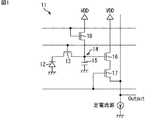
つまり、図1に示すように画素11は構成されており、画素11において、PD12で発生した電荷は、転送トランジスタ13の駆動に従ってFD14に転送され、FD14が有する容量15において蓄積される。そして、FD14に蓄積された電荷は、増幅トランジスタ16により電圧に変換され、選択トランジスタ17の駆動に従って垂直信号線に出力される。垂直信号線は、定電圧でバイアスされたトランジスタ(定電流源)に接続されており、このトランジスタと増幅トランジスタ16とが組み合わされて、いわゆるソースフォロワ回路が構成されている。また、FD14に蓄積された電荷は、リセットトランジスタ18の駆動に従って定電圧源VDDに排出される。 That is, as shown in FIG. 1, the
このような構成の画素11が半導体基板上にマトリックス状に配置されて構成された固体撮像素子では、単位電子あたりの出力電圧(変換効率)は、電荷を蓄積可能なFD14の全容量成分と、ソースフォロワ回路の変調度により決定される。ここで、電荷を蓄積可能なFD14の全容量成分は、FD14が有する容量15と、FD14に接続されている各トランジスタにより生じる容量とを合算して求められる。 In the solid-state imaging device in which the
ところで、従来の固体撮像素子では、FD14が有する容量は固定されており、ダイナミックレンジや低照度時の出力電圧などが変更されない構成となっていた。そこで、ダイナミックレンジや低照度時の出力電圧などを動的に変更するために、電荷を蓄積可能なFD14の容量を変更することができる画素を備えた固体撮像素子が提案されている(特許文献1参照)。 By the way, in the conventional solid-state imaging device, the capacity of the
図2は、電荷を蓄積可能なFD14’の容量を変更することができる画素の平面的な構造を模式的に示した図である。FIG. 2 is a diagram schematically showing a planar structure of a pixel capable of changing the capacitance of the
画素11’は、PD12が、転送トランジスタ13を介してFD14’に接続され、FD14’が、増幅トランジスタ16のゲート電極に接続され、増幅トランジスタ16の両側に選択トランジスタ17およびリセットトランジスタ18が配置されて構成されている。そして、画素11’では、転送トランジスタ13およびリセットトランジスタ18の間のFD14’にスイッチング素子19が配置されている。これにより、FD14’は、FD14’が有する容量15と、スイッチング素子19を介してFD14’に接続される付加容量15’とにより電荷を蓄積することができる。 In the
このような構成の画素11’おいて、PD12で発生した電荷は、低輝度時には容量15において蓄積され、高輝度時には容量15および付加容量15’において蓄積されるように、スイッチング素子19の駆動が制御される。このように、電荷を蓄積可能なFD14’の全容量成分がスイッチング素子19により動的に変更されることにより、画素11’では、高ダイナミックレンジが実現される。 In the
一方、従来のCMOS型固体撮像素子では、画素の行ごとに順番で画素信号の読み出しが行われることにより画像に歪が発生してしまう。そこで、このような歪の発生を回避するために、固体撮像素子が有する全てのPDで一斉に電荷の転送を行うグローバルシャッタと呼ばれる技術が開発されている。 On the other hand, in a conventional CMOS type solid-state imaging device, image signals are distorted by reading out pixel signals in order for each row of pixels. Therefore, in order to avoid the occurrence of such distortion, a technique called global shutter has been developed in which charges are transferred all at once in all PDs included in the solid-state imaging device.
例えば、特許文献2には、配線層中に配置した薄膜トランジスタを用いてグローバルシャッタを実現する固体撮像装置が開示されている。また、非特許文献1にも、配線層中に薄膜トランジスタを配置したCMOSイメージセンサが開示されている。 For example,
しかしながら、特許文献1で開示されている画素構造では、FDが有する容量と、FDに接続される付加容量との間のスイッチング素子や、付加容量などが光電変換領域(PD)と同じシリコン基板中に作成されている。同様に、特許文献2に開示されている固体撮像装置においても、PDで発生した電荷を保持する容量素子がシリコン基板中に設けられている。この場合、光電変換領域の面積が低下してしまい、光電変換効率が低下することが懸念される。 However, in the pixel structure disclosed in
また、非特許文献1に開示されているCMOSイメージセンサにおいては、ストレージ容量素子が設けられていないため、保持できる電荷量が少なくなってしまい、ダイナミックレンジを増加することは困難であると想定される。 Further, in the CMOS image sensor disclosed in
ところで、グローバルシャッタを実現することによる歪のない画像や、ダイナミックレンジが拡張された画像などを得るために、画素内に容量素子を追加することが検討されているが、容量素子を追加することによる光電変換領域の面積の低下を回避して、より良好な画像を撮像することが求められている。 By the way, in order to obtain a distortion-free image by realizing a global shutter, an image with an extended dynamic range, etc., it has been considered to add a capacitor element in a pixel. Therefore, it is desired to capture a better image while avoiding a decrease in the area of the photoelectric conversion region due to the above.
本開示は、このような状況に鑑みてなされたものであり、より良好な画像を撮像することができるようにするものである。 This indication is made in view of such a situation, and makes it possible to picturize a better picture.
本開示の一側面の撮像素子は、画素ごとに設けられ、受光した光に応じた電荷を発生する光電変換部と、所定の容量を有し、前記光電変換部から転送されてくる電荷を蓄積する蓄積部と、前記光電変換部および前記蓄積部が形成されるシリコン基板から層間絶縁膜を介して配線層中に配置され、前記蓄積部の容量に対して付加的に前記電荷を蓄積可能な容量部と、前記光電変換部および前記蓄積部が形成されるシリコン基板から層間絶縁膜を介して配線層中に配置され、前記蓄積部および前記容量部を接続する薄膜トランジスタからなる接続部とを有する画素を備え、前記画素から信号を読み出す読み出し期間中に、前記接続部が前記蓄積部と前記容量部との接続を切り替えるように駆動することで、前記接続部により前記蓄積部および前記容量部を接続状態とした信号の読み出しと、前記接続部により前記蓄積部および前記容量部を非接続状態とした信号の読み出しとが行われ、前記蓄積部および前記容量部を接続状態とした信号の信号量を超えたときには、前記蓄積部および前記容量部を非接続状態とした信号が採用される。An imaging device according to one aspect of the present disclosure is provided for each pixel and has a photoelectric conversion unit that generates charges according to received light, and has a predetermined capacity, and accumulates charges transferred from the photoelectric conversion unit. And an accumulation portion that is disposed in a wiring layer through an interlayer insulating film from a silicon substrate on which the photoelectric conversion portion and the accumulation portion are formed, and can accumulate the electric charge in addition to the capacitance of the accumulation portion A capacitor unit; and a connection unit including a thin film transistor disposed in a wiring layer through an interlayer insulating film from a silicon substrate on which the photoelectric conversion unit and the storage unit are formed, and connecting the storage unit and the capacitor unit comprising a pixel during the readout period to read out signals from the pixels, that the connecting portion is driven to switch the connection between the storage unit and the frontKiyo amount unit, the storage unit and the frontSL by the connecting portion And reading of the amount portion connected state with the signal, said storage unit and frontKiyo amount unit disconnected the signal readout is performed by the connecting portion, connecting the storage section and frontKiyo amount unit when exceeding the amount of signal state signal, a signal obtained by said accumulating unit and frontKiyo amount unit disconnected is employed.
本開示の一側面の撮像素子の駆動方法は、画素ごとに設けられ、受光した光に応じた電荷を発生する光電変換部と、所定の容量を有し、前記光電変換部から転送されてくる電荷を蓄積する蓄積部と、前記光電変換部および前記蓄積部が形成されるシリコン基板から層間絶縁膜を介して配線層中に配置され、前記蓄積部の容量に対して付加的に前記電荷を蓄積可能な容量部と、前記光電変換部および前記蓄積部が形成されるシリコン基板から層間絶縁膜を介して配線層中に配置され、前記蓄積部および前記容量部を接続する薄膜トランジスタからなる接続部とを有する画素を備える撮像素子の駆動方法であって、前記画素から信号を読み出す読み出し期間中に、前記接続部が前記蓄積部と前記容量部との接続を切り替えるように駆動することで、前記接続部により前記蓄積部および前記容量部を接続状態とした信号の読み出しと、前記接続部により前記蓄積部および前記容量部を非接続状態とした信号の読み出しとが行われるステップを含み、前記蓄積部および前記容量部を接続状態とした信号の信号量を超えたときには、前記蓄積部および前記容量部を非接続状態とした信号が採用される。Driving the dynamic processof the imaging device of one aspect of the present disclosure is provided for each pixel, a photoelectric conversion unit that generates charges corresponding to the received light, having a predetermined capacity, it is transferred from the photoelectric conversion portion An accumulating unit for accumulating the electric charge, and the photoelectric conversion unit and the silicon substrate on which the accumulating unit is formed are arranged in a wiring layer through an interlayer insulating film, and additionally to the capacitance of the accumulating unit And a capacitor comprising a thin film transistor that is disposed in a wiring layer through an interlayer insulating film from a silicon substrate on which the photoelectric conversion unit and the storage unit are formed, and that connects the storage unit and the capacitor unit a driving method of an imaging device comprising a pixel having a part, during the readout period to read out signals from the pixels, said connecting portion is driven to switch the connection between the storage unit and the frontKiyo amount unit so Step by connecting portions and reading of the storage unit and frontKiyo amount unit connection state signal, that the reading of the signal obtained by said accumulating unit and frontKiyo amount unit disconnected by the connection portion is performed wherein the said when the storage unit and frontKiyo amount unit exceeds the signal of a connected state with the signal, a signal obtained by said accumulating unit and frontKiyo amount unit disconnected is employed.
本開示の一側面の撮像素子の製造方法は、画素ごとに設けられ、受光した光に応じた電荷を発生する光電変換部と、所定の容量を有し、前記光電変換部から転送されてくる電荷を蓄積する蓄積部と、前記光電変換部および前記蓄積部が形成されるシリコン基板から層間絶縁膜を介して配線層中に配置され、前記蓄積部の容量に対して付加的に前記電荷を蓄積可能な容量部と、前記光電変換部および前記蓄積部が形成されるシリコン基板から層間絶縁膜を介して配線層中に配置され、前記蓄積部および前記容量部を接続する薄膜トランジスタからなる接続部とを有する画素を備え、前記画素から信号を読み出す読み出し期間中に、前記接続部が前記蓄積部と前記容量部との接続を切り替えるように駆動することで、前記接続部により前記蓄積部および前記容量部を接続状態とした信号の読み出しと、前記接続部により前記蓄積部および前記容量部を非接続状態とした信号の読み出しとが行われ、前記蓄積部および前記容量部を接続状態とした信号の信号量を超えたときには、前記蓄積部および前記容量部を非接続状態とした信号が採用される撮像素子の製造方法であって、前記容量部を、前記光電変換部が形成されるシリコン基板から層間絶縁膜を介して配置される配線層中に配線を形成するのと同時に形成するステップを含む。An image sensor manufacturing method according to an aspect of the present disclosure includes a photoelectric conversion unit that is provided for each pixel and generates a charge according to received light, and has a predetermined capacity, and is transferred from the photoelectric conversion unit. An accumulation unit for accumulating charges, and a photoelectric conversion unit and a silicon substrate on which the accumulation unit is formed are disposed in a wiring layer via an interlayer insulating film, and additionally store the charges with respect to the capacitance of the accumulation unit. Capacitance portion that can be stored, and a connection portion that is arranged in a wiring layer through an interlayer insulating film from a silicon substrate on which the photoelectric conversion portion and the storage portion are formed, and that includes a thin film transistor that connects the storage portion and the capacitance portion comprising pixels having bets, during the readout period to read out signals from the pixels, that the connecting portion is driven to switch the connection between the storage unit and the frontKiyo amount unit, the storage unit by the connecting portion A signal read-out in which thepre-Kiyo amount unit to a connected state and, said storage unit and frontKiyo amount unit disconnected the signal readout is performed by the connecting portion, the storage portion and beforeKiyo when exceeding the signal amount of the amount portion connected state with the signal is a manufacturing method of an imaging device signal the storage unit and frontKiyo amount unit disconnected is employed, the capacitor portion, Forming a wiring at the same time as forming a wiring in a wiring layer disposed via an interlayer insulating film from a silicon substrate on which the photoelectric conversion portion is formed.
本開示の一側面の電子機器は、画素ごとに設けられ、受光した光に応じた電荷を発生する光電変換部と、所定の容量を有し、前記光電変換部から転送されてくる電荷を蓄積する蓄積部と前記光電変換部および前記蓄積部が形成されるシリコン基板から層間絶縁膜を介して配線層中に配置され、前記蓄積部の容量に対して付加的に前記電荷を蓄積可能な容量部と、前記光電変換部および前記蓄積部が形成されるシリコン基板から層間絶縁膜を介して配線層中に配置され、前記蓄積部および前記容量部を接続する薄膜トランジスタからなる接続部とを有する画素を備え、前記画素から信号を読み出す読み出し期間中に、前記接続部が前記蓄積部と前記容量部との接続を切り替えるように駆動することで、前記接続部により前記蓄積部および前記容量部を接続状態とした信号の読み出しと、前記接続部により前記蓄積部および前記容量部を非接続状態とした信号の読み出しとが行われ、前記蓄積部および前記容量部を接続状態とした信号の信号量を超えたときには、前記蓄積部および前記容量部を非接続状態とした信号が採用される撮像素子を有する。An electronic device according to one aspect of the present disclosure is provided for each pixel, and has a photoelectric conversion unit that generates a charge according to received light, a predetermined capacity, and accumulates a charge transferred from the photoelectric conversion unit A capacitor that is disposed in a wiring layer through an interlayer insulating film from a silicon substrate on which the photoelectric conversion unit and the storage unit are formed, and capable of storing the charge in addition to the capacitor of the storage unit And a connection portion made of a thin film transistor that is arranged in a wiring layer from the silicon substrate on which the photoelectric conversion portion and the storage portion are formed via an interlayer insulating film and connects the storage portion and the capacitor portion comprising a, during the readout period to read out signals from the pixels, that the connecting portion is driven to switch the connection between the storage unit and the frontKiyo amount unit, the storage unit and beforeKiyo by the connecting portion Part and the connection state and the signal of the read, and reading of signals unconnected to the storage unit and frontKiyo amount portion by the connecting portion is made, connecting the storage section and frontKiyo amount unit status when exceeding the signal amount of the signal has an image sensor signal the storage unit and frontKiyo amount unit disconnected is employed.
本開示の一側面においては、容量部および接続部が、光電変換部が形成されるシリコン基板から層間絶縁膜を介して配線層中に配置される配線層中に形成され、容量部は、蓄積部の容量に対して付加的に電荷を蓄積可能とされ、接続部は、蓄積部および容量部を接続する薄膜トランジスタからなる。そして、画素から信号を読み出す読み出し期間中に、接続部が蓄積部と容量部との接続を切り替えるように駆動することで、接続部により蓄積部および容量部を接続状態とした信号の読み出しと、接続部により蓄積部および容量部を非接続状態とした信号の読み出しとが行われ、蓄積部および容量部を接続状態とした信号の信号量を超えたときには、蓄積部および容量部を非接続状態とした信号が採用される。In one aspect of the present disclosure, the capacitor unit and the connection unit are formed in a wiring layer disposed in the wiring layer from the silicon substrate on which the photoelectric conversion unit is formed via the interlayer insulating film, Charges can be additionally stored with respect to the capacitance of the part, and the connection part is formed of a thin film transistor that connects the storage part and the capacity part. Then, during the readout period to read out signals from the pixels, that connection portion is driven to switch the connection between the storage unitand the capacity unit, and aBiHiroshi amount portion Oyo storage unit by the connection portion and the connection state signal and read, theBiHiroshi amount portion Oyo storage unit with the joint disconnected the signal readout is performed, when it exceeds the amount of signal accumulation unit OyoBiHiroshi amount unit connected state with the signal , signal accumulation unit OyoBiHiroshi amount unit disconnected is employed.
本開示の一側面によれば、より良好な画像を撮像することができる。 According to one aspect of the present disclosure, a better image can be taken.
以下、本技術を適用した具体的な実施の形態について、図面を参照しながら詳細に説明する。 Hereinafter, specific embodiments to which the present technology is applied will be described in detail with reference to the drawings.
図3は、本技術を適用した固体撮像素子の一実施の形態の構成例を示すブロック図である。 FIG. 3 is a block diagram illustrating a configuration example of an embodiment of a solid-state imaging device to which the present technology is applied.
図3において、固体撮像素子31は、画素アレイ部32、垂直駆動回路33、水平駆動回路34、および出力回路35を備えて構成される。 In FIG. 3, the solid-
画素アレイ部32には、複数の画素41が行列状に配置されており、それぞれの画素41は、水平信号線42により行ごとに垂直駆動回路33に接続されるとともに、垂直信号線43により列ごとに水平駆動回路34に接続されている。 A plurality of
垂直駆動回路33は、水平信号線42を介して駆動信号(例えば、転送信号TX、選択信号SEL、およびリセット信号RST)を出力して、画素アレイ部32に配置されている画素41を行ごとに駆動する。 The
水平駆動回路34は、垂直信号線43を介して画素アレイ部32の各画素41から出力される信号から、CDS(Correlated Double Sampling:相関2重サンプリング)動作により信号レベルを検出するカラム処理を行い、光電変換により画素41で発生した電子に応じた出力信号を出力回路35に出力する。 The
出力回路35は、水平駆動回路34から順次出力される出力信号を、所定のレベルの電圧値に増幅して、後段の画像処理回路などに出力する。 The
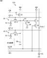
図4は、画素41の第1の構成例を示す回路図である。 FIG. 4 is a circuit diagram illustrating a first configuration example of the
図4に示すように、画素41は、PD51、転送トランジスタ52、増幅トランジスタ53、選択トランジスタ54、リセットトランジスタ55、および薄膜トランジスタ56を備えて構成される。また、転送トランジスタ52と増幅トランジスタ53との接続点がFD57を構成しており、FD57は、FD57が有する容量58と、薄膜トランジスタ56を介して接続される付加容量59とにより電子を蓄積することができる。 As shown in FIG. 4, the
PD51は、シリコン基板内に形成されるpn接合により構成され、入射した光を光電変換により電荷(電子または正孔)に変換して蓄積する光電変換部である。また、PD51は、アノード端子が接地されているとともに、カソード端子が転送トランジスタ52を介してFD57に接続されている。 The
転送トランジスタ52は、水平信号線42Tを介して垂直駆動回路33(図3)から供給される転送信号TXに従って駆動し、転送信号TXがパルス状にHighレベルとなるタイミングでオンとなる。そして、転送トランジスタ52がオンになると、PD51で発生した電子が転送トランジスタ52を介してFD57に転送される。 The
増幅トランジスタ53のゲート電極にFD57が接続されており、増幅トランジスタ53は、FD57に蓄積されている電子に応じたレベルの電圧、即ち、光電変換によりPD51で発生してFD57に転送された電子に応じたレベルの電圧を出力する。 The
選択トランジスタ54は、水平信号線42Sを介して垂直駆動回路33から供給される選択信号SELに従って駆動し、選択信号SELがパルス状にHighレベルとなるタイミングでオンとなる。そして、選択トランジスタ54がオンになると、増幅トランジスタ53から出力される電圧が、選択トランジスタ54を介して垂直信号線43に出力可能な状態となる。 The
例えば、垂直信号線43には、複数の画素41が接続されており、ある特定のライン(行)の選択トランジスタ54をオンにすることで、所望のPD51からの信号が出力される。なお、垂直信号線43は、図3の水平駆動回路34が有する定電流源60に接続されており、増幅トランジスタ53および定電流源60からなるソースフォロワ回路により、FD57に蓄積されている電子に応じたレベルを示す信号が出力(Output)される。 For example, a plurality of
リセットトランジスタ55は、水平信号線42Rを介して垂直駆動回路33から供給されるリセット信号RSTに従って駆動し、リセット信号RSTがパルス状にHighレベルとなるタイミングでオンとなる。リセットトランジスタ55がオンになると、リセットトランジスタ55を介して、FD57に蓄積されている電子が定電圧源VDDに排出されて、FD57がリセットされる。 The
薄膜トランジスタ56は、FD57と付加容量59との接続をオン/オフするスイッチング素子(接続部)である。薄膜トランジスタ56は、水平信号線42STRを介して垂直駆動回路33から供給される接続信号STRに従って駆動し、接続信号STRがパルス状にオンとなるタイミングで、FD57に付加容量59を接続する。 The
FD57は、転送トランジスタ52を介してPD51から転送されてくる電子を蓄積する。例えば、薄膜トランジスタ56がオフである場合、FD57は、FD57が有する容量58において電子を蓄積する。一方、薄膜トランジスタ56がオンである場合、FD57は、FD57が有する容量58、および、薄膜トランジスタ56を介して接続される付加容量59において電子を蓄積する。 The
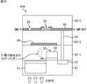
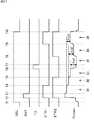
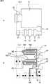
次に、図5を参照して、画素41の構造について説明する。図5Aには、画素41のFD57の近傍における断面的な構成例が示されており、図5Bには、画素41の配線層における平面的な構成例が示されている。 Next, the structure of the
また、図5に示されている画素41は、いわゆる裏面照射型の固体撮像素子の構造を採用することで、光電変換領域に入射する光量を減少することなく層間絶縁膜中に薄膜トランジスタ56および付加容量59が配置される構成となっている。なお、裏面照射型の固体撮像素子の構造については、例えば、本願出願人が出願した特許3759435号に詳細に開示されている。 Further, the
画素41は、図5Aにおいて下側を向くシリコン基板61の裏面に対して入射光が入射され、その裏面に対して反対側を向く面が表面とされる。そして、シリコン基板61の表面に層間絶縁膜62−1が積層され、層間絶縁膜62−1に層間絶縁膜62−2が積層されており、層間絶縁膜62−1および62−2の間に配線層が形成されている。 In the
PD51は、例えば、P型のシリコン基板61の内部に形成されるN型領域により構成され、転送トランジスタ52のゲート電極63が、PD51に隣接するようにシリコン基板61の表面に絶縁層64を介して配置されている。また、PD51に対して転送トランジスタ52を挟んで離間する位置のシリコン基板61内の表面部分に形成されるN型領域によりFD57が構成される。 The
FD57は、層間絶縁膜62−1を貫通するように形成されたコンタクトビア65を介して、層間絶縁膜62−1および62−2の間に形成された配線層のメタル配線66に接続されている。 The
メタル配線66の一端は、増幅トランジスタ53およびリセットトランジスタ55に接続されており、メタル配線66の他端は、配線層に形成された薄膜トランジスタ56の一端に接続されている。そして、薄膜トランジスタ56の他端に付加容量59の一方の電極59Aが接続されており、付加容量59の他方の電極59Bは接地(GND)されている。なお、付加容量59の他方の電極59Bは定電圧源VDDに接続されていてもよい。 One end of the
ここで、図5Bに示すように、付加容量59を構成する1対の電極59Aおよび59Bは、いわゆる櫛形状をしており、櫛の歯に対応する配線部分が、互いに所定の間隔を有するように交互に配置されている。この櫛の歯に対応する配線部分が、電子を蓄積する容量として機能する。また、付加容量59は、ある一定の面積を有して形成され、平面的に見たときに、PD51と重なり合う領域に形成されている。 Here, as shown in FIG. 5B, the pair of
このように画素41は構成されており、薄膜トランジスタ56が垂直駆動回路33の制御に従って駆動することにより、FD57と付加容量59との接続がオン/オフされる。例えば、垂直駆動回路33は、入射光の光量に応じて薄膜トランジスタ56のオン/オフを制御する。 Thus, the
また、画素41では、図5に示すように、薄膜トランジスタ56および付加容量59が、PD51が形成されるシリコン基板61中ではなく、シリコン基板61から層間絶縁膜62−1を介して配置される配線層中に形成される。これにより、例えば、シリコン基板61中にスイッチング素子や付加容量などを形成するような構造よりも、PD51の面積を広くとることができ、そのような構造においてPD51の光電変換効率が低下するようなことを回避することができる。なお、付加容量の一部にメタル配線などを使用している構成例においても、スイッチング素子やメタル配線部分などへのコンタクトが残っている場合には、PD51の面積が低下してしまうが、画素41では、PD51の面積の低下が回避されている。 In the
さらに、画素41では、上述したように裏面照射型の固体撮像素子の構造を採用し、配線層のメタル配線66を用いてPD51と重なるように配線層に付加容量59を形成することにより、容量の確保と工数の削減とを同時に実現することができる。 Further, the
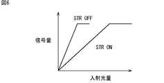
図6には、入射光量と信号量との関係が示されている。 FIG. 6 shows the relationship between the incident light amount and the signal amount.
例えば、FD57は、薄膜トランジスタ56がオフである場合には、FD57が有する容量58において電子を蓄積する。また、FD57は、薄膜トランジスタ56がオンである場合には、FD57が有する容量58と薄膜トランジスタ56を介して接続される付加容量59とにおいて電子を蓄積する。そして、FD57において電子を蓄積可能な容量が少ない場合には、FD57において電子を蓄積可能な容量が多い場合と比較して、入射光量に対する出力信号の信号量の傾斜が急勾配(高ゲイン)となる。 For example, when the
従って、入射光量が少ない場合には薄膜トランジスタ56をオフにし、FD57において電子を蓄積可能な容量を小さくすることで、高ゲインで信号レベルを出力することができるようにする。一方、入射光量が多い場合には薄膜トランジスタ56をオンにし、FD57において電子を蓄積可能な容量を大きくすることで、大きな光量まで対応可能にする。 Accordingly, when the amount of incident light is small, the
次に、画素41の駆動方法について説明する。 Next, a driving method of the
図7には、第1の駆動方法による画素41の駆動タイミングの例が示されている。第1の駆動方法では、信号の読み出し期間中に薄膜トランジスタ56をオンにしておくか、オフにしておくかにより、画素41のダイナミックレンジを選択することができる。また、水平信号線42を介して供給される信号は、それぞれHighレベルおよびLowレベルのいずれかを取り得る。なお、図7に示す時刻T1から時刻T6までの期間(以下、適宜、読み出し期間と称する)の前に、PD51に、光量に応じて光電変換された電子が蓄積されているものとする。 FIG. 7 shows an example of the driving timing of the
垂直駆動回路33は、行列状に配置されている画素41の行ごとに読み出しを順次行っており、画素41に対する読み出し期間を開始する時刻T1になると、水平信号線42Sを介して選択トランジスタ54に供給する選択信号SELをHighレベルにする。これにより、画素41の信号が垂直信号線43を介して水平駆動回路34に出力することができる状態になる。 The
時刻T2において、垂直駆動回路33は、水平信号線42Rを介してリセットトランジスタ55に供給するリセット信号RSTをHighレベルにして、リセットトランジスタ55をオンにし、FD57に蓄積されている電子を排出する。 At time T2, the
時刻T3において、垂直駆動回路33は、リセット信号RSTをLowレベルにしてリセットトランジスタ55をオフにし、FD57のリセットを完了する。このとき、FD57とリセットトランジスタ55とのカップリング容量によって出力電圧が若干低下するため、出力電圧が安定した後、FD57のリセットレベルを示す信号が、検出値D1として水平駆動回路34の検出器により検出される。 At time T3, the
時刻T4において、垂直駆動回路33は、水平信号線42Tを介して転送トランジスタ52に供給する転送信号TXをHighレベルにして、転送トランジスタ52をオンにし、PD51に蓄積されている電子をFD57に転送する。 At time T4, the
時刻T5において、垂直駆動回路33は、転送信号TXをLowレベルにして転送トランジスタ52をオフにして電子の転送を完了する。その後、FD57に蓄積された電子に応じたレベルを示す信号が、検出値D2として水平駆動回路34の検出器により検出される。 At time T5, the
時刻T6において、垂直駆動回路33は、水平信号線42Sを介して選択トランジスタ54に供給する選択信号SELをLowレベルにして、画素41に対する読み出し期間が終了する。 At time T6, the
このような駆動タイミングで垂直駆動回路33は画素41を駆動し、検出値D1と検出値D2との差分を示す信号が、光電変換によりPD51で発生した電子に応じたレベルを示す出力信号として水平駆動回路34から出力される。 The
ここで、垂直駆動回路33は、画素41から信号の読み出しを開始する前に、低ゲインモードまたは高ゲインモードのいずれかを予め選択する。例えば、垂直駆動回路33は、1フレーム前に出力された信号に基づいた光量や、図示しないセンサから出力される光量などに従い、入射光の光量に応じて、低ゲインモードまたは高ゲインモードの選択を行うことができる。 Here, the
そして、垂直駆動回路33は、光量が少ない場合には高ゲインモードを選択して、水平信号線42STRを介して薄膜トランジスタ56に供給する接続信号STRをLowレベルにして、FD57が有する容量58により、電子を蓄積するように駆動する。一方、垂直駆動回路33は、光量が多い場合には低ゲインモードを選択して、水平信号線42STRを介して薄膜トランジスタ56に供給する接続信号STRを、時刻T2から時刻T6までの期間においてHighレベルにする。これにより、FD57が有する容量58と、薄膜トランジスタ56を介してFD57に接続される付加容量59とにより、電子を蓄積するように駆動する。 The
従って、固体撮像素子31では、低照度時には高ゲインモードが選択されて、高ゲインで増幅された出力信号が出力され、高照度時には低ゲインモードが選択されて、大きな光量まで対応することが可能となる。このように、FD57において電子を蓄積可能な容量を動的に変更することで、固体撮像素子31は、ダイナミックレンジを拡大することができる。さらに、低照度時でもノイズの少ない画像を得ることができ、かつ、高照度時でも適切な(オーバーフローのない)画像を得ることができる。 Therefore, in the solid-
ここで、図7を参照して説明した第1の駆動方法では、高ゲインモードまたは低ゲインモードを予め選択する必要がある。これに対し、例えば、出力信号の信号量に応じて、高ゲインモードおよび低ゲインモードのどちらを用いるのかを自動で選択する駆動方法を採用してもよい。 Here, in the first driving method described with reference to FIG. 7, it is necessary to previously select the high gain mode or the low gain mode. On the other hand, for example, a driving method of automatically selecting which of the high gain mode and the low gain mode is used according to the signal amount of the output signal may be employed.
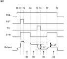
図8には、第2の駆動方法による画素41の駆動タイミングの例が示されている。 FIG. 8 shows an example of the driving timing of the
時刻T1において、垂直駆動回路33は、水平信号線42Sを介して選択トランジスタ54に供給する選択信号SELをHighレベルにする。これにより、画素41の信号が垂直信号線43を介して水平駆動回路34に出力することができる状態になる。 At time T1, the
時刻T2において、垂直駆動回路33は、水平信号線42Rを介してリセットトランジスタ55に供給するリセット信号RSTをHighレベルにするとともに、水平信号線42STRを介して薄膜トランジスタ56に供給する接続信号STRをHighレベルにする。これにより、FD57に付加容量59が接続された状態で、容量58および付加容量59に蓄積されている電子が排出され、FD57がリセットされる。 At time T2, the
時刻T3において、垂直駆動回路33は、リセット信号RSTをLowレベルにしてリセットトランジスタ55をオフにし、FD57のリセットが完了する。その後、付加容量59が接続された状態でのFD57のリセットレベルの信号が、検出値D1として水平駆動回路34の検出器により検出される。 At time T3, the
時刻T4において、垂直駆動回路33は、水平信号線42STRを介して薄膜トランジスタ56に供給する接続信号STRをLowレベルにして薄膜トランジスタ56をオフにする。その後、付加容量59が接続されない状態でのFD57のリセットレベルの信号が、検出値D2として水平駆動回路34の検出器により検出される。 At time T <b> 4, the
時刻T5において、垂直駆動回路33は、水平信号線42Tを介して転送トランジスタ52に供給する転送信号TXをHighレベルにして、転送トランジスタ52をオンにし、PD51に蓄積されている電子をFD57に転送する。 At time T5, the
時刻T6において、垂直駆動回路33は、転送信号TXをLowレベルにして転送トランジスタ52をオフにし、PD51からFD57への電子の転送を完了する。このとき、FD57には付加容量59は接続されておらず、FD57が有する容量58において、光電変換によりPD51に発生した電子が蓄積される。その後、容量58に蓄積された電子に応じたレベルの信号が、検出値D3として水平駆動回路34の検出器により検出される。 At time T6, the
時刻T7において、垂直駆動回路33は、水平信号線42STRを介して薄膜トランジスタ56に供給する接続信号STRをHighレベルにして薄膜トランジスタ56をオンにする。これにより、FD57に付加容量59が接続された状態となり、その後、容量58および付加容量59に蓄積された電子に応じたレベルの信号が、検出値D4として水平駆動回路34の検出器により検出される。 At time T7, the
時刻T8において、垂直駆動回路33は、水平信号線42STRを介して薄膜トランジスタ56に供給する接続信号STRをLowレベルにするとともに、水平信号線42Sを介して選択トランジスタ54に供給する選択信号SELをLowレベルにする。これにより、画素41に対する読み出し期間が終了する。 At time T8, the
このように、第2の駆動方法では、画素41から信号を読み出す読み出し期間中に、FD57と付加容量59との接続が切り替えられ、FD57と付加容量59とが接続された状態での信号の読み出しと、FD57と付加容量59とが接続されていない状態での信号の読み出しとが行われる。 As described above, in the second driving method, the connection between the
このような駆動により、検出値D2と検出値D3との差分を示す信号が、FD57が有する容量58においてPD51で発生した電子が蓄積されたレベルに応じた出力信号Sig1として出力される。即ち、出力信号Sig1は、高ゲインモードでの出力信号である。一方、検出値D1と検出値D4との差分を示す信号が、FD57が有する容量58とFD57に接続された付加容量59とにおいて、PD51で発生した電子が蓄積されたレベルに応じた出力信号Sig2として出力される。即ち、出力信号Sig2は、低ゲインモードでの出力信号である。 By such driving, a signal indicating a difference between the detection value D2 and the detection value D3 is output as an output signal Sig1 corresponding to the level at which electrons generated in the
例えば、高ゲインモードでの出力信号Sig1は、低ゲインモードでの出力信号Sig2に対して、より低い光量で飽和してしまうため、高ゲインモードの飽和信号量を予め求めておき、その信号量を超えたときに低ゲインモードの信号を採用することで、低光量時の感度を確保しつつ、より大きな光量にも対応することができる。 For example, since the output signal Sig1 in the high gain mode is saturated with a lower light amount than the output signal Sig2 in the low gain mode, the saturation signal amount in the high gain mode is obtained in advance, and the signal amount By adopting a signal in the low gain mode when exceeding the above, it is possible to cope with a larger light amount while ensuring sensitivity at the time of low light amount.
つまり、第2の駆動方法では、高ゲインモードでの出力信号Sig1に応じて、高ゲインモードでの出力信号Sig1と、低ゲインモードでの出力信号Sig2とのどちらを採用するのかを一意に選択することができる。これにより、低照度時には高ゲインモードを選択し、高照度時には低ゲインモードを選択する処理を自動で行うことができ、ダイナミックレンジが広い固体撮像素子31を実現することができる。 That is, in the second driving method, whether to use the output signal Sig1 in the high gain mode or the output signal Sig2 in the low gain mode is uniquely selected according to the output signal Sig1 in the high gain mode. can do. Thereby, the process of selecting the high gain mode when the illuminance is low and automatically selecting the low gain mode when the illuminance is high can be automatically performed, and the solid-
図9は、画素41の第2の構成例を示す回路図である。 FIG. 9 is a circuit diagram illustrating a second configuration example of the
図9に示すように、画素41Aは、2つの画素41−1および41−2から構成されたいわゆる2画素共有とされているが、例えば、4画素や8画素などのように共有する画素41の個数を増やしてもよい。 As shown in FIG. 9, the
画素41Aは、画素41−1および画素41−2が、増幅トランジスタ53、選択トランジスタ54、リセットトランジスタ55、およびFD57を共有するように構成されている。つまり、画素41Aは、画素41−1が有するPD51−1が、転送トランジスタ52−1を介してFD57に接続され、画素41−2が有するPD51−2が、転送トランジスタ52−2を介してFD57に接続されるように構成されている。また、画素41Aでは、図4の画素41と同様に、FD57に、薄膜トランジスタ56を介して付加容量59が接続されている。 The
図10には、第3の駆動方法による画素41Aの駆動タイミングの例が示されている。 FIG. 10 shows an example of the driving timing of the
2画素共有の構造となっている画素41Aでは、例えば、1番目の画素の読み出し期間において画素41−1から信号が読み出され、続いて、2番目の画素の読み出し期間において画素41−2から信号が読み出される。 In the
時刻T1において、垂直駆動回路33は、水平信号線42Sを介して選択トランジスタ54に供給する選択信号SELをHighレベルにする。これにより、画素41Aの信号が垂直信号線43を介して水平駆動回路34に出力することができる状態になる。 At time T1, the
時刻T2から時刻T8までが、1番目の画素の読み出し期間とされ、図8で説明した時刻T2から時刻T8までと同様に、画素41−1から信号が読み出される。つまり、時刻T5において、転送トランジスタ52−1に供給される転送信号TX1がHighレベルになって転送トランジスタ52−1がオンとなり、PD51−1に蓄積されている電子がFD57に転送される。 The period from time T2 to time T8 is the first pixel readout period, and signals are read from the pixel 41-1 in the same manner as from time T2 to time T8 described in FIG. That is, at time T5, the transfer signal TX1 supplied to the transfer transistor 52-1 goes to a high level, the transfer transistor 52-1 is turned on, and the electrons accumulated in the PD 51-1 are transferred to the
そして、時刻T4の後に検出される検出値D2−1と、時刻T6の後に検出される検出値D3−1との差分を示す信号が、FD57が有する容量58において、PD51−1で発生した電子が蓄積されたレベルに応じた出力信号Sig1−1として出力される。また、時刻T3の後に検出される検出値D1−1と、時刻T7の後に検出される検出値D4−1との差分を示す信号が、FD57が有する容量58とFD57に接続された付加容量59とにおいて、PD51−1で発生した電子が蓄積されたレベルに応じた出力信号Sig2−1として出力される。 The signal indicating the difference between the detection value D2-1 detected after time T4 and the detection value D3-1 detected after time T6 is an electron generated in the PD 51-1, in the
次に、時刻T8から時刻T14までが、2番目の画素の読み出し期間とされ、図8で説明した時刻T2から時刻T8までと同様に、画素41−2から信号が読み出される。つまり、時刻T11において、転送トランジスタ52−2に供給される転送信号TX2がHighレベルになって転送トランジスタ52−2がオンとなり、PD51−2に蓄積されている電子がFD57に転送される。 Next, the period from time T8 to time T14 is the second pixel readout period, and signals are read from the pixel 41-2 in the same manner as from time T2 to time T8 described in FIG. That is, at time T11, the transfer signal TX2 supplied to the transfer transistor 52-2 goes high, the transfer transistor 52-2 is turned on, and the electrons accumulated in the PD 51-2 are transferred to the
そして、時刻T10の後に検出される検出値D2−2と、時刻T12の後に検出される検出値D3−2との差分を示す信号が、FD57が有する容量58において、PD51−2で発生した電子が蓄積されたレベルに応じた出力信号Sig1−2として出力される。また、時刻T9の後に検出される検出値D1−2と、時刻T13の後に検出される検出値D4−2との差分を示す信号が、FD57が有する容量58とFD57に接続された付加容量59とにおいて、PD51−2で発生した電子が蓄積されたレベルに応じた出力信号Sig2−2として出力される。 The signal indicating the difference between the detection value D2-2 detected after time T10 and the detection value D3-2 detected after time T12 is the electron generated in the PD 51-2 in the
以上のように、画素41−1および41−2を画素共有するように構成された画素41Aにおいて、画素41−1から出力信号Sig1−1およびSig2−1を読み出し、画素41−2から出力信号Sig1−2およびSig2−2を読み出すことができる。また、この第3の駆動方法は、図8を参照して説明した第2の駆動方法と同様に、出力信号Sig1−1および出力信号Sig1−2に応じて、高ゲインモードと低ゲインモードとを選択する処理を自動で行うことができる。なお、図7を参照して説明した第1の駆動方法と同様に、低ゲインモードまたは高ゲインモードのいずれかを予め選択するような駆動方法を、画素41Aに適用してもよい。As described above, in the
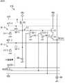
次に、図11乃至図13を参照して、画素41Aの平面的な構成例について説明する。なお、画素41Aは、図9に示した回路図では、1組の薄膜トランジスタ56および付加容量59を有した構成とされているが、図11乃至図13に示すように、同一の接続信号STRに従って駆動する2組の薄膜トランジスタ56および付加容量59を有して構成される。 Next, a planar configuration example of the
図11には、シリコン基板上のレイアウトが示されている。 FIG. 11 shows a layout on a silicon substrate.
PD51−1およびPD51−2の間に共通のFD57が配置されており、PD51−1は転送トランジスタ52−1を介してFD57に接続され、PD51−2は転送トランジスタ52−2を介してFD57に接続されている。また、FD57に隣接してリセットトランジスタ55が配置されている。そして、リセットトランジスタ55に隣接して増幅トランジスタ53が配置され、増幅トランジスタ53に隣接して選択トランジスタ54が配置されており、出力バッファとなるソースフォロワとなる。また、PD51−1およびPD51−2の間の分離領域に、ウェルコンタクト67が形成されている。 A
図12には、シリコン基板に対して第1の層間絶縁膜を介して形成される第1のメタル配線層のレイアウトが示されている。 FIG. 12 shows a layout of the first metal wiring layer formed on the silicon substrate via the first interlayer insulating film.
FD57に接続されたコンタクトビア65−1にメタル配線66が接続されている。また、メタル配線66は、増幅トランジスタ53にコンタクトビア65−2を介して接続されるとともに、薄膜トランジスタ56−1および56−2の一端に接続されている。そして、薄膜トランジスタ56−1の他端は付加容量59−1に接続され、薄膜トランジスタ56−2の他端は付加容量59−2に接続されている。A
薄膜トランジスタ56−1および付加容量59−1は、平面的に見てPD51−1に重なる領域に形成されており、薄膜トランジスタ56−2および付加容量59−2は、平面的に見てPD51−2に重なる領域に形成されている。また、付加容量59−1および59−2は、図5Bを参照して説明したように、櫛型に形成されている。 The thin film transistor 56-1 and the additional capacitor 59-1 are formed in a region overlapping the PD 51-1 in a plan view, and the thin film transistor 56-2 and the additional capacitor 59-2 are formed in the PD 51-2 in a plan view. They are formed in overlapping areas. Further, the additional capacitors 59-1 and 59-2 are formed in a comb shape as described with reference to FIG. 5B.
また、垂直信号線43を構成する出力信号配線43SIGに、選択トランジスタ54の出力(ソース電極)が接続されており、垂直信号線43を構成する接地配線43GNDに、ウェルコンタクト67が接続されている。 Further, the output (source electrode) of the
図13には、第1のメタル配線層に対して第2の層間絶縁膜を介して形成される第2のメタル配線層のレイアウトが示されている。 FIG. 13 shows the layout of the second metal wiring layer formed on the first metal wiring layer via the second interlayer insulating film.
第2のメタル配線層に形成されている配線68−1を介して、付加容量59−1の一方の電極が接地配線43GNDに接続されており、配線68−2を介して、付加容量59−2の一方の電極が接地配線43GNDに接続されている。 One electrode of the additional capacitor 59-1 is connected to the ground wiring 43GND through the wiring 68-1 formed in the second metal wiring layer, and the additional capacitor 59- is connected through the wiring 68-2. One of the two electrodes is connected to the ground wiring 43GND.
また、第2のメタル配線層には、水平信号線42STR−1および42STR−2、水平信号線42T−1および42T−2、水平信号線42S、並びに水平信号線42Rが形成されている。水平信号線42STR−1および42STR−2は、薄膜トランジスタ56−1および56−2にそれぞれ接続されており、水平信号線42T−1および42T−2は、転送トランジスタ52−1および52−2にそれぞれ接続されている。また、水平信号線42Sは、選択トランジスタ54に接続されており、水平信号線42Rは、リセットトランジスタ55に接続されている。 In the second metal wiring layer, horizontal signal lines 42STR-1 and 42STR-2,
以上のようなレイアウトで、画素41−1および41−2による2画素共有構造の画素41Aを構成することができる。また、増幅トランジスタ53、選択トランジスタ54、リセットトランジスタ55、およびFD57を共有することにより、PD51−1および51−2の面積を広くすることができ、光電変換効率を向上させることができる。 With the layout as described above, the
なお、図11乃至図13に示したレイアウトは、本実施の形態における機能を実現する一例であり、同様の機能を実現可能な様々なレイアウトを採用することができる。 Note that the layouts shown in FIGS. 11 to 13 are examples for realizing the functions in this embodiment, and various layouts that can realize the same functions can be employed.
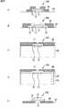
次に、図14は、画素41の第3の構成例を示す断面図である。 Next, FIG. 14 is a cross-sectional view illustrating a third configuration example of the
図14に示すように、画素41Bは、シリコン基板61の表面に層間絶縁膜62−1乃至62−3が積層されており、層間絶縁膜62−1および62−2の間に第1の配線層が形成され、層間絶縁膜62−2および62−3の間に第2の配線層が形成されている。そして、画素41Bでは、薄膜トランジスタ56および付加容量59が第2の配線層に形成されており、シリコン基板61と第2の配線層との間の第1の配線層に遮光膜69が形成されている。遮光膜69は、第1の配線層のメタルを使用して、シリコン基板61側から見て薄膜トランジスタ56を覆うように配置される。 As shown in FIG. 14, in the
このように、画素41Bでは、遮光膜69を形成することにより、裏面から入射された光のうち、シリコン基板61で吸収されなかった光を遮光膜69で遮光することができる。例えば、シリコン基板61で吸収されなかった光が薄膜トランジスタ56に到達する場合には、バンドギャップが狭い半導体層を使用していると、薄膜トランジスタ56での光電変換によってリーク電流が発生する恐れがある。 In this manner, in the
これに対し、画素41Bでは、薄膜トランジスタ56よりもシリコン基板61側に遮光膜69を形成することにより、上述したようなリーク電流の発生を防止することができる。これにより、よりノイズの少ない固体撮像素子31を実現することができる。 In contrast, in the
次に、図15は、画素41の第4の構成例を示す図である。図15Aには、画素41CのFD57の近傍における断面的な構成例が示されており、図15Bには、画素41Cの配線層における平面的な構成例が示されている。 Next, FIG. 15 is a diagram illustrating a fourth configuration example of the
画素41Cは、積層型の付加容量59’を備えて構成される。即ち、画素41Cにおいて、付加容量59’は、平面形状に形成された1対の電極59A’および59B’の間に、絶縁膜59Cが挟み込まれて構成される。 The pixel 41C includes a stacked additional capacitor 59 '. That is, in the pixel 41C, the additional capacitor 59 'is configured by sandwiching the insulating
このように、画素41Cでは、積層型の付加容量59’を採用することにより、櫛型の付加容量59を採用した場合よりも、より大容量化を図ることができる。これにより、画素41Cは、より大きな光量まで対応することができる。 In this manner, in the pixel 41C, by using the stacked additional capacitor 59 ', it is possible to achieve a larger capacity than when the comb-shaped
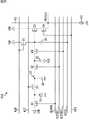
次に、図16は、画素41の第5の構成例を示す回路図である。 Next, FIG. 16 is a circuit diagram illustrating a fifth configuration example of the
図16に示すように、画素41Dは、PD51、転送トランジスタ52、増幅トランジスタ53、選択トランジスタ54、リセットトランジスタ55を備える点で、図4の画素41と共通する。但し、画素41Dは、薄膜トランジスタ56−1および56−2、並びに、付加容量59−1および59−2を備える点で、図4の画素41と異なる構成となっている。 As shown in FIG. 16, the
画素41Dでは、薄膜トランジスタ56−1が水平信号線42STR−1に接続されており、薄膜トランジスタ56−2が水平信号線42STR−2に接続されており、薄膜トランジスタ56−1および56−2は、それぞれ独立して駆動する。 In the
このように構成されている画素41Dでは、光電変換によりPD51で発生した電子が、容量58に蓄積され、容量58および付加容量59−1に蓄積され、または、容量58と付加容量59−1および59−2に蓄積されるように、電子を蓄積可能なFD57の容量を変更することができる。 In the
次に、図17には、第4の駆動方法による画素41Dの駆動タイミングの例が示されている。 Next, FIG. 17 shows an example of the driving timing of the
時刻T1において、垂直駆動回路33は、水平信号線42Sを介して選択トランジスタ54に供給する選択信号SELをHighレベルにする。これにより、画素41Dの信号が垂直信号線43を介して水平駆動回路34に出力することができる状態になる。 At time T1, the
時刻T2において、垂直駆動回路33は、水平信号線42Rを介してリセットトランジスタ55に供給するリセット信号RSTをHighレベルにする。また、このとき、垂直駆動回路33は、水平信号線42STR−1を介して薄膜トランジスタ56−1に供給する接続信号STR1をHighレベルにするとともに、水平信号線42STR−2を介して薄膜トランジスタ56−2に供給する接続信号STR2をHighレベルにする。これにより、FD57が有する容量58と、薄膜トランジスタ56−1および56−2を介してFD57に接続される付加容量59−1および59−2とがリセットされる。 At time T2, the
時刻T3において、垂直駆動回路33は、リセット信号RSTをLowレベルにしてリセットトランジスタ55をオフにし、FD57のリセットが完了する。その後、FD57が有する容量58に、付加容量59−1および59−2が接続された状態でのFD57のリセットレベルの信号が、検出値D1として水平駆動回路34の検出器により検出される。 At time T3, the
時刻T4において、垂直駆動回路33は、水平信号線42STR−1を介して薄膜トランジスタ56−1に供給する接続信号STR1をLowレベルにして薄膜トランジスタ56−1をオフにする。その後、FD57が有する容量58に付加容量59−2が接続された状態でのFD57のリセットレベルの信号が、検出値D2として水平駆動回路34の検出器により検出される。 At time T4, the
時刻T5において、垂直駆動回路33は、水平信号線42STR−2を介して薄膜トランジスタ56−2に供給する接続信号STR2をLowレベルにして薄膜トランジスタ56−2をオフにする。その後、容量58だけの状態でのFD57のリセットレベルの信号が、検出値D3として水平駆動回路34の検出器により検出される。 At time T5, the
時刻T6において、垂直駆動回路33は、水平信号線42Tを介して転送トランジスタ52に供給する転送信号TXをHighレベルにして、転送トランジスタ52をオンにし、PD51に蓄積されている電子をFD57に転送する。 At time T6, the
時刻T7において、垂直駆動回路33は、転送信号TXをLowレベルにして転送トランジスタ52をオフにし、PD51からFD57への電子の転送を完了する。その後、容量58だけが接続された状態でFD57に蓄積された電子に応じたレベルの信号が、検出値D4として水平駆動回路34の検出器により検出される。 At time T7, the
時刻T8において、垂直駆動回路33は、水平信号線42STR−2を介して薄膜トランジスタ56−2に供給する接続信号STR2をHighレベルにして薄膜トランジスタ56−2をオンにする。その後、容量58に付加容量59−2が接続された状態でFD57に蓄積された電子に応じたレベルの信号が、検出値D5として水平駆動回路34の検出器により検出される。 At time T8, the
時刻T9において、垂直駆動回路33は、水平信号線42STR−1を介して薄膜トランジスタ56−1に供給する接続信号STR1をHighレベルにして薄膜トランジスタ56−1をオンにする。その後、容量58に付加容量59−1および59−2が接続された状態でFD57に蓄積された電子に応じたレベルの信号が、検出値D6として水平駆動回路34の検出器により検出される。 At time T9, the
時刻T10において、垂直駆動回路33は、水平信号線42STR−1および42STR−2を介して薄膜トランジスタ56−1および56−2に供給する接続信号STR1およびSTR2を、それぞれLowレベルにする。また、このとき、垂直駆動回路33は、水平信号線42Sを介して選択トランジスタ54に供給する選択信号SELをLowレベルにする。これにより、画素41Dに対する読み出し期間が終了する。At time T10, the
このような駆動タイミングで垂直駆動回路33は画素41Dを駆動し、検出値D3と検出値D4との差分を示す信号が、FD57が有する容量58においてPD51で発生した電子が蓄積されたレベルに応じた出力信号Sig1として出力される。また、検出値D2と検出値D5との差分を示す信号が、容量58に付加容量59−2が接続された状態のFD57においてPD51で発生した電子が蓄積されたレベルに応じた出力信号Sig2として出力される。また、検出値D1と検出値D6との差分を示す信号が、容量58に付加容量59−1および59−2が接続された状態のFD57においてPD51で発生した電子が蓄積されたレベルに応じた出力信号Sig3として出力される。 At such drive timing, the
以上のように、画素41Dでは、光電変換によりPD51で発生した電子が、それぞれ異なる3種類の容量からなるFD57において出力信号に変換されるので、照射される光量に適したゲインで変換することができる。 As described above, in the
次に、図18は、画素41の第6の構成例を示す回路図である。 Next, FIG. 18 is a circuit diagram illustrating a sixth configuration example of the
図18に示すように、画素41Eは、2画素共有の構成となっている点で、図9の画素41Aと共通する。但し、画素41Eは、薄膜トランジスタ56−1および56−2、並びに、付加容量59−1および59−2を備え、薄膜トランジスタ56−1および56−2は、それぞれ独立して駆動する点で、図9の画素41Aと異なる構成となっている。 As shown in FIG. 18, the
次に、図19には、第5の駆動方法による画素41Eの駆動タイミングの例が示されている。 Next, FIG. 19 shows an example of the driving timing of the
2画素共有の構造となっている画素41Eでは、例えば、1番目の画素の読み出し期間において画素41−1から信号が読み出され、続いて、2番目の画素の読み出し期間において画素41−2から信号が読み出される。 In the
時刻T1において、垂直駆動回路33は、水平信号線42Sを介して選択トランジスタ54に供給する選択信号SELをHighレベルにする。これにより、画素41Eの信号が垂直信号線43を介して水平駆動回路34に出力することができる状態になる。 At time T1, the
時刻T2から時刻T10までが、1番目の画素の読み出し期間とされ、図17で説明した時刻T2から時刻T10までと同様に、画素41−1から信号が読み出される。つまり、時刻T6において、転送トランジスタ52−1に供給される転送信号TX1がHighレベルになって転送トランジスタ52−1がオンとなり、PD51−1に蓄積されている電子がFD57に転送される。 The period from time T2 to time T10 is the readout period of the first pixel, and signals are read from the pixel 41-1 in the same manner as from time T2 to time T10 described in FIG. That is, at time T6, the transfer signal TX1 supplied to the transfer transistor 52-1 goes to a high level, the transfer transistor 52-1 is turned on, and the electrons accumulated in the PD 51-1 are transferred to the
そして、時刻T5の後に検出される検出値D3−1と、時刻T7の後に検出される検出値D4−1との差分を示す信号が、FD57が有する容量58においてPD51−1で発生した電子が蓄積されたレベルに応じた出力信号Sig1−1として出力される。また、時刻T4の後に検出される検出値D2−1と、時刻T8の後に検出される検出値D5−1との差分を示す信号が、容量58に付加容量59−2が接続された状態のFD57においてPD51−1で発生した電子が蓄積されたレベルに応じた出力信号Sig2−1として出力される。また、時刻T3の後に検出される検出値D1−1と、時刻T9の後に検出される検出値D6−1との差分を示す信号が、容量58に付加容量59−1および59−2が接続された状態のFD57においてPD51−1で発生した電子が蓄積された出力信号Sig3−1として出力される。 Then, a signal indicating a difference between the detection value D3-1 detected after time T5 and the detection value D4-1 detected after time T7 indicates that electrons generated in the PD 51-1 in the
次に、時刻T10から時刻T18までが、2番目の画素の読み出し期間とされ、図17で説明した時刻T2から時刻T10までと同様に、画素41−2から信号が読み出される。つまり、時刻T14において、転送トランジスタ52−2に供給される転送信号TX2がHighレベルになって転送トランジスタ52−2がオンとなり、PD51−2に蓄積されている電子がFD57に転送される。 Next, the period from time T10 to time T18 is the second pixel readout period, and signals are read from the pixel 41-2 in the same manner as from time T2 to time T10 described in FIG. That is, at time T <b> 14, the transfer signal TX <b> 2 supplied to the transfer transistor 52-2 becomes high level, the transfer transistor 52-2 is turned on, and the electrons accumulated in the PD 51-2 are transferred to the
そして、時刻T13の後に検出される検出値D3−2と、時刻T15の後に検出される検出値D4−2との差分を示す信号が、FD57が有する容量58においてPD51−2で発生した電子が蓄積されたレベルに応じた出力信号Sig1−2として出力される。また、時刻T12の後に検出される検出値D2−2と、時刻T16の後に検出される検出値D5−2との差分を示す信号が、容量58に付加容量59−2が接続された状態のFD57においてPD51−2で発生した電子が蓄積されたレベルに応じた出力信号Sig2−2として出力される。また、時刻T11の後に検出される検出値D1−2と、時刻T17の後に検出される検出値D6−2との差分を示す信号が、容量58に付加容量59−1および59−2が接続された状態のFD57においてPD51−2で発生した電子が蓄積された出力信号Sig3−2として出力される。 A signal indicating a difference between the detection value D3-2 detected after the time T13 and the detection value D4-2 detected after the time T15 indicates that electrons generated in the PD 51-2 in the
以上のように、2画素共有の構成とされる画素41Eにおいて、光電変換によりPD51−1および51−2で発生した電子が、それぞれ異なる3種類の容量からなるFD57において出力信号に変換されるので、照射される光量に適したゲインで変換することができる。 As described above, in the
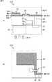
次に、図20を参照して、画素41で採用される薄膜トランジスタ56の各種の構成例について説明する。薄膜トランジスタ56については、さまざまな材料、構造のものが利用可能である。 Next, various configuration examples of the
図20Aには、逆スタガー構造の薄膜トランジスタ56Aが示されている。薄膜トランジスタ56Aは、層間絶縁膜62の表面に、まず、金属からなるゲート電極71を形成し、ゲート絶縁膜72を形成した後、半導体層73を作成する。次に、ソース/ドレイン電極となる金属層をメタル配線66で形成し、逆スタガー構造の薄膜トランジスタ56Aが完成する。 FIG. 20A shows a
ゲート電極71およびメタル配線66は、例えばAl、Cu、Ti、Mo、W、Crや、それらの窒化物、酸化物、ITO、ZnOなどの透明金属、あるいはこれらのうちの複数の金属の積層構造が利用可能である。またゲート絶縁膜72としてはSi酸化物、Si窒化物、Hf酸化物、Al酸化物、Ta酸化物やそれらの積層構造を用いることができる。半導体層73としては、ZnO、SnO、InOやそれらにGaを添加したもの、またはこれらのうちの元素を複数含有した酸化物半導体を用いることができる。なお、半導体層73として有機薄膜を用いた構成を採用することで、塗布により容易に製造することができる。 The
図20Bには、半導体層73とメタル配線66との間に、コンタクト層74が挟まれた構造の薄膜トランジスタ56Bが示されている。コンタクト層の材料としては、導電率を向上させた酸化物半導体を用いることができ、例えば、In−Ga−Zn−O系、In−Sn−Zn−O系、Ga−Sn−Zn−O系、In−Zn−O系、Sn−Zn−O系、In−Sn−O系、Ga−Zn−O系、In−O系、Sn−O系またはZn−O系の酸化物半導体を用いることができる。 FIG. 20B shows a
図20Cには、ゲート電極71が層間絶縁膜62に埋め込まれた構造の薄膜トランジスタ56Cが示されている。 FIG. 20C shows a
図20Dには、ゲート電極71が層間絶縁膜62に埋め込まれ、ゲート電極71および層間絶縁膜62の全面にゲート絶縁膜72が残されるような構造の薄膜トランジスタ56Dが示されている。 FIG. 20D shows a
図20Eには、スタガー構造の薄膜トランジスタ56Eが示されており、薄膜トランジスタ56Eとして、薄膜トランジスタ56A乃至56Dのような逆スタガー構造ではなく、スタガー構造を採用することができる。 FIG. 20E illustrates a
次に、図21を参照して、固体撮像素子31の製造方法について説明する。 Next, a method for manufacturing the solid-
まず、第1の工程において、例えば、イオン注入法などにより、シリコン基板61の内部にPD51およびFD57を形成する。 First, in the first step, the
次に、第2の工程において、シリコン基板61の表面に、絶縁層64を介して転送トランジスタ52のゲート電極63を形成し、層間絶縁膜62−1を積層した後に、コンタクトビア65を形成してFD57に接続する。 Next, in the second step, the
そして、第3の工程において、薄膜トランジスタ56(図20のゲート電極71、ゲート絶縁膜72、および半導体層73)を形成した後に、メタル配線66を形成するのと同時に、櫛形状の付加容量59を形成する。 Then, in the third step, after forming the thin film transistor 56 (the
その後、第4の工程において、層間絶縁膜62−2を積層することにより、画素41が形成された固体撮像素子31を製造することができる。 Thereafter, in the fourth step, the solid-
以上のように、固体撮像素子31の製造方法では、メタル配線66を形成するのと同時に、櫛形状の付加容量59を形成することができ、従来の製造方法から付加容量59を形成するためだけに工程を増やすことはなく、固体撮像素子31を製造することができる。なお、以下で説明する構成例の画素41を有する固体撮像素子31も同様の製造方法により製造することができる。 As described above, in the manufacturing method of the solid-
次に、図22乃至図31を参照し、グローバルシャッタの機能を有する固体撮像素子31に採用される画素41の構成例について説明する。 Next, a configuration example of the
つまり、図5に示したような、層間絶縁膜62−1および62−2の間に付加容量59が形成されている画素41の構造を応用して、全ての画素41の露光タイミングを揃えて、一括読み出しを行う、いわゆるグローバルシャッタ機能を有する固体撮像素子31を実現することができる。 In other words, by applying the structure of the
図22は、画素41の第7の構成例を示す回路図である。 FIG. 22 is a circuit diagram illustrating a seventh configuration example of the
図22に示すように、画素41Fは、PD51、転送トランジスタ52、増幅トランジスタ53、選択トランジスタ54、リセットトランジスタ55、FD57、容量58、排出トランジスタ81、薄膜トランジスタ82、および容量83を備えて構成される。 As shown in FIG. 22, the
画素41Fでは、PD51のアノード端子が接地され、PD51のカソード端子が、転送トランジスタ52を介してFD57に接続されるとともに、排出トランジスタ81を介して定電圧源VDDに接続されている。また、FD57は、容量58を介して接地され、リセットトランジスタ55を介して定電圧源VDDに接続され、薄膜トランジスタ82を介して増幅トランジスタ53のゲート電極に接続されている。そして、薄膜トランジスタ82と増幅トランジスタ53のゲート電極との接続点は、容量83を介して電源VCSに接続されている。また、増幅トランジスタ53は、一方の端子が定電圧源VDDに接続されるとともに、他方の端子が、選択トランジスタ54を介して、定電流源60が接続された垂直信号線43に接続されている。 In the
また、転送トランジスタ52のゲート電極には水平信号線42Tが接続され、選択トランジスタ54のゲート電極には水平信号線42Sが接続され、リセットトランジスタ55のゲート電極には水平信号線42Rが接続されている。さらに、排出トランジスタ81のゲート電極には水平信号線42ABGが接続され、薄膜トランジスタ82のゲート電極には水平信号線42STRが接続されている。 Further, the
つまり、画素41Fでは、FD57と増幅トランジスタ53との間の接続を切り替える薄膜トランジスタ82(スイッチング素子)が接続され、薄膜トランジスタ82と増幅トランジスタ53との接続点に容量83の一方の端子が接続され、容量83の他方の端子に電源VCSが接続されている点で、図4の画素41の異なる構成とされている。また、画素41Fでは、PD51に蓄積された電子を排出するために、排出トランジスタ81が設けられている点でも、図4の画素41の異なる構成とされている。 That is, in the
このように画素41Fは構成されており、複数の画素41Fが画素アレイ部32に行列状に配置された固体撮像素子31では、グローバルシャッタの機能を実現するために、全ての画素41Fにおいて、PD51からFD57へ同時に電子が転送される。その後、薄膜トランジスタ82を介してFD57から容量83に電子が転送され、容量83において電子が保持される。そして、画素信号の読み出し対象となった画素41Fでは、容量83に蓄積されている電子に応じたレベルの信号、即ち、光電変換によりPD51で発生してFD57に転送された後に容量83に転送された電子に応じたレベルの信号が出力される。 In this way, the
次に、図23を参照して、画素41Fの構造について説明する。図23Aには、画素41FのFD57の近傍における断面的な構成例が示されており、図23Bには、画素41Fの配線層における平面的な構成例が示されている。なお、図23では、図5の画素41と共通する構成について同一の符号を付しており、その詳細な説明については省略する。 Next, the structure of the
画素41Fは、図5の画素41と同様に、シリコン基板61に層間絶縁膜62−1および62−2が積層され、層間絶縁膜62−1および62−2の間に配線層が形成されて構成されている。また、その配線層に形成される容量83は、図5を参照して説明した付加容量59と同様に、櫛形状をしている。但し、図22に示したように、画素41Fでは、薄膜トランジスタ82を介してFD57および増幅トランジスタ53が接続される点で、画素41と異なる構成とされている。 Similarly to the
即ち、FD57は、コンタクトビア65を介して、層間絶縁膜62−1および62−2の間に形成された配線層のメタル配線66に接続され、メタル配線66の一端は、リセットトランジスタ55に接続されている。また、メタル配線66の他端は、配線層に形成された薄膜トランジスタ82の一端に接続されており、薄膜トランジスタ82の他端に、容量83を構成する一方の電極83Aが接続されている。さらに、電極83Aは、増幅トランジスタ53に接続されており、容量83を構成する他方の電極83Bは、電源VCSに接続されている。 That is, the
ここで、図23Bに示すように、容量83を構成する1対の電極83Aおよび83Bは、いわゆる櫛形状をしており、櫛の歯に対応する配線部分が、互いに所定の間隔を有するように交互に配置されている。この櫛の歯に対応する配線部分が、電子を蓄積する容量として機能する。また、容量83は、ある一定の面積を有して形成され、平面的に見たときに、PD51と重なり合う領域に形成されている。 Here, as shown in FIG. 23B, the pair of
このように画素41Fは構成されており、薄膜トランジスタ82が垂直駆動回路33の制御に従って駆動することにより、FD57と容量83との接続がオン/オフされる。例えば、PD51からFD57に電子が転送された後、薄膜トランジスタ82がオンとなり、FD57に蓄積されている電子が、容量83に転送される。なお、このとき、電極83Bに接続される電源VCSがHighレベルの状態とされることで、電極83Aの電圧が上昇し、FD57に蓄積されている電子を容量83に転送することが可能となる。なお、電源VCSのHighレベルの電圧は、0Vから定電圧源VDDまでの間の適当な値とすることができる。 Thus, the
このように、画素41Fでは、グローバルシャッタの機能を有する固体撮像素子31において、全ての画素41Fで同時にPD51から転送された電子を保持する容量83が、シリコン基板61から層間絶縁膜62−1を介して配置される配線層中に形成される。また、薄膜トランジスタ82も、容量83と同じ配線層中に形成される。このように、薄膜トランジスタ82および容量83が配線層中に形成されることで、それらがシリコン基板61中に形成されるような構造よりも、PD51の面積を広くとることができる。従って、そのような構造においてPD51の光電変換効率が低下するようなことを回避することができる。 As described above, in the
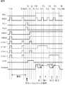
図24には、第6の駆動方法による画素41Fの駆動タイミングの例が示されている。第6の駆動方法は、グローバルシャッタ動作における読み出し方法であり、各信号は、HighレベルおよびLowレベルの2値を取り得る。 FIG. 24 shows an example of the driving timing of the
まず、時刻T1において、垂直駆動回路33は、全ての行の画素41Fに対して同時に、PD51、FD57、および容量83のリセットを行うために、リセット信号RST、接続信号STR、および排出信号ABGをHighレベルにする。 First, at time T1, the
接続信号STRは、水平信号線42STRを介して薄膜トランジスタ82に供給され、接続信号STRがHighレベルになると薄膜トランジスタ82がオンになり、FD57と容量83とが接続される。リセット信号RSTは、水平信号線42Rを介してリセットトランジスタ55に供給され、リセット信号RSTがHighレベルになるとリセットトランジスタ55がオンになり、FD57および容量83がリセットされる。また、排出信号ABGは、水平信号線42ABGを介して排出トランジスタ81に供給され、排出信号ABGがHighレベルになると排出トランジスタ81がオンになり、PD51に蓄積されている電子が定電圧源VDDに排出される。 The connection signal STR is supplied to the
時刻T2において、垂直駆動回路33は、全ての行の画素41Fに対して同時に、リセット信号RST、接続信号STR、および排出信号ABGをLowレベルにして、リセットトランジスタ55、薄膜トランジスタ82、および排出トランジスタ81がオフになる。これにより、PD51、FD57、および容量83のリセットが完了し、全ての行の画素41Fにおいて同時に、PD51の露光が開始される。 At time T2, the
時刻T3において、垂直駆動回路33は、全ての行の画素41Fに対して同時に、リセット信号RSTおよび接続信号STRをHighレベルにして、時刻T4において、リセット信号RSTおよび接続信号STRをLowレベルにする。これにより、リセットトランジスタ55および薄膜トランジスタ82がオンになり、露光期間中に主にFD57でリークによって生成された電子が、FD57および容量83から排出される。 At time T3, the
時刻T5において、垂直駆動回路33は、全ての行の画素41Fに対して同時に、水平信号線42Tを介して転送トランジスタ52に供給する転送信号TXをHighレベルにして、転送トランジスタ52をオンにする。これにより、画素41Fの露光が終了し、全ての行の画素41Fにおいて同時に、PD51に蓄積されている電子がFD57に転送される。この転送動作が、全ての画素41Fで同時に行われることにより、グローバルシャッタ動作が実現される。 At time T5, the
時刻T6において、垂直駆動回路33は、全ての行の画素41Fに対して同時に、転送信号TXをLowレベルにして転送トランジスタ52をオフにして電子の転送を完了する。 At time T6, the
時刻T7において、垂直駆動回路33は、全ての行の画素41Fに対して同時に、水平信号線42STRを介して薄膜トランジスタ82に供給する接続信号STRをHighレベルにし、薄膜トランジスタ82を介してFD57および容量83を接続する。このとき、垂直駆動回路33は、薄膜トランジスタ82と接続される端子に対して反対側となる容量83の端子(図23の電極83B)に接続されている電源VCSの電位を、時刻T6から時刻T9までの間においてHighレベルにする。これにより、FD57から容量83へ電子が転送されるようにポテンシャルが形成され、FD57に蓄積されている電子を容量83に転送することができる。 At time T7, the
また、時刻T7において、垂直駆動回路33は、全ての行の画素41Fに対して同時に、水平信号線42ABGを介して排出トランジスタ81に供給される排出信号ABGをHighレベルにする。排出信号ABGは、時刻T7以降においてHighレベルが維持され、PD51において光電変換により発生する電子が定電圧源VDDに排出され続けることで、PD51に余分な電子が蓄積されないようにする。 At time T7, the
時刻T8において、垂直駆動回路33は、全ての行の画素41Fに対して同時に、水平信号線42STRを介して薄膜トランジスタ82に供給する接続信号STRをLowレベルにして、FD57から容量83への電子の転送を完了する。 At time T8, the
ここで、時刻T1から時刻T8までの動作は、全ての画素41Fで同じタイミングで行われ、全ての画素41FのPD51において発生した電子が容量83に蓄積されており、その後、画素41Fの行ごとに順次、信号の読み出しが行われる。例えば、時刻T9から時刻12までが1行目の画素41Fの読み出し期間とされ、時刻T13から時刻T16までが2行目の画素41Fの読み出し期間とされる。そして、以下同様に、最終行まで順次、読み出し期間とされた行の画素41Fの信号の読み出しが行われる。Here, the operation from time T1 to time T8 is performed at the same timing in all the
時刻T9において、垂直駆動回路33は、1行目の画素41Fに対して、水平信号線42Sを介して選択トランジスタ54に供給する選択信号SELをHighレベルにし、画素41Fの信号が垂直信号線43を介して水平駆動回路34に出力することができる状態にする。そして、出力電圧が安定した後、容量83に蓄積された電子に応じたレベルを示す信号が、検出値D1として水平駆動回路34の検出器により検出される。 At time T9, the
時刻T10において、垂直駆動回路33は、1行目の画素41Fに対して、リセット信号RSTおよび接続信号STRをHighレベルにして、リセットトランジスタ55および薄膜トランジスタ82をオンにする。これにより、FD57および容量83に蓄積された電子が定電圧源VDDに排出されて、FD57および容量83がリセットされる。 At time T10, the
時刻T11において、垂直駆動回路33は、リセット信号RSTおよび接続信号STRをLowレベルにしてリセットトランジスタ55および薄膜トランジスタ82をオフにし、FD57および容量83のリセットを完了する。そして、出力電圧が安定した後、容量83のリセットレベルを示す信号が、検出値D2として水平駆動回路34の検出器により検出される。 At time T <b> 11, the
時刻T12において、垂直駆動回路33は、水平信号線42Sを介して選択トランジスタ54に供給する選択信号SELをLowレベルにして、1行目の画素41Fに対する読み出し期間が終了する。 At time T12, the
このように、時刻T9から時刻12までが1行目の画素41Fの読み出し期間とされ、検出値D1と検出値D2との差分を示す信号が、光電変換によりPD51で発生した電子に応じたレベルを示す出力信号Sigとして水平駆動回路34から出力される。 As described above, the period from time T9 to
その後、時刻T9から時刻12までと同様に、時刻T13から時刻16までが2行目の画素41Fの読み出し期間とされ、2行目の画素41FのPD51で発生した電子に応じたレベルを示す出力信号Sigが出力される。以下、全ての行の画素41Fについて同様の動作が繰り返され、全ての画素41Fから画素信号が出力される。 Thereafter, similarly to the time T9 to the
以上のように、画素41Fを有する固体撮像素子31において、グローバルシャッタ動作を実現することができる。 As described above, the global shutter operation can be realized in the solid-
図25は、画素41の第8の構成例を示す回路図である。 FIG. 25 is a circuit diagram illustrating an eighth configuration example of the
図25に示されている画素41Gは、リセットレベルを示す信号が読み出された後に、PD51から転送された電子に応じたレベルを示す信号を読み出して画素信号を算出する相関二重サンプリングが可能な構成である。 The
図25に示すように、画素41Gは、PD51、転送トランジスタ52、増幅トランジスタ53、選択トランジスタ54、リセットトランジスタ55、FD57、容量58、排出トランジスタ81、薄膜トランジスタ82、および容量83を備える点で、図22の画素41Fと共通する。但し、画素41Gは、薄膜トランジスタ84および容量85を備える点で、図22の画素41Fと異なる構成となっている。 As shown in FIG. 25, the
薄膜トランジスタ84および容量85は、薄膜トランジスタ82および容量83と同様に、層間絶縁膜62−1および62−2(図23)の間に形成される。 The
薄膜トランジスタ84は、薄膜トランジスタ82および容量83の接続点と、増幅トランジスタ53のゲート電極との接続を切り替えることができるように配置される。そして、薄膜トランジスタ84と増幅トランジスタ53との接続点には、容量85の一方の端子が接続されるとともに、リセットトランジスタ55を介して定電圧源VDDが接続される。また、薄膜トランジスタ82のゲート電極には水平信号線42STR1が接続され、薄膜トランジスタ84のゲート電極には水平信号線42STR2が接続され、容量85の他方の端子には水平信号線42CSが接続されている。 The
このように画素41Gは構成されており、複数の画素41Gが画素アレイ部32に行列状に配置された固体撮像素子31では、グローバルシャッタの機能を実現するために、全ての画素41Gにおいて、PD51からFD57へ同時に電子が転送される。その後、薄膜トランジスタ82を介してFD57から容量83に電子が転送され、容量83において電子が保持される。そして、画素信号の読み出し対象となった画素41Gでは、容量85のリセットレベルの信号が出力された後に、薄膜トランジスタ84を介して容量83から容量85に電子が転送されて、容量85に蓄積されている電子に応じたレベルの信号が出力される。 In this way, the
図26には、第7の駆動方法による画素41Gの駆動タイミングの例が示されている。 FIG. 26 shows an example of the driving timing of the
まず、時刻T1において、垂直駆動回路33は、全ての行の画素41Gに対して同時に、PD51、FD57、容量83、および容量85のリセットを行うために、リセット信号RST、排出信号ABG、接続信号STR1、および接続信号STR2をHighレベルにする。 First, at time T1, the
接続信号STR1は、水平信号線42STR1を介して薄膜トランジスタ82に供給され、接続信号STR1がHighレベルになると薄膜トランジスタ82がオンになり、FD57と容量83とが接続される。接続信号STR2は、水平信号線42STR2を介して薄膜トランジスタ84に供給され、接続信号STR2がHighレベルになると薄膜トランジスタ84がオンになり、容量83と容量85とが接続される。 The connection signal STR1 is supplied to the
リセット信号RSTは、水平信号線42Rを介してリセットトランジスタ55に供給され、リセット信号RSTがHighレベルになるとリセットトランジスタ55がオンになり、FD57、容量83、および容量85がリセットされる。また、排出信号ABGは、水平信号線42ABGを介して排出トランジスタ81に供給され、排出信号ABGがHighレベルになると排出トランジスタ81がオンになり、PD51に蓄積されている電子が定電圧源VDDに排出される。 The reset signal RST is supplied to the
時刻T2において、垂直駆動回路33は、リセット信号RST、排出信号ABG、接続信号STR1、および接続信号STR2をLowレベルにして、リセットトランジスタ55、排出トランジスタ81、薄膜トランジスタ82、および薄膜トランジスタ84がオフになる。これにより、PD51、FD57、容量83、および容量85のリセットが完了し、全ての行の画素41Gにおいて同時に、PD51の露光が開始される。 At time T2, the
時刻T3において、垂直駆動回路33は、全ての行の画素41Gに対して同時に、リセット信号RST、接続信号STR1、および接続信号STR2をHighレベルにして、時刻T4において、それらの信号をLowレベルにする。これにより、リセットトランジスタ55、薄膜トランジスタ82、および薄膜トランジスタ84がオンになり、露光期間中に主にFD57でリークによって生成された電子が、FD57、容量83、および容量85から排出される。 At time T3, the
そして、時刻T5から時刻T8までが、図24の時刻T5から時刻T8までと同様に、全ての行の画素41Gに対して同時に、PD51に蓄積されている電子がFD57に転送され、さらにFD57から容量83へ電子が転送される。その後、行ごとに順次、信号の読み出しが行われるが、図26には、それらのうちの1行の駆動タイミングが示されている。このとき、垂直駆動回路33は、時刻T6から時刻T9までの間において電源VCSの電位をHighレベルにする。これによりFD57から容量83へ電子が転送されるようにポテンシャルが形成され、FD57に蓄積されている電子を容量83に転送することができる。 Then, from time T5 to time T8, similarly to the time T5 to time T8 in FIG. 24, the electrons accumulated in the
時刻T9において、垂直駆動回路33は、水平信号線42Sを介して選択トランジスタ54に供給する選択信号SELをHighレベルにし、画素41Gの信号が垂直信号線43を介して水平駆動回路34に出力することができる状態にする。同時に、垂直駆動回路33は、リセット信号RSTをHighレベルにして、リセットトランジスタ55をオンにする。これにより、容量85に蓄積された電子が定電圧源VDDに排出されて、容量85がリセットされる。 At time T9, the
時刻T10において、垂直駆動回路33は、リセット信号RSTをLowレベルにしてリセットトランジスタ55をオフにし、容量85のリセットを完了する。そして、出力電圧が安定した後、容量85のリセットレベルを示す信号が、検出値D1として水平駆動回路34の検出器により検出される。 At time T10, the
時刻T11において、垂直駆動回路33は、水平信号線42STR2を介して薄膜トランジスタ84に供給する接続信号STR2をHighレベルにして、容量83と容量85と薄膜トランジスタ84を介して接続する。このとき、垂直駆動回路33は、薄膜トランジスタ84と接続される端子に対して反対側となる容量85の端子に接続されている水平信号線42CSの電位を、時刻T10から時刻T13までの間においてHighレベルにする。これにより、容量83から容量85へ電子が転送されるように、容量83側よりも容量85側(増幅トランジスタ53びゲート端子側)の電圧が高くなり、容量83に蓄積されている電子を容量85に転送することができる。 At time T <b> 11, the
時刻T12において、垂直駆動回路33は、水平信号線42STR2を介して薄膜トランジスタ84に供給する接続信号STR2をLowレベルにして、容量83から容量85への電子の転送を完了する。そして、出力電圧が安定した後、容量85に蓄積された電子に応じたレベルを示す信号が、検出値D2として水平駆動回路34の検出器により検出される。 At time T <b> 12, the
時刻T13において、垂直駆動回路33は、水平信号線42Sを介して選択トランジスタ54に供給する選択信号SELをLowレベルにして、読み出し期間が終了する。なお、その後、次の行の画素41Gが順次読み出しの対象とされ、時刻T9から時刻T13までの動作が繰り返され、全ての行の画素41Gが読み出しの対象とされることで、全ての画素41Gからの信号の読み出しが完了する。 At time T13, the
このように、画素41Gでは、増幅トランジスタ53のゲート電極に接続される容量85のリセットを行った後、そのリセットレベルを示す信号の読み出しと、PD51で発生した電子に応じたレベルを示す信号の読み出しとが連続して行われる。これにより、画素41Gを有する固体撮像素子31では、グローバルシャッタ動作を実現するとともに、相関二重サンプリングが可能となり、リセット時のノイズを低減することができる。 In this manner, in the
図27は、画素41の第9の構成例を示す回路図である。 FIG. 27 is a circuit diagram illustrating a ninth configuration example of the
図27に示すように、画素41Hは、2つの画素41H−1および41H−2を有し、図9の画素41Aと同様に、増幅トランジスタ53、選択トランジスタ54、およびリセットトランジスタ55を共有する2画素共有とされている。 As shown in FIG. 27, the
画素41H−1は、PD51−1、転送トランジスタ52−1、FD57−1、容量58−1、排出トランジスタ81−1、薄膜トランジスタ82−1、容量83−1、および薄膜トランジスタ86−1を備えて構成される。 The
画素41H−1では、PD51−1のアノード端子が接地され、PD51−1のカソード端子が、転送トランジスタ52−1を介してFD57−1に接続されるとともに、排出トランジスタ81−1を介して定電圧源VDDに接続されている。また、FD57−1は、容量58−1を介して接地され、薄膜トランジスタ82−1および薄膜トランジスタ86−1を介して増幅トランジスタ53のゲート電極に接続されている。そして、薄膜トランジスタ82−1と薄膜トランジスタ86−1との接続点は、容量83−1を介して電源VCSに接続され、薄膜トランジスタ86−1と増幅トランジスタ53との接続点は、リセットトランジスタ55を介して定電圧源VDDに接続されている。 In the
また、転送トランジスタ52−1のゲート電極には水平信号線42T−1が接続され、排出トランジスタ81−1のゲート電極には水平信号線42ABG−1が接続されている。また、薄膜トランジスタ82−1のゲート電極には水平信号線42STR1−1が接続され、薄膜トランジスタ86−1のゲート電極には水平信号線42STR2−1が接続されている。 Further, the
画素41H−2は、PD51−2、転送トランジスタ52−2、FD57−2、容量58−2、排出トランジスタ81−2、薄膜トランジスタ82−2、容量83−2、および薄膜トランジスタ86−2を備えて構成され、画素41H−1と同様の接続構成を有している。 The
このように、画素41H−1および41H−2は、PD51−1および51−2で発生した電荷を保持する容量83−1および83−2をそれぞれ備えており、図22の画素41Fと同様に、グローバルシャッタ動作を実現することができる。 As described above, the
図28には、第8の駆動方法による画素41Hの駆動タイミングの例が示されている。 FIG. 28 shows an example of the driving timing of the
まず、時刻T1において、垂直駆動回路33は、全ての行の画素41Hに対して同時に、PD51−1および51−2、FD57−1および57−2、並びに、容量83−1および83−2のリセットを行うために、リセット信号RST、排出信号ABG1およびABG2、接続信号STR1−1およびSTR2−1、並びに、接続信号STR1−2およびSTR2−2をHighレベルにする。 First, at time T1, the
リセット信号RST、並びに、接続信号STR1−1およびSTR2−1がHighレベルになることにより、リセットトランジスタ55、薄膜トランジスタ82−1および86−1がオンになり、FD57−1および容量83−1がリセットされる。同様に、リセット信号RST、並びに、接続信号STR1−2およびSTR2−2がHighレベルになることにより、リセットトランジスタ55、薄膜トランジスタ82−2および86−2がオンになり、FD57−2および容量83−2がリセットされる。また、排出信号ABG1およびABG2がHighレベルになることにより、排出トランジスタ81−1および81−2がオンになり、PD51−1および51−2に蓄積されている電子が定電圧源VDDに排出される。 When the reset signal RST and the connection signals STR1-1 and STR2-1 become High level, the
時刻T2において、垂直駆動回路33は、リセット信号RST、排出信号ABG1およびABG2、接続信号STR1−1およびSTR2−1、並びに、接続信号STR1−2およびSTR2−2をLowレベルにする。これに応じて、リセットトランジスタ55、排出トランジスタ81−1および81−2、並びに、薄膜トランジスタ82−1および82−2がオフになる。これにより、PD51−1および51−2、FD57−1および57−2、並びに、容量83−1および83−2のリセットが完了し、全ての行の画素41Hにおいて同時に、PD51−1および51−2の露光が開始される。At time T2, the
時刻T3において、垂直駆動回路33は、全ての行の画素41Hに対して同時に、リセット信号RST、接続信号STR1−1およびSTR2−1、並びに、接続信号STR1−2およびSTR2−2をHighレベルにして、時刻T4において、それらの信号をLowレベルにする。これにより、露光期間中に主にFD57−1および57−2でリークによって生成された電子が、FD57−1および57−2、並びに、容量82−1および82−2から排出される。 At time T3, the
時刻T5において、垂直駆動回路33は、全ての行の画素41Hに対して同時に、水平信号線42T−1および42T−2を介して転送トランジスタ52−1および52−2に供給する転送信号TX1およびTX2をそれぞれHighレベルにして、転送トランジスタ52−1および52−2をオンにする。これにより、画素41Hの露光が終了し、全ての行の画素41Hにおいて同時に、PD51−1および51−2に蓄積されている電子がFD57−1および57−2にそれぞれ転送される。この転送動作が、全ての画素41Hで同時に行われることにより、グローバルシャッタ動作が実現される。 At time T5, the
時刻T6において、垂直駆動回路33は、全ての行の画素41Hに対して同時に、転送信号TX1およびTX2をLowレベルにして転送トランジスタ52−1および52−2をオフにして電子の転送を完了する。 At time T6, the
時刻T7において、垂直駆動回路33は、全ての行の画素41Hに対して同時に、水平信号線42STR−1および42STR−2を介して薄膜トランジスタ82−1および82−2に供給する接続信号STR1およびSTR2をそれぞれHighレベルにする。これに応じて、FD57−1および容量83−1が薄膜トランジスタ82−1を介して接続され、FD57−2および容量83−2が薄膜トランジスタ82−2を介して接続される。 At time T7, the
このとき、垂直駆動回路33は、電源VCSの電位を、時刻T6から時刻T9までの間においてHighレベルにしている。電源VCSは、薄膜トランジスタ82−1と接続される端子に対して反対側となる容量83−1の端子、および、薄膜トランジスタ82−2と接続される端子に対して反対側となる容量83−2の端子に接続されている。 At this time, the
これにより、薄膜トランジスタ82−1と接続されていない側の容量83−1の端子の電圧が上がり、FD57−1に蓄積されている電子が容量83−1に転送される。同様に、薄膜トランジスタ82−2と接続されていない側の容量83−2の端子の電圧が上がり、FD57−2に蓄積されている電子が容量83−2に転送される。 As a result, the voltage of the terminal of the capacitor 83-1 on the side not connected to the thin film transistor 82-1 is increased, and the electrons accumulated in the FD 57-1 are transferred to the capacitor 83-1. Similarly, the voltage of the terminal of the capacitor 83-2 on the side not connected to the thin film transistor 82-2 increases, and the electrons accumulated in the FD 57-2 are transferred to the capacitor 83-2.
また、時刻T7において、垂直駆動回路33は、全ての行の画素41Hに対して同時に、水平信号線42ABG−1および42ABG−2を介して排出トランジスタ81−1および81−2に供給される排出信号ABG1およびABG2をそれぞれHighレベルにする。排出信号ABG1およびABG2は、時刻T7以降においてHighレベルが維持され、PD51−1および51−2において光電変換により発生する電子が定電圧源VDDに排出され続けることで、PD51−1および51−2に余分な電子が蓄積されないようにする。 At time T7, the
時刻T8において、垂直駆動回路33は、全ての行の画素41Hに対して同時に、水平信号線42STR1−1および42STR1−2を介して薄膜トランジスタ82−1および82−2に供給する接続信号STR1−1およびSTR1−2をLowレベルにする。これに応じて、FD57−1から容量83−1への電子の転送、および、FD57−2から容量83−2への電子の転送を完了する。At time T8, the
時刻T9において、垂直駆動回路33は、電源VCSをLowレベルにする。ここまでの動作は、全ての画素41Hにおいて同時に行われており、全てのPD51で発生した電子は、それぞれ対応する容量83に保持された状態となる。 At time T9, the
時刻T10において、垂直駆動回路33は、水平信号線42Sを介して選択トランジスタ54に供給する選択信号SELをHighレベルにし、画素41Hの信号が垂直信号線43を介して水平駆動回路34に出力することができる状態にする。また、時刻T10において、垂直駆動回路33は、リセット信号RSTをHighレベルにして、リセットトランジスタ55をオンにする。これにより、薄膜トランジスタ86−1および86−2と増幅トランジスタ53のゲート電極との接続点から不要な電子を排出する。 At time T <b> 10, the
時刻T11において、垂直駆動回路33は、リセット信号RSTをLowレベルにするとともに、水平信号線42STR2−1を介して薄膜トランジスタ86−1に供給する接続信号STR2−1をHighレベルにする。これにより、容量83−1と増幅トランジスタ53のゲート電極とが接続され、容量83−1に保持されている電子のレベルに応じた信号が増幅トランジスタ53から出力される。そして、出力電圧が安定した後、容量83−1に保持されている電子のレベルに応じた信号が、検出値D1―1として水平駆動回路34の検出器により検出される。 At time T11, the
時刻T12において、垂直駆動回路33は、リセット信号RSTをHighレベルにして、リセットトランジスタ55をオンにする。これにより、容量83−1に保持されている電子が定電圧源VDDに排出されて、容量83−1がリセットされる。 At time T12, the
時刻T13において、垂直駆動回路33は、リセット信号RSTをLowレベルにして、容量83−1のリセットを完了する。そして、出力電圧が安定した後、容量83−1のリセットレベルを示す信号が、検出値D2−1として水平駆動回路34の検出器により検出される。 At time T13, the
そして、時刻T11の後に検出される検出値D1−1と、時刻13の後に検出される検出値D2−1との差分を示す信号が、つまり、PD51−1で発生した電子が蓄積されたレベルに応じた出力信号Sig1が、画素41H−1の画素信号として検出される。 A signal indicating the difference between the detection value D1-1 detected after time T11 and the detection value D2-1 detected after
時刻T14において、垂直駆動回路33は、水平信号線42STR2−1を介して薄膜トランジスタ86−1に供給する接続信号STR2−1をLowレベルにして、容量83−1と増幅トランジスタ53のゲート電極との接続を解除する。同時に、垂直駆動回路33は、リセット信号RSTをHighレベルにして、増幅トランジスタ53のゲート電極の接続点から不要な電子を排出する。 At time T <b> 14, the
時刻T15において、垂直駆動回路33は、リセット信号RSTをLowレベルにするとともに、水平信号線42STR2−2を介して薄膜トランジスタ86−2に供給する接続信号STR2−2をHighレベルにする。これにより、容量83−2と増幅トランジスタ53のゲート電極とが接続され、容量83−2に保持されている電子のレベルに応じた信号が増幅トランジスタ53から出力される。そして、出力電圧が安定した後、容量83−2に保持されている電子のレベルに応じた信号が、検出値D1―2として水平駆動回路34の検出器により検出される。 At time T15, the
時刻T16において、垂直駆動回路33は、リセット信号RSTをHighレベルにして、リセットトランジスタ55をオンにする。これにより、容量83−2に保持されている電子が定電圧源VDDに排出されて、容量83−2がリセットされる。 At time T16, the
時刻T17において、垂直駆動回路33は、リセット信号RSTをLowレベルにして、容量83−2のリセットを完了する。そして、出力電圧が安定した後、容量83−2のリセットレベルを示す信号が、検出値D2−2として水平駆動回路34の検出器により検出される。 At time T17, the
そして、時刻T15の後に検出される検出値D1−2と、時刻17の後に検出される検出値D2−2との差分を示す信号が、つまり、PD51−2で発生した電子が蓄積されたレベルに応じた出力信号Sig2が、画素41H−2の画素信号として検出される。 A signal indicating the difference between the detection value D1-2 detected after time T15 and the detection value D2-2 detected after
時刻T18において、垂直駆動回路33は、水平信号線42STR2−2を介して薄膜トランジスタ86−2に供給する接続信号STR2−2をLowレベルにするとともに、水平信号線42Sを介して選択トランジスタ54に供給する選択信号SELをLowレベルにして、画素41Hに対する読み出し期間が終了する。なお、その後、次の行の画素41Hが順次読み出しの対象とされ、時刻T10から時刻T18までの動作が繰り返され、全ての行の画素41Hが読み出しの対象とされることで、全ての画素41Hからの信号の読み出しが完了する。 At time T18, the
以上のように、画素41H−1および41H−2により増幅トランジスタ53などを共有する構造の画素41Hにおいては、トランジスタを配置する面積を削減することによりPD51の面積を広くすることができ、光電変換効率を向上させることができる。 As described above, in the
なお、画素41Hでは、相関二重サンプリング(CDS)を行うことができる構成となっていないが、図25の画素41Gのように、薄膜トランジスタ84および容量85を設け、図26を参照して説明したような駆動タイミングで駆動することにより、画素41Hにおいても相関二重サンプリングを行うことができる。 Note that the
図29は、画素41の第10の構成例を示す回路図である。 FIG. 29 is a circuit diagram illustrating a tenth configuration example of the
図29に示すように、画素41Jは、PD51、転送トランジスタ52、増幅トランジスタ53、選択トランジスタ54、リセットトランジスタ55、薄膜トランジスタ56、FD57、容量58、付加容量59、排出トランジスタ81、薄膜トランジスタ82、および容量83を備えて構成される。即ち、画素41Jは、図22に示した画素41Fの構成に、図4を参照して説明したような、FD57が有する容量58と薄膜トランジスタ56を介して接続される付加容量59とにより電子を蓄積することができる構成が組み合わされて構成されている。 As shown in FIG. 29, the
画素41Jでは、PD51のアノード端子が接地され、PD51のカソード端子が、転送トランジスタ52を介してFD57に接続されるとともに、排出トランジスタ81を介して定電圧源VDDに接続されている。また、FD57は、容量58を介して接地され、リセットトランジスタ55を介して定電圧源VDDに接続され、薄膜トランジスタ82を介して増幅トランジスタ53のゲート電極に接続されている。 In the
そして、薄膜トランジスタ82と増幅トランジスタ53のゲート電極との接続点は、容量83を介して電源VCSに接続されている。さらに、この接続点は、薄膜トランジスタ56を介して付加容量59の一方の端子に接続され、付加容量59の他方の端子は接地されている。また、増幅トランジスタ53は、一方の端子が定電圧源VDDに接続されるとともに、他方の端子が、選択トランジスタ54を介して、定電流源60が接続された垂直信号線43に接続されている。 A connection point between the
また、転送トランジスタ52のゲート電極には水平信号線42Tが接続され、選択トランジスタ54のゲート電極には水平信号線42Sが接続され、リセットトランジスタ55のゲート電極には水平信号線42Rが接続されている。さらに、排出トランジスタ81のゲート電極には水平信号線42ABGが接続され、薄膜トランジスタ82のゲート電極には水平信号線42STR1が接続され、薄膜トランジスタ56のゲート電極には水平信号線42STR2が接続されている。 Further, the
つまり、画素41Jでは、薄膜トランジスタ82と増幅トランジスタ53のゲート電極との接続点に、薄膜トランジスタ56を介して付加容量59が接続可能に構成されている点で、図22の画素41Fの異なる構成とされている。 That is, the
このように構成されている画素41Jでは、図22の画素41Fと同様に、グローバルシャッタの機能を実現することができるのに加えて、図4の画素41と同様に、増幅トランジスタ53のゲート電極の接続点に接続される蓄積容量を可変とすることができる。つまり、画素41Jでは、PD51で発生した電子を、容量83の蓄積容量で蓄積し、または、容量83に付加容量59を接続した蓄積容量で蓄積することができる。即ち、画素41Jを有する固体撮像素子31では、グローバルシャッタの機能により歪のない画像を得ることができるとともに、ダイナミックレンジを拡大した画像を得ることができる。 In the
次に、図30を参照して、画素41Jの構造について説明する。図30Aには、画素41Jのシリコン基板上のレイアウトの構成例が示されており、図30Bには、画素41Jの配線層における平面的な構成例が示されている。 Next, the structure of the
図30Aに示すように、PD51は転送トランジスタ52を介してFD57に接続され、FD57に隣接してリセットトランジスタ55が配置されている。また、PD51には、排出トランジスタ81が接続されている。そして、リセットトランジスタ55に隣接して増幅トランジスタ53が配置され、増幅トランジスタ53に隣接して選択トランジスタ54が配置されており、出力バッファとなるソースフォロワとなる。また、選択トランジスタ54から離間した位置にウェルコンタクト67が形成されている。 As shown in FIG. 30A, the
図30Bに示すように、容量83を構成する1対の電極83Aおよび83Bは、いわゆる櫛形状をしており、櫛の歯に対応する配線部分が、互いに所定の間隔を有するように交互に配置されている。同様に、付加容量59を構成する1対の電極59Aおよび59Bは、いわゆる櫛形状をしており、櫛の歯に対応する配線部分が、互いに所定の間隔を有するように交互に配置されている。そして、容量83および付加容量59は、ある一定の面積を有して形成され、平面的に見たときに、PD51と重なり合う領域に形成されている。 As shown in FIG. 30B, the pair of
また、FD57に接続されるメタル配線66が、薄膜トランジスタ82を介して、容量83を構成する一方の電極83Aに接続されており、容量83を構成する他方の電極83Bは、電源VCSに接続されている。また、電極83Aは、増幅トランジスタ53に接続されるとともに、薄膜トランジスタ56を介して付加容量59を構成する一方の電極59Aに接続されており、付加容量59を構成する一方の電極59Bは接地(GND)されている。 The
このように画素41Jは構成されており、画素41Jを有する固体撮像素子31では、グローバルシャッタの機能により歪のない画像を得ることができるとともに、ダイナミックレンジを拡大した画像を得ることができる。 Thus, the
次に、図31は、画素41の第11の構成例を示す図である。図31Aには、画素41KのFD57の近傍における断面的な構成例が示されており、図31Bには、画素41Kの配線層における平面的な構成例が示されている。なお、図31では、図23の画素41Fと共通する構成について同一の符号を付しており、その詳細な説明については省略する。 Next, FIG. 31 is a diagram illustrating an eleventh configuration example of the
画素41Kは、図22の画素41Fと同様の回路構成をしており、櫛形状をしている容量83に替えて、積層型の容量83’を備えて構成される。即ち、画素41Kでは、FD57が薄膜トランジスタ82を介して、積層型の容量83’および増幅トランジスタ53に接続されている。 The
図31に示すように、容量83’は、平面形状に形成された1対の電極83A’および83B’の間に、絶縁膜83Cが挟み込まれて構成される。このように、画素41Kでは、積層型の容量83’を採用することにより、櫛型の容量83を採用した場合よりも、より大容量化を図ることができる。これにより、画素41Kは、より大きな光量まで対応することができる。 As shown in FIG. 31, the capacitor 83 'is configured by sandwiching an insulating film 83C between a pair of
また、上述したような固体撮像素子31は、例えば、デジタルスチルカメラやデジタルビデオカメラなどの撮像システム、撮像機能を備えた携帯電話機、または、撮像機能を備えた他の機器といった各種の電子機器に適用することができる。 The solid-
図32は、電子機器に搭載される撮像装置の構成例を示すブロック図である。 FIG. 32 is a block diagram illustrating a configuration example of an imaging device mounted on an electronic device.
図32に示すように、撮像装置101は、光学系102、撮像素子103、DSP(Digital Signal Processor)104を備えており、バス107を介して、DSP104、表示装置105、操作系106、メモリ108、記録装置109、および電源系110が接続されて構成され、静止画像および動画像を撮像可能である。 As shown in FIG. 32, the
光学系102は、1枚または複数枚のレンズを有して構成され、被写体からの像光(入射光)を撮像素子103に導き、撮像素子103の受光面(センサ部)に結像させる。 The
撮像素子103としては、上述したいずれかの構成例の画素41を有する固体撮像素子31が適用される。撮像素子103には、光学系102を介して受光面に結像される像に応じて、一定期間、電子が蓄積される。そして、撮像素子103に蓄積された電子に応じた信号がDSP104に供給される。As the
DSP104は、撮像素子103からの信号に対して各種の信号処理を施して画像を取得し、その画像のデータを、メモリ108に一時的に記憶させる。メモリ108に記憶された画像のデータは、記録装置109に記録されたり、表示装置105に供給されて画像が表示されたりする。また、操作系106は、ユーザによる各種の操作を受け付けて撮像装置101の各ブロックに操作信号を供給し、電源系110は、撮像装置101の各ブロックの駆動に必要な電力を供給する。 The
このように構成されている撮像装置101では、撮像素子103として、上述したような固体撮像素子31を適用することにより、よりダイナミックレンジの広い高画質な撮像画像を取得することができる。 In the
また、本技術における固体撮像素子の構成は、裏面照射型のCMOS型固体撮像素子や、表面照射型のCMOS型固体撮像素子、CCD(Charge Coupled Device)型固体撮像素子に採用することができる。 In addition, the configuration of the solid-state imaging device according to the present technology can be employed in a back-illuminated CMOS solid-state imaging device, a front-illuminated CMOS solid-state imaging device, and a CCD (Charge Coupled Device) solid-state imaging device.
なお、本技術は以下のような構成も取ることができる。
(1)
画素ごとに設けられ、受光した光に応じた電荷を発生する光電変換部と、
所定の容量を有し、前記光電変換部から転送されてくる電荷を蓄積する蓄積部と、
前記光電変換部および前記蓄積部が形成されるシリコン基板から層間絶縁膜を介して配置される容量部と、
前記光電変換部および前記蓄積部が形成されるシリコン基板から層間絶縁膜を介して配置され、前記蓄積部および前記容量部を接続する接続部と
を有する画素を備える撮像素子。
(2)
前記光電変換部から前記蓄積部への電荷の転送が、複数の前記画素において同時に行われるように駆動され、前記蓄積部に蓄積された電荷が前記接続部を介して前記容量部に保持される
上記(1)に記載の撮像素子。
(3)
前記光電変換部および前記蓄積部が形成されるシリコン基板から層間絶縁膜を介して配置される第2の容量部と、
前記光電変換部および前記蓄積部が形成されるシリコン基板から層間絶縁膜を介して配置され、前記容量部と前記第2の容量部とを接続する第2の接続部と
をさらに有し、
前記第2の容量部のリセットレベルの信号が読み出された後に、前記第2の接続部を介して前記容量部から前記第2の容量部に電荷が転送され、前記第2の容量部に保持されている電荷に応じたレベルの信号が読み出される
上記(1)または(2)に記載の撮像素子。
(4)
前記容量部に保持されている電荷に応じたレベルの信号を出力する出力部が、複数の前記画素により共有されて構成されている
上記(1)から(3)までのいずれかに記載の撮像素子。
(5)
前記蓄積部の容量に対して付加的に、前記電荷を蓄積可能な付加容量部と、
前記蓄積部と前記付加容量部との接続を切り替える接続切替部と
をさらに有し、
前記付加容量部および前記接続切替部は、前記光電変換部が形成されるシリコン基板から層間絶縁膜を介して配置される配線層中に形成されている
上記(1)から(4)までのいずれかに記載の撮像素子。
(6)
前記容量部は、前記蓄積部の容量に対して付加的に、前記電荷を蓄積可能な付加容量部であり、
前記接続部は、前記画素から信号を読み出す読み出し期間中に、前記蓄積部と前記付加容量部との接続を切り替えるように駆動される
上記(1)に記載の撮像素子。
(7)
前記画素から信号を読み出す読み出し期間中に、前記接続部により前記蓄積部および前記付加容量部を接続状態とした信号の読み出しと、前記接続部により前記蓄積部および前記付加容量部を非接続状態とした信号の読み出しとが行われる
上記(6)に記載の撮像素子。
(8)
前記シリコン基板に前記配線層が積層される面に対して反対側を向く面である前記シリコン基板の裏面に、前記光電変換部が受光する光が入射する構造である
上記(6)または(7)に記載の撮像素子。
(9)
複数の前記画素により前記蓄積部が共有されて構成されている
上記(6)から(8)までのいずれかに記載の撮像素子。
(10)
前記蓄積部に、複数の前記接続部を介して前記容量部がそれぞれ接続されて構成されている
上記(6)から(9)までのいずれかに記載の撮像素子。
(11)
前記光電変換部が形成されるシリコン基板と前記接続部との間に、光を遮光する遮光膜が形成されている
上記(6)から(10)までのいずれかに記載の撮像素子。
(12)
前記容量部は、互いに所定の間隔を有するように交互に配置された配線部分を有する1対の櫛型形状の電極により形成されている
上記(1)から(11)までのいずれかに記載の撮像素子。
(13)
前記容量部は、絶縁膜を挟み込んで向かい合うように形成された1対の平板形状の電極により形成されている
上記(1)から(11)までのいずれかに記載の撮像素子。In addition, this technique can also take the following structures.
(1)
A photoelectric conversion unit that is provided for each pixel and generates a charge according to received light;
A storage unit that has a predetermined capacity and stores charges transferred from the photoelectric conversion unit;
A capacitor unit disposed via an interlayer insulating film from a silicon substrate on which the photoelectric conversion unit and the storage unit are formed;
An imaging element comprising: a pixel that is arranged via an interlayer insulating film from a silicon substrate on which the photoelectric conversion unit and the storage unit are formed, and has a connection unit that connects the storage unit and the capacitor unit.
(2)
The transfer from the photoelectric conversion unit to the storage unit is driven so as to be simultaneously performed in the plurality of pixels, and the charge stored in the storage unit is held in the capacitor unit through the connection unit. The imaging device according to (1) above.
(3)
A second capacitor unit disposed via an interlayer insulating film from a silicon substrate on which the photoelectric conversion unit and the storage unit are formed;
A second connecting part that is disposed via an interlayer insulating film from a silicon substrate on which the photoelectric conversion part and the storage part are formed, and that connects the capacitor part and the second capacitor part;
After the reset level signal of the second capacitor unit is read, charge is transferred from the capacitor unit to the second capacitor unit via the second connection unit, and the second capacitor unit is transferred to the second capacitor unit. The image sensor according to (1) or (2), wherein a signal having a level corresponding to the held charge is read out.
(4)
The imaging unit according to any one of (1) to (3), wherein an output unit that outputs a signal of a level corresponding to the charge held in the capacitor unit is configured to be shared by the plurality of pixels. element.
(5)
In addition to the capacity of the storage part, an additional capacity part capable of storing the charge;
A connection switching unit that switches a connection between the storage unit and the additional capacity unit;
The additional capacitor section and the connection switching section are formed in a wiring layer disposed via an interlayer insulating film from a silicon substrate on which the photoelectric conversion section is formed. Any of (1) to (4) An imaging device according to
(6)
The capacitor unit is an additional capacitor unit capable of storing the charge in addition to the capacitor of the storage unit,
The imaging device according to (1), wherein the connection unit is driven to switch connection between the storage unit and the additional capacitor unit during a readout period in which a signal is read from the pixel.
(7)
During a readout period for reading out signals from the pixels, readout of signals in which the storage unit and the additional capacitor unit are connected by the connecting unit, and the storage unit and the additional capacitor unit are in a non-connected state by the connecting unit. The image pickup device according to (6), wherein the read signal is read out.
(8)
The structure according to (6) or (7), wherein light received by the photoelectric conversion unit is incident on a back surface of the silicon substrate, which is a surface facing a surface opposite to a surface on which the wiring layer is stacked on the silicon substrate. ).
(9)
The imaging device according to any one of (6) to (8), wherein the storage unit is configured to be shared by a plurality of the pixels.
(10)
The imaging device according to any one of (6) to (9), wherein the capacitor unit is connected to the storage unit via a plurality of the connection units.
(11)
The imaging device according to any one of (6) to (10), wherein a light-shielding film that shields light is formed between the silicon substrate on which the photoelectric conversion unit is formed and the connection unit.
(12)
The capacitor section is formed by a pair of comb-shaped electrodes having wiring portions alternately arranged so as to have a predetermined distance from each other. (1) to (11) Image sensor.
(13)
The imaging element according to any one of (1) to (11), wherein the capacitor portion is formed by a pair of flat-plate electrodes formed to face each other with an insulating film interposed therebetween.
なお、本開示の実施の形態は、上述した実施の形態に限定されるものではなく、本開示の要旨を逸脱しない範囲において種々の変更が可能である。 The embodiment of the present disclosure is not limited to the above-described embodiment, and various modifications can be made without departing from the gist of the present disclosure.
31 固体撮像素子, 32 画素アレイ部, 33 垂直駆動回路, 34 水平駆動回路, 35 出力回路, 41 画素, 42 水平信号線, 43 垂直信号線, 51 PD, 52 転送トランジスタ, 53 増幅トランジスタ, 54 選択トランジスタ, 55 リセットトランジスタ, 56 薄膜トランジスタ, 57 FD, 58 容量, 59 付加容量, 60 定電流源 31 solid-state imaging device, 32 pixel array section, 33 vertical drive circuit, 34 horizontal drive circuit, 35 output circuit, 41 pixel, 42 horizontal signal line, 43 vertical signal line, 51 PD, 52 transfer transistor, 53 amplification transistor, 54 selection Transistor, 55 reset transistor, 56 thin film transistor, 57 FD, 58 capacitance, 59 additional capacitance, 60 constant current source
Claims (15)
Translated fromJapanese所定の容量を有し、前記光電変換部から転送されてくる電荷を蓄積する蓄積部と、
前記光電変換部および前記蓄積部が形成されるシリコン基板から層間絶縁膜を介して配線層中に配置され、前記蓄積部の容量に対して付加的に前記電荷を蓄積可能な容量部と、
前記光電変換部および前記蓄積部が形成されるシリコン基板から層間絶縁膜を介して配線層中に配置され、前記蓄積部および前記容量部を接続する薄膜トランジスタからなる接続部と
を有する画素を備え、
前記画素から信号を読み出す読み出し期間中に、前記接続部が前記蓄積部と前記容量部との接続を切り替えるように駆動することで、前記接続部により前記蓄積部および前記容量部を接続状態とした信号の読み出しと、前記接続部により前記蓄積部および前記容量部を非接続状態とした信号の読み出しとが行われ、
前記蓄積部および前記容量部を接続状態とした信号の信号量を超えたときには、前記蓄積部および前記容量部を非接続状態とした信号が採用される
撮像素子。A photoelectric conversion unit that is provided for each pixel and generates a charge according to received light;
A storage unit that has a predetermined capacity and stores charges transferred from the photoelectric conversion unit;
A capacitor part that is disposed in a wiring layer from an silicon substrate on which the photoelectric conversion part and the storage part are formed via an interlayer insulating film, and capable of storing the charge in addition to the capacity of the storage part;
A pixel including a thin film transistor that is disposed in a wiring layer from a silicon substrate on which the photoelectric conversion unit and the storage unit are formed via an interlayer insulating film and that connects the storage unit and the capacitor unit;
During the readout period to read out signals from the pixels, that the connecting portion is driven to switch the connection between the storage unit and the frontKiyo amount unit, said storage unit and frontKiyo amount portion by the connecting portion and reading the connection state signal, said storage unit and frontKiyo amount unit disconnected the signal readout is performed by the connecting portion,
The storage portion and before theKiyo amount portion when exceeding the signal of a connected state with the signal, the imaging device signal the storage unit and frontKiyo amount unit disconnected is employed.
請求項1に記載の撮像素子。The transfer from the photoelectric conversion unit to the storage unit is driven so as to be simultaneously performed in the plurality of pixels, and the charge stored in the storage unit is held in the capacitor unit through the connection unit. The imaging device according to claim 1.
請求項1に記載の撮像素子。The imaging device according to claim 1, wherein an output unit that outputs a signal having a level corresponding to a charge held in the capacitor unit is shared by the plurality of pixels.
請求項1に記載の撮像素子。The imaging according to claim 1, wherein light received by the photoelectric conversion unit is incident on a back surface of the silicon substrate, which is a surface facing an opposite side to a surface on which the wiring layer is stacked on the silicon substrate. element.
請求項1に記載の撮像素子。The imaging device according to claim 1, wherein the storage unit is shared by a plurality of the pixels.
請求項1に記載の撮像素子。The imaging device according to claim 1, wherein the capacitor unit is connected to the storage unit via a plurality of the connection units.
請求項1に記載の撮像素子。The imaging device according to claim 1, wherein a light-shielding film that shields light is formed between the silicon substrate on which the photoelectric conversion unit is formed and the connection unit.
請求項1に記載の撮像素子。The imaging device according to claim 1, wherein the capacitor section is formed by a pair of comb-shaped electrodes having wiring portions alternately arranged so as to have a predetermined interval.
請求項1に記載の撮像素子。The imaging device according to claim 1, wherein the capacitor portion is formed by a pair of flat-plate electrodes formed so as to face each other with an insulating film interposed therebetween.
所定の容量を有し、前記光電変換部から転送されてくる電荷を蓄積する蓄積部と、
前記光電変換部および前記蓄積部が形成されるシリコン基板から層間絶縁膜を介して配線層中に配置され、前記蓄積部の容量に対して付加的に前記電荷を蓄積可能な容量部と、
前記光電変換部および前記蓄積部が形成されるシリコン基板から層間絶縁膜を介して配線層中に配置され、前記蓄積部および前記容量部を接続する薄膜トランジスタからなる接続部と
を有する画素を備える撮像素子の駆動方法であって、
前記画素から信号を読み出す読み出し期間中に、前記接続部が前記蓄積部と前記容量部との接続を切り替えるように駆動することで、前記接続部により前記蓄積部および前記容量部を接続状態とした信号の読み出しと、前記接続部により前記蓄積部および前記容量部を非接続状態とした信号の読み出しとが行われるステップを含み、
前記蓄積部および前記容量部を接続状態とした信号の信号量を超えたときには、前記蓄積部および前記容量部を非接続状態とした信号が採用される
撮像素子の駆動方法。A photoelectric conversion unit that is provided for each pixel and generates a charge according to received light;
A storage unit that has a predetermined capacity and stores charges transferred from the photoelectric conversion unit;
A capacitor part that is disposed in a wiring layer from an silicon substrate on which the photoelectric conversion part and the storage part are formed via an interlayer insulating film, and capable of storing the charge in addition to the capacity of the storage part;
An imaging device comprising: a pixel having a connection portion formed of a thin film transistor that is disposed in a wiring layer from a silicon substrate on which the photoelectric conversion portion and the storage portion are formed via an interlayer insulating film and connects the storage portion and the capacitor portion A device driving method,
During the readout period to read out signals from the pixels, that the connecting portion is driven to switch the connection between the storage unit and the frontKiyo amount unit, said storage unit and frontKiyo amount portion by the connecting portion and reading the connection state signal includes the step of the readout of the storage unit and frontKiyo amount unit a signal unconnected is performed by the connecting portion,
Wherein when the storage unit and frontKiyo amount unit exceeds the signal of a connected state with the signal, the driving method of an imaging device signal the storage unit and frontKiyo amount unit disconnected is employed.
請求項10に記載の駆動方法。The imaging element has a structure in which light received by the photoelectric conversion unit is incident on a back surface of the silicon substrate that is a surface facing the opposite side to a surface on which the wiring layer is stacked on the silicon substrate.
The driving method according toclaim 10 .
所定の容量を有し、前記光電変換部から転送されてくる電荷を蓄積する蓄積部と、
前記光電変換部および前記蓄積部が形成されるシリコン基板から層間絶縁膜を介して配線層中に配置され、前記蓄積部の容量に対して付加的に前記電荷を蓄積可能な容量部と、
前記光電変換部および前記蓄積部が形成されるシリコン基板から層間絶縁膜を介して配線層中に配置され、前記蓄積部および前記容量部を接続する薄膜トランジスタからなる接続部と
を有する画素を備え、前記画素から信号を読み出す読み出し期間中に、前記接続部が前記蓄積部と前記容量部との接続を切り替えるように駆動することで、前記接続部により前記蓄積部および前記容量部を接続状態とした信号の読み出しと、前記接続部により前記蓄積部および前記容量部を非接続状態とした信号の読み出しとが行われ、前記蓄積部および前記容量部を接続状態とした信号の信号量を超えたときには、前記蓄積部および前記容量部を非接続状態とした信号が採用される撮像素子の製造方法であって、
前記容量部を、前記光電変換部が形成されるシリコン基板から層間絶縁膜を介して配置される配線層中に配線を形成するのと同時に形成する
ステップを含む撮像素子の製造方法。A photoelectric conversion unit that is provided for each pixel and generates a charge according to received light;
A storage unit that has a predetermined capacity and stores charges transferred from the photoelectric conversion unit;
A capacitor part that is disposed in a wiring layer from an silicon substrate on which the photoelectric conversion part and the storage part are formed via an interlayer insulating film, and capable of storing the charge in addition to the capacity of the storage part;
A pixel including a thin film transistor that is disposed in a wiring layer from a silicon substrate on which the photoelectric conversion unit and the storage unit are formed via an interlayer insulating film and that connects the storage unit and the capacitor unit; during the readout period to read out signals from the pixels, that the connecting portion is driven to switch the connection between the storage unit and the frontKiyo amount unit, said storage unit and frontKiyo amount portion by the connecting portion and reading the connection state signal, the said storage unit and frontKiyo amount unit with the joint disconnected the signal readout is performed, and the storage unit and frontKiyo amount unit to a connected state when exceeding the signal amount of the signal is a manufacturing method of an imaging device signal the storage unit and frontKiyo amount unit disconnected is employed,
A method for manufacturing an image pickup device, comprising: forming the capacitor section simultaneously with forming a wiring from a silicon substrate on which the photoelectric conversion section is formed in a wiring layer disposed via an interlayer insulating film.
請求項12に記載の製造方法。The imaging element has a structure in which light received by the photoelectric conversion unit is incident on a back surface of the silicon substrate that is a surface facing the opposite side to a surface on which the wiring layer is stacked on the silicon substrate.
The manufacturing method according toclaim 12 .
所定の容量を有し、前記光電変換部から転送されてくる電荷を蓄積する蓄積部と、
前記光電変換部および前記蓄積部が形成されるシリコン基板から層間絶縁膜を介して配線層中に配置され、前記蓄積部の容量に対して付加的に前記電荷を蓄積可能な容量部と、
前記光電変換部および前記蓄積部が形成されるシリコン基板から層間絶縁膜を介して配線層中に配置され、前記蓄積部および前記容量部を接続する薄膜トランジスタからなる接続部と
を有する画素を備え、前記画素から信号を読み出す読み出し期間中に、前記接続部が前記蓄積部と前記容量部との接続を切り替えるように駆動することで、前記接続部により前記蓄積部および前記容量部を接続状態とした信号の読み出しと、前記接続部により前記蓄積部および前記容量部を非接続状態とした信号の読み出しとが行われ、
前記蓄積部および前記容量部を接続状態とした信号の信号量を超えたときには、前記蓄積部および前記容量部を非接続状態とした信号が採用される撮像素子を有する電子機器。A photoelectric conversion unit that is provided for each pixel and generates a charge according to received light;
A storage unit that has a predetermined capacity and stores charges transferred from the photoelectric conversion unit;
A capacitor part that is disposed in a wiring layer from an silicon substrate on which the photoelectric conversion part and the storage part are formed via an interlayer insulating film, and capable of storing the charge in addition to the capacity of the storage part;
A pixel including a thin film transistor that is disposed in a wiring layer from a silicon substrate on which the photoelectric conversion unit and the storage unit are formed via an interlayer insulating film and that connects the storage unit and the capacitor unit; during the readout period to read out signals from the pixels, that the connecting portion is driven to switch the connection between the storage unit and the frontKiyo amount unit, said storage unit and frontKiyo amount portion by the connecting portion and reading the connection state signal, said storage unit and frontKiyo amount unit disconnected the signal readout is performed by the connecting portion,
Wherein when the storage unit and frontKiyo amount unit exceeds the signal of a connected state with the signal to an electronic apparatus having an image pickup device signal the storage unit and frontKiyo amount unit disconnected is employed.
請求項14に記載の電子機器。The imaging element has a structure in which light received by the photoelectric conversion unit is incident on a back surface of the silicon substrate that is a surface facing the opposite side to a surface on which the wiring layer is stacked on the silicon substrate.
The electronic device according toclaim 14 .
Priority Applications (4)
| Application Number | Priority Date | Filing Date | Title |
|---|---|---|---|
| JP2011267559AJP6024103B2 (en) | 2011-06-30 | 2011-12-07 | Image sensor, image sensor drive method, image sensor manufacturing method, and electronic device |
| US13/523,493US8981276B2 (en) | 2011-06-30 | 2012-06-14 | Imaging element with pixels having capacitors separated from substrate, drive method for imaging element, manufacturing method for imaging element, and electronic apparatus |
| KR1020120066574AKR102030178B1 (en) | 2011-06-30 | 2012-06-21 | Imaging element, drive method for imaging element, manufacturing method for imaging element, and electronic apparatus |
| CN201210212348.8ACN102857711B (en) | 2011-06-30 | 2012-06-21 | Image-forming component and its driving method and manufacture method and electronic equipment |
Applications Claiming Priority (3)
| Application Number | Priority Date | Filing Date | Title |
|---|---|---|---|
| JP2011145563 | 2011-06-30 | ||
| JP2011145563 | 2011-06-30 | ||
| JP2011267559AJP6024103B2 (en) | 2011-06-30 | 2011-12-07 | Image sensor, image sensor drive method, image sensor manufacturing method, and electronic device |
Publications (3)
| Publication Number | Publication Date |
|---|---|
| JP2013033896A JP2013033896A (en) | 2013-02-14 |
| JP2013033896A5 JP2013033896A5 (en) | 2015-01-15 |
| JP6024103B2true JP6024103B2 (en) | 2016-11-09 |
Family
ID=47389593
Family Applications (1)
| Application Number | Title | Priority Date | Filing Date |
|---|---|---|---|
| JP2011267559AExpired - Fee RelatedJP6024103B2 (en) | 2011-06-30 | 2011-12-07 | Image sensor, image sensor drive method, image sensor manufacturing method, and electronic device |
Country Status (4)
| Country | Link |
|---|---|
| US (1) | US8981276B2 (en) |
| JP (1) | JP6024103B2 (en) |
| KR (1) | KR102030178B1 (en) |
| CN (1) | CN102857711B (en) |
Cited By (1)
| Publication number | Priority date | Publication date | Assignee | Title |
|---|---|---|---|---|
| US11271022B2 (en) | 2018-09-04 | 2022-03-08 | Canon Kabushiki Kaisha | Imaging device, method of manufacturing the same, and camera |
Families Citing this family (56)
| Publication number | Priority date | Publication date | Assignee | Title |
|---|---|---|---|---|
| JP2014112580A (en)* | 2012-12-05 | 2014-06-19 | Sony Corp | Solid-state image sensor and driving method |
| JP2014166009A (en) | 2013-02-22 | 2014-09-08 | Toshiba Corp | Photovoltaic power generation system, and control method and control program for photovoltaic power generation system |
| FR3008826A1 (en) | 2013-07-18 | 2015-01-23 | St Microelectronics Crolles 2 | IMAGE SENSOR CELL WITH DUAL CONVERSION GAIN |
| JP2015050478A (en)* | 2013-08-29 | 2015-03-16 | 株式会社東芝 | Solid-state imaging device |
| FR3010229B1 (en)* | 2013-08-30 | 2016-12-23 | Pyxalis | IMAGE SENSOR WITH REDUCED KTC NOISE |
| JP2015056878A (en)* | 2013-09-13 | 2015-03-23 | 株式会社東芝 | Solid-state imaging device |
| JP6366285B2 (en)* | 2014-01-30 | 2018-08-01 | キヤノン株式会社 | Solid-state imaging device |
| JP6261361B2 (en) | 2014-02-04 | 2018-01-17 | キヤノン株式会社 | Solid-state imaging device and camera |
| KR102450562B1 (en)* | 2014-03-13 | 2022-10-07 | 가부시키가이샤 한도오따이 에네루기 켄큐쇼 | Imaging device |
| KR102380829B1 (en)* | 2014-04-23 | 2022-03-31 | 가부시키가이샤 한도오따이 에네루기 켄큐쇼 | Imaging device |
| WO2016034983A1 (en)* | 2014-09-02 | 2016-03-10 | Semiconductor Energy Laboratory Co., Ltd. | Imaging device and electronic device |
| JP2016066766A (en) | 2014-09-26 | 2016-04-28 | ソニー株式会社 | Solid-state imaging device and electronic device |
| JP6787134B2 (en)* | 2014-12-18 | 2020-11-18 | ソニー株式会社 | Solid-state image sensor, image sensor, and electronic equipment |
| KR102730555B1 (en) | 2015-01-29 | 2024-11-15 | 소니 세미컨덕터 솔루션즈 가부시키가이샤 | Solid-state imaging element and electronic device |
| KR102464510B1 (en)* | 2015-03-04 | 2022-11-09 | 소니그룹주식회사 | Analog-digital converter, solid-state imaging device, and electronic apparatus |
| WO2016163240A1 (en)* | 2015-04-07 | 2016-10-13 | ソニー株式会社 | Solid-state imaging element and electronic device |
| JP5897752B1 (en) | 2015-05-14 | 2016-03-30 | ブリルニクスジャパン株式会社 | Solid-state imaging device, driving method thereof, and electronic apparatus |
| KR102593883B1 (en)* | 2015-06-19 | 2023-10-24 | 가부시키가이샤 한도오따이 에네루기 켄큐쇼 | Semiconductor device, manufacturing method thereof, and electronic device |
| WO2017010260A1 (en)* | 2015-07-10 | 2017-01-19 | ソニーセミコンダクタソリューションズ株式会社 | Solid-state imaging element and driving method, and electronic device |
| US10163948B2 (en)* | 2015-07-23 | 2018-12-25 | Semiconductor Energy Laboratory Co., Ltd. | Imaging device and electronic device |
| JP6558998B2 (en)* | 2015-07-28 | 2019-08-14 | キヤノン株式会社 | Imaging device |
| KR102578673B1 (en)* | 2015-09-10 | 2023-09-13 | 가부시키가이샤 한도오따이 에네루기 켄큐쇼 | Imaging device, module, electronic device, and method of operating the imaging device |
| JP6514076B2 (en)* | 2015-09-11 | 2019-05-15 | 株式会社東芝 | Solid-state imaging device |
| JP6043002B1 (en)* | 2016-02-04 | 2016-12-14 | ブリルニクス インク | Solid-state imaging device, driving method thereof, and electronic apparatus |
| JP6664259B2 (en)* | 2016-03-31 | 2020-03-13 | キヤノン株式会社 | Imaging device, imaging system, and moving object |
| WO2017203839A1 (en)* | 2016-05-24 | 2017-11-30 | ソニー株式会社 | Solid-state imaging element and imaging apparatus |
| CN106098714B (en)* | 2016-06-07 | 2019-06-07 | 上海集成电路研发中心有限公司 | Back-illuminated type overall situation exposing pixels cellular construction and manufacturing method |
| DE102016212784A1 (en) | 2016-07-13 | 2018-01-18 | Robert Bosch Gmbh | CMOS pixel, image sensor and camera and method for reading out a CMOS pixel |
| CN106791463B (en)* | 2016-11-30 | 2019-08-20 | 上海集成电路研发中心有限公司 | A global shutter CMOS pixel unit and image acquisition method |
| CN110352593B (en)* | 2016-12-19 | 2021-10-29 | Bae系统成像解决方案有限公司 | A global shutter device that reduces the effects of dark current |
| JP2018186398A (en)* | 2017-04-26 | 2018-11-22 | ソニーセミコンダクタソリューションズ株式会社 | Solid state image sensor, and electronic equipment |
| JP6463407B2 (en)* | 2017-05-22 | 2019-01-30 | ラピスセミコンダクタ株式会社 | Semiconductor device |
| CN108270981B (en)* | 2017-12-19 | 2021-05-14 | 思特威(上海)电子科技股份有限公司 | Pixel unit, imaging method and imaging device thereof |
| WO2019186838A1 (en)* | 2018-03-28 | 2019-10-03 | パナソニックIpマネジメント株式会社 | Solid-state imaging element, solid-state imaging device, solid-state imaging system, and method for driving solid-state imaging element |
| JP7228849B2 (en) | 2018-04-04 | 2023-02-27 | パナソニックIpマネジメント株式会社 | Electronic device and its manufacturing method |
| JP7161317B2 (en)* | 2018-06-14 | 2022-10-26 | キヤノン株式会社 | IMAGING DEVICE, IMAGING SYSTEM AND MOVING OBJECT |
| JP7362198B2 (en) | 2018-07-18 | 2023-10-17 | ソニーセミコンダクタソリューションズ株式会社 | Photodetector, ranging module, and electronic equipment |
| CN108807444A (en)* | 2018-07-19 | 2018-11-13 | 上海集成电路研发中心有限公司 | Cmos image sensor and preparation method thereof |
| CN117459847A (en) | 2018-09-19 | 2024-01-26 | 索尼半导体解决方案公司 | Solid-state imaging element and electronic apparatus |
| JP2020162100A (en)* | 2019-03-28 | 2020-10-01 | ソニーセミコンダクタソリューションズ株式会社 | Light receiving device and range finding module |
| KR20210013388A (en)* | 2019-07-24 | 2021-02-04 | 삼성전자주식회사 | Image sensor |
| JP6825675B2 (en)* | 2019-10-25 | 2021-02-03 | 株式会社ニコン | Image sensor and image sensor |
| KR102866827B1 (en)* | 2020-09-09 | 2025-09-30 | 삼성전자주식회사 | Image sensor |
| JP7059338B2 (en)* | 2020-11-13 | 2022-04-25 | キヤノン株式会社 | An image pickup device, an image pickup system, and a method for driving the image pickup device. |
| JP2022092503A (en)* | 2020-12-10 | 2022-06-22 | ソニーセミコンダクタソリューションズ株式会社 | Solid-state image pickup device and electronic apparatus |
| JP2022104203A (en) | 2020-12-28 | 2022-07-08 | ソニーセミコンダクタソリューションズ株式会社 | Image sensor and image sensor |
| TW202228301A (en)* | 2021-01-06 | 2022-07-16 | 日商索尼半導體解決方案公司 | Light-receiving element and ranging system |
| JPWO2022264718A1 (en)* | 2021-06-15 | 2022-12-22 | ||
| US11722794B2 (en) | 2021-07-09 | 2023-08-08 | Semiconductor Components Industries, Llc | Image sensor with multi-gain readout |
| JPWO2023063024A1 (en)* | 2021-10-15 | 2023-04-20 | ||
| TW202329435A (en)* | 2021-11-30 | 2023-07-16 | 日商索尼半導體解決方案公司 | Photodetection device, electronic device, and photodetection system |
| JP2023083030A (en)* | 2021-12-03 | 2023-06-15 | キヤノン株式会社 | Imaging apparatus |
| WO2023210203A1 (en)* | 2022-04-28 | 2023-11-02 | ソニーセミコンダクタソリューションズ株式会社 | Solid-state imaging device |
| WO2024016287A1 (en)* | 2022-07-21 | 2024-01-25 | 北京小米移动软件有限公司 | Photographing device and photographing method |
| WO2025027444A1 (en)* | 2023-07-28 | 2025-02-06 | 株式会社半導体エネルギー研究所 | Imaging device and electronic apparatus |
| WO2025126674A1 (en)* | 2023-12-15 | 2025-06-19 | ソニーセミコンダクタソリューションズ株式会社 | Light detection device |
Family Cites Families (13)
| Publication number | Priority date | Publication date | Assignee | Title |
|---|---|---|---|---|
| US7060153B2 (en)* | 2000-01-17 | 2006-06-13 | Semiconductor Energy Laboratory Co., Ltd. | Display device and method of manufacturing the same |
| JP3984814B2 (en)* | 2001-10-29 | 2007-10-03 | キヤノン株式会社 | Imaging device, radiation imaging apparatus using the imaging device, and radiation imaging system using the imaging device |
| JP2003274294A (en)* | 2002-03-14 | 2003-09-26 | Mitsubishi Electric Corp | Solid-state imaging device |
| CN100499146C (en)* | 2004-02-27 | 2009-06-10 | 国立大学法人东北大学 | Solid-state imagine device, line sensor, optical sensor |
| EP1732134B1 (en)* | 2004-02-27 | 2012-10-24 | National University Corporation Tohoku Unversity | Solid-state imagine device, line sensor, optical sensor, and method for operating solid-state imaging device |
| JP5066704B2 (en)* | 2005-02-04 | 2012-11-07 | 国立大学法人東北大学 | Solid-state imaging device and method of operating solid-state imaging device |
| JP5283829B2 (en)* | 2006-04-26 | 2013-09-04 | セミコンダクター・コンポーネンツ・インダストリーズ・リミテッド・ライアビリティ・カンパニー | Integrated circuit manufacturing method |
| JP2008205638A (en) | 2007-02-16 | 2008-09-04 | Texas Instr Japan Ltd | Solid-state imaging device and operation method thereof |
| JP5369779B2 (en)* | 2009-03-12 | 2013-12-18 | ソニー株式会社 | Solid-state imaging device, driving method of solid-state imaging device, and electronic apparatus |
| JP4835710B2 (en)* | 2009-03-17 | 2011-12-14 | ソニー株式会社 | Solid-state imaging device, method for manufacturing solid-state imaging device, driving method for solid-state imaging device, and electronic apparatus |
| WO2011055625A1 (en)* | 2009-11-06 | 2011-05-12 | Semiconductor Energy Laboratory Co., Ltd. | Semiconductor device and operating method thereof |
| KR101488521B1 (en)* | 2009-11-06 | 2015-02-02 | 가부시키가이샤 한도오따이 에네루기 켄큐쇼 | Semiconductor device |
| JP2011119950A (en) | 2009-12-02 | 2011-06-16 | Panasonic Corp | Solid-state image pickup device and drive method |
- 2011
- 2011-12-07JPJP2011267559Apatent/JP6024103B2/ennot_activeExpired - Fee Related
- 2012
- 2012-06-14USUS13/523,493patent/US8981276B2/enactiveActive
- 2012-06-21CNCN201210212348.8Apatent/CN102857711B/ennot_activeExpired - Fee Related
- 2012-06-21KRKR1020120066574Apatent/KR102030178B1/ennot_activeExpired - Fee Related
Cited By (1)
| Publication number | Priority date | Publication date | Assignee | Title |
|---|---|---|---|---|
| US11271022B2 (en) | 2018-09-04 | 2022-03-08 | Canon Kabushiki Kaisha | Imaging device, method of manufacturing the same, and camera |
Also Published As
| Publication number | Publication date |
|---|---|
| US20130001403A1 (en) | 2013-01-03 |
| CN102857711B (en) | 2017-11-17 |
| KR20130007444A (en) | 2013-01-18 |
| US8981276B2 (en) | 2015-03-17 |
| KR102030178B1 (en) | 2019-10-08 |
| JP2013033896A (en) | 2013-02-14 |
| CN102857711A (en) | 2013-01-02 |
Similar Documents
| Publication | Publication Date | Title |
|---|---|---|
| JP6024103B2 (en) | Image sensor, image sensor drive method, image sensor manufacturing method, and electronic device | |
| CN103227182B (en) | Solid-state imaging device, method of manufacturing the same | |
| US8314376B2 (en) | Solid-state imaging device, method for driving solid-state imaging device, and electronic apparatus | |
| US8810703B2 (en) | Solid-state image pickup device, driving method of solid-state image pickup device, and electronic device | |
| JP5257176B2 (en) | Solid-state imaging device, driving method of solid-state imaging device, and electronic apparatus | |
| TWI504256B (en) | Solid-state imaging device, signal processing method thereof, and electronic device | |
| JP6007499B2 (en) | Solid-state imaging device, method for manufacturing solid-state imaging device, and electronic apparatus | |
| JP6126666B2 (en) | Solid-state imaging device and electronic apparatus | |
| US20110241080A1 (en) | Solid-state imaging device, method for manufacturing the same, and electronic apparatus | |
| JPWO2012144196A1 (en) | Solid-state imaging device | |
| CN103475829A (en) | Solid-state image sensor, control method for the same, and electronic device | |
| TWI709235B (en) | Solid-state imaging element, its manufacturing method and electronic equipment | |
| KR20160023642A (en) | Solid-state imaging element, method of manufacturing the same, and imaging device | |
| US9531971B2 (en) | Imaging device, driving method and electronic apparatus with electric potential applied outside exposure period | |
| JP5348176B2 (en) | Solid-state imaging device, driving method of solid-state imaging device, and electronic apparatus | |
| JP5278491B2 (en) | Solid-state imaging device, driving method of solid-state imaging device, and electronic apparatus | |
| JP7198675B2 (en) | Solid-state imaging device, its driving circuit, and imaging device | |
| JP2014078869A (en) | Solid-state imaging element, imaging apparatus and drive control method of solid-state imaging element | |
| JP2013070181A (en) | Solid-state imaging device and camera system |
Legal Events
| Date | Code | Title | Description |
|---|---|---|---|
| A521 | Request for written amendment filed | Free format text:JAPANESE INTERMEDIATE CODE: A523 Effective date:20141125 | |
| A621 | Written request for application examination | Free format text:JAPANESE INTERMEDIATE CODE: A621 Effective date:20141125 | |
| A977 | Report on retrieval | Free format text:JAPANESE INTERMEDIATE CODE: A971007 Effective date:20150831 | |
| A131 | Notification of reasons for refusal | Free format text:JAPANESE INTERMEDIATE CODE: A131 Effective date:20150915 | |
| A521 | Request for written amendment filed | Free format text:JAPANESE INTERMEDIATE CODE: A523 Effective date:20151109 | |
| A131 | Notification of reasons for refusal | Free format text:JAPANESE INTERMEDIATE CODE: A131 Effective date:20160512 | |
| A521 | Request for written amendment filed | Free format text:JAPANESE INTERMEDIATE CODE: A523 Effective date:20160629 | |
| TRDD | Decision of grant or rejection written | ||
| A01 | Written decision to grant a patent or to grant a registration (utility model) | Free format text:JAPANESE INTERMEDIATE CODE: A01 Effective date:20160913 | |
| A61 | First payment of annual fees (during grant procedure) | Free format text:JAPANESE INTERMEDIATE CODE: A61 Effective date:20160926 | |
| R151 | Written notification of patent or utility model registration | Ref document number:6024103 Country of ref document:JP Free format text:JAPANESE INTERMEDIATE CODE: R151 | |
| R250 | Receipt of annual fees | Free format text:JAPANESE INTERMEDIATE CODE: R250 | |
| R250 | Receipt of annual fees | Free format text:JAPANESE INTERMEDIATE CODE: R250 | |
| LAPS | Cancellation because of no payment of annual fees |