JP6021855B2 - Integrated photonic frequency converter and mixer - Google Patents
Integrated photonic frequency converter and mixerDownload PDFInfo
- Publication number
- JP6021855B2 JP6021855B2JP2014099365AJP2014099365AJP6021855B2JP 6021855 B2JP6021855 B2JP 6021855B2JP 2014099365 AJP2014099365 AJP 2014099365AJP 2014099365 AJP2014099365 AJP 2014099365AJP 6021855 B2JP6021855 B2JP 6021855B2
- Authority
- JP
- Japan
- Prior art keywords
- signal
- optical
- optical signal
- phase
- local oscillator
- Prior art date
- Legal status (The legal status is an assumption and is not a legal conclusion. Google has not performed a legal analysis and makes no representation as to the accuracy of the status listed.)
- Active
Links
- 230000003287optical effectEffects0.000claimsdescription442
- 238000000034methodMethods0.000claimsdescription114
- 238000006243chemical reactionMethods0.000claimsdescription6
- 238000000926separation methodMethods0.000claims1
- 230000008569processEffects0.000description74
- 230000005693optoelectronicsEffects0.000description20
- 238000010586diagramMethods0.000description11
- 230000009977dual effectEffects0.000description9
- 239000004065semiconductorSubstances0.000description9
- 238000004519manufacturing processMethods0.000description8
- 239000000463materialSubstances0.000description8
- 230000014509gene expressionEffects0.000description5
- 150000001875compoundsChemical class0.000description4
- 238000005516engineering processMethods0.000description4
- 238000010079rubber tappingMethods0.000description4
- 238000013461designMethods0.000description3
- 229910052710siliconInorganic materials0.000description3
- 239000010703siliconSubstances0.000description3
- 229910000577Silicon-germaniumInorganic materials0.000description2
- -1but not limited toSubstances0.000description2
- 230000008859changeEffects0.000description2
- 230000000295complement effectEffects0.000description2
- 230000005684electric fieldEffects0.000description2
- 238000002955isolationMethods0.000description2
- 230000004048modificationEffects0.000description2
- 238000012986modificationMethods0.000description2
- 238000004806packaging method and processMethods0.000description2
- 238000012545processingMethods0.000description2
- 239000000758substrateSubstances0.000description2
- LEVVHYCKPQWKOP-UHFFFAOYSA-N[Si].[Ge]Chemical compound[Si].[Ge]LEVVHYCKPQWKOP-UHFFFAOYSA-N0.000description1
- 238000010521absorption reactionMethods0.000description1
- 238000000862absorption spectrumMethods0.000description1
- 238000013459approachMethods0.000description1
- 238000004891communicationMethods0.000description1
- 238000010276constructionMethods0.000description1
- 230000008878couplingEffects0.000description1
- 238000010168coupling processMethods0.000description1
- 238000005859coupling reactionMethods0.000description1
- 230000008846dynamic interplayEffects0.000description1
- 230000000694effectsEffects0.000description1
- 230000005284excitationEffects0.000description1
- 239000000835fiberSubstances0.000description1
- 229910021478group 5 elementInorganic materials0.000description1
- 238000003780insertionMethods0.000description1
- 230000037431insertionEffects0.000description1
- 230000010354integrationEffects0.000description1
- 238000005259measurementMethods0.000description1
- 229910044991metal oxideInorganic materials0.000description1
- 150000004706metal oxidesChemical class0.000description1
- 239000003607modifierSubstances0.000description1
- 239000013307optical fiberSubstances0.000description1
- 238000012634optical imagingMethods0.000description1
- 230000010355oscillationEffects0.000description1
- 230000000644propagated effectEffects0.000description1
- 230000001902propagating effectEffects0.000description1
- 239000013585weight reducing agentSubstances0.000description1
Images


Classifications
- H—ELECTRICITY
- H04—ELECTRIC COMMUNICATION TECHNIQUE
- H04B—TRANSMISSION
- H04B10/00—Transmission systems employing electromagnetic waves other than radio-waves, e.g. infrared, visible or ultraviolet light, or employing corpuscular radiation, e.g. quantum communication
- H04B10/90—Non-optical transmission systems, e.g. transmission systems employing non-photonic corpuscular radiation
- G—PHYSICS
- G02—OPTICS
- G02F—OPTICAL DEVICES OR ARRANGEMENTS FOR THE CONTROL OF LIGHT BY MODIFICATION OF THE OPTICAL PROPERTIES OF THE MEDIA OF THE ELEMENTS INVOLVED THEREIN; NON-LINEAR OPTICS; FREQUENCY-CHANGING OF LIGHT; OPTICAL LOGIC ELEMENTS; OPTICAL ANALOGUE/DIGITAL CONVERTERS
- G02F2/00—Demodulating light; Transferring the modulation of modulated light; Frequency-changing of light
- G02F2/002—Demodulating light; Transferring the modulation of modulated light; Frequency-changing of light using optical mixing
- H—ELECTRICITY
- H04—ELECTRIC COMMUNICATION TECHNIQUE
- H04B—TRANSMISSION
- H04B10/00—Transmission systems employing electromagnetic waves other than radio-waves, e.g. infrared, visible or ultraviolet light, or employing corpuscular radiation, e.g. quantum communication
- H04B10/25—Arrangements specific to fibre transmission
- H04B10/2575—Radio-over-fibre, e.g. radio frequency signal modulated onto an optical carrier
- H—ELECTRICITY
- H04—ELECTRIC COMMUNICATION TECHNIQUE
- H04B—TRANSMISSION
- H04B2210/00—Indexing scheme relating to optical transmission systems
- H04B2210/006—Devices for generating or processing an RF signal by optical means
Landscapes
- Physics & Mathematics (AREA)
- Optics & Photonics (AREA)
- Electromagnetism (AREA)
- Engineering & Computer Science (AREA)
- Computer Networks & Wireless Communication (AREA)
- Signal Processing (AREA)
- Nonlinear Science (AREA)
- General Physics & Mathematics (AREA)
- Optical Modulation, Optical Deflection, Nonlinear Optics, Optical Demodulation, Optical Logic Elements (AREA)
- Optical Communication System (AREA)
Description
Translated fromJapanese本発明の実施形態は、概ね周波数変換器及び混合器に関する。具体的には、本発明の実施形態は、光電子周波数変換器及び混合器に関する。 Embodiments of the present invention generally relate to frequency converters and mixers. Specifically, embodiments of the present invention relate to optoelectronic frequency converters and mixers.
無線周波数(RF)変換には、RF源と局部発振器が必要である。現行の電子混合器は、一般的に局部発振器としてRF電源を採用している。誘電体共振器といった多くのシステムが、低位相雑音源を必要とする。電子混合は、通常、チップに基づく回路を用いて達成される。チップに基づく回路の欠点は、局部発振器の周波数が大きな増倍係数により10GHzを上回るときの高位相雑音である。 Radio frequency (RF) conversion requires an RF source and a local oscillator. Current electronic mixers generally employ an RF power source as a local oscillator. Many systems, such as dielectric resonators, require a low phase noise source. Electronic mixing is typically accomplished using a chip-based circuit. A disadvantage of chip-based circuits is high phase noise when the local oscillator frequency is above 10 GHz due to a large multiplication factor.
電気光学変調のためのシステム及び方法が提示される。第1の光学信号及び第2の光学信号は、光学的に結合されて、第1の信号経路及び第2の信号経路からなる二つの信号経路内を伝搬する局部発振器信号を生成する。第1の信号経路及び第2の信号経路における局部発振器信号は、無線周波数の電気信号により電気光学的に位相変調されて、第1の位相変調光学信号及び第2の位相変調光学信号をそれぞれ生成する。第1の位相変調光学信号及び第2の位相変調光学信号は、光学的に結合されて、局部発振器信号の局部発振器周波数が混合した無線周波数電気信号周波数のRF周波数を含む強度変調信号を生成する。 Systems and methods for electro-optic modulation are presented. The first optical signal and the second optical signal are optically combined to produce a local oscillator signal that propagates in two signal paths that are a first signal path and a second signal path. The local oscillator signals in the first signal path and the second signal path are electro-optically phase modulated by radio frequency electrical signals to generate a first phase modulated optical signal and a second phase modulated optical signal, respectively. To do. The first phase modulated optical signal and the second phase modulated optical signal are optically combined to produce an intensity modulated signal including an RF frequency of a radio frequency electrical signal frequency mixed with the local oscillator frequency of the local oscillator signal. .
このようにして、RF発振器及び混合器は、現代のRFシステムの二つの重要な機能を単一の光素子に一体化することで、素子の機能性を拡張し、素子を小型化且つ軽量化する。 In this way, RF oscillators and mixers extend the functionality of the device by integrating two important functions of modern RF systems into a single optical device, making the device smaller and lighter To do.
一実施形態では、電気光学ヘテロダイン法により、第1の光学信号及び第2の光学信号が光学的に結合されて、第1の信号経路及び第2の信号経路からなる二つの信号経路内を伝搬する局部発振器信号が生成される。方法は、さらに、無線周波数電気信号を用いて第1の信号経路及び第2の信号経路における局部発振器信号を電気光学的に位相変調し、第1の位相変調光学信号及び第2の位相変調光学信号をそれぞれ生成する。方法は、さらに、第1の位相変調光学信号及び第2の位相変調光学信号を光学的に結合し、局部発振器信号の局部発振器周波数が混合した無線周波数電気信号周波数のRF周波数を含む強度変調信号を生成する。 In one embodiment, the first optical signal and the second optical signal are optically coupled by electro-optic heterodyne method and propagated in two signal paths composed of the first signal path and the second signal path. A local oscillator signal is generated. The method further electro-optically phase modulates the local oscillator signal in the first signal path and the second signal path using the radio frequency electrical signal, the first phase modulated optical signal and the second phase modulated optical. Each signal is generated. The method further includes an intensity-modulated signal that optically combines the first phase-modulated optical signal and the second phase-modulated optical signal and includes an RF frequency of a radio frequency electrical signal frequency mixed with a local oscillator frequency of the local oscillator signal. Is generated.
別の実施形態では、電気光学ヘテロダインのためのシステムは、第1のオプティカルカプラ、第1の電気光学変調器、第2の電気光学変調器、及び第2のオプティカルカプラを備える。第1のオプティカルカプラは、第1の光学信号及び第2の光学信号を光学的に結合して、第1の信号経路及び第2の信号経路からなる二つの信号経路内を伝搬する局部発振器信号を生成するように構成される。第1の電気光学変調器は、無線周波数電気信号を用いて第1の信号経路内の局部発振器信号を電気光学的に変調し、第1の位相変調光学信号を生成するように構成される。第2の電気光学変調器は、無線周波数電気信号を用いて第2の信号経路内の局部発振器信号を電気光学的に変調し、第2の位相変調光学信号を生成するように構成される。第2のオプティカルカプラは、第1の位相変調光学信号及び第2の位相変調光学信号を光学的に結合し、局部発振器信号の局部発振器周波数が混合した無線周波数電気信号周波数のRF周波数を含む強度変調信号を生成するように構成される。 In another embodiment, a system for electro-optic heterodyne comprises a first optical coupler, a first electro-optic modulator, a second electro-optic modulator, and a second optical coupler. The first optical coupler optically combines the first optical signal and the second optical signal, and propagates in the two signal paths including the first signal path and the second signal path. Is configured to generate The first electro-optic modulator is configured to electro-optically modulate a local oscillator signal in the first signal path using the radio frequency electrical signal to generate a first phase-modulated optical signal. The second electro-optic modulator is configured to electro-optically modulate the local oscillator signal in the second signal path using the radio frequency electrical signal to generate a second phase-modulated optical signal. The second optical coupler optically combines the first phase modulated optical signal and the second phase modulated optical signal, and includes an intensity including an RF frequency of a radio frequency electrical signal frequency obtained by mixing the local oscillator frequencies of the local oscillator signal. It is configured to generate a modulated signal.
さらなる実施形態では、電気光学変調器を生産する方法において、第1の光変調器は、無線周波数電気信号を用いて第1の信号経路内のRF段階入力光学信号を電気光学的に変調し、第1のRF段階位相変調光学信号を生成するように構成される。この方法では、さらに、第2の光変調器は、無線周波数電気信号を用いて第2の信号経路内のRF段階入力光学信号を電気光学的に変調し、第2のRF段階位相変調光学信号を生成するように構成される。この方法では、さらに、RF段階オプティカルカプラは、第1のRF段階位相変調光学信号及び第2のRF段階位相変調光学信号を光学的に結合し、第1の信号経路及び第2の信号経路内の無線周波数電気信号の周波数を含む強度変調出力信号を生成するように構成される。 In a further embodiment, in a method of producing an electro-optic modulator, the first light modulator electro-optically modulates an RF stage input optical signal in the first signal path using a radio frequency electrical signal; A first RF stage phase modulated optical signal is configured to be generated. In this method, the second optical modulator further electro-optically modulates the RF stage input optical signal in the second signal path using the radio frequency electrical signal, and the second RF stage phase modulated optical signal. Is configured to generate In this method, the RF stage optical coupler further optically combines the first RF stage phase modulation optical signal and the second RF stage phase modulation optical signal in the first signal path and the second signal path. Is configured to generate an intensity modulated output signal including the frequency of the radio frequency electrical signal.
さらに、本明細書は、以下の条項による実施形態を含む。 Furthermore, this specification includes embodiments according to the following clauses.
条項1−電気光学ヘテロダイン方法であって、
第1の光学信号及び第2の光学信号を光学的に結合して、第1の信号経路及び第2の信号経路からなる二つの信号経路内を伝搬する局部発振器信号を生成すること、
無線周波数電気信号を用いて第1の信号経路及び第2の信号経路における局部発振器信号を電気光学的に位相変調して、第1の位相変調光学信号及び第2の位相変調光学信号をそれぞれ生成すること、並びに
第1の位相変調光学信号及び第2の位相変調光学信号を光学的に結合して、局部発振器信号の局部発振器周波数が混合した無線周波数電気信号周波数のRF周波数を含む強度変調信号を生成すること
を含む方法。Clause 1-Electro-Optical Heterodyne Method,
Optically combining the first optical signal and the second optical signal to generate a local oscillator signal that propagates in two signal paths comprised of the first signal path and the second signal path;
Electro-optically phase-modulate the local oscillator signal in the first signal path and the second signal path using the radio frequency electrical signal to generate a first phase modulated optical signal and a second phase modulated optical signal, respectively. And an intensity modulated signal comprising an RF frequency of a radio frequency electrical signal frequency obtained by optically combining the first phase modulated optical signal and the second phase modulated optical signal and mixing the local oscillator frequency of the local oscillator signal A method comprising generating.
条項2−
第1の信号経路における第1の強度光学信号及び第2の信号経路における第2の強度光学信号として強度変調信号を生成すること、
第1の電気信号として第1の強度光学信号を光検出すること、
第2の電気信号として第2の強度光学信号を光検出すること、並びに
第1の電気信号と第2の電気信号とを合成して出力信号を生成すること
をさらに含む、条項1に記載の方法。Article 2-
Generating an intensity modulated signal as a first intensity optical signal in a first signal path and a second intensity optical signal in a second signal path;
Optically detecting a first intensity optical signal as a first electrical signal;
The method of clause 1, further comprising: optically detecting the second intensity optical signal as a second electrical signal; and combining the first electrical signal and the second electrical signal to generate an output signal. Method.
条項3−第1の電気信号及び第2の電気信号の同相を除去して出力信号を生成すること
をさらに含む、条項2に記載の方法。Clause 3-The method of
条項4−
第1のレーザを制御して第1の光学信号を生成すること、並びに
第2のレーザを制御して第2の光学信号を生成すること
をさらに含む、条項1に記載の方法。Article 4-
The method of clause 1, further comprising: controlling the first laser to generate a first optical signal; and controlling the second laser to generate a second optical signal.
条項5−
電流により第1のレーザ及び第2のレーザの一方又は両方をチューニングすること、並びに
無線周波数シンセサイザを用いずに一定範囲の周波数にわたって局部発振器信号を発生させること
をさらに含む、条項4に記載の方法。Article 5-
5. The method of clause 4, further comprising tuning one or both of the first laser and the second laser with a current and generating a local oscillator signal over a range of frequencies without using a radio frequency synthesizer. .
条項6−
レーザを制御して光学信号を生成すること、並びに
外部信号を用いて光学信号を光電気光学的に(opto−electro−optically)位相変調して第1の光学信号及び第2の光学信号を生成すること
をさらに含む、条項1に記載の方法。Article 6
Controlling the laser to generate an optical signal and using an external signal to opto-electro-optically phase modulate the optical signal to generate a first optical signal and a second optical signal The method of clause 1, further comprising:
条項7−第1の光学信号及び第2の光学信号のヘテロダインにより局部発振器信号を発生させることをさらに含む、条項1に記載の方法。 Clause 7-The method of Clause 1, further comprising generating a local oscillator signal by heterodyne of the first optical signal and the second optical signal.
条項8−局部発振器信号及び無線周波数電気信号の高分離を行う間に出力信号を発生させることをさらに含む、条項1に記載の方法。 Clause 8-The method of clause 1, further comprising generating an output signal during high isolation of the local oscillator signal and the radio frequency electrical signal.
条項9−出力信号の局部発振器信号及び無線周波数電気信号の信号漏れを最小化することをさらに含む、条項8に記載の方法。 Clause 9-The method of clause 8, further comprising minimizing signal leakage of the local oscillator signal of the output signal and the radio frequency electrical signal.
条項10−電気光学的に周波数を変換及び混合するためのシステムであって、
第1の光学信号及び第2の光学信号を光学的に結合して、第1の信号経路及び第2の信号経路からなる二つの信号経路内をそれぞれ伝搬する局部発振器信号を生成するように構成された第1のオプティカルカプラ、
第1の信号経路内の局部発振器信号を無線周波数電気信号を用いて電気光学的に変調し、第1の位相変調光学信号を生成するように構成された第1の電気光学変調器、
第2の信号経路内の局部発振器信号を無線周波数電気信号を用いて電気光学的に変調し、第2の位相変調光学信号を生成するように構成された第2の電気光学変調器、並びに
第1の位相変調光学信号及び第2の位相変調光学信号を光学的に結合し、局部発振器信号の局部発振器周波数が混合した無線周波数電気信号の無線周波数を含む強度変調信号を生成するように構成された第2のオプティカルカプラ
を備えるシステム。Clause 10—System for electro-optic frequency conversion and mixing,
The first optical signal and the second optical signal are optically combined to generate a local oscillator signal that propagates in two signal paths each of the first signal path and the second signal path. A first optical coupler,
A first electro-optic modulator configured to electro-optically modulate a local oscillator signal in the first signal path with a radio frequency electrical signal to generate a first phase-modulated optical signal;
A second electro-optic modulator configured to electro-optically modulate a local oscillator signal in the second signal path with a radio frequency electrical signal to generate a second phase-modulated optical signal; Optically combining the first phase modulated optical signal and the second phase modulated optical signal to generate an intensity modulated signal including the radio frequency of the radio frequency electrical signal mixed with the local oscillator frequency of the local oscillator signal A system comprising a second optical coupler.
条項11−
第1の光学信号を生成するように構成された第1のレーザ、並びに
第2の光学信号を生成するように構成された第2のレーザ
をさらに備える条項10に記載のシステム。Article 11-
11. The system of clause 10, further comprising a first laser configured to generate a first optical signal, and a second laser configured to generate a second optical signal.
条項12−
レーザ光学信号を生成するように構成されたレーザ、並びに
第1のオプティカルカプラに光学的に結合されて、外部局部発振器信号を用いてレーザ光学信号を電気光学的に変調することにより、第1の光学信号及び第2の光学信号を生成するように構成された、第3及び第4の光変調器
をさらに備える条項10に記載のシステム。Article 12-
A laser configured to generate a laser optical signal, and optically coupled to the first optical coupler and electro-optically modulating the laser optical signal using an external local oscillator signal, 11. The system of clause 10, further comprising third and fourth light modulators configured to generate an optical signal and a second optical signal.
条項13−
強度変調信号を第1の強度光学信号として導くように構成された第1の信号経路、
強度変調信号を第2の強度光学信号として導くように構成された第2の信号経路、並びに
第1の電気信号として第1の強度光学信号を光検出し、第2の電気信号として第2の強度光学信号を光検出し、且つ第1の電気信号及び第2の電気信号を合成して出力信号を生成するように構成された光検出器
をさらに備える条項10に記載のシステム。Article 13-
A first signal path configured to guide the intensity modulated signal as a first intensity optical signal;
A second signal path configured to guide the intensity modulated signal as a second intensity optical signal, and a first intensity optical signal as a first electric signal, and a second electric signal as a second electric signal; 11. The system of clause 10, further comprising a photodetector configured to photodetect the intensity optical signal and combine the first electrical signal and the second electrical signal to generate an output signal.
条項14−光検出器は、第1の電気信号及び第2の電気信号の同相を除去して出力信号を生成するようにさらに構成されている、条項13に記載のシステム。 Clause 14-The system of clause 13, wherein the photodetector is further configured to remove the in-phase of the first electrical signal and the second electrical signal to produce an output signal.
条項15−電気光学変調器の生産方法であって、
無線周波数電気信号を用いて第1の信号経路内のRF段階入力光学信号を電気光学的に変調し、第1のRF段階位相変調光学信号を生成するように、第1の光変調器を構成すること、
無線周波数電気信号を用いて第2の信号経路内のRF段階入力光学信号を電気光学的に変調し、第2のRF段階位相変調光学信号を生成するように、第2の光変調器を構成すること、並びに
第1のRF段階位相変調光学信号及び第2のRF段階位相変調光学信号を光学的に結合し、第1の信号経路及び第2の信号経路内の無線周波数電気信号の周波数を含む強度変調出力信号を生成するように、RF段階オプティカルカプラを構成すること
を含む方法。Article 15-A method for producing an electro-optic modulator comprising:
Configuring the first optical modulator to electro-optically modulate an RF stage input optical signal in the first signal path using a radio frequency electrical signal to generate a first RF stage phase modulated optical signal To do,
Configuring the second optical modulator to electro-optically modulate the RF stage input optical signal in the second signal path using the radio frequency electrical signal to generate a second RF stage phase modulated optical signal And optically combining the first RF stage phase modulated optical signal and the second RF stage phase modulated optical signal to obtain a frequency of the radio frequency electrical signal in the first signal path and the second signal path. Configuring the RF stage optical coupler to produce an intensity modulated output signal.
条項16−
第1の光学信号を生成するように第1のレーザを構成すること、
第2の光学信号を生成するように第2のレーザを構成すること、並びに
第1の光学信号及び第2の光学信号を光学的に結合して、第1の信号経路及び第2の信号経路からなる二つの信号経路内を伝搬する局部発振器信号を含むRF段階入力光学信号を生成するように、RF段階入力オプティカルカプラを構成すること
をさらに含む条項15に記載の方法。Article 16-
Configuring the first laser to generate a first optical signal;
Configuring the second laser to generate a second optical signal, and optically combining the first optical signal and the second optical signal to produce a first signal path and a second signal path; 16. The method of clause 15, further comprising configuring an RF stage input optical coupler to generate an RF stage input optical signal that includes a local oscillator signal propagating in two signal paths consisting of:
条項17−
レーザ光学信号を生成するようにレーザを構成すること、並びに
レーザ光学信号を、第1の信号経路を介して第1の光変調器に、及び第2の信号経路を介して第2の光変調器に、それぞれ供給されるRF段階入力光学信号に分割するように、光学スプリッタを構成すること
をさらに含む条項15に記載の方法。Article 17-
Configuring the laser to generate a laser optical signal; and the laser optical signal to the first light modulator via the first signal path and to the second light modulation via the second signal path. 16. The method of clause 15, further comprising configuring the optical splitter to divide the instrument into RF stage input optical signals each supplied.
条項18−
外部局部発振器信号を用いて第1の信号経路内のレーザ光学信号を電気光学的に位相変調し、第1の信号経路内に第1のLO段階位相変調信号を生成するように、第3の光変調器を構成すること、
外部局部発振器信号を用いて第2の信号経路内のレーザ光学信号を電気光学的に位相変調し、第2の信号経路内に第2のLO段階位相変調信号を生成するように、第4の光変調器を構成すること、並びに
第1のLO段階位相変調信号及び第2のLO段階位相変調信号を光学的に結合して、第1の信号経路及び第2の信号経路内に局部発振器信号を含むRF段階入力光学信号を生成するように、LO段階オプティカルカプラを構成すること
をさらに含む条項17に記載の方法。Article 18-
Third optically phase-modulating the laser optical signal in the first signal path using an external local oscillator signal to generate a first LO phase phase modulated signal in the first signal path Configuring an optical modulator,
A fourth optical phase is modulated optically in the second signal path using an external local oscillator signal to generate a second LO phase phase modulated signal in the second signal path. Forming an optical modulator and optically combining the first LO stage phase modulated signal and the second LO stage phase modulated signal to provide a local oscillator signal in the first signal path and the second signal path; 18. The method of clause 17, further comprising configuring the LO stage optical coupler to generate an RF stage input optical signal that includes:
条項19−
強度変調出力信号を第1の強度光学信号として導くように第1の信号経路を構成すること、
強度変調出力信号を第2の強度光学信号として導くように第2の信号経路を構成すること、
第1の電気信号として第1の強度光学信号を光検出するように光検出器を構成すること、
第2の電気信号として第2の強度光学信号を光検出するように光検出器を構成すること、並びに
第1の電気信号及び第2の電気信号を合成して出力信号を生成するように、光検出器を構成すること
をさらに含む条項15の方法。Article 19-
Configuring the first signal path to direct the intensity modulated output signal as a first intensity optical signal;
Configuring the second signal path to direct the intensity modulated output signal as a second intensity optical signal;
Configuring the photodetector to optically detect the first intensity optical signal as the first electrical signal;
Configuring the photodetector to optically detect the second intensity optical signal as the second electrical signal, and combining the first electrical signal and the second electrical signal to generate an output signal; The method of clause 15, further comprising configuring a photodetector.
条項20−
外部局部発振器信号を用いて第1の信号経路内の強度変調出力信号を電気光学的に位相変調し、第1の信号経路内に第1のLO段階位相変調信号を生成するように、第5の光変調器を構成すること、
外部局部発振器信号を用いて第2の信号経路内の強度変調出力信号を電気光学的に位相変調し、第2の信号経路内に第2のLO段階位相変調信号を生成するように、第6の光変調器を構成すること、並びに
第1のLO段階位相変調信号及び第2のLO段階位相変調信号を光学的に結合して、第1の信号経路及び第2の信号経路内に、局部発振器信号の局部発振器周波数が混合した無線周波数電気信号周波数の無線周波数を含む強度変調出力信号を生成するように、LO段階オプティカルカプラを構成すること
をさらに含む条項15に記載の方法。Article 20-
The fifth local phase oscillator signal is electro-optically phase modulated using an external local oscillator signal to generate a first LO stage phase modulated signal in the first signal path. Constituting an optical modulator of
Sixth to phase-modulate the intensity modulated output signal in the second signal path using an external local oscillator signal to generate a second LO stage phase modulated signal in the second signal path. And optically combining the first LO stage phase modulation signal and the second LO stage phase modulation signal into the first signal path and the second signal path, 16. The method of clause 15, further comprising configuring the LO stage optical coupler to generate an intensity modulated output signal that includes a radio frequency of a radio frequency electrical signal frequency mixed with a local oscillator frequency of the oscillator signal.
この発明の概要は、後述の詳細な説明においてさらに記載される一連の概念を簡単に紹介するものである。この発明の概要は、特許請求される主題の重要なフィーチャ又は基本となるフィーチャを特定することを意図したものでも、特許請求される主題の範囲を決定するために援用されることを意図したものでもない。 This summary of the invention provides a brief introduction to a series of concepts that will be further described in the detailed description below. This summary is intended to identify important or underlying features of the claimed subject matter, but is intended to be incorporated in determining the scope of the claimed subject matter. not.
本発明の実施形態に対する理解は、添付図面と併せて後述の詳細な説明及び特許請求の範囲を参照することにより深めることができる。添付図面全体を通して、同様の参照番号は類似の要素を指している。図面は、本発明の幅、範囲、縮尺、又は実用性を限定することなく、本発明の理解を促すために提供されている。図面の縮尺は必ずしも正確でない。 A better understanding of the embodiments of the present invention can be gained with reference to the following detailed description and appended claims when taken in conjunction with the accompanying drawings. Like reference numerals refer to similar elements throughout the accompanying drawings. The drawings are provided to facilitate understanding of the invention without limiting the breadth, scope, scale or utility of the invention. The scale of the drawings is not necessarily accurate.
本明細書に示す各図面は、提示される実施形態の一態様の一変形例を示しており、それらの差異についてのみ詳述する。 Each drawing shown in this specification shows one modification of one mode of the embodiment shown, and only those differences are explained in full detail.
以下の詳細な説明は、例示的な性質を有し、本発明、又は本発明の実施形態の応用及び使用を限定することを意図していない。特定のデバイス、技術、及び用途の説明は、例として提供されているにすぎない。本明細書に記載された実施例に対する修正は、当業者には自明であり、ここに定義される一般的原理は、本発明の精神及び範囲を逸脱することなく、他の実施例及び用途にも適用可能である。さらに、明示、暗示の区別なく、上述の技術分野、背景術、発明の概要、又は後述の詳細な説明に提示される理論により拘束されることは意図されていない。本発明は、特許請求の範囲と合致するものと理解されるべきであり、本明細書に記載され示される実施例に限定されない。 The following detailed description is exemplary in nature and is not intended to limit the application or use of the invention or embodiments of the invention. Descriptions of specific devices, techniques, and applications are provided only as examples. Modifications to the embodiments described herein will be apparent to those skilled in the art, and the general principles defined herein may be used in other embodiments and applications without departing from the spirit and scope of the invention. Is also applicable. Furthermore, there is no intention to be bound by any theory presented in the foregoing technical field, background, summary of the invention, or the following detailed description, whether explicitly or implicitly. It is to be understood that the invention is consistent with the claims and is not limited to the examples described and shown herein.
本発明の実施形態は、本明細書において、機能的及び/又は論理的ブロック構成要素及び様々な処理ステップの観点から記載される。このようなブロック構成要素は、特定の機能を実行するように構成された任意の数のハードウェア、ソフトウェア、及び/又はファームウェア構成要素によって実現される。説明を簡潔にするために、ヘテロダイン、変調、及びシステムの他の機能的側面(並びにシステムの個々の動作構成要素)に関する従来技術及び構成要素については、本明細書では詳細に記載しない。 Embodiments of the present invention are described herein in terms of functional and / or logical block components and various processing steps. Such block components are implemented by any number of hardware, software, and / or firmware components configured to perform a particular function. For the sake of brevity, the prior art and components relating to heterodyne, modulation, and other functional aspects of the system (as well as the individual operating components of the system) are not described in detail herein.
本発明の実施形態は、非限定的な一用途、すなわち、光電子RF混合器及び変換器の観点から記載される。しかしながら、本発明の実施形態は、このような用途に限定されず、本明細書に記載される技術は他の用途にも利用される。例えば、実施形態は、所与の用途又は環境に望ましい又は適切な形態で、光電子RF変調器、或いは他のいずれかの種類の特定用途又は汎用の光電子デバイスに適用可能である。 Embodiments of the present invention are described in terms of one non-limiting application: optoelectronic RF mixers and transducers. However, embodiments of the present invention are not limited to such applications, and the techniques described herein may be utilized for other applications. For example, embodiments are applicable to optoelectronic RF modulators, or any other type of special purpose or general purpose optoelectronic device, in the form desired or appropriate for a given application or environment.
本明細書を読んだ当業者には明らかであるように、後述は、本発明の実施例及び実施形態であり、これらの実施例による動作に限定されない。他の実施形態が利用可能であり、本発明の例示的実施形態の範囲から逸脱することなく変更を加えることができる。 As will be apparent to those skilled in the art who have read this specification, the following are examples and embodiments of the invention, and are not limited to operation according to these examples. Other embodiments are available and changes can be made without departing from the scope of the exemplary embodiments of the invention.
光電子発振器(OEO)のような光素子は、超低位相雑音を提供するが、現行では独立型のユニットである。そのRF出力は局部発振器(LO)として回路に基づく混合器に使用することができるが、適合する変圧器及び他の適合する回路により、回路に基づく混合器のRF帯域幅はしばしば制限される。一方、OEOの光出力は、フォトニックドメイン内におけるRF混合のために、特有の広帯域解決法を提供する。フォトニック混合は、光学経路内に電気光学変調器を導入してRF信号を変調ポートに適用することにより達成される。個別デバイスの欠点は、結合損失に起因して挿入損失が高くなること、及び追加パッケージングのためにサイズが大きくなることである。 Optical elements such as optoelectronic oscillators (OEO) provide ultra-low phase noise but are currently stand-alone units. Its RF output can be used as a local oscillator (LO) in circuit-based mixers, but with compatible transformers and other compatible circuits, the RF bandwidth of circuit-based mixers is often limited. On the other hand, the optical output of the OEO provides a unique broadband solution for RF mixing in the photonic domain. Photonic mixing is achieved by introducing an electro-optic modulator in the optical path and applying an RF signal to the modulation port. The disadvantages of the individual devices are the high insertion loss due to coupling loss and the increased size due to additional packaging.
OEOチップとRF変調器は同じ半導体チップ上に同じ材料から作製されているので、OEOとRF変調器とを一体化することにより、効率が低くサイズが大きいという問題が解決する。 Since the OEO chip and the RF modulator are made of the same material on the same semiconductor chip, integrating the OEO and the RF modulator solves the problem of low efficiency and large size.
多くの場合、発振器の目的は、周波数変換のためのLO源を提供することである。したがって、これは一体化された混合器を伴うLOの自然な拡張である。本明細書に記載の実施形態は、同じ半導体チップ上に一体化されたOEO及び混合器を備えることで、連続的な低損失信号干渉を提供し、且つ追加パッケージングを排除する。OEOと混合器を同じ半導体チップ上に一体化するいくつかの利点は、特に、小型化及び軽量化、効率上昇、並びに広帯域動作である。 In many cases, the purpose of the oscillator is to provide an LO source for frequency conversion. This is therefore a natural extension of LO with an integrated mixer. Embodiments described herein comprise an OEO and mixer integrated on the same semiconductor chip to provide continuous low loss signal interference and eliminate additional packaging. Some advantages of integrating the OEO and the mixer on the same semiconductor chip are, in particular, miniaturization and weight reduction, increased efficiency, and broadband operation.
本発明の実施形態は、RF発振器及び混合器という現行のRFシステムの二つの重要な機能を単一の光素子に一体化することで、デバイスの機能性を拡張し、デバイスを小型化且つ軽量化する。光電子発振器(OEO)は、その超低位相雑音特性及び広帯域RF生成能により、有望なRF源であった。本発明の実施形態は、OEOの光学信号経路に電気光学変調器を含むセクションを加える。すると、RF信号が電気光学変調器に印加される。OEOの出力は、局部発振器として機能し、RFと混合して中間周波数信号を発生させ、これはさらに処理される。 Embodiments of the present invention extend the functionality of the device by integrating two important functions of the current RF system, the RF oscillator and mixer, into a single optical element, making the device smaller and lighter Turn into. The optoelectronic oscillator (OEO) has been a promising RF source due to its ultra-low phase noise characteristics and broadband RF generation capability. Embodiments of the present invention add a section including an electro-optic modulator to the optical signal path of the OEO. Then, the RF signal is applied to the electro-optic modulator. The output of the OEO functions as a local oscillator and is mixed with RF to generate an intermediate frequency signal that is further processed.
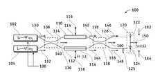
図1は、本発明の一実施形態による、光学ヘテロダインを備える広範囲チューニング可能な二重平衡フォトニック混合器100(フォトニック混合器100)を示している。フォトニック混合器100は、第1のレーザ102、第2のレーザ104、及び第1のオプティカルカプラ108を含むLO段階と、第1の電気光学位相変調器110、第2の電気光学位相変調器112、及び第2のオプティカルカプラ118を含むRF段階と、光検出器120とを備える。本明細書において、電気光学位相変調器、位相変調器、及び光学位相変調器は交換可能に使用される。 FIG. 1 shows a widely tunable double balanced photonic mixer 100 (photonic mixer 100) with optical heterodyne, according to one embodiment of the invention. The
第1のレーザ102は、制御信号106により制御される第1の周波数ω1を含む第1の光学信号130を生成する。第1のレーザ102は、限定しないが、シリコン、少なくとも一つのIII族元素(国際純正応用化学連合(IUPAC)13群)と少なくとも一つのV族元素(IUPAC15群)とを含むIII−V族化合物、又は他の適切な材料といった半導体を含む。第1のレーザ102は、例えば限定しないが、約100THz〜約500THzの第1の周波数ω1の周波数範囲内、又は他の適切な動作範囲内で動作する。第1の光学信号130は、第1のレーザ102から第1の信号経路134/128中に放出される。本明細書では、信号経路、光学信号経路、及び光導波路信号経路は交換可能に使用される。The
第2のレーザ104は、制御信号106により制御される第2の周波数ω2を含む第2の光学信号132を生成する。第2のレーザ104は、限定しないが、シリコン、III−V族化合物、又は他の適切な材料といった半導体を含む。第2のレーザ104は、例えば限定しないが、約100THz〜約500THzの第2の周波数ω2の周波数範囲内、又は他の適切な動作範囲内で動作する。第2の光学信号132は、第2のレーザ104から第2の信号経路136/138中に放出される。The
第1の信号経路134/128は、光(例えば、第1の光学信号130)を、第1のレーザ102から第1のオプティカルカプラ108中へ、次いで第1の電気光学位相変調器110及び第2のオプティカルカプラ118を通って光検出器120へと伝送する光導波路を含む。 The
第2の信号経路136/138は、光(例えば、第2の光学信号132)を、第2のレーザ104から第1のオプティカルカプラ108中へ、次いで第2の電気光学位相変調器112及び第2のオプティカルカプラ118を通って光検出器120へと伝送する光導波路を含む。 The
第1のオプティカルカプラ108は、第1の光導波路信号経路134内の第1の光学信号130と、第2の光導波路136内の第2の光学信号132とを光学的に結合し、局部発振器(LO)光学信号140を生成するように構成される。LO光学信号140は、第1の光導波路信号経路134及び第2の光導波路136の両方に伝送され、LO周波数Δωを含む。LO周波数Δωは、|ω1−ω2|、すなわち第1の光学信号130の第1の周波数ω1と第2の光学信号132の第2の周波数ω2との差である。第1のレーザ102及び第2のレーザ104と組み合わせた第1のオプティカルカプラ108は、第1の周波数ω1及び第2の周波数ω2を制御することにより制御できる局部発振器機能を提供する。第1の周波数ω1及び第2の周波数ω2を制御することにより、LO周波数Δωは、例えば限定しないが、約0Hz〜1Hzの広くチューニング可能な周波数範囲内、又は他の適切な周波数範囲内で動作させることができる。The first
第1の電気光学位相変調器110は、無線周波数電気信号116を用いて第1の光導波路信号経路134内のLO光学信号140を電気光学的に変調し、第1の位相変調光学信号142を生成するように構成される。本発明の実施形態による光混合器の場合、無線周波数電気信号116は、例えば限定しないが、0Hz(DC)のベースバンド変調、又は他の適切なベースバンド変調を含む。0Hz信号を含む無線周波数電気信号116の場合、第1の位相変調光学信号142はLO光学信号140を含み、この信号の周波数に変化はないが、例えば限定しないが、増幅されているか、位相シフトしているか、又は周波数の変化以外の他の変化を有している。いくつかの実施形態では、第1の電気光学位相変調器110は省略可能であり、LO光学信号140は変化せずに第2のオプティカルカプラ118に渡される。 The first electro-
第1の電気光学位相変調器110は、限定しないが、シリコン、III−V族化合物、又は他の適切な材料といった半導体を含む。変調器は、低Vpi位相変調器(電界吸収型(EA)でない)を含む。電界吸収型変調器(EAM)は、電圧を介してレーザビームの強度を変調するために使用できる半導体装置である。その動作原理は、フランツ−ケルディッシュ効果、すなわち印加される電界によって生じ、バンドギャップエネルギー(すなわち吸収エッジのフォトンエネルギー)を変化させるが、通常は電界による担体の励起を伴わない吸収スペクトルの変化に基づいている。変調器技術の向上により、効率を上昇させることができる(駆動電圧又はVpiの低下)。 The first electro-
マッハ−ツェンダー(MZ)変調器の半波電圧、VΠ(又はVpi)は、通常、MZ変調器の各枝路内の信号が同相である印加電圧と、それら信号のΠラジアン位相がずれている印加電圧との差に規定される。換言すれば、VΠは最大出力信号電力と最小出力信号電力との電圧差である。πの位相変化を引き起こすために必要な電圧を半波電圧(VΠ)と呼ぶ。ポッケルスセルの場合、半波電圧(VΠ)は数百ボルト、場合によっては数千ボルトでありうるので、高圧増幅器が必要になる。適切な電子回路は、このような大きな電圧を数ナノ秒内で変換することができ、高速光スイッチとしてEOMを使用することを可能にする。一体型導波路変調器の場合、半波電圧(VΠ)は、限定しないが、10ボルト未満である。 The half-wave voltage of the Mach-Zehnder (MZ) modulator, V 又 は (or Vpi), is usually out of phase with the applied voltage at which the signals in each branch of the MZ modulator are in phase with the Π radians of those signals. It is defined as the difference from the applied voltage. In other words, VΠ is a voltage difference between the maximum output signal power and the minimum output signal power. The voltage required to cause the phase change of π is called a half wave voltage (VΠ). In the case of a Pockels cell, the half-wave voltage (VΠ) can be hundreds of volts, and in some cases thousands of volts, requiring a high voltage amplifier. Appropriate electronic circuitry can convert such large voltages within a few nanoseconds, making it possible to use the EOM as a high-speed optical switch. In the case of an integrated waveguide modulator, the half-wave voltage (VΠ) is less than 10 volts, although not limited.
第2の電気光学位相変調器112は、無線周波数電気信号116を用いて第2の光導波路信号経路136内の局部発振器光学信号140を電気光学的に変調し、第2の位相変調光学信号144を生成するように構成される。無線周波数信号116が周波数ΩのRF信号を含む場合、第2の位相変調光学信号144は、周波数Ωによって変調された局部発振器光学信号140を含む。 The second electro-
第2のオプティカルカプラ118は、第1の位相変調光学信号142及び第2の位相変調光学信号144を光学的に結合し、局部発振器信号140(RF段階入力光学信号140)の局部発振器周波数が混合した無線周波数電気信号116のRF周波数を含む強度変調信号160を生成するように構成される。第1の信号経路134は、強度変調信号160を第1の強度光学信号146として導くように構成され、第2の信号経路136は強度変調信号160を第2の強度光学信号148として導くように構成される。いくつかの実施形態では、光検出器120が相補型金属酸化膜半導体(CMOS)回路を含む場合、半サイクル位相遅延125が第2の光導波路信号経路138に加えられ、相信号を反転させて補型回路を駆動する。第1の強度光学信号146及び第2の強度光学信号148は、周波数Ωによって変調されたLO光学信号140を含む。 The second
光検出器120は、第1の電気信号162として第1の強度光学信号146を光検出し、第2の電気信号164として第2の強度光学信号148を光検出するように構成される。光検出器120は、例えば限定しないが、シリコンゲルマニウム(SiGe)、III−V族化合物、又は他の適切な材料といった半導体を含む。光検出器120は、例えば限定しないが、単一の光検出器、二重平衡光検出器、又は他の適切な光検出器を含む。 The
光検出器120は、第1の光検出器回路122及び第2の光検出器回路124を含む。第1の光検出器回路122は、第1の光導波路信号経路128から第1の強度光学信号146を受信して、第1の強度光学信号146を第1の電気信号162に変換する。第2の光検出器回路124は、第2の光導波路信号経路138から第2の強度光学信号148を受信して、第2の強度光学信号148を第2の電気信号164に変換する。第1の電気信号162と第2の電気信号164とが合成されて出力信号150が生成される。電気信号150(出力信号150)は、周波数Ωにより変調されたLO光学信号140、すなわちΔω±Ωを含む。The
フォトニックRF混合器機能は、入力RF信号116と、第1のレーザ102の第1の光周波数ω1及び第2のレーザ104の第2の光周波数ω2の光ヘテロダインとの間の電気光学的相互作用により達成される。システム100では、ω1とω2との間の差周波数Δωが同等の局部発振器信号140として働く。システム100に電気的な局部発振器は適用されない。電気光学位相変調器110/112に対する一定の位相バイアスの調節により、周波数混合出力が最大化され、RF及び局部発振器周波数成分出力が最小化される。出力される中間周波数(IF)と、RF及びLO間の高分離が達成される。The photonic RF mixer function is an electro-optic between the
当業者であれば、本明細書に開示される実施形態に関連して記載される種々の例示的なブロック、モジュール、回路、及び処理論理が、ハードウェア、コンピュータで読込可能なソフトウェア、ファームウェア、又はこれらの他の組み合わせにおいて実施されうることを理解するであろう。ハードウェア、ファームウェア、及びソフトウェアのこのような互換性及び適合性を明確に説明するために、種々の例示的な構成要素、ブロック、モジュール、回路、及びステップを、概してそれらの機能性という観点から記載する。 Those skilled in the art will recognize that the various exemplary blocks, modules, circuits, and processing logic described in connection with the embodiments disclosed herein are hardware, computer readable software, firmware, Or it will be understood that it may be implemented in other combinations of these. To clearly illustrate such compatibility and compatibility of hardware, firmware, and software, various illustrative components, blocks, modules, circuits, and steps are generally viewed in terms of their functionality. Describe.
いくつかの実施形態では、システム100は、本明細書に記載されるそれぞれの動作に適した任意の数のレーザ、任意の数の光検出器、任意の数のオプティカルカプラ、任意の数の導波路、任意の数の光変調器、及び/又は任意の数の他のモジュールを含む。例示されるシステム100は、説明を容易にするために単純な実施形態を示している。システム100の上述の要素及びその他の要素は、相互接続されて、システム100の種々の要素間の通信を可能にする。 In some embodiments, the
このような機能性が、ハードウェアとして実施されるか、ファームウェアとして実施されるか、又はソフトウェアとして実施されるかは、全体のシステムに課される使用上及び設計上の特定の制約によって決まる。本明細書に記載の概念をよく知る者であれば、特定のアプリケーションの各々に適切な方式で、このような機能性を実施することができるが、そのような実装態様の意思決定は、本実施形態の範囲からの逸脱と解釈されるべきでない。 Whether such functionality is implemented as hardware, firmware or software depends upon the specific constraints in use and design imposed on the overall system. Anyone familiar with the concepts described herein can implement such functionality in a manner appropriate for each particular application, but such implementation decisions are It should not be construed as a departure from the scope of the embodiments.
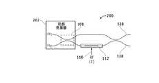
図2は、本発明の一実施形態による二波長平衡デバイス200(光学/RF混合)を示している。fLO±n*fsignal(n=1,2...は整数)の項のみが光学混合器202(局部発振器202)によって発生し、fLOのそれよりも高次の高調波(高次スパーなし)は発生せず、よってさらにクリーンな出力が生成される(ここで、fsignalはΩであり、fLOはΔωである)。二波長平衡デバイス200は、例えば限定しないが、約0.1GHz〜約110GHzのfsignal又はfLOの周波数範囲で動作する。FIG. 2 illustrates a dual wavelength balancing device 200 (optical / RF mixing) according to one embodiment of the present invention. Only the term fLO ± n * fsignal (where n = 1, 2... is an integer) is generated by the optical mixer 202 (local oscillator 202) and higher harmonics (higher order) than that of fLO No spur) occurs, thus producing a cleaner output (where fsignal is Ω and fLO is Δω). The dual wavelength
図3は、本発明の一実施形態による、フォトニックRF発振器/混合器と一体化された二重平衡ブリッジEO変調器(システム300)を示している。システム300は、RF変調(RF)段階(110/112)から分離された変調(LO)段階306/308において局部発振器(LO)信号304(図1のΔω)に対して光学的混合を実行するオプティカルカプラ108を含むフォトニックRF発振器を備える。システム300の要素について、図1及び図7の説明と併せて説明する。図1に示し、図1に関連して説明するように、RF段階は、第1の電気光学位相変調器(例えば、電気光学位相変調器110)、第2の電気光学位相変調器(例えば、第2の電気光学位相変調器112)、第2のオプティカルカプラ118、及び図1において説明したRF段階の他の要素を含む。LO段階は、第3の電気光学位相変調器306、第4の電気光学位相変調器308、第1のオプティカルカプラ108、及び他の要素を含む。いくつかの構成では、複数の段階を使用してもよい。 FIG. 3 illustrates a double balanced bridge EO modulator (system 300) integrated with a photonic RF oscillator / mixer, according to one embodiment of the invention. The
この構成では、第1の信号経路128は、レーザ302から光学信号310(レーザ光学信号310)のような光を第1の電気光学位相変調器110中に、次いで第2のオプティカルカプラ118、第3の電気光学位相変調器306及び第1のオプティカルカプラ108を通して光検出器120(図3の光検出器122及び124)へと伝達する光導波路を含む。第2の光学経路138は、レーザ302から光学信号310のような光を第2の電気光学位相変調器112中に、次いで第2のオプティカルカプラ118、第4の電気光学位相変調器308及び第1のオプティカルカプラ108を通して光検出器120(図3の光検出器122及び124)へと伝達する光導波路を含む。 In this configuration, the
このような構成では、レーザ302は、無線周波数電気信号116を用いて第1の電気光学位相変調器110及び第2の電気光学位相変調器112により位相変調された光学信号310を発生させるように構成される。図3に示すように、第2のオプティカルカプラ118は、第1の電気光学位相変調器110からの第1の位相変調光学信号142(図1)と、第2の電気光学位相変調器112からの第2の位相変調光学信号144(図1)とを光学的に結合し、強度変調信号160を生成するように構成される。このような構成では、強度変調信号160は、局部発振器(LO)信号304を用いて第3の電気光学位相変調器306及び第4の電気光学位相変調器308(例えば、第3の電気光学位相変調器306及び第4の電気光学位相変調器308は、共に局部発振器(LO)信号304により駆動される)により位相変調される。これにより、強度変調信号160は、局部発振器光学信号140の局部発振器周波数が混合した無線周波数電気信号116のRF周波数を含む。線形システムでは、RF変調(RF段階)及びLO変調(LO段階)は、どのような順序で行われてもよく、いずれの順序でも結果はほぼ同じである。 In such a configuration, the
自己発生RF源であるシステム300は、例えば限定しないが、固定の又はチューニング可能な発振周波数を含む電気光学発振器(OEO)を備える。このようにして、システム300(フォトニックRF混合器300)の出力におけるRF及びLO周波数は、バイアス位相調節により最小化される。LO発生は、RFシンセサイザを用いることなく、例えば限定しないがMHzからTHzの範囲内でチューニングし、Kバンドを含む高周波数からWバンド周波数に変換することができる。 The
例えば限定しないが、LO変調器出力及びRF変調器出力の両方に平衡ブリッジ出力を形成するオプティカルカプラ108/118のような、単一モード又は多重モード干渉オプティカルカプラを使用するために、LO信号304及び入力RF信号116(RF信号116)がさらに構造化されることにより、変調器バイアス調節によって、出力される中間周波数(IF)信号150のLO及びRF周波数成分が低減し、平衡検波器を用いる出力中間周波数(IF)信号150における同相雑音が低減し、平衡検波器を用いる出力中間周波数(IF)信号150における変換利得が増大する。 To use a single mode or multimode interference optical coupler, such as, but not limited to, an
二重平衡ブリッジ電気光学位相変調器110/112(電気光学位相変調器110/112)、二つの平衡光検出器回路122/124からなる組を含む光検出器120、及びレーザ302(図1の102/104)は、別個の構成要素に構成されても、単一の半導体基板に一体化されてもよい。 A dual balanced bridge electro-
図4は、本発明の一実施形態による、方向性カプラに基づくMZ変調器及び光検出器(システム400)と一体化されたデュアル細線レーザ設計を示している。システム400は、デュアル細線レーザエリア402、チューニング信号404、制御ループ406、及び図1の説明において説明した要素を含む。DCバイアス114又は熱バイアス法は、電気信号150のような出力される中間周波数(IF)信号におけるLO信号(Δω)及びRF信号(Ω)を最小化する。第1のレーザ102及び第2のレーザ104は、それぞれフリーランニングであるか、又は基準信号にロックされている。 FIG. 4 illustrates a dual wire laser design integrated with a directional coupler based MZ modulator and photodetector (system 400), according to one embodiment of the present invention.
第1のレーザ102及び第2のレーザ104の一方又は両方のチューニングは、電流、又は温度によって実行され、無線周波数シンセサイザを用いることなく、例えば限定しないが、MHz〜THzの範囲にわたり、KバンドからWバンドを含む高周波数をカバーするLO信号を発生させる。制御ループ406は、チューニング信号404及びLO信号(Δω)及びRF信号(Ω)に基づいて周波数ロック信号408及びDCバイアス114を制御する。チューニング信号404は、基準信号と、光学信号経路134及び136内のレーザビームの光学ヘテロダインとの比較により取得される。光学ヘテロダインは、例えば限定しないが、信号経路134、136から光学信号をタッピングして、光検出器において合成すること、又は第1のカプラの後で光学信号を直接タッピングすること(例えば、図7のタップ信号778)を含む任意の数のアプローチにより達成することができる。 Tuning of one or both of the
検出器120は、出力光から離れた位置に、単一の光検出器、又は二つの平衡光検出器(例えば、122及び124)からなる組を備え、複数の光ファイバ又は光学撮像システムを介して二つの平衡光検出器の組に出力光が送達することができる。 The
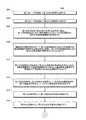
図5は、本発明の一実施形態による電気光学ヘテロダイン法のプロセス500を示す例示的フロー図である。プロセス500に関連して実行される種々のタスクは、ソフトウェア、ハードウェア、ファームウェア、プロセス方法を実行するためのコンピュータで実行可能な命令を有するコンピュータで読込可能な媒体、又はそれらの何らかの組み合わせにより実行される。プロセス500は、任意の数の追加タスク又は別タスクを含んでもよく、図5に示されるタスクは必ずしも図示の順序で実行されなくともよく、プロセス500は、本明細書に記載しない追加の機能性を有するもっと包括的な手続き又はプロセスに組み込まれてもよい。いくつかの実施形態では、プロセス500の各部分は、異なる要素、すなわち、第1のレーザ102、第2のレーザ104、第1のオプティカルカプラ108、第1の電気光学位相変調器110、第2の電気光学位相変調器112、第2のオプティカルカプラ118、光検出器120などにより実行されうる。プロセス500は、図1〜4及び7に示す実施形態に類似の機能、材料、及び構造を有している。したがって、共通のフィーチャ、機能、及び要素についてはここでは繰り返さない。 FIG. 5 is an exemplary flow diagram illustrating an electro-
プロセス500は、第1のレーザ(例えば、第1のレーザ102)を制御して第1の光学信号(例えば、第1の光学信号130)を生成することにより開始される(タスク502)。
プロセス500では、続いて、第2のレーザ(例えば、第2のレーザ104)を制御して第2の光学信号132を生成する(タスク504)。
プロセス500では、続いて、第1の光学信号130と第2の光学信号132とを光学的に結合し、第1の信号経路(例えば、第1の信号経路134/128)及び第2の信号経路(例えば、第2の信号経路136/138)からなる二つの信号経路内を伝搬する局部発振器信号(例えば、局部発振器信号140)を生成する(タスク506)。
プロセス500では、続いて、無線周波数電気信号(例えば、無線周波数電気信号116)を用いて、第1の信号経路134/128及び第2の信号経路136/138内の局部発振器光学信号140を電気光学的に位相変調し、第1の位相変調光学信号(例えば、第1の位相変調光学信号142)及び第2の位相変調光学信号(例えば、第2の位相変調光学信号144)をそれぞれ生成する(タスク508)。
プロセス500では、続いて、第1の位相変調光学信号142及び第2の位相変調光学信号144を光学的に結合し、局部発振器光学信号140の局部発振器周波数が混合した無線周波数電気信号116のRF周波数を含む強度変調信号(例えば、強度変調信号160)を生成する(タスク510)。 The
プロセス500では、続いて、第1の信号経路134/128内に第1の強度光学信号(例えば、第1の強度光学信号146)として、及び第2の信号経路136/138内に第2の強度光学信号(例えば、第2の強度光学信号148)として、強度変調信号160を生成する(タスク512)。
プロセス500では、続いて、第1の電気信号(例えば、第1の電気信号162)として第1の強度光学信号146を光検出する(タスク514)。 The
プロセス500では、続いて、第2の電気信号(例えば、第2の電気信号164)として第2の強度光学信号148を光検出する(タスク516)。
プロセス500では、続いて、第1の電気信号162と第2の電気信号164とを合成して出力信号(例えば、出力信号150)を生成する(タスク518)。 The
プロセス500では、続いて、第1の電気信号162及び第2の電気信号164の同相を除去して出力信号150を生成する(タスク520)。
プロセス500では、続いて、第1のレーザ102及び第2のレーザ104の一方又両方を、制御信号106又は周波数ロック信号408(図4)のような電流によりチューニングする(タスク522)。
プロセス500では、続いて、無線周波数シンセサイザを用いずに一定範囲の周波数にわたって局部発振器信号140を発生させる(タスク524)。
プロセス500では、続いて、レーザ(例えば、レーザ302(例として、図3及び7))を制御して光学信号(例えば、光学信号310((例として、図3及び7))を生成する(タスク526)。
プロセス500では、続いて、外部信号(例えば、外部局部発振器信号304(例として、図3及び7))を用いて光学信号310を光電子光学的に変調し、第1の光学信号130及び第2の光学信号132を生成する(タスク528)。外部局部発振器信号304は、図7に示すように発生する。
プロセス500では、続いて、第1の光学信号130及び第2の光学信号132のヘテロダインにより局部発振器光学信号140を発生させる(タスク530)。 The
プロセス500では、続いて、出力信号150の局部発振器信号140及び無線周波数電気信号160の信号漏れを最小化する(タスク532)。
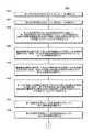
図6は、本発明の一実施形態による電気光学変調器の生産プロセスを示す例示的フロー図である。プロセス600に関連して実行される種々のタスクは、ソフトウェア、ハードウェア、ファームウェア、プロセス方法を実行するためのコンピュータで実行可能な命令を有するコンピュータで読込可能な媒体、又はそれらの何らかの組み合わせにより実行される。プロセス600は、任意の数の追加タスク又は別タスクを含んでもよく、図6に示されるタスクは必ずしも図示の順序で実行されなくともよく、プロセス600は、本明細書に記載しない追加の機能性を有するもっと包括的な手続き又はプロセスに組み込まれてもよい。いくつかの実施形態では、プロセス600の各部分は、異なる要素、すなわち、第1のレーザ102、第2のレーザ104、第1のオプティカルカプラ108、第1の電気光学位相変調器110、第2の電気光学位相変調器112、第3の電気光学位相変調器306、第4の電気光学位相変調器308、外部局部発振器信号304、第2のオプティカルカプラ118、光検出器120などにより実行されうる。プロセス600は、図1〜4、及び7に示す実施形態と同様の機能、材料、及び構造を有している。したがって、共通のフィーチャ、機能、及び要素についてはここでは繰り返さない。 FIG. 6 is an exemplary flow diagram illustrating a production process for an electro-optic modulator according to an embodiment of the present invention. The various tasks performed in connection with
プロセス600は、第1の光学信号(例えば、第1の光学信号130/712)を生成するように第1のレーザ(例えば、第1のレーザ102)を構成することにより開始される(タスク602)。
プロセス600では、続いて、第2の光学信号(例えば、第2の光学信号132/714)を生成するように第2のレーザ(例えば、第2のレーザ104)を構成する(タスク604)。
プロセス600では、続いて、第1の光学信号130及び第2の光学信号132を光学的に結合して、第1の信号経路(例えば、第1の信号経路134/128及び第2の信号経路(例えば第2の信号経路136/138)からなる二つの信号経路内を伝搬する局部発振器信号を含むRF段階入力光学信号(例えば、LO光学信号140、及び/又はRF段階入力光学信号722/724、図7)を生成するように、RF段階入力オプティカルカプラ(例えば、第1のオプティカルカプラ108)を構成する(タスク606)。
プロセス600では、続いて、無線周波数電気信号(例えば、無線周波数電気信号116)を用いて第1の信号経路128内のRF段階入力光学信号140/722を電気光学的に変調し、第1のRF段階位相変調光学信号(例えば、位相変調光学信号142、図1)を生成するように、第1の光変調器(例えば、第1の光変調器110)を構成する(タスク608)。
プロセス600では、続いて、無線周波数電気信号116を用いて第2の信号経路138内のRF段階入力光学信号140/724を電気光学的に変調し、第2のRF段階位相変調光学信号(例えば、位相変調光学信号144、図1)を生成するように、第2の光変調器(例えば、第2の光変調器112)を構成する(タスク610)。
プロセス600では、続いて、第1のRF段階位相変調光学信号142及び第2のRF段階位相変調光学信号144を光学的に結合し、第1の信号経路128/134及び第2の信号経路138/136内の無線周波数電気信号116の周波数を含む強度変調出力信号(例えば、強度変調出力信号160/770)を生成するように、RF段階オプティカルカプラ118を構成する(タスク612)。 The
プロセス600では、続いて、第1の強度光学信号(例えば、第1の強度光学信号146/746)として強度変調信号160/770を導くように、第1の信号経路128/134を構成する(タスク614)。 The
プロセス600では、続いて、第2の強度光学信号(例えば、第2の強度光学信号148/750)として強度変調信号160/770を導くように、第2の信号経路138/136を構成する(タスク616)。 The
プロセス600では、続いて、第1の電気信号(例えば、第1の電気信号162)として第1の強度光学信号146/746を光検出するように、光検出器(例えば、光検出器120/122)を構成する(タスク618)。
プロセス600では、続いて、第2の電気信号(例えば、第2の電気信号164)として第2の強度光学信号148/750を光検出するように、光検出器120/124を構成する(タスク620)。 The
プロセス600では、続いて、第1の電気信号162と第2の電気信号164とを合成して出力信号(例えば、出力信号150)を生成するように、光検出器120を構成する(タスク622)。 The
プロセス600では、続いて、第1の電気信号162及び第2の電気信号164の同相を除去して出力信号150を生成するように、光検出器120を構成する(タスク624)。 The
プロセス600では、続いて、光学信号(例えば、光学信号310)を生成するように、レーザ(例えば、レーザ302)を構成する(タスク626)。
プロセス600では、続いて、外部局部発振器信号(例えば、外部局部発振器信号304)を用いて光学信号310を電気光学的に変調し、第1の光学信号130/712及び第2の光学信号132/714を生成するように、第3及び第4の光変調器(例えば、第3及び第4の光変調器306/308)を構成する(タスク628)。
図7は、本発明の一実施形態による、一体型光電子発振器700(システム700)を有するフォトニックRF混合器を示している。システム700の要素のいくつかについて、図1及び図3の説明と併せて説明する。システム700は、第1の信号経路712/134/128を通って電気光学位相変調器306へ、及び第2の信号経路714/136/138を通って電気光学位相変調器308へそれぞれ向かう強度の等しい二つのビーム712及び714を介して供給されるRF段階入力光学信号722/724へと、光学信号310を分割する光学スプリッタ708を備えている。図1及び3に示し、図1及び3に関して説明したように、RF段階は、第1の電気光学位相変調器110、第2の電気光学位相変調器112、第2のオプティカルカプラ118、及び図1において説明したRF段階の他の要素を含む。LO段階は、第3の電気光学位相変調器306、第4の電気光学位相変調器308、第1のオプティカルカプラ108、及び他の要素を含む。いくつかの構成では、複数の段階が使用される。 FIG. 7 illustrates a photonic RF mixer having an integrated optoelectronic oscillator 700 (system 700), according to one embodiment of the invention. Some of the elements of
このような構成では、第1の信号経路712/134/128は、光(例えば、光学信号310)を、レーザ302から第3の電気光学位相変調器306中へ、次いで第1のオプティカルカプラ108、第1の電気光学位相変調器110、及び第2のオプティカルカプラ118を通って光検出器120へと伝送する光導波路を含む。第2の信号経路714/136/138は、光(例えば、光学信号310)を、レーザ302から第4の電気光学位相変調器308中へ、次いで第1のオプティカルカプラ108、第2の電気光学位相変調器112、及び第2のオプティカルカプラ118を通って光検出器120へと伝送する光導波路を含む。 In such a configuration, the
RF段階入力光学信号712/722/714/724は、二つの第1の電気光学位相変調器306/308をそれぞれ通って伝搬し、外部光電子発振器774が発生させる外部局部発振器(LO)信号304によって変調される。このようにして、電気光学位相変調器306は、外部局部発振器信号304を用いて第1の信号経路134内のレーザ光学信号310を電気光学的に位相変調し、第1の信号経路134内に第1のLO段階位相変調信号716を生成する。同様に、電気光学位相変調器308は、外部局部発振器信号304を用いて第2の信号経路136内のレーザ光学信号310を電気光学的に位相変調し、第2の信号経路136内に第2のLO段階位相変調信号718を生成する。 The RF stage input
第1のLO段階位相変調光学信号716及び第2のLO段階位相変調光学信号718(二つの変調ビーム716及び718)は、第1段階電気光学位相変調器306/308の端部に一体化された(2×2の)LO段階オプティカルカプラ108によって合成されて、二つの第1段階変調ビーム722及び724(RF段階入力光学信号722及び724)を生成する。 The first LO stage phase modulated
第1の(2×2)LOオプティカルカプラ108からのRF段階入力光学信号722及び724は、二つの第2段階電気光学位相変調器110/112の入力に結合される。RF段階入力光学信号722及び724は、第2段階電気光学位相変調器110/112(光変調器110/112)に印加される入力RF信号116によって変調される。このようにして、LO段階オプティカルカプラ108は、第1のLO段階位相変調光学信号716と第2のLO段階位相変調光学信号718を光学的に結合して、第1の信号経路134及び第2の信号経路136内に外部局部発振器信号304を含むRF段階入力光学信号722/724を生成する。外部局部発振器信号304は、RF段階の外側にあるが、例えば限定しないが、一体型のシステム、回路、又は基板(図7に例示的に示す)内に発生させることができる。 The RF stage input optical signals 722 and 724 from the first (2 × 2) LO
第1の光変調器110は、無線周波数電気信号116を用いて第1の信号経路128内のRF段階入力光学信号722を電気光学的に変調し、第1のRF段階位相変調光学信号732を生成する。第2の光変調器112は、無線周波数電気信号116を用いて第2の信号経路138内のRF段階入力光学信号724を電気光学的に変調し、第2のRF段階位相変調光学信号734を生成する。 The first
第2段階変調ビーム732及び734(RF段階位相変調光学信号732及び734)は、二つの(1×2)オプティカルカプラ118(RF段階オプティカルカプラ118)により四つのポートに分割される。(1×2)オプティカルカプラ118の一つのポート、又は各(1×2)RF段階オプティカルカプラ118の一つのポートは、一又は複数のQ係数の高い光共振器フィルタ736(光学フィルタ736)に外部局部発振器信号304のフィードバック入力として送られ、各(1×2)RF段階オプティカルカプラ118の他の二つのポートは、RF段階オプティカルカプラ118によって合成されて第1の信号経路128及び第2の信号経路138から出力される。 Second stage modulated
RF段階オプティカルカプラ118は、第1のRF段階位相変調光学信号732及び第2のRF段階位相変調光学信号734を光学的に結合し、第1の信号経路128及び第2の信号経路138内の無線周波数電気信号116の周波数を含む強度変調光学信号770を生成する。これにより、強度変調出力信号770は、外部局部発振器信号304の局部発振器周波数と混合された無線周波数電気信号116のRF周波数を含む。 The RF stage
第1の信号経路128は、強度変調信号770を第1の強度光学信号746として導き、第2の信号経路138は強度変調信号770を第2の強度光学信号750として導く。 The
光検出器122は、第1の電気信号162として第1の強度光学信号746を光検出し、第2の電気信号164として第2の強度光学信号750を光検出する。光検出器120は、第1の電気信号162及び第2の電気信号164を合成して出力信号772を生成する。光検出器122は、第1の電気信号162と第2の電気信号164の同相を除去して出力信号772を生成する。 The
外部局部発振器信号304は、第1のRF段階位相変調光学信号732又は第2のRf段階位相変調光学信号734をノード776においてテーピングオフ(taping off)することにより発生し、タップ(tapped)信号778を生成してこのタップ信号778をフィードバック光電子発振器ループ780に送る。 The external
RFバイアス制御782は、光変調器306/308/110/112を調節することにより無線周波数電気信号116及び局部発振器信号304の漏れを最小化して出力信号772を最適化するために使用される。 The
光電子発振器774は、外部周波数シンセサイザを用いることなく、所望の局部発振器周波数を発生させるようにチューニングされる。 The
システム700は、光電子発振器340と二重平衡フォトニック混合器との一体化を可能にする。フィードバック光学信号784は、高Q係数RFフィルタ786によりフィルタリングされ、光検出器760により受け取られる。光検出器760の出力762は、RF増幅器764によって増幅されてフィードバック光電子発振器を形成する。
したがって、フォトニックRF混合器は二つの機能を一つのパッケージに統合する。周波数混合に必要なLO信号は、外部のLO源からではなく、システム700自体により発生する。LO周波数は、フィードバックループ内において光学及びRFフィルタにより選択される。超低位相雑音RF信号の発生が光電子発振器774において実現する。フィードバック光電子発振器ループ780内の光学フィルタ736は、例えば限定しないが、高Q係数マイクロリング共振器、ささやきの回廊(wisper−gallary)モードの共振器、一体型光導波路遅延線、外部繊維コイル遅延線、又は他の狭帯域幅高Q係数光周波数選択的デバイスとすることができる。 Thus, the photonic RF mixer integrates two functions into one package. The LO signal required for frequency mixing is generated by the
図8は、本発明の一実施形態による電気光学変調器の生産プロセス800を示す例示的フロー図である。
プロセス800に関連して実行される種々のタスクは、ソフトウェア、ハードウェア、ファームウェア、プロセス方法を実行するためのコンピュータで実行可能な命令を有するコンピュータで読込可能な媒体、又はそれらの何らかの組み合わせにより実行される。プロセス800は、任意の数の追加タスク又は別タスクを含んでもよく、図8に示されるタスクは必ずしも図示の順序で実行されなくともよく、プロセス800は、本明細書に詳細に記載しない追加の機能性を有するもっと包括的な手続き又はプロセスに組み込まれてもよい。いくつかの実施形態では、プロセス600の各部分は、異なる要素、すなわち、レーザ302、外部局部発振器信号304、電気光学位相変調器306、電気光学位相変調器308、電気光学位相変調器110、電気光学位相変調器112などにより実行されうる。プロセス800は、図1〜4及び7に示す実施形態と同様の機能、材料、及び構造を有しうる。したがって、共通のフィーチャ、機能、及び要素についてはここでは繰り返さない。FIG. 8 is an exemplary flow diagram illustrating an electro-optic
The various tasks performed in connection with
プロセス800は、レーザ光学信号(例えば、レーザ光学信号310)を生成するようにレーザ(例えば、レーザ302(例として、図3及び7))を構成することにより開始される(タスク802)。
プロセス800では、続いて、第1の信号経路(例えば、第1の信号経路134)を介して第3の光学位相変調器(例えば、光学位相変調器306)へ、及び第2の信号経路(例えば第2の信号経路136)を介して第4の光学位相変調器(例えば、光学位相変調器308)へ、それぞれ供給されるRF段階入力光学信号(例えば、RF段階入力光学信号140/712/714/722/724(例として、及び、図3に適用した場合))に、レーザ光学信号310を分割するように光学スプリッタ(例えば、光学スプリッタ708(例として、図7、及び図3に図7を適用した場合))を構成する(タスク804)。
プロセス800では、続いて、外部局部発振器信号(例えば、外部局部発振器信号304)を用いて第1の信号経路134内のレーザ光学信号310を電気光学的に位相変調し、第1の信号経路134内に第1のLO段階位相変調信号(例えば、第1のLO段階位相変調信号716)を生成するように、第3の光変調器306(例として、図7)を構成する(タスク806)。
プロセス800では、続いて、外部局部発振器信号304を用いて第2の信号経路136内のレーザ光学信号310を電気光学的に位相変調し、第2の信号経路136内に第2のLO段階位相変調信号718を生成するように、第4の光変調器308(例として、図7)を構成する(タスク808)。
プロセス800では、続いて、第1のLO段階位相変調光学信号716と第2のLO段階位相変調光学信号718を光学的に結合して、第1の信号経路134及び第2の信号経路136内に、それぞれ局部発振器信号304を含むRF段階入力光学信号(例えば、RF段階入力光学信号722/724)を生成するように、LO段階オプティカルカプラ(例えば、LO段階オプティカルカプラ108(例として、図7))を構成する(タスク810)。 The
プロセス800では、続いて、無線周波数電気信号(例えば、無線周波数電気信号116)を用いて第1の信号経路128/134内のRF段階入力光学信号722を電気光学的に変調し、第1のRF段階位相変調光学信号(例えば、第1のRF段階位相変調光学信号732)を生成するように、第1の光変調器(例えば、光変調器110(図1、3、及び7)を構成する(タスク812)。
プロセス800では、続いて、無線周波数電気信号116を用いて第2の信号経路136/138内のRF段階入力光学信号724を電気光学的に変調し、第2のRF段階位相変調光学信号(例えば、第2のRF段階位相変調光学信号734)を生成するように、第2の光変調器(例えば、光変調器112(図1、3、及び7)を構成する(タスク814)。
プロセス800では、続いて、第1のRF段階位相変調光学信号732及び第2のRF段階位相変調光学信号734を光学的に結合し、第1の信号経路128及び第2の信号経路138内に無線周波数電気信号116の周波数を含む強度変調出力信号(例えば、強度変調出力信号160/770)を生成するように、RF段階オプティカルカプラ(例えば、RF段階オプティカルカプラ118(図1、3、及び7)を構成する(タスク816)。
プロセス800では、続いて、外部局部発振器信号304を用いて第1の信号経路128/134内の強度変調出力信号160/770を電気光学的に位相変調し、第1の信号経路128/134内に第1のLO段階位相変調信号を生成するように(例えば、図7に示す第1のLO段階位相変調信号716と同様に)、(第5の)光変調器(例えば、光変調器306(例として、図3))を構成する(タスク818)。
プロセス800では、続いて、外部局部発振器信号304を用いて第2の信号経路138/136内の強度変調出力信号160/770を電気光学的に位相変調し、第2の信号経路138/136内に第2のLO段階位相変調信号を生成するように(例えば、図7に示す第2のLO段階位相変調信号718と同様に)、(第6の)光変調器(例えば、光変調器308(例として、図3))を構成する(タスク820)。 The
プロセス800では、続いて、第1のLO段階位相変調光学信号(例えば、図7に示す第1のLO段階位相変調信号716と同様)と、第2のLO段階位相変調光学信号(例えば、図7に示す第2のLO段階位相変調信号718と同様)とを光結合し、局部発振器信号160の局部発振器周波数が混合した無線周波数電気信号周波数(例えば、無線周波数信号116)の無線周波数を含む第1の信号経路128/136及び第2の信号経路138/136内の強度変調出力信号160/770を生成するように、LO段階オプティカルカプラ(例えば、第1のオプティカルカプラ108(図3))を構成する(タスク822)。
プロセス800では、続いて、第1の強度光学信号(例えば、第1の強度光学信号746)として強度変調信号770を導くように、第1の信号経路128を構成する(タスク824)。
プロセス800では、続いて、第2の強度光学信号(例えば、第2の強度光学信号750)として強度変調信号770を導くように、第2の信号経路138を構成する(タスク826)。
プロセス800では、続いて、第1の電気信号(例えば、第1の電気信号162)として第1の強度光学信号746を光検出するように、光検出器122(例えば、光検出器122)を構成する(タスク828)。
プロセス800では、続いて、第2の電気信号(例えば、第2の電気信号164)として第2の強度光学信号750を光検出するように、光検出器122を構成する(タスク830)。 The
プロセス800では、続いて、第1の電気信号162と第2の電気信号164とを合成して出力信号(例えば、出力信号772)を生成するように、光検出器122を構成する(タスク832)。 The
プロセス800では、続いて、第1の電気信号162及び第2の電気信号164の同相を除去して出力信号772を生成するように、光検出器122を構成する(タスク834)。 The
プロセス800では、続いて、第1のRF段階位相変調光学信号732又は第2のRF段階位相変調光学信号734をノード(例えば、ノード776)においてテーピングオフ(taping off)することにより局部発振器信号304を発生させ、タップ(tapped)信号(例えば、タップ信号778)を生成してこのタップ信号778をフィードバック光電子発振器ループ(例えば、フィードバック光電子発振器ループ780)に送る(タスク836)。
プロセス800では、続いて、光学位相変調器306/308/110/112のバイアスを調節することにより無線周波数電気信号116及び局部発振器信号304の漏れを最小化して出力信号772を最適化するように、RFバイアス制御782を構成する(タスク838)。
プロセス800では、続いて、外部周波数シンセサイザを用いずに所望の局部発振器周波数を発生させるよう、光電子発振器774をチューニングする(タスク840)。
このようにして、本明細書の実施形態により、電気光学周波数変換及び混合のためのシステムと方法とが提供される。 Thus, the embodiments herein provide systems and methods for electro-optic frequency conversion and mixing.
上記に少なくとも一つの例示的実施形態を提示したが、無数の変形例が存在することを理解されたい。また、本明細書に記載される一又は複数の例示的実施形態は、いかなる意味でも主題の範囲、適用性、又は構成を限定するものではない。そうではなく、上述の詳細な記載は、当業者に対し、記載された一又は複数の実施形態を実施するための便利な道路地図を提供するものである。請求の範囲に定義される範囲から逸脱することなく、要素の機能及び構成には種々の変更が可能であり、それには既知の等価物及び本特許出願の時点で予見可能な等価物が含まれることを理解されたい。 While at least one exemplary embodiment has been presented above, it should be appreciated that numerous variations exist. Also, one or more exemplary embodiments described herein are not intended to limit the scope, applicability, or configuration of the subject matter in any way. Rather, the above detailed description provides those skilled in the art with a convenient road map for implementing one or more of the described embodiments. Various changes may be made in the function and construction of the elements without departing from the scope as defined in the claims, including known equivalents and equivalents foreseeable at the time of filing this patent application. Please understand that.
本明細書において使用される「モジュール」という用語は、本明細書に記載される関連機能を実行するための、ソフトウェア、ファームウェア、ハードウェア、及びこれらの要素のいずれかの組み合わせを指す。加えて、説明のために、種々のモジュールを、個別のモジュールとして記載したが、当業者であれば分かるように、二つ以上のモジュールを組み合わせて、本発明の実施形態による関連機能を実行する単一のモジュールを形成してもよい。 The term “module” as used herein refers to software, firmware, hardware, and any combination of these elements for performing the relevant functions described herein. In addition, for purposes of explanation, the various modules have been described as separate modules, but those skilled in the art will appreciate that two or more modules may be combined to perform related functions according to embodiments of the present invention. A single module may be formed.
上述では、「接続」又は「結合」されている要素、ノード、又はフィーチャに言及している。本明細書で使用される場合、別途明確な記載がない限り、「接続された」とは、必ずしも機械的にというわけではなく、一つの要素/ノード/フィーチャが別の要素/ノード/フィーチャに直接接合されている(又は直接連絡している)ことを意味する。同様に、別途明確な記載がない限り、「結合された」とは、必ずしも機械的にというわけではなく、一つの要素/ノード/フィーチャが別の要素/ノード/フィーチャに直接又は間接的に接合されている(或いは、直接又は間接的に連絡している)ことを意味する。このように、図1〜4及び7では要素の例示的な構成を示したが、本発明の一実施形態において、追加的な仲介要素、デバイス、フィーチャ、又は構成要素が存在してもよい。 The foregoing refers to elements, nodes, or features that are “connected” or “coupled”. As used herein, unless specifically stated otherwise, “connected” is not necessarily mechanical, but one element / node / feature to another element / node / feature. It means being directly joined (or in direct contact). Similarly, unless specifically stated otherwise, “coupled” is not necessarily mechanical, but one element / node / feature joins directly or indirectly to another element / node / feature. (Or contacted directly or indirectly). Thus, while FIGS. 1-4 and 7 illustrate exemplary configurations of elements, additional mediator elements, devices, features, or components may be present in one embodiment of the invention.
本明細書で使用される用語及び表現、並びにそれらの変化形は、別途明確な記載がない限り、限定的なものではなく、変更可能なものである。その例として、「含む」という表現は、「限定せずに含む」などを意味するものと理解することができ、「例」は、説明されるアイテムの事例を提供するために使用されているのであり、その排他的又は限定的なリストではない。「従来の」、「常套的な」、「通常の」、「標準の」、「既知の」、及び同様の意味を有する表現は、記載されているアイテムを、所定の時期に限定しているわけでも、ある時期に入手可能であるアイテムに限定しているわけでもなく、現在又は未来のいずれかの時期における従来技術、常套的技術、通常の技術、又は標準的技術と理解すべきである。 The terms and expressions used in this specification, and variations thereof, are not intended to be limiting and can be changed unless explicitly stated otherwise. By way of example, the phrase “including” can be understood to mean “including but not limited to” and “examples” are used to provide examples of the items described It is not an exclusive or limited list. “Traditional”, “conventional”, “normal”, “standard”, “known”, and similar meanings limit the items described to a given time Neither is it limited to items that are available at a certain time, but should be understood as prior art, conventional technology, ordinary technology, or standard technology, either at present or in the future. .
同様に、接続詞「及び」によりリンクされた一組のアイテムは、それらアイテムの各々すべてがグループ内に存在することが必ずしも必要という意味ではなく、別途明確な記載がない限り、「及び/又は」と同義である。同様に、接続詞「又は」によりリンクされた一組のアイテムは、グループの中で必ずしも互いに排他的であるわけではなく、別途明確な記載がない限り、やはり「及び/又は」と同義である。 Similarly, a set of items linked by the conjunction “and” does not necessarily mean that each of those items must be present in the group, and “and / or” unless stated otherwise. It is synonymous with. Similarly, a set of items linked by the conjunction “or” is not necessarily mutually exclusive within a group, and is still synonymous with “and / or” unless explicitly stated otherwise.
さらに、本発明のアイテム、要素、又は構成要素が単一形で記載又は特許請求されているかもしれないが、単一形に限定されることが明確に記載されていない限り、本発明の範囲内で複数形も考慮される。一部の事例における「一又は複数の」、「少なくとも」、「限定されないが」などの広義的な用語及び表現の存在は、そのような広義的な表現がない場合に範囲を狭めることを意図している又は範囲を狭めることが必要であると解釈されるべきでない。数字により表現される値又は範囲に言及して「約」という場合、測定時に起こりうる実験誤差により生じる値を包含することを意図している。 Further, although items, elements or components of the invention may be described or claimed in a single form, the scope of the invention is not expressly stated unless limited to the single form. Plural forms are also considered. The existence of broad terms and expressions, such as “one or more”, “at least”, “but not limited” in some cases, is intended to narrow the scope in the absence of such broad expressions Should not be construed as necessary or narrowing the scope. Reference to a value or range expressed in numbers as "about" is intended to encompass values resulting from experimental error that can occur during measurement.
本明細書で使用される場合、別途明確な記載がない限り、「動作可能」とは、使用又はサービスに使用可能、適合、又は準備可能であり、特定用途に使用可能であり、且つ本明細に記載の機能又は所望の機能を実行できることを意味する。システム及びデバイスに関して、「動作可能」という表現は、システム及び/又はデバイスが完全に機能的且つ較正済みであって、起動されると記載の機能を実行するための、適用可能な実施可能要件のための要素を含み、そのような実施可能要件を満たすことを意味する。システム及び回路に関して、「動作可能」という表現は、システム及び/又は回路が完全に機能的且つ較正済みであって、起動されると記載の機能を実行するための、適用可能な実施可能要件のロジックを含み、そのような実施可能要件を満たすことを意味する。 As used herein, unless otherwise explicitly stated, “operable” means usable, adaptable or ready for use or service, usable for a particular application, and It means that the function described in the above or a desired function can be executed. With respect to systems and devices, the expression “operable” refers to an applicable enablement requirement for the system and / or device to be fully functional and calibrated and perform the described functions when activated. Means to meet such enablement requirements. With respect to systems and circuits, the expression “operable” refers to applicable enablement requirements for performing the described functions when the systems and / or circuits are fully functional and calibrated and activated. Including logic and means meeting such enablement requirements.
100 フォトニック混合器
102 第1のレーザ
104 第2のレーザ
106 制御信号
108 第1のオプティカルカプラ
110 第1の電機光学位相変調器
112 第2の電機光学位相変調器
114 DCバイアス
116 無線周波数電気信号
118 第2のオプティカルカプラ
120 光検出器
122 第1の光検出器回路
124 第2の光検出器回路
128、134 第1の信号経路
130 第1の光学信号
132 第2の光学信号
136、138 第2の信号経路
140 局部発振器(LO)光学信号
142 第1の位相変調光学信号
144 第2の位相変調光学信号
146 第1の強度光学信号
148 第2の強度光学信号
150 出力信号
160 強度変調信号
162 第1の電気信号
164 第2の電気信号
200 二波長平衡デバイス
202 光学混合器(局部発振器)
300 二重平衡ブリッジEO変調器(システム)
302 レーザ
304 局部発振器(LO)信号
306 第3の電気光学位相変調器
308 第4の電気光学位相変調器
310 光学信号
400 MZ変更器及び光検出器(システム)
402 デュアル細線レーザエリア
404 チューニング信号
406 制御ループ
408 周波数ロック信号
700 一体型電子発振器(システム)
708 光学スプリッタ
712 第1の信号経路
714 第2の信号経路
716 第1のLO段階位相変調光学信号
718 第2のLO段階位相変調光学信号
722、724 RF段階入力光学信号
732 第1のRF段階位相変調光学信号
734 第2のRF段階位相変調光学信号
736 光学フィルタ
746 第1の強度光学信号
750 第2の強度光学信号
760 光検出器
762 光検出器の出力
764 RF増幅器
770 強度変調信号
772 出力信号
774 光電子発振器
776 ノード
778 タップ信号
780 フィードバック光電子発振器ループ
782 RFバイアス制御
784 フィードバック光学信号
786 高Q係数RFフィルタDESCRIPTION OF
300 Double balanced bridge EO modulator (system)
302
402 Dual thin
708
Claims (10)
Translated fromJapanese無線周波数電気信号を用いて前記第1の信号経路及び前記第2の信号経路内の前記局部発振器信号を電気光学的に位相変調し、第1の位相変調光学信号及び第2の位相変調光学信号をそれぞれ生成することであって、前記第1の位相変調光学信号は、前記第1の信号経路内の前記局部発振器信号を増幅すること、または位相シフトすることで得られる信号であり、前記第2の位相変調光学信号は、前記第2の信号経路内の前記局部発振器信号の周波数を変化させることで得られる信号である、第1の位相変調光学信号及び第2の位相変調光学信号をそれぞれ生成すること、
前記第1の位相変調光学信号及び前記第2の位相変調光学信号を光学的に結合し、前記局部発振器信号の局部発振器周波数が混合した前記無線周波数電気信号周波数のRF周波数を含む強度変調信号を生成すること、
前記第1の信号経路内に第1の強度光学信号として、及び前記第2の信号経路内に第2の強度光学信号として、前記強度変調信号をそれぞれ生成すること、
第1の電気信号として前記第1の強度光学信号を光検出すること、
第2の電気信号として前記第2の強度光学信号を光検出すること、
前記第1の電気信号と前記第2の電気信号とを合成すること、並びに
前記第1の電気信号と前記第2の電気信号との同相を除去して出力信号を生成すること、を含む電気光学ヘテロダイン法。Optically combining the first optical signal and the second optical signal to generate a local oscillator signal that propagates in two signal paths comprised of the first signal path and the second signal path;
The local oscillator signal in the first signal path and the second signal path is electro-optically phase-modulated using a radio frequency electrical signal, and a first phase-modulated optical signal and a second phase-modulated optical signalWherein the first phase modulated optical signal is a signal obtained by amplifying or phase shifting the local oscillator signal in the first signal path, The second phase modulation optical signal is a signal obtained by changing the frequency of the local oscillator signal in the second signal path. The first phase modulation optical signal and the second phase modulation optical signal are respectively obtained by changing the frequency of the local oscillator signal in the second signal path. Generating ,
An intensity modulation signal including an RF frequency of the radio frequency electrical signal frequency obtained by optically combining the first phase modulation optical signal and the second phase modulation optical signal and mixing a local oscillator frequency of the local oscillator signal Generating,
Generating the intensity modulated signal as a first intensity optical signal in the first signal path and as a second intensity optical signal in the second signal path, respectively.
Photodetecting the first intensity optical signal as a first electrical signal;
Optically detecting the second intensity optical signal as a second electrical signal;
Combining the first electric signal and the second electric signal; and removing an in-phase between the first electric signal and the second electric signal to generate an output signal. Optical heterodyne method.
第2のレーザを制御して前記第2の光学信号を生成すること、をさらに含む請求項1に記載の前記方法。The method of claim 1, further comprising: controlling a first laser to generate the first optical signal; and controlling a second laser to generate the second optical signal. .
無線周波数シンセサイザを用いずに、一定範囲の周波数にわたって前記局部発振器信号を生成すること、をさらに含む請求項2に記載の前記方法。Further comprising tuning one or both of the first laser and the second laser with a current and generating the local oscillator signal over a range of frequencies without using a radio frequency synthesizer. 3. The method according to 2.
外部信号を用いて前記光学信号を電気光学的に位相変調し、前記第1の光学信号及び前記第2の光学信号を生成すること、をさらに含む請求項1に記載の前記方法。Further comprising: controlling a laser to generate an optical signal; and electro-optically phase-modulating the optical signal using an external signal to generate the first optical signal and the second optical signal. The method of claim 1 comprising.
第1の光学信号及び第2の光学信号を光学的に結合し、第1の信号経路及び第2の信号経路からなる二つの信号経路内を伝搬する局部発振器信号をそれぞれ生成するように構成された第1のオプティカルカプラ、
無線周波数電気信号を用いて前記第1の信号経路内の前記局部発振器信号を電気光学的に変調し、第1の位相変調光学信号を生成するように構成された第1の電気光学変調器であって、前記第1の位相変調光学信号は、前記第1の信号経路内の前記局部発振器信号を増幅すること、または位相シフトすることで得られる信号である、第1の電気光学変調器、
前記無線周波数電気信号を用いて前記第2の信号経路内の前記局部発振器信号を電気光学的に変調し、第2の位相変調光学信号を生成するように構成された第2の電気光学変調器であって、前記第2の位相変調光学信号は、前記第2の信号経路内の前記局部発振器信号の周波数を変化させることで得られる信号である、第2の電気光学変調器、
前記第1の位相変調光学信号及び前記第2の位相変調光学信号を光学的に結合し、前記局部発振器信号の局部発振器周波数が混合した前記無線周波数電気信号の無線周波数を含む強度変調信号を生成するように構成された第2のオプティカルカプラ、
第1の強度光学信号として前記強度変調信号を導くように構成された前記第1の信号経路、
第2の強度光学信号として前記強度変調信号を導くように構成された前記第2の信号経路、並びに
第1の電気信号として前記第1の強度光学信号を光検出し、
第2の電気信号として前記第2の強度光学信号を光検出し、
前記第1の電気信号と前記第2の電気信号とを合成し、且つ
前記第1の電気信号と前記第2の電気信号との同相を除去して出力信号を生成するように構成された光検出器、を備える前記システム。A system for electro-optic frequency conversion and mixing, comprising:
The first optical signal and the second optical signal are optically combined to generate a local oscillator signal that propagates in two signal paths each including the first signal path and the second signal path. The first optical coupler,
In a radio frequency electrical signal to electro-optically modulating said local oscillator signal of the first signal path using a first electro-optical modulator configured to generate a first phase-modulated optical signalThe first phase-modulated optical signal is a signal obtained by amplifying or phase shifting the local oscillator signal in the first signal path ;
A second electro-optic modulator configured to electro-optically modulate the local oscillator signal in the second signal path using the radio frequency electrical signal to generate a second phase-modulated optical signal.The second phase-modulated optical signal is a signal obtained by changing the frequency of the local oscillator signal in the second signal path ;
Optically combining the first phase modulated optical signal and the second phase modulated optical signal to generate an intensity modulated signal including a radio frequency of the radio frequency electrical signal mixed with a local oscillator frequency of the local oscillator signal A second optical coupler configured to:
The first signal path configured to guide the intensity modulated signal as a first intensity optical signal;
The second signal path configured to guide the intensity modulated signal as a second intensity optical signal, and photodetecting the first intensity optical signal as a first electrical signal;
Photodetecting the second intensity optical signal as a second electrical signal;
Light configured to synthesize the first electrical signal and the second electrical signal, and to generate an output signal by removing the in-phase of the first electrical signal and the second electrical signal Said system comprising a detector.
前記第2の光学信号を生成するように構成された第2のレーザ、をさらに備える請求項8に記載の前記システム。The system of claim 8, further comprising: a first laser configured to generate the first optical signal; and a second laser configured to generate the second optical signal. .
前記第1のオプティカルカプラに光学的に結合されており、外部局部発振器信号を用いて前記レーザ光学信号を電気光学的に変調し、前記第1の光学信号及び前記第2の光学信号を生成するように構成された、第3及び第4の光変調器、をさらに備える請求項8に記載の前記システム。A laser configured to generate a laser optical signal, and optically coupled to the first optical coupler, and electro-optically modulates the laser optical signal using an external local oscillator signal; 9. The system of claim 8, further comprising third and fourth optical modulators configured to generate one optical signal and the second optical signal.
Applications Claiming Priority (2)
| Application Number | Priority Date | Filing Date | Title |
|---|---|---|---|
| US13/932,016US9470913B2 (en) | 2013-07-01 | 2013-07-01 | Integrated photonic frequency converter and mixer |
| US13/932,016 | 2013-07-01 |
Publications (2)
| Publication Number | Publication Date |
|---|---|
| JP2015028600A JP2015028600A (en) | 2015-02-12 |
| JP6021855B2true JP6021855B2 (en) | 2016-11-09 |
Family
ID=51167642
Family Applications (1)
| Application Number | Title | Priority Date | Filing Date |
|---|---|---|---|
| JP2014099365AActiveJP6021855B2 (en) | 2013-07-01 | 2014-05-13 | Integrated photonic frequency converter and mixer |
Country Status (5)
| Country | Link |
|---|---|
| US (1) | US9470913B2 (en) |
| EP (1) | EP2827515B1 (en) |
| JP (1) | JP6021855B2 (en) |
| CN (1) | CN104283618B (en) |
| CA (1) | CA2848687C (en) |
Families Citing this family (14)
| Publication number | Priority date | Publication date | Assignee | Title |
|---|---|---|---|---|
| WO2015006494A1 (en)* | 2013-07-09 | 2015-01-15 | Board Of Trustees Of The Leland Stanford Junior University | Computation using a network of optical parametric oscillators |
| US9634763B2 (en) | 2015-06-03 | 2017-04-25 | Keysight Technologies, Inc. | Tracking frequency conversion and network analyzer employing optical modulation |
| CN106685535B (en)* | 2017-01-16 | 2019-04-30 | 电子科技大学 | A reconfigurable microwave photonic down-conversion method and device |
| US11226403B2 (en)* | 2017-07-12 | 2022-01-18 | GM Global Technology Operations LLC | Chip-scale coherent lidar with integrated high power laser diode |
| CN107947864B (en)* | 2017-12-04 | 2020-02-18 | 大连理工大学 | A photonic microwave down-conversion device and method |
| FR3078598B1 (en) | 2018-03-01 | 2020-02-07 | Thales | DUAL BAND FREQUENCY CONVERSION PHOTONIC DEVICE AND METHOD |
| CN108535891B (en)* | 2018-04-11 | 2020-01-10 | 雄安华讯方舟科技有限公司 | Terahertz wave front phase modulation method |
| US10498454B1 (en)* | 2018-06-29 | 2019-12-03 | Cisco Technology, Inc. | Extinction ratio improvements in silicon photonics |
| GB201900552D0 (en) | 2019-01-15 | 2019-03-06 | Leonardo Mw Ltd | A mixer |
| US11342993B2 (en)* | 2020-02-28 | 2022-05-24 | The Boeing Company | Systems, methods, and devices for spur and noise suppressed photonic links |
| CN113625474A (en)* | 2020-05-06 | 2021-11-09 | 中兴通讯股份有限公司 | Electro-optic modulator and system thereof |
| CN114609808B (en)* | 2020-12-08 | 2025-08-22 | 军事科学院系统工程研究院网络信息研究所 | Chip-integrated electro-optical signal conversion method based on two-dimensional layered material films |
| CN114815325A (en)* | 2022-06-29 | 2022-07-29 | 浙江大学 | A micro-ring-assisted MZI optical switch based on thermo-optic modulation |
| CN116047535B (en)* | 2022-12-30 | 2024-03-22 | 电子科技大学 | Dual-optical frequency comb time-of-flight ranging system based on dispersion Fourier transform |
Family Cites Families (10)
| Publication number | Priority date | Publication date | Assignee | Title |
|---|---|---|---|---|
| US5040865A (en) | 1990-04-20 | 1991-08-20 | Hughes Aircraft Company | Frequency multiplying electro-optic modulator configuration and method |
| US5199086A (en)* | 1991-01-17 | 1993-03-30 | Massachusetts Institute Of Technology | Electro-optic system |
| US5422966A (en) | 1994-06-10 | 1995-06-06 | Gopalakrishnan; Ganesh K. | Microwave electro-optic mixer |
| WO2003043178A2 (en)* | 2001-11-15 | 2003-05-22 | Hrl Laboratories, Llc | Frequency agile spread waveform generator and method and pre-processor apparatus and method |
| US7373088B2 (en)* | 2001-11-15 | 2008-05-13 | Hrl Laboratories | Agile spread waveform generator |
| WO2003090385A2 (en) | 2002-04-17 | 2003-10-30 | Hrl Laboratories, Llc | Method and apparatus for frequency synthesis |
| CN101873172B (en)* | 2010-06-22 | 2013-01-02 | 浙江大学 | Millimeter wave generating device based on optic-fiber ring resonator and method thereof |
| CN101964683B (en)* | 2010-09-21 | 2013-05-08 | 上海大学 | Serial-parallel connection modulation optical frequency multiplication millimeter-wave RoF (Radio Over Fiber) system and QPSK (Quadrature Phase Shift Keying) /16QAM (Quadrature Amplitude Modulation) modulation method thereof |
| CN102546016B (en)* | 2010-12-13 | 2015-04-22 | 湖南大学 | Radio-on-fiber communication system based on differential phase shift keying format |
| CN102324932B (en)* | 2011-09-13 | 2013-06-12 | 海能达通信股份有限公司 | Radio frequency synthesizer and transceiver |
- 2013
- 2013-07-01USUS13/932,016patent/US9470913B2/enactiveActive
- 2014
- 2014-04-09CACA2848687Apatent/CA2848687C/enactiveActive
- 2014-05-13JPJP2014099365Apatent/JP6021855B2/enactiveActive
- 2014-07-01EPEP14175188.3Apatent/EP2827515B1/enactiveActive
- 2014-07-01CNCN201410310287.8Apatent/CN104283618B/enactiveActive
Also Published As
| Publication number | Publication date |
|---|---|
| CN104283618A (en) | 2015-01-14 |
| US9470913B2 (en) | 2016-10-18 |
| EP2827515B1 (en) | 2018-05-23 |
| JP2015028600A (en) | 2015-02-12 |
| US20150002920A1 (en) | 2015-01-01 |
| CA2848687C (en) | 2016-08-30 |
| CN104283618B (en) | 2018-10-02 |
| EP2827515A1 (en) | 2015-01-21 |
| CA2848687A1 (en) | 2015-01-01 |
Similar Documents
| Publication | Publication Date | Title |
|---|---|---|
| JP6021855B2 (en) | Integrated photonic frequency converter and mixer | |
| CN103326789B (en) | A kind of microwave Phase Shifting System of frequency-tunable and method | |
| US8014676B2 (en) | CMOS-compatible tunable microwave photonic band-stop filter | |
| CN108933379B (en) | Laser offset frequency locking system | |
| US8848752B2 (en) | High spectral-purity carrier wave generation by nonlinear optical mixing | |
| CN107395284A (en) | Without local oscillator Low phase noise microwave signal optical frequency-doubling generation device and method | |
| JP2009506381A (en) | Optical device for generating and modulating terahertz waves and other high frequency signals | |
| CN104377533B (en) | Phase shift optical grating based frequency self-stabilization photoelectric oscillator | |
| CN111049585A (en) | Optical transceiver and optical coherent receiving system | |
| CN104216196A (en) | Tunable all-optical microwave photon frequency conversion device without external electric local oscillator | |
| CN114137743B (en) | A highly linear modulator chip and modulation method based on cascaded silicon-based microring modulators | |
| CN114285480B (en) | A silicon-based integrated microwave photonic down-conversion chip and its down-conversion implementation method | |
| CN107968681B (en) | The microwave photon frequency doubling device and method of Low phase noise | |
| CN111490438B (en) | Tunable microwave signal generation system and method | |
| CN114978326B (en) | Broadband arbitrary waveform optical generator chip | |
| CN113992274B (en) | Silicon-based integrated high-precision radio frequency signal stable phase transmission chip, transmitting end and system | |
| Chiba et al. | RF frequency sextupling via an optical two-tone signal generated from two modulation lightwaves from one Mach-Zehnder optical modulator | |
| Fandino et al. | A monolithic integrated microwave photonics filter | |
| CN115037379B (en) | Photon RF frequency doubling chip based on silicon-based micro-ring modulator and control method thereof | |
| CN114976824B (en) | A broadband frequency-stabilized optoelectronic oscillator | |
| CN115441951B (en) | Device and method for suppressing periodic fading in microwave photon link transmission | |
| Lin et al. | Microwave photonics reconfigurable mixer based on polarization modulator | |
| Ganjali et al. | A photonics approach for microwave waveform generation based on PM-IM conversions using two dual-output Sagnac interferometers | |
| Spuesens et al. | Integrated optical frequency shifter on a silicon platform | |
| CN116388879B (en) | A microwave photon frequency conversion method and system based on injection locked OEO |
Legal Events
| Date | Code | Title | Description |
|---|---|---|---|
| A131 | Notification of reasons for refusal | Free format text:JAPANESE INTERMEDIATE CODE: A131 Effective date:20150609 | |
| A601 | Written request for extension of time | Free format text:JAPANESE INTERMEDIATE CODE: A601 Effective date:20150908 | |
| A521 | Request for written amendment filed | Free format text:JAPANESE INTERMEDIATE CODE: A523 Effective date:20151006 | |
| A02 | Decision of refusal | Free format text:JAPANESE INTERMEDIATE CODE: A02 Effective date:20160405 | |
| A521 | Request for written amendment filed | Free format text:JAPANESE INTERMEDIATE CODE: A523 Effective date:20160720 | |
| A911 | Transfer to examiner for re-examination before appeal (zenchi) | Free format text:JAPANESE INTERMEDIATE CODE: A911 Effective date:20160727 | |
| TRDD | Decision of grant or rejection written | ||
| A01 | Written decision to grant a patent or to grant a registration (utility model) | Free format text:JAPANESE INTERMEDIATE CODE: A01 Effective date:20160927 | |
| A61 | First payment of annual fees (during grant procedure) | Free format text:JAPANESE INTERMEDIATE CODE: A61 Effective date:20161004 | |
| R150 | Certificate of patent or registration of utility model | Ref document number:6021855 Country of ref document:JP Free format text:JAPANESE INTERMEDIATE CODE: R150 | |
| R250 | Receipt of annual fees | Free format text:JAPANESE INTERMEDIATE CODE: R250 | |
| R250 | Receipt of annual fees | Free format text:JAPANESE INTERMEDIATE CODE: R250 | |
| R250 | Receipt of annual fees | Free format text:JAPANESE INTERMEDIATE CODE: R250 | |
| R250 | Receipt of annual fees | Free format text:JAPANESE INTERMEDIATE CODE: R250 | |
| R250 | Receipt of annual fees | Free format text:JAPANESE INTERMEDIATE CODE: R250 | |
| R250 | Receipt of annual fees | Free format text:JAPANESE INTERMEDIATE CODE: R250 |