JP6011002B2 - Manufacturing method of liquid ejecting head and manufacturing method of liquid ejecting apparatus - Google Patents
Manufacturing method of liquid ejecting head and manufacturing method of liquid ejecting apparatusDownload PDFInfo
- Publication number
- JP6011002B2 JP6011002B2JP2012098104AJP2012098104AJP6011002B2JP 6011002 B2JP6011002 B2JP 6011002B2JP 2012098104 AJP2012098104 AJP 2012098104AJP 2012098104 AJP2012098104 AJP 2012098104AJP 6011002 B2JP6011002 B2JP 6011002B2
- Authority
- JP
- Japan
- Prior art keywords
- substrate
- flow path
- manufacturing
- path forming
- metal film
- Prior art date
- Legal status (The legal status is an assumption and is not a legal conclusion. Google has not performed a legal analysis and makes no representation as to the accuracy of the status listed.)
- Active
Links
- 239000007788liquidSubstances0.000titleclaimsdescription70
- 238000004519manufacturing processMethods0.000titleclaimsdescription46
- 239000000758substrateSubstances0.000claimsdescription228
- 229910052751metalInorganic materials0.000claimsdescription88
- 239000002184metalSubstances0.000claimsdescription88
- 230000001681protective effectEffects0.000claimsdescription87
- 238000005520cutting processMethods0.000claimsdescription72
- 239000000463materialSubstances0.000claimsdescription35
- 238000000034methodMethods0.000claimsdescription25
- VYPSYNLAJGMNEJ-UHFFFAOYSA-NSilicium dioxideChemical compoundO=[Si]=OVYPSYNLAJGMNEJ-UHFFFAOYSA-N0.000claimsdescription23
- 229910052814silicon oxideInorganic materials0.000claimsdescription15
- 230000001678irradiating effectEffects0.000claimsdescription5
- 239000010410layerSubstances0.000description79
- XUIMIQQOPSSXEZ-UHFFFAOYSA-NSiliconChemical compound[Si]XUIMIQQOPSSXEZ-UHFFFAOYSA-N0.000description21
- 229910052710siliconInorganic materials0.000description21
- 239000010703siliconSubstances0.000description21
- 239000000853adhesiveSubstances0.000description19
- 230000001070adhesive effectEffects0.000description18
- PXHVJJICTQNCMI-UHFFFAOYSA-NnickelSubstances[Ni]PXHVJJICTQNCMI-UHFFFAOYSA-N0.000description17
- RVTZCBVAJQQJTK-UHFFFAOYSA-Noxygen(2-);zirconium(4+)Chemical compound[O-2].[O-2].[Zr+4]RVTZCBVAJQQJTK-UHFFFAOYSA-N0.000description13
- 229910001928zirconium oxideInorganic materials0.000description13
- BASFCYQUMIYNBI-UHFFFAOYSA-NplatinumChemical compound[Pt]BASFCYQUMIYNBI-UHFFFAOYSA-N0.000description9
- 238000004544sputter depositionMethods0.000description9
- 230000015572biosynthetic processEffects0.000description8
- 239000010931goldSubstances0.000description8
- 230000008018meltingEffects0.000description8
- 238000002844meltingMethods0.000description8
- 239000010936titaniumSubstances0.000description8
- 238000004891communicationMethods0.000description7
- 239000013078crystalSubstances0.000description7
- 229910052759nickelInorganic materials0.000description7
- BPUBBGLMJRNUCC-UHFFFAOYSA-Noxygen(2-);tantalum(5+)Chemical compound[O-2].[O-2].[O-2].[O-2].[O-2].[Ta+5].[Ta+5]BPUBBGLMJRNUCC-UHFFFAOYSA-N0.000description7
- VYZAMTAEIAYCRO-UHFFFAOYSA-NChromiumChemical compound[Cr]VYZAMTAEIAYCRO-UHFFFAOYSA-N0.000description6
- 230000000052comparative effectEffects0.000description6
- 239000000470constituentSubstances0.000description6
- 229910052737goldInorganic materials0.000description6
- 239000012212insulatorSubstances0.000description6
- 229910001936tantalum oxideInorganic materials0.000description6
- 239000011651chromiumSubstances0.000description5
- PCHJSUWPFVWCPO-UHFFFAOYSA-NgoldChemical compound[Au]PCHJSUWPFVWCPO-UHFFFAOYSA-N0.000description5
- 229910018487Ni—CrInorganic materials0.000description4
- 239000002390adhesive tapeSubstances0.000description4
- VNNRSPGTAMTISX-UHFFFAOYSA-Nchromium nickelChemical compound[Cr].[Ni]VNNRSPGTAMTISX-UHFFFAOYSA-N0.000description4
- 239000010949copperSubstances0.000description4
- 229910052451lead zirconate titanateInorganic materials0.000description4
- 230000004048modificationEffects0.000description4
- 238000012986modificationMethods0.000description4
- 239000000377silicon dioxideSubstances0.000description4
- 235000012239silicon dioxideNutrition0.000description4
- 229910052719titaniumInorganic materials0.000description4
- RTAQQCXQSZGOHL-UHFFFAOYSA-NTitaniumChemical compound[Ti]RTAQQCXQSZGOHL-UHFFFAOYSA-N0.000description3
- 229910052782aluminiumInorganic materials0.000description3
- XAGFODPZIPBFFR-UHFFFAOYSA-NaluminiumChemical compound[Al]XAGFODPZIPBFFR-UHFFFAOYSA-N0.000description3
- 230000005540biological transmissionEffects0.000description3
- 238000009792diffusion processMethods0.000description3
- 230000003628erosive effectEffects0.000description3
- 238000005530etchingMethods0.000description3
- 229910044991metal oxideInorganic materials0.000description3
- 150000004706metal oxidesChemical class0.000description3
- 229910052697platinumInorganic materials0.000description3
- 238000005498polishingMethods0.000description3
- 238000007789sealingMethods0.000description3
- 239000000243solutionSubstances0.000description3
- 239000002344surface layerSubstances0.000description3
- RYGMFSIKBFXOCR-UHFFFAOYSA-NCopperChemical compound[Cu]RYGMFSIKBFXOCR-UHFFFAOYSA-N0.000description2
- KRHYYFGTRYWZRS-UHFFFAOYSA-NFluoraneChemical compoundFKRHYYFGTRYWZRS-UHFFFAOYSA-N0.000description2
- 239000004734Polyphenylene sulfideSubstances0.000description2
- 229910004298SiO 2Inorganic materials0.000description2
- 238000010521absorption reactionMethods0.000description2
- 229910045601alloyInorganic materials0.000description2
- 239000000956alloySubstances0.000description2
- 229910052804chromiumInorganic materials0.000description2
- 238000000576coating methodMethods0.000description2
- 229910052802copperInorganic materials0.000description2
- 238000005238degreasingMethods0.000description2
- HTXDPTMKBJXEOW-UHFFFAOYSA-NdioxoiridiumChemical compoundO=[Ir]=OHTXDPTMKBJXEOW-UHFFFAOYSA-N0.000description2
- 239000002612dispersion mediumSubstances0.000description2
- 238000001035dryingMethods0.000description2
- 239000012530fluidSubstances0.000description2
- 229910052741iridiumInorganic materials0.000description2
- 229910000457iridium oxideInorganic materials0.000description2
- 239000004973liquid crystal related substanceSubstances0.000description2
- 239000007791liquid phaseSubstances0.000description2
- 150000002739metalsChemical class0.000description2
- 239000000203mixtureSubstances0.000description2
- 229920000069polyphenylene sulfidePolymers0.000description2
- 230000011218segmentationEffects0.000description2
- LIVNPJMFVYWSIS-UHFFFAOYSA-Nsilicon monoxideChemical compound[Si-]#[O+]LIVNPJMFVYWSIS-UHFFFAOYSA-N0.000description2
- 239000010935stainless steelSubstances0.000description2
- 229910001220stainless steelInorganic materials0.000description2
- 239000012780transparent materialSubstances0.000description2
- 238000003466weldingMethods0.000description2
- 238000000018DNA microarrayMethods0.000description1
- 229910000640Fe alloyInorganic materials0.000description1
- PWHULOQIROXLJO-UHFFFAOYSA-NManganeseChemical compound[Mn]PWHULOQIROXLJO-UHFFFAOYSA-N0.000description1
- 241000287463PhalacrocoraxSpecies0.000description1
- 229910052581Si3N4Inorganic materials0.000description1
- NRTOMJZYCJJWKI-UHFFFAOYSA-NTitanium nitrideChemical compound[Ti]#NNRTOMJZYCJJWKI-UHFFFAOYSA-N0.000description1
- QCWXUUIWCKQGHC-UHFFFAOYSA-NZirconiumChemical compound[Zr]QCWXUUIWCKQGHC-UHFFFAOYSA-N0.000description1
- 239000003513alkaliSubstances0.000description1
- 239000012670alkaline solutionSubstances0.000description1
- 239000012298atmosphereSubstances0.000description1
- 229910010293ceramic materialInorganic materials0.000description1
- 239000003795chemical substances by applicationSubstances0.000description1
- 238000005229chemical vapour depositionMethods0.000description1
- 150000001875compoundsChemical class0.000description1
- 230000001419dependent effectEffects0.000description1
- 238000010586diagramMethods0.000description1
- 230000000694effectsEffects0.000description1
- 238000005516engineering processMethods0.000description1
- 230000001747exhibiting effectEffects0.000description1
- 230000004927fusionEffects0.000description1
- 239000011521glassSubstances0.000description1
- 239000002241glass-ceramicSubstances0.000description1
- GKOZUEZYRPOHIO-UHFFFAOYSA-Niridium atomChemical compound[Ir]GKOZUEZYRPOHIO-UHFFFAOYSA-N0.000description1
- XEEYBQQBJWHFJM-UHFFFAOYSA-NironSubstances[Fe]XEEYBQQBJWHFJM-UHFFFAOYSA-N0.000description1
- 229910052742ironInorganic materials0.000description1
- 238000002955isolationMethods0.000description1
- 238000005304joiningMethods0.000description1
- HFGPZNIAWCZYJU-UHFFFAOYSA-Nlead zirconate titanateChemical compound[O-2].[O-2].[O-2].[O-2].[O-2].[Ti+4].[Zr+4].[Pb+2]HFGPZNIAWCZYJU-UHFFFAOYSA-N0.000description1
- 239000000395magnesium oxideSubstances0.000description1
- CPLXHLVBOLITMK-UHFFFAOYSA-Nmagnesium oxideInorganic materials[Mg]=OCPLXHLVBOLITMK-UHFFFAOYSA-N0.000description1
- AXZKOIWUVFPNLO-UHFFFAOYSA-Nmagnesium;oxygen(2-)Chemical compound[O-2].[Mg+2]AXZKOIWUVFPNLO-UHFFFAOYSA-N0.000description1
- 238000001755magnetron sputter depositionMethods0.000description1
- 229910052748manganeseInorganic materials0.000description1
- 239000011572manganeseSubstances0.000description1
- 239000000155meltSubstances0.000description1
- 239000002923metal particleSubstances0.000description1
- 239000013212metal-organic materialSubstances0.000description1
- 229910000480nickel oxideInorganic materials0.000description1
- 229910000484niobium oxideInorganic materials0.000description1
- URLJKFSTXLNXLG-UHFFFAOYSA-Nniobium(5+);oxygen(2-)Chemical compound[O-2].[O-2].[O-2].[O-2].[O-2].[Nb+5].[Nb+5]URLJKFSTXLNXLG-UHFFFAOYSA-N0.000description1
- 230000003287optical effectEffects0.000description1
- 230000001590oxidative effectEffects0.000description1
- GNRSAWUEBMWBQH-UHFFFAOYSA-NoxonickelChemical compound[Ni]=OGNRSAWUEBMWBQH-UHFFFAOYSA-N0.000description1
- 239000002245particleSubstances0.000description1
- 238000005192partitionMethods0.000description1
- 238000000059patterningMethods0.000description1
- 230000000149penetrating effectEffects0.000description1
- 239000000049pigmentSubstances0.000description1
- 229920001296polysiloxanePolymers0.000description1
- 239000002243precursorSubstances0.000description1
- 230000002265preventionEffects0.000description1
- 239000011347resinSubstances0.000description1
- 229920005989resinPolymers0.000description1
- VSZWPYCFIRKVQL-UHFFFAOYSA-Nselanylidenegallium;seleniumChemical compound[Se].[Se]=[Ga].[Se]=[Ga]VSZWPYCFIRKVQL-UHFFFAOYSA-N0.000description1
- 239000004065semiconductorSubstances0.000description1
- HQVNEWCFYHHQES-UHFFFAOYSA-Nsilicon nitrideChemical compoundN12[Si]34N5[Si]62N3[Si]51N64HQVNEWCFYHHQES-UHFFFAOYSA-N0.000description1
- 239000002356single layerSubstances0.000description1
- 239000007787solidSubstances0.000description1
- 239000002904solventSubstances0.000description1
- 238000004528spin coatingMethods0.000description1
- PBCFLUZVCVVTBY-UHFFFAOYSA-Ntantalum pentoxideInorganic materialsO=[Ta](=O)O[Ta](=O)=OPBCFLUZVCVVTBY-UHFFFAOYSA-N0.000description1
- 239000012808vapor phaseSubstances0.000description1
- 230000003313weakening effectEffects0.000description1
- 238000001039wet etchingMethods0.000description1
- 229910052726zirconiumInorganic materials0.000description1
Images


Classifications
- B—PERFORMING OPERATIONS; TRANSPORTING
- B41—PRINTING; LINING MACHINES; TYPEWRITERS; STAMPS
- B41J—TYPEWRITERS; SELECTIVE PRINTING MECHANISMS, i.e. MECHANISMS PRINTING OTHERWISE THAN FROM A FORME; CORRECTION OF TYPOGRAPHICAL ERRORS
- B41J2/00—Typewriters or selective printing mechanisms characterised by the printing or marking process for which they are designed
- B41J2/005—Typewriters or selective printing mechanisms characterised by the printing or marking process for which they are designed characterised by bringing liquid or particles selectively into contact with a printing material
- B41J2/01—Ink jet
- B41J2/015—Ink jet characterised by the jet generation process
- B41J2/04—Ink jet characterised by the jet generation process generating single droplets or particles on demand
- B41J2/045—Ink jet characterised by the jet generation process generating single droplets or particles on demand by pressure, e.g. electromechanical transducers
- B41J2/04501—Control methods or devices therefor, e.g. driver circuits, control circuits
- B41J2/0451—Control methods or devices therefor, e.g. driver circuits, control circuits for detecting failure, e.g. clogging, malfunctioning actuator
- B—PERFORMING OPERATIONS; TRANSPORTING
- B41—PRINTING; LINING MACHINES; TYPEWRITERS; STAMPS
- B41J—TYPEWRITERS; SELECTIVE PRINTING MECHANISMS, i.e. MECHANISMS PRINTING OTHERWISE THAN FROM A FORME; CORRECTION OF TYPOGRAPHICAL ERRORS
- B41J2/00—Typewriters or selective printing mechanisms characterised by the printing or marking process for which they are designed
- B41J2/005—Typewriters or selective printing mechanisms characterised by the printing or marking process for which they are designed characterised by bringing liquid or particles selectively into contact with a printing material
- B41J2/01—Ink jet
- B41J2/135—Nozzles
- B41J2/16—Production of nozzles
- B41J2/1621—Manufacturing processes
- B41J2/1635—Manufacturing processes dividing the wafer into individual chips
- B—PERFORMING OPERATIONS; TRANSPORTING
- B41—PRINTING; LINING MACHINES; TYPEWRITERS; STAMPS
- B41J—TYPEWRITERS; SELECTIVE PRINTING MECHANISMS, i.e. MECHANISMS PRINTING OTHERWISE THAN FROM A FORME; CORRECTION OF TYPOGRAPHICAL ERRORS
- B41J2/00—Typewriters or selective printing mechanisms characterised by the printing or marking process for which they are designed
- B41J2/005—Typewriters or selective printing mechanisms characterised by the printing or marking process for which they are designed characterised by bringing liquid or particles selectively into contact with a printing material
- B41J2/01—Ink jet
- B41J2/015—Ink jet characterised by the jet generation process
- B41J2/04—Ink jet characterised by the jet generation process generating single droplets or particles on demand
- B41J2/045—Ink jet characterised by the jet generation process generating single droplets or particles on demand by pressure, e.g. electromechanical transducers
- B41J2/04501—Control methods or devices therefor, e.g. driver circuits, control circuits
- B41J2/04541—Specific driving circuit
- B—PERFORMING OPERATIONS; TRANSPORTING
- B41—PRINTING; LINING MACHINES; TYPEWRITERS; STAMPS
- B41J—TYPEWRITERS; SELECTIVE PRINTING MECHANISMS, i.e. MECHANISMS PRINTING OTHERWISE THAN FROM A FORME; CORRECTION OF TYPOGRAPHICAL ERRORS
- B41J2/00—Typewriters or selective printing mechanisms characterised by the printing or marking process for which they are designed
- B41J2/005—Typewriters or selective printing mechanisms characterised by the printing or marking process for which they are designed characterised by bringing liquid or particles selectively into contact with a printing material
- B41J2/01—Ink jet
- B41J2/015—Ink jet characterised by the jet generation process
- B41J2/04—Ink jet characterised by the jet generation process generating single droplets or particles on demand
- B41J2/045—Ink jet characterised by the jet generation process generating single droplets or particles on demand by pressure, e.g. electromechanical transducers
- B41J2/04501—Control methods or devices therefor, e.g. driver circuits, control circuits
- B41J2/0455—Details of switching sections of circuit, e.g. transistors
- B—PERFORMING OPERATIONS; TRANSPORTING
- B41—PRINTING; LINING MACHINES; TYPEWRITERS; STAMPS
- B41J—TYPEWRITERS; SELECTIVE PRINTING MECHANISMS, i.e. MECHANISMS PRINTING OTHERWISE THAN FROM A FORME; CORRECTION OF TYPOGRAPHICAL ERRORS
- B41J2/00—Typewriters or selective printing mechanisms characterised by the printing or marking process for which they are designed
- B41J2/005—Typewriters or selective printing mechanisms characterised by the printing or marking process for which they are designed characterised by bringing liquid or particles selectively into contact with a printing material
- B41J2/01—Ink jet
- B41J2/015—Ink jet characterised by the jet generation process
- B41J2/04—Ink jet characterised by the jet generation process generating single droplets or particles on demand
- B41J2/045—Ink jet characterised by the jet generation process generating single droplets or particles on demand by pressure, e.g. electromechanical transducers
- B41J2/04501—Control methods or devices therefor, e.g. driver circuits, control circuits
- B41J2/04581—Control methods or devices therefor, e.g. driver circuits, control circuits controlling heads based on piezoelectric elements
- B—PERFORMING OPERATIONS; TRANSPORTING
- B41—PRINTING; LINING MACHINES; TYPEWRITERS; STAMPS
- B41J—TYPEWRITERS; SELECTIVE PRINTING MECHANISMS, i.e. MECHANISMS PRINTING OTHERWISE THAN FROM A FORME; CORRECTION OF TYPOGRAPHICAL ERRORS
- B41J2/00—Typewriters or selective printing mechanisms characterised by the printing or marking process for which they are designed
- B41J2/005—Typewriters or selective printing mechanisms characterised by the printing or marking process for which they are designed characterised by bringing liquid or particles selectively into contact with a printing material
- B41J2/01—Ink jet
- B41J2/135—Nozzles
- B41J2/16—Production of nozzles
- B41J2/1607—Production of print heads with piezoelectric elements
- B41J2/161—Production of print heads with piezoelectric elements of film type, deformed by bending and disposed on a diaphragm
- B—PERFORMING OPERATIONS; TRANSPORTING
- B41—PRINTING; LINING MACHINES; TYPEWRITERS; STAMPS
- B41J—TYPEWRITERS; SELECTIVE PRINTING MECHANISMS, i.e. MECHANISMS PRINTING OTHERWISE THAN FROM A FORME; CORRECTION OF TYPOGRAPHICAL ERRORS
- B41J2/00—Typewriters or selective printing mechanisms characterised by the printing or marking process for which they are designed
- B41J2/005—Typewriters or selective printing mechanisms characterised by the printing or marking process for which they are designed characterised by bringing liquid or particles selectively into contact with a printing material
- B41J2/01—Ink jet
- B41J2/135—Nozzles
- B41J2/16—Production of nozzles
- B41J2/1621—Manufacturing processes
- B41J2/1626—Manufacturing processes etching
- B41J2/1629—Manufacturing processes etching wet etching
- B—PERFORMING OPERATIONS; TRANSPORTING
- B41—PRINTING; LINING MACHINES; TYPEWRITERS; STAMPS
- B41J—TYPEWRITERS; SELECTIVE PRINTING MECHANISMS, i.e. MECHANISMS PRINTING OTHERWISE THAN FROM A FORME; CORRECTION OF TYPOGRAPHICAL ERRORS
- B41J2/00—Typewriters or selective printing mechanisms characterised by the printing or marking process for which they are designed
- B41J2/005—Typewriters or selective printing mechanisms characterised by the printing or marking process for which they are designed characterised by bringing liquid or particles selectively into contact with a printing material
- B41J2/01—Ink jet
- B41J2/135—Nozzles
- B41J2/16—Production of nozzles
- B41J2/1621—Manufacturing processes
- B41J2/1632—Manufacturing processes machining
- B—PERFORMING OPERATIONS; TRANSPORTING
- B41—PRINTING; LINING MACHINES; TYPEWRITERS; STAMPS
- B41J—TYPEWRITERS; SELECTIVE PRINTING MECHANISMS, i.e. MECHANISMS PRINTING OTHERWISE THAN FROM A FORME; CORRECTION OF TYPOGRAPHICAL ERRORS
- B41J2/00—Typewriters or selective printing mechanisms characterised by the printing or marking process for which they are designed
- B41J2/005—Typewriters or selective printing mechanisms characterised by the printing or marking process for which they are designed characterised by bringing liquid or particles selectively into contact with a printing material
- B41J2/01—Ink jet
- B41J2/135—Nozzles
- B41J2/16—Production of nozzles
- B41J2/1621—Manufacturing processes
- B41J2/164—Manufacturing processes thin film formation
- B41J2/1645—Manufacturing processes thin film formation thin film formation by spincoating
- B—PERFORMING OPERATIONS; TRANSPORTING
- B41—PRINTING; LINING MACHINES; TYPEWRITERS; STAMPS
- B41J—TYPEWRITERS; SELECTIVE PRINTING MECHANISMS, i.e. MECHANISMS PRINTING OTHERWISE THAN FROM A FORME; CORRECTION OF TYPOGRAPHICAL ERRORS
- B41J2/00—Typewriters or selective printing mechanisms characterised by the printing or marking process for which they are designed
- B41J2/005—Typewriters or selective printing mechanisms characterised by the printing or marking process for which they are designed characterised by bringing liquid or particles selectively into contact with a printing material
- B41J2/01—Ink jet
- B41J2/135—Nozzles
- B41J2/16—Production of nozzles
- B41J2/1621—Manufacturing processes
- B41J2/164—Manufacturing processes thin film formation
- B41J2/1646—Manufacturing processes thin film formation thin film formation by sputtering
- B—PERFORMING OPERATIONS; TRANSPORTING
- B41—PRINTING; LINING MACHINES; TYPEWRITERS; STAMPS
- B41J—TYPEWRITERS; SELECTIVE PRINTING MECHANISMS, i.e. MECHANISMS PRINTING OTHERWISE THAN FROM A FORME; CORRECTION OF TYPOGRAPHICAL ERRORS
- B41J2/00—Typewriters or selective printing mechanisms characterised by the printing or marking process for which they are designed
- B41J2/005—Typewriters or selective printing mechanisms characterised by the printing or marking process for which they are designed characterised by bringing liquid or particles selectively into contact with a printing material
- B41J2/01—Ink jet
- B41J2/135—Nozzles
- B41J2/14—Structure thereof only for on-demand ink jet heads
- B41J2/14201—Structure of print heads with piezoelectric elements
- B41J2/14233—Structure of print heads with piezoelectric elements of film type, deformed by bending and disposed on a diaphragm
- B41J2002/14241—Structure of print heads with piezoelectric elements of film type, deformed by bending and disposed on a diaphragm having a cover around the piezoelectric thin film element
- B—PERFORMING OPERATIONS; TRANSPORTING
- B41—PRINTING; LINING MACHINES; TYPEWRITERS; STAMPS
- B41J—TYPEWRITERS; SELECTIVE PRINTING MECHANISMS, i.e. MECHANISMS PRINTING OTHERWISE THAN FROM A FORME; CORRECTION OF TYPOGRAPHICAL ERRORS
- B41J2/00—Typewriters or selective printing mechanisms characterised by the printing or marking process for which they are designed
- B41J2/005—Typewriters or selective printing mechanisms characterised by the printing or marking process for which they are designed characterised by bringing liquid or particles selectively into contact with a printing material
- B41J2/01—Ink jet
- B41J2/135—Nozzles
- B41J2/14—Structure thereof only for on-demand ink jet heads
- B41J2002/14419—Manifold
- Y—GENERAL TAGGING OF NEW TECHNOLOGICAL DEVELOPMENTS; GENERAL TAGGING OF CROSS-SECTIONAL TECHNOLOGIES SPANNING OVER SEVERAL SECTIONS OF THE IPC; TECHNICAL SUBJECTS COVERED BY FORMER USPC CROSS-REFERENCE ART COLLECTIONS [XRACs] AND DIGESTS
- Y10—TECHNICAL SUBJECTS COVERED BY FORMER USPC
- Y10T—TECHNICAL SUBJECTS COVERED BY FORMER US CLASSIFICATION
- Y10T29/00—Metal working
- Y10T29/42—Piezoelectric device making
Landscapes
- Engineering & Computer Science (AREA)
- Manufacturing & Machinery (AREA)
- Microelectronics & Electronic Packaging (AREA)
- Particle Formation And Scattering Control In Inkjet Printers (AREA)
Description
Translated fromJapanese本発明は、液体噴射ヘッドの製造方法、及び、液体噴射装置の製造方法に関する。The present invention relates toa method for producing aliquid body jet head, and a manufacturing method of a liquid ejecting apparatus.
インクジェットプリンター等に用いられる液体噴射ヘッドとして、例えば、ノズル開口を有するノズルプレート、振動板や圧電素子等を設けた流路形成基板、リザーバ形成基板、等を積層したインクジェット式記録ヘッドが知られている。特許文献1では、接合された流路形成基板及びリザーバ形成基板をレーザー光で複数のシリコンデバイスに分割する製造方法が提案されている。この製造方法は、シリコン基板上に二酸化シリコンの弾性膜を形成し、この弾性膜上に酸化ジルコニウムの絶縁体膜を形成し、切断予定部では絶縁体膜上に接着剤でリザーバ形成基板を接合し、弾性膜及び絶縁体膜を残して切断予定部の流路形成基板に凹部を形成した後、リザーバ形成基板にレーザー光を照射する。このとき、レーザー光の集光点をリザーバ形成基板の内部に合わせることにより、表層に連結部を残してリザーバ形成基板の内部に所定幅で脆弱部を形成している。その後、流路形成基板及びリザーバ形成基板に外力を加えることにより、脆弱部に沿って流路形成基板及びリザーバ形成基板を複数の液体噴射ヘッドに分割する。 As a liquid ejecting head used in an ink jet printer or the like, for example, an ink jet recording head in which a nozzle plate having a nozzle opening, a flow path forming substrate provided with a vibration plate or a piezoelectric element, a reservoir forming substrate, and the like are laminated is known. Yes.
上述した流路形成基板は、リザーバの一部を構成する連通部が設けられている。このため、液体噴射ヘッドが圧力発生室の長手方向に長くなってしまう。そこで、リザーバを流路形成基板の外へ出し、リザーバを構成する壁面の一部を流路形成基板及び保護基板の側壁により構成することにより、圧力発生室の長手方向において液体噴射ヘッドを小型化することが提案されている(特許文献2参照。)。 The flow path forming substrate described above is provided with a communication portion that constitutes a part of the reservoir. For this reason, the liquid ejecting head becomes longer in the longitudinal direction of the pressure generating chamber. Therefore, the liquid ejecting head can be downsized in the longitudinal direction of the pressure generating chamber by taking the reservoir out of the flow path forming substrate and forming part of the wall surface constituting the reservoir with the side walls of the flow path forming substrate and the protective substrate. It has been proposed (see Patent Document 2).
特許文献1に記載の技術は、流路形成基板の切断予定部に金属膜が無く、二酸化シリコンの弾性膜と酸化ジルコニウムの絶縁体膜が残されている。これら弾性膜及び絶縁体膜は、リザーバ形成基板に集光点を合わせたレーザー光が透過してしまうため、脆弱部とならない。このため、流路形成基板及びリザーバ形成基板に外力を加えたときに、これらの基板がリザーバ形成基板の脆弱部に沿って分割されないことがある。一方、切断予定部の弾性膜及び絶縁体膜を除去するためには、別工程が必要となる。
圧力発生室の長手方向において液体噴射ヘッドを小型化するためにリザーバを流路形成基板の外へ出す場合も、リザーバ側の縁部となる流路形成基板の切断予定部には金属膜が無く少なくとも二酸化シリコンの弾性膜が残される。同様に、リザーバ形成基板に集光点を合わせたレーザー光が透過してしまう弾性膜は脆弱部とならないため、流路形成基板及び保護基板に外力を加えたときに、これらの基板がリザーバ形成基板の脆弱部に沿って分割されないことがある。なお、リザーバ側の縁部は、圧電素子の駆動回路に接続するためのリード電極を設けることができない。In the technique described in
Even when the reservoir is taken out of the flow path forming substrate in order to reduce the size of the liquid ejecting head in the longitudinal direction of the pressure generating chamber, there is no metal film in the planned cutting portion of the flow path forming substrate which is the edge on the reservoir side. An elastic film of at least silicon dioxide is left. Similarly, the elastic film through which the laser light with the focusing point is transmitted to the reservoir forming substrate does not become a fragile part, so when an external force is applied to the flow path forming substrate and the protective substrate, these substrates form the reservoir. It may not be divided along the weakened portion of the substrate. Note that the reservoir side edge cannot be provided with a lead electrode for connection to the drive circuit of the piezoelectric element.
なお、上述の問題は、接合された流路形成基板及び保護基板をチップに分離する種々の方法についても同様に存在する。The above-mentioned problem also exists in various methods for separating the bondedflow path forming substrate and theprotective substrate into chips.
本発明の目的の一つは、液体噴射ヘッドの製造工程を簡略化することにある。One of the objects of thepresent invention is to simplify the manufacturing process of theliquid jet head .
上記目的の一つを達成するため、本発明は、ノズル開口に連通する圧力発生室及び該圧力発生室に圧力を印加する圧電素子を有する流路形成基板と、前記圧電素子から前記圧力発生室とは反対側にあって前記流路形成基板に接合された保護基板と、を切断予定部で分離する工程を備えた、液体噴射ヘッドの製造方法であって、
前記圧力発生室の壁面の一部を構成する振動板を前記流路形成基板の接合面に形成する工程と、
前記流路形成基板と前記保護基板との接合面の少なくとも前記切断予定部に金属膜を形成する工程と、
前記切断予定部に集光点を合わせたレーザー光を前記保護基板側から照射することにより、該保護基板に第1脆弱部を形成するとともに前記切断予定部の金属膜を融解させて前記流路形成基板に第2脆弱部を形成する脆弱部形成工程と、
前記保護基板と前記流路形成基板とを前記第1脆弱部と前記第2脆弱部とに沿って分割する分割工程と、を含み、
前記流路形成基板の前記圧電素子とは反対側の面に前記圧力発生室を形成するととともに前記流路形成基板の前記切断予定部における前記保護基板とは反対側の部位を除去し、前記圧力発生室、及び、前記除去した部位の内面に耐液体性を有する保護膜を形成した後、前記脆弱部形成工程を行う、態様を有する。
さらに、本発明は、上記液体噴射ヘッドの製造方法を含む液体噴射装置の製造方法の態様を有する。To achieve one of the above objects, the present invention includesa flow channel substrate having a piezoelectric element for applying a pressure to the pressure generating chamberand pressure generating chamber communicating with a nozzleopening,the pressure generating chamber from the piezoelectric elementAnd a protective substrate bonded to the flow path forming substrate on theopposite side ,and a step of separating at a scheduled cutting portion,
Forming a diaphragm constituting a part of the wall surface of the pressure generating chamber on the joint surface of the flow path forming substrate;
Forming a metal film on at least the planned cutting portion of the joint surface between the flow path forming substrate and the protective substrate;
By irradiating a laser beam with its focusing point tothe cut portion from the protective substrate side, the flow path to melt the metal film of the cut portion to form a first fragile portion in the protective substrate A fragile portion forming step of forming a second fragile portion on the forming substrate;
Seen including a dividing step of dividing alongthefront Symbol protective substrateand the flow path forming substrateand the second weak portionand the first weakportion,
Forming the pressure generating chamber on a surface of the flow path forming substrate opposite to the piezoelectric element, and removing a portion of the flow path forming substrate opposite to the protective substrate in the scheduled cutting portion; It has the aspect whichperforms thesaid weak part formation process, after forming the protective film which has liquid resistance in the generation chamber and the inner surface of the said removed site | part .
Furthermore, the invention includes an aspect of a method of manufacturing a liquid ejecting apparatus including the method of manufacturing the liquid ejecting head.
流路形成基板に接合された保護基板の切断予定部に集光点を合わせたレーザー光を保護基板側から照射すると、該保護基板に第1脆弱部が形成される。この段階の基板の切断予定部は脆弱部とされ、基板は分割されていない。また、流路形成基板の切断予定部がレーザー光を透過させる材料で形成されていても、切断予定部の金属膜が融解することにより、流路形成基板に第2脆弱部が形成される。これにより、流路形成基板の切断予定部を切断したり除去したりする等の別工程を行わなくても、後の分割工程で保護基板及び流路形成基板を第1脆弱部及び第2脆弱部に沿って容易に分割することができる。従って、本態様は、液体噴射ヘッドの製造工程を簡略化することができる。 When a laser beam with a condensing point is irradiated from the protective substrate side to the planned cutting portion of the protective substrate joined to the flow path forming substrate, the first fragile portion is formed on the protective substrate. The part to be cut of the substrate at this stage is a weak part, and the substrate is not divided. Further, even if the planned cutting portion of the flow path forming substrate is formed of a material that transmits laser light, the second weakened portion is formed on the flow path forming substrate by melting the metal film of the planned cutting portion. Accordingly, the protective substrate and the flow path forming substrate can be separated into the first fragile portion and the second fragile portion in a subsequent dividing step without performing a separate process such as cutting or removing the scheduled cutting portion of the flow path forming substrate. It can be easily divided along the part. Therefore, this aspect can simplify the manufacturing process of the liquid jet head.
ここで、上記金属膜は、流路形成基板に形成されてもよいし、保護基板に形成されてもよい。また、上記金属膜は、基板の接合面全体にあってもよいし、基板の接合面の切断予定部を含む一部にのみあってもよい。
上記流路形成基板と上記保護基板との間には、接着剤等の接合材料があってもよい。Here, the metal film may be formedon the flow path formingboard, it may be formedin the protectiveboard. Further, the metal film may be on the entire bonding surface of the substrate, or may be only on a part including the planned cutting portion of the bonding surface of the substrate.
There may be a bonding material such as an adhesive between theflow path forming substrate and theprotective substrate .
ところで、前記切断予定部に金属膜を形成する工程において、前記流路形成基板の前記切断予定部の前記振動板上に前記金属膜を形成してもよい。流路形成基板の切断予定部が薄肉化されて第2脆弱部が形成されるので、基板をより確実に分離することができる。特に、前記流路形成基板の接合面に酸化シリコン層を形成し、該酸化シリコン層上に前記金属膜を形成すると、基板を良好に分割することができる。Incidentally,in the step of forming a metal film on the cut portion,may form the metal film on the flow path formation substratethe cut portion ofthe diaphragm on. Since the planned cutting portion of the flow path forming substrate is thinned to form the second fragile portion, the substrate can be more reliably separated. In particular, when a silicon oxide layer is formed on the bonding surface of the flow path forming substrate and the metal film is formed on the silicon oxide layer, the substrate can be divided well.
本発明は、前記流路形成基板の前記圧電素子とは反対側の面に前記圧力発生室を形成するととともに前記流路形成基板の切断予定部における前記保護基板とは反対側の部位を除去し、前記圧力発生室、及び、前記除去した部位の内面に耐液体性を有する保護膜を形成した後、前記脆弱部形成工程を行う、態様を有する。本態様は、液体による流路形成基板の浸食を抑制する好適な製造方法を提供することができる。According to the present invention , the pressure generating chamber is formed on the surface of the flow path forming substrate opposite to thepiezoelectric element, and the portion of the flow path forming substrate opposite to theprotective substrate is removed from the planned cutting portion. , the pressure generating chamber, and, after forming a protective film having a liquid resistant on the inner surface of the site and the removal,cormorants row the weakened portion formingstep, having aspects. This aspect can provide a suitable manufacturing method that suppresses erosion of the flow path forming substrate by the liquid.
前記金属膜の材料に前記振動板上の圧電素子から引き出されるリード電極の材料の少なくとも一部を用いると、リード電極の形成時に切断予定部の金属膜も形成することができ、液体噴射ヘッドの製造コストを低減することができる。特に、前記金属膜の材料に前記リード電極の密着層の材料と同じ材料を少なくとも用いると、金属膜を好適な薄さに形成することができる。 When at least a part of the material of the lead electrode drawn from the piezoelectric element on the diaphragm is used as the material of the metal film, a metal film of a portion to be cut can be formed when the lead electrode is formed. Manufacturing cost can be reduced. In particular, when at least the same material as the material of the adhesion layer of the lead electrode is used as the material of the metal film, the metal film can be formed in a suitable thickness.
前記分割工程により形成されるチップに、前記圧力発生室に供給する液体を貯留するリザーバを外付けする態様は、圧力発生室の長手方向において小型化するのに好適な液体噴射ヘッドの製造方法を提供することができる。 An aspect in which a reservoir for storing liquid to be supplied to the pressure generating chamber is externally attached to the chip formed by the dividing step is a method for manufacturing a liquid ejecting head suitable for downsizing in the longitudinal direction of the pressure generating chamber. Can be provided.
以下、本発明の実施形態を説明する。むろん、以下に説明する実施形態は、本発明を例示するものに過ぎない。 Embodiments of the present invention will be described below. Of course, the embodiments described below are merely illustrative of the present invention.
(1)本製造法により得られる液体噴射ヘッドの例:
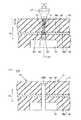
図1(a)は、レーザー光LA1を照射することにより脆弱部(W1,W2)を形成する様子を模式的に例示する垂直断面図である。図1(b)は、基板(10,50)を脆弱部(W1,W2)に沿って分割した様子を模式的に例示する垂直断面図である。図2は、本製造方法により得られる液体噴射ヘッドの一例である記録ヘッド1の要部を便宜上、分解した分解斜視図である。図3(a)は、記録ヘッド1の構成の概略を例示する平面図である。図3(b)は、図3(a)のA1−A1の位置で記録ヘッド1の1セグメントを破断した垂直断面図である。なお、基板分割後に切断部LN2近傍に残る可能性のある微細構造の図示を省略している。D1は圧力発生室12の幅方向、D2は幅方向D1と直交する圧力発生室12の長手方向、を示している。D3は、流路形成基板(第2基板)10、振動板16、保護基板(第1基板)50、等の厚み方向、すなわち、圧力発生室12の深さ方向を示している。分かり易く示すため、幅方向D1及び厚み方向D3の拡大率は長手方向D2の拡大率よりも大きくされ、各図は整合していないことがある。
なお、本明細書で説明する位置関係は、発明を説明するための例示に過ぎず、発明を限定するものではない。従って、第1電極の上以外の位置、例えば、下、左、右、等に第2電極が配置されることも、本発明に含まれる。(1) Examples of liquid jet heads obtained by this manufacturing method:
FIG. 1A is a vertical cross-sectional view schematically illustrating how weak portions (W1, W2) are formed by irradiating a laser beam LA1. FIG. 1B is a vertical cross-sectional view schematically illustrating a state in which the substrate (10, 50) is divided along the weakened portions (W1, W2). FIG. 2 is an exploded perspective view in which a main part of the
In addition, the positional relationship demonstrated in this specification is only the illustration for demonstrating invention, and does not limit invention. Accordingly, the present invention also includes the second electrode disposed at a position other than the top of the first electrode, for example, below, left, right, and the like.
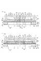
図2に例示される記録ヘッド1のチップC1は、ノズル開口71が形成されたノズルプレート70、振動板16や圧電素子3やリード電極45が形成された流路形成基板(第2基板)10、流路形成基板10の保護基板(第1基板)50、が順に積層されている。流路形成基板10には、ノズル開口71に連通する圧力発生室12、連通部13、インク供給口14、といった液体流路が形成されている。前記液体流路を流れる液体による浸食を抑制するため、図3(b)に示すように、液体流路(12〜14)の内面に保護膜80が形成されている。本記録ヘッド1は、圧力発生室12に供給する液体を貯留するリザーバ9がチップC1に外付けされている。リザーバ9は、分割されたチップC1の切断部LN2に接続されている。従って、リザーバ9内の液体は、圧力発生室の長手方向D2の外側からチップC1内に流入する。
図10に示す記録装置200に例示される液体噴射装置は、上述のような液体噴射ヘッドを備える。A chip C1 of the
The liquid ejecting apparatus exemplified in the
流路形成基板10は、膜厚が例えば500〜800μm程度と比較的厚く剛性の高いシリコン単結晶基板等から形成することができる。流路形成基板10は、セグメントSG1間が隔壁11により区画され、セグメントSG1毎の長尺な液体流路(12〜14)が形成されている。インク供給口14は、圧力発生室12及び連通部13よりも細幅とされている。各液体流路(12〜14)は、圧力発生室12の並設方向である幅方向D1へ並べられている。 The flow
振動板16は、シリコン基板15上に形成された弾性膜16aと、この弾性膜16a上に形成された絶縁膜16bとを有し、圧力発生室12の壁面の一部を構成する。弾性膜16aは例えば酸化シリコン(SiOx)で構成することができ、絶縁膜16bは例えば酸化ジルコニウム(ZrOx)で構成することができる。振動板16の厚みは、弾性を示す限り特に限定されないが、例えば0.5〜2μm程度とすることができる。The
圧電素子3は、圧電体層30と、圧電体層30の圧力発生室12側に設けられた下電極(第1電極)20と、圧電体層30の他方側に設けられた上電極(第2電極)40とを有し、圧力発生室12に圧力を印加する。圧電素子3の実質的な能動部4は、下電極20と上電極40とで圧電体層30が挟まれた領域となる。圧電素子が共通下電極構造である場合、能動部4の能動端は上電極40の境界位置となる。圧電素子が共通上電極構造である場合、能動部4の能動端は下電極20の境界位置となる。圧電素子3には、駆動IC(半導体集積回路)65に接続するために引き出されたリード電極45等が設けられている。 The
リード電極45は、振動板16上に形成された密着層46と、この密着層46上に形成された主金属層47とを有している。主金属層47の構成金属には、Au(金)、白金(Pt)、アルミニウム(Al)、銅(Cu)、これらの混合物、等を用いることができる。主金属層47の厚みは、例えば0.5〜1.5μm程度とすることができる。密着層46には、ニッケルクロム(NixCr1-x;0<x<1)、ニッケル(Ni)、クロム(Cr)、チタン(Ti)、等を用いることができる。密着層46の厚みは、例えば30〜70nm程度とすることができる。むろん、振動板16と主金属層47との密着力が十分であれば、密着層46を省略可能である。また、これらの層46,47以外の層がリード電極45に設けられてもよい。駆動IC65は、駆動配線66を介してリード電極45と電気的に接続され、並設された圧電素子3を駆動する。むろん、圧電素子3の駆動回路は、ICに限定されない。駆動配線66には、ボンディングワイヤといった導電性ワイヤ等を用いることができる。The
圧電体層30は、少なくとも圧力発生室12に対応した領域において、本質的に、下電極20の上面に形成されている。圧電体層30には、例えば、PZT(チタン酸ジルコン酸鉛、Pb(Zrx,Ti1-x)O3)といった強誘電体、これに酸化ニオブ、酸化ニッケル、酸化マグネシウム、といった金属酸化物が添加されたもの、(Bi,Ba)(Fe,Ti)O3といった非鉛系ペロブスカイト型酸化物、この酸化物のBサイトにマンガンといった金属が添加されたもの、等のペロブスカイト構造を有する材料を用いることができる。
圧電体層30の厚みは、特に限定されないが、例えば0.2〜5μm程度とすることができる。The
The thickness of the
電極(20,40)の構成金属には、Pt(白金)、Au、Ir(イリジウム)、Ti(チタン)、等の1種以上を用いることができる。構成金属は、酸化物といった化合物の状態でもよいし、化合していない状態でもよく、合金の状態でもよいし、単独の金属の状態でもよく、これらの金属を主成分としてモル比で少ない別の金属が含まれてもよい。電極(20,40)の厚みは、特に限定されないが、例えば10〜500nm程度とすることができる。 As a constituent metal of the electrodes (20, 40), one or more of Pt (platinum), Au, Ir (iridium), Ti (titanium), and the like can be used. The constituent metal may be in the state of a compound such as an oxide, in an uncombined state, in an alloy state, or in a single metal state. Metals may be included. Although the thickness of an electrode (20, 40) is not specifically limited, For example, it can be set as about 10-500 nm.
液体流路(12〜14)の内面に設けられた保護膜80には、耐液体性を有する材料が用いられている。保護膜80は、液体による流路形成基板10の浸食を抑制する。保護膜80の厚みは、特に限定されないが、例えば30〜70nm程度とすることができる。耐インク性(耐液体性の一種)を有する材料には、耐アルカリ性を有する材料が好ましい。このような材料は、五酸化二タンタル(化学量論比Ta2O5)といった酸化タンタル(TaOx)が好ましいものの、インクのpH値等に応じて酸化ジルコニウム(化学量論比ZrO2)といった金属酸化物等を用いることもできるし、酸化タンタルに他の材料(例えば金属酸化物)が含まれる材料を用いることもできる。保護膜は、単層でもよいし、酸化タンタル層と他の材料層とを積層した膜等の積層膜でもよい。A liquid-resistant material is used for the
上記流路形成基板10には、例えば接着剤55によって保護基板50が接合されている。保護基板50は、圧電素子3の上方にあって流路形成基板10、特に、振動板16上の圧電素子を保護する封止板といえる。圧電素子3に対向する領域に形成された圧電素子保持部52は、圧電素子3の運動を阻害しない程度の空間を有する。保護基板50には、例えば、シリコン単結晶基板、ガラス、セラミックス材料、金属、樹脂、等を用いることができる。シリコン基板を用いる場合、表面に酸化シリコン(SiOx)層を形成してもよい。保護基板50の厚みは、特に限定されないが、例えば100〜800μm程度とすることができる。保護基板50の接合面50aとは反対側の面が予めドライポリッシュ加工といった研磨等により鏡面化されると、保護基板50に照射されるレーザー光LA1が保護基板50の表面で乱反射するのを抑制することができる。従って、鏡面化処理により、レーザー光LA1による加工を高精度に行うことができる。A
ノズルプレート70は、各圧力発生室12のインク供給口14とは反対側の端部近傍に連通するノズル開口71が穿設され、流路形成基板10の保護膜80側の面に接着剤や熱溶着フィルムといった固定手段で固定されている。従って、圧力発生室12は、液体を吐出するノズル開口71に連通している。ノズルプレート70は、ガラスセラミックス、シリコン単結晶基板、ステンレス鋼、等を用いることができ、流路形成基板10の開口面側に固着されている。ノズルプレート70の厚みは、特に限定されないが、例えば0.01〜1mm程度とすることができる。 The
図2,3に示すリザーバ9は、リザーバ底面部材110、リザーバ天井部材120、コンプライアンス基板60、を有している。リザーバ底面部材110は、シリコン単結晶基板、ニッケルを42%含有する鉄合金(42アロイ)、等を用いることができ、リザーバ9の底面を構成する。リザーバ天井部材120は、天井壁121と3つの側壁を有し、保護基板50上に例えば接着剤を介して設けられている。天井壁121には、液体を導入するための液体導入孔122が設けられている。コンプライアンス基板60は、リザーバ天井部材120の開放された側面側にリザーバ底面部材110までに亘って接合されている。コンプライアンス基板60に設けられた封止膜61は、例えば厚み4〜8μm程度のポリフェニレンサルファイド(PPS)フィルム)といった剛性が低く可撓性を有する材料等が用いられ、リザーバ9の一方の面を封止する。コンプライアンス基板60に設けられた固定板62は、例えば厚み20〜40μm程度のステンレス鋼(SUS)といった金属等の硬質の材料が用いられ、リザーバ9に対向する領域が開口部63とされている。
むろん、リザーバ9を基板に外付けする構造は、上述した構造に限定されない。The
Of course, the structure for attaching the
ところで、図11に示す比較例のように、切断予定部LN1の振動板16上に金属膜無く保護基板50が接着剤55で接合されている場合、保護基板50に集光点P1を合わせたレーザー光LA1は振動板16を透過する。そもそも、弾性膜16aを構成する酸化シリコンと絶縁膜16bを構成する酸化ジルコニウムは、透明材料であり、レーザー光が透過する性質を有している。切断予定部LN1に残された酸化シリコン及び酸化ジルコニウムは、保護基板50に集光点P1を合わせたレーザー光LA1によっては脆弱部とならない。このため、流路形成基板10及び保護基板50にエキスパンドブレーク等の外力を加えたときに、基板(10,50)が保護基板50の脆弱部に沿って分割されないことがある。一方、切断予定部LN1の振動板16を切断したり除去したりするためには、ブレーキング等の別工程が必要となる。切断予定部LN1の絶縁膜16bを予め除去しておいたとしても、切断予定部LN1の酸化シリコン上に金属膜無く保護基板50が接合されていれば、この酸化シリコンは、保護基板50に集光点P1を合わせたレーザー光LA1によっては脆弱部とならない。従って、外力を加えた基板(10,50)が保護基板50の脆弱部に沿って分割されないことがある。なお、始めから振動板16全体を除去することはできない。これは、始めから流路形成基板10を分割することになり、分割された流路形成基板同士が保持されないためである。 By the way, as in the comparative example shown in FIG. 11, when the
本製造方法は、図1(a)に示すように、基板(10,50)の接合面(10aと50aの少なくとも一方)の少なくとも切断予定部LN1に金属膜48を形成している。基板にリザーバ9を外付けする場合、流路形成基板10のリザーバ9側の縁部は圧電素子3の駆動IC65に接続するためのリード電極を設けることができないため、金属膜48は前記リード電極とは異なる。そのうえで、流路形成基板10に接合された保護基板50の切断予定部LN1に集光点P1を合わせたレーザー光LA1を保護基板50側から照射している。これにより、保護基板50に第1脆弱部W1が形成されるとともに、切断予定部LN1の金属膜48が融解する。この段階の保護基板50は、第1脆弱部W1で繋がっており、分割されていない。また、流路形成基板10の切断予定部LN1がレーザー光LA1を透過させる材料で形成されていても、切断予定部LN1の金属膜48が融解することにより、流路形成基板10に第2脆弱部W2が形成される。これにより、後の分割工程で基板(50,10)を脆弱部(W1,W2)に沿って容易に分割することができる。 In this manufacturing method, as shown in FIG. 1A, the
第1脆弱部W1は、例えば、保護基板50(例えばシリコン単結晶基板)に対して透過特性を示す波長のレーザー光をレンズ光学系で保護基板50内の切断予定部LN1に焦点を結ぶように集光させ、集光点P1を改質することにより形成することができる。透過特性を示す波長は、溶融切断用などの吸収特性を示す波長よりも長波長側である。これにより、レーザー光LA1照射時に保護基板50は切断予定部LN1で脆弱化されるだけで切断されない。第1脆弱部W1は、溶融後多結晶化した溶融処理領域等の強度が弱められた改質領域をいう。第1脆弱部W1は、保護基板50の表層(接合面側と反対面側の少なくとも一方)を残して形成されてもよい。なお、第1脆弱部W1を形成する際に、第1脆弱部W1の一部が剥がれ落ちる場合もあるが、特に問題はない。 For example, the first fragile portion W1 focuses a laser beam having a wavelength exhibiting transmission characteristics with respect to the protective substrate 50 (for example, a silicon single crystal substrate) on the planned cutting portion LN1 in the
レーザー光LA1による保護基板50の改質は、集光点P1及びその近傍に集中して行われる。そこで、図9に示すように、切断予定部LN1で集光点P1の深さを変えて複数回レーザー光LA1を所定速度で走査させることによって第1脆弱部W1を形成してもよい。図9は、保護基板50の表層に連結部51を残す例を示している。 The modification of the
ここで、図1(a)に示すように、レーザー光LA1の保護基板50への入射幅をW、保護基板50内のレーザー光LA1の入射角度をθとすると、集光点P1の深さZは、
Z=W/(2×tanθ) …(1)
となる。従って、レーザー光の入射幅Wを調整することにより、集光点P1の深さ、すなわち、加工深さを調節することができる。Here, as shown in FIG. 1A, when the incident width of the laser beam LA1 to the
Z = W / (2 × tan θ) (1)
It becomes. Therefore, the depth of the condensing point P1, that is, the processing depth can be adjusted by adjusting the incident width W of the laser beam.
保護基板50の切断予定部LN1に集光点P1を合わせたレーザー光LA1を保護基板50側から照射すると、レーザー光LA1に対して非透過特性を示す金属膜48が融解する。金属膜48の材料は上記レーザー光LA1に対して熱吸収特性を示す材料であればよく、金属膜48の構成金属には、ニッケルクロム、ニッケル(Ni)、クロム(Cr)、チタン(Ti)、Au(金)、白金(Pt)、アルミニウム(Al)、銅(Cu)、その他の非透明材料、これらの混合物、等を用いることができる。金属膜48は、例えば30〜70nm程度と比較的薄い厚みが好ましい。なお、保護基板の切断予定部に集光点を合わせたレーザー光の照射によって金属膜48が切断予定部LN1全体にまでは融解しない場合には、切断予定部LN1全体が融解するように金属膜48を薄くすればよい。また、金属膜48の融解により流路形成基板10が切断予定部LN1全体にまでは脆弱部(W2)が形成されてない場合には、切断予定部LN1全体に脆弱部が形成されるように金属膜48を厚くすればよい。 When the laser beam LA1 in which the condensing point P1 is aligned with the planned cutting portion LN1 of the
金属膜48の材料にニッケルクロム等リード電極の密着層46の材料と同じ材料を用いると、融解して第2脆弱部W2を形成するのに好適な薄さに金属膜48を形成することができる。また、密着層46の形成時に切断予定部LN1の金属膜48も形成することができ、液体噴射ヘッドの製造コストを低減することができる。むろん、密着層46の材料層以外の層が金属膜48に設けられてもよい。 If the same material as the material of the
また、金属膜48の材料に金などリード電極の主金属層47の材料と同じ材料を用いると、主金属層47の形成時に切断予定部LN1の金属膜48も形成することができ、液体噴射ヘッドの製造コストを低減することができる。むろん、密着層46など主金属層47の材料層以外の層が金属膜48に設けられてもよい。
さらに、金属膜48は、密着層46の形成とは別に形成されてもよい。If the same material as the material of the
Further, the
第2脆弱部W2は、融解した金属膜W3により切断予定部LN1の流路形成基板10に形成される。第2脆弱部W2は、溶融後固化した溶融領域等の強度が弱められた領域をいう。流路形成基板10の切断予定部LN1における接合面10aとは反対側の部位を除去して凹部R1を形成すると、流路形成基板10の切断予定部LN1全体に第2脆弱部W2が形成され易いので、好適である。切断予定部LN1に凹部R1を形成して振動板16を残すと、切断予定部LN1全体に第2脆弱部W2を形成するのに好適な薄さに流路形成基板10を形成することができる。凹部R1をリザーバ9への連通部13にすると、凹部R1専用の領域が不要となるので、好適である。また、流路形成基板10の切断予定部LN1から絶縁膜16bを除去した後に金属膜48を形成すると、切断予定部LN1全体に第2脆弱部W2を形成するのにさらに好適な薄さに流路形成基板10を形成することができる。
なお、融解した金属膜W3により、切断予定部LN1の接着剤55も変質して脆弱部W4となる。The second fragile portion W2 is formed on the flow
Note that, due to the melted metal film W3, the adhesive 55 of the planned cutting portion LN1 is also changed into a fragile portion W4.
(2)液体噴射ヘッドの製造方法の例:
次に、図4〜9を参照して、記録ヘッドの製造方法を例示する。図4〜9は、図2,3とは細部の構造が異なる記録ヘッド1Aを圧力発生室の長手方向D2に沿った垂直断面図で示している。まず、流路形成基板10用の例えば面方位(110)のシリコンウェハを例えば1000〜1200℃程度の拡散炉で熱酸化する等によって、シリコン基板15の表面に対して弾性膜16aを一体に形成する。弾性膜16aは、二酸化シリコン(化学量論比SiO2)等で構成することができ、例えば厚み400〜1500nm程度とすることができる。次いで、図4(a)に示すように、弾性膜16a上に絶縁膜16bを形成する。例えば、スパッタ法等によりジルコニウム(Zr)層を弾性膜16a上に形成した後にジルコニウム層を例えば500〜1200℃程度の拡散炉で熱酸化することにより、酸化ジルコニウム層を絶縁膜16bとして形成することができる。絶縁膜16bの厚みは、例えば300〜500nm程度とすることができる。図4(a)に示す例では、絶縁膜16bを形成した後にパターニングして、切断予定部LN1に貫通部16cを形成している。例えば、絶縁膜16bをエッチングすることにより、切断予定部LN1の絶縁膜16bを弾性膜16a上から除去する。なお、表面に金属膜48が形成される振動板16の概念には、絶縁膜16bを除去した弾性膜16aも含まれるものとする。
以上が、振動板形成工程S1である。(2) Example of manufacturing method of liquid jet head:
Next, with reference to FIGS. 4 to 9, a method for manufacturing a recording head is illustrated. 4 to 9 show a
The above is the diaphragm forming step S1.
次いで、スパッタ法等によって振動板16上に下電極20を形成する。図4(b)に示す例では、下電極20を形成した後にパターニングしている。なお、上述した酸化ジルコニウム層の代わりに、又は、酸化ジルコニウム層に加えて、窒化チタンアルミ(TiAlN)膜、Ir膜、酸化イリジウム(IrO)膜、等の層を密着層又は拡散防止層として振動板16上に形成したうえで、当該層上に下電極20を形成してもよい。 Next, the
次いで、スピンコート法といった液相法等によって少なくとも下電極20上に圧電体層30を形成し、スパッタ法等によって少なくとも圧電体層30上に上電極40を形成する。図4(b)に示す例では、上電極40を形成した後に圧電体層30及び上電極40をパターニングしている。これにより、圧電体層30及び電極(20,40)を有する圧電素子3が形成され、この圧電素子3及び振動板16を備えた圧電アクチュエーター2が形成される。以上が、圧電素子形成工程S2である。 Next, the
圧電体層30を形成する場合、例えば、上述したPZTを構成する金属の有機物を分散媒に分散した前駆体溶液の塗布工程、例えば170〜180℃程度の乾燥工程、例えば300〜400℃程度の脱脂工程、及び、例えば550〜800℃程度の焼成工程を経ることにより、ペロブスカイト型酸化物を有する圧電体層30が形成される。塗布工程と乾燥工程と脱脂工程と焼成工程の組合せは、複数回行ってもよい。なお、液相法以外にも、スパッタ法といった気相法等で圧電体層30を形成してもよい。 When the
次いで、図4(c)に示すように、基板上に密着層46を形成する(金属膜形成工程S3)。例えば、圧電素子3を設けた基板の全面に亘ってニッケルクロム等の密着層46をスパッタ法等により形成し、レジスト等からなるマスクパターンを介してパターニングすればよい。すると、リード電極45の密着層とは不連続の金属膜48(例えばニッケルクロム層)を切断予定部LN1の弾性膜16a(例えば酸化シリコン層)上に形成することができる。この金属膜形成工程S3により、リード電極45の密着層と同時に隔離層である金属膜48を形成することができ、製造工程を簡略化してコストを低減することができる。むろん、リード電極45の密着層の形成とは別に金属膜48を形成してもよい。 Next, as shown in FIG. 4C, an
次いで、図4(d)に示すように、基板上に主金属層47を形成する(主金属層形成工程S4)。例えば、基板の全面に亘って金等の主金属層47をスパッタ法等により形成し、レジスト等からなるマスクパターンを介してパターニングすればよい。 Next, as shown in FIG. 4D, a
なお、電極(20,40)や密着層46や主金属層47は、DC(直流)マグネトロンスパッタリング法といったスパッタ法等によって形成することができる。各層の厚みは、スパッタ装置の印加電圧やスパッタ処理時間を変えることにより調整することができる。 The electrodes (20, 40), the
次いで、図5(a)に示すように、圧電素子保持部52を予め形成した保護基板50を流路形成基板10の接合面10aに例えば接着剤55によって接合する(保護基板接合工程S5)。図5(a)に示す例では、切断予定部LN1において、接合面10aに設けられた金属膜48と保護基板50の接合面50aとの間に接着剤55が存在する。 Next, as shown in FIG. 5A, the
次いで、図5(b)に示すように、弾性膜16aを形成したシリコン基板15を例えば60〜80μm程度にする。例えば、当該シリコン基板15において圧電素子3とは反対側をある程度の厚さとなるまで研磨した後、さらにフッ硝酸によってウェットエッチングすることにより所定の厚みにする(削成工程S6)。なお、流路形成基板10の振動板16とは反対側の面をノズル側面10bとする。 Next, as shown in FIG. 5B, the
次いで、図6(a)に示すように、マスクを介してKOH水溶液等のアルカリ溶液でシリコン基板15のノズル側面10bを異方性エッチング(ウェットエッチング)し、圧力発生室12やインク供給口14や凹部R1を形成する(流路形成工程S7)。例えば、シリコン基板15のノズル側面10bに窒化シリコン(化学量論比Si3N4)といったマスク膜を形成し、パターニングして圧力発生室12や凹部R1等に対応したマスク開口部を形成し、このマスク開口部を有するマスク膜を介してエッチングすると、液体流路(12,14)や凹部R1が形成される。その後、エッチングすることによりマスク膜を除去してもよい。凹部R1は、流路形成基板10の切断予定部LN1における振動板16とは反対側の除去部位であり、リザーバ9への連通部13となる部位である。
なお、液体流路は、圧電素子3の形成前に形成されてもよい。Next, as shown in FIG. 6A, the
The liquid channel may be formed before the
次いで、図6(b)に示すように、液体流路(12,14)や凹部R1の内面等に保護膜80を形成する(保護膜形成工程S8)。例えば、上述した酸化タンタルを化学気相法によりノズル側面10bから流路形成基板10に堆積させると、液体流路(12,14)や凹部R1の内面を含むノズル側面10bの全面にわたって保護膜80を形成することができる。 Next, as shown in FIG. 6B, a
次いで、図7(a)に示すように、保護基板50の切断予定部LN1に集光点P1を合わせたレーザー光LA1を保護基板50側から照射することにより、保護基板50に第1脆弱部W1を形成するとともに切断予定部LN1の金属膜48を融解させて流路形成基板10に第2脆弱部W2を形成する(脆弱部形成工程S9)。例えば、図9に示すように、切断予定部LN1で集光点P1の深さを変えて複数回レーザー光LA1を走査させ、厚み方向D3に沿って第1脆弱部W1を形成する。上述したように、第1脆弱部W1は強度が弱められた改質領域であるため、保護基板50は、第1脆弱部W1で繋がっており、分割されていない。また、融解した金属膜W3により、切断予定部LN1の接着剤55も脆弱部W4となる。 Next, as shown in FIG. 7A, the first weakened portion is applied to the
次いで、図7(b)に示すように、接合された基板(50,10)を脆弱部(W1,W2)に沿ってエキスパンドブレーク等により分割する(分割工程S10)。エキスパンドブレークの場合、例えば、ダイシング用粘着テープを基板の一面に貼り、この粘着テープを縦横に引き伸ばす外力を基板に加えて切断予定部LN1を切断する。これにより、切断予定部LN1で複数のチップC1に分離することができる。 Next, as shown in FIG. 7B, the bonded substrates (50, 10) are divided along an fragile portion (W1, W2) by an expand break or the like (dividing step S10). In the case of an expanding break, for example, a dicing adhesive tape is applied to one surface of the substrate, and an external force that stretches the adhesive tape vertically and horizontally is applied to the substrate to cut the planned cutting portion LN1. Thereby, it is separable into the some chip | tip C1 by the cutting plan part LN1.
次いで、図8(a),(b)に示すように、各チップC1の主金属層47(リード電極45)と駆動IC65とを駆動配線66によって接続し、ノズル開口71を有するノズルプレート70を各チップC1の圧力発生室12側の面に接合し、切断部LN2にリザーバ9を外付けする(リザーバ形成工程S11)。流路形成基板10の開口面側に対するノズルプレート70の固着には、接着剤、熱溶着フィルム、等を用いることができる。リザーバ9は、ノズルプレート70を接合したチップC1に、リザーバ底面部材110と、液体導入孔122を有するリザーバ天井部材120と、封止膜61及び固定板62を積層したコンプライアンス基板60とを接合することにより形成される。分割された凹部R1は、リザーバ9の連通部13として機能する。ノズルプレート70の圧力発生室12とは反対側の面に対するリザーバ底面部材110の固着にも、接着剤、熱溶着フィルム、等を用いることができる。保護基板50の接合面50aとは反対側の面に対するリザーバ天井部材120の固着にも、接着剤、熱溶着フィルム、等を用いることができる。これらの部材(110,120)に対するコンプライアンス基板60の固着にも、接着剤、熱溶着フィルム、等を用いることができる。
以上により、記録ヘッド1Aが製造される。Next, as shown in FIGS. 8A and 8B, the main metal layer 47 (lead electrode 45) of each chip C1 and the driving
Thus, the
本記録ヘッド1Aは、図示しない外部インク供給手段と接続した液体導入孔122からインクを取り込み、リザーバ9からノズル開口71に至るまで内部をインクで満たす。駆動IC65からの記録信号に従い、圧力発生室12毎に下電極20と上電極40との間に電圧を印加すると、圧電体層30、下電極20及び振動板16の変形によりノズル開口71からインク滴が吐出する。 The
一実施例として、以下のサンプルを作製した。
上述した製造方法に従って、面方位(110)の流路形成基板用シリコン単結晶基板の表面に酸化シリコン(化学量論比SiO2)の弾性膜16aを形成した。該弾性膜上に、貫通部16cを有する酸化ジルコニウム(化学量論比ZrO2)の絶縁膜16b、PZTの圧電体層30を有する圧電素子3、ニッケルクロムの密着層46(金属膜48を含む。)、及び、金の主金属層47を形成した。ニッケルクロム層は、レーザー光LA1の照射による融解により切断予定部LN1の流路形成基板10が脆弱部(W2)に変質するような厚みに設定した。また、面方位(110)の保護基板用シリコン単結晶基板の表面に酸化シリコン層を形成し、該基板に圧電素子保持部52を形成して、流路形成基板10と保護基板50とを接着剤55で接合した。接合後の流路形成基板10のノズル側面10bに液体流路(12,14)及び凹部R1を形成し、ノズル側面10bの全面にわたって酸化タンタル(化学量論比Ta2O5)の保護膜80を形成した。その後、保護基板50の切断予定部LN1に集光点P1を合わせたシリコン透過性のレーザー光LA1を保護基板50側から照射することにより、保護基板50のシリコンに第1脆弱部W1を形成した。As an example, the following sample was prepared.
In accordance with the manufacturing method described above, an
また、一比較例として、図11で示した構造のサンプルを作製した。比較例サンプルは、切断予定部LN1において、切断予定部LN1の酸化ジルコニウム層上に金属膜無く保護基板50が接着剤55で接合されている。 As a comparative example, a sample having the structure shown in FIG. 11 was produced. In the comparative sample, in the planned cutting portion LN1, the
それぞれのサンプルについて、基板の断面を観察した。接合面に金属膜を形成しなかった比較例サンプルは、流路形成基板10の切断予定部LN1にある酸化シリコン層及び酸化ジルコニウム層に脆弱部が形成されていないことが確認された。切断予定部LN1の接着剤55も、脆弱部となっていなかった。一方、接合面に金属膜を形成した実施例サンプルは、切断予定部LN1のニッケルクロムが融解し、流路形成基板10の切断予定部LN1にある酸化シリコン、酸化ジルコニウム、及び、酸化タンタルが変質している(第2脆弱部W2が形成されている)ことが確認された。切断予定部LN1の接着剤55も、変質している(脆弱部W4が形成されている)ことが確認された。 About each sample, the cross section of the board | substrate was observed. In the comparative sample in which the metal film was not formed on the bonding surface, it was confirmed that no fragile portion was formed in the silicon oxide layer and the zirconium oxide layer in the planned cutting portion LN1 of the flow
また、それぞれのサンプルについて、ダイシング用粘着テープを基板の一面に貼り、この粘着テープを縦横に引き伸ばして基板の分割を試みた。比較例サンプルは、切断予定部LN1で分割されないチップが生じた。一方、実施例サンプルは、容易に切断予定部LN1で複数のチップに分割された。 Moreover, about each sample, the adhesive tape for dicing was affixed on the one surface of this board | substrate, and this adhesive tape was extended vertically and horizontally and the division | segmentation of the board | substrate was tried. In the comparative sample, chips that were not divided at the planned cutting portion LN1 were generated. On the other hand, the example sample was easily divided into a plurality of chips at the planned cutting portion LN1.
以上より、本製造方法は、流路形成基板の切断予定部がレーザー光を透過させる材料で形成されていても、切断予定部の金属膜が融解することにより、流路形成基板に第2脆弱部を形成することができる。これにより、後の分割工程で保護基板及び流路形成基板を第1脆弱部及び第2脆弱部に沿って容易に分割することができる。従って、本製造方法は、切断予定部の振動板を切断したり除去したりする等の別工程が不要であり、液体噴射ヘッドの製造工程を簡略化することができる。As described above, even if the planned cutting portion of the flow path forming substrate is formed of a material that transmits laser light, the manufacturing method has a second weakness in the flow path forming substrate because the metal film of the planned cutting portion melts. The part can be formed. Thereby, a protection board and a channel formation substrate can be easily divided along the 1st weak part and the 2nd weak part by a subsequent division process. Therefore, this manufacturing method does not require a separate process such as cutting or removing the diaphragm of the planned cutting part, and can simplify the manufacturing process of the liquid jet head.
(3)液体噴射装置:
図10は、上述した記録ヘッド1(1Aを含む。)を有するインクジェット式の記録装置(液体噴射装置)200の外観を示している。記録ヘッド1を記録ヘッドユニット211,212に組み込むと、耐久性を向上させた記録装置200を製造することができる。図10に示す記録装置200は、記録ヘッドユニット211,212のそれぞれに、記録ヘッド1が設けられ、外部インク供給手段であるインクカートリッジ221,222が着脱可能に設けられている。記録ヘッドユニット211,212を搭載したキャリッジ203は、装置本体204に取り付けられたキャリッジ軸205に沿って往復移動可能に設けられている。駆動モーター206の駆動力が図示しない複数の歯車及びタイミングベルト207を介してキャリッジ203に伝達されると、キャリッジ203がキャリッジ軸205に沿って移動する。図示しない給紙ローラー等により給紙される記録シート290は、プラテン208上に搬送され、インクカートリッジ221,222から供給され記録ヘッド1から吐出するインクにより印刷がなされる。(3) Liquid ejecting apparatus:
FIG. 10 shows an appearance of an ink jet recording apparatus (liquid ejecting apparatus) 200 having the above-described recording head 1 (including 1A). When the
(4)応用、その他:
本発明は、種々の変形例が考えられる。
上述した製造工程の順序は、適宜、変更可能である。例えば、振動板形成工程S1で振動板16を形成した後、金属膜48を形成してから圧電素子3を形成してもよい。
上述した実施形態では圧力発生室毎に個別の圧電体を設けているが、複数の圧力発生室に共通の圧電体を設け圧力発生室毎に個別電極を設けることも可能である。
上述した実施形態では圧電素子の上側を圧電素子保持部で覆っているが、圧電素子の上側を大気に開放することも可能である。(4) Application and others:
Various modifications can be considered for the present invention.
The order of the manufacturing processes described above can be changed as appropriate. For example, the
In the above-described embodiment, an individual piezoelectric body is provided for each pressure generation chamber. However, a common piezoelectric body may be provided for a plurality of pressure generation chambers, and an individual electrode may be provided for each pressure generation chamber.
In the above-described embodiment, the upper side of the piezoelectric element is covered with the piezoelectric element holding unit, but the upper side of the piezoelectric element can be opened to the atmosphere.
流体噴射ヘッドから吐出される液体は、液体噴射ヘッドから吐出可能な材料であればよく、染料等が溶媒に溶解した溶液、顔料や金属粒子といった固形粒子が分散媒に分散したゾル、等の流体が含まれる。このような流体には、インク、液晶、等が含まれる。液体噴射ヘッドは、プリンターといった画像記録装置の他、液晶ディスプレー等のカラーフィルタの製造装置、有機ELディスプレー等の電極の製造装置、バイオチップ製造装置、等に搭載可能である。
なお、従属請求項に係る構成要件を有しておらず独立請求項に係る構成要件のみからなる製造方法等でも、上述した基本的な作用、効果が得られる。The liquid ejected from the fluid ejecting head may be any material that can be ejected from the liquid ejecting head, such as a solution in which a dye or the like is dissolved in a solvent, or a sol in which solid particles such as pigments or metal particles are dispersed in a dispersion medium. Is included. Such fluids include ink, liquid crystal, and the like. The liquid ejecting head can be mounted on an image recording apparatus such as a printer, a color filter manufacturing apparatus such as a liquid crystal display, an electrode manufacturing apparatus such as an organic EL display, a biochip manufacturing apparatus, and the like.
Note that the above-described basic actions and effects can also be obtained by a manufacturing method or the like that does not have the constituent requirements according to the dependent claims but includes only the constituent requirements according to the independent claims.
以上説明したように、本発明によると、種々の態様により、チップの製造工程を簡略化することができる技術等を提供することができる。
また、上述した実施形態及び変形例の中で開示した各構成を相互に置換したり組み合わせを変更したりした構成、公知技術並びに上述した実施形態及び変形例の中で開示した各構成を相互に置換したり組み合わせを変更したりした構成、等も実施可能である。本発明は、これらの構成等も含まれる。As described above, according to the present invention, a technique or the like that can simplify the chip manufacturing process can be provided according to various aspects.
In addition, the configurations disclosed in the embodiments and modifications described above are mutually replaced, the combinations are changed, the known technology, and the configurations disclosed in the embodiments and modifications described above are mutually connected. It is possible to implement a configuration in which replacement or combination is changed. The present invention includes these configurations and the like.
1,1A…記録ヘッド(液体噴射ヘッド)、2…圧電アクチュエーター、3…圧電素子、9…リザーバ、10…流路形成基板(第2基板)、10a…接合面、10b…ノズル側面、12…圧力発生室、13…連通部、15…シリコン基板、16…振動板、16a…弾性膜、16b…絶縁膜、16c…貫通部、20…下電極(第1電極)、30…圧電体層、40…上電極(第2電極)、45…リード電極、46…密着層、47…主金属層、48…金属膜、50…保護基板(第1基板)、50a…接合面、51…連結部、55…接着剤、60…コンプライアンス基板、65…駆動IC、70…ノズルプレート、71…ノズル開口、80…保護膜、110…リザーバ底面部材、120…リザーバ天井部材、200…記録装置(液体噴射装置)、C1…チップ、LA1…レーザー光、LN1…切断予定部、LN2…切断部、P1…集光点、R1…凹部、S1…振動板形成工程、S2…圧電素子形成工程、S3…金属膜形成工程、S4…主金属層形成工程、S5…保護基板接合工程、S6…削成工程、S7…流路形成工程、S8…保護膜形成工程、S9…脆弱部形成工程、S10…分割工程、S11…リザーバ形成工程、W1…第1脆弱部、W2…第2脆弱部、W3…融解した金属膜、W4…接着剤の脆弱部。DESCRIPTION OF
Claims (7)
Translated fromJapanese前記圧力発生室の壁面の一部を構成する振動板を前記流路形成基板の接合面に形成する工程と、
前記流路形成基板と前記保護基板との接合面の少なくとも前記切断予定部に金属膜を形成する工程と、
前記切断予定部に集光点を合わせたレーザー光を前記保護基板側から照射することにより、該保護基板に第1脆弱部を形成するとともに前記切断予定部の金属膜を融解させて前記流路形成基板に第2脆弱部を形成する脆弱部形成工程と、
前記保護基板と前記流路形成基板とを前記第1脆弱部と前記第2脆弱部とに沿って分割する分割工程と、を含み、
前記流路形成基板の前記圧電素子とは反対側の面に前記圧力発生室を形成するととともに前記流路形成基板の前記切断予定部における前記保護基板とは反対側の部位を除去し、前記圧力発生室、及び、前記除去した部位の内面に耐液体性を有する保護膜を形成した後、前記脆弱部形成工程を行うことを特徴とする、液体噴射ヘッドの製造方法。A flow path forming substrate having a piezoelectric element for applying a pressure to the pressure generating chamberand pressure generating chamber communicating with a nozzleopening, joined to the passage forming substrate be inopposite to the pressure generating chamber from the piezoelectric element A method for manufacturing a liquid jet head, comprising a step of separating the protective substrateat a scheduled cutting portion,
Forming a diaphragm constituting a part of the wall surface of the pressure generating chamber on the joint surface of the flow path forming substrate;
Forming a metal film on at least the planned cutting portion of the joint surface between the flow path forming substrate and the protective substrate;
By irradiating a laser beam with its focusing point tothe cut portion from the protective substrate side, the flow path to melt the metal film of the cut portion to form a first fragile portion in the protective substrate A fragile portion forming step of forming a second fragile portion on the forming substrate;
Seen including a dividing step of dividing alongthefront Symbol protective substrateand the flow path forming substrateand the second weak portionand the first weakportion,
Forming the pressure generating chamber on a surface of the flow path forming substrate opposite to the piezoelectric element, and removing a portion of the flow path forming substrate opposite to the protective substrate in the scheduled cutting portion; A method of manufacturing a liquid ejecting head, wherein the weakened portion forming step is performed after forming a protective film having liquid resistance on the inner surface of the generation chamber and the removed portion .
Priority Applications (2)
| Application Number | Priority Date | Filing Date | Title |
|---|---|---|---|
| JP2012098104AJP6011002B2 (en) | 2012-04-23 | 2012-04-23 | Manufacturing method of liquid ejecting head and manufacturing method of liquid ejecting apparatus |
| US13/850,105US9375930B2 (en) | 2012-04-23 | 2013-03-25 | Chip manufacturing method and liquid ejecting head manufacturing method |
Applications Claiming Priority (1)
| Application Number | Priority Date | Filing Date | Title |
|---|---|---|---|
| JP2012098104AJP6011002B2 (en) | 2012-04-23 | 2012-04-23 | Manufacturing method of liquid ejecting head and manufacturing method of liquid ejecting apparatus |
Publications (2)
| Publication Number | Publication Date |
|---|---|
| JP2013223997A JP2013223997A (en) | 2013-10-31 |
| JP6011002B2true JP6011002B2 (en) | 2016-10-19 |
Family
ID=49378768
Family Applications (1)
| Application Number | Title | Priority Date | Filing Date |
|---|---|---|---|
| JP2012098104AActiveJP6011002B2 (en) | 2012-04-23 | 2012-04-23 | Manufacturing method of liquid ejecting head and manufacturing method of liquid ejecting apparatus |
Country Status (2)
| Country | Link |
|---|---|
| US (1) | US9375930B2 (en) |
| JP (1) | JP6011002B2 (en) |
Families Citing this family (3)
| Publication number | Priority date | Publication date | Assignee | Title |
|---|---|---|---|---|
| JP6750279B2 (en)* | 2016-03-31 | 2020-09-02 | ブラザー工業株式会社 | Liquid ejector |
| JP6897089B2 (en) | 2016-12-21 | 2021-06-30 | セイコーエプソン株式会社 | MEMS device, liquid injection head, liquid injection device, method for manufacturing MEMS device, method for manufacturing liquid injection head, and method for manufacturing liquid injection device. |
| JP7310133B2 (en)* | 2018-12-26 | 2023-07-19 | セイコーエプソン株式会社 | liquid injection unit |
Family Cites Families (17)
| Publication number | Priority date | Publication date | Assignee | Title |
|---|---|---|---|---|
| US6168263B1 (en)* | 1990-09-21 | 2001-01-02 | Seiko Epson Corporation | Ink jet recording apparatus |
| IT1320381B1 (en)* | 2000-05-29 | 2003-11-26 | Olivetti Lexikon Spa | METHOD FOR THE MANUFACTURE OF AN EJECTION HEAD OF DILQUID DROPS, PARTICULARLY SUITABLE FOR OPERATING WITH CHEMICALLY LIQUIDS |
| JP4659300B2 (en)* | 2000-09-13 | 2011-03-30 | 浜松ホトニクス株式会社 | Laser processing method and semiconductor chip manufacturing method |
| EP2400539B1 (en)* | 2002-03-12 | 2017-07-26 | Hamamatsu Photonics K.K. | Substrate dividing method |
| JP3825753B2 (en)* | 2003-01-14 | 2006-09-27 | 株式会社東芝 | Manufacturing method of semiconductor device |
| US7008861B2 (en)* | 2003-12-11 | 2006-03-07 | Cree, Inc. | Semiconductor substrate assemblies and methods for preparing and dicing the same |
| JP2005268752A (en)* | 2004-02-19 | 2005-09-29 | Canon Inc | Laser cleaving method, member to be cleaved, and semiconductor element chip |
| JP2006147623A (en)* | 2004-11-16 | 2006-06-08 | Tdk Corp | Cutting process of wafer |
| JP2006270009A (en)* | 2005-02-25 | 2006-10-05 | Seiko Epson Corp | Manufacturing method of electronic device |
| JP2006286727A (en)* | 2005-03-31 | 2006-10-19 | Denso Corp | Semiconductor wafer provided with plurality of semiconductor devices and its dicing method |
| JP2006281605A (en)* | 2005-03-31 | 2006-10-19 | Seiko Epson Corp | Method for manufacturing liquid jet head |
| WO2007055010A1 (en)* | 2005-11-10 | 2007-05-18 | Renesas Technology Corp. | Semiconductor device manufacturing method and semiconductor device |
| JP4923874B2 (en)* | 2005-11-16 | 2012-04-25 | 株式会社デンソー | Semiconductor wafer |
| JP2007317747A (en)* | 2006-05-23 | 2007-12-06 | Seiko Epson Corp | Substrate dividing method and liquid jet head manufacturing method |
| JP4306717B2 (en)* | 2006-11-09 | 2009-08-05 | セイコーエプソン株式会社 | Method for manufacturing silicon device and method for manufacturing liquid jet head |
| JP5440055B2 (en)* | 2009-09-15 | 2014-03-12 | セイコーエプソン株式会社 | Liquid ejecting head and liquid ejecting apparatus |
| JP2011121817A (en)* | 2009-12-10 | 2011-06-23 | Seiko Instruments Inc | Method for cutting joined glass, method for manufacturing package, package, piezoelectric vibrator, oscillator, electronic equipment and radio-controlled clock |
- 2012
- 2012-04-23JPJP2012098104Apatent/JP6011002B2/enactiveActive
- 2013
- 2013-03-25USUS13/850,105patent/US9375930B2/enactiveActive
Also Published As
| Publication number | Publication date |
|---|---|
| JP2013223997A (en) | 2013-10-31 |
| US9375930B2 (en) | 2016-06-28 |
| US20130276277A1 (en) | 2013-10-24 |
Similar Documents
| Publication | Publication Date | Title |
|---|---|---|
| JP4258668B2 (en) | Liquid ejecting head and liquid ejecting apparatus | |
| JP6011002B2 (en) | Manufacturing method of liquid ejecting head and manufacturing method of liquid ejecting apparatus | |
| JP5098656B2 (en) | Method for manufacturing liquid jet head | |
| JP2009214522A (en) | Liquid jet head, method of manufacturing liquid jet head, and liquid jet device | |
| US7402256B2 (en) | Method for producing liquid-jet head | |
| JP2019217706A (en) | Liquid jet head, and liquid jet device | |
| JP6102081B2 (en) | Manufacturing method of liquid ejecting head and manufacturing method of liquid ejecting apparatus | |
| JP2009233870A (en) | Liquid jetting head and liquid jetting apparatus | |
| JP5453585B2 (en) | Liquid ejecting head, liquid ejecting head unit, and liquid ejecting apparatus | |
| JP5088487B2 (en) | Liquid ejecting head and manufacturing method thereof | |
| JP2009061729A (en) | Liquid ejecting head and liquid ejecting apparatus | |
| JP4591005B2 (en) | Method for manufacturing liquid jet head | |
| JP5754498B2 (en) | Liquid ejecting head, liquid ejecting head unit, and liquid ejecting apparatus | |
| JP5157127B2 (en) | Actuator device, manufacturing method thereof, liquid jet head, and liquid jet device | |
| JP4821982B2 (en) | Method for manufacturing liquid jet head | |
| JP2008073961A (en) | Liquid ejecting head manufacturing method, liquid ejecting head, and liquid ejecting apparatus | |
| JP2013146911A (en) | Method for manufacturing liquid ejection head, and method for manufacturing liquid ejection device | |
| JP2009220507A (en) | Method for manufacturing liquid ejection head | |
| JP4433787B2 (en) | Liquid ejecting head, manufacturing method thereof, and liquid ejecting apparatus | |
| JP5849730B2 (en) | Manufacturing method of liquid ejecting head and manufacturing method of liquid ejecting apparatus | |
| JP2007176030A (en) | Method for manufacturing liquid jet head | |
| JP4877507B2 (en) | Method for manufacturing liquid jet head | |
| JP2010125682A (en) | Liquid jet head | |
| JP2008200905A (en) | Method for manufacturing liquid jet head | |
| JP2009154432A (en) | Liquid jet head and manufacturing method thereof |
Legal Events
| Date | Code | Title | Description |
|---|---|---|---|
| A621 | Written request for application examination | Free format text:JAPANESE INTERMEDIATE CODE: A621 Effective date:20150325 | |
| A977 | Report on retrieval | Free format text:JAPANESE INTERMEDIATE CODE: A971007 Effective date:20160217 | |
| A131 | Notification of reasons for refusal | Free format text:JAPANESE INTERMEDIATE CODE: A131 Effective date:20160301 | |
| A521 | Request for written amendment filed | Free format text:JAPANESE INTERMEDIATE CODE: A523 Effective date:20160420 | |
| TRDD | Decision of grant or rejection written | ||
| A01 | Written decision to grant a patent or to grant a registration (utility model) | Free format text:JAPANESE INTERMEDIATE CODE: A01 Effective date:20160823 | |
| A61 | First payment of annual fees (during grant procedure) | Free format text:JAPANESE INTERMEDIATE CODE: A61 Effective date:20160905 | |
| R150 | Certificate of patent or registration of utility model | Ref document number:6011002 Country of ref document:JP Free format text:JAPANESE INTERMEDIATE CODE: R150 |