JP6009041B2 - Light emitting device, light emitting device unit, and light emitting device package - Google Patents
Light emitting device, light emitting device unit, and light emitting device packageDownload PDFInfo
- Publication number
- JP6009041B2 JP6009041B2JP2015115124AJP2015115124AJP6009041B2JP 6009041 B2JP6009041 B2JP 6009041B2JP 2015115124 AJP2015115124 AJP 2015115124AJP 2015115124 AJP2015115124 AJP 2015115124AJP 6009041 B2JP6009041 B2JP 6009041B2
- Authority
- JP
- Japan
- Prior art keywords
- layer
- light emitting
- electrode layer
- contact
- emitting device
- Prior art date
- Legal status (The legal status is an assumption and is not a legal conclusion. Google has not performed a legal analysis and makes no representation as to the accuracy of the status listed.)
- Active
Links
Images


Landscapes
- Led Device Packages (AREA)
- Led Devices (AREA)
Description
Translated fromJapaneseこの発明は、発光素子、これを含む発光素子ユニットおよび発光素子ユニットを樹脂パッケージで覆った発光素子パッケージに関する。 The present invention relates to a light emitting element, a light emitting element unit including the light emitting element, and a light emitting element package in which the light emitting element unit is covered with a resin package.
1つの先行技術に係る半導体発光素子は、特許文献1に開示されている。この半導体発光素子では、光が取り出されるサファイア基板上にn−GaN層が積層されている。n−GaN層上には、発光層が積層されており、発光層上には、さらに、p−GaN層、反射電極、p電極、バリア層およびAuSn層が、サファイア基板側からこの順番で積層されている。一方、p−GaN層および発光層の端部領域が部分的に除去されてn−GaN層の端部領域が露出させられ、この露出したn−GaN層の端部領域上に、発光層から分離絶縁された状態で、n電極が積層されている。n電極上には、バリア層およびAuSn層が、サファイア基板側からこの順番で積層されている。n電極上のAuSn層およびp電極上のAuSn層のそれぞれは、配線基板に接合される。この状態でn電極とp電極との間に電圧が印加されると、発光層から光が発生してサファイア基板から取り出される。 A semiconductor light emitting device according to one prior art is disclosed in
特許文献1の半導体発光素子のようにn電極をn−GaN層上に直接積層する構成では、n電極とn−GaN層との接触抵抗を低減するために当該接触部分を大きくする必要がある。そこで、n−GaN層上においてn電極を配置するためのスペースをある程度の広さで確保しなければならない。これにより、発光層を配置できる領域が浸食されて狭くなってしまう。そのため、発光層を大きくすることができないので、発光効率の向上を図ることが困難である。 In the configuration in which the n electrode is directly stacked on the n-GaN layer as in the semiconductor light emitting device of
しかも、本願発明者の研究によれば、p電極とn電極との間の最短経路を通って電流が流れようとするため、n電極が端部領域に形成されている特許文献1の構造では、電流を十分に分散させることができない。そのため、n電極の近傍の領域が発光するだけで、発光層全体を均一に光らせることができない。
この問題を解決するために、本願発明者は、端部領域および端部領域から延びる複数の枝部を有する露出したn型半導体層と、その上に配置したn電極の構造を検討した。Moreover, according to the research of the present inventor, the current tends to flow through the shortest path between the p-electrode and the n-electrode. Therefore, in the structure of
In order to solve this problem, the inventor of the present application examined the structure of an exposed n-type semiconductor layer having an end region and a plurality of branches extending from the end region, and an n electrode disposed thereon.
しかし、このような電極構造では、n電極の枝部を配置するために、発光層がさらに浸食され、発光層の面積が小さくなり、発光効率が悪くなることが分かった。より具体的には、発光層の面積縮小に伴って、発光層における電流密度が高くなるので、ドループ現象により、光出力にロスが生じる。ドループ現象とは、電流集中による発熱によって発光再結合確率が低下し、内部発光効率が悪化する現象をいう。 However, it has been found that in such an electrode structure, the light emitting layer is further eroded due to the arrangement of the branches of the n electrode, the area of the light emitting layer is reduced, and the light emission efficiency is deteriorated. More specifically, since the current density in the light emitting layer increases as the area of the light emitting layer is reduced, a loss occurs in the light output due to the droop phenomenon. The droop phenomenon is a phenomenon in which the light emission recombination probability decreases due to heat generation due to current concentration, and the internal light emission efficiency deteriorates.
そこで、この発明は、前述のような技術的課題を克服し、発光効率の向上を図ることができる発光素子、これを含む発光素子ユニットおよび発光素子ユニットを樹脂パッケージで覆った発光素子パッケージを提供する。 Accordingly, the present invention provides a light emitting device capable of overcoming the technical problems as described above and improving luminous efficiency, a light emitting device unit including the light emitting device, and a light emitting device package in which the light emitting device unit is covered with a resin package. To do.
この発明の発光素子は、第1導電型半導体層(第1導電型の半導体層)と、前記第1導電型半導体層上に積層された発光層と、前記発光層上に積層された第2導電型半導体層(前記第1導電型とは異なる第2導電型の半導体層)と、前記第2導電型半導体層上に積層され、前記発光層の発光波長に対して透明な透明電極層と、前記透明電極層上に積層され、前記透明電極層を透過した光を反射させる反射電極層と、前記反射電極層上に積層された絶縁層と、前記絶縁層上に積層された第1電極層と、前記第1電極層から分離絶縁された状態で前記絶縁層上に積層された第2電極層と、前記第1導電型半導体層の厚さ方向から見た平面視において離散して配置されており、前記絶縁層から連続して前記反射電極層、透明電極層、第2導電型半導体層および発光層を貫通し、前記第1導電型半導体層に到達する複数の絶縁管層と、前記第1電極層から連続し、前記絶縁層および前記絶縁管層を通って前記第1導電型半導体層に接続された第1コンタクトと、前記第2電極層から連続し、前記絶縁層を貫通して前記反射電極層に接続された第2コンタクトとを含み、前記平面視において、前記発光層、前記第2導電型半導体層、前記透明電極層および前記反射電極層のそれぞれの領域が一致していて、前記絶縁層は、前記反射電極層において前記平面視で前記絶縁管層と前記第2コンタクトによる開口部とを除く全てを覆うように前記反射電極層上に積層されている(請求項1)。The light emitting device of the present invention includes a first conductive type semiconductor layer (first conductive type semiconductor layer), a light emitting layer stacked on the first conductive type semiconductor layer, and a second stacked on the light emitting layer. A conductive semiconductor layer (a second conductive type semiconductor layer different from the first conductive type), a transparent electrode layer laminated on the second conductive type semiconductor layer, and transparent to the emission wavelength of the light emitting layer; A reflective electrode layer that is laminated on the transparent electrode layer and reflects light transmitted through the transparent electrode layer; an insulating layer that is laminated on the reflective electrode layer; and a first electrode that is laminated on the insulating layer A layer, a second electrode layer stacked on the insulating layer in a state of being separated and insulated from the first electrode layer, and a discrete arrangement in a plan view as viewed from the thickness direction of the first conductive semiconductor layer The reflective electrode layer, the transparent electrode layer, and the second conductivity type semiconductor are continuously formed from the insulating layer. A plurality of insulating tube layers that penetrate the layers and the light emitting layer and reach the first conductive type semiconductor layer; and the first conductive type through the insulating layer and the insulating tube layer, continuous from the first electrode layer. a first contact connected to the semiconductor layer, the second continuous from the electrode layer, anda second contact connected to the reflective electrode layer through the insulating layer, beforeKitaira plane view, the The respective regions of the light emitting layer, the second conductive type semiconductor layer, the transparent electrode layer, and the reflective electrode layer are coincident with each other, and the insulating layer and the insulating tube layer in the planar view in the reflective electrode layer wherein thathave been stacked on the reflective electrode layer so as to cover all but the opening of the second contact (claim1).
「発光波長に対して透明」とは、具体的には、たとえば、発光波長の透過率が60%以上の場合をいう。
この構成によれば、絶縁層上の第1電極層は、絶縁層、反射電極層、透明電極層、第2導電型半導体層および発光層を挟んで隔てた第1導電型半導体層に対して、第1コンタクトを介して接続されている。第1コンタクトは、絶縁管層を通ることによって、反射電極層、透明電極層、第2導電型半導体層および発光層から分離絶縁されている。絶縁層上の第2電極層は、絶縁層下の反射電極層に対して、第2コンタクトを介して接続されている。Specifically, “transparent to the emission wavelength” means, for example, a case where the transmittance of the emission wavelength is 60% or more.
According to this configuration, the first electrode layer on the insulating layer is separated from the first conductive semiconductor layer with the insulating layer, the reflective electrode layer, the transparent electrode layer, the second conductive semiconductor layer, and the light emitting layer interposed therebetween. Are connected via the first contact. The first contact is separated and insulated from the reflective electrode layer, the transparent electrode layer, the second conductivity type semiconductor layer, and the light emitting layer by passing through the insulating tube layer. The second electrode layer on the insulating layer is connected to the reflective electrode layer below the insulating layer via a second contact.
第1電極層と第2電極層との間に電圧を印加すると、第2電極層と第1電極層との間で電流を流すことができる。これにより、第2電極層から、第2コンタクト、反射電極層、透明電極層および第2導電型半導体層を通って、電子および正孔のうちの一方のキャリヤが発光層に供給され、第1電極層から、第1コンタクトおよび第1導電型半導体層を通って、他方のキャリヤが発光層に供給される。これにより、発光層においてキャリヤの再結合による発光が生じる。たとえば、発生した光の大部分は、第1導電型半導体層を透過して取り出され、一部の光は、第2導電型半導体層および透明電極層を順に透過してから透明電極層と反射電極層との界面で反射された後、第1導電型半導体層側から取り出される。 When a voltage is applied between the first electrode layer and the second electrode layer, a current can flow between the second electrode layer and the first electrode layer. Thereby, one carrier of electrons and holes is supplied from the second electrode layer to the light emitting layer through the second contact, the reflective electrode layer, the transparent electrode layer, and the second conductive semiconductor layer, and the first The other carrier is supplied from the electrode layer to the light emitting layer through the first contact and the first conductivity type semiconductor layer. Thereby, light emission by recombination of carriers occurs in the light emitting layer. For example, most of the generated light is extracted through the first conductive type semiconductor layer, and part of the light is transmitted through the second conductive type semiconductor layer and the transparent electrode layer in order, and then reflected from the transparent electrode layer. After being reflected at the interface with the electrode layer, it is taken out from the first conductivity type semiconductor layer side.
複数の絶縁管層は、平面視において離散して配置されているので、絶縁管層を通る第1コンタクトも複数存在し、離散して配置されている。この場合、第1電極層と第1導電型半導体層とが離れているが、離散配置された複数の第1コンタクトを介して接続されているので、第1電極層が第1導電型半導体層上に直接積層された場合と同程度に、第1電極層と第1導電型半導体層との間で電流を円滑に流すことができる。 Since the plurality of insulating tube layers are discretely arranged in a plan view, there are also a plurality of first contacts that pass through the insulating tube layer and are arranged discretely. In this case, the first electrode layer and the first conductive type semiconductor layer are separated from each other, but are connected via a plurality of discretely arranged first contacts, so that the first electrode layer is the first conductive type semiconductor layer. The current can flow smoothly between the first electrode layer and the first conductivity type semiconductor layer as much as when directly stacked on top.
そして、第1電極層が第1導電型半導体層上に直接積層されている場合における第1電極層と第1導電型半導体層との接触面積に比べて、離散配置された複数の第1コンタクトと第1導電型半導体層との接触面積は、小さく抑えることができる。なぜなら、第1コンタクトが離散配置されているので、接触総面積が小さくても、電流を広い面積範囲に容易に分散させて、広範囲で効率的に発光させることができるからである。これにより、第1導電型半導体層において発光層を配置するための領域が、第1電極層と第1導電型半導体層とを接続するための構成によって浸食されることを抑えることができる。そのため、発光素子では、発光層の面積を大きくすることができるので、発光層における電流密度を抑制でき、それに応じて、発光効率の向上を図ることができる。 A plurality of first contacts arranged discretely compared to the contact area between the first electrode layer and the first conductivity type semiconductor layer when the first electrode layer is directly stacked on the first conductivity type semiconductor layer. The contact area between the first conductive type semiconductor layer and the first conductive type semiconductor layer can be kept small. This is because, since the first contacts are discretely arranged, even if the total contact area is small, the current can be easily dispersed over a wide area range and light can be efficiently emitted over a wide range. Thereby, it can suppress that the area | region for arrange | positioning a light emitting layer in a 1st conductivity type semiconductor layer is eroded by the structure for connecting a 1st electrode layer and a 1st conductivity type semiconductor layer. Therefore, in the light emitting element, since the area of the light emitting layer can be increased, the current density in the light emitting layer can be suppressed, and the light emission efficiency can be improved accordingly.
複数の前記第1コンタクトは、前記平面視において、均等に分散配置されていることが好ましい(請求項2)。この構成によれば、第1コンタクトと第1導電型半導体との接触部が第1導電型半導体層において広い範囲で均等に分布しているので、電流が発光層内の広い範囲に均等に行き渡る。これにより、発光層において光る部分を一層増やすことができるので、発光素子の発光効率の更なる向上を図ることができる。また、広い範囲で均等に分布した前記接触部を介して、第1電極層から第1導電型半導体層へと円滑にキャリヤを供給することができる。The plurality of first contacts are preferably distributed evenly in the plan view (claim2 ). According to this configuration, since the contact portion between the first contact and the first conductive type semiconductor is evenly distributed over a wide range in the first conductive type semiconductor layer, the current spreads evenly over a wide range in the light emitting layer. . Thereby, since the part which shines in a light emitting layer can be increased further, the luminous efficiency of a light emitting element can be improved further. In addition, carriers can be smoothly supplied from the first electrode layer to the first conductivity type semiconductor layer via the contact portions that are uniformly distributed over a wide range.
複数の前記第1コンタクトを前記平面視において均等に分散配置するために、複数の前記第1コンタクトは、一の第1コンタクトと、この第1コンタクトから最も近い他の第1コンタクトとの間隔が一定になるように配置されていることが好ましい(請求項3)。この際、前記間隔は、50μm以上150μm以下であることが好ましい(請求項4)。
複数の前記第1コンタクトは、行列状に配置されていることが好ましい(請求項5)。In order to uniformly distribute the plurality of first contacts in the plan view, the plurality of first contacts have a distance between one first contact and another first contact closest to the first contact. It is preferable that they are arranged to be constant (claim3 ). At this time, the interval is preferably 50 μm or more and 150 μm or less (Claim4 ).
A plurality of the first contact, it is preferably arranged in a matrix (claim5).
複数の前記第1コンタクトは、前記平面視において、前記第1電極層の重心位置を基準(対称の中心)として点対称となるように配置されていることが好ましい(請求項6)。
複数の前記第1コンタクトは、前記平面視において前記第1電極層の縁に沿って配置された第1縁側コンタクトを含むことが好ましい(請求項7)。この構成によれば、第1縁側コンタクトに応じて、第1導電型半導体層では、少なくとも縁側に、前記接触部が配置される。これにより、第1導電型半導体層上の発光層内では、縁側まで電流を行き渡らせることができる。そのため、発光層において光る部分を増やすことができるので、発光素子の発光効率の向上を図ることができる。A plurality of the first contact, in the plan view, it is preferably arranged so as to be point symmetrical to the center of gravity of the first electrode layer as a reference (center of symmetry) (Claim6).
A plurality of said first contact preferably includes a first edge-side contacts arranged along the edge of the first electrode layer in the plan view (claim7). According to this configuration, the contact portion is arranged at least on the edge side in the first conductivity type semiconductor layer according to the first edge side contact. Thereby, in the light emitting layer on a 1st conductivity type semiconductor layer, an electric current can be spread to the edge side. Therefore, the light emitting portion in the light emitting layer can be increased, so that the light emission efficiency of the light emitting element can be improved.
複数の前記第1コンタクトは、前記平面視において前記第1電極層における前記第2電極層側とは反対側の縁に沿って配置された第2縁側コンタクトを含むことが好ましい(請求項8)。この構成によれば、第2縁側コンタクトに応じて、第1導電型半導体層では、少なくとも前記第2電極層側とは反対の縁側に、前記接触部が配置される。これにより、第1導電型半導体層上の発光層内では、前記第2電極層側とは反対の縁側まで電流を行き渡らせることができる。そのため、発光層において光る部分を増やすことができるので、発光素子の発光効率の向上を図ることができる。The plurality of first contacts preferably include second edge contacts arranged along an edge of the first electrode layer opposite to the second electrode layer in the plan view (claim8 ). . According to this configuration, according to the second edge side contact, the contact portion is arranged at least on the edge side opposite to the second electrode layer side in the first conductivity type semiconductor layer. Thereby, in the light emitting layer on a 1st conductivity type semiconductor layer, an electric current can be spread to the edge side opposite to the said 2nd electrode layer side. Therefore, the light emitting portion in the light emitting layer can be increased, so that the light emission efficiency of the light emitting element can be improved.
前記第1導電型半導体層に対する前記第1コンタクトの接触部は、円形状であることが好ましい(請求項9)。この構成によれば、第1コンタクトの接触部では、その円形状の全周から等方的にキャリヤを供給することができる。これにより、第1コンタクトから第1導電型半導体層へ円滑にキャリヤを供給することができる。
この場合、前記接触部の直径は、20μm以上40μm以下であることが好ましい(請求項10)。Contact portions of the first contacts to the first conductivity type semiconductor layer preferably has a circular shape (claim9). According to this configuration, the carrier can be supplied isotropically from the entire circumference of the circular shape at the contact portion of the first contact. Thus, carriers can be smoothly supplied from the first contact to the first conductivity type semiconductor layer.
In this case, the diameter of the contact portion is preferably 20μm or more 40μm or less (
また、前記第1コンタクトは、円柱形状であることが好ましい(請求項11)。
前記第1導電型半導体層に対する全ての前記第1コンタクトの接触部の面積の合計は、3000μm2以上25000μm2以下であることが好ましい(請求項12)。この構成によれば、発光素子では、順方向電圧を低下させつつ、発光効率の向上を図ることができる。Moreover, it is preferable that the said 1st contact is a column shape (
The total area of the contact portions of all of the first contacts to the first conductivity type semiconductor layer is preferably 3000 .mu.m2 or more 25000Myuemu2 or less (
前記絶縁層は、SiNからなることが好ましい(請求項13)。
前記反射電極層は、銀と白金族金属と銅とを含む合金からなることが好ましい(請求項14)。前記白金族金属は、白金またはパラジウムであることが好ましい(請求項15)。
前記透明電極層は、ITO(酸化インジウムスズ)からなることが好ましい(請求項16)。The insulating layer is preferably made of SiN (claims1-3).
The reflective electrode layer is preferably made of an alloy containing silver and platinum group metals and copper (claims1-4). The platinum group metal is preferably platinum or palladium (claims1-5).
The transparent electrode layer is preferably made of ITO (indium tin oxide) (claim16 ).
前記第1電極層は、前記絶縁層に接するとともに前記第1コンタクトを有し、前記絶縁層を透過した光を反射させる第2の反射電極層を含むことが好ましい(請求項17)。この構成によれば、透明電極層上に積層された反射電極層(第1の反射電極層)で反射せずに絶縁層を透過した光を第2の反射電極層で反射させることにより、光の反射効率を向上させることができ、その分、発光素子の発光効率の向上を図ることができる。The first electrode layer preferably includes a second reflective electrode layer that is in contact with the insulating layer and has the first contact and reflects light transmitted through the insulating layer (claim17 ). According to this configuration, the light that has passed through the insulating layer without being reflected by the reflective electrode layer (first reflective electrode layer) laminated on the transparent electrode layer is reflected by the second reflective electrode layer. Thus, the light emission efficiency of the light emitting element can be improved accordingly.
前記第2の反射電極層は、Alからなることが好ましい(請求項18)。
発光素子は、前記発光層の発光波長に対して透明であり、前記第1導電型半導体層が積層される基板をさらに含むことが好ましい(請求項19)。発光素子では、発光層が発光すると、光は、基板から取り出される。
前記第1導電型半導体層および第2導電型半導体層は、窒化物半導体からなることが好ましい(請求項20)。The second reflective electrode layer is preferably made of Al (Claim 18 ).
Emitting element is transparent to the emission wavelength of the light emitting layer preferably further comprises a substrate on which the first conductive type semiconductor layer is laminated (claim19). In the light emitting element, when the light emitting layer emits light, light is extracted from the substrate.
The first conductive semiconductor layer and the second conductive semiconductor layer are preferably made of a nitride semiconductor (
前記絶縁層は、前記発光層において前記第1導電型半導体層および第2導電型半導体層の間から露出した端面を覆っていることが好ましい(請求項21)。これにより、発光層の端面を保護することができる。さらに、発光層が発光したときに、光が発光層の端面から漏れることを防止できるので、発光素子の発光効率の向上を図ることができる。
前記反射電極層上に積層され、前記反射電極層と前記第2コンタクトとの間に配置されるエッチングストップ層をさらに含むことが好ましい(請求項22)。この構成によれば、絶縁層に、第2コンタクトを配置するためのトレンチをエッチングによって形成する際に、エッチングがエッチングストップ層において停止されるので、反射電極層が浸食されることを防止できる。Preferably, the insulating layer covers an end face exposed from between the first conductive type semiconductor layer and the second conductive type semiconductor layer in the light emitting layer (
It is preferable to further include an etching stop layer that is stacked on the reflective electrode layer and disposed between the reflective electrode layer and the second contact (
発光素子は、前記第1電極層上および第2電極層上のそれぞれに積層された接合層をさらに含むことが好ましい(請求項23)。前記接合層は、AuSnからなることが好ましい(請求項24)。これにより、発光素子と、前記接合層に接合されたサブマウントとを含む発光素子ユニットを構成し(請求項25)、サブマウントから発光素子に電圧を印加できる。It is preferable that the light emitting element further includes a bonding layer laminated on each of the first electrode layer and the second electrode layer (
そして、発光素子ユニットと、前記発光素子ユニットを収容した樹脂パッケージとを含む発光素子パッケージを構成することができる(請求項26)。
And the light emitting element package containing the light emitting element unit and the resin package which accommodated the said light emitting element unit can be comprised (Claim26 ).
以下では、本発明の実施の形態を、添付図面を参照して詳細に説明する。
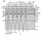
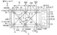
図1は、本発明の一実施形態に係る発光素子1の模式的な平面図である。図2は、図1の切断面線II−IIにおける断面図である。図3は、図1の切断面線III−IIIにおける断面図である。図4は、発光素子1の模式的な斜視図である。
発光素子1は、基板2と、第1導電型半導体層3と、発光層4と、第2導電型半導体層5と、透明電極層6と、反射電極層7と、絶縁層8と、絶縁管層9と、第1電極層10(n側電極)と、第1コンタクト11と、第2電極層12(p側電極)と、第2コンタクト13と、エッチングストップ層14と、バリア層15と、接合層16とを備えている。Hereinafter, embodiments of the present invention will be described in detail with reference to the accompanying drawings.
FIG. 1 is a schematic plan view of a
The
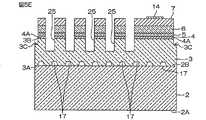
基板2上に、第1導電型半導体層3、発光層4、第2導電型半導体層5、透明電極層6、反射電極層7および絶縁層8が、この順番で積層されている。
基板2は、発光層4の発光波長(たとえば450nm)に対して透明な材料(たとえばサファイア、GaNまたはSiC)からなり、所定の厚さを有している。基板2は、その厚さ方向から見た平面視において、図2における左右方向に長手方向を有し、図2における奥行き方向に短手方向を有する矩形形状に形成されている(図1参照)。基板2の長手方向寸法は、たとえば、約1000μmであり、基板2の短手方向寸法は、たとえば、約500μmである。基板2では、図2における下面が表面2Aであり、図2における上面が裏面2Bである。表面2Aは、光が取り出される光取出し面である。裏面2Bは、基板2における第1導電型半導体層3との接合面である。基板2の裏面2Bには、第1導電型半導体層3側へ突出する凸部17が複数形成されている。複数の凸部17は、離散配置されている。具体的には、複数の凸部17は、基板2の裏面2Bにおいて、互いに間隔を空けて行列状に配置されていてもよいし、千鳥状に配置されていてもよい。各凸部17は、SiNで形成されていてもよい。On the
The
第1導電型半導体層3は、基板2上に積層されている。第1導電型半導体層3は、基板2の裏面2Bの全域を覆っている。第1導電型半導体層3は、この実施形態では、n型の半導体層であり、より具体的には、n型の窒化物半導体(たとえば、GaN)からなっていて、発光層4の発光波長に対して透明である。第1導電型半導体層3について、図2において基板2の裏面2Bを覆う下面を表面3Aといい、表面3Aとは反対側の上面を裏面3Bということにする。基板2の厚さ方向(第1導電型半導体層3の厚さ方向でもある)から見た平面視において、第1導電型半導体層3の裏面3Bの端部には、表面3A側へ凹んだ段付部分3Cが形成されている。 The first conductivity
発光層4は、第1導電型半導体層3上に積層されている。発光層4は、第1導電型半導体層3の裏面3Bにおいて段付部分3C以外の全域を覆っている。発光層4は、この実施形態では、Inを含む窒化物半導体(たとえばInGaN)からなり、その厚さは、たとえば、約100nmである。発光層4の発光波長は、たとえば440nm〜460nmである。 The
第2導電型半導体層5は、発光層4と同一パターンで発光層4上に積層されている。そのため、平面視において、第2導電型半導体層5の領域は、発光層4の領域と一致している。第2導電型半導体層5は、この実施形態ではp型の半導体層であり、より具体的にはp型の窒化物半導体(たとえば、GaN)からなっていて、発光層4の発光波長に対して透明である。このように、n型半導体層である第1導電型半導体層3とp型半導体層である第2導電型半導体層5とで発光層4を挟んだ発光ダイオード構造が形成されている。第2導電型半導体層5の厚さは、たとえば、約200nmである。この場合、第1導電型半導体層3、発光層4および第2導電型半導体層5の全体の厚さは、たとえば、約4.5μmである。 The second conductivity
透明電極層6は、第2導電型半導体層5と同一パターンで第2導電型半導体層5上に積層されている。透明電極層6は、ZnO(酸化亜鉛)またはITO(酸化インジウム錫)からなり、発光層4の発光波長に対して透明である。この実施形態では、透明電極層6は、ITOからなる。
反射電極層7は、透明電極層6と同一パターンで透明電極層6上に積層されている。反射電極層7は、銀と白金族金属と銅とを含む合金からなる。当該白金族金属として、白金やパラジウムを用いる事ができる。各金属の配合比率は、銀が98%程度であり、白金族金属および銅のそれぞれが1%程度である。このような合金からなる反射電極層7は、導電性が良好である。The
The
絶縁層8は、反射電極層7上に積層されている。平面視における絶縁層8の端部には、基板2側へ延びる延設部8Aが一体的に設けられている。延設部8Aは、絶縁層8の一部である。延設部8Aは、平面視における発光層4、第2導電型半導体層5、透明電極層6および反射電極層7のそれぞれの外側端面と、第1導電型半導体層3の段付部分3Cとを全域に亘って覆っている。発光層4の外側端面は、発光層4において第1導電型半導体層3および第2導電型半導体層5の間から露出した端面4Aである。絶縁層8および延設部8Aは、絶縁性材料(たとえば、SiN)で形成されている。 The insulating
絶縁管層9は、絶縁性材料(ここでは、絶縁層8と同じ材料)で形成されている。絶縁管層9は、絶縁層8から連続しており、基板2の厚さ方向に沿って基板2側へ延びる管状の層である。この実施形態では、絶縁管層9は、直線的な円管状であり、その外側の直径は、30μm以上50μm以下であり、その厚さは10μm〜20μm程度である。絶縁管層9は、反射電極層7、透明電極層6、第2導電型半導体層5および発光層4を貫通して、第1導電型半導体層3の厚さ途中まで到達している。 The insulating
絶縁管層9は、複数設けられており、複数の絶縁管層9は、平面視において離散して配置されている。具体的に、複数の絶縁管層9は、平面視において、均等に分散配置されている。
図1を参照して、複数の絶縁管層9は、基板2の主面に平行な第1方向Xに延びる第1配列ラインAと、第1方向Xに交差し、基板2の主面に平行な第2方向Yに延びる第2配列ラインBとのそれぞれに沿って配置されている。この実施形態では、絶縁管層9の数は、15であり、3行5列の行列状に配置されている。この場合、第1方向X(行方向)が基板2の短手方向に一致し、第2方向Y(列方向)が基板2の長手方向に一致していて、第1配列ラインA(第1方向X)と第2配列ラインB(第2方向Y)とが直交している。1本の第1配列ラインA上には、3つの絶縁管層9が等間隔で配列されていて、1本の第2配列ラインBには、5つの絶縁管層9が等間隔で配列されている。A plurality of insulating
Referring to FIG. 1, a plurality of insulating tube layers 9 intersects a first array line A extending in a first direction X parallel to the main surface of the
第1配列ラインAおよび第2配列ラインBは、円管状の絶縁管層9の円中心を通っている。そのため、一本の第1配列ラインA上において隣り合う絶縁管層9の間隔は、隣り合って平行に延びる第2配列ラインBの間隔Cである。また、一本の第2配列ラインB上において隣り合う絶縁管層9の間隔は、隣り合って平行に延びる第1配列ラインAの間隔Dである。 The first array line A and the second array line B pass through the circular center of the tubular insulating
基板2の主面に平行な平面内において、第1配列ラインAおよび第2配列ラインBの両方に対して傾斜して延びる第3配列ラインEを考える。第3配列ラインEは、隣り合う第1配列ラインA上にあり、かつ、隣り合う第2配列ラインB上にある絶縁管層9の円中心を通る。間隔C,Dが等しいとき、第3配列ラインEは、第1配列ラインAおよび第2配列ラインBの両方に対して45°で傾斜して延びていて、一本の第3配列ラインE上に複数の絶縁管層9が等しい間隔Fを隔てて並んでいる。このように、複数の絶縁管層9は、第1配列ラインA、第2配列ラインBおよび第3配列ラインEのそれぞれにおいて、一の絶縁管層9と、この絶縁管層9から最も近い絶縁管層9との間隔(間隔C、D、F)が一定になるように配列されている。この実施形態のように絶縁管層9が行列状に配置される場合には、間隔Fが間隔C,Dよりも大きい。間隔C,Dが等しい場合、一の絶縁管層9と、それに最も近い他の絶縁管層9との間隔は、間隔C,Dに等しい。この間隔C,D(最近接絶縁管層9間の距離)は、50μm以上150μm以下となるように設定されている。 Consider a third array line E extending in an inclined manner with respect to both the first array line A and the second array line B in a plane parallel to the main surface of the
第3配列ラインE上において隣接する一対の絶縁管層9の円中心を結ぶ線分を考えると、この線分の中点は、その周囲に存在する絶縁管層9から最も遠い地点(最遠点)である。このような最遠点と、それに最も近い絶縁管層9(この絶縁管層9内に配置される第1コンタクト11)との間の距離が150μm以下となるように、絶縁管層9の平面配置を設計することが好ましい。 Considering a line segment connecting the circle centers of a pair of adjacent insulating tube layers 9 on the third array line E, the midpoint of this line segment is the farthest point from the insulating
図2を参照して、第1電極層10は、絶縁層8上において図2における左側に偏った領域に積層されている。第1電極層10は、平面視において、図1および図2における左右方向(基板2の長手方向)において長手の矩形状に形成されており、平面視における絶縁層8の半分以上の領域を占めていて、当該領域における絶縁層8に接触している(図1参照)。第1電極層10は、導電性材料(たとえば、Al(アルミニウム)やAg(銀))からなる。第1電極層10の厚さは、100nm以上であり、好ましくは、約350nmである。図1を参照して、第1電極層10は、図1において左右方向に延びる1対の長手縁10Aと、1対の長手縁10Aと直交して延びる1対の短手縁10Bとを含んでいる。長手縁10Aおよび短手縁10Bは、平面視における第1電極層10の外形(輪郭)を規定する辺である。 Referring to FIG. 2, the
平面視において、複数の絶縁管層9のうち、1つの絶縁管層9は、矩形状の第1電極層10の重心位置Gに配置されていて、残りの絶縁管層9は、重心位置Gを基準(対称の中心)として点対称となるように配置されている。また、複数の絶縁管層9は、第1電極層10の長手縁10Aおよび短手縁10Bに沿って配置された第1縁側絶縁管層9Aを含んでいる。図1では、12個の第1縁側絶縁管層9Aが、全体で矩形の額縁状をなしていて、第1電極層10の外形線(長手縁10Aおよび短手縁10B)を縁取るように外形線に隣接して配置されている。 In plan view, one insulating
第1コンタクト11は、導電性材料(ここでは、第1電極層10と同じ材料)で形成されている。第1コンタクト11は、第1電極層10と同じ材料で形成されている場合、第1電極層10と一体化していてもよく、第1電極層10の一部と考えることもできる。第1コンタクト11は、第1電極層10から連続しており、基板2の厚さ方向に沿って基板2側へ延びる柱状に形成されている。この実施形態では、第1コンタクト11は、直線状の円柱形状である。第1コンタクト11は、複数設けられている。この実施形態では、第1コンタクト11は、絶縁管層9と同じ数(15個)だけ設けられている。各第1コンタクト11は、絶縁層8を貫通して、対応する絶縁管層9の中空部分に埋め込まれている。この状態で、各第1コンタクト11は、絶縁層8および絶縁管層9を通って、第1導電型半導体層3に接続されている。第1コンタクト11は、絶縁管層9を通ることによって、反射電極層7、透明電極層6、第2導電型半導体層5および発光層4から分離絶縁されている。第1導電型半導体層3に対する円柱形状の第1コンタクト11の接触部18は、円形状である。接触部18の直径は、たとえば20μm以上40μm以下であってもよく、第1コンタクト11の寸法誤差や隣り合う第1コンタクト11の間隔の誤差を踏まえると、好ましくは、30μm程度である。接触部18の直径を20μmよりも小さくすると、接触部18における電気抵抗(接触抵抗)が増大する。 The
全て(ここでは、15個)の第1コンタクト11の接触部18の面積(接触面積)の合計は、3000μm2以上25000μm2以下であることが好ましい。
図1を参照して、平面視において、円管状の絶縁管層9の円中心と、絶縁管層9の中空部分に埋め込まれた円柱状の第1コンタクト11の円中心とは、一致している。したがって、平面視において、複数の第1コンタクト11は、複数の絶縁管層9と同じ配列パターンで配列されている。つまり、複数の第1コンタクト11は、平面視において、第1配列ラインAおよび第2配列ラインBの交差点上に配置されていて、行列状をなすように、均等に分散配置されている。また、複数の第1コンタクト11は、第1配列ラインA、第2配列ラインBおよび第3配列ラインEの上において、一の第1コンタクト11と、この第1コンタクト11から最も近い第1コンタクト11との間隔が、それぞれ前述した間隔C、DおよびFで一定になるように配列されている。そして、複数の第1コンタクト11は、平面視において、第1電極層10の重心位置Gを基準として点対称となるように配置されている。複数の第1コンタクト11のうち、前述した第1縁側絶縁管層9Aの内側に埋め込まれた第1コンタクト11を、第1縁側コンタクト11Aということにする。この第1縁側コンタクト11Aは、平面視において、第1電極層10の長手縁10Aおよび短手縁10Bに沿って配置されている。All (here, 15) the sum of the areas of the
With reference to FIG. 1, in a plan view, the circle center of the tubular insulating
図2を参照して、第2電極層12は、この実施形態では、第1電極層10と同じ材料からなり、絶縁層8上において図2における右側に偏った領域に積層されている。第2電極層12は、平面視において、第1電極層10よりも小さいが、たとえば、第1電極層10と同じ厚さを有している。第2電極層12は、第1電極層10の長手方向(図1および図2における左右方向)に対して直交する方向(図2の紙面に直交する方向)に長手である(図1参照)。絶縁層8上において、左側に偏って形成された第1電極層10と、右側に偏って形成された第2電極層12とは、たとえば約60μmの距離を隔てることによって分離絶縁されている。 Referring to FIG. 2, in this embodiment, the
前述した第1縁側絶縁管層9Aにおいて、平面視において第1電極層10における第2電極層12側とは反対側の縁(図1における左側の短手縁10B)に沿って配置されている3つの第1縁側絶縁管層9Aを、第2縁側絶縁管層9Bということにする。そして、第1縁側絶縁管層9Aの内側に埋め込まれた第1縁側コンタクト11Aのうち、3つの第2縁側絶縁管層9Bの内側に埋め込まれた第1縁側コンタクト11Aを、第2縁側コンタクト11Bということにする。これらの第2縁側コンタクト11Bは、平面視において、当該左側の短手縁10Bに沿って配置されている。 In the first edge side insulating
第2コンタクト13は、導電性材料(ここでは、第2電極層12と同じ材料)で形成されている。第2コンタクト13は、第2電極層12から連続しており、基板2の厚さ方向に沿って基板2側へ延びる柱状に形成されている。第2コンタクト13は、複数(ここでは、3つ)設けられている。複数の第2コンタクト13は、第2電極層12の長手方向(図2の紙面に直交する方向)に沿って並んでいる(図1参照)。各第2コンタクト13は、絶縁層8を貫通している。 The
エッチングストップ層14は、反射電極層7上において、平面視で各第2コンタクト13と一致する位置に積層されており、平面視において第2コンタクト13よりも大きく形成されている。エッチングストップ層14は、導電性材料で形成されており、具体的には、Cr(クロム)およびPt(白金)を反射電極層7側からこの順番で積層することで構成されている。エッチングストップ層14は、反射電極層7と第2コンタクト13とに挟まれている。第2コンタクト13は、エッチングストップ層14を介して反射電極層7に接続されている。 The
バリア層15は、第1電極層10上に、第1電極層10と同一パターンで積層されているとともに、第2電極層12上に、第2電極層12と同一パターンで積層されている。バリア層15は、Ti(チタン)およびPtを第1電極層10および第2電極層12側からこの順番で積層して構成されている。
接合層16は、第1電極層10上のバリア層15上に、第1電極層10と同一パターンで積層されているとともに、第2電極層12上のバリア層15上に、第2電極層12と同一パターンで積層されている。接合層16は、たとえば、Ag、TiもしくはPtまたはこれらの合金からなる。接合層16は、半田またはAuSn(金錫)からなってもよい。この実施形態では、接合層16は、AuSnからなる。バリア層15によって、接合層16から第1電極層10および第2電極層12へのSn(錫)の拡散が抑えられている。The
The
接合層16において、第1電極層10上および第2電極層12上のバリア層15と接する面が下面であり、この下面とは反対側の上面を接合面16Aということにする。第1電極層10側の接合層16の接合面16Aと、第2電極層12側の接合層16の接合面16Aとはいずれも平坦面であり、同じ高さ位置(基板2の厚さ方向における位置)において面一になっている。前述したように第1電極層10と第2電極層12とが分離絶縁されているので、第1電極層10側の接合層16と、第2電極層12側の接合層16とは、分離絶縁されている。 In the
第1導電型半導体層3において段付部分3Cを除く部分と、発光層4と、第2導電型半導体層5と、透明電極層6と、反射電極層7とは、平面視において一致していて、図1および図2の左右方向(基板2の長手方向)に長手の矩形状である(図1参照)。第1導電型半導体層3、発光層4、第2導電型半導体層5、透明電極層6および反射電極層7のそれぞれは、絶縁管層9および第1コンタクト11が形成されていない領域では、基板2の長手方向における全域に亘って存在している(図3参照)。平面視において、第1電極層10、第2電極層12、バリア層15および接合層16は、発光層4(第2導電型半導体層5、透明電極層6、反射電極層7)の内側に位置している(図1参照)。 The portion of the first conductive
この発光素子1では、第1電極層10と第2電極層12との間に順方向電圧を印加すると、第2電極層12から第1電極層10へ向かって電流が流れる。電流は、第2電極層12から第1電極層10へ向かって、第2コンタクト13、エッチングストップ層14および反射電極層7を、この順番で流れる。反射電極層7は、導電性が良好なので、電流は、反射電極層7において平面視における全域に広がり、その後、透明電極層6、第2導電型半導体層5、発光層4、第1導電型半導体層3および第1コンタクト12を、この順番で流れる。このように電流が流れることによって、第1導電型半導体層3から発光層4に電子が注入され、第2導電型半導体層5から発光層4に正孔が注入され、これらの正孔および電子が発光層4で再結合することにより、波長440nm〜460nmの青色の光が発生する。この光は、第1導電型半導体層3および基板2をこの順で透過して基板2の表面2Aから取り出される。 In the
この際、発光層4から第2導電型半導体層5側に向かう光も存在し、この光は、第2導電型半導体層5および透明電極層6をこの順で透過して、透明電極層6と反射電極層7との界面で反射される。反射した光は、透明電極層6、第2導電型半導体層5、発光層4、第1導電型半導体層3および基板2をこの順で透過して基板2の表面2Aから取り出される。 At this time, there is also light traveling from the
また、反射電極層7で反射されずに、絶縁管層9内を進む光も存在し、この光は、絶縁管層9および絶縁層8を透過して、絶縁層8と第1電極層10および第2電極層12との界面で反射される。反射した光は、絶縁層8、絶縁管層9、透明電極層6、第2導電型半導体層5、発光層4、第1導電型半導体層3および基板2を透過して基板2の表面2Aから取り出される。つまり、この発光素子1は、第1の反射電極層としての反射電極層7のほかに、第2の反射電極層としての第1電極層10および第2電極層12を備えている。第1および第2電極層10,12が反射電極層としての機能を有すためには、第1および第2電極層10,12の厚さは、100nm以上である必要がある。 In addition, there is also light that travels through the insulating
前述したように、基板2の裏面2Bには、複数の凸部17が形成されている。これらの凸部17によって、第1導電型半導体層3側から基板2へ向かって様々な角度から基板2の裏面2Bに入射される光が基板2の裏面2Bで全反射することを抑制できる。これにより、第1導電型半導体層3から基板2へ向かう光が、第1導電型半導体層3と基板2との界面において第1導電型半導体層3側へ反射することが抑制される。すなわち、光の取り出し効率が向上する。 As described above, the plurality of
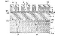
図5A〜図5Hは、図2に示す発光素子の製造方法を示す図解的な断面図である。
まず、図5Aに示すように、基板2の裏面2Bに、SiNからなる層(SiN層)を形成し、レジストパターン(図示せず)をマスクとするエッチングにより、このSiN層を、複数の凸部17に分離する。次いで、基板2を反応容器(図示せず)内に配置して反応容器内にガス(シランガス等)を流すことによって、基板2の裏面2B上に半導体層をエピタキシャル成長させる処理が行われる。その際、ガスの流量比を変えることで、基板2の裏面2B上に、第1導電型半導体層3、発光層4および第2導電型半導体層5を、この順番で連続的に形成することができる。5A to 5H are schematic cross-sectional views showing a method for manufacturing the light-emitting element shown in FIG.
First, as shown in FIG. 5A, a SiN layer (SiN layer) is formed on the
次いで、図5Bに示すように、たとえばリフトオフ法を用いて、透明電極層6をパターン形成する。透明電極層6は、各絶縁管層9(図1および図2参照)と一致する位置に、透明電極層6を貫通する貫通穴19を有するパターンに形成され。各貫通穴19から第2導電型半導体層5が露出することになる。
次いで、透明電極層6の上、および、第2導電型半導体層5において各貫通穴19からが露出された部分の上の全域に亘って、銀と白金族金属と銅とを含む合金の層(合金層)を形成し、この合金層に対して、図5Cに示すように、透明電極層6と同一パターンのレジストパターン20をマスクとするドライエッチングを施す。これにより、合金層が選択的に除去され、残った合金層が、反射電極層7となって、透明電極層6上に、透明電極層6と同一パターンで形成される。反射電極層7には、平面視で透明電極層6の各貫通穴19と一致する位置に、貫通穴19と同じ大きさの貫通穴21が形成されている。Next, as shown in FIG. 5B, the
Next, a layer of an alloy containing silver, a platinum group metal, and copper over the entire area of the
次いで、図5Dに示すように、レジストパターン20を除去してから、別のレジストパターン22を反射電極層7上に形成する。レジストパターン22には、平面視で反射電極層7の各貫通穴21と一致する位置に、貫通穴21と同じ大きさの開口23が形成されている。開口23は、平面視で同じ位置にある貫通穴19,21に連続している。また、平面視において、レジストパターン22は、第1導電型半導体層3の段付部分3Cが位置する予定の部分には存在しない。 Next, as shown in FIG. 5D, after removing the resist
次いで、レジストパターン22をマスクとするドライエッチングにより、反射電極層7、透明電極層6、第2導電型半導体層5、発光層4および第1導電型半導体層3のそれぞれを選択的に除去する。これにより、平面視においてレジストパターン22の各開口23と一致する位置には、第2導電型半導体層5および発光層4を貫通して、第1導電型半導体層3の厚さ途中まで到達するトレンチ24(この実施形態では円筒状のトレンチ)が形成され、第1導電型半導体層3に段付部分3Cが形成される。各トレンチ24は、平面視で同じ位置にある開口23および貫通穴19,21に連続している。平面視で同じ位置で連続する貫通穴19,21およびトレンチ24は、1つのトレンチ25を構成している。トレンチ25は、平面視で絶縁管層9と一致する複数(ここでは、15個)の分散した位置に形成されている。各トレンチ25は、この実施形態では、基板2の厚さ方向に直線的に延びる円筒状であり、その断面の円形状は、基板2の厚さ方向におけるいずれの位置でも同じ大きさである。各トレンチ25は、反射電極層7、透明電極層6、第2導電型半導体層5および発光層4を貫通して、第1導電型半導体層3の厚さ途中まで到達している。トレンチ25の半導体層表面(第2導電型半導体層5の表面)からの深さ(基板2の厚さ方向における寸法)は、たとえば、約1.5μmである。また、反射電極層7、透明電極層6、第2導電型半導体層5および発光層4のそれぞれにおいて平面視で段付部分3Cと一致する部分(図5C参照)は、ドライエッチングによるトレンチ25の形成と同時に除去されている。 Next, each of the
次いで、レジストパターン22を除去してから、図5Eに示すように、反射電極層7上において平面視で第2コンタクト13(図2参照)と一致する予定の位置に、たとえばリフトオフ法を用いて、エッチングストップ層14を形成する。
次いで、図5Fに示すように、反射電極層7上およびエッチングストップ層14上に、たとえばCVD法によって、SiNからなる層(SiN層)26を形成する。SiN層26は、各トレンチ25内に埋め尽くされるとともに、平面視における発光層4、第2導電型半導体層5、透明電極層6および反射電極層7のそれぞれの外側端面と、第1導電型半導体層3の段付部分3Cとを全域に亘って覆うように形成される。SiN層26において、反射電極層7上およびエッチングストップ層14上にある部分は、絶縁層8となり、平面視における発光層4、第2導電型半導体層5、透明電極層6および反射電極層7のそれぞれの外側端面と、第1導電型半導体層3の段付部分3Cとを覆っている部分は、延設部8Aとなる。また、SiN層26において、トレンチ25内に埋め込まれた部分は、絶縁管層9を形成することになる。Next, after removing the resist
Next, as shown in FIG. 5F, a layer (SiN layer) 26 made of SiN is formed on the
次いで、図5Gに示すように、絶縁層8上に、レジストパターン27を形成する。レジストパターン27には、平面視で各第1コンタクト11(図2参照)と一致する予定の位置に、開口28が形成されていて、平面視で各第2コンタクト13(図2参照)と一致する予定の位置に、開口29が形成されている。
次いで、レジストパターン27をマスクとするドライエッチングにより、絶縁層8と、各トレンチ25内のSiN層26とを選択的に除去する。これにより、平面視においてレジストパターン27の各開口28と一致する位置の絶縁層8およびSiN層26がレジストパターン27側から除去される。このドライエッチングの条件は、第1導電型半導体層3がエッチングされない条件になっている。そのため、各開口28におけるエッチングは、トレンチ25の底面における第1導電型半導体層3の手前でストップする。これにより、平面視においてレジストパターン22の各開口28と一致する位置には、絶縁層8およびSiN層26を貫通して第1導電型半導体層3まで到達するトレンチ30が形成される。Next, as shown in FIG. 5G, a resist
Next, the insulating
トレンチ30は、基板2の厚さ方向に延びる円筒状であり、その断面の円形状は、基板2の厚さ方向における全域に亘って同じ大きさである。トレンチ30は、第1コンタクト11と同じ数(ここでは、15個)形成されていて、各トレンチ30は、いずれかのトレンチ25の内側に配置されている。各トレンチ25が第1導電型半導体層3の厚さ途中まで到達しているので、各トレンチ30も、第1導電型半導体層3の厚さ途中まで到達している。各トレンチ30の底では、第1導電型半導体層3が露出されている。各トレンチ25内に埋め尽くされたSiN層26は、トレンチ30が形成されることによって、絶縁管層9となる。 The
ここでのドライエッチングによって、平面視においてレジストパターン27の各開口29と一致する位置の絶縁層8がレジストパターン27側から除去される。各開口29におけるエッチングは、エッチングストップ層14で停止する。つまり、エッチングストップ層14が、その直下にある反射電極層7をドライエッチングから保護するので、反射電極層7までエッチングされてしまうことを防止できる。その結果、平面視においてレジストパターン27の各開口29と一致する位置には、絶縁層8を貫通してエッチングストップ層14まで到達するトレンチ31が形成される。トレンチ31は、第2コンタクト13と同じ数(ここでは、3個)だけ形成され、これらのトレンチ31は、平面視における基板2の短手方向(図5Gの紙面に直交する方向)において等間隔で並んでいる。 By this dry etching, the insulating
次いで、レジストパターン27を除去してから、図5Hに示すように、たとえば蒸着により、Alからなる層(Al層32)を絶縁層8上の全域に形成する。Al層32は、各トレンチ30内および各トレンチ31内に埋め尽くされる。トレンチ30内のAl層32は、第1コンタクト11となり、トレンチ31内のAl層32は、第2コンタクト13となる。 Next, after removing the resist
次いで、絶縁層8上のAl層32上の全域に、たとえばスパッタ法によって、Tiからなる層(Ti層)と、Ptからなる層(Pt層)とをAl層32側からこの順番で積層する。これにより、Ti層およびPt層の積層構造からなるバリア層15がAl層32上に形成される。
次いで、バリア層15上の全域に、たとえば電解めっき法によって、AuSnからなる層(AuSn層)を形成する。AuSn層は、接合層16である。Next, a layer made of Ti (Ti layer) and a layer made of Pt (Pt layer) are laminated in this order from the
Next, a layer made of AuSn (AuSn layer) is formed over the entire area of the
次いで、レジストパターン(図示せず)をマスクとして用いるエッチングにより、絶縁層8上のAl層32、バリア層15および接合層16のそれぞれを、平面視における基板2の長手方向において、第2コンタクト13と、第2コンタクト13に最も近い第1コンタクト11との間で二分する(図5H参照)。これにより、図2に示すように、絶縁層8上のAl層32において、平面視で全ての第1コンタクト11を覆う部分が、第1電極層10となり、平面視で全ての第2コンタクト13を覆う部分が、第2電極層12となる。この結果、発光素子1が完成する。第1電極層10および第2電極層12は、分離絶縁された状態で絶縁層8上に形成されている。 Next, by etching using a resist pattern (not shown) as a mask, each of the
発光素子1は、たとえば、元基板としての1枚のウエハ(図示せず)上に多数同時に形成される。そこで、必要に応じてウエハを研削・研磨して厚みを調整した後に、ウエハをダイシングすると、最終的に図1〜図4に示す構造の発光素子1が個別に切り出される。
第1コンタクト11が埋め込まれるトレンチ30は、第1コンタクト11と同じ大きさの円形状の断面を有しており、その直径(内径)は、20μm以上40μm以下である。これに対し、第2コンタクト13が埋め込まれるトレンチ31は、平面視においてトレンチ30よりも大きい(図1参照)。そのため、前述したように、絶縁層8上にAl層32を形成する際に(図5H参照)、各トレンチ31内にAl層32を埋め尽くすと、絶縁層8には、各トレンチ31の跡90が凹みとなって現れ、最終的には、第2電極12上の接合層16の接合面16Aにも現れる(図4参照)。しかし、複数のトレンチ31は、基板2の短手方向において間隔を隔てているので(図1参照)、これらのトレンチ31が1列につながっている場合に比べて、各トレンチ31の跡90は、とても小さく目立たない。そのため、第2電極12上の接合層16の接合面16Aはほとんど平坦になる。For example, a large number of
The
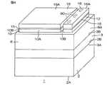
図6は、サブマウントの構造を図解的に示す断面図である。
図6に二点鎖線で示すように、発光素子1は、接合層16によってサブマウント50に接合され、発光素子ユニット64を構成する。
サブマウント50は、ベース基板51と、絶縁層52と、電極層53と、接合層54とを備えている。FIG. 6 is a cross-sectional view schematically showing the structure of the submount.
As shown by a two-dot chain line in FIG. 6, the
The
ベース基板51はたとえばSiからなる。絶縁層52は、たとえばSiO2からなり、ベース基板51の表面(図6における上面)の全域を覆っている。
電極層53は、たとえばAlからなる。電極層53は、絶縁層52上において分離された2つの領域に設けられており、図6では、2つの電極層53が、左右に隔てた状態で絶縁層52上に形成されている。2つの電極層53のうち、図6における左側の電極層53を第1マウント電極層53Aといい、図6における右側の電極層53を第2マウント電極層53Bということにする。第1マウント電極層53Aと第2マウント電極層53Bとは、第1電極11および第2電極12の間隔とほぼ等しい間隔、たとえば、60μm程度の間隔を隔てて分離絶縁されて配置されている。The
The
接合層54は各電極層53上に積層されている。接合層54は、この実施形態では、ベース基板51側のTi層55と、Ti層55上に積層されたAu層56とを含む2層構造である。接合層54において電極層53に接触している面とは反対側の面(図6における上面)が、表面54Aとされる。表面54Aは、平坦面であり、各電極層53上の接合層54の表面54Aは、面一になっている。 The
図7は、サブマウントの模式的な平面図である。
平面視において、第1マウント電極層53A上の接合層54は、発光素子1の第1電極層10上の接合層16と同じ大きさであり、第2マウント電極層53B上の接合層54は、発光素子1の第2電極層12上の接合層16と同じ大きさである(図1参照)。
図8Aは、発光装置の構造を図解的に示す断面図である。FIG. 7 is a schematic plan view of the submount.
In plan view, the
FIG. 8A is a cross-sectional view schematically showing the structure of the light-emitting device.
図8Aを参照して、発光装置60は、発光素子1と、サブマウント50と、支持基板61とを含んでいる。
支持基板61は、絶縁性材料で形成された絶縁基板62と、絶縁基板62の両端から露出するように設けられて、発光素子1と外部とを電気的に接続する金属製の一対のリード63とを有している。絶縁基板62は、たとえば平面視矩形に形成されており、その対向する一対の辺に沿って一対のリード63がそれぞれ帯状に形成されている。各リード63は、絶縁基板62の一対の端縁に沿って、上面から側面を渡って下面に至るように折り返され、横向きU字形断面を有するように形成されている。With reference to FIG. 8A, the
The
組立に際しては、たとえば、サブマウント50を、図8Aに示すように、接合層54の表面54Aが上を向くような姿勢にする。また、図2に示す発光素子1を、接合層16の接合面16Aが下を向くような姿勢(図2とは上下が逆の姿勢)にし、図8Aの姿勢にあるサブマウント50に対して上から対向させる。
発光素子1をサブマウント50に接近させると、図8Aに示すように、発光素子1の接合層16の接合面16Aと、サブマウント50の接合層54の表面54Aとが面接触する。具体的には、第1電極層10側の接合層16の接合面16Aが、第1マウント電極層53A側の接合層54の表面54Aに対して面接触し、第2電極層12側の接合層16の接合面16Aが、第2マウント電極層53B側の接合層54の表面54Aに対して面接触する。この状態でリフロー(熱処理)を行えば、第1電極層10と第1マウント電極層53Aとが接合層16,54を介して接合され、かつ第2電極層12と第2マウント電極層53Bとが接合層16,54を介して接合されて、発光素子1がサブマウント50にフリップチップ接続される。すなわち、接合層16と接合層54とが融解・固着して互いに接合する。その結果、発光素子1とサブマウント50とが一体化した発光素子ユニット64が得られる。At the time of assembly, for example, the
When the
前述したように、第2電極12上の接合層16の接合面16Aには、各トレンチ31の跡90があるがとても小さいので、この接合面16Aは、ほとんど平坦である(図4参照)。そのため、この接合面16Aと、第2マウント電極層53B側の接合層54の表面54Aとの面接触に対して、各トレンチ31の跡90が影響を与えることはなく、これらの接合面16Aおよび表面54Aは、ほぼ全域に亘って面接触している。また、発光素子1側の第1電極層10と第2電極層12とが、約60μmという十分な距離を隔てていて、サブマウント50側の第1マウント電極層53Aと第2マウント電極層53Bとが、同様に十分な距離を隔てている。そのため、多少の取り付け誤差があっても、第1電極層10が第2マウント電極層53Bに接続されたり、第2電極層12が第1マウント電極層53Aに接続されたりすることがないので、発光素子1をサブマウント50に確実にフリップチップ接続できる。 As described above, the
発光素子ユニット64は、サブマウント50のベース基板51を絶縁基板62の一表面に対向させて、当該絶縁基板62に接合される。そして、第1電極層10に接続された第1マウント電極層53Aと、第1マウント電極層53A側のリード63とが、ボンディングワイヤ65によって接続される。また、第2電極層12に接続された第2マウント電極層53Bと、第2マウント電極層53B側のリード63とが、ボンディングワイヤ65によって接続される。これにより、発光素子ユニット64と支持基板61とが一体化されて発光装置60が完成する。 The light emitting
図8Bに図解的な斜視図を示すように、支持基板61は、長尺形状(帯状)に形成されていてもよく、このような長尺な支持基板61の表面に、複数の発光素子ユニット64が実装されてLED(発光ダイオード)バーを構成していてもよい。図8Bには、支持基板61の一表面に複数の発光素子ユニット64が直線状に一列に配列された発光装置60が示されている。このような発光装置60は、たとえば、液晶表示装置のバックライト用光源として用いることができる。なお、支持基板61上の複数の発光素子ユニット64は、直線状に一列に配列されている必要はなく、2列に配列されていてもよいし、千鳥状に配列されていてもよい。また、各発光素子ユニット64上に、蛍光体を含んだ封止樹脂をポッティングしてもよい。 As shown in the schematic perspective view of FIG. 8B, the
図9は、発光素子ユニット64を用いた発光素子パッケージの模式的な斜視図である。
発光素子パッケージ70は、図8Aに示した構造の発光装置60と樹脂パッケージ71と封止樹脂72とを含んでいる。
樹脂パッケージ71は、樹脂が充填されたリング状のケースであり、その内側に発光素子ユニット64を収容して(覆って)側方から包囲して保護した状態で、支持基板61に固定されている。樹脂パッケージ71の内壁面は、発光素子ユニット64の発光素子1から出射された光を反射させて外部へ取り出すための反射面71aを形成している。この実施形態では、反射面71aは、内方に向かうに従って支持基板61に近づくように傾斜した傾斜面からなり、発光素子1からの光を光取り出し方向(基板2の法線方向)に向かって反射するように構成されている。FIG. 9 is a schematic perspective view of a light emitting device package using the light emitting
The light emitting
The
封止樹脂72は、発光素子1の発光波長に対して透明な透明樹脂(たとえば、シリコーンやエポキシなど)からなり、発光素子1およびボンディングワイヤ65などを封止している。または、この透明樹脂に蛍光体を混合してもよい。発光装置60が青色発光し、蛍光体として黄色発光のものを配置すると、自然発光が得られる。
図9には、支持基板61上に一つの発光素子ユニット64が実装されている構造を示したが、むろん、支持基板61上に複数個の発光素子ユニット64が共通に実装されていて、それらが封止樹脂72によって共通に封止されていてもよい。The sealing
FIG. 9 shows a structure in which one light emitting
図10は、発光ダイオードにおける電流密度と光出力との関係を示すグラフである。
図10を参照して、発光ダイオードでは、理論上は、電流密度が高くなると、光出力が線形に増加すると期待される(図10の破線の理論ライン)。しかし、実際には、電流密度が高くなると、いわゆるドループ現象が発生することで光出力のロスが生じるので、光出力は、理論ラインから下方(低下する側)へずれた特性線(図10の実線)に沿う。FIG. 10 is a graph showing the relationship between current density and light output in a light emitting diode.
Referring to FIG. 10, in the light-emitting diode, it is theoretically expected that the light output increases linearly as the current density increases (theoretical line indicated by the broken line in FIG. 10). However, in reality, when the current density is increased, a so-called droop phenomenon occurs, resulting in a loss of optical output. Therefore, the optical output is shifted from the theoretical line to the downward (lowering side) characteristic line (see FIG. 10). Along the solid line).
発光素子1に印加する電流を一定として発光効率を向上させるためには、光出力のロスを減らす必要があり、そのためには、電流密度を緩和する(下げる)必要がある。電流密度を緩和するためには、図1に示す平面視において発光層4を大きくすることが有効だが、そのために基板2(チップ全体)を大きくするのでは、コスト上昇が避けられない。そこで、基板2の大きさ(チップサイズ)を変えずに、平面視において、発光層4を大きくして、基板2において発光層4が占める割合(実発光面積比という)を大きくすることが望ましく、そのために、この発明の一実施形態に係る発光素子1は、以上に述べた構成を有している。 In order to improve the light emission efficiency while keeping the current applied to the
つまり、図2に示したとおり、発光素子1では、第1電極層10と第1導電型半導体層3とは、これらの間に発光層4、第2導電型半導体層5、透明電極層6、反射電極層7および絶縁層8を挟むことによって、離れて配置されている。そして、第1電極層10は、平面視において離散配置された複数の第1コンタクト11を介して第1導電型半導体層3に接続されている。そのため、第1電極層10が第1導電型半導体層3上に直接積層された場合と同程度に、第1電極層10と第1導電型半導体層3との間で電流を円滑に流すことができる。 That is, as shown in FIG. 2, in the
第1電極層10が第1導電型半導体層3上に直接積層されている場合における第1電極層10と第1導電型半導体層3との接触部の面積に比べて、離散配置された複数の第1コンタクト11と第1導電型半導体層3との接触部18の総面積は、小さく抑えることができる。これは、第1コンタクト11が離散配置されていることによって、第1導電型半導体層3の全体に十分に電流を分散させることができるからである。これにより、発光層4が、第1電極層10と第1導電型半導体層3とを接続するための構成によって浸食されることを抑えることができる。そのため、発光素子1では、第1導電型半導体層3上の発光層4の面積を大きくすることができるので、電流密度を抑制でき、それに応じて、発光効率の向上を図ることができる。 Compared with the area of the contact portion between the
前述のとおり、本願発明者は、特許文献1に記載された構造を発展させて、端部領域および端部領域から延びる複数の枝部を有する露出したn型半導体層と、その上に配置したn電極(n型半導体層と同様に複数の枝部を有する)の構造(比較例)を検討した。この比較例における、電流密度と発光効率との関係を、図11に破線で示。すなわち、この比較例の構造では、n電極の枝部を配置するために、発光層が大きく浸食されるため、発光層の面積が小さくなり、その結果、発光効率が悪くなる。 As described above, the inventor of the present application developed the structure described in
そこで、本願発明者は更に研究を進め、複数の第1コンタクト11を有するこの実施形態の発光素子1の構造に想到し、この構造を適用することによって、発光層4の面積を大きくしつつ、発光層4全体を均一に光らせることに成功した。この実施形態の構造に対応する実施例について電流密度と発光効率との関係を調べた結果を、図11に実線で示す。この図11の2つの曲線の比較から、電流密度の全領域において発光効率が向上していることが分かる。また、第1電極層10を第1導電型半導体層3上に直接積層せずに、絶縁層8上に積層しているので、第1電極層10を、第1導電型半導体層3上の発光層4に影響されることなく、大きくすることができた。 Therefore, the inventor of the present application has further researched and conceived the structure of the
また、この実施形態の構造では、複数の第1コンタクト11は、平面視において、均等に分散配置されている(図1参照)。そのため、第1電極層10への電流の取り込み部分(接触部18)が第1導電型半導体層3において広い範囲で均等に分布しているので、電流が発光層4内の広い範囲に均等に行き渡る。これにより、発光層4において光る部分を一層増やすことができるので、発光素子1の発光効率の更なる向上を図ることができる。また、広い範囲で均等に分布した取り込み部分を介して、第1導電型半導体層3から第1電極層10側へ円滑に電流を流すことができる。 In the structure of this embodiment, the plurality of
また、図1を参照して、複数の第1コンタクト11を平面視において均等に分散配置するために、複数の第1コンタクト11は、一の第1コンタクト11と、この第1コンタクト11から最も近い第1コンタクト11との間隔(前述した間隔C、D)が一定になるように配置されている。
複数の第1コンタクト11は、平面視において第1電極層10の縁(長手縁10Aおよび短手縁10B)に沿って配置された第1縁側コンタクト11Aを含んでいるので、第1縁側コンタクト11Aに応じて、第1導電型半導体層3では、少なくとも縁側に、前記取り込み部分(図2の接触部18)が配置される。これにより、第1導電型半導体層3上の発光層4内では、縁側まで電流を行き渡らせることができる。そのため、発光層4において光る部分を増やすことができるので、発光素子1の発光効率の向上を図ることができる。In addition, referring to FIG. 1, in order to evenly distribute the plurality of
Since the plurality of
複数の第1コンタクト11は、平面視において第1電極層10における第2電極層12側とは反対側の縁(図1における左側の短手縁10B)に沿って配置された第2縁側コンタクト11Bを含んでいるので、第2縁側コンタクト11Bに応じて、第1導電型半導体層3では、少なくとも第2電極層12側とは反対の縁側に、前記取り込み部分が配置される。これにより、第1導電型半導体層3上の発光層4内では、第2電極層12側とは反対の縁側まで電流を行き渡らせることができる。そのため、発光層4において光る部分を増やすことができるので、発光素子1の発光効率の向上を図ることができる。 The plurality of
第1導電型半導体層3に対する第1コンタクト11の接触部18は、円形状であるので、この接触部18、つまり、前記取り込み部分では、その円形状の全周に亘って電流を取り込むことができる。これにより、第1導電型半導体層3から第1コンタクト11へ円滑に電流を流すことができる。
第1導電型半導体層3に対する全ての第1コンタクト11の接触部18の面積の合計(第1コンタクト総面積)は、3000μm2以上25000μm2以下である。Since the
Sum of the areas of the
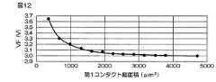
図12は、第1コンタクト総面積と順方向電圧(VF)との関係を示すグラフである。図12に示すように、第1コンタクト総面積が増加するのに従って、発光素子1における順方向電圧(VF)が低下し、第1コンタクト総面積が3000μm2以上であると、順方向電圧がほぼ一定になる。すなわち、第1コンタクト総面積を大きくすると、接触部18における抵抗が小さくなって電流が流れ易くなるが、第1コンタクト総面積が3000μm2以上の範囲では、順方向電圧VFは飽和傾向となることが分かる。FIG. 12 is a graph showing the relationship between the first contact total area and the forward voltage (VF). As shown in FIG. 12, as the first contact total area increases, the forward voltage (VF) in the light-emitting
図13は、第1コンタクト総面積と発光効率との関係を示すグラフである。図13に示すように、第1コンタクト総面積が増加するのに従って、発光素子1の発光効率が向上し、第1コンタクト総面積が3000μm2以上であると、発光効率は最大値でほぼ一定になる。一方、第1コンタクト総面積が25000μm2を超えると、発光層4の面積が小さく(狭く)なることによる影響が大きくなり、発光効率は低下する。FIG. 13 is a graph showing the relationship between the first contact total area and the light emission efficiency. As shown in FIG. 13, as the total first contact area increases, the light emission efficiency of the light-emitting
このように、発光素子1では、第1コンタクト総面積を3000μm2以上25000μm2以下とすることで、順方向電圧VFを低下させつつ、発光効率の向上を図ることができる。
図2を参照して、第1電極層10は、絶縁層8に接するとともに第1コンタクト11を有し、絶縁層8を透過した光を反射させる第2の反射電極層を構成している。そのため、透明電極層6上に積層された反射電極層7で反射せず絶縁層8を透過した光を第1電極層10で反射させることにより、光の反射効率を向上させることができ、その分、発光素子1の発光効率の向上を図ることができる。Thus, the
Referring to FIG. 2, the
絶縁層8は、発光層4において第1導電型半導体層3および第2導電型半導体層5の間から露出した端面4Aを覆っているので、発光層4が発光したときに、光が発光層4の端面4Aから漏れることを防止できる。これにより、発光素子1の発光効率の向上を図ることができる。
本発明の実施形態に係る発光素子1では、発光層4を大きくする(平面視で広くする)ことによって、前述した実発光面積比が、たとえば約79%となる。特許文献1の構造を改良した前述の比較例に係る発光素子では、たとえば実発光面積比が約63%である。したがって、この比較例に対して、実発光面積比を約16%向上できた。これにより、図11の実線(実施例)に示すように、電流密度の全域において、発光効率が1%程度向上した。前述した比較例に係る発光素子に約100mAを印加したときの電流密度は、たとえば、300mA/mm2であって、発光効率は約28%である(図11のポイントA)。一方、この実施形態を適用した実施例に係る発光素子1では、たとえば、同じ電流を印加したときの電流密度が約200mA/mm2まで緩和され、図11のポイントBに示すように、発光効率が約31%まで上昇した。Since the insulating
In the
図14は、第1の変形例に係る発光素子の模式的な平面図である。図15は、第2の変形例に係る発光素子の模式的な平面図である。
図14に示すように、第1コンタクト11は、平面視において、第1電極層10の長手縁10Aに沿って配置された第1縁側コンタクト11Aだけをふくんでいてもよい。
また、図15に示すように、第1コンタクト11は、平面視において、千鳥状に配置されていてもよい。この場合、第1電極層10の長手縁10A沿いの第1縁側コンタクト11Aは、前述した第2配列ラインB上に並んで配置されていて、それ以外の第1コンタクト11は、前述した第3配列ラインE上に並んで配置されている。FIG. 14 is a schematic plan view of a light emitting device according to a first modification. FIG. 15 is a schematic plan view of a light emitting device according to a second modification.
As shown in FIG. 14, the
Further, as shown in FIG. 15, the
図14および図15のいずれの場合においても、第1コンタクト11は、第1電極層10の重心位置Gを基準(対称の中心)として点対称となるように配置されている。
ただし、以上で説明した以外にも、第1コンタクト11の配置は、適宜変更可能であり、たとえば、重心位置Gを基準(対称の中心)として点対称となるように配置されていなくてもよい。この場合には、発光層4において電流を広く行き渡らせるために、第1電極層10において第2電極12から遠い側の短手縁10Bに沿う第2縁側コンタクト11Bを少なくとも配置することが好ましい。14 and 15, the
However, besides the above description, the arrangement of the
以上のほかにも、この発明はさらに種々の実施形態をとり得る。たとえば、前述の実施形態では、第1コンタクト11が円柱形状を有する例を示したが、第1コンタクト11は多角柱形状を有していてもよい。また、第1コンタクト11は、その軸直角断面形状が軸方向に沿って一様である必要はなく、たとえば、接触部18から離れるに従って断面積が大きくなるように設計されていてもよい。また、前述の実施形態では、第1導電型がn型で、第2導電型がp型の例について説明したが、第1導電型をp型とし、第2導電型をn型として発光素子を構成してもよい。すなわち、前述の実施形態において、導電型をp型とn型とで反転した構造も、この発明の一つの実施形態である。また、前述の実施形態では、窒化物半導体としてGaNを例示したが、窒化アルミニウム(AlN)、窒化インジウム(InN)などの他の窒化物半導体が用いられてもよい。窒化物半導体は、一般には、AlxInyGa1-x-yN(0≦x≦1,0≦y≦1,0≦x+y≦1)と表わすことができる。また、窒化物半導体に限らず、GaAs等の他の化合物半導体や、化合物半導体以外の半導体材料(たとえばダイヤモンド)を用いた発光素子にこの発明を適用してもよい。In addition to the above, the present invention can take various embodiments. For example, in the above-described embodiment, the example in which the
1 発光素子
2 基板
3 第1導電型半導体層
4 発光層
4A 端面
5 第2導電型半導体層
6 透明電極層
7 反射電極層
8 絶縁層
9 絶縁管層
10 第1電極層
10A 長手縁
10B 短手縁
11 第1コンタクト
11A 第1縁側コンタクト
11B 第2縁側コンタクト
12 第2電極層
13 第2コンタクト
14 エッチングストップ層
16 接合層
18 接触部
50 サブマウント
64 発光素子ユニット
70 発光素子パッケージ
71 樹脂パッケージ
C 間隔
D 間隔
F 間隔
G 重心位置DESCRIPTION OF
Claims (26)
Translated fromJapanese前記第1導電型半導体層上に積層された発光層と、
前記発光層上に積層された第2導電型半導体層と、
前記第2導電型半導体層上に積層され、前記発光層の発光波長に対して透明な透明電極層と、
前記透明電極層上に積層され、前記透明電極層を透過した光を反射させる反射電極層と、
前記反射電極層上に積層された絶縁層と、
前記絶縁層上に積層された第1電極層と、
前記第1電極層から分離絶縁された状態で前記絶縁層上に積層された第2電極層と、
前記第1導電型半導体層の厚さ方向から見た平面視において離散して配置されており、前記絶縁層から連続して前記反射電極層、透明電極層、第2導電型半導体層および発光層を貫通し、前記第1導電型半導体層に到達する複数の絶縁管層と、
前記第1電極層から連続し、前記絶縁層および前記絶縁管層を通って前記第1導電型半導体層に接続された第1コンタクトと、
前記第2電極層から連続し、前記絶縁層を貫通して前記反射電極層に接続された第2コンタクトとを含み、
前記平面視において、前記発光層、前記第2導電型半導体層、前記透明電極層および前記反射電極層のそれぞれの領域が一致していて、
前記絶縁層は、前記反射電極層において前記平面視で前記絶縁管層と前記第2コンタクトによる開口部とを除く全てを覆うように前記反射電極層上に積層されている、発光素子。A first conductivity type semiconductor layer;
A light emitting layer laminated on the first conductivity type semiconductor layer;
A second conductivity type semiconductor layer stacked on the light emitting layer;
A transparent electrode layer laminated on the second conductivity type semiconductor layer and transparent to the emission wavelength of the light emitting layer;
A reflective electrode layer that is laminated on the transparent electrode layer and reflects light transmitted through the transparent electrode layer; and
An insulating layer laminated on the reflective electrode layer;
A first electrode layer laminated on the insulating layer;
A second electrode layer laminated on the insulating layer in a state of being separated and insulated from the first electrode layer;
The reflective electrode layer, the transparent electrode layer, the second conductive semiconductor layer, and the light emitting layer are arranged discretely in a plan view as viewed from the thickness direction of the first conductive semiconductor layer, and continuously from the insulating layer. A plurality of insulating tube layers that pass through the first conductive type semiconductor layer,
A first contact continuous from the first electrode layer and connected to the first conductive semiconductor layer through the insulating layer and the insulating tube layer;
A second contact that is continuous from the second electrode layer and penetrates the insulating layer and is connected to the reflective electrode layer ;
PriorKitaira plane view, the light emitting layer, the second conductive semiconductor layer, each region of the transparent electrode layer and the reflective electrode layeris match,
The insulating layer thatis stacked on the reflective electrode layer the plan view in the insulating tube layer and the second contact by the opening and the reflective electrode layer so as to cover all but the light emittingelement.
前記絶縁層に接するとともに前記第1コンタクトを有し、前記絶縁層を透過した光を反射させる第2の反射電極層を含む、請求項1〜16のいずれか一項に記載の発光素子。The first electrode layer includes
The light emitting element according to any one of claims1 to16 , further comprising a second reflective electrode layer that is in contact with the insulating layer and has the first contact and reflects light transmitted through the insulating layer.
前記接合層に接合されたサブマウントとを含む、発光素子ユニット。A light emitting device according to claim2 3 or2 4,
A light-emitting element unit including a submount bonded to the bonding layer.
Priority Applications (1)
| Application Number | Priority Date | Filing Date | Title |
|---|---|---|---|
| JP2015115124AJP6009041B2 (en) | 2015-06-05 | 2015-06-05 | Light emitting device, light emitting device unit, and light emitting device package |
Applications Claiming Priority (1)
| Application Number | Priority Date | Filing Date | Title |
|---|---|---|---|
| JP2015115124AJP6009041B2 (en) | 2015-06-05 | 2015-06-05 | Light emitting device, light emitting device unit, and light emitting device package |
Related Parent Applications (1)
| Application Number | Title | Priority Date | Filing Date |
|---|---|---|---|
| JP2010290551ADivisionJP5777879B2 (en) | 2010-12-27 | 2010-12-27 | Light emitting device, light emitting device unit, and light emitting device package |
Publications (2)
| Publication Number | Publication Date |
|---|---|
| JP2015173294A JP2015173294A (en) | 2015-10-01 |
| JP6009041B2true JP6009041B2 (en) | 2016-10-19 |
Family
ID=54260395
Family Applications (1)
| Application Number | Title | Priority Date | Filing Date |
|---|---|---|---|
| JP2015115124AActiveJP6009041B2 (en) | 2015-06-05 | 2015-06-05 | Light emitting device, light emitting device unit, and light emitting device package |
Country Status (1)
| Country | Link |
|---|---|
| JP (1) | JP6009041B2 (en) |
Families Citing this family (5)
| Publication number | Priority date | Publication date | Assignee | Title |
|---|---|---|---|---|
| TWI559056B (en)* | 2015-12-11 | 2016-11-21 | 友達光電股份有限公司 | Light source module |
| US10263150B2 (en) | 2016-05-10 | 2019-04-16 | Rohm Co., Ltd. | Semiconductor light emitting device capable of increasing luminous efficiency under a low applied current |
| WO2018016894A1 (en)* | 2016-07-20 | 2018-01-25 | 엘지이노텍 주식회사 | Semiconductor device |
| KR102490507B1 (en)* | 2022-09-29 | 2023-01-19 | 주식회사 루미디아 | Transparent glass display substrate manufacturiing method and transparent glass display substrate manufactured therefrom |
| KR102497890B1 (en)* | 2022-09-29 | 2023-02-09 | 주식회사 루미디아 | Transparent glass display substrate manufacturiing method and transparent glass display substrate manufactured therefrom |
Family Cites Families (17)
| Publication number | Priority date | Publication date | Assignee | Title |
|---|---|---|---|---|
| KR100568269B1 (en)* | 2003-06-23 | 2006-04-05 | 삼성전기주식회사 | Gallium nitride based light emitting diode for flip-chip bonding and manufacturing method thereof |
| TWI220578B (en)* | 2003-09-16 | 2004-08-21 | Opto Tech Corp | Light-emitting device capable of increasing light-emitting active region |
| WO2005050748A1 (en)* | 2003-11-19 | 2005-06-02 | Nichia Corporation | Semiconductor device and method for manufacturing same |
| US7274040B2 (en)* | 2004-10-06 | 2007-09-25 | Philips Lumileds Lighting Company, Llc | Contact and omnidirectional reflective mirror for flip chipped light emitting devices |
| JP2006140234A (en)* | 2004-11-10 | 2006-06-01 | Sony Corp | Semiconductor light emitting element and its manufacturing method |
| TWI292631B (en)* | 2005-02-05 | 2008-01-11 | Epistar Corp | Light emitting diode and method of the same |
| KR100638813B1 (en)* | 2005-04-15 | 2006-10-27 | 삼성전기주식회사 | Flip chip type nitride semiconductor light emitting device |
| US20070045638A1 (en)* | 2005-08-24 | 2007-03-01 | Lumileds Lighting U.S., Llc | III-nitride light emitting device with double heterostructure light emitting region |
| JP2007243074A (en)* | 2006-03-10 | 2007-09-20 | Mitsubishi Cable Ind Ltd | Group iii nitride light emitting diode |
| JP4353232B2 (en)* | 2006-10-24 | 2009-10-28 | ソニー株式会社 | Light emitting element |
| JP2008117902A (en)* | 2006-11-02 | 2008-05-22 | Sumitomo Electric Ind Ltd | Method of manufacturing nitride semiconductor device |
| JP5032138B2 (en)* | 2007-01-26 | 2012-09-26 | 株式会社アルバック | Method for manufacturing light-emitting diode element |
| JP2008192782A (en)* | 2007-02-05 | 2008-08-21 | Toyota Central R&D Labs Inc | Electrode and Group III nitride compound semiconductor light emitting device having the same |
| US8368100B2 (en)* | 2007-11-14 | 2013-02-05 | Cree, Inc. | Semiconductor light emitting diodes having reflective structures and methods of fabricating same |
| JP5057398B2 (en)* | 2008-08-05 | 2012-10-24 | シャープ株式会社 | Nitride semiconductor light emitting device and manufacturing method thereof |
| JP5311408B2 (en)* | 2008-12-26 | 2013-10-09 | シャープ株式会社 | Nitride semiconductor light emitting device |
| JP5021693B2 (en)* | 2009-04-14 | 2012-09-12 | スタンレー電気株式会社 | Semiconductor light emitting device |
- 2015
- 2015-06-05JPJP2015115124Apatent/JP6009041B2/enactiveActive
Also Published As
| Publication number | Publication date |
|---|---|
| JP2015173294A (en) | 2015-10-01 |
Similar Documents
| Publication | Publication Date | Title |
|---|---|---|
| JP5777879B2 (en) | Light emitting device, light emitting device unit, and light emitting device package | |
| US9142729B2 (en) | Light emitting element | |
| JP5333382B2 (en) | Light emitting element | |
| KR100887139B1 (en) | Nitride semiconductor light emitting device and manufacturing method | |
| CN105280772B (en) | Light emitting diode and its manufacture method | |
| JP2011066304A (en) | Light-emitting element | |
| JP6041341B2 (en) | Light emitting device, light emitting device unit, and light emitting device package | |
| JP6009041B2 (en) | Light emitting device, light emitting device unit, and light emitting device package | |
| KR102588170B1 (en) | Semiconductor light emitting device having a reflector layer of multilayer structure | |
| JP5326957B2 (en) | Light emitting device manufacturing method and light emitting device | |
| JP2011071339A (en) | Light-emitting element | |
| JP2014150245A (en) | Light-emitting element and light-emitting element package | |
| JP6016014B2 (en) | Light emitting device, light emitting device unit, and light emitting device package | |
| JP2014022607A (en) | Light-emitting element, light-emitting element unit and light-emitting element package | |
| JP2014022609A (en) | Light-emitting element, light-emitting element unit and light-emitting element package | |
| JP2010027824A (en) | Light-emitting element | |
| JP5543164B2 (en) | Light emitting element | |
| KR20150052513A (en) | LED device and package having the same | |
| JP6654219B2 (en) | Light emitting device and light emitting device package |
Legal Events
| Date | Code | Title | Description |
|---|---|---|---|
| A521 | Request for written amendment filed | Free format text:JAPANESE INTERMEDIATE CODE: A523 Effective date:20150702 | |
| A621 | Written request for application examination | Free format text:JAPANESE INTERMEDIATE CODE: A621 Effective date:20150703 | |
| A977 | Report on retrieval | Free format text:JAPANESE INTERMEDIATE CODE: A971007 Effective date:20160316 | |
| A131 | Notification of reasons for refusal | Free format text:JAPANESE INTERMEDIATE CODE: A131 Effective date:20160331 | |
| A521 | Request for written amendment filed | Free format text:JAPANESE INTERMEDIATE CODE: A523 Effective date:20160526 | |
| TRDD | Decision of grant or rejection written | ||
| A01 | Written decision to grant a patent or to grant a registration (utility model) | Free format text:JAPANESE INTERMEDIATE CODE: A01 Effective date:20160818 | |
| A61 | First payment of annual fees (during grant procedure) | Free format text:JAPANESE INTERMEDIATE CODE: A61 Effective date:20160913 | |
| R150 | Certificate of patent or registration of utility model | Ref document number:6009041 Country of ref document:JP Free format text:JAPANESE INTERMEDIATE CODE: R150 | |
| R250 | Receipt of annual fees | Free format text:JAPANESE INTERMEDIATE CODE: R250 | |
| R250 | Receipt of annual fees | Free format text:JAPANESE INTERMEDIATE CODE: R250 | |
| R250 | Receipt of annual fees | Free format text:JAPANESE INTERMEDIATE CODE: R250 | |
| R250 | Receipt of annual fees | Free format text:JAPANESE INTERMEDIATE CODE: R250 | |
| R250 | Receipt of annual fees | Free format text:JAPANESE INTERMEDIATE CODE: R250 | |
| R250 | Receipt of annual fees | Free format text:JAPANESE INTERMEDIATE CODE: R250 | |
| R250 | Receipt of annual fees | Free format text:JAPANESE INTERMEDIATE CODE: R250 |