JP6003213B2 - Manufacturing method of semiconductor device - Google Patents
Manufacturing method of semiconductor deviceDownload PDFInfo
- Publication number
- JP6003213B2 JP6003213B2JP2012113799AJP2012113799AJP6003213B2JP 6003213 B2JP6003213 B2JP 6003213B2JP 2012113799 AJP2012113799 AJP 2012113799AJP 2012113799 AJP2012113799 AJP 2012113799AJP 6003213 B2JP6003213 B2JP 6003213B2
- Authority
- JP
- Japan
- Prior art keywords
- metal layer
- forming
- source electrode
- pattern
- layer
- Prior art date
- Legal status (The legal status is an assumption and is not a legal conclusion. Google has not performed a legal analysis and makes no representation as to the accuracy of the status listed.)
- Active
Links
Images


Classifications
- H—ELECTRICITY
- H01—ELECTRIC ELEMENTS
- H01L—SEMICONDUCTOR DEVICES NOT COVERED BY CLASS H10
- H01L2224/00—Indexing scheme for arrangements for connecting or disconnecting semiconductor or solid-state bodies and methods related thereto as covered by H01L24/00
- H01L2224/73—Means for bonding being of different types provided for in two or more of groups H01L2224/10, H01L2224/18, H01L2224/26, H01L2224/34, H01L2224/42, H01L2224/50, H01L2224/63, H01L2224/71
- H01L2224/732—Location after the connecting process
- H01L2224/73201—Location after the connecting process on the same surface
- H01L2224/73203—Bump and layer connectors
- H01L2224/73204—Bump and layer connectors the bump connector being embedded into the layer connector
Landscapes
- Electrodes Of Semiconductors (AREA)
- Internal Circuitry In Semiconductor Integrated Circuit Devices (AREA)
- Junction Field-Effect Transistors (AREA)
Description
Translated fromJapanese本発明は、半導体装置の製造方法に関し、例えば、基板に貫通孔を形成する工程を含む半導体装置の製造方法に関する。 The present invention relates to a method for manufacturing a semiconductor device, for example, a method for manufacturing a semiconductor device including a step of forming a through hole in a substrate.
FET(Field Effect Transistor)におけるソースインダクタンス低減および放熱性向上のため、基板に貫通孔を形成し、背面から貫通孔を介しソース電極に電気的に接続する方法が知られている。例えば特許文献1には、基板をエッチングする際のマスクとしてニッケル膜を用いることが記載されている。 In order to reduce source inductance and improve heat dissipation in an FET (Field Effect Transistor), a method is known in which a through hole is formed in a substrate and electrically connected to the source electrode from the back side through the through hole. For example,
ソース電極下の基板に貫通孔を形成すると、基板のエッチングによりソース電極の一部がエッチングされてしまう。そこで、ソース電極とは別に金属層を設け、金属層を貫通孔を形成する際のストッパとして用いることが考えられる。しかしながら、ソース電極とストッパである金属層とを形成するため、製造工数が増大する。 When a through hole is formed in the substrate under the source electrode, a part of the source electrode is etched by etching the substrate. Therefore, it is conceivable to provide a metal layer separately from the source electrode and use the metal layer as a stopper when forming the through hole. However, since the source electrode and the metal layer as a stopper are formed, the number of manufacturing steps increases.
本発明は、上記課題に鑑みなされたものであり、製造工数を削減することを目的とする。 The present invention has been made in view of the above problems, and an object thereof is to reduce the number of manufacturing steps.
本発明は、基板の上面に形成された半導体層上に、ソース電極およびドレイン電極を形成する工程と、前記半導体層の上面にニッケルを含む単一の第1金属層を形成する工程と、前記ソース電極および前記ドレイン電極に挟まれる位置に前記第1金属層からなるゲート電極のパターンと、前記ゲート電極のパターンとは離間した位置に前記第1金属層からなる受けパターンと、を同時に形成する工程と、前記受けパターンをエッチングストッパとして、前記基板の下面から前記受けパターンに向かって前記基板および前記半導体層を貫通する貫通孔を形成するエッチング工程と、を含むことを特徴とする半導体装置の製造方法である。本発明によれば、製造工数を削減することができる。 The present invention includes a step of forming a source electrode and a drain electrode on a semiconductor layer formed on an upper surface of a substrate, a step of forming a single first metal layer containing nickel on the upper surface of the semiconductor layer, A pattern of the gate electrode made of the first metal layer is formed at a position between the source electrode and the drain electrode, and a receiving pattern made of the first metal layer is formed at a position separated from the pattern of the gate electrode. And a step of forming a through-hole penetrating the substrate and the semiconductor layer from the lower surface of the substrate toward the receiving pattern using the receiving pattern as an etching stopper. It is a manufacturing method. According to the present invention, the number of manufacturing steps can be reduced.
本発明は、基板の上面に形成された半導体層上に、ソース電極及びドレイン電極を形成する工程と、前記半導体層上に前記ソース電極および前記ドレイン電極に挟まれる位置にゲート電極の開口を備え、前記ゲート電極のパターンとは離間した位置に受けパターンの開口を備えた開口部を有する樹脂層からなるマスクを形成する工程と、前記マスクの上面および前記開口部内の半導体層の上面にニッケルを含む単一の第1金属層を形成する工程と、前記マスクを除去することで、前記ソース電極および前記ドレイン電極に挟まれる位置に前記第1金属層からなるゲート電極のパターンと、前記ゲート電極のパターンとは離間した位置に前記第1金属層からなる前記受けパターンと、を同時に形成する工程と、前記受けパターンをエッチングストッパとして、前記基板の下面から受けパターンに向かって前記基板および前記半導体層を貫通する貫通孔を形成するエッチング工程と、を含むことを特徴とする半導体装置の製造方法である。本発明によれば、製造工数を削減することができる。 The present invention includes a step of forming a source electrode and a drain electrode on a semiconductor layer formed on an upper surface of a substrate, and an opening of a gate electrode on the semiconductor layer at a position sandwiched between the source electrode and the drain electrode. Forming a mask made of a resin layer having an opening having a receiving pattern opening at a position separated from the gate electrode pattern; and nickel on the upper surface of the mask and the upper surface of the semiconductor layer in the opening. A step of forming a single first metal layer including the pattern of the gate electrode made of the first metal layer at a position sandwiched between the source electrode and the drain electrode by removing the mask, and the gate electrode Forming the receiving pattern made of the first metal layer at a position apart from the pattern of the first metal layer, and etching the receiving pattern. As Tsu path, a method of manufacturing a semiconductor device which comprises a an etching step of forming a through hole penetrating the substrate and the semiconductor layer toward the pattern received from the lower surface of the substrate. According to the present invention, the number of manufacturing steps can be reduced.
上記構成において、前記マスクを形成する工程の前に、前記半導体層上に、前記ソース電極および前記ドレイン電極の間の領域に開口部を有する絶縁膜を形成する工程を更に含み、前記マスクの前記開口部は、前記絶縁膜の開口部の幅よりも広く、且つ前記マスクの開口部の内側に前記絶縁膜の開口部を含んでなる構成とすることができる。 In the above structure, before the step of forming the mask, the method further includes a step of forming an insulating film having an opening in a region between the source electrode and the drain electrode on the semiconductor layer, The opening may be configured to be wider than the opening of the insulating film and include the opening of the insulating film inside the opening of the mask.
上記構成において、前記第1金属層からなる前記受けパターンは、前記ソース電極と電気的に接続されてなり、前記貫通孔の内部に第2金属層を形成する工程を更に含む構成とすることができる。 The said structure WHEREIN: The said receiving pattern which consists of a said 1st metal layer is electrically connected with the said source electrode, It is set as the structure which further includes the process of forming a 2nd metal layer in the inside of the said through-hole. it can.
上記構成において、前記貫通孔は、塩素ガス、塩化ホウ素ガス、あるいは塩化ケイ素ガスの何れかを用いドライエッチングにより形成される構成とすることができる。 The said structure WHEREIN: The said through-hole can be set as the structure formed by dry etching using either chlorine gas, boron chloride gas, or silicon chloride gas.
上記構成において、前記第1金属層上に第3金属層を形成する工程を更に含み、前記第1金属層からなる前記ゲート電極のパターンと前記第1金属層からなる前記受けパターンとを同時に形成する工程は、前記第1金属層および前記第3金属層からなる前記ゲート電極のパターンと前記第1金属層および前記第3金属層からなる前記受けパターンとを同時に形成する工程を含む構成とすることができる。 In the above configuration, the method further includes the step of forming a third metal layer on the first metal layer, and simultaneously forming the pattern of the gate electrode made of the first metal layer and the receiving pattern made of the first metal layer. The step of forming includes a step of simultaneously forming a pattern of the gate electrode made of the first metal layer and the third metal layer and the receiving pattern made of the first metal layer and the third metal layer. be able to.
上記構成において、前記ソース電極は、前記受けパターンの両側に前記受けパターンと離間して形成され、前記ソース電極上と前記受けパターン上と前記離間した領域の上に連続して第4金属層を形成する工程を含む構成とすることができる。 In the above configuration, the source electrode is formed on both sides of the receiving pattern so as to be separated from the receiving pattern, and a fourth metal layer is continuously formed on the source electrode, on the receiving pattern, and on the separated region. It can be set as the structure including the process to form.
本発明によれば、製造工数を削減することができる。 According to the present invention, the number of manufacturing steps can be reduced.
以下、図面を参照し、本発明の実施例について説明する。 Embodiments of the present invention will be described below with reference to the drawings.
図1(a)から図6(b)は、実施例1に係る半導体装置の製造方法を示す断面図である。図1(a)に示すように、基板10の上面に半導体層12が形成されている。基板10は、例えばSiC(炭化シリコン)基板である。その他に、サファイア基板またはGaN(窒化ガリウム)基板を用いることもできる。半導体層12は、例えば窒化物半導体層であり、基板10側からAlNバッファ層、GaN電子走行層、AlGaN電子供給層およびGaNキャップ層が形成されている。半導体層12は、例えばMOCVD(Metal
Organic Chemical Vapor Deposition)法を用い形成する。FIG. 1A to FIG. 6B are cross-sectional views illustrating a method for manufacturing a semiconductor device according to the first embodiment. As shown in FIG. 1A, the
It is formed using the Organic Chemical Vapor Deposition method.
図1(b)に示すように、半導体層12上に開口42を有するフォトレジスト40を形成する。図1(c)に示すように、開口42内およびフォトレジスト40上にオーミック金属層13を形成する。オーミック金属層13は、例えば半導体層12側からTa(タンタル)膜(膜厚が30nm)、Al(アルミニウム)膜(膜厚が300nm)であり、蒸着法を用い形成する。半導体層12上の開口42内にソース電極14およびドレイン電極16が形成される。 As shown in FIG. 1B, a
図1(d)に示すように、リフトオフ法により、フォトレジスト40上のオーミック金属層13を除去する。半導体層12上にソース電極14およびドレイン電極16を覆うように絶縁膜22を形成する。絶縁膜22は、例えばCVD法を用い形成された窒化シリコン膜である。図1(e)に示すように、絶縁膜22上に開口46を有するフォトレジスト44(樹脂層)を形成する。フォトレジスト44をマスクに絶縁膜22をエッチングする。これにより、半導体層12の上面に、ソース電極14とドレイン電極16との間の領域に開口部46を有する絶縁膜22が形成される。 As shown in FIG. 1D, the
図2(a)に示すように、フォトレジスト44を除去し、半導体層12上に開口部47aおよび47bを有するフォトレジスト45(樹脂層からなるマスク)を形成する。開口部46は逆テーパー形状を有する。フォトレジスト45はリフトオフマスクとして用いられる。フォトレジスト45は、ソース電極14とドレイン電極16とに挟まれた位置にゲート電極の開口47aを備えた開口部を有する。フォトレジスト45は、ゲート電極の開口47aとは離間した位置に受けパターンの開口47bを備える開口部を有する。フォトレジスト45の開口部47aおよび47bは、絶縁膜22の開口部46の幅よりも広く、且つその内側に絶縁膜22の開口部46を含んで形成される。 As shown in FIG. 2A, the photoresist 44 is removed, and a photoresist 45 (a mask made of a resin layer) having
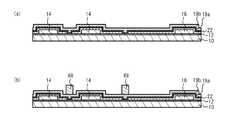
図2(b)に示すように、フォトレジスト45の上面および開口部46内の半導体層12の上面に半導体層12側から第1金属層であるNi(ニッケル)膜19a(膜厚が50nm)、その上に第3金属層であるAu(金)膜19b(膜厚が400nm)を例えば蒸着法を用い形成する。フォトレジスト45を除去することにより、Ni膜19aからなるゲート電極のパターンおよびNi膜19aからなる受けパターンを同時に形成する。これにより、ゲート電極18(ゲート電極パターン)および金属層20(受けパターン)が同時に形成される。ソース電極14およびドレイン電極16はゲート電極18を挟むように形成される。図2(c)に示すように、絶縁膜22上にゲート電極18および金属層20を覆うように絶縁膜24を形成する。絶縁膜24は、例えばCVD法を用い形成された窒化シリコン膜である。 As shown in FIG. 2B, a Ni (nickel)
図2(d)に示すように、ソース電極14、ドレイン電極16および金属層20上の絶縁膜22および24に開口48を形成する。図2(e)に示すように、絶縁膜24上に開口52および54を有するフォトレジスト50を形成する。開口52は、ドレイン電極16上に形成され、開口54は、ソース電極14、金属層20、およびソース電極14と金属層20との間の領域上に形成される。 As shown in FIG. 2D,
図3(a)に示すように、開口52および54内並びにフォトレジスト50上にシード層26を形成する。シード層26は、例えばスパッタ法を用い形成され、半導体層12側からTi膜およびAu膜を含む。図3(b)に示すように、シード層26上に開口52および54を有するフォトレジスト58を形成する。図3(c)に示すように、フォトレジスト58をマスクに、シード層26上に金属層28を形成する。金属層28は、電解めっき法を用い形成されたAu膜である。電解めっきの際は、シード層26を介しめっきのための電流が供給される。フォトレジスト50を除去する。金属層28は、ソース電極14上と金属層20とが離間した領域(例えば金属層20の両側に配置されたソース電極14それぞれと金属層20との間の離間された領域)の上に連続して形成する。 As shown in FIG. 3A, the
図4(a)に示すように、シード層26を、金属層28をマスクに除去する。フォトレジスト50を除去する。これにより、ソース電極14および金属層20上に、ソース電極14および金属層20と電気的に接続される金属層30(第4金属層)がシード層26および金属層28とから形成される。また、ドレイン電極16上に、ドレイン電極16と電気的に接続されたドレイン配線32が形成される。図4(b)に示すように、基板10の半導体層12が形成された上面を表面保護膜62を介し基板60に貼り付ける。表面保護膜62は、例えばワックスまたは保護テープである。基板60は例えばガラス基板である。基板10の下面(基板10における半導体層12が形成された面と反対の面)を研磨する。これにより、基板10を薄くする。 As shown in FIG. 4A, the
図5(a)に示すように、基板10の下面上に開口66を有するマスク層64を形成する。マスク層64は例えばNi膜を含む。Ni膜を含むとは、例えば純ニッケル膜、またははニッケル膜に他の元素を含む金属層を指す。図5(b)に示すように、マスク層64をマスクに基板10および半導体層12をエッチングする。エッチングは、例えばフッ素系ガスおよび塩素系のガスを用いたドライエッチング法(例えばRIE(Reactive
Ion Etching)またはICP(Inductively Coupled Plasma)エッチング)を用いる。例えば、基板10のエッチングには、フッ化硫黄(SF6)ガスを用いる。基板10のエッチングガスとして、CF4、NF3などを用いることもできる。半導体層12のエッチングには、塩素(Cl2)ガスを用いる。半導体層12のエッチングガスとして、塩化ホウ素(BCl3)ガスまたは塩化ケイ素(SiCl4)ガスなどを用いることもできる。これにより、図5(b)に示すように、基板10および半導体層12に貫通孔34が形成される。例えば塩素系を用いたエッチングにおいては、Niはほとんどエッチングされない。よって、Ni膜19aが貫通孔34を形成するエッチングストッパとして機能する。これにより、貫通孔34は、Ni膜19aに接して形成される。このように、金属層20(受けパターン)をエッチングストッパとして、基板10の裏面から金属層20(受けパターン)に向かって基板10および半導体層12を貫通する貫通孔34を形成する。As shown in FIG. 5A, a
Ion Etching) or ICP (Inductively Coupled Plasma) etching. For example, sulfur fluoride (SF6 ) gas is used for etching the
図6(a)に示すように、マスク層64を除去する。貫通孔34内および基板10の下面上に背面金属層36(第2金属層)を形成する。背面金属層36は、例えばめっき法を用い形成されたAu膜である。図6(b)に示すように、表面保護膜62を除去することにより、基板60を基板10から剥離する。以上により、実施例1に係る半導体装置100が完成する。 As shown in FIG. 6A, the
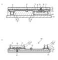
図7は、半導体装置のフィンガを示す平面図である。図7においては、フィンガ同士を接続する接続部およびパッド等の図示を省略し、各フィンガおよび貫通孔を図示している。図7に示すように、半導体層12上には、複数のドレイン電極16、複数のゲート電極18、複数のソース電極14および複数の金属層20が形成されている。金属層20に接続する貫通孔34が設けられている。金属層20の両側にはソース電極14が形成されている。両ソース電極14の両外側にはゲート電極18が形成されている。さらに、ゲート電極18の外側にドレイン電極16が形成されている。各フィンガの幅Wは例えば300μm、ソース電極14の長さL2は例えば5μm、金属層20の長さL3は例えば80μm、金属層30の長さL1は例えば100μmである。 FIG. 7 is a plan view showing the fingers of the semiconductor device. In FIG. 7, illustration of connection portions and pads for connecting the fingers together is omitted, and each finger and the through hole are illustrated. As shown in FIG. 7, a plurality of
実施例1によれば、図2(b)に示すように、半導体層12上に、Ni膜19aを含むゲート電極18を形成する工程と、半導体層12上にNi膜19aを含む金属層20を形成する工程と、を同時に実行する。このように、基板10および半導体層12に貫通孔34を形成する際のエッチングストッパであり、ソース電極14と電気的に接続される金属層20を、ゲート電極18と同時に形成する。これにより、金属層20は、ゲート電極18と同じ材料からなる。例えば、金属層20の各層の膜厚および材料はゲート電極18と同じである。よって、金属層20を形成する製造工程を簡略化できる。 According to the first embodiment, as shown in FIG. 2B, the step of forming the
なお、実施例1においては、第1金属層としてNi膜19aを例に説明したが、第1金属層は、ニッケルを含む単一の層であればよい。例えば、第1金属層は、純ニッケル膜、またはニッケル膜に他の元素を含む金属層でもよい。これにより、第1金属層を貫通孔34を形成する際のエッチングストッパとして用いることができる。また、Ni膜19aを半導体層12とのショットキー接合を形成する金属層として用いることができる。 In the first embodiment, the
さらに、金属層20(Ni膜19a、Au膜19b)をゲート電極18と同時に形成する。すなわち、第1金属層(Ni19a)からなるゲート電極パターンと受けパターンとを同時に形成する際に、第1金属層(Ni19a)および第3金属層(Au膜19b)からなるゲート電極パターンと受けパターンとを同時に形成する。これにより、金属層20とソース電極14との膜厚を同程度にすることができる。よって、金属層20およびソース電極14上に形成する絶縁膜24を段差なく形成することができ、金属層28を平坦に形成することもできる。なお、金属層20およびゲート電極18として、Ni膜19aを単層で形成することもできる。しかしながら、この場合、Ni膜19aとソース電極14との膜厚が異なるため、金属層28を平坦に形成することが難しくなる。このため、金属層20およびゲート電極18を形成する場合には、Ni膜19aおよびAu膜19bを連続して形成し、金属層20とゲート電極18との膜厚を同じ膜厚にすることが好ましい。また、第3金属層はAu膜以外でもよい。第3金属層は、ゲート電極の低抵抗層としても用いるため、第1金属層より低抵抗率の材料であることが好ましい。 Further, the metal layer 20 (
図4(a)に示すように、金属層30は、ソース電極14と、金属層20と、ソース電極14と金属層20とが離間した領域と、の上に連続して形成される。金属層30は、ソース電極14および金属層20に電気的に接続される。これにより、ソース電極14と金属層20との間を一体に形成することができる。また、金属層20とソース電極14とが電気的に接続され、貫通孔34の内部に背面金属層36が形成されている。これにより、ソース電極14と背面金属層36とを電気的に接続することができる。よって、ソースインダクタンスを低減できる。 As shown in FIG. 4A, the
図2(d)に示すように、ソース電極14と金属層20とは重なっていない。これにより、ソース電極14と金属層20との上面がほぼ平面となる。よって、図2(e)に示すように、フォトレジスト50に開口54を設ける際に開口54内にフォトレジスト50が残存することを抑制できる。このように、図2(d)以降の製造工程が容易となる。さらに、図4(a)において、金属層30の上面を平坦化できる。 As shown in FIG. 2D, the
図2(d)に示すように、ソース電極14と金属層20とは離間していてもよい。この場合、ソース電極14と金属層20との間には他の金属層が形成されていないことが好ましい。これにより、ソース電極14と金属層20との距離を小さくできる。さらに、ソース電極14と金属層20との間には絶縁膜22および24が形成されていることが好ましい。これにより、金属層30上をより平坦化できる。さらに、平坦化のためには、前述の通り、ソース電極14と金属層20との上面はほぼ同じ高さであることが好ましい。 As shown in FIG. 2D, the
図7のように、ソース電極14、ゲート電極18およびドレイン電極16は金属層20の両側に形成されている。このように、マルチフィンガタイプのFETにおいて、ソース電極14に隣接する金属層20を貫通孔34を介し接地できる。さらに、ソース電極14と金属層20とは、金属層30により電気的に接続される。これにより、ソース電極14をインダクタンスの影響が少なく接地できる。かつ、マルチフィンガFETの面積を小さくできる。 As shown in FIG. 7, the
図5(b)に示すように、貫通孔34は、基板10における半導体層12が形成された面と反対の面から基板10および半導体層12をエッチングすることにより形成する。この際、Ni膜19aがエッチングストッパとなる。 As shown in FIG. 5B, the through
図8(a)から図8(c)は、実施例1の変形例1を示す平面図である。図8(a)に示すように、金属層20の両側にソース電極14が形成されていてもよい。図8(b)に示すように、ソース電極14は金属層20を囲むように形成されていてもよい。図8(c)に示すように、金属層20は、楕円様形状でもよい。このように、金属層20の形状は四角でも楕円でも他の形状でもよい。ソース電極14は金属層20の少なくと一方に設けられていればよい。また、図示しないが、図8(a)から図8(c)に示すように、金属層20の両側にソース電極14が設けられることにより、図7に示すように、マルチフィンガタイプのFETに適用することができる。 FIG. 8A to FIG. 8C are plan views showing a first modification of the first embodiment. As shown in FIG. 8A, the
なお、実施例1は、金属層20をソース電極14に形成する例であるが、それ以外に、金属層20をソースパッドに形成することもできる(図示なし)。さらに、金属層20をドレイン電極16、ドレインパッドあるいはゲートパッドに形成することもできる(図示なし)。 In addition, although Example 1 is an example in which the
図8(a)から図8(c)の平面において、貫通孔34は、金属層20に含まれるように形成されることが好ましい。これにより、貫通孔34を形成する際に、金属層20以外がエッチングされることを抑制できる。 In the plane of FIG. 8A to FIG. 8C, the through
図9(a)および図9(b)は、実施例1の変形例2を示す断面図である。図9(a)を参照し、実施例1の図1(e)の後、フォトレジスト44を除去する。絶縁膜22の上面および開口46内の半導体層12の上面にNi膜19a(第1金属層)、その上にAu膜19b(第3金属層)を、スパッタ法または蒸着法を用い形成する。図9(b)に示すように、ゲート電極パターンおよび受けパターンを形成するためのフォトレジストパターン68を形成する。フォトレジストパターン68をマスクにAu膜19bおよびN1膜19aをエッチングする。Ni膜のエッチャントとしては例えば硝酸を用いる。これにより、図2(b)に示すように、Ni膜19aからなるゲート電極のパターンと受けパターンとが同時に形成される。その他の工程は実施例1と同じであり説明を省略する。実施例2の変形例2によっても、製造工程を削減できる。このように、蒸着法およびリフトオフ法以外の方法を用いゲート電極のパターンと受けパターンとを形成することもできる。 FIG. 9A and FIG. 9B are cross-sectional views showing a second modification of the first embodiment. Referring to FIG. 9A, the photoresist 44 is removed after FIG. 1E of the first embodiment. An
実施例1およびその変形例において、基板10は炭化シリコン基板、サファイア基板または窒化ガリウム基板であることが好ましい。このような基板10は、エッチングレートが遅い。よって、ほとんどエッチングされないNi膜19aを貫通孔34形成の際のエッチングストッパとして用いる。よって、ゲート電極18と同じ材料により金属層20を形成できる。 In Example 1 and its modifications, the
また、半導体層12は窒化物半導体層であることが好ましい。窒化物半導体を用いたFETにおいては、Ni膜19aをゲート電極18のショットキー接合を形成する金属層として用いることができる。よって、金属層20とゲート電極18とを同時に形成することができる。なお、窒化物半導体層は、例えばGaN層、InN層、AlN層、InGaN層、AlGaN層、InAlN層およびInAlGaN層の少なくとも一層を含む層とすることができる。 The
以上、本発明の実施例について詳述したが、本発明はかかる特定の実施例に限定されるものではなく、特許請求の範囲に記載された本発明の要旨の範囲内において、種々の変形・変更が可能である。 Although the embodiments of the present invention have been described in detail above, the present invention is not limited to such specific embodiments, and various modifications and changes can be made within the scope of the gist of the present invention described in the claims. It can be changed.
10 基板
12 半導体層
14 ソース電極
16 ドレイン電極
18 ゲート電極
19a Ni膜
19b Au膜
20 金属層
30 金属層
34 貫通孔
36 背面金属層DESCRIPTION OF
Claims (7)
Translated fromJapanese前記半導体層の上面にニッケルを含む単一の第1金属層を形成する工程と、
前記ソース電極および前記ドレイン電極に挟まれる位置に前記第1金属層からなるゲート電極のパターンと、前記ゲート電極のパターンとは離間し、かつ両側に位置する前記ソース電極とは離間した位置に前記第1金属層からなる受けパターンと、を同時に形成する工程と、
前記受けパターンをエッチングストッパとして、前記基板の下面から前記受けパターンに向かって前記基板および前記半導体層を貫通する貫通孔を形成するエッチング工程と、
前記受けパターンの上面および前記ソース電極の上面に接触し、前記両側のソース電極のうち一方から他方にかけて連続し、かつ前記受けパターンと前記両側のソース電極とを覆う第4金属層を形成する工程と、を含むことを特徴とする半導体装置の製造方法。Forming a source electrode and a drain electrode on the semiconductor layer formed on the upper surface of the substrate;
Forming a single first metal layer containing nickel on an upper surface of the semiconductor layer;
The pattern of the gate electrode made of the first metal layer and the pattern of the gate electrode are separated from each other between thesource electrode and the drain electrode, and the source electrode located on both sides is separated fromthe source electrode. Forming a receiving pattern made of the first metal layer at the same time;
Using the receiving pattern as an etching stopper, an etching step of forming a through-hole penetrating the substrate and the semiconductor layer from the lower surface of the substrate toward the receiving pattern;
Forming a fourth metal layer in contact with the upper surface of the receiving pattern and the upper surface of the source electrode, continuous from one to the other of the source electrodes on both sides, and covering the receiving pattern and the source electrodes on both sides A method of manufacturing a semiconductor device, comprising:
前記半導体層上に前記ソース電極および前記ドレイン電極に挟まれる位置にゲート電極の開口を備え、前記ゲート電極のパターンとは離間し、かつ両側に位置する前記ソース電極とは離間した位置に受けパターンの開口を備えた開口部を有する樹脂層からなるマスクを形成する工程と、
前記マスクの上面および前記開口部内の半導体層の上面にニッケルを含む単一の第1金属層を形成する工程と、
前記マスクを除去することで、前記ソース電極および前記ドレイン電極に挟まれる位置に前記第1金属層からなるゲート電極のパターンと、前記ゲート電極のパターンとは離間した位置に前記第1金属層からなる前記受けパターンと、を同時に形成する工程と、
前記受けパターンをエッチングストッパとして、前記基板の下面から受けパターンに向かって前記基板および前記半導体層を貫通する貫通孔を形成するエッチング工程と、
前記受けパターンの上面および前記ソース電極の上面に接触し、前記両側のソース電極のうち一方から他方にかけて連続し、かつ前記受けパターンと前記両側のソース電極とを覆う第4金属層を形成する工程と、を含むことを特徴とする半導体装置の製造方法。Forming a source electrode and a drain electrode on the semiconductor layer formed on the upper surface of the substrate;
A gate electrode opening is provided at a position sandwiched between the source electrode and the drain electrode on the semiconductor layer, spaced from the gate electrode pattern, and a receiving patternspaced from the source electrode located on both sides. Forming a mask made of a resin layer having an opening with a plurality of openings;
Forming a single first metal layer containing nickel on the upper surface of the mask and the upper surface of the semiconductor layer in the opening;
By removing the mask, the pattern of the gate electrode made of the first metal layer at a position sandwiched between the source electrode and the drain electrode and the pattern of the gate electrode are separated from the first metal layer. The step of simultaneously forming the receiving pattern,
Using the receiving pattern as an etching stopper, an etching process for forming a through hole penetrating the substrate and the semiconductor layer from the lower surface of the substrate toward the receiving pattern;
Forming a fourth metal layer in contact with the upper surface of the receiving pattern and the upper surface of the source electrode, continuous from one to the other of the source electrodes on both sides, and covering the receiving pattern and the source electrodes on both sides A method of manufacturing a semiconductor device, comprising:
前記マスクの前記開口部は、前記絶縁膜の開口部の幅よりも広く、且つ前記マスクの開口部の内側に前記絶縁膜の開口部を含んでなり、
前記第4金属層は、前記両側のソース電極のうち一方から他方にかけて、前記絶縁膜を介して前記受けパターンと前記両側のソース電極とを覆うことを特徴とする請求項2記載の半導体装置の製造方法。Prior to the step of forming the mask, an insulating film having openings in the region between thesource electrodes andthe region between thesource electrode and the drain electrodeis formed on the semiconductor layerand the source electrode. Further comprising a step,
The opening of the mask is wider than the width of the opening portion of the insulating film,Ri and Na include openings of the insulating film inside the opening of themask,
3. The semiconductor device according to claim 2,wherein the fourth metal layer covers the receiving pattern and the source electrodes on both sides through the insulating film from one to the other of the source electrodes on both sides . Production method.
前記第1金属層からなる前記ゲート電極のパターンと前記第1金属層からなる前記受けパターンとを同時に形成する工程は、前記第1金属層および前記第3金属層からなる前記ゲート電極のパターンと前記第1金属層および前記第3金属層からなる前記受けパターンとを同時に形成する工程を含むことを特徴とする請求項1または2記載の半導体装置の製造方法。Forming a third metal layer on the first metal layer;
The step of simultaneously forming the pattern of the gate electrode made of the first metal layer and the receiving pattern made of the first metal layer includes the step of forming the pattern of the gate electrode made of the first metal layer and the third metal layer. 3. The method of manufacturing a semiconductor device according to claim 1, further comprising the step of simultaneously forming the receiving pattern comprising the first metal layer and the third metal layer.
前記第4金属層は、前記両側のソース電極のうち一方から他方にかけて、前記絶縁膜を介して前記受けパターンと前記両側のソース電極とを覆う請求項1記載の半導体装置の製造方法。Further comprising forming an insulating film on the semiconductor layer and the source electrode;
2. The method of manufacturinga semiconductor device according toclaim 1, wherein the fourth metal layer covers the receiving pattern and the source electrodes on both sides through the insulating film from one to the other of the source electrodes on both sides .
Priority Applications (1)
| Application Number | Priority Date | Filing Date | Title |
|---|---|---|---|
| JP2012113799AJP6003213B2 (en) | 2012-05-17 | 2012-05-17 | Manufacturing method of semiconductor device |
Applications Claiming Priority (1)
| Application Number | Priority Date | Filing Date | Title |
|---|---|---|---|
| JP2012113799AJP6003213B2 (en) | 2012-05-17 | 2012-05-17 | Manufacturing method of semiconductor device |
Publications (2)
| Publication Number | Publication Date |
|---|---|
| JP2013243173A JP2013243173A (en) | 2013-12-05 |
| JP6003213B2true JP6003213B2 (en) | 2016-10-05 |
Family
ID=49843807
Family Applications (1)
| Application Number | Title | Priority Date | Filing Date |
|---|---|---|---|
| JP2012113799AActiveJP6003213B2 (en) | 2012-05-17 | 2012-05-17 | Manufacturing method of semiconductor device |
Country Status (1)
| Country | Link |
|---|---|
| JP (1) | JP6003213B2 (en) |
Families Citing this family (2)
| Publication number | Priority date | Publication date | Assignee | Title |
|---|---|---|---|---|
| JP6436531B2 (en) | 2015-01-30 | 2018-12-12 | 住友電工デバイス・イノベーション株式会社 | Manufacturing method of semiconductor device |
| JP7459973B2 (en)* | 2020-12-22 | 2024-04-02 | 三菱電機株式会社 | Semiconductor device and its manufacturing method |
Family Cites Families (4)
| Publication number | Priority date | Publication date | Assignee | Title |
|---|---|---|---|---|
| JP2004056031A (en)* | 2002-07-24 | 2004-02-19 | Mitsubishi Electric Corp | Semiconductor device |
| JP5487590B2 (en)* | 2008-10-20 | 2014-05-07 | 富士通株式会社 | Semiconductor device and manufacturing method thereof |
| JP5604855B2 (en)* | 2009-11-17 | 2014-10-15 | 富士通株式会社 | Semiconductor device and manufacturing method thereof |
| JP5970736B2 (en)* | 2012-04-27 | 2016-08-17 | 住友電工デバイス・イノベーション株式会社 | Manufacturing method of semiconductor device |
- 2012
- 2012-05-17JPJP2012113799Apatent/JP6003213B2/enactiveActive
Also Published As
| Publication number | Publication date |
|---|---|
| JP2013243173A (en) | 2013-12-05 |
Similar Documents
| Publication | Publication Date | Title |
|---|---|---|
| JP4516538B2 (en) | Manufacturing method of semiconductor device | |
| US9368609B2 (en) | Semiconductor device including a trench with a corner having plural tapered portions | |
| CN109698236B (en) | Semiconductor device | |
| US9484446B2 (en) | Semiconductor device and method for manufacturing the same | |
| JP6240460B2 (en) | Field effect type compound semiconductor device and manufacturing method thereof | |
| CN110896099B (en) | Semiconductor device with a semiconductor layer having a plurality of semiconductor layers | |
| JP6981601B2 (en) | Manufacturing method of semiconductor device | |
| JP5649357B2 (en) | Semiconductor device and manufacturing method | |
| CN112928161B (en) | High electron mobility transistor and manufacturing method thereof | |
| JP2018037497A (en) | Semiconductor device | |
| US11476110B2 (en) | Semiconductor device | |
| CN112652659B (en) | High electron mobility transistor and manufacturing method thereof | |
| TWI653742B (en) | Semiconductor device and method of manufacturing same | |
| JP6171250B2 (en) | Semiconductor device | |
| JP6003213B2 (en) | Manufacturing method of semiconductor device | |
| JP7215800B2 (en) | Semiconductor device manufacturing method and semiconductor device | |
| CN106449773B (en) | GaN-based Schottky diode structure and manufacturing method thereof | |
| TW202115909A (en) | High electron mobility transistor and method for fabricating the same | |
| JP2010097974A (en) | Compound semiconductor field effect transistor and method of manufacturing the same | |
| TW201937730A (en) | Semiconductor device | |
| US20140339568A1 (en) | Semiconductor device with substrate via hole and method to form the same | |
| JP2017208379A (en) | Nitride semiconductor device | |
| JP5386810B2 (en) | MIS FET and manufacturing method thereof | |
| JP5700502B2 (en) | Semiconductor device and manufacturing method | |
| JP2009267358A (en) | Semiconductor device |
Legal Events
| Date | Code | Title | Description |
|---|---|---|---|
| A621 | Written request for application examination | Free format text:JAPANESE INTERMEDIATE CODE: A621 Effective date:20150416 | |
| A977 | Report on retrieval | Free format text:JAPANESE INTERMEDIATE CODE: A971007 Effective date:20151221 | |
| A131 | Notification of reasons for refusal | Free format text:JAPANESE INTERMEDIATE CODE: A131 Effective date:20160105 | |
| A521 | Request for written amendment filed | Free format text:JAPANESE INTERMEDIATE CODE: A523 Effective date:20160307 | |
| TRDD | Decision of grant or rejection written | ||
| A01 | Written decision to grant a patent or to grant a registration (utility model) | Free format text:JAPANESE INTERMEDIATE CODE: A01 Effective date:20160809 | |
| A61 | First payment of annual fees (during grant procedure) | Free format text:JAPANESE INTERMEDIATE CODE: A61 Effective date:20160822 | |
| R150 | Certificate of patent or registration of utility model | Ref document number:6003213 Country of ref document:JP Free format text:JAPANESE INTERMEDIATE CODE: R150 | |
| R250 | Receipt of annual fees | Free format text:JAPANESE INTERMEDIATE CODE: R250 | |
| R250 | Receipt of annual fees | Free format text:JAPANESE INTERMEDIATE CODE: R250 | |
| R250 | Receipt of annual fees | Free format text:JAPANESE INTERMEDIATE CODE: R250 | |
| R250 | Receipt of annual fees | Free format text:JAPANESE INTERMEDIATE CODE: R250 | |
| R250 | Receipt of annual fees | Free format text:JAPANESE INTERMEDIATE CODE: R250 | |
| R250 | Receipt of annual fees | Free format text:JAPANESE INTERMEDIATE CODE: R250 | |
| R250 | Receipt of annual fees | Free format text:JAPANESE INTERMEDIATE CODE: R250 |