JP5986392B2 - Semiconductor device - Google Patents
Semiconductor deviceDownload PDFInfo
- Publication number
- JP5986392B2 JP5986392B2JP2012034637AJP2012034637AJP5986392B2JP 5986392 B2JP5986392 B2JP 5986392B2JP 2012034637 AJP2012034637 AJP 2012034637AJP 2012034637 AJP2012034637 AJP 2012034637AJP 5986392 B2JP5986392 B2JP 5986392B2
- Authority
- JP
- Japan
- Prior art keywords
- gate electrode
- transistor
- film
- insulating film
- semiconductor film
- Prior art date
- Legal status (The legal status is an assumption and is not a legal conclusion. Google has not performed a legal analysis and makes no representation as to the accuracy of the status listed.)
- Expired - Fee Related
Links
Images


Classifications
- G—PHYSICS
- G11—INFORMATION STORAGE
- G11C—STATIC STORES
- G11C11/00—Digital stores characterised by the use of particular electric or magnetic storage elements; Storage elements therefor
- G11C11/21—Digital stores characterised by the use of particular electric or magnetic storage elements; Storage elements therefor using electric elements
- G11C11/34—Digital stores characterised by the use of particular electric or magnetic storage elements; Storage elements therefor using electric elements using semiconductor devices
- G11C11/40—Digital stores characterised by the use of particular electric or magnetic storage elements; Storage elements therefor using electric elements using semiconductor devices using transistors
- G11C11/401—Digital stores characterised by the use of particular electric or magnetic storage elements; Storage elements therefor using electric elements using semiconductor devices using transistors forming cells needing refreshing or charge regeneration, i.e. dynamic cells
- G11C11/403—Digital stores characterised by the use of particular electric or magnetic storage elements; Storage elements therefor using electric elements using semiconductor devices using transistors forming cells needing refreshing or charge regeneration, i.e. dynamic cells with charge regeneration common to a multiplicity of memory cells, i.e. external refresh
- G11C11/404—Digital stores characterised by the use of particular electric or magnetic storage elements; Storage elements therefor using electric elements using semiconductor devices using transistors forming cells needing refreshing or charge regeneration, i.e. dynamic cells with charge regeneration common to a multiplicity of memory cells, i.e. external refresh with one charge-transfer gate, e.g. MOS transistor, per cell
- H—ELECTRICITY
- H10—SEMICONDUCTOR DEVICES; ELECTRIC SOLID-STATE DEVICES NOT OTHERWISE PROVIDED FOR
- H10B—ELECTRONIC MEMORY DEVICES
- H10B12/00—Dynamic random access memory [DRAM] devices
- H10B12/01—Manufacture or treatment
- H10B12/02—Manufacture or treatment for one transistor one-capacitor [1T-1C] memory cells
- H10B12/05—Making the transistor
- H—ELECTRICITY
- H10—SEMICONDUCTOR DEVICES; ELECTRIC SOLID-STATE DEVICES NOT OTHERWISE PROVIDED FOR
- H10B—ELECTRONIC MEMORY DEVICES
- H10B41/00—Electrically erasable-and-programmable ROM [EEPROM] devices comprising floating gates
- H10B41/70—Electrically erasable-and-programmable ROM [EEPROM] devices comprising floating gates the floating gate being an electrode shared by two or more components
- H—ELECTRICITY
- H10—SEMICONDUCTOR DEVICES; ELECTRIC SOLID-STATE DEVICES NOT OTHERWISE PROVIDED FOR
- H10D—INORGANIC ELECTRIC SEMICONDUCTOR DEVICES
- H10D30/00—Field-effect transistors [FET]
- H10D30/60—Insulated-gate field-effect transistors [IGFET]
- H10D30/67—Thin-film transistors [TFT]
- H10D30/6729—Thin-film transistors [TFT] characterised by the electrodes
- H10D30/673—Thin-film transistors [TFT] characterised by the electrodes characterised by the shapes, relative sizes or dispositions of the gate electrodes
- H—ELECTRICITY
- H10—SEMICONDUCTOR DEVICES; ELECTRIC SOLID-STATE DEVICES NOT OTHERWISE PROVIDED FOR
- H10D—INORGANIC ELECTRIC SEMICONDUCTOR DEVICES
- H10D30/00—Field-effect transistors [FET]
- H10D30/60—Insulated-gate field-effect transistors [IGFET]
- H10D30/67—Thin-film transistors [TFT]
- H10D30/6729—Thin-film transistors [TFT] characterised by the electrodes
- H10D30/6737—Thin-film transistors [TFT] characterised by the electrodes characterised by the electrode materials
- H10D30/6739—Conductor-insulator-semiconductor electrodes
- H—ELECTRICITY
- H10—SEMICONDUCTOR DEVICES; ELECTRIC SOLID-STATE DEVICES NOT OTHERWISE PROVIDED FOR
- H10D—INORGANIC ELECTRIC SEMICONDUCTOR DEVICES
- H10D30/00—Field-effect transistors [FET]
- H10D30/60—Insulated-gate field-effect transistors [IGFET]
- H10D30/67—Thin-film transistors [TFT]
- H10D30/674—Thin-film transistors [TFT] characterised by the active materials
- H10D30/6755—Oxide semiconductors, e.g. zinc oxide, copper aluminium oxide or cadmium stannate
- H—ELECTRICITY
- H10—SEMICONDUCTOR DEVICES; ELECTRIC SOLID-STATE DEVICES NOT OTHERWISE PROVIDED FOR
- H10D—INORGANIC ELECTRIC SEMICONDUCTOR DEVICES
- H10D86/00—Integrated devices formed in or on insulating or conducting substrates, e.g. formed in silicon-on-insulator [SOI] substrates or on stainless steel or glass substrates
- H10D86/01—Manufacture or treatment
- H—ELECTRICITY
- H10—SEMICONDUCTOR DEVICES; ELECTRIC SOLID-STATE DEVICES NOT OTHERWISE PROVIDED FOR
- H10D—INORGANIC ELECTRIC SEMICONDUCTOR DEVICES
- H10D86/00—Integrated devices formed in or on insulating or conducting substrates, e.g. formed in silicon-on-insulator [SOI] substrates or on stainless steel or glass substrates
- H10D86/201—Integrated devices formed in or on insulating or conducting substrates, e.g. formed in silicon-on-insulator [SOI] substrates or on stainless steel or glass substrates the substrates comprising an insulating layer on a semiconductor body, e.g. SOI
Landscapes
- Engineering & Computer Science (AREA)
- Microelectronics & Electronic Packaging (AREA)
- Computer Hardware Design (AREA)
- Manufacturing & Machinery (AREA)
- Thin Film Transistor (AREA)
- Electrodes Of Semiconductors (AREA)
- Semiconductor Memories (AREA)
- Non-Volatile Memory (AREA)
- Liquid Crystal (AREA)
Description
Translated fromJapaneseトランジスタなどの半導体素子を含む回路を有する半導体装置に関する。例えば、電源回路に搭載されるパワーデバイス、メモリ、サイリスタ、コンバータ、イメージセンサなどを含む半導体集積回路、液晶表示パネルに代表される電気光学装置、および発光素子を有する発光表示装置、ならびにそれらを部品として搭載した電子機器に関する。The present invention relates to a semiconductor device having a circuit including a semiconductor element such as a transistor. For example, a semiconductor integrated circuit including a power device, a memory, a thyristor, a converter, and an image sensor mounted on a power supply circuit, an electro-optical device typified by a liquid crystal display panel, and a light-emitting display device having a light-emitting element, and components thereof It is related with the electronic equipment carried as.
なお、本明細書中において半導体装置とは、半導体特性を利用する装置全般を指し、半導体記憶装置、電気光学装置、発光表示装置、半導体回路および電子機器は全て半導体装置である。Note that in this specification, a semiconductor device refers to all devices that use semiconductor characteristics, and a semiconductor memory device, an electro-optical device, a light-emitting display device, a semiconductor circuit, and an electronic device are all semiconductor devices.
半導体記憶装置としてDRAM(Dynamic Random Access Memory)はよく知られた製品であり、今日においても各種電子機器の中で使われている。DRAMの中核部を構成するメモリセルは書き込みおよび読み出し用のトランジスタとキャパシタによって構成されている。A DRAM (Dynamic Random Access Memory) is a well-known product as a semiconductor memory device and is used in various electronic devices today. A memory cell constituting the core of the DRAM is composed of a write and read transistor and a capacitor.
DRAMは、他の半導体集積回路と同様にスケーリング則に従って回路パターンの微細化が進められてきたが、デザインルールを100nm以下にすることは難しいと考えられていた時期もあった。その理由の一つとして、トランジスタのチャネル長が100nm以下となると、短チャネル効果によりパンチスルー電流が流れやすくなり、トランジスタがスイッチング素子として機能しなくなるということがある。パンチスルー電流を防ぐには、シリコンウェハに高濃度の不純物をドーピングすればよいが、そうするとソースとウェハ間またはドレインとウェハ間に接合リーク電流が流れやすくなり、結局はメモリの保持特性を低下させてしまう原因となってしまい、この問題の解決策としては適切ではなかった。In DRAMs, circuit patterns have been miniaturized according to scaling rules as in other semiconductor integrated circuits, but there were times when it was considered difficult to make the
このような問題に対して、メモリセルを構成するトランジスタを三次元に形成し、一つのメモリセルが占める面積を縮小しつつ、トランジスタのチャネル長を短チャネル効果が生じない程度に維持する方法が考えられてきた。例えば、トランジスタのチャネル部が形成される領域にU字状の縦長溝を形成し、その溝の壁面に沿ってゲート絶縁膜を形成し、さらにその溝にゲート電極を埋め込んだ構造が開示されている(非特許文献1参照。)。In order to solve such a problem, there is a method in which a transistor constituting a memory cell is formed three-dimensionally and the channel length of the transistor is maintained to such an extent that the short channel effect does not occur while reducing the area occupied by one memory cell. Has been considered. For example, a structure is disclosed in which a U-shaped vertical groove is formed in a region where a channel portion of a transistor is formed, a gate insulating film is formed along a wall surface of the groove, and a gate electrode is embedded in the groove. (See Non-Patent Document 1).
このような構造をチャネル部に有するトランジスタは、ソース領域とドレイン領域の間を流れる電流が溝部分を回り込む形で流れるためチャネル長が長くなっている。このため、トランジスタの占有面積を縮小しつつ、短チャネル効果を抑制できるといった効果を奏する。A transistor having such a structure in the channel portion has a long channel length because a current flowing between the source region and the drain region flows around the groove portion. As a result, the short channel effect can be suppressed while reducing the area occupied by the transistor.
しかしながら、トランジスタのチャネル部が形成される領域にU字状の縦長溝を形成する方法は、溝を掘るためにフォトリソグラフィ工程を余分に行う必要があり、コストや歩留まりの観点で問題があった。However, the method of forming a U-shaped vertical groove in the region where the channel portion of the transistor is formed requires an extra photolithography step to dig the groove, which is problematic in terms of cost and yield. .
また、縦長溝に対してゲート絶縁膜などを成膜する場合、スパッタリング法やプラズマCVD(Chemical Vapor Deposition)法では、溝の入り口付近で膜の堆積量が増加し、溝が成膜材料で塞がってしまうことがあった。そのため、被覆性の高い成膜方法を選定する必要があった。具体的には、比較的コスト高となる原子層堆積法(ALD:Atomic Layer Deposition)法、またはシリコンウェハなどでしか使用できない熱酸化法などに限られる問題があった。In addition, when a gate insulating film or the like is formed in a vertically long groove, in the sputtering method or plasma CVD (Chemical Vapor Deposition) method, the deposition amount of the film increases near the entrance of the groove, and the groove is blocked with a film forming material. There was a case. Therefore, it was necessary to select a film forming method with high coverage. Specifically, there is a problem that is limited to an atomic layer deposition (ALD) method, which is relatively expensive, or a thermal oxidation method that can be used only on a silicon wafer.
そこで、縦長溝を用いずに、見かけ上のチャネル長に対して、チャネル長を長くする構造を提供する。Therefore, a structure is provided in which the channel length is increased with respect to the apparent channel length without using the longitudinal groove.
本発明の一態様は、三次元形状のチャネル領域を形成することにより、上面から見た一対の電極間距離である見かけ上のチャネル長Lに対して、チャネル長L’が3倍以上、好ましくは5倍以上、さらに好ましくは10倍以上の長さとするようにゲート電極または絶縁表面を有する構造物を基板上に設けることを技術的思想とする。In one embodiment of the present invention, by forming a channel region having a three-dimensional shape, the channel length L ′ is preferably three times or more the apparent channel length L that is the distance between a pair of electrodes as viewed from above. The technical idea is to provide a gate electrode or a structure having an insulating surface on the substrate so that the length is 5 times or more, more preferably 10 times or more.
本発明の一態様は、ゲート電極と、ゲート電極を覆うゲート絶縁膜と、ゲート絶縁膜上にあり、かつ少なくとも一部がゲート電極と重畳する半導体膜と、半導体膜と接し、かつゲート電極と重畳しない一対の電極と、を有し、上面から見た一対の電極間距離である見かけ上のチャネル長Lに対して、チャネル長L’が3倍以上、好ましくは5倍以上、さらに好ましくは10倍以上の長さである半導体装置である。One embodiment of the present invention includes a gate electrode, a gate insulating film that covers the gate electrode, a semiconductor film over the gate insulating film and at least part of which overlaps with the gate electrode, in contact with the semiconductor film, and the gate electrode The channel length L ′ is 3 times or more, preferably 5 times or more, more preferably, more than the apparent channel length L, which is the distance between the pair of electrodes as viewed from above. It is a semiconductor device having a length of 10 times or more.
また、第1のゲート電極と、第1のゲート電極に重畳し、第1のゲート電極よりも上面形状の小さい第2のゲート電極と、第1のゲート電極および第2のゲート電極を覆うゲート絶縁膜と、ゲート絶縁膜上にあり、かつ少なくとも一部が第2のゲート電極と重畳する半導体膜と、半導体膜と接し、第1のゲート電極と重畳し、かつ第2のゲート電極と重畳しない一対の電極と、を有する半導体装置である。なお、第1のゲート電極および第2のゲート電極を同一材料としても構わない。In addition, the first gate electrode, the second gate electrode overlapping with the first gate electrode and having a smaller top surface shape than the first gate electrode, and the gate covering the first gate electrode and the second gate electrode An insulating film; a semiconductor film which is over the gate insulating film and at least partially overlaps with the second gate electrode; and is in contact with the semiconductor film, overlaps with the first gate electrode, and overlaps with the second gate electrode And a pair of electrodes that are not. Note that the first gate electrode and the second gate electrode may be made of the same material.
また、絶縁表面を有する構造物と、少なくとも構造物の一部と重畳する半導体膜と、半導体膜と接し、かつ構造物と重畳しない一対の電極と、半導体膜を覆うゲート絶縁膜と、ゲート絶縁膜を介して半導体膜上のゲート電極と、を有し、上面から見た一対の電極間距離である見かけ上のチャネル長Lに対して、チャネル長L’が3倍以上、好ましくは5倍以上、さらに好ましくは10倍以上の長さである半導体装置である。A structure having an insulating surface; a semiconductor film overlapping with at least part of the structure; a pair of electrodes in contact with the semiconductor film and not overlapping with the structure; a gate insulating film covering the semiconductor film; and gate insulation The channel length L ′ is 3 times or more, preferably 5 times the apparent channel length L, which is the distance between the pair of electrodes as viewed from above. More preferably, the semiconductor device has a length of 10 times or more.
半導体膜は酸化物半導体膜または結晶シリコン膜(微結晶シリコン膜、多結晶シリコン膜など)を用いればよい。As the semiconductor film, an oxide semiconductor film or a crystalline silicon film (such as a microcrystalline silicon film or a polycrystalline silicon film) may be used.
絶縁表面を有する構造物の材料は、後の熱処理に耐える材料であればよく、例えば、酸化シリコン、酸化窒化シリコン、窒化酸化シリコン、窒化シリコン、酸化アルミニウム、酸化窒化アルミニウム、窒化酸化アルミニウム、窒化アルミニウムなどの無機化合物またはポリイミドなどの有機化合物を用いればよい。または、導電性を有する材料の表面を絶縁化処理して用いても構わない。The material of the structure having an insulating surface may be any material that can withstand heat treatment later. For example, silicon oxide, silicon oxynitride, silicon nitride oxide, silicon nitride, aluminum oxide, aluminum oxynitride, aluminum nitride oxide, aluminum nitride Inorganic compounds such as polyimide or organic compounds such as polyimide may be used. Alternatively, the surface of a conductive material may be used after being insulated.
酸化窒化シリコンとは、その組成において、窒素よりも酸素の含有量が多いものを示し、例えば、酸素が50atomic%以上70atomic%以下、窒素が0.5atomic%以上15atomic%以下、シリコンが25atomic%以上35atomic%以下、水素が0atomic%以上10atomic%以下の範囲で含まれるものをいう。また、窒化酸化シリコンとは、その組成において、酸素よりも窒素の含有量が多いものを示し、例えば、酸素が5atomic%以上30atomic%以下、窒素が20atomic%以上55atomic%以下、シリコンが25atomic%以上35atomic%以下、水素が10atomic%以上25atomic%以下の範囲で含まれるものをいう。但し、上記範囲は、ラザフォード後方散乱法(RBS:Rutherford Backscattering Spectrometry)や、水素前方散乱法(HFS:Hydrogen Forward scattering Spectrometry)を用いて測定した場合のものである。また、構成元素の組成は、その合計が100atomic%を超えない値をとる。Silicon oxynitride refers to a silicon oxynitride having a higher oxygen content than nitrogen. For example, oxygen is 50 atomic% to 70 atomic%, nitrogen is 0.5 atomic% to 15 atomic%, and silicon is 25 atomic% or more. 35 atomic% or less and hydrogen is included in the range of 0 atomic% to 10 atomic%. Silicon nitride oxide refers to a composition having a nitrogen content higher than that of oxygen. For example, oxygen is 5 atomic% to 30 atomic%, nitrogen is 20 atomic% to 55 atomic%, and silicon is 25 atomic% or more. 35 atomic% or less and hydrogen is included in the range of 10 atomic% or more and 25 atomic% or less. However, the above ranges are those measured using Rutherford Backscattering Spectrometry (RBS) or Hydrogen Forward Scattering Spectrometry (HFS). Further, the composition of the constituent elements takes a value that the total does not exceed 100 atomic%.
酸化窒化アルミニウムとは、その組成において、窒素よりも酸素の含有量が多いものを示す。また、窒化酸化アルミニウムとは、その組成において、酸素よりも窒素の含有量が多いものを示す。Aluminum oxynitride indicates a composition having a higher oxygen content than nitrogen. In addition, the aluminum oxynitride indicates a composition having a nitrogen content higher than that of oxygen.
本発明の一態様により、短チャネル効果の影響を低減し、かつ半導体装置を集積度を高めることが可能となる。また、コストが低く、歩留まりの高い半導体装置を提供することができる。According to one embodiment of the present invention, the influence of a short channel effect can be reduced and the degree of integration of a semiconductor device can be increased. In addition, a semiconductor device with low cost and high yield can be provided.
以下では、本発明の実施の形態について図面を用いて詳細に説明する。ただし、本発明は以下の説明に限定されず、その形態および詳細を様々に変更し得ることは、当業者であれば容易に理解される。また、本発明は以下に示す実施の形態の記載内容に限定して解釈されるものではない。なお、図面を用いて発明の構成を説明するにあたり、同じものを指す符号は異なる図面間でも共通して用いる。なお、同様のものを指す際にはハッチパターンを同じくし、特に符号を付さない場合がある。Hereinafter, embodiments of the present invention will be described in detail with reference to the drawings. However, the present invention is not limited to the following description, and it will be easily understood by those skilled in the art that modes and details can be variously changed. In addition, the present invention is not construed as being limited to the description of the embodiments below. Note that in describing the structure of the present invention with reference to drawings, the same portions are denoted by the same reference numerals in different drawings. In addition, when referring to the same thing, a hatch pattern is made the same and there is a case where it does not attach a code in particular.
以下、本発明の説明を行うが、本明細書で用いる用語について簡単に説明する。まず、トランジスタのソースとドレインについては、本明細書においては、一方をドレインと呼ぶとき他方をソースとする。すなわち、電位の高低によって、それらを区別しない。従って、本明細書において、ソースとされている部分をドレインと読み替えることもできる。Hereinafter, the present invention will be described, but terms used in this specification will be briefly described. First, regarding the source and drain of a transistor, in this specification, when one is called a drain, the other is a source. That is, they are not distinguished depending on the potential level. Therefore, in this specification, a portion which is a source can be read as a drain.
また、電圧とは、ある電位と、基準の電位(例えばグラウンド電位)との電位差のことを示す場合が多い。よって、電圧、電位、電位差を、各々、電位、電圧、電圧差と言い換えることが可能である。The voltage often indicates a potential difference between a certain potential and a reference potential (for example, a ground potential). Thus, voltage, potential, and potential difference can be referred to as potential, voltage, and voltage difference, respectively.
本明細書においては、「接続する」と表現される場合であっても、現実の回路においては、物理的な接続部分がなく、配線が延在している場合だけのこともある。In this specification, even when expressed as “connected”, in an actual circuit, there may be only a case where there is no physical connection portion and a wiring is extended.
なお、第1、第2として付される序数詞は便宜上用いるものであり、工程順または積層順を示すものではない。また、本明細書において発明を特定するための事項として固有の名称を示すものではない。The ordinal numbers attached as the first and second are used for convenience and do not indicate the order of steps or the order of lamination. In addition, a specific name is not shown as a matter for specifying the invention in this specification.
(実施の形態1)
本実施の形態では、本発明の一態様であるトランジスタの一例について図1を用いて説明する。(Embodiment 1)
In this embodiment, an example of a transistor which is one embodiment of the present invention will be described with reference to FIGS.
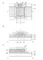
図1(A)はトランジスタの上面図である。図1(A)に示した一点鎖線A−Bおよび一点鎖線C−Dにおける断面は、それぞれ図1(B)に示すA−B断面および図1(C)に示すC−D断面に対応する。なお、図1(A)では、簡単のため保護絶縁膜118およびゲート絶縁膜112を省略して示す。FIG. 1A is a top view of a transistor. Cross sections taken along one-dot chain line AB and one-dot chain line CD shown in FIG. 1A correspond to the AB cross section shown in FIG. 1B and the CD cross section shown in FIG. 1C, respectively. . Note that in FIG. 1A, the protective
ここでは、図1(B)に示すA−B断面について詳細に説明する。Here, an AB cross section shown in FIG. 1B will be described in detail.
A−B断面は、基板100と、基板100上の第1のゲート電極104と、第1のゲート電極104上の第1のゲート電極104よりも上面形状の小さい第2のゲート電極105と、第1のゲート電極104および第2のゲート電極105を覆うゲート絶縁膜112と、ゲート絶縁膜112上にあり、かつ少なくとも一部が第2のゲート電極105と重畳する半導体膜106と、半導体膜106上にあり半導体膜106と一部が接する一対の電極116と、ゲート絶縁膜112、半導体膜106および一対の電極116を覆う保護絶縁膜118と、を有するトランジスタの断面である。なお、基板上に下地絶縁膜を設けても構わない。The A-B cross section includes a
第1のゲート電極104および第2のゲート電極105は、幅および高さを以下のように選択する。具体的には、第1のゲート電極104および第2のゲート電極105を用い、三次元形状のチャネル領域を形成することにより、一対の電極116間距離である見かけ上のチャネル長Lに対して、チャネル長L’を3倍以上、好ましくは5倍以上、さらに好ましくは10倍以上の長さとなるように幅および高さを選択すればよい。前述の範囲を満たすために、第2のゲート電極105の断面形状において、側面を形成する辺の長さの和が上面を形成する辺の長さの2倍以上としてもよい。The width and height of the
基板100に大きな制限はないが、少なくとも、後の熱処理に耐えうる程度の耐熱性を有している必要がある。例えば、ガラス基板、セラミック基板、石英基板、サファイア基板などを、基板100として用いてもよい。また、シリコンや炭化シリコンなどの単結晶半導体基板、多結晶半導体基板、シリコンゲルマニウムなどの化合物半導体基板、SOI(Silicon On Insulator)基板などを適用することも可能であり、これらの基板上に半導体素子が設けられたものを、基板100として用いてもよい。There is no particular limitation on the
また、基板100として、可とう性基板を用いてもよい。その場合は、可とう性基板上に直接的にトランジスタを作製する。なお、可とう性基板上にトランジスタを設ける方法としては、非可とう性の基板上にトランジスタを作製した後、トランジスタを剥離し、可とう性基板である基板100に転置する方法もある。その場合には、非可とう性基板とトランジスタとの間に剥離層を設けるとよい。Further, a flexible substrate may be used as the
第1のゲート電極104および第2のゲート電極105は、Al、Ti、Cr、Co、Ni、Cu、Y、Zr、Mo、Ag、TaおよびW、それらの窒化物、酸化物ならびに合金から一以上選択し、単層でまたは積層で用いればよい。また、第1のゲート電極104および第2のゲート電極105として酸化物を用いる場合は、5×1019cm−3以上20atomic%以下、好ましくは1×1020cm−3以上7atomic%以下の窒素を含んでもよい。例えば、1×1020cm−3以上7atomic%以下の窒素を含み、かつIn、GaおよびZnを含む酸化物膜を用いるとよい。酸化物膜を第1のゲート電極104に用いる場合、酸化物膜は金属膜と比べて抵抗が高いため、ゲート電極全体(第1のゲート電極104および第2のゲート電極105)の抵抗を低減するために、第2のゲート電極105としてシート抵抗が10Ω/sq以下の低抵抗膜を用いると好ましい。また、第1のゲート電極104と第2のゲート電極105とは、仕事関数差が0.6eV以内、好ましくは0.2eV以内、さらに好ましくは0.1eV以内となる材料を用いることが好ましい。第1のゲート電極104および第2のゲート電極105を前述の範囲の仕事関数差とすることで、トランジスタの電気特性をより良好にすることが可能となる。なお、単位がcm−3の濃度はSIMS(Secondary Ion Mass Spectrometry)分析によって定量化しており、単位がatomic%の濃度はXPS(X−ray Photoelectron Spectroscopy)分析によって定量化している。なお、便宜上第1のゲート電極104および第2のゲート電極105を分けて表記しているが、所望の形状を得られるのであれば第1のゲート電極104および第2のゲート電極105に同一材料を用いても構わない。The
半導体膜106は、スパッタリング法、プラズマCVD法、PLD(Pulse Laser Deposition)法、MBE(Molecular Beam Epitaxy)法または蒸着法などを用い、酸化物半導体膜または結晶シリコン膜を形成すればよい。酸化物半導体膜を用いる場合、例えば、In、Ga、ZnおよびSnから選ばれた二種以上を含む材料を用いればよい。The
酸化物半導体膜として、例えば、四元系金属酸化物であるIn−Sn−Ga−Zn−O系の材料や、三元系金属酸化物であるIn−Ga−Zn−O系の材料、In−Sn−Zn−O系の材料、In−Al−Zn−O系の材料、Sn−Ga−Zn−O系の材料、Al−Ga−Zn−O系の材料、Sn−Al−Zn−O系の材料や、二元系金属酸化物であるIn−Zn−O系の材料、Sn−Zn−O系の材料、Al−Zn−O系の材料、Zn−Mg−O系の材料、Sn−Mg−O系の材料、In−Mg−O系の材料、In−Ga−O系の材料や、In−O系の材料、Sn−O系の材料、Zn−O系の材料などを用いればよい。ここで、例えば、In−Ga−Zn−O系の材料とは、インジウム(In)、ガリウム(Ga)、亜鉛(Zn)を有する酸化物、という意味であり、その組成比は特に問わない。また、InとGaとZn以外の元素を含んでいてもよい。このとき、酸化物半導体膜の化学量論比に対し、Oを過剰にすると好ましい。Oを過剰にすることで酸化物半導体膜の酸素欠損に起因するキャリアの生成を抑制することができる。As the oxide semiconductor film, for example, an In—Sn—Ga—Zn—O-based material that is a quaternary metal oxide, an In—Ga—Zn—O-based material that is a ternary metal oxide, In -Sn-Zn-O-based material, In-Al-Zn-O-based material, Sn-Ga-Zn-O-based material, Al-Ga-Zn-O-based material, Sn-Al-Zn-O Materials, In—Zn—O based materials that are binary metal oxides, Sn—Zn—O based materials, Al—Zn—O based materials, Zn—Mg—O based materials, Sn -Mg-O based materials, In-Mg-O based materials, In-Ga-O based materials, In-O based materials, Sn-O based materials, Zn-O based materials, etc. are used. That's fine. Here, for example, an In—Ga—Zn—O-based material means an oxide containing indium (In), gallium (Ga), and zinc (Zn), and there is no particular limitation on the composition ratio. Moreover, elements other than In, Ga, and Zn may be included. At this time, it is preferable that O be excessive with respect to the stoichiometric ratio of the oxide semiconductor film. When O is excessive, generation of carriers due to oxygen vacancies in the oxide semiconductor film can be suppressed.
なお、一例として、酸化物半導体膜としてIn−Zn−O系の材料を用いる場合、原子数比で、In/Znが0.5以上50以下、好ましくはIn/Znが1以上20以下、さらに好ましくはIn/Znが1.5以上15以下とする。Znの原子数比を前述の範囲とすることで、トランジスタの電界効果移動度を向上させることができる。ここで、化合物の原子数比がIn:Zn:O=X:Y:Zのとき、Z>1.5X+Yとすると好ましい。Note that as an example, in the case where an In—Zn—O-based material is used for the oxide semiconductor film, the atomic ratio is In / Zn of 0.5 to 50, preferably In / Zn of 1 to 20, Preferably, In / Zn is 1.5 or more and 15 or less. By setting the atomic ratio of Zn within the above range, the field effect mobility of the transistor can be improved. Here, when the atomic ratio of the compound is In: Zn: O = X: Y: Z, it is preferable that Z> 1.5X + Y.
酸化物半導体膜として、化学式InMO3(ZnO)m(m>0)で表記される材料を用いてもよい。ここで、Mは、Ga、Al、MnおよびCoから選ばれた一または複数の金属元素を示す。例えば、Mとして、Ga、GaおよびAl、GaおよびMnまたはGaおよびCoなどを用いてもよい。A material represented by the chemical formula, InMO3 (ZnO)m (m> 0), may be used for the oxide semiconductor film. Here, M represents one or more metal elements selected from Ga, Al, Mn, and Co. For example, as M, Ga, Ga and Al, Ga and Mn, Ga and Co, or the like may be used.
酸化物半導体膜は、単結晶、多結晶(ポリクリスタルともいう。)または非晶質などの状態をとる。An oxide semiconductor film is in a single crystal state, a polycrystalline (also referred to as polycrystal) state, an amorphous state, or the like.
好ましくは、酸化物半導体膜は、CAAC−OS(C Axis Aligned Crystalline Oxide Semiconductor)膜とする。Preferably, the oxide semiconductor film is a CAAC-OS (C Axis Crystallized Oxide Semiconductor) film.
CAAC−OS膜は、完全な単結晶ではなく、完全な非晶質でもない。CAAC−OS膜は、非晶質相に結晶部および非晶質部を有する結晶−非晶質混相構造の酸化物半導体膜である。なお、当該結晶部は、一辺が100nm未満の立方体内に収まる大きさであることが多い。また、透過型電子顕微鏡(TEM:Transmission Electron Microscope)による観察像では、CAAC−OS膜に含まれる非晶質部と結晶部との境界は明確ではない。また、TEMによってCAAC−OS膜には粒界(グレインバウンダリーともいう。)は確認できない。そのため、CAAC−OS膜は、粒界に起因する電子移動度の低下が抑制される。The CAAC-OS film is not completely single crystal nor completely amorphous. The CAAC-OS film is an oxide semiconductor film with a crystal-amorphous mixed phase structure where crystal parts and amorphous parts are included in an amorphous phase. Note that the crystal part is often large enough to fit in a cube whose one side is less than 100 nm. Further, in the observation image obtained by a transmission electron microscope (TEM), the boundary between the amorphous part and the crystal part included in the CAAC-OS film is not clear. Further, a grain boundary (also referred to as a grain boundary) cannot be confirmed in the CAAC-OS film by TEM. Therefore, in the CAAC-OS film, reduction in electron mobility due to grain boundaries is suppressed.
CAAC−OS膜に含まれる結晶部は、c軸がCAAC−OS膜の被形成面の法線ベクトルまたは表面の法線ベクトルに平行な方向に揃い、かつab面に垂直な方向から見て三角形状または六角形状の原子配列を有し、c軸に垂直な方向から見て金属原子が層状または金属原子と酸素原子とが層状に配列している。なお、異なる結晶部間で、それぞれa軸およびb軸の向きが異なっていてもよい。本明細書において、単に垂直と記載する場合、85°以上95°以下の範囲も含まれることとする。また、単に平行と記載する場合、−5°以上5°以下の範囲も含まれることとする。In the crystal part included in the CAAC-OS film, the c-axis is aligned in a direction parallel to the normal vector of the formation surface of the CAAC-OS film or the normal vector of the surface, and triangular when viewed from the direction perpendicular to the ab plane. It has a shape or hexagonal atomic arrangement, and metal atoms are arranged in layers or metal atoms and oxygen atoms are arranged in layers as viewed from the direction perpendicular to the c-axis. Note that the directions of the a-axis and the b-axis may be different between different crystal parts. In this specification, a simple term “perpendicular” includes a range from 85 ° to 95 °. In addition, a simple term “parallel” includes a range from −5 ° to 5 °.
なお、CAAC−OS膜において、結晶部の分布が一様でなくてもよい。例えば、CAAC−OS膜の形成過程において、酸化物半導体膜の表面側から結晶成長させる場合、被形成面の近傍に対し表面の近傍では結晶部の占める割合が高くなることがある。また、CAAC−OS膜へ不純物を添加することにより、当該不純物添加領域において結晶部が非晶質化することもある。Note that the distribution of crystal parts in the CAAC-OS film is not necessarily uniform. For example, in the formation process of the CAAC-OS film, when crystal growth is performed from the surface side of the oxide semiconductor film, the ratio of crystal parts in the vicinity of the surface of the oxide semiconductor film is higher in the vicinity of the surface. In addition, when an impurity is added to the CAAC-OS film, the crystal part in a region to which the impurity is added becomes amorphous in some cases.
CAAC−OS膜に含まれる結晶部のc軸は、CAAC−OS膜の被形成面の法線ベクトルまたは表面の法線ベクトルに平行な方向に揃うため、CAAC−OS膜の形状(被形成面の断面形状または表面の断面形状)によっては互いに異なる方向を向くことがある。なお、結晶部のc軸の方向は、CAAC−OS膜が形成されたときの被形成面の法線ベクトルまたは表面の法線ベクトルに平行な方向となる。結晶部は、成膜することにより、または成膜後に加熱処理などの結晶化処理を行うことにより形成される。Since the c-axis of the crystal part included in the CAAC-OS film is aligned in a direction parallel to the normal vector of the formation surface of the CAAC-OS film or the normal vector of the surface, the shape of the CAAC-OS film (formation surface) Depending on the cross-sectional shape of the surface or the cross-sectional shape of the surface). Note that the c-axis direction of the crystal part is parallel to the normal vector of the surface where the CAAC-OS film is formed or the normal vector of the surface. The crystal part is formed by film formation or by performing crystallization treatment such as heat treatment after film formation.
CAAC−OS膜を用いたトランジスタは、可視光や紫外光の照射による電気特性の変動を低減することが可能である。よって、当該トランジスタは、信頼性が高い。A transistor including a CAAC-OS film can reduce variation in electrical characteristics due to irradiation with visible light or ultraviolet light. Therefore, the transistor has high reliability.
ゲート絶縁膜112および保護絶縁膜118は、例えば酸化シリコン、酸化窒化シリコン、窒化酸化シリコン、窒化シリコン、酸化アルミニウム、酸化ハフニウム、酸化イットリウムまたは酸化ジルコニウムなどを用いればよく、積層または単層で設ける。例えば、熱酸化法、プラズマCVD法、スパッタリング法などで形成すればよい。半導体膜106に酸化物半導体膜を用いる場合、ゲート絶縁膜112および保護絶縁膜118は、加熱処理により酸素を放出する膜を用いると好ましい。加熱処理により酸素を放出する膜を用いることで、半導体膜106に生じる欠陥を修復することができ、トランジスタの電気特性の劣化を抑制できる。For the
「加熱処理により酸素を放出する」とは、TDS(Thermal Desorption Spectroscopy:昇温脱離ガス分光法)分析にて、酸素原子に換算しての酸素の放出量が1.0×10¹⁸atoms/cm3以上、または3.0×1020atoms/cm3以上であることをいう。“Release oxygen by heat treatment” means that the amount of released oxygen converted to oxygen atoms is 1.0 × 10¹⁸ atoms / in TDS (Thermal Desorption Spectroscopy) analysis. It means cm3 or more, or 3.0 × 10²⁰ atoms / cm3 or more.
ここで、TDS分析にて、酸素の放出量の測定方法について、以下に説明する。Here, a method for measuring the amount of released oxygen by TDS analysis will be described below.
TDS分析したときの気体の放出量は、所定の温度範囲におけるイオン強度の積分値に比例する。このため、測定したイオン強度の積分値と、標準試料の基準値との比により、気体の放出量を計算することができる。標準試料の基準値とは、所定の密度の原子を含む試料において、所定の原子に相当するイオン強度の積分値に対する所定の原子の密度の割合である。The amount of gas released when TDS analysis is performed is proportional to the integral value of ion intensity in a predetermined temperature range. For this reason, the amount of released gas can be calculated from the ratio between the integrated value of the measured ion intensity and the reference value of the standard sample. The reference value of the standard sample is a ratio of the density of the predetermined atom to the integral value of the ion intensity corresponding to the predetermined atom in a sample including atoms of a predetermined density.
例えば、標準試料である所定の密度の水素を含むシリコンウェハのTDS分析結果、および絶縁膜のTDS分析結果から、絶縁膜の酸素分子の放出量(NO2)は、数式1で求めることができる。ここで、TDS分析で得られる質量数32で検出されるガスの全てが酸素分子由来と仮定する。質量数32のものとしてほかにCH3OHがあるが、存在する可能性が低いものとしてここでは考慮しない。また、酸素原子の同位体である質量数17の酸素原子および質量数18の酸素原子を含む酸素分子についても、自然界における存在比率が極微量であるため考慮しない。For example, the amount of released oxygen molecules (NO2 ) of the insulating film can be obtained from
NO2=NH2/SH2×SO2×α (数式1)NO2 = NH2 / SH2 × SO2 × α (Formula 1)
NH2は、標準試料から脱離した水素分子を密度で換算した値である。SH2は、標準試料をTDS分析したときのイオン強度の積分値である。ここで、標準試料の基準値を、NH2/SH2とする。SO2は、絶縁膜をTDS分析したときのイオン強度の積分値である。αは、TDS分析におけるイオン強度に影響する係数である。数式1の詳細に関しては、特開平6−275697公報を参照する。なお、上記絶縁膜の酸素の放出量は、電子科学株式会社製の昇温脱離分析装置EMD−WA1000S/Wを用い、標準試料として1×1016atoms/cm3の水素原子を含むシリコンウェハを用いて測定した。NH2 is a value obtained by converting hydrogen molecules desorbed from the standard sample by density.SH2 is an integral value of ion intensity when the standard sample is subjected to TDS analysis. Here, the reference value of the standard sample is NH2 / SH2 . SO2 is an integral value of ion intensity when the insulating film is subjected to TDS analysis. α is a coefficient that affects the ionic strength in the TDS analysis. For details of
また、TDS分析において、酸素の一部は酸素原子として検出される。酸素分子と酸素原子の比率は、酸素分子のイオン化率から算出することができる。なお、上述のαは酸素分子のイオン化率を含むため、酸素分子の放出量を評価することで、酸素原子の放出量について見積もることができる。In TDS analysis, part of oxygen is detected as oxygen atoms. The ratio of oxygen molecules to oxygen atoms can be calculated from the ionization rate of oxygen molecules. Note that since the above α includes the ionization rate of oxygen molecules, the amount of oxygen atoms released can be estimated by evaluating the amount of oxygen molecules released.
なお、NO2は酸素分子の放出量である。酸素原子に換算したときの放出量は、酸素分子の放出量の2倍となる。Note that N2 O 2 is the amount of released oxygen molecules. The amount of release when converted to oxygen atoms is twice the amount of release of oxygen molecules.
上記構成において、加熱処理により酸素を放出する膜は、酸素が過剰な酸化シリコン(SiOX(X>2))であってもよい。酸素が過剰な酸化シリコン(SiOX(X>2))とは、シリコン原子数の2倍より多い酸素原子を単位体積当たりに含むものである。単位体積当たりのシリコン原子数および酸素原子数は、ラザフォード後方散乱法により測定した値である。In the above structure, the film from which oxygen is released by heat treatment may be oxygen-excess silicon oxide (SiOX (X> 2)). Oxygen-excess silicon oxide (SiOX (X> 2)) contains oxygen atoms more than twice the number of silicon atoms per unit volume. The numbers of silicon atoms and oxygen atoms per unit volume are values measured by Rutherford backscattering method.
ゲート絶縁膜112または保護絶縁膜118から酸化物半導体膜である半導体膜106に酸素が供給されることで、半導体膜106とゲート絶縁膜112との界面準位密度、または半導体膜106と保護絶縁膜118との界面準位密度を低減できる。この結果、トランジスタの動作などに起因して、半導体膜106とゲート絶縁膜112との界面、または半導体膜106と保護絶縁膜118との界面にキャリアが捕獲されることを抑制することができ、電気特性の劣化の少ないトランジスタを得ることができる。When oxygen is supplied from the
さらに、酸化物半導体膜の酸素欠損に起因して電荷が生じる場合がある。一般に酸化物半導体膜の酸素欠損は、一部がドナーとなりキャリアである電子を放出する。この結果、トランジスタのしきい値電圧がマイナス方向にシフトしてしまう。ゲート絶縁膜112または保護絶縁膜118から半導体膜106に酸素が十分に供給されることにより、しきい値電圧がマイナス方向へシフトする要因である、酸化物半導体膜の酸素欠損を低減することができる。Further, charge may be generated due to oxygen vacancies in the oxide semiconductor film. In general, oxygen vacancies in an oxide semiconductor film partially serve as donors and emit electrons as carriers. As a result, the threshold voltage of the transistor shifts in the negative direction. When oxygen is sufficiently supplied from the
一対の電極116は、第1のゲート電極104および第2のゲート電極105で示した金属膜、金属窒化物膜、金属酸化物膜または合金膜などを単層でまたは積層で用いればよい。The pair of
以上のように、形状の異なる第1のゲート電極104および第2のゲート電極105を設け、少なくとも一部が第1のゲート電極104および第2のゲート電極105と重畳する半導体膜106を形成することによって、上面図で見る一対の電極116間距離である見かけ上のチャネル長Lに対し、チャネル長L’を3倍以上、好ましくは5倍以上、さらに好ましくは10倍以上の長さとすることができる。そのため、トランジスタを縮小しても短チャネル効果の影響を低減して半導体装置の集積度を高めることが可能となる。また、コストが低く、歩留まりの高い半導体装置を提供することができる。As described above, the
本実施の形態に示すトランジスタを作製する方法を例示する。A method for manufacturing the transistor described in this embodiment will be described.
まず、基板100上に第1のゲート電極104を形成し、次に第1のゲート電極104上に第1のゲート電極104よりも上面形状の小さい第2のゲート電極105を形成し、次に第1のゲート電極104および第2のゲート電極105を覆うゲート絶縁膜112を形成し、次にゲート絶縁膜112上にあり、かつ少なくとも一部が第2のゲート電極105と重畳する半導体膜106を形成し、次に半導体膜106上にあり半導体膜106と一部が接する一対の電極116を形成し、次にゲート絶縁膜112、半導体膜106および一対の電極116を覆う保護絶縁膜118を形成する。First, the
例えば、第1のゲート電極104および第2のゲート電極105は、まず、第1のゲート電極104となる第1の導電膜、および第2のゲート電極105となる第2の導電膜をこの順番で成膜し、該第2の導電膜上にレジストマスクを形成する。次に第1の導電膜および第2の導電膜を同様の上面形状にエッチングする。次に第1の導電膜に対し第2の導電膜のエッチングレートが速い条件でエッチングすることで、第2の導電膜が細らせ、第1のゲート電極104よりも上面形状の小さい第2のゲート電極105を形成することができる。For example, as for the
なお、第1のゲート電極104および第2のゲート電極105に対して、逆スパッタリング処理などのプラズマ処理を行っても構わない。このような処理を行うことによって、第1のゲート電極104および第2のゲート電極105の上端部の角をとって曲面形状にでき、その後形成するゲート絶縁膜112および半導体膜106の被覆性を高めることができる。Note that plasma treatment such as reverse sputtering treatment may be performed on the
本実施の形態は、他の実施の形態と適宜組み合わせて用いることができる。This embodiment can be combined with any of the other embodiments as appropriate.
(実施の形態2)
本実施の形態では、実施の形態1に示したトランジスタとは異なる構造のトランジスタについて図2を用いて説明する。(Embodiment 2)
In this embodiment, a transistor having a structure different from that of the transistor described in
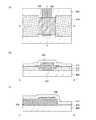
図2は本発明の一態様であるトランジスタの上面図および断面図である。図2(A)に示した一点鎖線A−Bおよび一点鎖線C−Dにおける断面は、それぞれ図2(B)に示すA−B断面および図2(C)に示すC−D断面に対応する。なお、図2(A)では、簡単のため保護絶縁膜218およびゲート絶縁膜212を省略して示す。2A to 2C are a top view and cross-sectional views of a transistor which is one embodiment of the present invention. Cross sections taken along one-dot chain line AB and one-dot chain line CD shown in FIG. 2A correspond to the AB cross section shown in FIG. 2B and the CD cross section shown in FIG. 2C, respectively. . Note that in FIG. 2A, the protective
以下に、図2(B)に示すA−B断面について詳細に説明する。Below, the AB cross section shown to FIG. 2 (B) is demonstrated in detail.
A−B断面は、基板200と、基板200上の第1のゲート電極204と、第1のゲート電極204上の第1のゲート電極204よりも上面形状の小さい第2のゲート電極205と、第1のゲート電極204および第2のゲート電極205を覆うゲート絶縁膜212と、ゲート絶縁膜212上の一対の電極216と、ゲート絶縁膜212上にあり、一部が一対の電極216と接し、かつ少なくとも一部が第2のゲート電極205と重畳する半導体膜206と、ゲート絶縁膜212、半導体膜206および一対の電極216を覆う保護絶縁膜218と、を有するトランジスタの断面である。なお、基板上に下地絶縁膜を設けても構わない。The A-B cross section includes a
第1のゲート電極204および第2のゲート電極205は、幅および高さを以下のように選択する。具体的には、第1のゲート電極204および第2のゲート電極205を用い、三次元形状のチャネル領域を形成することにより、一対の電極216間距離である見かけ上のチャネル長Lに対して、チャネル長L’を3倍以上、好ましくは5倍以上、さらに好ましくは10倍以上の長さとなるように幅および高さを選択すればよい。前述の範囲を満たすために、第2のゲート電極205の断面形状において、側面を形成する辺の長さの和が上面を形成する辺の長さの2倍以上としてもよい。The width and height of the
なお、基板200、第1のゲート電極204、第2のゲート電極205、ゲート絶縁膜212、一対の電極216および保護絶縁膜218は、それぞれ実施の形態1で示す基板100、第1のゲート電極104、第2のゲート電極105、ゲート絶縁膜112、一対の電極116および保護絶縁膜118を参照する。Note that the
第1のゲート電極204および第2のゲート電極205を利用し、三次元形状のチャネル領域を形成することにより、上面図で見る一対の電極216間距離である見かけ上のチャネル長Lに対して、チャネル長L’を3倍以上、好ましくは5倍以上、さらに好ましくは10倍以上の長さとすることができる。そのため、トランジスタを縮小しても短チャネル効果の影響を低減して半導体装置の集積度を高めることが可能となる。また、コストが低く、歩留まりの高い半導体装置を提供することができる。By using the
本実施の形態に示すトランジスタを作製する方法を例示する。A method for manufacturing the transistor described in this embodiment will be described.
まず、基板200上に第1のゲート電極204を形成し、次に第1のゲート電極204上に第1のゲート電極204よりも上面形状の小さい第2のゲート電極205を形成し、次に第1のゲート電極204および第2のゲート電極205を覆うゲート絶縁膜212を形成し、次にゲート絶縁膜212上に一対の電極216を形成し、次にゲート絶縁膜212上にあり、一部が一対の電極216と接し、かつ少なくとも一部が第2のゲート電極205と重畳する半導体膜206を形成し、次にゲート絶縁膜212、半導体膜206および一対の電極216を覆う保護絶縁膜218を形成する。First, the
なお、一対の電極216、第1のゲート電極204および第2のゲート電極205に対して、逆スパッタリング処理などのプラズマ処理を行い、上端部の角をとって曲面形状としても構わない。Note that plasma treatment such as reverse sputtering treatment may be performed on the pair of
本実施の形態は、他の実施の形態と適宜組み合わせて用いることができる。This embodiment can be combined with any of the other embodiments as appropriate.
(実施の形態3)
本実施の形態では、実施の形態1および実施の形態2に示したトランジスタとは異なる構造のトランジスタについて図3を用いて説明する。(Embodiment 3)
In this embodiment, a transistor having a structure different from those of the transistors described in
図3は本発明の一態様であるトランジスタの上面図および断面図である。図3(A)に示した一点鎖線A−Bおよび一点鎖線C−Dにおける断面は、それぞれ図3(B)に示すA−B断面および図3(C)に示すC−D断面に対応する。なお、図3(A)では、簡単のため保護絶縁膜318およびゲート絶縁膜312を省略して示す。3A to 3C are a top view and cross-sectional views of a transistor which is one embodiment of the present invention. Cross sections taken along one-dot chain line AB and one-dot chain line CD shown in FIG. 3A correspond to the AB cross section shown in FIG. 3B and the CD cross section shown in FIG. 3C, respectively. . Note that in FIG. 3A, the protective
以下に、図3(B)に示すA−B断面について詳細に説明する。Below, the AB cross section shown to FIG. 3 (B) is demonstrated in detail.
A−B断面は、基板300と、基板300上のゲート電極305と、ゲート電極305を覆うゲート絶縁膜312と、ゲート絶縁膜312上にあり、少なくとも一部がゲート電極305と重畳する半導体膜306と、半導体膜306上にあり半導体膜306と一部が接する一対の電極316と、ゲート絶縁膜312、半導体膜306および一対の電極316を覆う保護絶縁膜318と、を有するトランジスタの断面である。なお、基板上に下地絶縁膜を設けても構わない。The A-B cross section is the
ゲート電極305は、幅および高さを以下のように選択する。具体的には、ゲート電極305を用い、三次元形状のチャネル領域を形成することにより、一対の電極316間距離である見かけ上のチャネル長Lに対して、チャネル長L’を3倍以上、好ましくは5倍以上、さらに好ましくは10倍以上の長さとなるように幅および高さを選択すればよい。前述の範囲を満たすために、ゲート電極305の断面形状において、側面を形成する辺の長さの和が上面を形成する辺の長さの2倍以上としてもよい。The
なお、基板300、ゲート電極305、ゲート絶縁膜312、一対の電極316および保護絶縁膜318は、それぞれ実施の形態1で示す基板100、第2のゲート電極105、ゲート絶縁膜112、一対の電極116および保護絶縁膜118を参照する。Note that the
ここで、基板上に下地絶縁膜を設ける場合、水素、窒素、ホウ素またはリンなどの半導体膜306中でキャリアを生成する不純物を放出する絶縁膜を設けると好ましい。このような構造とすることで、例えば加熱処理などによって下地絶縁膜から不純物を放出し、半導体膜306のゲート電極305と重畳しない領域にLDD(Lightly Doped Drain)領域を設けることができる。LDD領域を設けることによって、ホットキャリア劣化などのトランジスタの劣化を抑制し、信頼性の高いトランジスタを作製することができる。Here, in the case where the base insulating film is provided over the substrate, it is preferable to provide an insulating film that releases impurities that generate carriers in the
または、半導体膜306において、ゲート電極305と重畳しない領域に対し、プラズマ処理、イオンドーピング処理、イオン注入処理などの低抵抗化処理を行っても構わない。低抵抗化処理によって、半導体膜306にLDD領域を設けることができる。Alternatively, resistance reduction treatment such as plasma treatment, ion doping treatment, or ion implantation treatment may be performed on a region of the
ゲート電極305を利用し、三次元形状のチャネル領域を形成することにより、上面図で見る一対の電極316間距離である見かけ上のチャネル長Lに対して、チャネル長L’を3倍以上、好ましくは5倍以上、さらに好ましくは10倍以上の長さとすることができる。そのため、トランジスタを縮小しても短チャネル効果の影響を低減して半導体装置の集積度を高めることが可能となる。また、コストが低く、歩留まりの高い半導体装置を提供することができる。By using the
本実施の形態に示すトランジスタを作製する方法を例示する。A method for manufacturing the transistor described in this embodiment will be described.
まず、基板300上にゲート電極305を形成し、次にゲート電極305を覆うゲート絶縁膜312を形成し、次にゲート絶縁膜312上にあり、少なくとも一部がゲート電極305と重畳する半導体膜306を形成し、次に半導体膜306上にあり半導体膜306と一部が接する一対の電極316を形成し、次にゲート絶縁膜312、半導体膜306および一対の電極316を覆う保護絶縁膜318を形成する。First, the
なお、ゲート電極305に対して、逆スパッタリング処理などのプラズマ処理を行い、上端部の角をとって曲面形状としても構わない。Note that plasma treatment such as reverse sputtering treatment may be performed on the
本実施の形態は、他の実施の形態と適宜組み合わせて用いることができる。This embodiment can be combined with any of the other embodiments as appropriate.
(実施の形態4)
本実施の形態では、実施の形態1乃至実施の形態3に示したトランジスタとは異なる構造のトランジスタについて図4を用いて説明する。(Embodiment 4)
In this embodiment, a transistor having a structure different from those of the transistors described in
図4は本発明の一態様であるトランジスタの上面図および断面図である。図4(A)に示した一点鎖線A−Bおよび一点鎖線C−Dにおける断面は、それぞれ図4(B)に示すA−B断面および図4(C)に示すC−D断面に対応する。なお、図4(A)では、簡単のため保護絶縁膜418およびゲート絶縁膜412を省略して示す。4A to 4C are a top view and cross-sectional views of a transistor which is one embodiment of the present invention. Cross sections taken along one-dot chain line AB and one-dot chain line CD shown in FIG. 4A correspond to the AB cross section shown in FIG. 4B and the CD cross section shown in FIG. 4C, respectively. . Note that in FIG. 4A, the protective
以下に、図4(B)に示すA−B断面について詳細に説明する。Below, the AB cross section shown to FIG. 4 (B) is demonstrated in detail.
A−B断面は、基板400と、基板400上のゲート電極405と、ゲート電極405を覆うゲート絶縁膜412と、ゲート絶縁膜412上の一対の電極416と、ゲート絶縁膜412上にあり、一部が一対の電極416と接し、かつ少なくとも一部がゲート電極405と重畳する半導体膜406と、ゲート絶縁膜412、半導体膜406および一対の電極416を覆う保護絶縁膜418と、を有するトランジスタの断面である。なお、基板上に下地絶縁膜を設けても構わない。The A-B cross section is on the
ゲート電極405は、幅および高さを以下のように選択する。具体的には、ゲート電極405を用い、三次元形状のチャネル領域を形成することにより、一対の電極416間距離である見かけ上のチャネル長Lに対して、チャネル長L’を3倍以上、好ましくは5倍以上、さらに好ましくは10倍以上の長さとなるように幅および高さを選択すればよい。前述の範囲を満たすために、ゲート電極405の断面形状において、側面を形成する辺の長さの和が上面を形成する辺の長さの2倍以上としてもよい。The
なお、基板400、ゲート電極405、ゲート絶縁膜412、一対の電極416および保護絶縁膜418は、それぞれ実施の形態1で示す基板100、第2のゲート電極105、ゲート絶縁膜112、一対の電極116および保護絶縁膜118を参照する。Note that the
ここで、基板上に下地絶縁膜を設ける場合、水素、窒素、ホウ素またはリンなどの半導体膜406中でキャリアを生成する不純物を放出する絶縁膜を設けると好ましい。このような構造とすることで、例えば加熱処理などによって下地絶縁膜から不純物を放出し、半導体膜406のゲート電極405と重畳しない領域にLDD領域を設けることができる。LDD領域を設けることによって、ホットキャリア劣化などのトランジスタの劣化を抑制し、信頼性の高いトランジスタを作製することができる。Here, in the case where a base insulating film is provided over the substrate, it is preferable to provide an insulating film that releases impurities that generate carriers in the
または、半導体膜406において、ゲート電極405と重畳しない領域に対し、プラズマ処理、イオンドーピング処理、イオン注入処理などの低抵抗化処理を行っても構わない。低抵抗化処理によって、半導体膜406にLDD領域を設けることができる。Alternatively, low resistance treatment such as plasma treatment, ion doping treatment, or ion implantation treatment may be performed on a region of the
ゲート電極405を利用し、三次元形状のチャネル領域を形成することにより、上面図で見る一対の電極416間距離である見かけ上のチャネル長Lに対して、チャネル長L’を3倍以上、好ましくは5倍以上、さらに好ましくは10倍以上の長さとすることができる。そのため、トランジスタを縮小しても短チャネル効果の影響を低減して半導体装置の集積度を高めることが可能となる。また、コストが低く、歩留まりの高い半導体装置を提供することができる。By using the
本実施の形態に示すトランジスタを作製する方法を例示する。A method for manufacturing the transistor described in this embodiment will be described.
まず、基板400上にゲート電極405を形成し、次にゲート電極405を覆うゲート絶縁膜412を形成し、次にゲート絶縁膜412上に一対の電極416を形成し、次にゲート絶縁膜412上にあり、一部が一対の電極416と接し、かつ少なくとも一部がゲート電極405と重畳する半導体膜406を形成し、次にゲート絶縁膜412、半導体膜406および一対の電極416を覆う保護絶縁膜418を形成する。First, the
なお、一対の電極416およびゲート電極405に対して、逆スパッタリング処理などのプラズマ処理を行い、上端部の角をとって曲面形状としても構わない。Note that plasma treatment such as reverse sputtering treatment may be performed on the pair of
本実施の形態は、他の実施の形態と適宜組み合わせて用いることができる。This embodiment can be combined with any of the other embodiments as appropriate.
(実施の形態5)
本実施の形態では、実施の形態1乃至実施の形態4に示したトランジスタとは異なる構造のトランジスタについて図5を用いて説明する。(Embodiment 5)
In this embodiment, a transistor having a structure different from those of the transistors described in
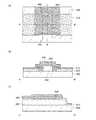
図5は本発明の一態様であるトランジスタの上面図および断面図である。図5(A)に示した一点鎖線A−Bおよび一点鎖線C−Dにおける断面は、それぞれ図5(B)に示すA−B断面および図5(C)に示すC−D断面に対応する。なお、図5(A)では、簡単のためゲート絶縁膜512を省略して示す。5A to 5C are a top view and cross-sectional views of a transistor which is one embodiment of the present invention. Cross sections taken along one-dot chain line AB and one-dot chain line CD shown in FIG. 5A correspond to the AB cross section shown in FIG. 5B and the CD cross section shown in FIG. 5C, respectively. . Note that in FIG. 5A, the
以下に、図5(B)に示すA−B断面について詳細に説明する。Below, the AB cross section shown to FIG. 5 (B) is demonstrated in detail.
A−B断面は、基板500と、基板500上の構造物502と、少なくとも一部が構造物502と重畳する半導体膜506と、半導体膜506上にあり半導体膜506と一部が接する一対の電極516と、半導体膜506を覆うゲート絶縁膜512と、ゲート絶縁膜512を介して半導体膜506に重畳するゲート電極505と、を有するトランジスタの断面である。なお、基板上に下地絶縁膜を設けても構わない。The A-B cross section is a pair of a
構造物502は、幅および高さを以下のように選択する。具体的には、構造物502を用い、三次元形状のチャネル領域を形成することにより、一対の電極516間距離である見かけ上のチャネル長Lに対して、チャネル長L’を3倍以上、好ましくは5倍以上、さらに好ましくは10倍以上の長さとなるように幅および高さを選択すればよい。前述の範囲を満たすために、構造物502の断面形状において、側面を形成する辺の長さの和が上面を形成する辺の長さの2倍以上としてもよい。The
図5では、ゲート電極505と一対の電極516とが重畳するように記載しているが、これに限定されるものではない、例えば、ゲート電極505と一対の電極516とが重畳しなくても構わない。その場合、半導体膜506のゲート電極505と重畳しない領域に低抵抗化処理を行い、LDD領域を設けても構わない。LDD領域を設けることによってホットキャリア劣化などのトランジスタの劣化が抑制され、信頼性の高いトランジスタを作製することができる。また、一対の電極516とゲート電極505とで形成される寄生容量を低減することができるため、トランジスタの動作速度を速くすることができる。In FIG. 5, the
構造物502は、後の熱処理に耐える材料であればよく、例えば、酸化シリコン、酸化窒化シリコン、窒化酸化シリコン、窒化シリコン、酸化アルミニウム、酸化窒化アルミニウム、窒化酸化アルミニウム、窒化アルミニウムなどの無機化合物またはポリイミドなどの有機化合物を用いればよい。The
半導体膜506が酸化物半導体膜であるとき、構造物502として、加熱処理により酸素を放出する膜を用いると好ましい。また、基板500上に下地絶縁膜として、加熱処理により酸素を放出する膜を設けても構わない。構造物502および下地絶縁膜として、加熱処理により酸素を放出する膜を設けることで、半導体膜506と構造物502との界面の界面準位密度、または半導体膜506と下地絶縁膜との界面の界面準位密度、ならびに酸化物半導体膜である半導体膜506の酸素欠損を低減し、酸化物半導体膜である半導体膜506と構造物502または下地絶縁膜との界面におけるキャリア捕獲の影響を小さくすることができる。When the
または、基板上に下地絶縁膜を設ける場合、水素、窒素、ホウ素またはリンなどの半導体膜506中でキャリアを生成する不純物を放出する絶縁膜を設けると好ましい。このような構造とすることで、例えば加熱処理などによって下地絶縁膜から不純物を放出し、半導体膜506の構造物502と重畳しない領域にLDD領域を設けることができる。LDD領域を設けることによって、ホットキャリア劣化などのトランジスタの劣化を抑制し、信頼性の高いトランジスタを作製することができる。また、構造物502を積層構造とし、下地絶縁膜と接する側に水素、窒素、ホウ素またはリンなどをほとんど透過しない膜を設け、ゲート絶縁膜512側に加熱処理により酸素を放出する膜を設けても構わない。構造物502に加熱処理により酸素を放出する膜を設けることで、形成されるチャネル領域において酸素欠損を低減でき、また、構造物502と半導体膜506との界面準位密度を低減することができる。そのため、トランジスタの電気特性および信頼性を向上させることができる。Alternatively, in the case where a base insulating film is provided over the substrate, it is preferable to provide an insulating film that releases impurities that generate carriers in the
または、半導体膜506において、構造物502と重畳しない領域に対し、プラズマ処理、イオンドーピング処理、イオン注入処理などの低抵抗化処理を行っても構わない。低抵抗化処理によって、半導体膜506にLDD領域を設けることができる。Alternatively, resistance reduction treatment such as plasma treatment, ion doping treatment, or ion implantation treatment may be performed on a region of the
なお、基板500、ゲート電極505、ゲート絶縁膜512および一対の電極516は、それぞれ実施の形態1で示す基板100、第2のゲート電極105、ゲート絶縁膜112および一対の電極116を参照する。Note that the
構造物502を利用し、三次元形状のチャネル領域を形成することにより、上面図で見る一対の電極516間距離である見かけ上のチャネル長Lに対して、チャネル長L’を3倍以上、好ましくは5倍以上、さらに好ましくは10倍以上の長さとすることができる。そのため、トランジスタを縮小しても短チャネル効果の影響を低減して半導体装置の集積度を高めることが可能となる。また、コストが低く、歩留まりの高い半導体装置を提供することができる。By using the
本実施の形態に示すトランジスタを作製する方法を例示する。A method for manufacturing the transistor described in this embodiment will be described.
まず、基板500上に構造物502を形成し、次に少なくとも一部が構造物502と重畳する半導体膜506を形成し、次に半導体膜506上にあり半導体膜506と一部が接する一対の電極516を形成し、次に半導体膜506を覆うゲート絶縁膜512を形成し、次にゲート絶縁膜512を介して半導体膜506に重畳するゲート電極505を形成する。First, the
なお、一対の電極516および構造物502に対して、逆スパッタリング処理などのプラズマ処理を行い、上端部の角をとって曲面形状としても構わない。Note that plasma treatment such as reverse sputtering treatment may be performed on the pair of
本実施の形態は、他の実施の形態と適宜組み合わせて用いることができる。This embodiment can be combined with any of the other embodiments as appropriate.
(実施の形態6)
本実施の形態では、実施の形態1乃至実施の形態5に示したトランジスタとは異なる構造のトランジスタについて図6を用いて説明する。(Embodiment 6)
In this embodiment, a transistor having a structure different from those of the transistors described in
図6は本発明の一態様であるトランジスタの上面図および断面図である。図6(A)に示した一点鎖線A−Bおよび一点鎖線C−Dにおける断面は、それぞれ図6(B)に示すA−B断面および図6(C)に示すC−D断面に対応する。6A to 6C are a top view and cross-sectional views of a transistor which is one embodiment of the present invention. The cross sections along the alternate long and short dash line AB and the alternate long and short dash line CD shown in FIG. 6A correspond to the AB cross section shown in FIG. 6B and the CD cross section shown in FIG. 6C, respectively. .
以下に、図6(B)に示すA−B断面について詳細に説明する。Below, the AB cross section shown to FIG. 6 (B) is demonstrated in detail.
A−B断面は、基板600と、基板600上の構造物602と、少なくとも一部が構造物602と重畳する半導体膜606と、半導体膜606下にあり半導体膜606と一部が接する一対の電極616と、半導体膜606を覆うゲート絶縁膜612と、ゲート絶縁膜612を介して半導体膜606に重畳するゲート電極605と、を有するトランジスタの断面である。なお、基板上に下地絶縁膜を設けても構わない。The A-B cross section is a pair of a
構造物602は、幅および高さを最適化する必要がある。具体的には、構造物602を用い、三次元形状のチャネル領域を形成することにより、一対の電極616間距離である見かけ上のチャネル長Lに対して、チャネル長L’を3倍以上、好ましくは5倍以上、さらに好ましくは10倍以上の長さとなるように幅および高さを選択すればよい。前述の範囲を満たすために、構造物602の断面形状において、側面を形成する辺の長さの和が上面を形成する辺の長さの2倍以上としてもよい。The
図6では、ゲート電極605と一対の電極616とが重畳するように記載しているが、これに限定されるものではない、例えば、ゲート電極605と一対の電極616とが重畳しなくても構わない。その場合、半導体膜606のゲート電極605と重畳しない領域に低抵抗化処理を行い、LDD領域を設けても構わない。LDD領域を設けることによってホットキャリア劣化などのトランジスタの劣化が抑制され、信頼性の高いトランジスタを作製することができる。また、一対の電極616とゲート電極605とで形成される寄生容量を低減することができるため、トランジスタの動作速度を速くすることができる。In FIG. 6, the
構造物602は、実施の形態5で示した構造物502と同様の材料を用いて形成すればよい。The
半導体膜606が酸化物半導体膜であるとき、構造物602は、加熱処理により酸素を放出する膜を用いると好ましい。また、基板600上に下地絶縁膜として、加熱処理により酸素を放出する膜を設けても構わない。When the
または、基板上に下地絶縁膜を設ける場合、水素、窒素、ホウ素またはリンなどの半導体膜606中でキャリアを生成する不純物を放出する絶縁膜を設けると好ましい。このような構造とすることで、例えば加熱処理などによって下地絶縁膜から不純物を放出し、半導体膜606の構造物602と重畳しない領域にLDD領域を設けることができる。LDD領域を設けることによって、ホットキャリア劣化などのトランジスタの劣化を抑制し、信頼性の高いトランジスタを作製することができる。また、構造物602を積層構造とし、下地絶縁膜と接する側に水素、窒素、ホウ素またはリンなどをほとんど透過しない膜を設け、ゲート絶縁膜612側に加熱処理により酸素を放出する膜を設けても構わない。構造物602に加熱処理により酸素を放出する膜を設けることで、形成されるチャネル領域において酸素欠損を低減でき、また、構造物602と半導体膜606との界面準位密度を低減することができる。そのため、トランジスタの電気特性および信頼性を向上させることができる。Alternatively, in the case where a base insulating film is provided over the substrate, it is preferable to provide an insulating film that releases impurities that generate carriers in the
または、半導体膜606において、構造物602と重畳しない領域に対し、プラズマ処理、イオンドーピング処理、イオン注入処理などの低抵抗化処理を行っても構わない。低抵抗化処理によって、半導体膜606にLDD領域を設けることができる。Alternatively, resistance reduction treatment such as plasma treatment, ion doping treatment, or ion implantation treatment may be performed on a region of the
なお、基板600、ゲート電極605、ゲート絶縁膜612および一対の電極616は、それぞれ実施の形態1で示す基板100、第2のゲート電極105、ゲート絶縁膜112および一対の電極116を参照する。Note that for the
構造物602を利用し、三次元形状のチャネル領域を形成することにより、上面図で見る一対の電極616間距離である見かけ上のチャネル長Lに対して、チャネル長L’を3倍以上、好ましくは5倍以上、さらに好ましくは10倍以上の長さとすることができる。そのため、トランジスタを縮小しても短チャネル効果の影響を低減して半導体装置の集積度を高めることが可能となる。また、コストが低く、歩留まりの高い半導体装置を提供することができる。By using the
本実施の形態に示すトランジスタを作製する方法を例示する。A method for manufacturing the transistor described in this embodiment will be described.
まずは、基板600上に構造物602を形成し、次に少なくとも一部が構造物602と重畳する半導体膜606を形成し、次に半導体膜606下にあり半導体膜606と一部が接する一対の電極616を形成し、次に半導体膜606を覆うゲート絶縁膜612を形成し、次にゲート絶縁膜612を介して半導体膜606に重畳するゲート電極605を形成する。First, the
なお、一対の電極616および構造物602に対して、逆スパッタリング処理などのプラズマ処理を行い、上端部の角をとって曲面形状としても構わない。Note that plasma treatment such as reverse sputtering treatment may be performed on the pair of
本実施の形態は、他の実施の形態と適宜組み合わせて用いることができる。This embodiment can be combined with any of the other embodiments as appropriate.
(実施の形態7)
本実施の形態では、実施の形態1乃至実施の形態6に示したトランジスタに適用可能なゲート電極または構造物の断面形状について、図7を用いて説明する。(Embodiment 7)
In this embodiment, a cross-sectional shape of a gate electrode or a structure which can be applied to the transistor described in any of
図7(A)は、実施の形態1および実施の形態2において、上面図で見る一対の電極間距離である見かけ上のチャネル長Lに対して、さらにチャネル長L’を長くするために基板700上に設けられた第1のゲート電極704、第2のゲート電極705a、第2のゲート電極705bおよび第2のゲート電極705cを示す断面形状である。ここで、基板700、第1のゲート電極704、ならびに第2のゲート電極705a、第2のゲート電極705bおよび第2のゲート電極705cは、それぞれ実施の形態1および実施の形態2における基板100および基板200、第1のゲート電極104および第1のゲート電極204、ならびに第2のゲート電極105および第2のゲート電極205を参照する。FIG. 7A shows a substrate for further increasing the channel length L ′ with respect to the apparent channel length L which is the distance between a pair of electrodes seen in the top view in the first and second embodiments. A cross-sectional shape of the
第2のゲート電極705a、第2のゲート電極705bおよび第2のゲート電極705cを設けることで、実施の形態1および実施の形態2で示したトランジスタと比べ、さらに、その後形成する半導体膜が形成するチャネル長L’を長くすることができる。また、一つ一つの第2のゲート電極の厚さを薄くできるため、後に形成するゲート絶縁膜および半導体膜などの被覆性を高めることができる。なお、第2のゲート電極の形状は、第2のゲート電極705a、第2のゲート電極705bおよび第2のゲート電極705cに限定されるものではない。例えば、第2のゲート電極705aおよび第2のゲート電極705bのみとしても構わないし、第2のゲート電極を四以上設けても構わない。By providing the
図7(B)は、実施の形態3および実施の形態4において、上面図で見る一対の電極間距離である見かけ上のチャネル長Lに対して、さらにチャネル長L’を長くするために基板700上に設けられたゲート電極705d、ゲート電極705eおよびゲート電極705fを示す断面形状である。また、一つ一つのゲート電極の厚さを薄くできるため、後に形成するゲート絶縁膜および半導体膜などの被覆性を高めることができる。ゲート電極705d、ゲート電極705eおよびゲート電極705fは、図示しないが電気的に接続されている。ここで、ゲート電極705d、ゲート電極705eおよびゲート電極705fは、実施の形態3および実施の形態4におけるゲート電極305およびゲート電極405を参照する。FIG. 7B shows a substrate in Embodiment 3 and Embodiment 4 in order to further increase the channel length L ′ with respect to the apparent channel length L which is the distance between a pair of electrodes seen in the top view. The
ゲート電極705d、ゲート電極705eおよびゲート電極705fを設けることで、実施の形態3および実施の形態4で示したトランジスタと比べ、さらに、その後形成する半導体膜が形成するチャネル長L’を長くすることができる。なお、ゲート電極の形状は、ゲート電極705d、ゲート電極705eおよびゲート電極705fに限定されるものではない。例えば、ゲート電極705dおよびゲート電極705eのみとしても構わないし、ゲート電極を四以上設けても構わない。By providing the
図7(C)は、実施の形態5および実施の形態6において、上面図で見る一対の電極間距離である見かけ上のチャネル長Lに対して、さらにチャネル長L’を長くするために基板700上に設けられた構造物702a、構造物702bおよび構造物702cを示す断面形状である。また、一つ一つの構造物の厚さを薄くできるため、後に形成するゲート絶縁膜および半導体膜などの被覆性を高めることができる。ここで、構造物702a、構造物702bおよび構造物702cは、それぞれ実施の形態5および実施の形態6における構造物502および構造物602を参照する。FIG. 7C shows a substrate for further increasing the channel length L ′ with respect to the apparent channel length L which is the distance between the pair of electrodes seen in the top view in the fifth and sixth embodiments. The cross-sectional shape of the
構造物702a、構造物702bおよび構造物702cを設けることで、実施の形態5および実施の形態6で示したトランジスタと比べ、さらに、その後形成する半導体膜が形成するチャネル長L’を長くすることができる。なお、構造物の形状は、構造物702a、構造物702bおよび構造物702cに限定されるものではない。例えば、構造物702aおよび構造物702bのみとしても構わないし、構造物を四以上設けても構わない。By providing the
本実施の形態により、実施の形態1乃至実施の形態6で示したトランジスタよりもさらにチャネル長L’を長くすることが可能となる。そのため、さらにトランジスタを縮小しても短チャネル効果の影響を低減して半導体装置の集積度を高めることが可能となる。また、コストが低く、歩留まりの高い半導体装置を提供することができる。According to this embodiment mode, the channel length L ′ can be further increased as compared with the transistors described in
(実施の形態8)
本実施の形態では、実施の形態1乃至実施の形態7のいずれかに示したトランジスタを用いて、半導体記憶装置を作製する例について説明する。(Embodiment 8)
In this embodiment, an example in which a semiconductor memory device is manufactured using any of the transistors described in any of
揮発性半導体記憶装置の代表的な例としては、記憶素子を構成するトランジスタを選択してキャパシタに電荷を蓄積することで、情報を記憶するDRAM、フリップフロップなどの回路を用いて記憶内容を保持するSRAM(Static Random Access Memory)がある。As a typical example of a volatile semiconductor memory device, the memory contents are held using a circuit such as a DRAM or flip-flop for storing information by selecting a transistor constituting the memory element and accumulating electric charge in the capacitor. SRAM (Static Random Access Memory).
不揮発性半導体記憶装置の代表例としては、トランジスタのゲート電極とチャネル形成領域との間にフローティングゲートを有し、当該フローティングゲートに電荷を保持することで記憶を行うフラッシュメモリがある。As a typical example of a nonvolatile semiconductor memory device, there is a flash memory which has a floating gate between a gate electrode of a transistor and a channel formation region and stores data by holding electric charge in the floating gate.
上述した半導体記憶装置に含まれるトランジスタの一部に実施の形態1乃至実施の形態7のいずれかで示したトランジスタを適用することができる。The transistor described in any of
まずは、実施の形態1乃至実施の形態7のいずれかで示したトランジスタを適用した半導体記憶装置を構成するメモリセルについて図8を用いて説明する。First, a memory cell included in a semiconductor memory device to which the transistor described in any of
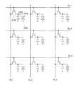
メモリセルは、ビット線BLと、ワード線WLと、センスアンプSAmpと、トランジスタTrと、キャパシタCと、を有する(図8(A)参照。)。The memory cell includes a bit line BL, a word line WL, a sense amplifier SAmp, a transistor Tr, and a capacitor C (see FIG. 8A).
ここで、図8(A)に示すメモリセルを有する半導体記憶装置の集積度を高めていくと、トランジスタTrもそれに伴いサイズを縮小していく必要が生じる。ところが、単にトランジスタTrのサイズを縮小していくと、ある程度以下のサイズとしたとき、トランジスタTrにおける短チャネル効果が無視できなくなる。これは、短チャネル効果によりパンチスルー電流が流れやすくなり、トランジスタがスイッチング素子として機能しなくなるためである。Here, when the degree of integration of the semiconductor memory device including the memory cell illustrated in FIG. 8A is increased, the size of the transistor Tr needs to be reduced accordingly. However, if the size of the transistor Tr is simply reduced, the short channel effect in the transistor Tr cannot be ignored when the size is reduced to some extent. This is because the punch-through current easily flows due to the short channel effect, and the transistor does not function as a switching element.
本発明の一形態をトランジスタTrに適用することで、トランジスタTrの占有面積は小さくでき、かつチャネル長を長くすることができる。そのため、半導体記憶装置の集積度を高めることが可能となる。By applying one embodiment of the present invention to the transistor Tr, the area occupied by the transistor Tr can be reduced and the channel length can be increased. As a result, the degree of integration of the semiconductor memory device can be increased.
なお、キャパシタに保持された電位の時間変化は、トランジスタTrのオフ電流によって図8(B)に示すように徐々に低減していくことが知られている。当初V0からV1まで充電された電位は、時間が経過するとdata1を読み出す限界点であるVAまで低減する。この期間を保持期間T_1とする。即ち、2値メモリセルの場合、保持期間T_1の間にリフレッシュをする必要がある。It is known that the time change of the potential held in the capacitor is gradually reduced as shown in FIG. 8B by the off-state current of the transistor Tr. The potential initially charged from V0 to V1 is reduced to VA, which is a limit point for reading data1 over time. This period is a holding period T_1. That is, in the case of a binary memory cell, it is necessary to refresh during the holding period T_1.
ここで、トランジスタTrのチャネル領域を形成する半導体膜に酸化物半導体膜を用いると、酸化物半導体膜を用いたトランジスタはオフ電流が小さくできるため、保持期間T_1を長くすることができる。即ち、リフレッシュの頻度を少なくすることが可能となるため、消費電力を低減することができる。例えば、オフ電流が1×10⁻²¹A以下、好ましくは1×10⁻²⁴A以下となった酸化物半導体膜を用いたトランジスタでメモリセルを構成すると、電力を供給せずに数日間〜数十年間に渡ってデータを保持することが可能となる。Here, when an oxide semiconductor film is used for the semiconductor film forming the channel region of the transistor Tr, the off-state current of the transistor including the oxide semiconductor film can be reduced; thus, the holding period T_1 can be extended. That is, since the frequency of refresh can be reduced, power consumption can be reduced. For example, when a memory cell is formed using a transistor including an oxide semiconductor film with an off-state current of 1 × 10⁻²¹ A or less, preferably 1 × 10⁻²⁴ A or less, several days to several days without supplying power Data can be retained for 10 years.
図8(C)および図8(D)に、それぞれ実施の形態1および実施の形態5で示したトランジスタで構成したメモリセルの断面構造を示す。なお、図8(C)および図8(D)には、実施の形態1乃至実施の形態7で示したいずれのトランジスタも適用することができるが、簡単のため上記トランジスタのみを示す。8C and 8D show cross-sectional structures of memory cells formed using the transistors described in
図8(C)は、基板100上に設けられた半導体膜106を有するトランジスタ801およびキャパシタ802の断面構造である。なお、キャパシタ802は、第1のゲート電極104と同一層かつ同一材料の導電膜と、第2のゲート電極105と同一層かつ同一材料の導電膜と、で構成される第1の容量電極、一対の電極116の一方と接続する第2の容量電極およびゲート絶縁膜112と同一層かつ同一材料である誘電体層を有する。トランジスタ801のみならず、キャパシタ802に対しても本発明の一態様を適用することによって、三次元のキャパシタ形状を得ることができるため、キャパシタの占有面積も縮小することができる。なお、保護絶縁膜118は必ずしも設けなくてよい。FIG. 8C illustrates a cross-sectional structure of the
図8(D)は、基板500上に設けられた半導体膜506を有するトランジスタ811およびキャパシタ812の断面構造である。なお、キャパシタ812は、ゲート電極505と同一層かつ同一材料である第1の容量電極、一対の電極516の一方と接続する第2の容量電極およびゲート絶縁膜512と同一層かつ同一材料である誘電体層を有する。トランジスタ811のみならず、キャパシタ812に対しても本発明の一態様を適用することによって、三次元のキャパシタ形状を得ることができるため、キャパシタの占有面積も縮小することができる。FIG. 8D illustrates a cross-sectional structure of the
以上のように、キャパシタに対して本発明の一態様を適用することができる。図示しないが、他の形態に上記したキャパシタの構造を適用しても構わない。As described above, one embodiment of the present invention can be applied to a capacitor. Although not shown, the capacitor structure described above may be applied to other forms.
以上のように、本発明の一態様によって、集積度を高めても短チャネル効果が低減され、長期間の信頼性が高く、かつ消費電力の小さい半導体記憶装置を得ることができる。As described above, according to one embodiment of the present invention, a short-channel effect is reduced even when the degree of integration is increased, and a semiconductor memory device with high long-term reliability and low power consumption can be obtained.
次に、実施の形態1乃至実施の形態7のいずれかで示したトランジスタを適用した半導体記憶装置について図9を用いて説明する。Next, a semiconductor memory device to which the transistor described in any of
図9(A)は、半導体記憶装置を構成するメモリセルの回路図である。メモリセルは、トランジスタTr_1と、トランジスタTr_1のゲートと接続するゲート線GL_1と、トランジスタTr_1のソースと接続するソース線SL_1と、トランジスタTr_2と、トランジスタTr_2のソースと接続するソース線SL_2と、トランジスタTr_2のドレインと接続するドレイン線DL_2と、キャパシタCと、キャパシタCの一端と接続する容量線CLと、キャパシタCの他端、トランジスタTr_1のドレインおよびトランジスタTr_2のゲートと接続するノードFGと、を有する。FIG. 9A is a circuit diagram of a memory cell included in the semiconductor memory device. The memory cell includes a transistor Tr_1, a gate line GL_1 connected to the gate of the transistor Tr_1, a source line SL_1 connected to the source of the transistor Tr_1, a transistor Tr_2, a source line SL_2 connected to the source of the transistor Tr_2, and a transistor Tr_2. A drain line DL_2 connected to the drain of the capacitor C, a capacitor C, a capacitance line CL connected to one end of the capacitor C, and a node FG connected to the other end of the capacitor C, the drain of the transistor Tr_1, and the gate of the transistor Tr_2. .
図9(A)に示すメモリセルを有する半導体記憶装置も、集積度を高めていくと、トランジスタTr_1およびトランジスタTr_2もそれに伴いサイズを縮小していく必要が生じる。図9(A)に示すメモリセルは、図8(A)に示すメモリセルと比べ、トランジスタの数が多いため、集積度を高めるにはさらにトランジスタサイズの縮小が重要となる。As the degree of integration of the semiconductor memory device including the memory cell illustrated in FIG. 9A also increases, the size of the transistor Tr_1 and the transistor Tr_2 needs to be reduced accordingly. The memory cell illustrated in FIG. 9A has a larger number of transistors than the memory cell illustrated in FIG. 8A. Therefore, in order to increase the degree of integration, it is important to further reduce the transistor size.
本発明の一形態をトランジスタTr_1およびトランジスタTr_2に適用することで、トランジスタTr_1およびトランジスタTr_2の占有面積は小さくでき、かつチャネル長を長くすることができる。そのため、図9(A)に示すメモリセルを有する半導体記憶装置の集積度を高めることが可能となる。By applying one embodiment of the present invention to the transistor Tr_1 and the transistor Tr_2, the area occupied by the transistor Tr_1 and the transistor Tr_2 can be reduced and the channel length can be increased. Therefore, the integration degree of the semiconductor memory device including the memory cell illustrated in FIG. 9A can be increased.
なお、図9(A)に示すメモリセルを有する半導体記憶装置は、ノードFGの電位に応じて、トランジスタTr_2のしきい値が変動することを利用したものである。例えば、図9(B)は容量線CLの電位VCLと、トランジスタTr_2を流れるドレイン電流Ids_2との関係を説明する図である。Note that the semiconductor memory device including the memory cell illustrated in FIG. 9A uses the fact that the threshold value of the transistor Tr_2 varies depending on the potential of the node FG. For example, FIG. 9B illustrates a relationship between the potential VCL of the capacitor line CL and the drain current Ids_2 flowing through the transistor Tr_2.
ここで、ノードFGは、トランジスタTr_1を介して、電位を調整することができる。例えば、ソース線SL_1の電位をVDDとする。このとき、ゲート線GL_1の電位をトランジスタTr_1のしきい値電圧VthにVDDを加えた電位以上とすることで、ノードFGの電位をHIGHにすることができる。また、ゲート線GL_1の電位をトランジスタTr_1のしきい値電圧Vth以下とすることで、ノードFGの電位をLOWにすることができる。Here, the potential of the node FG can be adjusted through the transistor Tr_1. For example, the potential of the source line SL_1 is set to VDD. At this time, the potential of the node FG can be set high by setting the potential of the gate line GL_1 to be equal to or higher than the threshold voltage Vth of the transistor Tr_1 plus VDD. In addition, when the potential of the gate line GL_1 is equal to or lower than the threshold voltage Vth of the transistor Tr_1, the potential of the node FG can be set to LOW.
そのため、FG=LOWで示したVCL−Ids_2カーブと、FG=HIGHで示したVCL−Ids_2カーブのいずれかを得ることができる。即ち、FG=LOWでは、VCL=0VにてIds_2が小さいため、データ0となる。また、FG=HIGHでは、VCL=0VにてIds_2が大きいため、データ1となる。このようにして、データを記憶することができる。Therefore, it is possible to obtain aV CL -Ids_2 curve shown in FG = LOW, one ofV CL -Ids_2 curve shown in FG = HIGH. That is, when FG = LOW, since Ids_2 is small when VCL = 0V, data 0 is obtained. Further, when FG = HIGH,
ここで、トランジスタTr_1として、チャネル領域を形成する半導体膜に酸化物半導体膜を用いたトランジスタを適用すると、該トランジスタはオフ電流を極めて小さくすることができるため、ノードFGに蓄積された電荷がトランジスタTr_1を通して意図せずにリークすることを抑制できる。そのため、長期間に渡ってデータを保持することができる。Here, when a transistor in which an oxide semiconductor film is used as a semiconductor film that forms a channel region is used as the transistor Tr_1, the transistor can reduce off-state current, so that charge accumulated in the node FG can be reduced. Unintentional leakage through Tr_1 can be suppressed. Therefore, data can be held for a long time.
なお、トランジスタTr_2として、チャネル領域を形成する半導体膜に酸化物半導体膜を用いたトランジスタを適用しても構わない。Note that as the transistor Tr_2, a transistor including an oxide semiconductor film as a semiconductor film for forming a channel region may be used.
次に、図9(A)に示したメモリセルにおいて、キャパシタを含まない構成について図10を用いて説明する。Next, a structure in which the memory cell illustrated in FIG. 9A does not include a capacitor is described with reference to FIGS.
図10は、半導体記憶装置を構成するメモリセルの回路図である。メモリセルは、トランジスタTr_1と、トランジスタTr_1のゲートと接続するゲート線GL_1と、トランジスタTr_1のソースと接続するソース線SL_1と、トランジスタTr_2と、トランジスタTr_2のソースと接続するソース線SL_2と、トランジスタTr_2のドレインと接続するドレイン線DL_2と、トランジスタTr_1のドレインと接続するトランジスタTr_2のゲートと、を有する。FIG. 10 is a circuit diagram of a memory cell constituting the semiconductor memory device. The memory cell includes a transistor Tr_1, a gate line GL_1 connected to the gate of the transistor Tr_1, a source line SL_1 connected to the source of the transistor Tr_1, a transistor Tr_2, a source line SL_2 connected to the source of the transistor Tr_2, and a transistor Tr_2. A drain line DL_2 connected to the drain of the transistor Tr_1 and a gate of the transistor Tr_2 connected to the drain of the transistor Tr_1.
なお、トランジスタTr_1のチャネル領域を形成する半導体膜に酸化物半導体膜を用いると、キャパシタを設けなくてもトランジスタTr_1のドレインとトランジスタTr_2のゲートの間に電荷を保持できる。キャパシタを設けない構成であるため、小面積化が可能となり、キャパシタを設けた場合と比べ半導体記憶装置の集積度を高めることができる。Note that when an oxide semiconductor film is used for the semiconductor film forming the channel region of the transistor Tr_1, electric charge can be held between the drain of the transistor Tr_1 and the gate of the transistor Tr_2 without providing a capacitor. Since the capacitor is not provided, the area can be reduced, and the degree of integration of the semiconductor memory device can be increased as compared with the case where the capacitor is provided.
半導体記憶装置の集積度を高めていくと、トランジスタTr_1およびトランジスタTr_2もそれに伴いサイズを縮小していく必要が生じる。キャパシタを設けない構成とすることで、半導体記憶装置に占めるトランジスタの割合が大きくなり、ますますトランジスタサイズの縮小が重要となる。As the degree of integration of the semiconductor memory device increases, it is necessary to reduce the sizes of the transistors Tr_1 and Tr_2 accordingly. By adopting a configuration in which no capacitor is provided, the proportion of transistors in the semiconductor memory device increases, and it is increasingly important to reduce the transistor size.
本発明の一形態をトランジスタTr_1およびトランジスタTr_2に適用することで、トランジスタの占有面積は小さくした際も、チャネル長を長くすることができる。そのため、半導体記憶装置の集積度を高めることが可能となる。By applying one embodiment of the present invention to the transistor Tr_1 and the transistor Tr_2, the channel length can be increased even when the area occupied by the transistor is reduced. As a result, the degree of integration of the semiconductor memory device can be increased.
また、本実施の形態では、配線を4本または5本用いる形態を示したが、これに限定されるものではない。例えば、ソース線SL_1とドレイン線DL_2を共通にする構成としても構わない。Further, in this embodiment mode, an embodiment in which four or five wirings are used is shown, but the present invention is not limited to this. For example, the source line SL_1 and the drain line DL_2 may be shared.
以上のように、本発明の一態様によって、集積度を高めても短チャネル効果が低減され、長期間の信頼性が高く、かつ消費電力の小さい半導体記憶装置を得ることができる。As described above, according to one embodiment of the present invention, a short-channel effect is reduced even when the degree of integration is increased, and a semiconductor memory device with high long-term reliability and low power consumption can be obtained.
本実施の形態は、他の実施の形態と適宜組み合わせて用いることができる。This embodiment can be combined with any of the other embodiments as appropriate.
(実施の形態9)
実施の形態1乃至実施の形態8の少なくともいずれかを一部に適用して、CPU(Central Processing Unit)を構成することができる。(Embodiment 9)
A CPU (Central Processing Unit) can be configured by applying at least one of
図11(A)は、CPUの具体的な構成を示すブロック図である。図11(A)に示すCPUは、基板1190上に、演算回路(ALU:Arithmetic logic unit)1191、ALUコントローラ1192、インストラクションデコーダ1193、インタラプトコントローラ1194、タイミングコントローラ1195、レジスタ1196、レジスタコントローラ1197、バスインターフェース(Bus I/F)1198、書き換え可能なROM1199、およびROMインターフェース(ROM I/F)1189を有している。基板1190は、半導体基板、SOI基板、ガラス基板などを用いる。ROM1199およびROMインターフェース1189は、別チップに設けてもよい。もちろん、図11(A)に示すCPUは、その構成を簡略化して示した一例にすぎず、実際のCPUはその用途によって多種多様な構成を有している。FIG. 11A is a block diagram illustrating a specific configuration of a CPU. 11A includes an arithmetic circuit (ALU) 1191, an
バスインターフェース1198を介してCPUに入力された命令は、インストラクションデコーダ1193に入力され、デコードされた後、ALUコントローラ1192、インタラプトコントローラ1194、レジスタコントローラ1197、タイミングコントローラ1195に入力される。Instructions input to the CPU via the
ALUコントローラ1192、インタラプトコントローラ1194、レジスタコントローラ1197、タイミングコントローラ1195は、デコードされた命令に基づき、各種制御を行なう。具体的にALUコントローラ1192は、ALU1191の動作を制御するための信号を生成する。また、インタラプトコントローラ1194は、CPUのプログラム実行中に、外部の入出力装置や、周辺回路からの割り込み要求を、その優先度やマスク状態から判断し、処理する。レジスタコントローラ1197は、レジスタ1196のアドレスを生成し、CPUの状態に応じてレジスタ1196の読み出しや書き込みを行なう。The
また、タイミングコントローラ1195は、ALU1191、ALUコントローラ1192、インストラクションデコーダ1193、インタラプトコントローラ1194、およびレジスタコントローラ1197の動作のタイミングを制御する信号を生成する。例えばタイミングコントローラ1195は、基準クロック信号CLK1を元に、内部クロック信号CLK2を生成する内部クロック生成部を備えており、クロック信号CLK2を上記各種回路に供給する。In addition, the
図11(A)に示すCPUでは、レジスタ1196に、記憶素子が設けられている。レジスタ1196の記憶素子には、実施の形態8に記載されている記憶素子を用いることができる。In the CPU illustrated in FIG. 11A, the
図11(A)に示すCPUにおいて、レジスタコントローラ1197は、ALU1191からの指示に従い、レジスタ1196における保持動作の選択を行う。すなわち、レジスタ1196が有する記憶素子において、位相反転素子によるデータの保持を行うか、容量素子によるデータの保持を行うかを、選択する。位相反転素子によるデータの保持が選択されている場合、レジスタ1196内の記憶素子への、電源電圧の供給が行われる。容量素子におけるデータの保持が選択されている場合、容量素子へのデータの書き換えが行われ、レジスタ1196内の記憶素子への電源電圧の供給を停止することができる。In the CPU illustrated in FIG. 11A, the
電源停止に関しては、図11(B)または図11(C)に示すように、記憶素子群と、電源電位VDDまたは電源電位VSSの与えられているノード間に、スイッチング素子を設けることにより行うことができる。以下に図11(B)および図11(C)の回路の説明を行う。The power supply is stopped by providing a switching element between the memory element group and the node to which the power supply potential VDD or the power supply potential VSS is applied as shown in FIG. 11B or 11C. Can do. The circuits in FIGS. 11B and 11C will be described below.
図11(B)および図11(C)では、記憶素子への電源電位の供給を制御するスイッチング素子に、酸化物半導体を活性層に用いたトランジスタを含む記憶回路の構成の一例を示す。11B and 11C illustrate an example of a structure of a memory circuit including a transistor in which an oxide semiconductor is used for an active layer as a switching element that controls supply of a power supply potential to the memory element.
図11(B)に示す記憶装置は、スイッチング素子1141と、記憶素子1142を複数有する記憶素子群1143とを有している。具体的に、各記憶素子1142には、実施の形態8に記載されている記憶素子を用いることができる。記憶素子群1143が有する各記憶素子1142には、スイッチング素子1141を介して、ハイレベルの電源電位VDDが供給されている。さらに、記憶素子群1143が有する各記憶素子1142には、信号INの電位と、ローレベルの電源電位VSSの電位が与えられている。A memory device illustrated in FIG. 11B includes a
図11(B)では、スイッチング素子1141として、酸化物半導体を活性層に有するトランジスタを用いており、該トランジスタは、そのゲート電極に与えられる信号SigAによりスイッチングが制御される。In FIG. 11B, a transistor having an oxide semiconductor in an active layer is used as the
なお、図11(B)では、スイッチング素子1141がトランジスタを一つだけ有する構成を示しているが、特に限定されず、トランジスタを複数有していてもよい。スイッチング素子1141が、スイッチング素子として機能するトランジスタを複数有している場合、上記複数のトランジスタは並列に接続されていてもよいし、直列に接続されていてもよいし、直列と並列が組み合わされて接続されていてもよい。Note that FIG. 11B illustrates a structure in which the
また、図11(B)では、スイッチング素子1141により、記憶素子群1143が有する各記憶素子1142への、ハイレベルの電源電位VDDの供給が制御されているが、スイッチング素子1141により、ローレベルの電源電位VSSの供給が制御されていてもよい。In FIG. 11B, the
また、図11(C)には、記憶素子群1143が有する各記憶素子1142に、スイッチング素子1141を介して、ローレベルの電源電位VSSが供給されている、記憶装置の一例を示す。スイッチング素子1141により、記憶素子群1143が有する各記憶素子1142への、ローレベルの電源電位VSSの供給を制御することができる。FIG. 11C illustrates an example of a memory device in which a low-level power supply potential VSS is supplied to each
記憶素子群と、電源電位VDDまたは電源電位VSSの与えられているノード間に、スイッチング素子を設け、一時的にCPUの動作を停止し、電源電圧の供給を停止した場合においてもデータを保持することが可能であり、消費電力の低減を行うことができる。例えば、パーソナルコンピュータのユーザーが、キーボードなどの入力装置への情報の入力を停止している間でも、CPUの動作を停止することができ、それにより消費電力を低減することができる。A switching element is provided between the memory element group and a node to which the power supply potential VDD or the power supply potential VSS is applied, temporarily stopping the operation of the CPU and retaining data even when the supply of the power supply voltage is stopped. It is possible to reduce power consumption. For example, even when the user of the personal computer stops inputting information to an input device such as a keyboard, the operation of the CPU can be stopped, thereby reducing power consumption.
ここでは、CPUを例に挙げて説明したが、DSP(Digital Signal Processor)、カスタムLSI、FPGA(Field Programmable Gate Array)等のLSIにも応用可能である。Here, the CPU has been described as an example, but the present invention can also be applied to LSIs such as a DSP (Digital Signal Processor), a custom LSI, and an FPGA (Field Programmable Gate Array).
CPUに実施の形態1乃至実施の形態8の少なくともいずれかを適用することにより、CPUの集積度を高めることが可能となる。また、CPUの消費電力を低減することが可能となる。By applying at least one of
本実施の形態は、他の実施の形態と適宜組み合わせて実施することが可能である。This embodiment can be implemented in appropriate combination with any of the other embodiments.
(実施の形態10)
本実施の形態では、実施の形態1乃至実施の形態7のいずれかに示したトランジスタを用いて作製した液晶表示装置について説明する。なお、本実施の形態では液晶表示装置に本発明の一形態を適用した例について説明するが、これに限定されるものではない。例えば、EL(Electro Luminescence)表示装置に本発明の一形態を適用することも、当業者であれば容易に想到しうるものである。(Embodiment 10)
In this embodiment, a liquid crystal display device manufactured using any of the transistors described in any of
図12にアクティブマトリクス駆動方式の液晶表示装置の回路図を示す。液晶表示装置は、ソース線SL_1乃至SL_a、ゲート線GL_1乃至GL_bおよび複数の画素2000を有する。画素2000は、トランジスタ2030と、キャパシタ2020と、液晶素子2010と、を含む。こうした画素2000が複数集まって液晶表示装置の画素部を構成する。なお、単にソース線またはゲート線を指す場合には、ソース線SLまたはゲート線GLと記載する。FIG. 12 is a circuit diagram of an active matrix liquid crystal display device. The liquid crystal display device includes source lines SL_1 to SL_a, gate lines GL_1 to GL_b, and a plurality of
トランジスタ2030は、実施の形態1乃至実施の形態7のいずれかで示したトランジスタを用いる。本発明の一態様であるトランジスタを用いることで、トランジスタの占有面積が低減するため、開口率の高い表示装置を得ることができる。この効果は画素数が多いときに顕著となる。As the
ゲート線GLはトランジスタ2030のゲートと接続し、ソース線SLはトランジスタ2030のソースと接続し、トランジスタ2030のドレインは、キャパシタ2020の一方の容量電極および液晶素子2010の一方の画素電極と接続する。キャパシタ2020の他方の容量電極および液晶素子2010の他方の画素電極は、共通電極と接続する。なお、共通電極はゲート線GLと同一層かつ同一材料で設けてもよい。The gate line GL is connected to the gate of the
また、ゲート線GLは、ゲート駆動回路と接続される。ゲート駆動回路は、実施の形態1乃至実施の形態7のいずれかに示したトランジスタを含んでもよい。該トランジスタを適用することで、トランジスタの占有面積が縮小できるため、表示装置の額縁面積を低減することが可能となる。また、消費電力を低減することができる。The gate line GL is connected to a gate drive circuit. The gate driver circuit may include the transistor described in any of
また、ソース線SLは、ソース駆動回路と接続される。ソース駆動回路は、実施の形態1乃至実施の形態7のいずれかに示したトランジスタを含んでもよい。該トランジスタを適用することで、トランジスタの占有面積が縮小できるため、表示装置の額縁面積を低減することが可能となる。また、消費電力を低減することができる。Further, the source line SL is connected to a source driving circuit. The source driver circuit may include the transistor described in any of
なお、ゲート駆動回路およびソース駆動回路のいずれかまたは両方を、別途形成し、COG(Chip On Glass)、ワイヤボンディング、またはTAB(Tape Automated Bonding)などの方法を用いて接続してもよい。Note that either or both of the gate driver circuit and the source driver circuit may be separately formed and connected using a method such as COG (Chip On Glass), wire bonding, or TAB (Tape Automated Bonding).
また、トランジスタは静電気などにより破壊されやすいため、保護回路を設けることが好ましい。保護回路は、非線形素子を用いて構成することが好ましい。In addition, since the transistor is easily broken by static electricity or the like, it is preferable to provide a protective circuit. The protection circuit is preferably configured using a non-linear element.
ゲート線GLにトランジスタ2030のしきい値電圧以上になるように電位を印加すると、ソース線SLから供給された電荷がトランジスタ2030のドレイン電流となってキャパシタ2020に電荷が蓄積される。1行分の充電後、該行にあるトランジスタ2030はオフ状態となり、ソース線SLから電圧が掛からなくなるが、キャパシタ2020に蓄積された電荷によって必要な電圧を維持することができる。その後、次の行のキャパシタ2020の充電を行う。このようにして、1行〜b行の充電を行う。When a potential is applied to the gate line GL so as to be equal to or higher than the threshold voltage of the
なお、トランジスタ2030のチャネル領域を形成する半導体膜に酸化物半導体膜を用いる場合、電圧を維持する期間を長くすることができる。この効果によって、動きの少ない画像(静止画を含む。)では、表示の書き換え周波数を低減でき、消費電力の低減が可能となる。また、キャパシタ2020の容量をさらに小さくすることが可能となるため、充電に必要な消費電力を低減することができる。Note that in the case where an oxide semiconductor film is used for the semiconductor film forming the channel region of the
以上のように、本発明の一態様によって、開口率が高く、信頼性が高く、かつ消費電力の小さい液晶表示装置を得ることができる。As described above, according to one embodiment of the present invention, a liquid crystal display device with high aperture ratio, high reliability, and low power consumption can be obtained.
本実施の形態は、他の実施の形態と適宜組み合わせて用いることができる。This embodiment can be combined with any of the other embodiments as appropriate.
(実施の形態11)
本実施の形態では、実施の形態1乃至実施の形態10のいずれかを適用した電子機器の例について説明する。(Embodiment 11)
In this embodiment, examples of electronic devices to which any of
図13(A)は携帯型情報端末である。筐体9300と、ボタン9301と、マイクロフォン9302と、表示部9303と、スピーカ9304と、カメラ9305と、を具備し、携帯型電話機としての機能を有する。本発明の一態様は、表示部9303およびカメラ9305に適用することができる。また、図示しないが、本体内部にある演算装置、無線回路または記憶回路に本発明の一態様を適用することもできる。FIG. 13A illustrates a portable information terminal. A
図13(B)は、ディスプレイである。筐体9310と、表示部9311と、を具備する。本発明の一態様は、表示部9311に適用することができる。本発明の一態様を用いることで、表示部9311の画素数を多くしたときにも消費電力の小さいディスプレイとすることができる。FIG. 13B shows a display. A
図13(C)は、デジタルスチルカメラである。筐体9320と、ボタン9321と、マイクロフォン9322と、表示部9323と、を具備する。本発明の一態様は、表示部9323に適用することができる。また、図示しないが、記憶回路またはイメージセンサに本発明の一態様を適用することもできる。FIG. 13C illustrates a digital still camera. A
本発明の一態様を用いることで、電子機器のコストを下げることができる。また消費電力の小さい電子機器を得ることができる。By using one embodiment of the present invention, the cost of electronic devices can be reduced. In addition, an electronic device with low power consumption can be obtained.
本実施の形態は、他の実施の形態と適宜組み合わせて用いることができる。This embodiment can be combined with any of the other embodiments as appropriate.
100 基板
104 第1のゲート電極
105 第2のゲート電極
106 半導体膜
112 ゲート絶縁膜
116 一対の電極
118 保護絶縁膜
200 基板
204 第1のゲート電極
205 第2のゲート電極
206 半導体膜
212 ゲート絶縁膜
216 一対の電極
218 保護絶縁膜
300 基板
305 ゲート電極
306 半導体膜
312 ゲート絶縁膜
316 一対の電極
318 保護絶縁膜
400 基板
405 ゲート電極
406 半導体膜
412 ゲート絶縁膜
416 一対の電極
418 保護絶縁膜
500 基板
502 構造物
505 ゲート電極
506 半導体膜
512 ゲート絶縁膜
516 一対の電極
600 基板
602 構造物
605 ゲート電極
606 半導体膜
612 ゲート絶縁膜
616 一対の電極
700 基板
702a 構造物
702b 構造物
702c 構造物
704 第1のゲート電極
705a 第2のゲート電極
705b 第2のゲート電極
705c 第2のゲート電極
705d ゲート電極
705e ゲート電極
705f ゲート電極
801 トランジスタ
802 キャパシタ
811 トランジスタ
812 キャパシタ
1141 スイッチング素子
1142 記憶素子
1143 記憶素子群
1189 ROMインターフェース
1190 基板
1191 ALU
1192 ALUコントローラ
1193 インストラクションデコーダ
1194 インタラプトコントローラ
1195 タイミングコントローラ
1196 レジスタ
1197 レジスタコントローラ
1198 バスインターフェース
1199 ROM
2000 画素
2010 液晶素子
2020 キャパシタ
2030 トランジスタ
9300 筐体
9301 ボタン
9302 マイクロフォン
9303 表示部
9304 スピーカ
9305 カメラ
9310 筐体
9311 表示部
9320 筐体
9321 ボタン
9322 マイクロフォン
9323 表示部100
1192
2000
Claims (5)
Translated fromJapanese前記トランジスタは、
前記基板上の第1のゲート電極と、
前記第1のゲート電極上に接し、かつ前記第1のゲート電極の上面形状よりも小さい上面形状を有する第2のゲート電極と、
前記第1のゲート電極及び前記第2のゲート電極を覆うゲート絶縁膜と、
前記ゲート絶縁膜上に位置し、かつ前記第2のゲート電極と重畳する領域を有する半導体膜と、
前記半導体膜と接する領域を有し、かつ前記第2のゲート電極と重畳する領域を有さない一対の電極とを有し、
前記キャパシタは、第1の電極と、誘電体層と、第2の電極とを有し、
前記第1の電極は、前記第1のゲート電極と同層に設けられた第1の導電膜と、前記第2のゲート電極と同層に設けられた第2の導電膜とを有し、
前記誘電体層は、前記ゲート絶縁膜と同層に設けられ、
前記第2の電極は、前記一対の電極の一方と電気的に接続し、
前記第2のゲート電極は、前記トランジスタのチャネル長を、前記一対の電極間の距離の3倍以上とする膜厚を有することを特徴とする半導体装置。Having a transistor and a capacitor on the substrate;
The transistor is
A first gate electrode onthesubstrate,
A second gate electrodehaving the firstto contact the gateelectrode, and the smallertop shapethanthe shapeof the upper surfaceof the first gateelectrode,
A gate insulating film covering the first gate electrodeand the second gate electrode;
A semiconductor filmhaving aregionlocated on the gate insulating film and overlapping with the second gate electrode;
A pair of electrodeshaving a region in contact with the semiconductor film andnot havinga region overlappingwith the second gate electrode;
The capacitor has a first electrode, a dielectric layer, and a second electrode,
The first electrode includes a first conductive film provided in the same layer as the first gate electrode, and a second conductive film provided in the same layer as the second gate electrode,
The dielectric layer is provided in the same layer as the gate insulating film,
The second electrode is electrically connected to one of the pair of electrodes;
The second gate electrode to asemiconductor device andhaving a film thicknessof the channel length of the transistor,and more than three timesthedistance between the pair of electrodes.
前記第2の導電膜は、前記第1の導電膜の上面形状よりも小さい上面形状を有することを特徴とする半導体装置。The semiconductor device, wherein the second conductive film has a top surface shape smaller than a top surface shape of the first conductive film.
前記トランジスタは、
前記第1の構造物と重畳する領域を有する半導体膜と、
前記半導体膜と接する領域を有し、かつ前記第1の構造物と重畳する領域を有さない一対の電極と、
前記半導体膜を覆うゲート絶縁膜と、
前記ゲート絶縁膜を介して前記半導体膜と重畳する領域を有するゲート電極とを有し、
前記キャパシタは、
前記第2の構造物と重畳する領域を有し、前記一対の電極の一方と電気的に接続する第1の電極と、
前記第1の電極上の誘電体層と、
前記誘電体層を介して前記第1の電極と重畳する領域を有する第2の電極とを有し、
前記第2の構造物は、前記第1の構造物と同層に設けられ、
前記誘電体層は、前記ゲート絶縁膜と同層に設けられ、
前記第2の電極は、前記ゲート電極と同層に設けられ、
前記第1の構造物は、前記トランジスタのチャネル長を、前記一対の電極間の距離の3倍以上とする膜厚を有することを特徴とする半導体装置。On asubstrate,comprising: afirst structure having an insulatingsurface, and a second structure having an insulating surface, a transistor, a capacitor,
The transistor is
A semiconductor filmhaving a region overlapping withtheprevious SLfirststructure,
A pair of electrodeshaving a region in contact with the semiconductor filmandnot havinga region overlappingwiththe first structure;
A gate insulating film covering the semiconductor film;
A gate electrodehaving a region overlapping with the semiconductor film through the gate insulating film;
The capacitor is
A first electrode having a region overlapping with the second structure and electrically connected to one of the pair of electrodes;
A dielectric layer on the first electrode;
A second electrode having a region overlapping with the first electrode through the dielectric layer;
The second structure is provided in the same layer as the first structure,
The dielectric layer is provided in the same layer as the gate insulating film,
The second electrode is provided in the same layer as the gate electrode;
Thesemiconductor device is characterized inthat the first structure has a film thickness in which achannel length of the transistor is three times or morea distance betweenthe pair of electrodes.
前記半導体膜は、酸化物半導体を有し、The semiconductor film includes an oxide semiconductor,
前記第1の構造物は、酸素が過剰な酸化シリコンを有することを特徴とする半導体装置。The semiconductor device is characterized in that the first structure includes silicon oxide containing excess oxygen.
前記半導体膜は、酸化物半導体を有することを特徴とする半導体装置。In any one of Claims 1 thru | or3 ,
The semiconductorfilm,the semiconductor device characterized in thatit comprises an oxide semiconductor.
Priority Applications (1)
| Application Number | Priority Date | Filing Date | Title |
|---|---|---|---|
| JP2012034637AJP5986392B2 (en) | 2011-02-24 | 2012-02-21 | Semiconductor device |
Applications Claiming Priority (3)
| Application Number | Priority Date | Filing Date | Title |
|---|---|---|---|
| JP2011037952 | 2011-02-24 | ||
| JP2011037952 | 2011-02-24 | ||
| JP2012034637AJP5986392B2 (en) | 2011-02-24 | 2012-02-21 | Semiconductor device |
Related Child Applications (1)
| Application Number | Title | Priority Date | Filing Date |
|---|---|---|---|
| JP2016154255ADivisionJP6324445B2 (en) | 2011-02-24 | 2016-08-05 | Semiconductor device |
Publications (3)
| Publication Number | Publication Date |
|---|---|
| JP2012191185A JP2012191185A (en) | 2012-10-04 |
| JP2012191185A5 JP2012191185A5 (en) | 2015-03-12 |
| JP5986392B2true JP5986392B2 (en) | 2016-09-06 |
Family
ID=46718374
Family Applications (2)
| Application Number | Title | Priority Date | Filing Date |
|---|---|---|---|
| JP2012034637AExpired - Fee RelatedJP5986392B2 (en) | 2011-02-24 | 2012-02-21 | Semiconductor device |
| JP2016154255AActiveJP6324445B2 (en) | 2011-02-24 | 2016-08-05 | Semiconductor device |
Family Applications After (1)
| Application Number | Title | Priority Date | Filing Date |
|---|---|---|---|
| JP2016154255AActiveJP6324445B2 (en) | 2011-02-24 | 2016-08-05 | Semiconductor device |
Country Status (2)
| Country | Link |
|---|---|
| US (1) | US8709920B2 (en) |
| JP (2) | JP5986392B2 (en) |
Families Citing this family (10)
| Publication number | Priority date | Publication date | Assignee | Title |
|---|---|---|---|---|
| US8969867B2 (en) | 2012-01-18 | 2015-03-03 | Semiconductor Energy Laboratory Co., Ltd. | Semiconductor device |
| US20130187150A1 (en) | 2012-01-20 | 2013-07-25 | Semiconductor Energy Laboratory Co., Ltd. | Semiconductor device |
| JP6246549B2 (en)* | 2012-10-17 | 2017-12-13 | 株式会社半導体エネルギー研究所 | Method for manufacturing semiconductor device |
| TWI646658B (en) | 2014-05-30 | 2019-01-01 | 日商半導體能源研究所股份有限公司 | Semiconductor device |
| US9722090B2 (en) | 2014-06-23 | 2017-08-01 | Semiconductor Energy Laboratory Co., Ltd. | Semiconductor device including first gate oxide semiconductor film, and second gate |
| US9461179B2 (en) | 2014-07-11 | 2016-10-04 | Semiconductor Energy Laboratory Co., Ltd. | Thin film transistor device (TFT) comprising stacked oxide semiconductor layers and having a surrounded channel structure |
| JP6425508B2 (en)* | 2014-11-25 | 2018-11-21 | 株式会社ジャパンディスプレイ | Thin film transistor |
| CN105261638A (en)* | 2015-08-04 | 2016-01-20 | 广东顺德中山大学卡内基梅隆大学国际联合研究院 | Thin film transistor with fin-shaped channel structure and fabrication method of thin film transistor |
| JP6386126B2 (en)* | 2017-04-07 | 2018-09-05 | 株式会社半導体エネルギー研究所 | Semiconductor device |
| JP2024039345A (en) | 2022-09-09 | 2024-03-22 | キオクシア株式会社 | semiconductor storage device |
Family Cites Families (118)
| Publication number | Priority date | Publication date | Assignee | Title |
|---|---|---|---|---|
| JPS60198861A (en) | 1984-03-23 | 1985-10-08 | Fujitsu Ltd | Thin film transistor |
| US4757361A (en)* | 1986-07-23 | 1988-07-12 | International Business Machines Corporation | Amorphous thin film transistor device |
| JPH0244258B2 (en) | 1987-02-24 | 1990-10-03 | Kagaku Gijutsucho Mukizaishitsu Kenkyushocho | INGAZN3O6DESHIMESARERUROTSUHOSHOKEINOSOJOKOZOOJUSURUKAGOBUTSUOYOBISONOSEIZOHO |
| JPS63258071A (en)* | 1987-04-15 | 1988-10-25 | Alps Electric Co Ltd | Manufacturing method of thin film transistor |
| JPH0319370A (en)* | 1989-06-16 | 1991-01-28 | Seiko Epson Corp | semiconductor equipment |
| JP2879765B2 (en)* | 1990-02-26 | 1999-04-05 | カシオ計算機株式会社 | Thin film transistor and method of manufacturing the same |
| JPH0417370A (en)* | 1990-05-11 | 1992-01-22 | Sony Corp | Thin-film transistor |
| JPH04348078A (en)* | 1990-06-25 | 1992-12-03 | Nippon Steel Corp | Mos semiconductor device |
| JPH04321271A (en)* | 1991-04-19 | 1992-11-11 | Mitsubishi Electric Corp | Semiconductor device |
| JPH0566421A (en)* | 1991-09-09 | 1993-03-19 | Sanyo Electric Co Ltd | Formation of multilayered wiring |
| JP3264724B2 (en)* | 1993-04-12 | 2002-03-11 | 三菱電機株式会社 | Semiconductor device |
| JP2994944B2 (en)* | 1994-02-28 | 1999-12-27 | 三洋電機株式会社 | Method for manufacturing thin film transistor |
| JPH08153878A (en)* | 1994-11-29 | 1996-06-11 | Sony Corp | Thin film transistor and fabrication thereof |
| KR100394896B1 (en) | 1995-08-03 | 2003-11-28 | 코닌클리케 필립스 일렉트로닉스 엔.브이. | A semiconductor device including a transparent switching element |
| JP3625598B2 (en) | 1995-12-30 | 2005-03-02 | 三星電子株式会社 | Manufacturing method of liquid crystal display device |
| KR100248123B1 (en)* | 1997-03-04 | 2000-03-15 | 구본준 | Thin-film transistor and method for manufacturing thereof |
| JP4170454B2 (en) | 1998-07-24 | 2008-10-22 | Hoya株式会社 | Article having transparent conductive oxide thin film and method for producing the same |
| JP2000150861A (en) | 1998-11-16 | 2000-05-30 | Tdk Corp | Oxide thin film |
| JP3276930B2 (en) | 1998-11-17 | 2002-04-22 | 科学技術振興事業団 | Transistor and semiconductor device |
| JP3471252B2 (en)* | 1999-05-21 | 2003-12-02 | シャープ株式会社 | Thin film transistor and method of manufacturing the same |
| TW460731B (en) | 1999-09-03 | 2001-10-21 | Ind Tech Res Inst | Electrode structure and production method of wide viewing angle LCD |
| JP4089858B2 (en) | 2000-09-01 | 2008-05-28 | 国立大学法人東北大学 | Semiconductor device |
| JP2002100780A (en)* | 2000-09-25 | 2002-04-05 | Toyota Central Res & Dev Lab Inc | Semiconductor device and its manufacturing method |
| KR20020038482A (en) | 2000-11-15 | 2002-05-23 | 모리시타 요이찌 | Thin film transistor array, method for producing the same, and display panel using the same |
| JP3997731B2 (en) | 2001-03-19 | 2007-10-24 | 富士ゼロックス株式会社 | Method for forming a crystalline semiconductor thin film on a substrate |
| JP2002289859A (en) | 2001-03-23 | 2002-10-04 | Minolta Co Ltd | Thin film transistor |
| JP3895952B2 (en)* | 2001-08-06 | 2007-03-22 | 日本電気株式会社 | Transflective liquid crystal display device and manufacturing method thereof |
| JP3925839B2 (en) | 2001-09-10 | 2007-06-06 | シャープ株式会社 | Semiconductor memory device and test method thereof |
| JP4090716B2 (en) | 2001-09-10 | 2008-05-28 | 雅司 川崎 | Thin film transistor and matrix display device |
| WO2003040441A1 (en) | 2001-11-05 | 2003-05-15 | Japan Science And Technology Agency | Natural superlattice homologous single crystal thin film, method for preparation thereof, and device using said single crystal thin film |
| JP4164562B2 (en) | 2002-09-11 | 2008-10-15 | 独立行政法人科学技術振興機構 | Transparent thin film field effect transistor using homologous thin film as active layer |
| JP4083486B2 (en) | 2002-02-21 | 2008-04-30 | 独立行政法人科学技術振興機構 | Method for producing LnCuO (S, Se, Te) single crystal thin film |
| CN1445821A (en) | 2002-03-15 | 2003-10-01 | 三洋电机株式会社 | Forming method of ZnO film and ZnO semiconductor layer, semiconductor element and manufacturing method thereof |
| JP3933591B2 (en) | 2002-03-26 | 2007-06-20 | 淳二 城戸 | Organic electroluminescent device |
| US7339187B2 (en) | 2002-05-21 | 2008-03-04 | State Of Oregon Acting By And Through The Oregon State Board Of Higher Education On Behalf Of Oregon State University | Transistor structures |
| JP2004022625A (en) | 2002-06-13 | 2004-01-22 | Murata Mfg Co Ltd | Semiconductor device and method of manufacturing the semiconductor device |
| US7105868B2 (en) | 2002-06-24 | 2006-09-12 | Cermet, Inc. | High-electron mobility transistor with zinc oxide |
| DE60336441D1 (en)* | 2002-09-02 | 2011-05-05 | Samsung Electronics Co Ltd | Contact structure for a semiconductor device, thin-layer transistor arrangement having such a contact structure and its production method |
| US7067843B2 (en) | 2002-10-11 | 2006-06-27 | E. I. Du Pont De Nemours And Company | Transparent oxide semiconductor thin film transistors |
| JP4166105B2 (en) | 2003-03-06 | 2008-10-15 | シャープ株式会社 | Semiconductor device and manufacturing method thereof |
| JP2004273732A (en) | 2003-03-07 | 2004-09-30 | Sharp Corp | Active matrix substrate and manufacturing method thereof |
| JP4108633B2 (en) | 2003-06-20 | 2008-06-25 | シャープ株式会社 | THIN FILM TRANSISTOR, MANUFACTURING METHOD THEREOF, AND ELECTRONIC DEVICE |
| US7262463B2 (en) | 2003-07-25 | 2007-08-28 | Hewlett-Packard Development Company, L.P. | Transistor including a deposited channel region having a doped portion |
| US7282782B2 (en) | 2004-03-12 | 2007-10-16 | Hewlett-Packard Development Company, L.P. | Combined binary oxide semiconductor device |
| CN1998087B (en) | 2004-03-12 | 2014-12-31 | 独立行政法人科学技术振兴机构 | Amorphous oxide and thin film transistor |
| US7297977B2 (en) | 2004-03-12 | 2007-11-20 | Hewlett-Packard Development Company, L.P. | Semiconductor device |
| US7145174B2 (en) | 2004-03-12 | 2006-12-05 | Hewlett-Packard Development Company, Lp. | Semiconductor device |
| US7211825B2 (en) | 2004-06-14 | 2007-05-01 | Yi-Chi Shih | Indium oxide-based thin film transistors and circuits |
| JP2006032410A (en)* | 2004-07-12 | 2006-02-02 | Matsushita Electric Ind Co Ltd | Semiconductor device and manufacturing method thereof |
| JP2006100760A (en) | 2004-09-02 | 2006-04-13 | Casio Comput Co Ltd | Thin film transistor and manufacturing method thereof |
| US7285501B2 (en) | 2004-09-17 | 2007-10-23 | Hewlett-Packard Development Company, L.P. | Method of forming a solution processed device |
| US7298084B2 (en) | 2004-11-02 | 2007-11-20 | 3M Innovative Properties Company | Methods and displays utilizing integrated zinc oxide row and column drivers in conjunction with organic light emitting diodes |
| KR100953596B1 (en) | 2004-11-10 | 2010-04-21 | 캐논 가부시끼가이샤 | Light emitting device |
| EP2453481B1 (en) | 2004-11-10 | 2017-01-11 | Canon Kabushiki Kaisha | Field effect transistor with amorphous oxide |
| US7863611B2 (en) | 2004-11-10 | 2011-01-04 | Canon Kabushiki Kaisha | Integrated circuits utilizing amorphous oxides |
| AU2005302964B2 (en) | 2004-11-10 | 2010-11-04 | Canon Kabushiki Kaisha | Field effect transistor employing an amorphous oxide |
| US7829444B2 (en) | 2004-11-10 | 2010-11-09 | Canon Kabushiki Kaisha | Field effect transistor manufacturing method |
| US7791072B2 (en) | 2004-11-10 | 2010-09-07 | Canon Kabushiki Kaisha | Display |
| US7453065B2 (en) | 2004-11-10 | 2008-11-18 | Canon Kabushiki Kaisha | Sensor and image pickup device |
| US7579224B2 (en) | 2005-01-21 | 2009-08-25 | Semiconductor Energy Laboratory Co., Ltd. | Method for manufacturing a thin film semiconductor device |
| TWI445178B (en) | 2005-01-28 | 2014-07-11 | Semiconductor Energy Lab | Semiconductor device, electronic device, and method of manufacturing semiconductor device |
| TWI505473B (en) | 2005-01-28 | 2015-10-21 | Semiconductor Energy Lab | Semiconductor device, electronic device, and method of manufacturing semiconductor device |
| US7858451B2 (en)* | 2005-02-03 | 2010-12-28 | Semiconductor Energy Laboratory Co., Ltd. | Electronic device, semiconductor device and manufacturing method thereof |
| US7948171B2 (en) | 2005-02-18 | 2011-05-24 | Semiconductor Energy Laboratory Co., Ltd. | Light emitting device |
| US20060197092A1 (en) | 2005-03-03 | 2006-09-07 | Randy Hoffman | System and method for forming conductive material on a substrate |
| JP2006245371A (en) | 2005-03-04 | 2006-09-14 | Toppan Printing Co Ltd | Thin film transistor and manufacturing method thereof |
| US8681077B2 (en) | 2005-03-18 | 2014-03-25 | Semiconductor Energy Laboratory Co., Ltd. | Semiconductor device, and display device, driving method and electronic apparatus thereof |
| US7544967B2 (en) | 2005-03-28 | 2009-06-09 | Massachusetts Institute Of Technology | Low voltage flexible organic/transparent transistor for selective gas sensing, photodetecting and CMOS device applications |
| US7645478B2 (en) | 2005-03-31 | 2010-01-12 | 3M Innovative Properties Company | Methods of making displays |
| US8300031B2 (en) | 2005-04-20 | 2012-10-30 | Semiconductor Energy Laboratory Co., Ltd. | Semiconductor device comprising transistor having gate and drain connected through a current-voltage conversion element |
| JP2006344849A (en) | 2005-06-10 | 2006-12-21 | Casio Comput Co Ltd | Thin film transistor |
| US7691666B2 (en) | 2005-06-16 | 2010-04-06 | Eastman Kodak Company | Methods of making thin film transistors comprising zinc-oxide-based semiconductor materials and transistors made thereby |
| US7402506B2 (en) | 2005-06-16 | 2008-07-22 | Eastman Kodak Company | Methods of making thin film transistors comprising zinc-oxide-based semiconductor materials and transistors made thereby |
| US7507618B2 (en) | 2005-06-27 | 2009-03-24 | 3M Innovative Properties Company | Method for making electronic devices using metal oxide nanoparticles |
| KR100711890B1 (en) | 2005-07-28 | 2007-04-25 | 삼성에스디아이 주식회사 | OLED display and manufacturing method thereof |
| JP2007059128A (en) | 2005-08-23 | 2007-03-08 | Canon Inc | Organic EL display device and manufacturing method thereof |
| JP5116225B2 (en) | 2005-09-06 | 2013-01-09 | キヤノン株式会社 | Manufacturing method of oxide semiconductor device |
| JP4850457B2 (en) | 2005-09-06 | 2012-01-11 | キヤノン株式会社 | Thin film transistor and thin film diode |
| JP4280736B2 (en) | 2005-09-06 | 2009-06-17 | キヤノン株式会社 | Semiconductor element |
| JP2007073705A (en) | 2005-09-06 | 2007-03-22 | Canon Inc | Oxide semiconductor channel thin film transistor and method for manufacturing the same |
| EP1770788A3 (en)* | 2005-09-29 | 2011-09-21 | Semiconductor Energy Laboratory Co., Ltd. | Semiconductor device having oxide semiconductor layer and manufacturing method thereof |
| JP5037808B2 (en) | 2005-10-20 | 2012-10-03 | キヤノン株式会社 | Field effect transistor using amorphous oxide, and display device using the transistor |
| CN101577231B (en) | 2005-11-15 | 2013-01-02 | 株式会社半导体能源研究所 | Semiconductor device and method of manufacturing the same |
| TWI292281B (en) | 2005-12-29 | 2008-01-01 | Ind Tech Res Inst | Pixel structure of active organic light emitting diode and method of fabricating the same |
| US7867636B2 (en) | 2006-01-11 | 2011-01-11 | Murata Manufacturing Co., Ltd. | Transparent conductive film and method for manufacturing the same |
| JP4977478B2 (en) | 2006-01-21 | 2012-07-18 | 三星電子株式会社 | ZnO film and method of manufacturing TFT using the same |
| US7576394B2 (en) | 2006-02-02 | 2009-08-18 | Kochi Industrial Promotion Center | Thin film transistor including low resistance conductive thin films and manufacturing method thereof |
| US7977169B2 (en) | 2006-02-15 | 2011-07-12 | Kochi Industrial Promotion Center | Semiconductor device including active layer made of zinc oxide with controlled orientations and manufacturing method thereof |
| KR20070101595A (en) | 2006-04-11 | 2007-10-17 | 삼성전자주식회사 | ZnO TFT |
| US20070252928A1 (en) | 2006-04-28 | 2007-11-01 | Toppan Printing Co., Ltd. | Structure, transmission type liquid crystal display, reflection type display and manufacturing method thereof |
| JP5028033B2 (en) | 2006-06-13 | 2012-09-19 | キヤノン株式会社 | Oxide semiconductor film dry etching method |
| JP4999400B2 (en) | 2006-08-09 | 2012-08-15 | キヤノン株式会社 | Oxide semiconductor film dry etching method |
| JP4609797B2 (en) | 2006-08-09 | 2011-01-12 | Nec液晶テクノロジー株式会社 | Thin film device and manufacturing method thereof |
| JP4332545B2 (en) | 2006-09-15 | 2009-09-16 | キヤノン株式会社 | Field effect transistor and manufacturing method thereof |
| JP4274219B2 (en) | 2006-09-27 | 2009-06-03 | セイコーエプソン株式会社 | Electronic devices, organic electroluminescence devices, organic thin film semiconductor devices |
| JP5164357B2 (en) | 2006-09-27 | 2013-03-21 | キヤノン株式会社 | Semiconductor device and manufacturing method of semiconductor device |
| US7622371B2 (en) | 2006-10-10 | 2009-11-24 | Hewlett-Packard Development Company, L.P. | Fused nanocrystal thin film semiconductor and method |
| US7772021B2 (en) | 2006-11-29 | 2010-08-10 | Samsung Electronics Co., Ltd. | Flat panel displays comprising a thin-film transistor having a semiconductive oxide in its channel and methods of fabricating the same for use in flat panel displays |
| JP2008140684A (en) | 2006-12-04 | 2008-06-19 | Toppan Printing Co Ltd | Color EL display and manufacturing method thereof |
| KR101303578B1 (en) | 2007-01-05 | 2013-09-09 | 삼성전자주식회사 | Etching method of thin film |
| US8207063B2 (en) | 2007-01-26 | 2012-06-26 | Eastman Kodak Company | Process for atomic layer deposition |
| KR100851215B1 (en) | 2007-03-14 | 2008-08-07 | 삼성에스디아이 주식회사 | Thin film transistor and organic light emitting display device using same |
| US7795613B2 (en) | 2007-04-17 | 2010-09-14 | Toppan Printing Co., Ltd. | Structure with transistor |
| KR101325053B1 (en) | 2007-04-18 | 2013-11-05 | 삼성디스플레이 주식회사 | Thin film transistor substrate and manufacturing method thereof |
| KR20080094300A (en) | 2007-04-19 | 2008-10-23 | 삼성전자주식회사 | Thin film transistors and methods of manufacturing the same and flat panel displays comprising thin film transistors |
| KR101334181B1 (en) | 2007-04-20 | 2013-11-28 | 삼성전자주식회사 | Thin Film Transistor having selectively crystallized channel layer and method of manufacturing the same |
| CN101663762B (en) | 2007-04-25 | 2011-09-21 | 佳能株式会社 | Oxynitride semiconductor |
| KR101345376B1 (en) | 2007-05-29 | 2013-12-24 | 삼성전자주식회사 | Fabrication method of ZnO family Thin film transistor |
| JP5137798B2 (en)* | 2007-12-03 | 2013-02-06 | 株式会社半導体エネルギー研究所 | Method for manufacturing semiconductor device |
| US8202365B2 (en) | 2007-12-17 | 2012-06-19 | Fujifilm Corporation | Process for producing oriented inorganic crystalline film, and semiconductor device using the oriented inorganic crystalline film |
| JP5336102B2 (en)* | 2008-04-03 | 2013-11-06 | 三菱電機株式会社 | TFT substrate |
| TWI328862B (en)* | 2008-07-07 | 2010-08-11 | Au Optronics Corp | Method for fabricating pixel structure |
| JP5537787B2 (en)* | 2008-09-01 | 2014-07-02 | 株式会社半導体エネルギー研究所 | Method for manufacturing semiconductor device |
| JP2010062233A (en)* | 2008-09-02 | 2010-03-18 | Hitachi Displays Ltd | Display device |
| JP4623179B2 (en) | 2008-09-18 | 2011-02-02 | ソニー株式会社 | Thin film transistor and manufacturing method thereof |
| JP5451280B2 (en) | 2008-10-09 | 2014-03-26 | キヤノン株式会社 | Wurtzite crystal growth substrate, manufacturing method thereof, and semiconductor device |
| TWI485781B (en)* | 2009-03-13 | 2015-05-21 | Semiconductor Energy Lab | Semiconductor device and method of manufacturing the same |
| JP5525773B2 (en)* | 2009-07-23 | 2014-06-18 | 三菱電機株式会社 | TFT substrate and manufacturing method thereof |
- 2012
- 2012-02-16USUS13/397,839patent/US8709920B2/ennot_activeExpired - Fee Related
- 2012-02-21JPJP2012034637Apatent/JP5986392B2/ennot_activeExpired - Fee Related
- 2016
- 2016-08-05JPJP2016154255Apatent/JP6324445B2/enactiveActive
Also Published As
| Publication number | Publication date |
|---|---|
| US8709920B2 (en) | 2014-04-29 |
| JP2012191185A (en) | 2012-10-04 |
| US20120217499A1 (en) | 2012-08-30 |
| JP2016195280A (en) | 2016-11-17 |
| JP6324445B2 (en) | 2018-05-16 |
Similar Documents
| Publication | Publication Date | Title |
|---|---|---|
| JP5986392B2 (en) | Semiconductor device | |
| JP6694477B2 (en) | Semiconductor device | |
| JP6378721B2 (en) | Semiconductor device | |
| US9029929B2 (en) | Semiconductor memory device and manufacturing method thereof | |
| JP6149141B2 (en) | Semiconductor device | |
| JP6127180B2 (en) | Semiconductor device | |
| JP6110975B2 (en) | Laminated structure and manufacturing method thereof | |
| JP6027792B2 (en) | Semiconductor device and manufacturing method thereof | |
| US9082864B2 (en) | Semiconductor device |
Legal Events
| Date | Code | Title | Description |
|---|---|---|---|
| A521 | Request for written amendment filed | Free format text:JAPANESE INTERMEDIATE CODE: A523 Effective date:20150123 | |
| A621 | Written request for application examination | Free format text:JAPANESE INTERMEDIATE CODE: A621 Effective date:20150123 | |
| A977 | Report on retrieval | Free format text:JAPANESE INTERMEDIATE CODE: A971007 Effective date:20160121 | |
| A131 | Notification of reasons for refusal | Free format text:JAPANESE INTERMEDIATE CODE: A131 Effective date:20160126 | |
| A521 | Request for written amendment filed | Free format text:JAPANESE INTERMEDIATE CODE: A523 Effective date:20160205 | |
| TRDD | Decision of grant or rejection written | ||
| A01 | Written decision to grant a patent or to grant a registration (utility model) | Free format text:JAPANESE INTERMEDIATE CODE: A01 Effective date:20160719 | |
| A61 | First payment of annual fees (during grant procedure) | Free format text:JAPANESE INTERMEDIATE CODE: A61 Effective date:20160805 | |
| R150 | Certificate of patent or registration of utility model | Ref document number:5986392 Country of ref document:JP Free format text:JAPANESE INTERMEDIATE CODE: R150 | |
| R250 | Receipt of annual fees | Free format text:JAPANESE INTERMEDIATE CODE: R250 | |
| R250 | Receipt of annual fees | Free format text:JAPANESE INTERMEDIATE CODE: R250 | |
| LAPS | Cancellation because of no payment of annual fees |