JP5968949B2 - Touch screen lcd display - Google Patents
Touch screen lcd displayDownload PDFInfo
- Publication number
- JP5968949B2 JP5968949B2JP2014104486AJP2014104486AJP5968949B2JP 5968949 B2JP5968949 B2JP 5968949B2JP 2014104486 AJP2014104486 AJP 2014104486AJP 2014104486 AJP2014104486 AJP 2014104486AJP 5968949 B2JP5968949 B2JP 5968949B2
- Authority
- JP
- Japan
- Prior art keywords
- touch
- substrate
- display
- sensing
- lcd
- Prior art date
- Legal status (The legal status is an assumption and is not a legal conclusion. Google has not performed a legal analysis and makes no representation as to the accuracy of the status listed.)
- Expired - Fee Related
Links
Images


Classifications
- G—PHYSICS
- G06—COMPUTING OR CALCULATING; COUNTING
- G06F—ELECTRIC DIGITAL DATA PROCESSING
- G06F3/00—Input arrangements for transferring data to be processed into a form capable of being handled by the computer; Output arrangements for transferring data from processing unit to output unit, e.g. interface arrangements
- G06F3/01—Input arrangements or combined input and output arrangements for interaction between user and computer
- G06F3/03—Arrangements for converting the position or the displacement of a member into a coded form
- G06F3/041—Digitisers, e.g. for touch screens or touch pads, characterised by the transducing means
- G06F3/0412—Digitisers structurally integrated in a display
- G—PHYSICS
- G02—OPTICS
- G02F—OPTICAL DEVICES OR ARRANGEMENTS FOR THE CONTROL OF LIGHT BY MODIFICATION OF THE OPTICAL PROPERTIES OF THE MEDIA OF THE ELEMENTS INVOLVED THEREIN; NON-LINEAR OPTICS; FREQUENCY-CHANGING OF LIGHT; OPTICAL LOGIC ELEMENTS; OPTICAL ANALOGUE/DIGITAL CONVERTERS
- G02F1/00—Devices or arrangements for the control of the intensity, colour, phase, polarisation or direction of light arriving from an independent light source, e.g. switching, gating or modulating; Non-linear optics
- G02F1/01—Devices or arrangements for the control of the intensity, colour, phase, polarisation or direction of light arriving from an independent light source, e.g. switching, gating or modulating; Non-linear optics for the control of the intensity, phase, polarisation or colour
- G02F1/13—Devices or arrangements for the control of the intensity, colour, phase, polarisation or direction of light arriving from an independent light source, e.g. switching, gating or modulating; Non-linear optics for the control of the intensity, phase, polarisation or colour based on liquid crystals, e.g. single liquid crystal display cells
- G02F1/133—Constructional arrangements; Operation of liquid crystal cells; Circuit arrangements
- G02F1/1333—Constructional arrangements; Manufacturing methods
- G02F1/13338—Input devices, e.g. touch panels
- G—PHYSICS
- G02—OPTICS
- G02F—OPTICAL DEVICES OR ARRANGEMENTS FOR THE CONTROL OF LIGHT BY MODIFICATION OF THE OPTICAL PROPERTIES OF THE MEDIA OF THE ELEMENTS INVOLVED THEREIN; NON-LINEAR OPTICS; FREQUENCY-CHANGING OF LIGHT; OPTICAL LOGIC ELEMENTS; OPTICAL ANALOGUE/DIGITAL CONVERTERS
- G02F1/00—Devices or arrangements for the control of the intensity, colour, phase, polarisation or direction of light arriving from an independent light source, e.g. switching, gating or modulating; Non-linear optics
- G02F1/01—Devices or arrangements for the control of the intensity, colour, phase, polarisation or direction of light arriving from an independent light source, e.g. switching, gating or modulating; Non-linear optics for the control of the intensity, phase, polarisation or colour
- G02F1/13—Devices or arrangements for the control of the intensity, colour, phase, polarisation or direction of light arriving from an independent light source, e.g. switching, gating or modulating; Non-linear optics for the control of the intensity, phase, polarisation or colour based on liquid crystals, e.g. single liquid crystal display cells
- G02F1/133—Constructional arrangements; Operation of liquid crystal cells; Circuit arrangements
- G02F1/1333—Constructional arrangements; Manufacturing methods
- G02F1/1335—Structural association of cells with optical devices, e.g. polarisers or reflectors
- G02F1/133509—Filters, e.g. light shielding masks
- G02F1/133514—Colour filters
- G—PHYSICS
- G02—OPTICS
- G02F—OPTICAL DEVICES OR ARRANGEMENTS FOR THE CONTROL OF LIGHT BY MODIFICATION OF THE OPTICAL PROPERTIES OF THE MEDIA OF THE ELEMENTS INVOLVED THEREIN; NON-LINEAR OPTICS; FREQUENCY-CHANGING OF LIGHT; OPTICAL LOGIC ELEMENTS; OPTICAL ANALOGUE/DIGITAL CONVERTERS
- G02F1/00—Devices or arrangements for the control of the intensity, colour, phase, polarisation or direction of light arriving from an independent light source, e.g. switching, gating or modulating; Non-linear optics
- G02F1/01—Devices or arrangements for the control of the intensity, colour, phase, polarisation or direction of light arriving from an independent light source, e.g. switching, gating or modulating; Non-linear optics for the control of the intensity, phase, polarisation or colour
- G02F1/13—Devices or arrangements for the control of the intensity, colour, phase, polarisation or direction of light arriving from an independent light source, e.g. switching, gating or modulating; Non-linear optics for the control of the intensity, phase, polarisation or colour based on liquid crystals, e.g. single liquid crystal display cells
- G02F1/133—Constructional arrangements; Operation of liquid crystal cells; Circuit arrangements
- G02F1/1333—Constructional arrangements; Manufacturing methods
- G02F1/1335—Structural association of cells with optical devices, e.g. polarisers or reflectors
- G02F1/133528—Polarisers
- G—PHYSICS
- G02—OPTICS
- G02F—OPTICAL DEVICES OR ARRANGEMENTS FOR THE CONTROL OF LIGHT BY MODIFICATION OF THE OPTICAL PROPERTIES OF THE MEDIA OF THE ELEMENTS INVOLVED THEREIN; NON-LINEAR OPTICS; FREQUENCY-CHANGING OF LIGHT; OPTICAL LOGIC ELEMENTS; OPTICAL ANALOGUE/DIGITAL CONVERTERS
- G02F1/00—Devices or arrangements for the control of the intensity, colour, phase, polarisation or direction of light arriving from an independent light source, e.g. switching, gating or modulating; Non-linear optics
- G02F1/01—Devices or arrangements for the control of the intensity, colour, phase, polarisation or direction of light arriving from an independent light source, e.g. switching, gating or modulating; Non-linear optics for the control of the intensity, phase, polarisation or colour
- G02F1/13—Devices or arrangements for the control of the intensity, colour, phase, polarisation or direction of light arriving from an independent light source, e.g. switching, gating or modulating; Non-linear optics for the control of the intensity, phase, polarisation or colour based on liquid crystals, e.g. single liquid crystal display cells
- G02F1/133—Constructional arrangements; Operation of liquid crystal cells; Circuit arrangements
- G02F1/1333—Constructional arrangements; Manufacturing methods
- G02F1/1343—Electrodes
- G02F1/134309—Electrodes characterised by their geometrical arrangement
- G02F1/134363—Electrodes characterised by their geometrical arrangement for applying an electric field parallel to the substrate, i.e. in-plane switching [IPS]
- G—PHYSICS
- G02—OPTICS
- G02F—OPTICAL DEVICES OR ARRANGEMENTS FOR THE CONTROL OF LIGHT BY MODIFICATION OF THE OPTICAL PROPERTIES OF THE MEDIA OF THE ELEMENTS INVOLVED THEREIN; NON-LINEAR OPTICS; FREQUENCY-CHANGING OF LIGHT; OPTICAL LOGIC ELEMENTS; OPTICAL ANALOGUE/DIGITAL CONVERTERS
- G02F1/00—Devices or arrangements for the control of the intensity, colour, phase, polarisation or direction of light arriving from an independent light source, e.g. switching, gating or modulating; Non-linear optics
- G02F1/01—Devices or arrangements for the control of the intensity, colour, phase, polarisation or direction of light arriving from an independent light source, e.g. switching, gating or modulating; Non-linear optics for the control of the intensity, phase, polarisation or colour
- G02F1/13—Devices or arrangements for the control of the intensity, colour, phase, polarisation or direction of light arriving from an independent light source, e.g. switching, gating or modulating; Non-linear optics for the control of the intensity, phase, polarisation or colour based on liquid crystals, e.g. single liquid crystal display cells
- G02F1/133—Constructional arrangements; Operation of liquid crystal cells; Circuit arrangements
- G02F1/136—Liquid crystal cells structurally associated with a semi-conducting layer or substrate, e.g. cells forming part of an integrated circuit
- G02F1/1362—Active matrix addressed cells
- G—PHYSICS
- G06—COMPUTING OR CALCULATING; COUNTING
- G06F—ELECTRIC DIGITAL DATA PROCESSING
- G06F3/00—Input arrangements for transferring data to be processed into a form capable of being handled by the computer; Output arrangements for transferring data from processing unit to output unit, e.g. interface arrangements
- G06F3/01—Input arrangements or combined input and output arrangements for interaction between user and computer
- G06F3/03—Arrangements for converting the position or the displacement of a member into a coded form
- G06F3/041—Digitisers, e.g. for touch screens or touch pads, characterised by the transducing means
- G06F3/0416—Control or interface arrangements specially adapted for digitisers
- G06F3/04166—Details of scanning methods, e.g. sampling time, grouping of sub areas or time sharing with display driving
- G—PHYSICS
- G06—COMPUTING OR CALCULATING; COUNTING
- G06F—ELECTRIC DIGITAL DATA PROCESSING
- G06F3/00—Input arrangements for transferring data to be processed into a form capable of being handled by the computer; Output arrangements for transferring data from processing unit to output unit, e.g. interface arrangements
- G06F3/01—Input arrangements or combined input and output arrangements for interaction between user and computer
- G06F3/03—Arrangements for converting the position or the displacement of a member into a coded form
- G06F3/041—Digitisers, e.g. for touch screens or touch pads, characterised by the transducing means
- G06F3/0416—Control or interface arrangements specially adapted for digitisers
- G06F3/0418—Control or interface arrangements specially adapted for digitisers for error correction or compensation, e.g. based on parallax, calibration or alignment
- G06F3/04184—Synchronisation with the driving of the display or the backlighting unit to avoid interferences generated internally
- G—PHYSICS
- G06—COMPUTING OR CALCULATING; COUNTING
- G06F—ELECTRIC DIGITAL DATA PROCESSING
- G06F3/00—Input arrangements for transferring data to be processed into a form capable of being handled by the computer; Output arrangements for transferring data from processing unit to output unit, e.g. interface arrangements
- G06F3/01—Input arrangements or combined input and output arrangements for interaction between user and computer
- G06F3/03—Arrangements for converting the position or the displacement of a member into a coded form
- G06F3/041—Digitisers, e.g. for touch screens or touch pads, characterised by the transducing means
- G06F3/044—Digitisers, e.g. for touch screens or touch pads, characterised by the transducing means by capacitive means
- G06F3/0443—Digitisers, e.g. for touch screens or touch pads, characterised by the transducing means by capacitive means using a single layer of sensing electrodes
- G—PHYSICS
- G06—COMPUTING OR CALCULATING; COUNTING
- G06F—ELECTRIC DIGITAL DATA PROCESSING
- G06F3/00—Input arrangements for transferring data to be processed into a form capable of being handled by the computer; Output arrangements for transferring data from processing unit to output unit, e.g. interface arrangements
- G06F3/01—Input arrangements or combined input and output arrangements for interaction between user and computer
- G06F3/03—Arrangements for converting the position or the displacement of a member into a coded form
- G06F3/041—Digitisers, e.g. for touch screens or touch pads, characterised by the transducing means
- G06F3/044—Digitisers, e.g. for touch screens or touch pads, characterised by the transducing means by capacitive means
- G06F3/0444—Digitisers, e.g. for touch screens or touch pads, characterised by the transducing means by capacitive means using a single conductive element covering the whole sensing surface, e.g. by sensing the electrical current flowing at the corners
- G—PHYSICS
- G06—COMPUTING OR CALCULATING; COUNTING
- G06F—ELECTRIC DIGITAL DATA PROCESSING
- G06F3/00—Input arrangements for transferring data to be processed into a form capable of being handled by the computer; Output arrangements for transferring data from processing unit to output unit, e.g. interface arrangements
- G06F3/01—Input arrangements or combined input and output arrangements for interaction between user and computer
- G06F3/03—Arrangements for converting the position or the displacement of a member into a coded form
- G06F3/041—Digitisers, e.g. for touch screens or touch pads, characterised by the transducing means
- G06F3/044—Digitisers, e.g. for touch screens or touch pads, characterised by the transducing means by capacitive means
- G06F3/0445—Digitisers, e.g. for touch screens or touch pads, characterised by the transducing means by capacitive means using two or more layers of sensing electrodes, e.g. using two layers of electrodes separated by a dielectric layer
- G—PHYSICS
- G06—COMPUTING OR CALCULATING; COUNTING
- G06F—ELECTRIC DIGITAL DATA PROCESSING
- G06F3/00—Input arrangements for transferring data to be processed into a form capable of being handled by the computer; Output arrangements for transferring data from processing unit to output unit, e.g. interface arrangements
- G06F3/01—Input arrangements or combined input and output arrangements for interaction between user and computer
- G06F3/03—Arrangements for converting the position or the displacement of a member into a coded form
- G06F3/041—Digitisers, e.g. for touch screens or touch pads, characterised by the transducing means
- G06F3/044—Digitisers, e.g. for touch screens or touch pads, characterised by the transducing means by capacitive means
- G06F3/0446—Digitisers, e.g. for touch screens or touch pads, characterised by the transducing means by capacitive means using a grid-like structure of electrodes in at least two directions, e.g. using row and column electrodes
- G—PHYSICS
- G09—EDUCATION; CRYPTOGRAPHY; DISPLAY; ADVERTISING; SEALS
- G09G—ARRANGEMENTS OR CIRCUITS FOR CONTROL OF INDICATING DEVICES USING STATIC MEANS TO PRESENT VARIABLE INFORMATION
- G09G3/00—Control arrangements or circuits, of interest only in connection with visual indicators other than cathode-ray tubes
- G09G3/20—Control arrangements or circuits, of interest only in connection with visual indicators other than cathode-ray tubes for presentation of an assembly of a number of characters, e.g. a page, by composing the assembly by combination of individual elements arranged in a matrix no fixed position being assigned to or needed to be assigned to the individual characters or partial characters
- G09G3/34—Control arrangements or circuits, of interest only in connection with visual indicators other than cathode-ray tubes for presentation of an assembly of a number of characters, e.g. a page, by composing the assembly by combination of individual elements arranged in a matrix no fixed position being assigned to or needed to be assigned to the individual characters or partial characters by control of light from an independent source
- G09G3/36—Control arrangements or circuits, of interest only in connection with visual indicators other than cathode-ray tubes for presentation of an assembly of a number of characters, e.g. a page, by composing the assembly by combination of individual elements arranged in a matrix no fixed position being assigned to or needed to be assigned to the individual characters or partial characters by control of light from an independent source using liquid crystals
- G09G3/3611—Control of matrices with row and column drivers
- G09G3/3614—Control of polarity reversal in general
- G—PHYSICS
- G09—EDUCATION; CRYPTOGRAPHY; DISPLAY; ADVERTISING; SEALS
- G09G—ARRANGEMENTS OR CIRCUITS FOR CONTROL OF INDICATING DEVICES USING STATIC MEANS TO PRESENT VARIABLE INFORMATION
- G09G3/00—Control arrangements or circuits, of interest only in connection with visual indicators other than cathode-ray tubes
- G09G3/20—Control arrangements or circuits, of interest only in connection with visual indicators other than cathode-ray tubes for presentation of an assembly of a number of characters, e.g. a page, by composing the assembly by combination of individual elements arranged in a matrix no fixed position being assigned to or needed to be assigned to the individual characters or partial characters
- G09G3/34—Control arrangements or circuits, of interest only in connection with visual indicators other than cathode-ray tubes for presentation of an assembly of a number of characters, e.g. a page, by composing the assembly by combination of individual elements arranged in a matrix no fixed position being assigned to or needed to be assigned to the individual characters or partial characters by control of light from an independent source
- G09G3/36—Control arrangements or circuits, of interest only in connection with visual indicators other than cathode-ray tubes for presentation of an assembly of a number of characters, e.g. a page, by composing the assembly by combination of individual elements arranged in a matrix no fixed position being assigned to or needed to be assigned to the individual characters or partial characters by control of light from an independent source using liquid crystals
- G09G3/3611—Control of matrices with row and column drivers
- G09G3/3648—Control of matrices with row and column drivers using an active matrix
- H—ELECTRICITY
- H10—SEMICONDUCTOR DEVICES; ELECTRIC SOLID-STATE DEVICES NOT OTHERWISE PROVIDED FOR
- H10K—ORGANIC ELECTRIC SOLID-STATE DEVICES
- H10K59/00—Integrated devices, or assemblies of multiple devices, comprising at least one organic light-emitting element covered by group H10K50/00
- H10K59/40—OLEDs integrated with touch screens
- G—PHYSICS
- G02—OPTICS
- G02F—OPTICAL DEVICES OR ARRANGEMENTS FOR THE CONTROL OF LIGHT BY MODIFICATION OF THE OPTICAL PROPERTIES OF THE MEDIA OF THE ELEMENTS INVOLVED THEREIN; NON-LINEAR OPTICS; FREQUENCY-CHANGING OF LIGHT; OPTICAL LOGIC ELEMENTS; OPTICAL ANALOGUE/DIGITAL CONVERTERS
- G02F2201/00—Constructional arrangements not provided for in groups G02F1/00 - G02F7/00
- G02F2201/12—Constructional arrangements not provided for in groups G02F1/00 - G02F7/00 electrode
- G02F2201/124—Constructional arrangements not provided for in groups G02F1/00 - G02F7/00 electrode interdigital
- G—PHYSICS
- G06—COMPUTING OR CALCULATING; COUNTING
- G06F—ELECTRIC DIGITAL DATA PROCESSING
- G06F2203/00—Indexing scheme relating to G06F3/00 - G06F3/048
- G06F2203/041—Indexing scheme relating to G06F3/041 - G06F3/045
- G06F2203/04103—Manufacturing, i.e. details related to manufacturing processes specially suited for touch sensitive devices
- G—PHYSICS
- G06—COMPUTING OR CALCULATING; COUNTING
- G06F—ELECTRIC DIGITAL DATA PROCESSING
- G06F2203/00—Indexing scheme relating to G06F3/00 - G06F3/048
- G06F2203/041—Indexing scheme relating to G06F3/041 - G06F3/045
- G06F2203/04104—Multi-touch detection in digitiser, i.e. details about the simultaneous detection of a plurality of touching locations, e.g. multiple fingers or pen and finger
- G—PHYSICS
- G06—COMPUTING OR CALCULATING; COUNTING
- G06F—ELECTRIC DIGITAL DATA PROCESSING
- G06F2203/00—Indexing scheme relating to G06F3/00 - G06F3/048
- G06F2203/041—Indexing scheme relating to G06F3/041 - G06F3/045
- G06F2203/04111—Cross over in capacitive digitiser, i.e. details of structures for connecting electrodes of the sensing pattern where the connections cross each other, e.g. bridge structures comprising an insulating layer, or vias through substrate
- G—PHYSICS
- G06—COMPUTING OR CALCULATING; COUNTING
- G06F—ELECTRIC DIGITAL DATA PROCESSING
- G06F2203/00—Indexing scheme relating to G06F3/00 - G06F3/048
- G06F2203/041—Indexing scheme relating to G06F3/041 - G06F3/045
- G06F2203/04112—Electrode mesh in capacitive digitiser: electrode for touch sensing is formed of a mesh of very fine, normally metallic, interconnected lines that are almost invisible to see. This provides a quite large but transparent electrode surface, without need for ITO or similar transparent conductive material
- G—PHYSICS
- G06—COMPUTING OR CALCULATING; COUNTING
- G06F—ELECTRIC DIGITAL DATA PROCESSING
- G06F3/00—Input arrangements for transferring data to be processed into a form capable of being handled by the computer; Output arrangements for transferring data from processing unit to output unit, e.g. interface arrangements
- G06F3/01—Input arrangements or combined input and output arrangements for interaction between user and computer
- G06F3/03—Arrangements for converting the position or the displacement of a member into a coded form
- G06F3/041—Digitisers, e.g. for touch screens or touch pads, characterised by the transducing means
- G06F3/0416—Control or interface arrangements specially adapted for digitisers
- G06F3/04164—Connections between sensors and controllers, e.g. routing lines between electrodes and connection pads
- G—PHYSICS
- G09—EDUCATION; CRYPTOGRAPHY; DISPLAY; ADVERTISING; SEALS
- G09G—ARRANGEMENTS OR CIRCUITS FOR CONTROL OF INDICATING DEVICES USING STATIC MEANS TO PRESENT VARIABLE INFORMATION
- G09G2300/00—Aspects of the constitution of display devices
- G09G2300/04—Structural and physical details of display devices
- G09G2300/0421—Structural details of the set of electrodes
- G09G2300/0426—Layout of electrodes and connections
- G—PHYSICS
- G09—EDUCATION; CRYPTOGRAPHY; DISPLAY; ADVERTISING; SEALS
- G09G—ARRANGEMENTS OR CIRCUITS FOR CONTROL OF INDICATING DEVICES USING STATIC MEANS TO PRESENT VARIABLE INFORMATION
- G09G2300/00—Aspects of the constitution of display devices
- G09G2300/04—Structural and physical details of display devices
- G09G2300/0439—Pixel structures
- G09G2300/0456—Pixel structures with a reflective area and a transmissive area combined in one pixel, such as in transflectance pixels
- G—PHYSICS
- G09—EDUCATION; CRYPTOGRAPHY; DISPLAY; ADVERTISING; SEALS
- G09G—ARRANGEMENTS OR CIRCUITS FOR CONTROL OF INDICATING DEVICES USING STATIC MEANS TO PRESENT VARIABLE INFORMATION
- G09G2300/00—Aspects of the constitution of display devices
- G09G2300/04—Structural and physical details of display devices
- G09G2300/0469—Details of the physics of pixel operation
- G09G2300/0478—Details of the physics of pixel operation related to liquid crystal pixels
- G—PHYSICS
- G09—EDUCATION; CRYPTOGRAPHY; DISPLAY; ADVERTISING; SEALS
- G09G—ARRANGEMENTS OR CIRCUITS FOR CONTROL OF INDICATING DEVICES USING STATIC MEANS TO PRESENT VARIABLE INFORMATION
- G09G2310/00—Command of the display device
- G09G2310/02—Addressing, scanning or driving the display screen or processing steps related thereto
- G09G2310/0202—Addressing of scan or signal lines
- G09G2310/0205—Simultaneous scanning of several lines in flat panels
Landscapes
- Physics & Mathematics (AREA)
- Engineering & Computer Science (AREA)
- Theoretical Computer Science (AREA)
- General Engineering & Computer Science (AREA)
- General Physics & Mathematics (AREA)
- Nonlinear Science (AREA)
- Human Computer Interaction (AREA)
- Chemical & Material Sciences (AREA)
- Crystallography & Structural Chemistry (AREA)
- Optics & Photonics (AREA)
- Mathematical Physics (AREA)
- Geometry (AREA)
- Computer Hardware Design (AREA)
- Microelectronics & Electronic Packaging (AREA)
- Liquid Crystal (AREA)
- Position Input By Displaying (AREA)
- Control Of Indicators Other Than Cathode Ray Tubes (AREA)
- Devices For Indicating Variable Information By Combining Individual Elements (AREA)
- Push-Button Switches (AREA)
- Overhead Projectors And Projection Screens (AREA)
- Indicating Measured Values (AREA)
- Liquid Crystal Display Device Control (AREA)
Abstract
Description
Translated fromJapanese本発明は、一体化された液晶ディスプレイ・タッチ・スクリーンに関する。 The present invention relates to an integrated liquid crystal display touch screen.
関連出願のクロス・リファレンス
本出願は、以下の各出願に対する優先権を主張し、それら出願全てを参考文献としてここに援用する。
・米国仮特許出願第60/804,361号、2006年6月9日出願
・米国仮特許出願第60/883,879号、2007年1月8日出願
・米国特許出願第11/760,036号「タッチ・スクリーン液晶ディスプレイ」本願と同時出願(弁理士事件番号:第119−0107US1)
・米国特許出願第11/760,049号「タッチ・スクリーン液晶ディスプレイ」本願と同時出願(弁理士事件番号:第119−0107US2)
・米国特許出願第11/760,060号「タッチ・スクリーン液晶ディスプレイ」本願と同時出願(弁理士事件番号:第119−0107US3)
・米国特許出願第11/760,080号「タッチ・スクリーン液晶ディスプレイ」本願と同時出願(弁理士事件番号:第119−0107US4)This application claims priority to the following applications, all of which are hereby incorporated by reference.
・ US Provisional Patent Application No. 60 / 804,361, filed on June 9, 2006 ・ US Provisional Patent Application No. 60 / 883,879, filed on January 8, 2007 ・ US Patent Application No. 11 / 760,036 No. "Touch Screen Liquid Crystal Display" filed simultaneously with the present application (patent attorney case number: 119-0107US1)
・ US Patent Application No. 11 / 760,049 “Touch Screen Liquid Crystal Display” filed simultaneously with the present application (patent attorney's case number: 119-0107US2)
・ US Patent Application No. 11 / 760,060 “Touch Screen Liquid Crystal Display” filed simultaneously with the present application (patent attorney's case number: 119-0107US3)
・ US patent application No. 11 / 760,080 “Touch Screen Liquid Crystal Display” and the same application as this application (patent attorney's case number: 119-0107US4)
本出願は、以下の出願に関連しており、それら出願全てを参考文献としてここに援用する。
・米国特許出願第11/367,749号「多機能ハンドヘルド機器」2006年3月3日出願
・米国特許出願第10/840,862号「マルチポイント・タッチ・スクリーン」2004年5月6日出願
・米国特許出願第11/381,313号「マルチポイント・タッチ・スクリーン」2006年5月2日出願
・米国特許出願第11/367,749号「多機能ハンドヘルド機器」2006年3月3日出願
・米国特許出願第11/650,049号「ITO金属電極を備えた両面タッチ感応パネル」2007年1月3日出願This application is related to the following applications, all of which are incorporated herein by reference:
・ US Patent Application No. 11 / 367,749 “Multifunctional Handheld Device” filed on March 3, 2006 ・ US Patent Application No. 10 / 840,862 “Multipoint Touch Screen” filed on May 6, 2004・ US Patent Application No. 11 / 381,313 “Multipoint Touch Screen” filed on May 2, 2006 ・ US Patent Application No. 11 / 367,749 “Multifunctional Handheld Device” filed on March 3, 2006・ US patent application No. 11 / 650,049 “Double-sided touch-sensitive panel with ITO metal electrodes” filed on January 3, 2007
今日では多種のハンドヘルド電子機器が存在しており、それら機器のそれぞれは何らかの種類のユーザーインターフェースを利用している。ユーザーインターフェースには、液晶ディスプレイ(LCD)の様なディスプレイの形態の出力機器と、1つ又はそれ以上の入力機器が含まれ、それら入力機器は、機械的に作動させる(例えば、スイッチ、ボタン、キー、ダイヤル、ジョイスティック、ジョイパッド)か、電気的に作動させる(例えば、タッチパッド又はタッチ・スクリーン)ことができる。ディスプレイは、テキスト、マルチメディア・データ、グラフィックの様な視覚情報を提示することができるように構成され、入力機器は、電子機器内で、コマンドを発行する、選択を行う、又は、カーソル又はセレクタを移動させる、といった様なオペレーションを行うことができるように構成されている。 There are many types of handheld electronic devices today, each of which uses some kind of user interface. The user interface includes an output device in the form of a display such as a liquid crystal display (LCD) and one or more input devices that are mechanically activated (eg, switches, buttons, Key, dial, joystick, joypad) or electrically actuated (eg touchpad or touch screen). The display is configured to be able to present visual information such as text, multimedia data, graphics, and the input device issues commands, makes selections, or cursors or selectors within the electronic device It is configured so that operations such as moving can be performed.
近年、各種機器を単一のハンドヘルド機器に一体化することに関して研究が進められてきた。これは、更に発展し、多くのユーザーインターフェース・モデルと機器を単一ユニットに一体化しようという試みに行き着いている。タッチ・スクリーンは、実用面及び美観、両方の理由で、その様なシステムに利用することができる。加えて、マルチタッチ可能タッチ・スクリーンは、その様な機器に様々な利点をもたらすことができる。 In recent years, research has been conducted on integrating various devices into a single handheld device. This has evolved and has led to attempts to integrate many user interface models and equipment into a single unit. Touch screens can be used in such systems for both practical and aesthetic reasons. In addition, multi-touch capable touch screens can provide various advantages to such devices.
これまで、タッチ・スクリーンは、シングルタッチにせよマルチタッチにせよ、従来のLCDスクリーンを製作し、そのスクリーンの前面に実質的に透明なタッチ感知機器を配置することによって製造するのが当然であると考えられてきた。しかしながら、これには、実質的な製造諸費用を含め、数多くの欠点がある。 To date, touch screens, whether single-touch or multi-touch, are naturally manufactured by creating a conventional LCD screen and placing a substantially transparent touch-sensing device in front of the screen. Has been considered. However, this has a number of drawbacks, including substantial manufacturing costs.
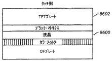
本発明の1つの実施形態によれば、一体化された液晶ディスプレイ・タッチ・スクリーンが提供されている。タッチ・スクリーンは、上にディスプレイ制御回路が形成されている第1基板(例えば、TFTプレート又はアレイ・プレート)と、第1基板に隣接する第2基板(例えば、カラーフィルタ・プレート)を含んでいる。タッチ・スクリーンは、更に、1つ又はそれ以上のタッチ感知要素を含んでおり、全てのタッチ感知要素は、両基板の間に配置されている。 In accordance with one embodiment of the present invention, an integrated liquid crystal display touch screen is provided. The touch screen includes a first substrate (eg, a TFT plate or an array plate) on which a display control circuit is formed, and a second substrate (eg, a color filter plate) adjacent to the first substrate. Yes. The touch screen further includes one or more touch sensitive elements, all of the touch sensitive elements being disposed between both substrates.
両基板の間のタッチ感知要素は、第2基板上に堆積された複数のタッチ駆動電極を、複数のタッチ感知電極にセグメント化された導電ブラック・マトリクスと共に含んでいる。
或いは、両基板の間のタッチ感知要素は、第2基板上に堆積された複数のタッチ駆動電極を、ブラック・マトリクスの裏の複数のタッチ感知金属ラインと共に含んでいてもよく、このブラック・マトリクスはポリマー・ブラック・マトリクスとすることができる。何れの場合も、複数のタッチ駆動電極は、LCDのVCOMの役目も果たすことができるように構成されている。The touch sensing element between the two substrates includes a plurality of touch drive electrodes deposited on the second substrate together with a conductive black matrix segmented into the plurality of touch sensing electrodes.
Alternatively, the touch-sensitive element between the two substrates may include a plurality of touch drive electrodes deposited on the second substrate, together with a plurality of touch-sensitive metal lines behind the black matrix, Can be a polymer black matrix. In either case, the plurality of touch drive electrodes are configured to be able to perform also VCOM role of the LCD.
両基板の間のタッチ感知要素は、更に、基板上に堆積されたパターン形成されていないインジウム−スズ酸化物(ITO)タッチ感知層と、タッチ感知層の周囲に配置された複数のスイッチと、第1のスイッチのサブセットが(例えば、2つの隣接する側から)接続されている第1バスと、第2の複数のスイッチのサブセットが(例えば、他の2つの隣接する側から)接続されている第2バスを含んでいてもよい。タッチ感知層は、第2基板上に堆積され、LCDのVCOMにもなる。各スイッチは、薄膜トランジスタを含んでいてもよい。The touch sensing element between the substrates further comprises an unpatterned indium-tin oxide (ITO) touch sensing layer deposited on the substrate, and a plurality of switches disposed around the touch sensing layer; A first bus to which a subset of the first switch is connected (eg, from two adjacent sides) and a subset of the second plurality of switches (eg, from the other two adjacent sides) The second bus may be included. The touch sensitive layer is deposited on the second substrate and becomes the VCOM of the LCD. Each switch may include a thin film transistor.
両基板の間のタッチ感知要素は、更に、複数の行にパターン形成されたITOタッチ感知層と、複数の行の第1端に配置され、第1バスに接続されている複数のスイッチと、複数の行の第2端に配置され、第2バスに接続されている複数のスイッチと、を含んでいてもよい。タッチ感知層は、第2基板上に堆積され、LCDのVCOMにもなる。各スイッチは、薄膜トランジスタを含んでいてもよい。The touch sensing element between the substrates further includes an ITO touch sensing layer patterned in a plurality of rows, a plurality of switches disposed at a first end of the plurality of rows and connected to the first bus; And a plurality of switches arranged at the second ends of the plurality of rows and connected to the second bus. The touch sensitive layer is deposited on the second substrate and becomes the VCOM of the LCD. Each switch may include a thin film transistor.
両基板の間のタッチ感知要素は、更に、第2基板上に堆積されたセグメント化ITO層と、やはり第2基板上に形成され、各ITOセグメントを、所与の時期に、ディスプレイVCOM、タッチ駆動、又はタッチ感知の内の1つとして構成できるようにする複数のスイッチを含んでいてもよい。各スイッチは、薄膜トランジスタを含んでいてもよい。A touch-sensitive element between the two substrates is further formed on the second substrate, and a segmented ITO layer deposited on the second substrate, each ITO segment being displayed VCOM , at a given time, It may include a plurality of switches that allow it to be configured as one of touch drive or touch sensing. Each switch may include a thin film transistor.
両基板の間のタッチ感知要素は、更に、第2基板上に堆積され、複数のタッチ感知電極にパターン形成されている第1ITO層を、第2基板上に堆積され、複数のタッチ駆動電極にパターン形成されている第2ITO層と共に含んでいてもよい。各タッチ駆動電極は、ディスプレイVCOMに使用することもできる。A touch sensing element between the two substrates is further deposited on the second substrate, and a first ITO layer patterned on the plurality of touch sensing electrodes is deposited on the second substrate and on the plurality of touch drive electrodes. It may be included with the patterned second ITO layer. Each touch drive electrode can also be used for display VCOM .
両基板の間のタッチ感知要素は、更に、第2基板上に堆積され、複数のタッチ駆動電極にパターン形成されている第1ITO層を、第2基板上に堆積され、複数のタッチ感知電極にパターン形成されている第2ITO層と共に含んでいてもよい。各タッチ感知電極は、ディスプレイVCOMに使用することもできる。A touch sensing element between the two substrates is further deposited on the second substrate, and a first ITO layer patterned on the plurality of touch drive electrodes is deposited on the second substrate to form the plurality of touch sensing electrodes. It may be included with the patterned second ITO layer. Each touch sensing electrode can also be used for display VCOM .
両基板の間のタッチ感知要素は、第2基板上に堆積され、複数のタッチ駆動電極と複数のタッチ感知電極とにセグメント化されたITO層を含んでいてもよい。タッチ駆動電極は、抵抗を小さくする金属セグメントを含んでいてもよい。タッチ感知要素は、更に、タッチ駆動電極とタッチ感知電極間の電界の、タッチ感知に有効に寄与しない部分、例えば、機器の外部からユーザーの指又は他のタッチ物体が機器と相互作用するタッチ面に通らない電界部分、を遮断することができるように構成された複数のガード・トレースを含んでいてもよい。 A touch sensing element between both substrates may include an ITO layer deposited on the second substrate and segmented into a plurality of touch drive electrodes and a plurality of touch sensing electrodes. The touch drive electrode may include a metal segment that reduces resistance. The touch sensing element further includes a portion of the electric field between the touch drive electrode and the touch sensing electrode that does not contribute to touch sensing effectively, for example, a touch surface where a user's finger or other touch object interacts with the device from outside the device. A plurality of guard traces configured to be able to block an electric field portion that does not pass through may be included.
両基板の間のタッチ感知要素は、更に、第2基板上に堆積され、複数の個別にアドレス指定可能なタッチ・ピクセルにパターン形成されているITO層を含んでいてもよい。各タッチ・ピクセルは、駆動電極と感知電極を含んでいてもよい。各駆動電極に接続されている複数の駆動ラインと、各感知電極に接続されている複数の感知ラインを設けることもできる。駆動及び/又は感知ラインは、導電ブラック・マトリクスで形成してもよいし、ブラック・マトリクスの裏に設置した金属トレースであってもよく、このブラック・マトリクスは、ポリマー・ブラック・マトリクスとすることができる。 The touch sensitive element between the two substrates may further include an ITO layer deposited on the second substrate and patterned into a plurality of individually addressable touch pixels. Each touch pixel may include a drive electrode and a sense electrode. It is also possible to provide a plurality of drive lines connected to each drive electrode and a plurality of sense lines connected to each sense electrode. The drive and / or sense lines may be formed of a conductive black matrix or metal traces placed on the back of the black matrix, which shall be a polymer black matrix Can do.
両基板の間のタッチ感知要素は、更に、第2基板上に堆積され、各ディスプレイ・ピクセルに対応する少なくとも2つのプレートにセグメント化されている第1ITO層と、第2基板上に配置され、各ディスプレイ・ピクセルに対応するアイランドにセグメント化されている第2ITO層と、ディスプレイのVCOM電極と少なくとも2つのプレートの内の一方との間に接続されているスイッチを含んでいてもよい。この配置では、VCOMをタッチ駆動ラインとして使用できるようになる。この配置では、更に、ディスプレイ・データ・ラインをタッチ感知ラインとして使用できるようになる。The touch sensing element between the two substrates is further disposed on the second substrate, a first ITO layer deposited on the second substrate and segmented into at least two plates corresponding to each display pixel, a first 2ITO layer being segmented into islands corresponding to each display pixel may include a switch connected between the VCOM electrode of the display at least two plates with one of the. In this arrangement, it becomes possible to use the VCOM as a touch drive line. This arrangement also allows display data lines to be used as touch sensitive lines.
両基板の間のタッチ感知要素は、更に、第2基板上に配置された複数のタッチ感知電極にパターン形成されているITO層を、複数のタッチ駆動電極として働くように構成されたディスプレイ選択ライン回路と共に含んでいてもよい。ディスプレイ選択ライン回路は、第1基板上に形成することができる。 The touch sensing element between the substrates further includes an ITO layer patterned on the plurality of touch sensing electrodes disposed on the second substrate, the display selection line configured to serve as the plurality of touch driving electrodes. It may be included with the circuit. The display selection line circuit can be formed on the first substrate.
別の実施形態では、上記各実施形態による一体化されたLCDタッチ・スクリーンを組み込んだ電子機器が提供されている。電子機器は、デスクトップ・コンピュータ、タブレット・コンピュータ、又はノートブック・コンピュータの形態を取ることができる。電子機器は、ハンドヘルド・コンピュータ、携帯情報端末、メディア・プレーヤー、及び携帯電話の形態を取ることもできる。幾つかの実施形態では、機器は、上記の1つ又はそれ以上、例えば、携帯電話とメディア・プレーヤー、を含んでいてもよい。 In another embodiment, an electronic device incorporating an integrated LCD touch screen according to the above embodiments is provided. The electronic device can take the form of a desktop computer, a tablet computer, or a notebook computer. The electronic devices can also take the form of handheld computers, personal digital assistants, media players, and mobile phones. In some embodiments, the device may include one or more of the above, eg, a mobile phone and a media player.
本発明は、添付図面と併せて以下の説明を参照することで理解が最も深まるであろう。 The invention will be best understood by reference to the following description taken in conjunction with the accompanying drawings.
以下の説明は、当業者が本発明を整備し使用できるようにするために提示しており、特定の用途並びにその要件と関連付けて提供している。開示した実施形態に対する様々な修正は、当業者には自明のことであり、ここで定義した一般原則は、本発明の精神と範囲から逸脱すること無く、他の実施形態及び用途に適用することができる。而して、本発明は、ここに示す実施形態に限定されるものではなく、特許請求の範囲と矛盾しない最大の範囲まで許容されるものとする。 The following description is presented to enable one of ordinary skill in the art to make and use the invention and is provided in the context of a particular application and its requirements. Various modifications to the disclosed embodiments will be apparent to those skilled in the art, and the generic principles defined herein may be applied to other embodiments and applications without departing from the spirit and scope of the invention. Can do. Thus, the present invention is not limited to the embodiments shown here, but is allowed to the maximum extent consistent with the claims.
1.LCDとタッチ感知の背景
ここでは、タッチ感知技術を液晶ディスプレイに一体化する技法を開示する。
当業者には既知であるが、LCDは、複数の層、最も基本的には上ガラスと液晶と下ガラス、を含んでいる。上下各ガラスは、特定のディスプレイ・ピクセルの液晶を保有する各セルの境界を与えるため、パターン形成される。上下各ガラスは、更に、導電材料と薄膜トランジスタの様々な層でパターン形成され、各液晶セルを横断する電圧を変化させて液晶の向きを操作し、それによってピクセルの色と明度を制御することができるようになっている。1. LCD and Touch Sensing Background Here, a technique for integrating touch sensing technology into a liquid crystal display is disclosed.
As is known to those skilled in the art, an LCD includes multiple layers, most basically a top glass, a liquid crystal, and a bottom glass. The top and bottom glasses are patterned to provide a boundary for each cell that holds the liquid crystal of a particular display pixel. The upper and lower glasses are further patterned with various layers of conductive materials and thin film transistors to change the voltage across each liquid crystal cell and manipulate the orientation of the liquid crystal, thereby controlling the color and brightness of the pixel. It can be done.
参考文献として援用している各出願に記載されているように、タッチ面、具体的には、マルチタッチ可能透明タッチ面は、一連の層で形成される。一連の層には、少なくとも1つの基板、例えば、ガラスが含まれ、その上に複数のタッチ感応電極が配置される。例えば、相互容量配列なら、非導電層、即ち、ガラスによって分離された複数の駆動電極と複数の感知電極を含んでいる。駆動電極と感知電極の間の容量性結合は、導電性物体(例えば、ユーザーの指)を近づけることで影響を受ける。容量性結合のこの変化を利用して、特定のタッチの場所、形状、大きさ、動き、同一性など、が判定される。それらパラメータは、次に、コンピュータ又は他の電子機器のオペレーションを制御するため、翻訳される。下で説明されている自己容量配列も、当業者には既知のことである。 As described in each application incorporated by reference, a touch surface, specifically a multi-touch capable transparent touch surface, is formed of a series of layers. The series of layers includes at least one substrate, such as glass, on which a plurality of touch sensitive electrodes are disposed. For example, a mutual capacitance array includes a plurality of drive electrodes and a plurality of sensing electrodes separated by a non-conductive layer, ie, glass. Capacitive coupling between the drive and sensing electrodes is affected by bringing a conductive object (eg, a user's finger) closer. This change in capacitive coupling is used to determine the location, shape, size, movement, identity, etc. of a particular touch. These parameters are then translated to control the operation of the computer or other electronic device. The self-capacitance arrangement described below is also known to those skilled in the art.
LCDとタッチ・センサの積層構造を一体化することにより、様々な便益を実現することができる。この一体化には、上記積層構造を組み合わせること又は差し挟むことが含まれる。一体化には、更に、冗長的な構造を無くすこと、及び/又は特定の層又は構造に対して二重の目的(例えば、1つの目的はタッチ機能、もう1つの目的はディスプレイ機能)を見い出すこと、が含まれる。これにより、幾つかの層を無くすことができるようになり、タッチ・スクリーンLCDのコストと厚さを削減すると共に製造を簡素化できるようになる。多種多様な配列が可能であり、ここで、その内の幾つかを更に詳しく論じる。 Various benefits can be realized by integrating the laminated structure of the LCD and the touch sensor. This integration includes combining or interposing the above laminated structures. Integration further eliminates redundant structures and / or finds dual purposes for a particular layer or structure (eg, one purpose is a touch function, another purpose is a display function). That is included. This allows several layers to be eliminated, reducing the cost and thickness of the touch screen LCD and simplifying manufacturing. A wide variety of arrangements are possible, some of which will now be discussed in more detail.
具体的には、一体化されたタッチ・スクリーンLCDの様々な実施形態を下に論じる。
但し、当業者には理解頂けるように、それら各図に関してここに提示している詳細な説明は、一例であり網羅的なものではなく、それら実施形態に対して多くの変更を施すことができる。更に、開示している実施形態の多くは、マルチタッチ可能配列に関するものであるが、教示事項の多くは、シングルタッチ・ディスプレイにも適用することができる。Specifically, various embodiments of an integrated touch screen LCD are discussed below.
However, as will be appreciated by those skilled in the art, the detailed description presented herein with respect to each of these figures is an example and is not exhaustive, and many modifications can be made to these embodiments. . Furthermore, although many of the disclosed embodiments relate to multi-touch capable arrays, many of the teachings can also be applied to single touch displays.
1.1.マルチタッチ感知
同時多発又はほぼ同時多発のタッチ・イベントの認知は、図1に示すマルチタッチ感知配列を使って行われる。マルチタッチ感知配列100は、同時に、ほぼ同時に、異なる時期に、又は或る期間に亘って、タッチ感応面101に亘る複数のタッチ属性(例えば、識別、位置、速度、大きさ、形状、及び強さを含む)を検知し監視することができる。タッチ感応面101は、実質的に互いに独立的に機能し且つタッチ感応面上の異なる各点を表している複数のセンサ点、座標、又はノード102を提供することができる。感知点102は、グリッド又はピクセルアレイに配置され、それぞれの感知点は、信号を同時に生成することができる。感知点102は、タッチ感応面101を、座標システム、例えば、デカルト又は極座標システムへマッピングしたものと考えることができる。1.1. Multi-Touch Sensing Simultaneous or nearly simultaneous multi-touch events are recognized using the multi-touch sensing arrangement shown in FIG. The
タッチ感応面は、例えば、タブレット又はタッチ・スクリーンの形態をしていてもよい。タッチ・スクリーンを製造するには、容量感知点と他の関係付けられた電気構造物を、インジウムスズ酸化物(ITO)の様な実質的に透明な導電性媒体を使って形成する。感知点102の個数と構成は変えることもできる。感知点102の個数は、一般に、所望の解像度及び感受性によって決まる。タッチ・スクリーン用途において、感知点102の個数は、タッチ・スクリーンの所望の透明度によって決まることもある。 The touch sensitive surface may be in the form of a tablet or a touch screen, for example. To manufacture a touch screen, capacitive sensing points and other associated electrical structures are formed using a substantially transparent conductive medium such as indium tin oxide (ITO). The number and configuration of the sensing points 102 can be changed. The number of
下で詳しく説明しているものの様なマルチタッチ感知配列を使用すると、マルチタッチ・センサ101の各ノード102で生成された信号を使用して、特定の時点の各タッチのイメージを作成することができる。例えば、タッチ感応面101に接触しているか近接しているそれぞれの物体(例えば、指、スタイレット、その他)は、図2に示すように、接点パッチ・エリア201を作り出す。各接点パッチ・エリア201は、数個のノード102を範囲に含んでいる。範囲に含まれた各ノード202は物体を検知するが、一方、残りの各ノード102は検知しない。その結果、タッチ面平面のピクセル化イメージ(これを、タッチ・イメージ、マルチタッチ・イメージ、又は近接イメージと呼ぶことにする)が形成される。各接点パッチ・エリア201の信号はまとめてグループ分けされる。各接点パッチ・エリア201は、各点におけるタッチの量に基づき、より高い点とより低い点を含んでいる。イメージ内の接点パッチ・エリア201の形状、並びに高い点と低い点を使用して、互いに密に接している接点パッチ・エリア201が差別化される。更に、現在のイメージを以前のイメージと比較し、物体が時間経過に伴い、どの様に移動したかと、その結果ホスト機器では、どの様な対応動作が行われたかが判定される。 Using a multi-touch sensing array, such as that described in detail below, the signal generated at each
それら感知配列と組合せて、抵抗性、容量性、光学性、その他を含む、多種多様な感知技法が使用できる。容量ベースの感知配列では、物体がタッチ感応面101に近づくと、この物体と当該物体に近接している各感知点102の間に僅かな容量が形成される。この僅かな容量によって生じた感知点102のそれぞれの容量の変化を検知し、それら感知点の位置を観察することによって、感知回路103は、複数のタッチを検知し監視することができる。各容量感知ノードは、自己容量に基づくものでも又は相互容量に基づくものでもよい。 A wide variety of sensing techniques can be used in combination with these sensing arrays, including resistive, capacitive, optical, etc. In a capacitance-based sensing arrangement, when an object approaches the touch
自己容量システムでは、感知点の「自己」容量が、何らかの基準、例えば、接地、と比較して測定される。感知点102は、空間的に分離されている電極であってもよい。それら電極は、駆動回路104と感知回路103に、導電トレース105a(駆動ライン)と105b(感知ライン)によって結合されている。幾つかの自己容量式実施形態では、各電極に対する1つの導電トレースを、駆動ラインと感知ラインの両方として使用することができる。 In a self-capacitance system, the “self” capacitance of the sensing point is measured relative to some reference, eg, ground.
相互容量システムでは、第1電極と第2電極の間の「相互」容量が測定される。相互容量感知配列では、感知点は、空間的に分離された各ラインを形成している、パターン形成された導電体の交差部により形成される。例えば、駆動ラインと感知ラインが各感知点102で互いに交わる、即ち「交差する」ように、駆動ライン105aは第1層上に、感知ライン105bは第2層105b上に、形成される。異なる層は、異なる基板であってもよいし、同じ基板の異なる面であってもよいし、何らかの誘電分離を施した基板の同じ面であってもよい。駆動ラインと感知ラインの間の分離により、各「交差部」に容量性結合が生じる。 In a mutual capacitance system, the “mutual” capacitance between a first electrode and a second electrode is measured. In a mutual capacitive sensing array, the sensing points are formed by intersections of patterned conductors that form spatially separated lines. For example, the
駆動ラインと感知ラインの配列は様々である。例えば、(図示の)デカルト座標システムでは、駆動ラインは横方向の行として形成され、一方、感知ラインは縦方向の列として形成され(又は、その逆であり)、而して、明確に区別できるxとy座標を有していると考えることができる複数のノードを形成する。或いは、極座標システムでは、感知ラインは複数の同心円であって、駆動ラインは半径方向に伸びているラインであり(又は、その逆であり)、而して、明確に区別できる半径及び角座標を有していると考えることができる複数のノードを形成する。何れの場合も、駆動ライン105aは駆動回路104に接続され、感知ライン105bは感知回路103に接続される。 There are various arrangements of driving lines and sensing lines. For example, in the Cartesian coordinate system (shown), the drive lines are formed as horizontal rows, while the sense lines are formed as vertical columns (or vice versa), thus clearly distinguishing Form a plurality of nodes that can be considered as having possible x and y coordinates. Alternatively, in a polar coordinate system, the sensing line is a plurality of concentric circles and the drive line is a radially extending line (or vice versa), thus providing a clearly distinguishable radius and angular coordinate. Form a plurality of nodes that can be considered to have. In any case, the
作動時、駆動信号(例えば、周期的電圧)が、各駆動ライン105aに印加される。駆動されると、駆動ライン105aに印加された電荷は、各ノード102を介して、交差している各感知ライン105bに容量的に結合される。これは、検知可能測定可能な電流及び/又は電圧を、感知ライン105bに発生させる。駆動信号と感知ライン105bに現れる信号の間の関係は、駆動ラインと感知ラインを結合する容量の関数となり、これは、上で指摘したように、ノード102に近接している物体によって影響を受ける。容量感知回路(又は各回路)103は、下で更に詳しく説明するように、感知ライン105bを感知し、各ノードにおける容量を確定する。 In operation, a drive signal (eg, a periodic voltage) is applied to each
上で論じたように、駆動ライン105aは、一度に1つずつ駆動され、その間、他の駆動ラインは接地されている。この処理は、全ての駆動ラインが駆動されるまで、それぞれの駆動ライン105aについて繰り返され、(容量に基づく)タッチ・イメージが、感知結果から構築される。全てのライン105aが駆動されてしまうと、上記シーケンスが繰り返されて、一連のタッチ・イメージが構築される。但し、本発明の幾つかの実施形態では、2007年1月3日出願の米国特許出願第11/619,466号「同時発生感知配列」に記載されているように、複数の駆動ラインが実質的に同時又はほぼ同時に駆動される。 As discussed above, the
図3は、上記配列に対応する相互容量回路300の簡略配線図を示している。相互容量回路300は、駆動ライン105aと感知ライン105bを含んでいて、両ラインは空間的に分離されているので、容量性結合ノード102が形成される。駆動ライン105aは、電圧ソース301に代表される駆動回路104に電気的に(即ち、導電的に)結合されていてもよい。感知ライン105bは、容量感知回路803に電気的に結合されていてもよい。中には、駆動ライン105aと感知ライン105bが共に何らかの寄生容量302を含んでいる事例もある。 FIG. 3 shows a simplified wiring diagram of the
上で指摘したように、駆動ライン105aと感知ライン105の交差部に近接して、導電性物体が存在していなければ、ノード102の容量性結合は、極めて一定に保たれる。
しかしながら、電気伝導性物体(例えば、ユーザーの指、スタイレット、その他)がノード102に近接して来ると、容量性結合(即ち、ローカルシステムの容量)が変化する。
容量性結合が変化すると、感知ライン105bによって搬送される電流(及び/又は電圧)が変化する。容量感知回路103は、容量の変化とノード102の位置を観察し、この情報を何らかの形式でプロセッサ106(図1)に報告する。As pointed out above, the capacitive coupling of the
However, when an electrically conductive object (eg, a user's finger, stylet, etc.) comes in close proximity to
As the capacitive coupling changes, the current (and / or voltage) carried by the
図1を参照すると、感知回路103は、タッチ面101からのデータを捕捉し、捕捉されたデータをプロセッサ106に供給する。幾つかの実施形態では、感知回路103は、生データ(例えば、それぞれの感知点102に対応する容量値のアレイ)をプロセッサ106に送ることができるように構成されている。他の実施形態では、感知回路103は、生データ自体を処理して、処理済みのタッチデータをプロセッサ106に送達することができるように構成されている。何れの場合も、次に、プロセッサは、自身が受け取ったそのデータを使用して、コンピュータ・システム107及び/又は同コンピュータ上で実行されている1つ又は複数のアプリケーションのオペレーションを制御する。上に挙げたものの他にも、上で参照した各出願には様々な実施例が記載されており、それらには、タッチパッド及びタッチ・スクリーンを有する各種コンピュータ・システムが含まれている。 Referring to FIG. 1,
幾つかの実施形態では、感知回路103は、1つ又はそれ以上のマイクロ・コントローラを含んでおり、それらコントローラのそれぞれは、1つ又は複数の感知点102を監視する。各マイクロ・コントローラは、タッチ感応面101からの信号を監視し、監視された信号を処理し、その情報をプロセッサ106に報告するように、ファームウェアで機能する特定用途向け集積回路(ASIC)でもよい。各マイクロ・コントローラは、携帯情報端末(PDS)でもよい。幾つかの実施形態では、感知回路103は、各感知ライン105bの容量を測定し、測定された値をコンピュータ・システム107のプロセッサ106又はホストコントローラ(図示せず)に報告する、1つ又は複数のセンサICを含んでいる。どの様な数のセンサICを使用してもよい。例えば、全ラインに対し1つのセンサICを使用してもよいし、或いは、1つのライン又はライン群に対し複数のセンサICを使用してもよい。 In some embodiments, the
図4は、上に述べた様なマルチタッチ感知配列を操作するためのハイレベルのプロセス400を示している。このプロセスは、複数の感知点102が駆動されるブロック401で開始される。ブロック401に続き、プロセスフローはブロック402に進み、そこで、感知点102からの出力が読み込まれる。例えば、各感知点102毎の容量値が入手される。ブロック402に続き、プロセスはブロック403に進み、そこで、或る1つの瞬間のタッチのイメージ又は他のデータ形式(例えば、信号又は各信号)が作成され、その後、分析されて、タッチ・センサにタッチしているか近接している物体がどこに位置しているかが判定される。ブロック403に続き、プロセスはブロック404に進み、そこで、現在のイメージ又は信号が、1つ又は複数の過去のイメージ又は信号と比較され、それぞれの物体の、形状、大きさ、場所、方向、速度、加速度、圧力、その他の内の1つ又はそれ以上における変化が判定される。この情報は、引き続き、ポインタ又はカーソルの移動から複雑なジェスチャベースの対話まで多岐に亘る、コンピュータ・システム107内での動作を実行するのに使用される(ステップ405)。 FIG. 4 shows a
1.2.トランスフレクティブLCD
タッチ感知技法とトランスフレクティブLCDの一体化を更に深く理解するためには、トランスフレクティブLCDを簡単に紹介することが助けになろう。以下は、低温ポリシリコン(LTPS)トランスフレクティブLCDの典型的なサブピクセルセルの概括である。1.2. Transflective LCD
To better understand the integration of touch-sensing techniques and transflective LCDs, a brief introduction to transflective LCDs will help. The following is a summary of typical subpixel cells of a low temperature polysilicon (LTPS) transflective LCD.
1.2.1.回路の基本原則
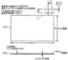
図5は、LTPSトランスフレクティブ・サブピクセル500の代表的なレイアウトを示している。所望のグレイレベルを表している電圧がデータバス501に印加され、選択ライン502がアサートされると、ディスプレイ情報は、サブピクセルのコンデンサーCSTとCLC(図示せず)に転送される。選択ライン502のアサーションレベルは、ゲート駆動正供給電圧に近くなっている。選択ライン502がアサートされている間、VCST(及び、図示していないVCOM)の電圧は一定である。図5に示している全ての回路要素は、金属、ポリ、アクティブ、酸化物、及びITOを含んでおり、それらは、LCDの下ガラス側に製作することができる。1.2.1. Basic Circuit Principles FIG. 5 shows an exemplary layout of the
図6は、低温ポリシリコン(LTPS)LCD600の簡略化モデルを示しており、上面図601と側面図602を含んでいる。上面図601は、ディスプレイ・エリア604と非ディスプレイ・エリア605、両エリア内の、下ガラス608側のVCST経路603の透視図を示している。側面図602は、ディスプレイの断面を示している。FIG. 6 shows a simplified model of a low temperature polysilicon (LTPS)
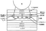
各ディスプレイ行は、VCST606と選択(図示せず)の横トレースを含んでいる。選択トレースは、同じく図示していないポリシリコン薄膜トランジスタ(p−Si TFT)で構成されているゲート駆動回路に接続されている。各VCSTトレース606は、ディスプレイの縁から縁まで走っており、例えば、左手に示す様に一体に接続されている。VCSTトレースは、導電ドット607を介して、上ガラス610側のITO面609にも接続されている。通常、VCOM面をVCOMDrive611に接続するのに、それぞれの隅に1つずつ、4つの導電ドットが使用される。図6は、分かり易くするために、1つのドット607しか示していない。VCSTと上ガラスITO609の電圧は、VCOMDriveによって設定され、このVCOMDriveは、LCDドライバIC(図示せず)によって提供することができる。VCSTは、VCOMDrive611以外の別の駆動ソースに接続されていてもよい。Each display row includes
図7は、サブピクセルの回路図700を示しており、そのガラス基板上に、各種構成要素が製作されていることを示している。下ガラス701は、全てのTFTピクセル回路703を一体化するための基板である。これは、選択ライン・ドライバと制御論理を含んでいる。下ガラスは、LCDドライバ(図示せず)の様なチップ・オン・ガラス(COG)構成要素のための基板の役目も果たしている。コンデンサーCLCの上側電極304は、上ガラス702側に配置されている。電極704は、ディスプレイ・エリアの全域を覆い、CLCを構成している下側電極705に対する対極を形成する、ITIO面とすることができる。上側電極704は、例えば、4つの隅に設置された導電ドット706(1つだけを図示)を介して、下ガラス701側のVCOMDrive707にも接続されている。FIG. 7 shows a circuit diagram 700 of the subpixel, showing that various components are fabricated on the glass substrate. The
1.2.2.VCOM
液晶(LC)を横切る電圧のDC成分を最小化又は無くせば、幾つかの望ましくないイメージアーチファクトを低減又は無くすことができる。従って、LCを横切る電界は、2つの電界方向の間で全体的な均衡を保ちながら周期的に反転される。完璧な電界均衡を得ることは困難であり、その結果、僅かなDCオフセットが生じて、好ましくないイメージアーチファクトが生まれる恐れがある。DCオフセットに起因するちらつきを覆い隠すために、当業者には既知の幾つかの反転理論体系の内の1つ、例えば、ドット反転、を採用することができきる。1.2.2. VCOM
By minimizing or eliminating the DC component of the voltage across the liquid crystal (LC), some unwanted image artifacts can be reduced or eliminated. Thus, the electric field across the LC is periodically reversed while maintaining an overall balance between the two electric field directions. Obtaining perfect electric field balance is difficult and can result in slight DC offsets and undesirable image artifacts. One of several inversion theory schemes known to those skilled in the art, such as dot inversion, can be employed to obscure the flicker due to DC offset.
1.2.3.VCOMの変調
幾つかの実施形態では、データ・ドライバの電圧範囲を縮小するのが望ましい場合もある。従って、VCOMITO面とVCSTトレースを、接地から供給レールに変調し、LCを横切るAC電圧を作り出してもよい。但し、これは、利用可能な転換方法をフレームタイプとラインタイプのみに限定することになる。1.2.3. VCOM Modulation In some embodiments, it may be desirable to reduce the voltage range of the data driver. Thus, the VCOM ITO plane and VCST trace may be modulated from ground to the supply rail to create an AC voltage across the LC. However, this limits the available conversion methods to frame type and line type only.
VCOMDriveの要件は、極めて単純であり、即ち、その電圧が、或るピクセル行について電荷移動が完了し、而してそれらのグレイレベルが設定されるまで、一定に留まる、というものである。一旦、ディスプレイ・ピクセルが設定されてしまえば、VCOMDriveは、サブピクセルに出入りする寄生経路が小さいままであることを前提に、LC状態に顕著な影響を及ぼすこと無く変化することができる。The requirement for VCOM Drive is very simple: the voltage remains constant until charge transfer is complete for a pixel row and thus their gray level is set. . Once the display pixel is set, VCOM Drive can change without significantly affecting the LC state, assuming that the parasitic path to and from the sub-pixel remains small.
1.2.4.定VCOM
VCOM変調は、タッチ感知とLCDとの一体化を複雑化する恐れがある。それら複雑化を克服するための各種技法を下に論じる。液晶を横切る電圧のDC成分を最小化する代わりの方法を採用してもよい。その様な代わりの方法の1つが、J.HectorとP.Buchschacherによる“Low Power Driving Options for an AMLCD Mobile Display Chipset”,SID 02 Digest,pp.695−697に開示されており、同文献を参考文献としてここに援用する。この代わりの方法は、VCOMを定電圧に留めることができるようにするので、広電圧範囲データ・ドライバは不要となり、電力消費を下げることができる。
定VCOMを利用することの様々な利点を下に説明する。1.2.4. Constant VCOM
VCOM modulation can complicate the integration of touch sensing and LCD. Various techniques for overcoming these complications are discussed below. An alternative method of minimizing the DC component of the voltage across the liquid crystal may be employed. One such alternative method is J. Vector and P. “Low Power Driving Options for an AMLCD Mobile Display Chipset” by Buchschacher,
Various advantages of using constant VCOM are described below.
1.3.LCD製造
LCDパネルの製造は、マザーガラスと呼ばれる大きなガラス片にバッチ工程を採用して行われる。マザーガラスは、カラーフィルタ、ブラック・マトリクス、及びCLCの上側電極の基板となる上マザーガラスと、アクティブ・マトリクスTFTアレイと駆動回路の基板となる下マザーガラス、の2片が使用される。1.3. LCD Manufacture LCD panels are manufactured using a batch process on large pieces of glass called mother glass. Mother glass, a color filter, black matrix, and the upper mother glass serving as the substrate of the upper electrode of the CLC, the lower mother glass serving as a substrate of an active matrix TFT array driving circuit, the two pieces of used.
LCD製造の基本的なプロセスフローを図8に示している。2枚の大きなマザーガラス・シートが、LCDの上部分用に1枚と下部分用に1枚として、別々の加工工程801と802を通された後、整列され(ブロック803)、一体にプレスされて、熱処理を施され(ブロック804)、上ガラスと下ガラスの間のシールを硬化させ、これにより、安定したパネル構造が作り出される。次いで、大型パネルは、所望の寸法の、より小型のモジュールに罫書かれ、切断される(ブロック805)。個々のモジュールは、縁部を研磨した(ブロック806)後に、液晶が充填される(ブロック807)。充填後、モジュールはシールされる(ブロック808)。ポラライザーと電気的構成要素が取り付けられる(ブロック809)。フレキシブルプリント回路(FPC)が、加工工程の終了又は終了間際に、それぞれの基板に取り付けられる(ブロック810)。 A basic process flow of LCD manufacturing is shown in FIG. Two large mother glass sheets are passed through
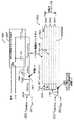
完成したLCDモジュール900を図9に示している。図示のLCDモジュールは、下ガラス902に取り付けられたチップ・オン・ガラス(COG)LCDドライバ901を含んでおり、更に、下ガラス902に取り付けられたフレックス・オン・ガラス(FOG)フレキシブルプリント回路(FPC)903を含んでいる。両構成要素は、下ガラスパッドに電気的に接続され、異方性導電性接着剤(ACA)を使って所定の位置に保持されている。下ガラス902は、上ガラス904からはみ出していて、COG LCDドライバ901、FPC903、及び他の支援構成要素を搭載するための棚905を提供している。ハンドヘルド機器では、データを管理しLCDを制御するシステム・プロセッサ・ボードは、バックライト906の下方に設置される。 The completed
タッチ感知を支援するのに使用される追加の各構成要素(例えば、FPC)を、棚905に取り付けることもできる。他の各取り付け位置も可能である。詳細は、下で説明している関連の実施形態と併せて説明する。 Each additional component (eg, FPC) used to support touch sensing can also be attached to
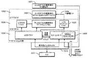
1.4.LCDとタッチ感知を組み合わせる
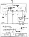
ここで論じる積層構成図は、図10と図11のブロック図に関連付けると更に深く理解されるであろう。一番上から始めて、タッチ感知電極1001、1101が、LCD上ガラス1002、1102の一番上(ユーザー側)に配置されている。タッチ駆動電極1003、1103は、上ガラス1002、1102の底面にパターン形成されている。導電ドット1004、1104が、駆動電極1003、1103を、同じく下ガラス1006、1106に設置されているドライバ1005、1105に接続している。下ガラス1006、1106側の棚1007、1107は、LCDドライバ・チップ1008、1108と、タッチ・センサ・ドライバ・チップ1009を収容しており、LCDドライバ・チップとタッチ・センサ・ドライバ・チップは、互いにインターフェースしていてもよいし(図10)、又は1つの構成要素に一体化されていてもよい(図11)。最後に、同じく棚に接合されているFPC1010、1110が、ホスト機器1011、1111に接続されている。1.4. Combining LCD and Touch Sensing The stackup diagram discussed here will be better understood in connection with the block diagrams of FIGS. Starting from the top, the
2.一体化オプション
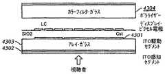
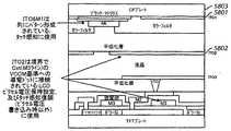
一体型タッチ感知を備えたLCDの幾つかの実施形態は、上ガラスと下ガラスを含んでいる。2つのガラス層の間の液晶の層を通過する光の量に影響を及ぼすため、ディスプレイ制御回路を、それらガラス層の一方及び/又は両方に形成することができる。上ガラスと下ガラスの外部縁の間の空間は、ここでは液晶モジュール(LCM)と呼ばれている。2. Some embodiments of LCDs withintegrated optional integrated touch sensing include a top glass and a bottom glass. Display control circuitry can be formed in one and / or both of the glass layers to affect the amount of light passing through the liquid crystal layer between the two glass layers. The space between the outer edges of the upper and lower glasses is referred to herein as a liquid crystal module (LCM).
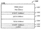
代表的なLCD積層構成1200は、通常、図12に示す様に、追加の層を含んでいる。図12では、ハードコートされたPMMA層1201が、LCDポラライザー1202と上ガラス1203を保護しており、第2ポラライザー1205は、下ガラス1204とバックライト1206の間に含まれている。 A
タッチ感知技術をLCDへの一体化するのは、各種技法を使用して実現することができる。例えば、異なるタッチ感知要素及び/又は層を、LCDディスプレイに組み込むことができ、実施形態が違えば、ディスプレイ及び/又は製造のコスト、ディスプレイの大きさ、ディスプレイの複雑性、ディスプレイの耐久性、ディスプレイの機能性、イメージ表示品質の様な要素が変動することになる。幾つかの実施形態では、タッチ感知能力は、タッチ感知要素をLCMの外部のLCDディスプレイ上に一体化することにより、LCDの中に含ませることができる。他の実施形態では、タッチ感知要素は、LCM内部(例えば、2つのガラス層の間)のみならずLCMの外部にも追加されている。更に他の実施形態では、タッチ感知要素のセットが、LCM内部(例えば、2つのガラス層の間)だけに追加されている。以下の節では、上記実施形態のそれぞれに合わせた複数のコンセプトを説明する。 Integration of touch-sensing technology into the LCD can be accomplished using various techniques. For example, different touch-sensitive elements and / or layers can be incorporated into an LCD display, and different embodiments may cost the display and / or manufacturing, display size, display complexity, display durability, display Factors such as functionality and image display quality will fluctuate. In some embodiments, touch sensing capability can be included in the LCD by integrating the touch sensing element on the LCD display external to the LCM. In other embodiments, touch sensitive elements are added not only inside the LCM (eg, between two glass layers) but also outside the LCM. In yet other embodiments, a set of touch sensitive elements is added only inside the LCM (eg, between two glass layers). In the following sections, a number of concepts tailored to each of the above embodiments will be described.
2.1.液晶モジュールの外部のタッチ感知
LCMの外部にタッチ感知要素を追加すれば、代表的なLCDの製造慣行に殆ど又は全く影響を与えずに、LCDディスプレイにタッチ感知能力を追加できるようになる。例えば、タッチ感知システムとLCDディスプレイシステムを別々に製作し、最終工程で一体化して、タッチ感知能力を有するLCDを形成してもよい。LCMの外部にタッチ感知要素を設ければ、ユーザーがタッチするエリアの近くにタッチ感知要素を設置できるようになり、ディスプレイとタッチ構成要素の間の電気的干渉を小さくできる可能性がある。2.1. Touch Sensing Outside the Liquid Crystal Module Adding touch sensing elements outside the LCM allows touch sensing capabilities to be added to the LCD display with little or no impact on typical LCD manufacturing practices. For example, the touch sensing system and the LCD display system may be separately manufactured and integrated in the final process to form an LCD having touch sensing capability. Providing a touch sensing element outside the LCM allows the touch sensing element to be placed near the area where the user touches and potentially reduces electrical interference between the display and the touch component.
コンセプトCとコンセプトNとして識別されている以下の2つの実施形態では、その様な外部タッチ感知要素を組み込むことができる。 In the following two embodiments, identified as concept C and concept N, such external touch sensing elements can be incorporated.
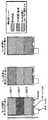
2.1.1.コンセプトC
本発明の1つの実施形態であるコンセプトCは、タッチ機能をLCDから切り離せるようにした、図13に示す積層構成を採用している。コンセプトCでは、2つの追加のインジウム−スズ酸化物(ITO)層(ITO1 1301とITO2 302)が、カラーフィルタ(CF)プレート(例えば、上ガラス層)の上にパターン形成されている。これらの層は、タッチ・センサ、例えば、相互容量タッチ・センサ、のタッチ感知及びタッチ駆動各要素に使用することができる。それらITO層は、列及び/又は行にパターン形成され(図1と図2に示し、先のマルチタッチ感知についての記述で説明)、ガラス基板か薄い(例えば、5〜12mm)SiO2層の様な誘電体1305で分離される。2.1.1. Concept C
Concept C, which is one embodiment of the present invention, employs a stacked configuration shown in FIG. 13 in which the touch function can be separated from the LCD. In Concept C, two additional indium-tin oxide (ITO) layers (ITO1 1301 and ITO2 302) are patterned on a color filter (CF) plate (eg, an upper glass layer). These layers can be used for touch sensing and touch drive elements of a touch sensor, eg, a mutual capacitive touch sensor. The ITO layers are patterned in columns and / or rows (shown in FIGS. 1 and 2 and described above in the description of multi-touch sensing) and are made of a glass substrate or a thin (eg, 5-12 mm) SiO2 layer.
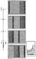
幾つかの実施形態では、タッチ要素に使用される電極パターンは、目に見えるアーチファクトを低減するよう最適化される。例えば、図14は、目に見えるアーチファクトを低減することができるダイヤモンド電極パターンを示している。 In some embodiments, the electrode pattern used for the touch element is optimized to reduce visible artifacts. For example, FIG. 14 shows a diamond electrode pattern that can reduce visible artifacts.
コンセプトCでは、タッチ感知データを搬送するFPCは、上ガラス1303の表面に取り付けられる。 In concept C, the FPC carrying touch sensitive data is attached to the surface of the
2.1.2.コンセプトN
本発明の1つの実施形態であるコンセプトNは、自己容量感知を利用して、カラーフィルタ(CF)プレートの外部面に容量感知を実装することができる。コンセプトNは、タッチ感知構成要素をCFプレート1501(上ガラス)の上に設置した、図15に示す積層構成を使用している。コンセプトNに基づくLCDは、標準的LCD製作工程を変更すること無しに、例えば、従来のTFTプレート1504で使用されるものと同じLTPS工程を利用して、CF面1501上に2層の金属層とパターン形成されたITO1500でTFT1503を形成することにより構築することができる。タッチITO層1500は、複数のタッチ・ピクセル1612にパターン形成されている(図16)。タッチITO層1500は、プラスチックカバー1702(図17に図示)によって保護され、ユーザーにタッチされる面としても機能する。2.1.2. Concept N
One embodiment of the present invention, Concept N, can utilize self-capacitance sensing to implement capacitive sensing on the outer surface of the color filter (CF) plate. Concept N uses the stacked configuration shown in FIG. 15 with the touch sensitive components installed on a CF plate 1501 (top glass). An LCD based on Concept N uses two same metal layers on the
図16は、コンセプトNの自己容量タッチ・ピクセル回路を示している。各ITOタッチ・ピクセル1612は、2つのTFT、例えば、入力TFT1604と出力TFT1608に接続されている。入力TFT1604は、ITOタッチ・ピクセル1612を帯電させ、一方、出力TFT1608は、ITOタッチ・ピクセル1612を放電させる。移動する電荷の量は、指を近づけることで変化するITOタッチ・ピクセル1612の容量によって決まる。自己容量タッチ感知の更なる詳細は、上で説明しており、また、2002年11月27日発行の米国特許第6,323,846号「手動入力を一体化するための方法と装置」に記載されており、その全内容を参考文献としてここに援用する。 FIG. 16 shows a concept N self-capacitance touch pixel circuit. Each
1つの実施形態では、図16と図18の出力列1610‘C0’と出力ゲート1601‘R3’に示すように、出力列1610は、縦方向に各タッチ・ピクセルに共有されており、出力ゲート1606は、横方向に各タッチ・ピクセルに共有されている。図19は、タッチ・ピクセルの詳細なレイアウトを示している。 In one embodiment, output column 1610 is shared by each touch pixel in the vertical direction as shown in output column 1610′C0 ′ and output gate 1601′R3 ′ in FIGS. 1606 is shared by each touch pixel in the horizontal direction. FIG. 19 shows a detailed layout of touch pixels.
2.2.部分的に一体化されたタッチ感知
タッチ感知要素をLCM内部に一体化することは、様々な利点をもたらす。例えば、タッチ感知要素をLCM内部に追加すれば、ディスプレイ機能にしか使用することができなかったITO層又は他の構造を「再使用」して、タッチ感知の機能性をも提供することができるようになる。タッチ感知特性を既存のディスプレイ層に組み込むことで、合計層数を減らすことができ、これにより、ディスプレイの厚さが薄くなり、製造行程を簡素化することができる。2.2. Partially integrated touch sensing The integration of touch sensitive elements within the LCM provides various advantages. For example, the addition of touch-sensing elements within the LCM can also “reuse” ITO layers or other structures that could only be used for display functions to provide touch-sensing functionality. It becomes like this. Incorporating touch-sensing characteristics into an existing display layer can reduce the total number of layers, thereby reducing the thickness of the display and simplifying the manufacturing process.
以下の実施形態では、タッチ感知要素をLCM内部と外部に含ませることができる。タッチ感知要素をLCM内に一体化することは、結果的に、2つの機能の間にノイズと干渉を生じさせるので、以下の設計には、両者の間の電気的干渉によって引き起こされるディスプレイ及び/又はタッチ感知出力に対するあらゆる悪影響を低減又は排除しながら、各要素を共有できるようにする、技法も含まれている。 In the following embodiments, touch sensitive elements can be included inside and outside the LCM. Since integrating touch sensitive elements within the LCM results in noise and interference between the two functions, the following design includes a display and / or caused by electrical interference between the two functions. Alternatively, techniques are included that allow each element to be shared while reducing or eliminating any adverse effects on the touch sensitive output.
2.2.1.コンセプトA
コンセプトAは、マルチタッチ可能(“MT”)ITO感知層(ITO1)2001が、上ガラス2002のユーザー側、上ガラスとポラライザー2003の間に配置されている、図20に示す基本的積層構成2000を使用することができる。一番上から始めて、タッチ感知層は、ITO1 2001(N個の感知(又は駆動)ラインにパターン形成することができるITO層)と、ITO2 2004(M個の駆動(又は感知)ラインにパターン形成することができるITO層)を含んでいる。ITO2 2004は、LCDのVCOM電極の役目も果たす。2.2.1. Concept A
Concept A is a basic
2.2.1.1.コンセプトA:タッチ・センサ電極
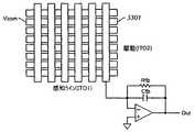
タッチ・センサ電極アレイは、図21(左側)に示している、パターン形成された2つのITO層を含んでいる。図21は、タッチ・センサ電極の1つの可能な実装の簡略図である。視聴者に近接している層、即ちITO 2101が、タッチ出力層となり、この層は感知層又は感知ラインとも呼ばれる。タッチ駆動層2102は、層ITO2側に在る。
ITO2は、コンデンサーCLC(図7参照)の上側電極も形成している。図21(右側)は、更に、3つの感知ピクセル2103a、2103b、及び2103cの詳細を、関係付けられたコンデンサーと共に示している。感知ラインと駆動ラインは、共に、ピッチが5mmで10乃至30ミクロンのギャップを設けている。ギャップは、裸眼で見えない程度に小さく、但し、単純な近接マスクで容易にエッチングできる程度に大きければよい。(図のギャップはかなり誇張されている。)2.2.1.1. Concept A: Touch Sensor Electrode The touch sensor electrode array includes two patterned ITO layers as shown in FIG. 21 (left side). FIG. 21 is a simplified diagram of one possible implementation of touch sensor electrodes. The layer close to the viewer, ie
ITO2 forms also an upper electrode of the capacitor CLC (see FIG. 7). FIG. 21 (right side) further shows details of the three
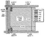
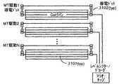
図22は、コンセプトAの1つの可能な物理的実装を、ケーブル配線とサブシステム配置の上面図2201と側面図2202で示している。上面図2201は、FPC2203(下で更に詳しく論じる)の折り畳まれていない状態の大まかな位置を示している。図14は、個別のタッチレベルシフター/デコーダCOGを使用した唯1つの物理的実装を表している。個別のタッチ構成要素の個数を最小化した代わりのアーキテクチャを、下で論じる。機械的安定性を得るために、FPCは、側面図2201に示すように曲げることができるので、T−タブ2204とB−タブ2205の結合部に掛る応力は最小化される。
図23は、主要な下ガラス構成要素とタッチ感知に使用される上ガラス側のセグメント化されたITO2層2301の1つの可能なアーキテクチャ2300を示しているハイレベル・ブロック図である。上ガラス側のITO2の各セグメント2302は、それぞれ、導電ドット2303を介して、下ガラス側の対応するパッドに接続されている。下ガラス側のパッドは、それぞれ、下で論じているタッチ・ドライバに接続されている。FIG. 22 shows one possible physical implementation of Concept A in
FIG. 23 is a high-level block diagram illustrating one possible architecture 2300 of the main lower glass component and the upper glass side segmented
2.2.1.2.コンセプトA:導電ドット
LCDの隅に設置されている導電ドットは、VCOM電極を駆動回路に接続するのに使用されている。タッチ駆動ラインをタッチ−駆動回路に接続するのに、追加の導電ドットが使用されている。各ドットは、タッチ駆動信号(下で詳しく論じる)に大きな位相遅延を追加することのないように、抵抗が十分に低くなっている。これには、導電ドットの抵抗を10オーム又はそれ未満に制限することが含まれる。必要な収容面積を減らすために、導電ドットの大きさにも制限を課してもよい。2.2.1.2. Concept A: Conductive Dots Conductive dots located at the corners of the LCD are used to connect the VCOM electrode to the drive circuit. Additional conductive dots are used to connect the touch drive line to the touch-drive circuit. Each dot is sufficiently low in resistance to not add a large phase delay to the touch drive signal (discussed in detail below). This includes limiting the resistance of the conductive dots to 10 ohms or less. In order to reduce the required accommodation area, a limit may also be imposed on the size of the conductive dots.
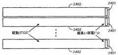
図24に示すように、ドット抵抗と収容面積要件の両方を減らすために、細長い導電ドット2401が使用される。タッチ駆動セグメント2402は幅が約5mmで、ドット抵抗を下げるため、大きな面積を提供している。 As shown in FIG. 24, elongated
2.2.1.3.コンセプトA:フレックス回路とタッチ/LCDドライバIC
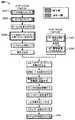
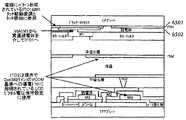
従来のディスプレイ(例えば、図9)は、LCDドライバ集積回路(IC)901を有していて、ディスプレイのローレベル・オペレーションを制御することができるようになっている。システムのホスト・プロセッサは、コマンドとディスプレイデータをLCDドライバ901に送ることによって、ディスプレイに対してハイレベル制御を実行する。マルチタッチ・システムは、更に、1つ又は複数のドライバICを有している。援用している参考文献に記載されている1つの一例的なマルチタッチ可能システムは、3つのIC、即ち、マルチタッチ・コントローラと、外部レベルシフター/デコーダと、ARMプロセッサの様なコントローラと、を含んでいる。ARMプロセッサは、マルチタッチ・コントローラに対してローレベル制御を実行し、このマルチタッチ・コントローラが、次に、レベルシフター/デコーダを制御する。システムのホスト・プロセッサは、ARMプロセッサに対してハイレベル制御を実行し、同プロセッサからタッチデータを受け取る。幾つかの実施形態では、それら各ドライバは、単一のICに集積されている。2.2.1.3. Concept A: Flex circuit and touch / LCD driver IC
A conventional display (eg, FIG. 9) has an LCD driver integrated circuit (IC) 901 that can control the low-level operation of the display. The system's host processor performs high level control on the display by sending commands and display data to the
図25は、タッチ/LCD駆動集積回路2501の一例的なハイレベル・ブロック図を示している。ICには、2つの主要機能、即ち、1)LCD制御と更新、及び2)タッチ走査とデータ処理、がある。これら2つの機能は、LCD制御に使用されるLCDドライバ部分2502と、タッチ走査と処理に使用されるARMプロセッサ2503及びマルチタッチ・コントローラ2504と、によって一体化することができる。各タッチ回路は、一方が他方に干渉することを防ぐために、LCD走査と同期化される。ホストと、LCDドライバ又はARMプロセッサの何れかとの間の通信は、ホスト・データ及び制御バス2505を介することになる。より一体性を高めたタッチ/LCDドライバを下で論じる。 FIG. 25 shows an exemplary high level block diagram of a touch / LCD drive integrated
図26に示すように、様々なタッチ及びディスプレイ層の信号をまとめて運ぶFPC2601は、3つのコネクタタブ、即ち、T−タブ2602、B−タブ2603、及びホスト・タブ2604を有している。T−タブは、上ガラス側の感知ラインパッドに接続されている。T−タブ・トレース2605は、B−タブ2603上の対応するパッドに接続されており、B−タブは下ガラスにも取り付けられている。B−タブ2603は、更に、ホストをタッチ/LCDドライバICに接続できるようにする、ホスト・タブ2604からの通り抜け経路2606を提供している。FPC2601は、タッチ及びLCDオペレーションを支援している各種構成要素2607の基板にもなっていて、2つのパッド2608を介してバックライトFPCにも接続されている。 As shown in FIG. 26, the
FPC2601は、上ガラスと下ガラスの両方に接合されているタブでもよい。或いは、他の接合方法を採用してもよい。 The
2.2.1.4.コンセプトA:下ガラス側に一体化させたタッチ駆動
レベルシフター/デコーダ・チップは、別体の電圧ブースタ(例えば、3V乃至18Vブースタ)と共に、タッチ感知のための高電圧駆動回路を提供する。1つの実施形態では、タッチ/LCDドライバICは、レベルシフター/デコーダ・チップを制御することができる。或いは、電圧ブースタ及び/又はレベルシフター/デコーダは、タッチ/LCDドライバICに一体化してもよい。例えば、その様な一体化は、高圧(18V)LTPS加工を利用して実現することができる。これにより、レベルシフター/デコーダ・チップと電圧ブースタを下ガラスの周辺に一体化することができるようになる。レベルシフター/デコーダは、更に、下で論じるVCOM変調とタッチ駆動のための電圧も提供する。2.2.1.4. Concept A: Touch Drive Integrated on the Lower Glass Side The level shifter / decoder chip, along with a separate voltage booster (eg, 3V-18V booster), provides a high voltage drive circuit for touch sensing. In one embodiment, the touch / LCD driver IC can control the level shifter / decoder chip. Alternatively, the voltage booster and / or level shifter / decoder may be integrated into the touch / LCD driver IC. For example, such integration can be achieved using high pressure (18V) LTPS processing. This allows the level shifter / decoder chip and voltage booster to be integrated around the lower glass. The level shifter / decoder also provides voltages for VCOM modulation and touch drive as discussed below.
2.2.1.5.コンセプトA:タッチ駆動をLCD VCOMと共有
上で論じたように、コンセプトAは、標準的なLCD積層構成に1層のITO層を追加し、それをタッチ感知ラインとして機能させている。タッチ駆動層は、ITO2とも表わされるLCD VCOM面と共有される。ディスプレイ・オペレーションでは、標準的なビデオ・リフレッシュ・レート(例えば、60fps)が使用される。タッチ感知では、少なくとも毎秒120回というレートが使用される。しかしながら、タッチ走査レートは、ディスプレイ・リフレッシュ・レートに一致する毎秒60走査の様な低速に落としてもよい。幾つかの実施形態では、ディスプレイ・リフレッシュ又はタッチ走査の何れかを中断させないことが望ましい場合がある。従って、ディスプレイ・リフレッシュ又はタッチ走査(同じレート又は異なるレートで行われている)を低速化又は中断させること無く、ITO2層を共有化できるようにする案をこれより説明する。2.2.1.5. Concept A: Sharing Touch Drive with LCD VCOM As discussed above, Concept A adds one ITO layer to a standard LCD stack and makes it function as a touch-sensitive line. The touch drive layer is shared with the LCD VCOM surface, also referred to as ITO2. For display operation, a standard video refresh rate (eg, 60 fps) is used. Touch sensing uses a rate of at least 120 times per second. However, the touch scan rate may be reduced to a low rate such as 60 scans per second that matches the display refresh rate. In some embodiments, it may be desirable not to interrupt either the display refresh or the touch scan. Thus, a scheme that allows the ITO2 layer to be shared without slowing down or interrupting display refresh or touch scanning (which is done at the same or different rates) will now be described.
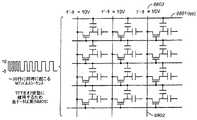
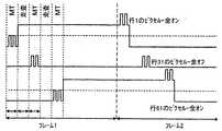
同時に起こるディスプレイ更新とタッチ走査を図27に示している。この実施例には、5つのマルチタッチ駆動セグメント2700、2701、2702、2703、2704が示されている。各タッチ駆動セグメントは、M個のディスプレイ行に重なっている。ディスプレイは、毎秒60フレームで走査され、一方、マルチタッチ・センサ・アレイは毎秒120回走査される。図は、1ディスプレイ・フレームの時間展開が16.67msec持続することを示している。現在更新中のディスプレイのエリアは、アクティブなタッチ駆動セグメントと重ならないのが望ましい。 The simultaneous display update and touch scan are shown in FIG. In this example, five
パッチ2705は、各ディスプレイ行が更新中であることを表している。パッチ2706は、アクティブなタッチ駆動セグメントを表している。図27の左上隅の、ディスプレイ・フレームの開始地点で、1番目のM/2個のディスプレイ・ラインがリフレッシュされる。同時に、タッチ駆動セグメント1 2701は、タッチ感知を目的として駆動される。フレーム内を右に移動して、時間t=1.67msの時点で、次の絵は、次のM/2個のディスプレイ行がリフレッシュ中であり、同時に、タッチ駆動セグメント2 2702が駆動されることを示している。このパターンの約8.3msec後(2番目の行の開始点)には、各タッチ駆動セグメントは既に一度駆動されており、ディスプレイの半分がこれからリフレッシュされることになる。次の8.3msecでは、タッチ・アレイ全体が、再度走査されることになり、而して、走査レートは120fpsとなり、その間、ディスプレイの他方の半分が更新される。 A
ディスプレイ走査は、通常、ライン順に進むので、各タッチ駆動セグメントは、ディスプレイとタッチ活動が重なるのを回避するために、順番通りに駆動されない。図27に示している実施例では、タッチ駆動の順番は、1番目の8.3msec中は1、2、3、4、0であり、2番目の8.3msec期間中は1、2、4、3、0であった。実際の順番設定は、タッチ駆動セグメントの個数とディスプレイ行の個数によって決まる。従って、一般には、タッチ駆動利用の順番をプログラムする能力があることが望ましい。但し、或る特別の場合には、固定された逐時的順番設定で十分である。 Since the display scan typically proceeds in line order, each touch drive segment is not driven in order to avoid overlapping display and touch activity. In the embodiment shown in FIG. 27, the order of touch driving is 1, 2, 3, 4, 0 during the first 8.3 msec, and 1, 2, 4 during the second 8.3 msec period. 3, 0. The actual order setting is determined by the number of touch drive segments and the number of display rows. Therefore, it is generally desirable to have the ability to program the order of touch drive usage. However, in some special cases, a fixed sequential order setting is sufficient.
アクティブなタッチ駆動セグメントを、更新中のディスプレイのエリアから更に遠くに切り離すことが(イメージ品質の理由から)望ましい場合もある。これは図27には示していないが、十分な個数のタッチ駆動セグメント(例えば、6個又はそれ以上のセグメント)が与えられれば、簡単に行うことができる。 It may be desirable (for image quality reasons) to disconnect the active touch drive segment further away from the area of the display being updated. This is not shown in FIG. 27, but can be easily done if a sufficient number of touch drive segments (eg, 6 or more segments) are provided.
そのような技法には、高周波ディスプレイ駆動要素を支援するための多重回路を必要とすること無しに、ディスプレイとタッチ感知の要素毎に異なるリフレッシュ・レートを可能にする効果がある。 Such a technique has the effect of allowing different refresh rates for the display and touch sensitive elements without requiring multiple circuitry to support the high frequency display driving elements.
2.2.1.6.コンセプトA:VCST駆動オプション
図6に示すように、VCSTとVCOMはひとまとめに接続され、而して一体にモジュール化されて、LCを横切る所望のAC波形を実現する。これは、VCOM変調を利用する際、適切なディスプレイ・リフレッシュを実現するのに役立つ。VCOMがタッチ駆動に使用される時、VCSTまで変調する必要はない。これは、下で説明しているように、開回路VCSTオプション(Open VCST Option)と考えることができる。但し、VCSTがVSTMで変調されると、タッチ駆動信号に対する容量性負荷VSTMが減少し、タッチ信号に僅かな位相遅延が生じる恐れがある。これは、下で説明しているDrive VCSTオプション(Drive VCST Option)と考えることができる。2.2.1.6. Concept A: VCST Drive Option As shown in FIG. 6, VCST and VCOM are connected together and thus modularized to achieve the desired AC waveform across the LC. This helps to achieve proper display refresh when using VCOM modulation. WhenVCOM is used for touch drive, it is not necessary to modulate to VCST . This can be considered as described below, the open-circuit VCST Option and (Open VCST Option). However, when VCST is modulated by VSTM , the capacitive load VSTM with respect to the touch drive signal decreases, and there is a possibility that a slight phase delay occurs in the touch signal. This can be thought of as a Drive VCST options that are described below (Drive VCST Option).
図28は、開回路VCSTオプションを示している。下の図2802は、1つのタッチ駆動セグメント2803が、どの様に、M個のディスプレイ行2804に重なるかを示している。上ガラス側に在る各タッチ駆動セグメント2803は、導電ドット2805を介して下ガラス側の各回路に電気的に接続されている。タッチ駆動セグメント下方のM行のM個のVCSTラインは、ディスプレイ2806の縁にひとまとめに接続されている。上の図2801は、自身の別体の蓄積コンデンサーCSTを有する、サブピクセルの基本的な回路を示している。上側の図中のエリア2807は、1つのタッチ駆動セグメントによってカバーされているM個の連続したサブピクセル行を表している。特定のタッチ駆動/ディスプレイ群のディスプレイ・オペレーションとタッチ感知は、上で論じたように、異なる時期に起こる。ディスプレイ・ドライバが、M個の行内の各サブピクセルの状態を設定する用意ができた時、各スイッチ2808、2809は、VCOMDrive2810を、M個のVCSTライン2804と、タッチ駆動セグメント(VCOM)に接続する。VCOMDrive電圧は、LCDドライバにより、反転の位相次第で接地か供給レールの何れかに設定される。その後、このタッチ駆動/ディスプレイ群がタッチ用に利用可能となった時、スイッチ2808、2809は、タッチ駆動セグメントをVSTM2811に接続し、VCSTをVCOMDrive2810から外し、而して、それを開状態2812に置く。FIG. 28 shows the open circuit VCST option. FIG. 2802 below shows how one
図29は、Drive VCSTオプションを示している。下の図2902は、1つのタッチ駆動セグメント2903が、どの様に、M個のディスプレイ行2904に重なるかを示している。上ガラス側に在る各タッチ駆動セグメント2903は、導電ドット2905を介して下ガラス上の各回路に電気的に接続されている。或る特定のタッチ駆動セグメント下方の各行のM個のVCSTラインは、ディスプレイ2906の縁にひとまとめに接続されている。上の図2901は、別体の蓄積コンデンサーCSTを有する、サブピクセルの基本的な回路を示している。上側の図中のエリア2907は、1つのタッチ駆動セグメントによってカバーされているM個の連続したサブピクセル行を表している。ディスプレイ・オペレーションとタッチ感知は、異なる時期に起こる。ディスプレイ・ドライバが、M個の行内の各サブピクセルの状態を設定する用意ができた時、スイッチ2908は、VCOMDrive2910を、M個のVCSTライン2904と、タッチ駆動セグメント(VCOM)に接続する。VCOMDrive2910電圧は、LCDドライバにより、通常は、反転の位相次第で接地か供給レールの何れかに設定される。その後、このタッチ駆動/ディスプレイ群がタッチ用に利用可能となった時、スイッチ2908は、VCSTとタッチ駆動セグメント(VCOM)をVSTM2911に接続する。FIG. 29 shows the Drive VCST option. FIG. 2902 below shows how one
2.2.1.7.コンセプトA:MT−Drive容量性負荷
コンセプトAのタッチ駆動ラインに対する容量性負荷は、例えば、タッチ駆動層と下ガラスの間のギャップが狭く(例えば、〜4μm)、金属ルートとピクセルITOのメッシュで覆うことができるので、高くなっている。液晶は、かなり高い最大誘電定数(例えば、10程度)を有する場合もある。2.2.1.7. Concept A: MT-Drive Capacitive Load Capacitive load on the touch drive line of Concept A is, for example, a narrow gap between touch drive layer and lower glass (eg ~ 4 μm), with metal root and pixel ITO mesh Since it can be covered, it is high. The liquid crystal may have a considerably high maximum dielectric constant (for example, about 10).
タッチ駆動セグメントの容量は、刺激タッチパルスVSTMの位相遅延に影響を及ぼす。
容量が高すぎ、従って位相遅延が過大であれば、得られるタッチ信号に悪意影響が出る。
本発明の発明人が行なった分析の結果は、ITO2シートの抵抗を約30オーム/平方以下に維持すれば、位相遅延を最適限界内に維持できることを示している。The capacity of the touch drive segment affects the phase delay of the stimulation touch pulse VSTM .
If the capacitance is too high and therefore the phase delay is excessive, the resulting touch signal will be maliciously affected.
The results of the analysis performed by the inventors of the present invention indicate that the phase delay can be maintained within optimum limits if the resistance of the ITO2 sheet is maintained below about 30 ohms / square.
2.2.1.8.コンセプトA:電気モデルとVCOM−誘導ノイズ
ITO2は、タッチ駆動とLCD VCOMの両方で同時に使用されることから、VCOMの変調はタッチ信号にノイズを加えることになる。2.2.1.8. Concept A: Electrical Model and VCOM - induced noise ITO2 can be used simultaneously for both touch drive and LCD VCOM, VCOM modulation can add noise to the touch signal.
例えば、或るタッチ駆動セグメントが、別のタッチ駆動セグメントがタッチ感知に使用されているのと同じ時期に、VCOMで変調されると、ノイズ成分がタッチ信号に加わることがある。加わるノイズの量は、VSTMに関するVCOM変調の位相、振幅、及び周波数によって異なる。VCOMの振幅と周波数は、LCDで使用される反転方法によって異なる。For example, if one touch drive segment is modulated withVCOM at the same time that another touch drive segment is used for touch sensing, a noise component may be added to the touch signal. The amount of noise added depends on the phase, amplitude, and frequency of VCOM modulation with respect to VSTM . VCOM of amplitude and frequency varies by an inversion method used in LCD.
図30は、タッチ駆動3001がタッチ感知とLCD VCOM変調の両方に使用される状況に合わせた電気モデルを示している。モデルは、VCOM変調が電荷増幅器3002の入力にノイズを加える恐れのある入力経路を示している。FIG. 30 shows an electrical model for the situation where
幾つかの実施形態では、電荷増幅器3002は、VCOM3003によって誘導されるノイズに対応するための追加的ヘッドルームを必要とする。更に、続くフィルタリング回路(例えば、図示していないが、同期復調器)は、VCOM変調に起因するノイズ信号を取り去る必要がある。In some embodiments,
2.2.1.9.コンセプトA:VSTM効果
或る特定の条件下でのVSTM変調は、変調されるタッチ駆動セグメント下方のサブピクセルの電圧に悪影響をもたらす恐れがある。サブピクセルRMS電圧が判別できるほど変化した場合、ディスプレイ・アーチファクトが生じることがある。結果的に起こる恐れのあるディスプレイの歪を最小限にするために、以下の技法の1つ又はそれ以上を採用することができる。2.2.1.9. Concept A: VSTM Effect VSTM modulation under certain conditions can adversely affect the voltage of the sub-pixel below the modulated touch drive segment. If the subpixel RMS voltage changes appreciably, display artifacts may occur. To minimize display distortion that may result, one or more of the following techniques may be employed.
両面からのタッチ駆動は、LCピクセル電圧の歪を低減することができる。図31に示すように、両面からのタッチ駆動は、下ガラス側に既存の低抵抗CSTルート3101を採用し、VSTMを両面のCSTに導電ドット3102を介して接続することによって実現することができる。或いは、シングルエンド型タッチ駆動なら、全ピクセルにとって均一になるピクセルオフセット電圧を発生させるが、これはデータ駆動レベルを調整することによって低減するか又は無くすことができる。また、ITOシート抵抗を下げることも、ディスプレイ・アーチファクトの低減に役立つ。最後に、VSTMの位相と周波数をVCOMの位相と周波数に結びつけて、タッチ信号のノイズ量を減らすこともできる。Touch drive from both sides can reduce LC pixel voltage distortion. As shown in FIG. 31, the touch drive from both sides, realized by connecting employing existing low resistance CST root 3101 to the lower glass side, through conductive dots 3102 VSTM on both sides of the CST be able to. Alternatively, single-ended touch drive produces a pixel offset voltage that is uniform for all pixels, but this can be reduced or eliminated by adjusting the data drive level. Lowering the ITO sheet resistance also helps reduce display artifacts. Finally, the amount of noise in the touch signal can be reduced by combining the phase and frequency of VSTM with the phase and frequency of VCOM .
2.2.1.10.コンセプトA:製造への影響
コンセプトAの製造プロセスは、典型的なLCD製造プロセスと比べ、追加の工程を含んでいる。幾つかは全く新しい工程であり、また幾つかは既存の工程に修正を加えたものである。図32は、コンセプトAの製造プロセスフローを示している。従来のLCD製造プロセス(例えば、図8のもの)と比べて、ブロック3201、3202、及び3204は、新しい工程を表しており、ブロック3205、3206、及び3207は修正を加えた工程を表している。2.2.1.10. Concept A: Impact on Manufacturing The manufacturing process of Concept A involves additional steps compared to a typical LCD manufacturing process. Some are entirely new processes and some are modifications to existing processes. FIG. 32 shows the manufacturing process flow of Concept A. Compared to a conventional LCD manufacturing process (eg, that of FIG. 8), blocks 3201, 3202, and 3204 represent new steps, and blocks 3205, 3206, and 3207 represent modified steps. .
ITO1の貼付とパターン形成(ブロック3201、3202)は、既知の各方法を使用して行うことができる。ITOは、LCD加工の残りの工程中は保護されている。除去可能な保護被膜を設けるのにフォトレジストを使用してもよい。或いは、シリコン二酸化物なら永久的な保護被覆となる。ITO2は、貼り付けられパターン形成されて(ブロック3204)、同じ様にタッチ駆動セグメントが形成される。 The sticking of ITO1 and pattern formation (
位相遅延の或る分析では、ITO1とITO2のシート抵抗は、何れかの面での容量性負荷が小さければ、小型ディスプレイ(対角線で<=4インチ)では400オーム/平方と高くてもよいことが示されている。上で論じたように、コンセプトAを使用した場合の容量性負荷は、ITO2の最大シート抵抗を約30オーム/平方以下に制限するのが望ましいような大きさである。 In one analysis of phase delay, the sheet resistance of ITO1 and ITO2 may be as high as 400 ohms / square for small displays (diagonal <= 4 inches) if the capacitive loading on either side is small It is shown. As discussed above, the capacitive load using Concept A is such that it is desirable to limit the maximum sheet resistance of ITO2 to about 30 ohms / square or less.
2.2.2.コンセプトA60
コンセプトA60は、物理的にはコンセプトAに似ているが、ディスプレイ更新とタッチ走査を同期化するという問題に対しては異なる対処法を提供している。これは、VCOMの1行反転をタッチ信号に対する刺激(即ち、VSTM)として使用することにより達成することができる。これは、図33に示されており、図では、或る1つのタッチ駆動セグメント3301が、他のタッチ駆動セグメンを定電圧に保ちながら、どの様にして変調されるかを示している。この対処法を使用すれば、迷惑なVCOM誘導ノイズをタッチ信号から除去するという問題は解消することができる。更に、ディスプレイ更新とタッチ・センサ操作を空間的に分離する必要はない。但し、この対処法を使用すれば、復調は、ここに参考文献として援用している、2006年5月2日出願の米国特許出願第11/381,313号「マルチポイント・タッチ・スクリーン・コントローラ」に記載されている多周波変調とは逆で、単一周波(即ち、VCOM変調周波数、例えば、〜14.4kHz)で行われることになる。更に、この対処法を使用すれば、タッチ・センサ走査レートは、ビデオ・リフレッシュ・レート(例えば、毎秒60)に固定することができる。2.2.2. Concept A60
Concept A60 is physically similar to Concept A, but provides a different approach to the problem of synchronizing display updates and touch scanning. This can be accomplished by using a single row inversion of VCOM as a stimulus for the touch signal (ie, VSTM ). This is illustrated in FIG. 33, which shows how one
2.2.3.コンセプトB
図34に示すコンセプトBは、コンセプトAに似ていて、多くの同じ電気的、ケーブル配線的、及び構造的態様を共有している。但し、コンセプトBでは、タッチ駆動層をVCOM層に一体化している。コンセプトBは、従って、LCDとタッチ感知に使用されるITO層の個数と積層位置が異なる。類似性により、コンセプトBについては、コンセプトAとBの相違点に焦点を当てて説明する。2.2.3. Concept B
Concept B shown in FIG. 34 is similar to Concept A and shares many of the same electrical, cabling, and structural aspects. However, in Concept B, the touch drive layer is integrated with the VCOM layer. Concept B therefore differs in the number and stacking positions of the ITO and ITO layers used for touch sensing. Due to the similarity, concept B will be described focusing on the differences between concepts A and B.
コンセプトBでは、コンセプトAの共有型ITO2層を2つのITO層に分割し、1層をタッチ感知(ITO2)3402に使用し、1層をLCD VCOM(ITO3)3403に使用する。一番上から始めて、タッチ感知に使用される層は、N個のタッチ感知ラインにパターン形成されるITO層であるITO1 3401と、M個のタッチ駆動ラインにパターン形成されるITO層であるITO2 3402と、LCDのVCOM電極の役目を果たすITO層であるITO3 3403を含んでいる。タッチ駆動層(ITO2)3402は、上ガラス3404の下表面の、カラーフィルタ3405の上方に堆積されている。In concept B, the shared ITO2 layer of concept A is split into two ITO layers, one layer is used for touch sensing (IT02) 3402 and one layer is used for LCD VCOM (IT03) 3403. Starting from the top, the layers used for touch sensing are
VCOMをタッチ駆動要素から切り離すことで、干渉を低減することができる。By disconnecting VCOM from the touch drive element, interference can be reduced.
2.2.3.1.コンセプトB:タッチ・センサ電極
コンセプトBは、上でコンセプトAについて説明したものと実質的に似ているタッチ・センサ電極を含んでいる。2.2.3.1. Concept B: Touch Sensor Electrode Concept B includes a touch sensor electrode that is substantially similar to that described above for Concept A.
2.2.3.2.コンセプトB:導電ドット
コンセプトAと同様に、コンセプトBでは、タッチ駆動セグメントを専用回路に接続するのに、LCDの各隅に設置された追加の導電ドット3406を使用している。VCOMをタッチ感知と共有する必要がないため、コンセプトBは、VCOMを自分の駆動回路に接続する隅のドットを留保しておくことができる。更に(下で論じているように)、コンセプトBは、VCOM用に更により多くの導電ドットを追加してもよい。2.2.3.2. Concept B: Conductive Dots Like Concept A, Concept B uses additional
2.2.3.3.コンセプトB:フレックス回路及びタッチ/LCDドライバIC
コンセプトBでは、コンセプトAで説明したものと実質的に似ているFPC及びタッチ/LCDドライバICを使用している。2.2.3.3. Concept B: Flex circuit and touch / LCD driver IC
Concept B uses FPC and touch / LCD driver ICs that are substantially similar to those described in Concept A.
2.2.3.4.コンセプトB:LCD走査との同期化
コンセプトBでは、VCOM層をタッチ駆動層から分離することができるが、アクティブなタッチ駆動を更新中のディスプレイ・エリアから物理的に切り離すために、タッチ走査をLCD更新と同期化するのがなお望ましい。先にコンセプトAで説明した同期化案は、コンセプトBでも使用できる。2.2.3.4. Concept B: Synchronization with LCD Scan In Concept B, the VCOM layer can be separated from the touch drive layer, but touch scan is used to physically separate the active touch drive from the display area being updated. It is still desirable to synchronize with the LCD update. The synchronization plan previously described in concept A can also be used in concept B.
2.2.3.5.コンセプトB:MT−Drive容量性負荷
コンセプトAと同様に、コンセプトBのタッチ駆動ラインに対する容量性負荷は大きくてもよい。大容量は、タッチ駆動(ITO2)3402とVCOM面(ITO3)3403の間の誘電体が薄い(例えば、〜5μm)せいである。タッチ刺激信号の望ましくない位相遅延を低減する1つのやり方は、並列金属トレースの追加によってITOライン抵抗を下げることである。位相遅延は、レベルシフター/デコーダの出力抵抗を落とすことによっても低減される。2.2.3.5. Concept B: MT-Drive Capacitive Load Similar to Concept A, the capacitive load on the touch drive line of Concept B may be large. The large capacitance is due to the thin dielectric (eg, ˜5 μm) between the touch drive (ITO2) 3402 and the VCOM surface (ITO3) 3403. One way to reduce the undesired phase delay of the touch stimulus signal is to reduce the ITO line resistance by adding parallel metal traces. Phase delay is also reduced by reducing the output resistance of the level shifter / decoder.
2.2.3.6.コンセプトB:電気モデルとVCOM−誘導ノイズ
VCOM面全体がタッチ駆動層に結合されているため、マルチタッチ電荷増幅器のオペレーションは、VCOM変調により誘導されたノイズで妨害される場合がある。それらの効果を軽減するために、コンセプトBは、定VCOM電圧を有している。2.2.3.6. Concept B: Electrical Model and VCOM -Inductive Noise Since the entire VCOM plane is coupled to the touch drive layer, the operation of the multi-touch charge amplifier may be disturbed by noise induced by VCOM modulation. To mitigate those effects, Concept B has a constant VCOM voltage.
反対に、ITO2 3402とITO3 3403(VCOMとタッチ駆動)の間の結合は、VCOM電圧との干渉を引き起こし、これにより、間違ったデータ電圧がLCピクセルに蓄積される事態を引き起こすことになりかねない。VSTMによるVCOMの変調を低減するために、VCOMを下ガラスに接続している導電ドットの個数を増やすことができる。例えば、ビューイング・エリアのそれぞれの隅のVCOMドットに加えて、それぞれの縁の真ん中に導電ドットを設置してもよい。Conversely, the coupling between
VCOM−VSTM結合により生じる歪は、VSTMとVCOMを同期化し、ピクセルTFTを正に適切な時点でオフにすることにより、更に低減することができる。例えば、ライン周波数が28.8kHzであって、タッチ駆動周波数がこの数倍(例えば、172.8、230.4、及び288kHz)であるとすると、VCOM歪は、全ピクセルにつき、同じ位相関係を有することになり、これによりVCOM歪の目に見える度合いが低減されるか無くなる。更に、歪がほぼ減衰した時にピクセルTFTの各ゲートがオフになれば、LCピクセル電圧エラーは減少する。コンセプトAと同様に、タッチ信号のノイズ量を減少させるために、VSTMの位相と周波数を、VCOMの位相と周波数に結び付けることもできる。The distortion caused by the VCOM -VSTM coupling can be further reduced by synchronizing VSTM and VCOM and turning off the pixel TFT at the right time. For example, if the line frequency is 28.8 kHz and the touch drive frequency is several times this (eg, 172.8, 230.4, and 288 kHz), the VCOM distortion is the same phase relationship for all pixels. This reduces or eliminates the visible degree of VCOM distortion. Furthermore, LC pixel voltage error is reduced if each gate of the pixel TFT is turned off when the distortion is substantially attenuated. Similar to Concept A, the phase and frequency of VSTM can be tied to the phase and frequency of VCOM in order to reduce the amount of noise in the touch signal.
2.2.3.7.コンセプトB:製造への影響
コンセプトAと同様に、コンセプトBでも、LCD製造プロセスに工程が追加されている。図35は、コンセプトBの製造プロセスを示しており、ここでは、従来のLCD製造プロセス(例えば、図8に示しているもの)と比較して、ブロック3501、3502、3503、及び3504は新しい工程を表しており、ブロック3506、3507、3508、及び3509は既存の工程(例えば、同様に図8に比して)に対する修正を表している。2.2.3.7. Concept B: Impact on Manufacturing Like Concept A, Concept B also adds steps to the LCD manufacturing process. FIG. 35 shows the manufacturing process for Concept B, where
コンセプトAと同様に、既知の方法を使用して、ITO1が貼り付けられ(ブロック3501)、パターン形成される(ブロック3502)。ITO1とITO2のシート抵抗も、コンセプトAで説明したものと実質的に似ている。コンセプトBでは、ITO2層の堆積(ブロック3503)は、これがガラスに直接貼り付けられることから、ルーチンとなっている。タッチ駆動セグメントに接続されている導電ドットに関する、ITO2層と下ガラスの間の電気的アクセスは、シャドーマスクを使ったエッチング(ブロック3504)により容易に達成することができる。 Similar to Concept A, ITO1 is applied (Block 3501) and patterned (Block 3502) using known methods. The sheet resistance of ITO1 and ITO2 is also substantially similar to that described in Concept A. In concept B, the ITO2 layer deposition (block 3503) is routine because it is applied directly to the glass. Electrical access between the ITO2 layer and the bottom glass for the conductive dots connected to the touch drive segment can be easily achieved by etching with a shadow mask (block 3504).
シート抵抗が30から100オーム/平方の間にあるITO3(例えば、LCDのVCOM層)も、従来の方法を使用して貼り付けることができる(ブロック3505)。但し、上で論じたように、VCOM電圧歪は、ITO3層の抵抗を小さくすることにより低減される。必要であれば、タッチ駆動セグメントに平行に走る金属トレースを加えることによって、ITO3により低い有効抵抗を実現することができる。金属トレースは、ピクセル開口部に干渉しないように、ブラック・マトリクスと整列される。金属トレースの密度は、VCOM層の所望の抵抗が得られるように、(1ディスプレイ行毎から約32ディスプレイ行毎の間で)調整される。ITO3 (eg, the LCD's VCOM layer) with a sheet resistance between 30 and 100 ohms / square can also be applied using conventional methods (block 3505). However, as discussed above, VCOM voltage distortion is reduced by reducing the resistance of the ITO3 layer. If necessary, a lower effective resistance can be achieved with ITO3 by adding metal traces running parallel to the touch drive segment. The metal trace is aligned with the black matrix so as not to interfere with the pixel openings. The density of the metal traces is adjusted (between every display row to about every 32 display rows) to obtain the desired resistance of the VCOM layer.
2.2.4.コンセプトB’
コンセプトB’は、ITO2駆動層を無くして、代わりに、導電ブラック・マトリクス(例えば、上ガラス下方のCrO2の層)をタッチ駆動層として使用した、コンセプトBの変型であると理解して頂きたい。或いは、金属駆動ラインを、ブラック・マトリクスの裏に隠すこともでき、このブラック・マトリクスは、ポリマーのブラック・マトリクスでもよい。これは、(1)ITO層が不要になる、(2)VCOM層に対するVSTMの効果が小さくなる、及び(3)製造プロセスが簡素化される、を含め幾つかの便益をもたらす。製造プロセスは、タッチ駆動にブラック・マトリクスを使用すると、カラーフィルタ上のITO層をパターン形成する必要が無くなるので、簡素化される。2.2.4. Concept B '
Concept B 'should be understood as a variation of Concept B, with the ITO2 drive layer removed and instead a conductive black matrix (eg, a layer of CrO2 below the top glass) used as the touch drive layer. I want. Alternatively, the metal drive lines can be hidden behind a black matrix, which can be a polymer black matrix. This provides several benefits, including (1) eliminating the need for an ITO layer, (2) reducing the effect of VSTM on the VCOM layer, and (3) simplifying the manufacturing process. The manufacturing process is simplified when a black matrix is used for touch drive, since it is not necessary to pattern the ITO layer on the color filter.
図36は、コンセプトB’の側面図3601と上面図3602を示している。図から分かるように、側面図3601は、ITO3603の最上層がタッチ感知に使用されていることを除けば、標準的なLCD積層構成に非常によく似ている。図36の下の図は、ブラック・マトリクス3604が別々のタッチ駆動セグメントにどの様に分割されるかを示している。メッシュパターンは、それぞれの駆動セグメントが他のセグメントから電気的に絶縁されていることを除けば、従来のブラック・マトリクスのパターンに従っている。ブラック・マトリクス・メッシュをタッチ駆動に使用したことで発生するタッチ信号の強度低下を補償するために、電荷アンプ利得を上げてもよい(例えば、約4X)。 FIG. 36 shows a
タッチ感知層は、VCOM層から遮蔽しなくてもよいので、VCOM変調がタッチ信号に干渉する場合がある。更に、タッチ駆動が、依然としてVCOM電圧に干渉する場合がある。これらの問題は共に、コンセプトAで説明したようにVCOMをセグメント化すること、及び/又は、上述ようにディスプレイ更新とタッチ感知を空間的に切り離すことにより解決される。それらの問題を解決するのに、定VCOM電圧を使用することもできる。Since the touch sensitive layer may not be shielded from the VCOM layer, VCOM modulation may interfere with the touch signal. Furthermore, touch drive may still interfere with the VCOM voltage. Both of these problems are solved by segmenting VCOM as described in Concept A and / or spatially separating display update and touch sensing as described above. A constant VCOM voltage can also be used to solve these problems.
2.2.5.コンセプトK
コンセプトKを、図37(回路図)と図38(積層構成図)に示す。コンセプトKは、CST・オン・ゲート構成を使用した場合、TFT LCDの選択パルスが部分的にピクセルITOに送られる、という事実を利用している。2.2.5. Concept K
Concept K is shown in FIG. 37 (circuit diagram) and FIG. 38 (stacked configuration diagram). Concept K takes advantage of the fact that when using theCST -on-gate configuration, the select pulse of the TFT LCD is partially sent to the pixel ITO.
図38のディスプレイ積層構成に示すように、視聴者は、CFプレート3802ではなくアクティブなアレイ・プレート3801に面している。アクティブなアレイ上のITOピクセル3803は、タッチ・センサのVSTMを提供し、各ディスプレイ行は、VSTMパルス用とディスプレイアドレス指定用に交互に使用されることになる。プラスチック・ポラライザー3805上のITO感知層3804は、アレイ・プレート3801の背面に重ねられ、タッチ感知層を提供している。薄いガラス層(例えば、0.2mm)は、信号対ノイズ比の改善に役立つ。As shown in the display stack configuration of FIG. 38, the viewer faces the
ディスプレイ更新中、各行は、ピクセル・データの更新に個別に選択される(図39に図示)。タッチ感知のためのVSTMを発生させる場合、複数の行4001が同時に選択され、一方で、高いデータ電圧4003が列ライン4002に印加されTFTをオフ状態に保つ(図40に図示)。列ドライバは、タッチ駆動の間隔に対応するため、ディスプレイメモリからのデータ信号のタイミングを調節する。During the display update, each row is individually selected for pixel data update (shown in FIG. 39). When generating VSTM for touch sensing, multiple rows 4001 are selected simultaneously, while a high data voltage 4003 is applied to the column line 4002 to keep the TFTs off (shown in FIG. 40). The column driver adjusts the timing of the data signal from the display memory to accommodate the touch drive interval.
1つの実施形態では、タッチ・パルス・シーケンスは、タッチ走査間隔の間、約30行4001に同時にパルスを送る。図41は、LCDのサブピクセル電圧に対するタッチ駆動パルス(VSTM)の影響を示している。VSTMパルスから追加される電圧は、VCOMのDCオフセット及び/又はディスプレイ・データ・グレイレベルのガンマ補正によって補償される。In one embodiment, the touch pulse sequence sends pulses to about 30 rows 4001 simultaneously during the touch scan interval. FIG. 41 shows the influence of the touch drive pulse (VSTM ) on the subpixel voltage of the LCD. The voltage added from the VSTM pulse is compensated by DC offset of VCOM and / or gamma correction of display data gray level.
コンセプトKは、多くの利点をもたらす。各ディスプレイ・ピクセルと各タッチ・センサは駆動回路を共有するので、レベルシフター/デコーダが不要になる。その上、従来のCFプレートが使用できる。更に、上ガラスと下ガラスの間に余分な導電ドットが必要無くなる。バスライン反射により、ディスプレイの各部分の反射率(R)が高まるため、バスライン下方にRを下げる余分な膜(例えば、Crの下にCrO)を使用する必要が生じる。 Concept K offers many advantages. Since each display pixel and each touch sensor share a driving circuit, a level shifter / decoder is not required. In addition, conventional CF plates can be used. Furthermore, there is no need for extra conductive dots between the upper glass and the lower glass. Since the reflectance (R) of each part of the display is increased by the bus line reflection, it is necessary to use an extra film (for example, CrO under the Cr) that lowers the R below the bus line.
2.2.6.コンセプトX’
コンセプトX’を、図42(回路図)と図43(積層構成図)に示す。コンセプトX’は、VSTMパルスがTFTピクセル・スイッチのゲートパルスに似ているという事実(例えば、15乃至18Vスイング)を利用している。コンセプトX’では、各タッチ駆動セグメント4301は、LTPSアクティブ・アレイの一部であり、ピクセル蓄積コンデンサーCSTの対極を形成している。CSTは、2つのITO層4301と4302の間に形成されている。この実施形態では、カラーフィルタ・プレート4303ではなく、アクティブ・アレイ・プレート4303が、ディスプレイのユーザー側に配置されている。2.2.6. Concept X '
The concept X ′ is shown in FIG. 42 (circuit diagram) and FIG. 43 (lamination configuration diagram). Concept X ′ takes advantage of the fact that the VSTM pulse is similar to the gate pulse of a TFT pixel switch (eg, 15-18V swing). In Concept X ', each touch drive segment 4301 is part of the LTPS active array, to form a counter electrode of the pixel storage capacitor CST. CST is formed between the two ITO layers 4301 4302. In this embodiment, an
図42に示すように、VSTMの3つの異なる周波数4201を有するパルスシーケンスが、3行のピクセル行4202に、これらの行を選択するために共有されている。各ITOタッチ駆動セグメント4203は、アドレス指定された行に隣接する行のセットの下方にパターン形成されている。各タッチ駆動セグメント4203は、VSTMに接続されていない時、各TFT4204によってGNDに接続されている。As shown in FIG. 42, a pulse sequence having three
コンセプトX’を構成するための加工工程に加える変更には以下の事項が含まれる。第1に、パターン形成された感知ITOを、アレイ基板の外部に追加する。第2に、LTPS加工中に、SiO2保護を感知ITO上に追加する。保護レジストを使用してもよい。
第3に、LTPSアレイのために(代表的なLTPSプロセスに見られる)SiO2バリア層の下にタッチ駆動ITOを堆積させパターン形成する。最後に、バリアSiO2にビアをパターン形成して、タッチ駆動ITO層に接触させる。この工程は、その後のプロセス工程と組み合わせてもよい。The changes to be made to the processing steps for constructing the concept X ′ include the following items. First, a patterned sensing ITO is added outside the array substrate. Second, SiO2 protection is added on the sensing ITO during LTPS processing. A protective resist may be used.
Third, touch drive ITO is deposited and patterned under the SiO2 barrier layer (as found in a typical LTPS process) for the LTPS array. Finally, vias are patterned in the barrier SiO2 to contact the touch drive ITO layer. This step may be combined with subsequent process steps.
コンセプトX’は、多くの利点をもたらす。例えば、ディスプレイ及びタッチ・センサが駆動回路を共有するので、レベルシフター/デコーダ・チップを無くすことができる。
その上、CFプレートへの電荷は一切必要としないので、従来のカラーフィルタ加工が使用できる。更に、蓄積コンデンサーCSTは、2つのITO層の間に設置されるので、高い透過率を実現できる。別の利点は、アレイ・プレート4303とCFプレート4304の間の余分な導電ドットを無くすことができることである。Concept X ′ provides many advantages. For example, the level shifter / decoder chip can be eliminated because the display and touch sensor share the drive circuit.
In addition, since no charge is required on the CF plate, conventional color filter processing can be used. Furthermore, since the storage capacitorCST is disposed between the two ITO layers, a high transmittance can be realized. Another advantage is that extra conductive dots between the
2.3.完全に一体化されたタッチ感知
本発明の実施形態の3番目のセットは、タッチ感知要素をLCM内部に完全に一体化している。部分的に一体化されたタッチ感知と同様に、LCM内の既存の層は、二重の業務を果たして、タッチ感知機能性を提供するので、これにより、ディスプレイを薄型化し、製造を簡素化することができる。完全に一体化されたタッチ感知層も、両ガラス層の間で保護されている。2.3. Fully Integrated Touch Sensing A third set of embodiments of the present invention fully integrates touch sensitive elements within the LCM. Similar to partially integrated touch sensing, the existing layers in the LCM serve a dual task and provide touch sensing functionality, thereby thinning the display and simplifying manufacturing. be able to. A fully integrated touch sensitive layer is also protected between the glass layers.
幾つかの実施形態では、完全に一体化されたLCDは、これまでの各実施形態で説明したものと似ているVCOM層を含んでいる。他の実施形態では、完全に一体化されたタッチ感知LCDは、面内切り替え(IPS)LCD構造を含んでおり、それらについて以下の節で更に詳しく説明する。In some embodiments, a fully integrated LCD includes a VCOM layer similar to that described in the previous embodiments. In other embodiments, a fully integrated touch sensitive LCD includes an in-plane switching (IPS) LCD structure, which are described in more detail in the following sections.
2.3.1.完全に一体化されたVCOMベースのLCD
2.3.1.1.コンセプトA’
コンセプトA’は、タッチ感知層として使用される(上ガラス下の)導電ブラック・マトリクス層にとって都合のよいようにITO感知層(図20のITO1 2001)を無くした、コンセプトAの変型と考えることができる。或いは、金属の感知ラインは、ポリマーのブラック・マトリクスとすることができるブラック・マトリクスの裏に隠すこともできる。その結果、コンセプトA’では、FPC上のT−タブと、上ガラスへの対応する接合作業を無くすことができる。各タッチ感知ラインは、導電ドットを介して下ガラスに経路決めされ、タッチ/LCDドライバ・チップに直接接続される。更に、FPCは標準的なLCD FPCであればよい。製造工程及び構成要素を無くすことは、コンセプトAとBに比べコストを削減することに繋がる。2.3.1. Fully integrated VCOM based LCD
2.3.1.1. Concept A '
Concept A ′ is considered a variation of Concept A, which eliminates the ITO sensing layer (
図44は、導電ブラック・マトリクスをタッチ感知層に置き換える1つのやり方を示している。図41は、そのブラック・マトリクス4403が各主要カラー区間4404の間を走っている、或る1つのピクセルの上側部分の側面図4401を含んでいる。タッチ駆動セグメント4405は、誘電層4406を平坦化することにより、ブラック・マトリクス4403から切り離されている。図44は、ブラック・マトリクス・ライン4403が縦方向に走っているディスプレイの上面図も示している。大凡96本のブラック・マトリクス・ライン(例えば、32画素相当)は、ひとまとめに電荷増幅器4907の負端子に接続されている。各タッチ駆動セグメント4405は、上に述べたように駆動される。上ガラス4408に指を近づけると、縦の各ブラック・マトリクス・ライン4403とタッチ駆動セグメント4405の間の電界に摂動が起きる。この摂動は電荷増幅器4407によって増幅され、本明細書の別の個所で説明しているように更に処理される。 FIG. 44 illustrates one way to replace the conductive black matrix with a touch sensitive layer. FIG. 41 includes a side view 4401 of the upper portion of a pixel whose
ディスプレイ内の各タッチ感知ライン4403の深さのために、指又はタッチ物体と各感知ライン4403の間の最小距離が制限される。これにより、タッチ信号の強度が低下する。これは、タッチ感知層の上方の各層の厚さを薄くして、指又は他のタッチ物体が各感知ラインに一層接近することができるようにすることによって、解決される。 Due to the depth of each
2.3.1.2.コンセプトX
コンセプトXを、図45と図46に示す。図45に示すコンセプトXの積層構成は、基本的には、標準的なLCDのものと同じである。タッチ感知層4501は、VCOM層(ITO2)内に埋め込まれており、VCOM電圧面を提供することとタッチ・センサの出力の役目を果たすことの二重の目的を果たす。タッチ駆動層は、既存のLCD層内に埋め込むこともできる。例えば、タッチ駆動は、下ガラス4503側に設置し、LCD選択ライン回路の一部としてもよい(図5参照)。選択回路は、而して、サブピクセルTFTのゲート信号とタッチ駆動信号VSTMを提供するという二重の目的を果たす。図46は、その浮動ピクセル4601がVCOM層に埋め込まれたタッチ感知層の1つの可能な配列を示している、コンセプトXの上面図である。2.3.1.2. Concept X
Concept X is shown in FIGS. 45 and 46. FIG. The stacked structure of concept X shown in FIG. 45 is basically the same as that of a standard LCD.
2.3.1.3.コンセプトH
コンセプトHを、図47から図50に示す。コンセプトHは、上ガラス又はディスプレイのプラスチック層外部に一切ITOを含んでいる必要はない。その結果、製造プロセスは、既存のディスプレイ製造プロセスに非常に似たものとなる。2.3.1.3. Concept H
Concept H is shown in FIGS. Concept H does not need to contain any ITO outside the top glass or plastic layer of the display. As a result, the manufacturing process is very similar to existing display manufacturing processes.
図47に示すように、スクリーンのタッチ感知部は、透明な抵抗性シート4701、例えば、パターン形成されていないITOの層を上に堆積させたガラス又はプラスチック基板とすることができる。ディスプレイのVCOM層をこのタッチ感知部に使用してもよい。
この層は、パターン形成する必要がないため、上で論じた幾つかの実施形態と比較して、フォトリソグラフィ工程を製造プロセスから無くすことができる。説明し易くするため、各側面を、図に示す様に、北、南、東、及び、西と呼ぶことにする。As shown in FIG. 47, the touch sensing portion of the screen may be a transparent
Since this layer does not need to be patterned, a photolithography step can be eliminated from the manufacturing process compared to some embodiments discussed above. For ease of explanation, each side will be referred to as north, south, east, and west as shown in the figure.
複数のスイッチ4702が、抵抗性シートの周囲周りに配置されている。それらスイッチは、ガラス上にTFTとして実装されている。各スイッチの場所に、複数の導電ドット4703が示されており、ディスプレイの境界領域で、VCOM(上ガラス側)を下ガラス側のTFT層に接続している。スイッチ4702は、まとめて2つのバスに接続されており、例えば、北と東のスイッチは1つのバス4704に接続され、南と西のスイッチは第2バス4705に接続されている。A plurality of
タッチ感知では、各スイッチ4702は、以下のように作動する。北と南のスイッチは、Y方向の容量を測定するのに使用される。左と右側のスイッチは、X方向の容量を測定するのに使用される。北東と南西の隅のスイッチは、XとY両方の測定に使用される。容量は、図49に示すように、抵抗性シート4701を変調波形VMODで刺激することによって測定される。シートを所望電圧まで駆動するのに必要とされる電流(即ち、電荷)が測定され、タッチの場所を求めるのに使用される。In touch sensing, each
具体的には、図49の波形に示すように、タッチが無い場合、基線容量4902は、シート4701をVMOD電圧まで刺激するのに要する電流(電荷)を表している。タッチがあると、指の容量のために、より高い電流4903(電荷)が必要となる。このより高い電流は、下側の波形群に示されている。次に、タッチの場所が、図49に示す基線と信号波形の単純な数学的組合せにより求められる。Specifically, as shown in the waveform of FIG. 49, when there is no touch, the
X方向(即ち、東−西)測定中のタッチ・スクリーンの等価回路を図48に示す。C_PARA4801は、シートの分布寄生抵抗であり、C_FINGER4802は、例えば、東側へ大凡75%進んだ位置のタッチの容量である。ブロック図は、プレートがどの様にVMODまで駆動されるかと、電荷がどの様に測定され、組み合わされ、処理されて、ホストに送られるかを表している。FIG. 48 shows an equivalent circuit of the touch screen during measurement in the X direction (ie, east-west).
図50は、コンセプトHがどの様にLCDに一体化されるかを示している。具体的には、導電ドット5001は、TFTに接続されており、抵抗性シート5002(VCOM)をディスプレイ・オペレーションに合わせて変調できるようになる。例えば、16msのLCD更新期間に相当する60Hzのスクリーン・リフレッシュ・レートを想定すると、この時間の一部は、LCDへの情報の書き込みに使用され、別の一部はタッチ感知に使用される。LCD更新中、VMODは、LCD駆動回路からのVCOMとなる。タッチ感知中は、所望のSNR、寄生容量などの様なタッチシステムの厳密な詳細に基づいて、異なる周波数と振幅を有する各波形が使用される。なお、ブロック図の形式で示しているこの実施形態のタッチ感知回路は、LCDドライバに一体化してもよいし、別の回路としてもよいことに留意されたい。FIG. 50 shows how concept H is integrated into the LCD. Specifically, the conductive dots 5001 are connected to the TFT, and the resistive sheet 5002 (VCOM ) can be modulated in accordance with the display operation. For example, assuming a 60 Hz screen refresh rate corresponding to a 16 ms LCD update period, a portion of this time is used for writing information to the LCD and another portion is used for touch sensing. During LCD update, VMOD becomes VCOM from the LCD drive circuit. During touch sensing, each waveform with a different frequency and amplitude is used based on the exact details of the touch system, such as the desired SNR, parasitic capacitance, etc. It should be noted that the touch sensing circuit of this embodiment shown in block diagram form may be integrated into the LCD driver or may be a separate circuit.
2.3.1.4.コンセプトJ
コンセプトJは、コンセプトH同様、ディスプレイの上ガラス又はプラスチック層外部にITOを一切含んでいる必要がない。コンセプトJの物理的構成を図51に示す。タッチ感知は、コンセプトHの様な抵抗性シート5101でもよいが、多数の行ストリップ5102にパターン形成されている。パターン形成は、フォトリソグラフィ、レーザー消去、又は他の既知のパターン形成技法により行うことができる。抵抗性シート5101を複数のストリップ5102にパターン形成することによって、上と下(北と南)に沿った各スイッチを無くすことができ、東と西の各スイッチ5103は行ストリップに接続されたまま残る。各行5102は、例えば、図52に示すVMOD波形を使用して順に刺激される。各行5102を変調電圧まで駆動するのに要する電流(電荷)は、所与の行の寄生容量(C_PARA5301、図53)と指又は他のタッチ物体(C_FINGER5302、図53)の容量の組合せである、行の容量の関数となる。2.3.1.4. Concept J
Concept J, like Concept H, does not need to contain any ITO outside the top glass or plastic layer of the display. The physical configuration of Concept J is shown in FIG. Touch sensing may be a resistive sheet 5101 such as Concept H, but is patterned in a number of row strips 5102. Patterning can be done by photolithography, laser erasing, or other known patterning techniques. By patterning resistive sheet 5101 into a plurality of
図52に示すように、タッチ5202が存在する場合の信号は、基線信号5203と数学的に組み合わされ、タッチの座標が計算される。Y出力は、各行毎にZ出力の重心によって求められる。X出力は、各行毎にX出力の加重平均によって求められる。 As shown in FIG. 52, the signal in the presence of the touch 5202 is mathematically combined with the baseline signal 5203, and the coordinates of the touch are calculated. The Y output is obtained from the center of gravity of the Z output for each row. The X output is obtained by a weighted average of the X outputs for each row.
図54は、コンセプトJタッチ・センサが、どの様にLCDと一体化されるかを示している。各導電ドット5401は、上ガラス側のVCOMを下ガラス側のTFT層に接続している。タッチ及びディスプレイ各オペレーションは、時分割多重化される必要がない。そうではなくて、ディスプレイの一部が更新されている間、別の部分ではタッチの走査が行われる。それを行うための様々な技法は、他の実施形態に関連させて上で論じている。タッチ感知は、異なる周波数と振幅を使用してもよいが、LCD行反転と位相同期化させてもよい。各スイッチ5402は、ガラス上にTFTとして実装してもよい。測定回路は、LCDコントローラと一体化するか別体の構成要素とするか、何れでもよい。FIG. 54 shows how the concept J touch sensor is integrated with the LCD. Each
2.3.1.5.コンセプトL
コンセプトLでは、カラーフィルタ・ガラスにアクティブTFT層が追加され、セグメント化されたITO層が、LCDディスプレイの異なる領域に亘って同時に複数の機能を提供することができるようになっている。コンセプトLの積層構成図を図55に示す。コンセプトLは、標準的なLCDディスプレイと同数のITO層を保有している。但し、下ガラス5511側のITO1 5509と他の構造5507、5508は標準のままであるが、カラーフィルタ・ガラス5505側のアクティブTFT層5501は、ITO2 5504の或る領域(例えば、横方向行)が、VCOM、タッチ駆動、又はタッチ感知の各役割の間で切り替えられるようにしている。2.3.1.5. Concept L
Concept L adds an active TFT layer to the color filter glass so that the segmented ITO layer can provide multiple functions simultaneously across different areas of the LCD display. A stacked configuration diagram of the concept L is shown in FIG. Concept L has the same number of ITO layers as a standard LCD display. However,
図56は、横方向にセグメント化されたITO2層5504を有するコンセプトLのディスプレイを示している。ディスプレイの異なる領域は、同時に、VCOM変調を施され(領域5601)及び/又は書き込まれ(領域5602)、タッチ刺激を提供し(領域5603)、測定されてタッチ感知を提供し(領域5604)、そして保持状態を維持している(領域5605)。アクティブTFT層5501の各トランジスタは、それぞれの横方向行の信号を、特定の時間間隔の間、所望の機能に切り替えることができる。各領域は、実質的に非均一性を無くすために、同じシーケンスでそれぞれの状態に等しく曝される。
タッチ刺激を提供すると、LCを横切る電圧に外乱を加えることもあるので、LCDピクセル書き込みは、外乱の期間を短縮するため、タッチ刺激段階の直後に行われる。或る領域のLCDピクセル書き込みはVCOM変調中に起こり、その間、隣接するセグメントは、ピクセル書き込み中の均一的境界条件を維持するため、VCOM変調が施される。FIG. 56 shows a Concept L display with a laterally segmented
Since providing touch stimulation can also cause disturbances in the voltage across the LC, LCD pixel writing is performed immediately after the touch stimulation phase to reduce the duration of the disturbance. A region of LCD pixel writing occurs during VCOM modulation, while adjacent segments are subjected to VCOM modulation to maintain uniform boundary conditions during pixel writing.
カラーフィルタ・プレートは、アクティブ・アレイに使用されるプロセスに似たプロセスを使って形成することができる。追加のTFT層の形成には、追加の工程が関与するが、2つの基板の最終段階の加工は標準的なLCDの場合と実質的に同じままである。それらの技法は、低抵抗率ITOを使用すること無しに、その様なディスプレイを大きな寸法のパネルにスケーリングできるようにする。 The color filter plate can be formed using a process similar to that used for active arrays. The formation of the additional TFT layer involves an additional step, but the final processing of the two substrates remains substantially the same as for a standard LCD. These techniques allow such displays to be scaled to large size panels without using low resistivity ITO.
2.3.1.6.コンセプトM1とM2
図57と図58は、それぞれ、コンセプトM1とM2積層構成図を示している。コンセプトM1とM2では、パターン形成されたITOと金属の層を、タッチ感知のためにカラーフィルタ・ガラスに追加している。コンセプトM1とM2は類似しているが、1つの相違点は、ITO1層とITO2層の異なる使い方に関係している。コンセプトM1は、ITO1 5701をタッチ感知に使用し、ITO2 5702をVCOM(LCDピクセル電圧設定時/保持時)とタッチ駆動(書き込みピクセル電圧でない時)の両方に使用する。コンセプトM2は、ITO1 5801をタッチ駆動に使用し、ITO2 5802をVCOMとタッチ感知に使用する。コンセプトM1とM2共に、上ガラス5703、5803は、トランジスタ又は他のアクティブな構成要素を一切含んでいる必要がない。2.3.1.6. Concept M1 and M2
57 and 58 show the concept M1 and M2 stacked configuration diagrams, respectively. Concepts M1 and M2 add patterned ITO and metal layers to the color filter glass for touch sensing. Although concepts M1 and M2 are similar, one difference relates to the different uses of the ITO1 and ITO2 layers. Concept M1 uses
コンセプトM1又はM2の何れでも、VCOMは、ディスプレイの1つの領域がディスプレイ更新中に一定のVCOMを維持しながら、別の領域では独立してタッチの走査を行うことができるようにするように、セグメント化されている。これにより、タッチ感知とディスプレイの両機能の間の干渉を低減することができる。In either concept M1 or M2, VCOM allows one region of the display to maintain a constant VCOM during display update while allowing another region to perform touch scanning independently. Are segmented. This can reduce interference between both touch sensing and display functions.
図59と図60と図61は、3つの領域(5901、5902、5903、図59)にセグメント化された一例的なディスプレイ(コンセプトM2に対応)を示しており、2つの領域(例えば、5901、5902)は同時にタッチ走査を行うことができ、その間、第3の領域(例えば、領域5903)のディスプレイ・ピクセルは更新することができるようになっている。図61の左側では、ITO1とM1(金属1)の層の27本の縦駆動ラインは、それぞれ9つのタッチ列を有する3つの異なる領域を提供している。各駆動ライン(タッチ列当たり3本)は、下にアレイ・ガラスまで続く導電ドット(図示せず)を有していて、ドライバASICに経路指定されている。 59, 60 and 61 show an exemplary display (corresponding to concept M2) segmented into three regions (5901, 5902, 5903, FIG. 59), and two regions (eg, 5901). , 5902) can simultaneously perform touch scanning, while the display pixels in the third region (eg, region 5903) can be updated. On the left side of FIG. 61, the 27 vertical drive lines of the ITO1 and M1 (metal 1) layers provide three different regions, each with nine touch columns. Each drive line (three per touch column) has conductive dots (not shown) that continue down to the array glass and is routed to the driver ASIC.
図61の右側は、ITO2層のセグメント化された横方向行に可能なモードを示しており、第1セットの交番行6102のVCOMとVEHOLD、及び第2セットの交番行6103のVCOM、VHOLD、及びVSENSEが含まれている。各ITO2行は、導電ドット(図示せず)を介して下にアレイ・ガラスまで接続されており、そこから、行のモードは、LTPS TFTスイッチを使用して切り替えることができる。図61の右側は、21行の感知行を示しており、その内、14行は常時感知される(行数はそれより多くてもよい)。Right side of FIG. 61 shows the possible modes in the transverse direction of rows segmented the ITO2 layer, VCOM and VEHOLD the first set of alternating
図62は、図59と図60と図61に示す一例的なディスプレイ内のタッチ感知の回路図を示している。VSTMドライバ6200が、Rmetcolの抵抗とCdrvの寄生容量を有する金属駆動列6202を通して信号を送る。タッチ容量Csigは、Rito2rowの抵抗とCito2rowの容量を有するITO行に亘って測定される。タッチ感知電荷は、電荷増幅6204に至る前に2つの追加抵抗Rsw1とRborderによる影響を受ける。FIG. 62 shows a circuit diagram of touch sensing in the exemplary display shown in FIGS. 59, 60 and 61. FIG. A VSTM driver 6200 sends a signal through a
60fpsというディスプレイ・フレーム更新レートは、120fpsのタッチ走査レートに相当する。必要に応じて(例えば、小型マルチタッチ・ディスプレイでは)、設計者は、タッチ走査レートを(例えば、60fpsまで)引き下げることを選択して、パワーを節約し、恐らくは複雑性を下げることもできる。その結果、ディスプレイの幾つかの領域は、当該領域でディスプレイ更新もタッチ走査も起こっていないときは「保持状態」に置かれる。 A display frame update rate of 60 fps corresponds to a touch scan rate of 120 fps. If necessary (eg, in a small multi-touch display), the designer can choose to reduce the touch scan rate (eg, down to 60 fps) to save power and possibly reduce complexity. As a result, some areas of the display are placed in a “holding state” when no display update or touch scan occurs in that area.
図63は、ディスプレイ領域が、(図60での様に)縦方向ではなく横方向に走査され更新されるディスプレイを示している。タッチ駆動及びタッチ感知の領域は、タッチ駆動行6301に加えられる刺激が、感知フィールド・ライン6305で表わされている2つの感知行6302と6303から同時に感知されるようにインターリーブされる。 FIG. 63 shows a display where the display area is scanned and updated in the horizontal direction instead of the vertical direction (as in FIG. 60). The areas of touch drive and touch sensing are interleaved so that stimuli applied to touch drive row 6301 are sensed simultaneously from two
ITO層の各金属ワイヤ及び/又は各ギャップを隠すためにブラック・マスク層を使用してもよい。例えば、金属駆動ライン、ITO2のエッチングされたギャップ、及びITO1のエッチングされたギャップは、ブラック・マスク(図64に図示)の裏に全体的又は部分的に隠すことができる。これにより、ディスプレイのユーザにそれら項目が与える視覚的影響を低減するか無くすことができる。 A black mask layer may be used to hide each metal wire and / or each gap in the ITO layer. For example, the metal drive line, the ITO2 etched gap, and the ITO1 etched gap can be totally or partially hidden behind a black mask (shown in FIG. 64). This can reduce or eliminate the visual impact of these items on the display user.
2.3.1.7.コンセプトM3
図65に示すように、コンセプトM3は、コンセプトM1とM2に類似しているが、タッチ駆動とタッチ感知が、単一のセグメント化されたITO層6501に一体化されている。上記の様々な実施形態は、駆動電極と感知電極を別々の層に含んでいたが、コンセプトM3は、駆動電極と感知電極を同じ面内に含んでいる。他の電界及び/又は電気的効果からタッチ感知要素を遮蔽するために、誘電層6502が追加されている。2.3.1.7. Concept M3
As shown in FIG. 65, concept M3 is similar to concepts M1 and M2, but touch drive and touch sensing are integrated into a single
図66と図67は、3つの領域6601、6602、6603にセグメント化されたコンセプトM3のディスプレイを示しており、各領域は、ディスプレイ・フレームの各サイクル更新の間に、タッチ刺激/感知相、LCDピクセル書き込み相、及び保持相が交互に入れ替わる。図68は、ディスプレイを分割できるようにする配線の詳細とレイアウト配列を示している。ITO行6801は、行の電圧をVCOMとVHOLDの間で切り替えるTFTガラス上のLTPSスイッチに、導電ドット6802を介して接続されている。3つの感知ライン6803は、列毎に使用され(領域毎に1本の感知ライン)、アクティブ領域の信号が対応するタイムフレーム内で測定されるように、ライン多重化が施されている。
或る領域のタッチ走査中、当該領域内の或る行に対応するタッチ駆動要素が活性化され、当該行の列の全ては同時に感知される。ディスプレイの1つの領域でタッチが走査されている間、別の領域ではVCOMの変調及び/又はディスプレイ・ピクセルの更新が行われている。66 and 67 show the display of concept M3 segmented into three
During a touch scan of a region, touch drive elements corresponding to a row in the region are activated and all the columns of the row are sensed simultaneously. While touch one region of the display is being scanned, the update of the VCOM modulation and / or display pixels in another area is performed.
ITOの抵抗を下げるために、ITOの各領域には、金属セグメント(図68の6805)が加えられている。例えば、タッチ信号の位相遅延を低減するために、短い金属セグメントがITO1駆動電極6804に加えられている。それら金属ラインは、ブラック・マスク層の裏に隠すこともできる。 In order to reduce the resistance of the ITO, a metal segment (6805 in FIG. 68) is added to each region of the ITO. For example, a short metal segment has been added to the
図69に示すように、タッチ及び感知電極の間のフィールドラインを遮って、指又は他のタッチ物体の影響を受けるガラスまで通り抜けないようにするために、ガード・トレース6903が使用されている。これは、ノイズを低減し、ディスプレイに対する各タッチの実測効果を高めることができる。図70は、ガード・トレース無しのディスプレイの上面図7001と断面図7002を示しており、そこでは、狭いギャップが、タッチ感知要素の各行、例えば、各駆動電極7003と各感知電極7004を隔てている。タッチ感知がアクティブである時にITO2層6905(VCOM)を接地しておくことで、タッチ感知機能とディスプレイ機能を互いから遮蔽することができる。図69は、ITO1上のタッチ感知要素の各行、例えば、駆動電極6904と感知電極6905の間に、接地されたガード・トレース6903を含んでいる、ディスプレイの上面図1101と断面図6902を示している。As shown in FIG. 69, a
2.3.1.8.コンセプトP1とP2
コンセプトP1とP2は、コンセプトM3と同様に、同一面内にタッチ駆動電極とタッチ感知電極が設けられている。但し、コンセプトP1とP2は、図71に示すように、個別にアドレス指定可能なタッチ・ピクセルという更なる便益をもたらす。各タッチ・ピクセルは、駆動電極7102、感知電極7103、及びディスプレイの境界上のバスに個別に経路決めされ接続される対応する駆動ライン7104と感知ライン7105を含んでいる。それら各ラインは、導電ブラック・マスクを使って形成されていて、それにより、ディスプレイ内に既に存在するブラック・マスク・エリアが、タッチ感知のための追加のサービスを提供することができるようにしている。或いは、各ラインは、ブラック・マトリクスの裏に配置された金属ラインでもよく、このブラック・マトリクスは、ポリマー・ブラック・マトリクスでもよい。2.3.1.8. Concept P1 and P2
The concepts P1 and P2 are provided with the touch drive electrode and the touch sensing electrode in the same plane as the concept M3. However, concepts P1 and P2 provide the additional benefit of individually addressable touch pixels, as shown in FIG. Each touch pixel includes a
図72は、コンセプトP1の積層構成図を示している。コンセプトP1は、様々な点で標準的なLCDプロセスとは異なっている。例えば、標準的なポリマー・ブラック・マスクの一部が、低抵抗金属バッキングを有するブラック・クロムに代わっている。それら導電ラインは、そこで、タッチ・ピクセルを出入りする信号を経路決めするのに使用される。パターン形成されたITOの層7202が、追加のマスク工程で、ブラック・マスクの裏に加えられる。それぞれのタッチ・ピクセルの駆動及び感知信号をLTPS TFTプレートに経路決めするのに、STNスタイルの導電ドット7203が加えられる(例えば、タッチ・ピクセル毎に2つのドットを使用)。カラーフィルタ層と境界用平坦化層7204も厚さを増し、タッチ駆動とVCOMの間の容量が小さくなるようにしている。FIG. 72 shows a stacking configuration diagram of the concept P1. Concept P1 differs from the standard LCD process in various ways. For example, some standard polymer black masks have replaced black chrome with a low resistance metal backing. These conductive lines are then used to route signals in and out of the touch pixel. A
図73は、コンセプトP2の積層構成図を示している。コンセプトP1について上で説明した4つの変更を組み込むことに加えて、コンセプトP2は、セグメント化されたVCOMを作成するのに使用することのできるパターン形成されたITO層7301も含んでいる。VCOMのセグメント化は、タッチ駆動とディスプレイ・オペレーションを切り離すことができるので、信号対ノイズ比が改善される可能性がある。図74は、コンセプトP2のVCOM信号結合に焦点を当てた回路図を示している。帰線電流用に独立したバス(Vholdbus1とVholdbus2)を確保しておくことにより、結合電荷を小さくすることができる。更に、半数のタッチ・ピクセルに相補的駆動を使用することで、Vholdbus1の帰線電流を小さくすることができる。FIG. 73 shows a stack configuration diagram of the concept P2. In addition to incorporating the four changes described above for Concept P1, Concept P2 is,
図71と図75は、感知及び駆動ピクセルに出入りするタッチ感知及びタッチ駆動ラインの一例的な経路指定を示している。駆動及び感知ラインのセットは、ディスプレイの両側のバスライン7501、7502から横方向にそれぞれ個別のタッチ・ピクセル7101まで経路指定される。それら各ラインは、ブラック・マスク層の裏に隠してもよいし、又は、導電ブラック・マスク層に組み込んでもよい。この経路指定は、単一層上とすることもできる。個々のタッチ・ピクセルの信号は、LTPS TFTを使用し、バスラインを介してアドレス指定され多重化される。 71 and 75 illustrate exemplary routing of touch sensing and touch driving lines to and from sensing and driving pixels. A set of drive and sense lines are routed from the
全行ではなく個々のピクセルを駆動する能力は、寄生容量を下げるのに使用される。個別にアドレス指定可能なタッチ・ピクセルは、タッチ・アレイを行毎ではなく「ランダムアクセス」モードで走査できるようにする。これにより、タッチ感知とディスプレイ更新をインターレースする際の柔軟性が高まる。例えば、図76は或る可能な走査パターンを示している。システムは、タッチ・ピクセルを何れの所望のパターンでも走査することができるので、走査パターンを、隣接する行及び隣接するピクセルが絶対に同時に駆動されることのないように設計して、信号損失又は信号対ノイズ比の低下を招くフリンジ・フィールド相互作用を回避することができる。図76では、方形7601と7602は、それぞれ、1つの駆動電極と1つの感知電極を備えている。方形7601は、同位相駆動に対応し、方形7602は180度位相外れ駆動信号に対応している。図中、2つの行(合計20ピクセル)は、5つのシーケンスでカバーされており、同時に4つのピクセルが走査される。 The ability to drive individual pixels rather than entire rows is used to reduce parasitic capacitance. Individually addressable touch pixels allow the touch array to be scanned in “random access” mode rather than row by row. This increases the flexibility in interlacing touch sensing and display updates. For example, FIG. 76 shows one possible scan pattern. Since the system can scan the touch pixels in any desired pattern, the scan pattern can be designed so that adjacent rows and adjacent pixels are never driven simultaneously, resulting in signal loss or Fringe field interactions that lead to a reduction in the signal-to-noise ratio can be avoided. In FIG. 76,
2.3.1.9.コンセプトD
別の実施形態であるコンセプトDは、2層のセグメント化されたITO層とタッチ・ピクセル毎の追加のトランジスタを使用したマルチタッチ感知を支援している。図77は、コンセプトDの回路図を示している。ディスプレイ更新中、回路は、標準的なLCDディスプレイの場合と同様に機能する。ゲート駆動7700は2つのトランジスタ(Q1 7702とQ2 7704)を駆動して、VCOMバス7706とデータライン7708からの信号が、電荷を、LCを制御しているコンデンサーのセット(CST7710、CLC17712、及びCLC27714)に搬送できるようにしている。トランジスタQ2 7704がオフになると、VCOM7706はCST7710から切り離され、VCOMライン7706はタッチ感知に使用できるようになる。具体的には、VCOMライン7706は、電荷を、CIN7716とCOUT7718を経由し、データライン7708(タッチ感知ラインの役目を果たしている)を経由して、電荷増幅器7720に送るのに使用される。導電性物体(例えば、ユーザーの指、スタイレット、その他)がディスプレイに近づくと、システムの容量に、電荷増幅器7720で測定できるやり方で、摂動が起こる。2.3.1.9. Concept D
Another embodiment, Concept D, supports multi-touch sensing using two segmented ITO layers and an additional transistor per touch pixel. FIG. 77 shows a circuit diagram of the concept D. During display update, the circuit functions in the same way as with a standard LCD display. The
図78と図79は、コンセプトDをベースにしたディスプレイのサブピクセルの積層構成図を示している。図78では、ITO1層は、2つのプレート、A7722とC7726にセグメント化されている。ITO2層は、サブピクセルを覆って配置され、ITO1層内のプレートに対する対極の役目を果たす、アイランド(例えば、B7724)にセグメント化されている。ディスプレイ更新時、アイランド7724とプレート(A7722、C7726)の間の電圧差は、液晶7804の制御に使用される。タッチ感知時、サブピクセル全体(例えば、図129のC1、C2、Cin、Cout、及びCst)に亘る容量に対する摂動が測定され、導電性物体の近接が判定される。 FIGS. 78 and 79 show a stack configuration diagram of subpixels of a display based on the concept D. FIG. In FIG. 78, the ITO1 layer is segmented into two plates, A7722 and C7726. The ITO2 layer is segmented into islands (eg, B7724) that are placed over the subpixels and serve as counter electrodes to the plates in the ITO1 layer. When the display is updated, the voltage difference between the
図80は、コンセプトDの配線と積層構成を組み合わせた線図を示している。図81は、コンセプトDの1つの実施形態での物理的具現化を示している。 FIG. 80 shows a diagram in which the wiring of concept D and the stacked configuration are combined. FIG. 81 illustrates a physical realization in one embodiment of Concept D.
2.3.2.完全に一体化されたIPSベースのLCD
図82に概略的に示している面内切り替え(IPS)は、より広い視角を有するLCDディスプレイを作成するのに使用される。(ねじれネマチックLCDの様な)幾つかのLCDは、縦方向に配列された電極対(例えば、図20に図示)を採用しているが、IPS LCDでは、液晶8203の向きの制御に使用される両電極8201、8202は、同一層内(例えば、単一面内)で互いに平行になっている。各電極をこの様に配向することにより、液晶を貫く横方向の電界8200を発生させることができ、これにより視角が大きくなる。IPSディスプレイ内の液晶分子は、上方又は下方の各層に錨着されているわけではなく(例えば、図82に示すように)、互いに、そしてディスプレイ電極の面に対して平行を維持しながら、電界8200と整列するように自由に回転することができる。
図83は、面内切り替えを使用するディスプレイ内の電極の交差指型対8301、8302のより写実的な配列を示している。2.3.2. Fully integrated IPS-based LCD
In-plane switching (IPS) schematically illustrated in FIG. 82 is used to create an LCD display with a wider viewing angle. Some LCDs (such as twisted nematic LCDs) employ vertically aligned electrode pairs (eg, shown in FIG. 20), but IPS LCDs are used to control the orientation of
FIG. 83 shows a more realistic arrangement of
IPSディスプレイは、タッチ駆動又はタッチ感知に使用することもできるVCOM層を欠いているので、本発明の幾つかの実施形態は、ディスプレイ更新に使用されるのと同じ電極をタッチ感知でも使用できるようにすることによって、タッチ感知能力を提供している。これらの電極は、追加の回路で補完される。上で論じた幾つかの実施形態では、タッチ・ピクセルは、多数のディスプレイ・ピクセルと重なり合っている。対照的に、下で論じるIPS実施形態は、ディスプレイ制御とタッチ感知に使用されるのと同じ電極を使用しているので、追加費用が発生しても僅かか、追加費用を一切発生させずに、更に高いタッチ解像度を得ることができる。或いは、多数のタッチ・ピクセルをグループ化して、より低い解像度と組み合わせたタッチ信号を生成してもよい。Since IPS displays lack a VCOM layer that can also be used for touch drive or touch sensing, some embodiments of the invention can also use the same electrodes for touch sensing that are used for display updates. By doing so, touch sensing capability is provided. These electrodes are complemented with additional circuitry. In some embodiments discussed above, the touch pixel overlaps with multiple display pixels. In contrast, the IPS embodiment discussed below uses the same electrodes used for display control and touch sensing, so there is little or no additional cost incurred. Higher touch resolution can be obtained. Alternatively, multiple touch pixels may be grouped to generate a touch signal combined with a lower resolution.
2.3.2.1.コンセプトE
1つのIPS実施形態、即ち、コンセプトE、を図84に示す。上に述べたように、IPSをベースにしたタッチ感知ディスプレイの電極は、同一面内に在って交差指型構造を有している(図84に図示の通り)。電極A8400と電極B8402は、ディスプレイ更新中に液晶の向きを定めるのに使用されると共に、一方では、同じ各電極がタッチ感知を実現するのにも(追加の要素と組み合わせて)使用される。例えば、コンセプトEは、ピクセルがディスプレイ更新中かタッチ感知中かに基づいて信号ラインのセットの駆動を変更するため、追加のスイッチ8404を使用することができる。コンセプトEは、容量(CIN_A8406、COUT_A8404、CIN_B8410、及びCOUT_B8412)、並びに、何時電極をディスプレイ更新又はタッチ感知に使用すべきかを制御する2つのトランジスタ(トランジスタQ1 8414とトランジスタQ2 8416)も含んでいる。2.3.2.1. Concept E
One IPS embodiment, Concept E, is shown in FIG. As mentioned above, the electrodes of a touch-sensitive display based on IPS are in the same plane and have an interdigitated structure (as shown in FIG. 84).
タッチ感知中、トランジスタQ1 8414とQ2 8418は、オフにされ、電極はディスプレイ信号から切り離されるので、電極を容量の測定に使用することができる。次いで、VCOM金属線8416がタッチ刺激信号8418に接続される。この刺激信号は、CIN_A8406とCIN_B8410を介して、電荷増幅器8422に接続されているCOUT_A8404とCOUT_B8412に送られる。CINとCOUTの間の容量CSIG(図示せず)は、タッチを検知するのに使用される。感知ピクセルがタッチされていない時、電荷増幅器8422に送達される電荷は、主に、2対のCINとCOUTコンデンサーの間の容量に依存している。物体(例えば、指など)が各電極に近づくと、CSIG容量に摂動が生じ(例えば、低下し)、電荷増幅器8422により、移動した電荷の量の変化として測定される。CINとCOUTの値は、電荷増幅器8422がタッチ信号強度を最適化するのに必要な入力範囲に一致するように選択される。During touch sensing, transistors Q1 8414 and
電極は、タッチ感知時、光周波数信号を使用することによって、ディスプレイ状態に悪影響を及ぼすこと無くタッチ感知を行うのに使用される。LC分子は大きくて無極性なので、タッチは、LCを横切るRMS電圧に関しDC成分を変化させるか又はこれを課すことのない高周波界を使用することで、ディスプレイ状態を変化させること無しに検知される。 The electrodes are used to perform touch sensing without adversely affecting the display state by using an optical frequency signal during touch sensing. Since LC molecules are large and nonpolar, touch is detected without changing the display state by using a high frequency field that changes or does not impose a DC component on the RMS voltage across the LC. .
図85は、コンセプトEの積層構成図を示している。説明した様に、全てのタッチ要素がTFTプレート8501上に形成されている。 FIG. 85 is a stacking diagram of concept E. As described, all touch elements are formed on the
2.3.2.2.コンセプトQ
IPSをベースにしたタッチ感知ディスプレイの別の実施形態であるコンセプトQも、LCDのTFTガラス要素(例えば、金属製経路指定ライン、電極など)を、ディスプレイとタッチ感知の両機能に使用できるようにしている。その様な実施形態に見込める利点は、ディスプレイの工場設備に何ら変更を加える必要がないことである。従来のLCD製作に唯一追加すべきことには、タッチ感知電極の追加が含まれる。2.3.2.2. Concept Q
Concept Q, another embodiment of an IPS-based touch sensitive display, also allows LCD TFT glass elements (eg, metal routing lines, electrodes, etc.) to be used for both display and touch sensitive functions. ing. A potential advantage of such an embodiment is that no changes need to be made to the display plant equipment. The only addition to conventional LCD fabrication includes the addition of touch sensitive electrodes.
コンセプトQは、図105と図106に示している、2つのタイプのピクセルを含んでいる。ピクセル・タイプAを図105に示す。各ピクセル10501は、3つの端子、即ち、選択端子10502とデータ端子10503と共通端子10504を含んでいる。Aタイプピクセルのそれぞれでは、それらの共通端子が列10505に沿って接続され、タッチ感知列を形成している。ピクセル・タイプBを図106に示す。各ピクセル10601は、同様に、3つの端子、即ち、選択10602とデータ10603と共通10604を含んでいる。Bタイプピクセルのそれぞれでは、それらの共通端子が行10605に沿って接続され、タッチ感知行を形成している。ピクセルは、複数のタッチ感知行10702と複数のタッチ感知列10703が図107に示すように配列されている。駆動刺激及び感知回路を含んでいるタッチ感知チップ10701が、各行と各列に接続されている。 Concept Q includes the two types of pixels shown in FIGS. 105 and 106. Pixel type A is shown in FIG. Each
タッチ感知チップは以下のように作動する。第1期間中、LCDが更新されている間、全ての行と列は接地に保持されている。幾つかの実施形態では、これは約12msの期間である。次の期間中、Aタイプピクセル、即ち、タッチ列は、刺激波形で駆動され、その間、Bタイプピクセル、即ち、タッチ行それぞれにおける容量が感知される。次の期間中、Bタイプピクセル、即ち、タッチ行は刺激波形で駆動され、その間、Aタイプピクセル、即ち、タッチ列それぞれにおける容量が感知される。その後、このプロセスは繰り返される。2つのタッチ−感知期間は約2msである。刺激波形は様々な形態を取ることができる。幾つかの実施形態では、それは、ピーク・ツー・ピークが約5VでDCオフセットがゼロの正弦波である。他の期間と波形を使用することもできる。 The touch sensitive chip operates as follows. During the first period, all rows and columns are held at ground while the LCD is being updated. In some embodiments, this is a period of about 12 ms. During the next period, the A-type pixels, i.e. touch columns, are driven with the stimulus waveform while the capacitance at each B-type pixel, i.e. touch row, is sensed. During the next period, the B-type pixel, i.e. touch row, is driven with a stimulus waveform, while the capacitance at each A-type pixel, i.e. touch column, is sensed. The process is then repeated. The two touch-sensing periods are about 2 ms. The stimulation waveform can take various forms. In some embodiments, it is a sine wave with a peak-to-peak of about 5V and a zero DC offset. Other time periods and waveforms can also be used.
2.3.2.3.コンセプトG
IPSをベースにしたタッチ感知ディスプレイに生じ得る1つの問題は、タッチとLCの間に遮蔽手段を欠いていることは、指(又は他のタッチ物体)がディスプレイ出力に影響を及ぼすことを意味するということである。例えば、指でスクリーンをタッチすると、LCを制御するのに使用されている場に影響を及ぼし、ディスプレイを歪めてしまう恐れがある。この問題に対する1つの解決策は、ユーザーとディスプレイ・サブピクセルの間に遮蔽物(例えば、透明なITO層)を置くことである。但し、その様な遮蔽物は、タッチ感知に使用される電界を遮断し、タッチ感知を妨げることにもなりかねない。2.3.2.3. Concept G
One problem that can occur with touch-sensitive displays based on IPS is that the lack of shielding between touch and LC means that the finger (or other touch object) affects the display output. That's what it means. For example, touching the screen with a finger can affect the field used to control the LC and distort the display. One solution to this problem is to place a shield (eg, a transparent ITO layer) between the user and the display subpixel. However, such a shield may block the electric field used for touch sensing and prevent touch sensing.
1つの実施形態、即ち、コンセプトGは、図86の積層構成図に示しているように、ディスプレイの層をひっくり返すことによりこの問題を克服した。これにより、LC860は、ユーザーから見てTFTプレート8602の反対の側に置かれる。その結果、LC8600を制御するのに使用されるフィールドラインは、LCDのタッチ側から概ね遠くを向くことになる。これにより、今度はタッチ物体とLC8600の間に置かれているデータ線、ゲート線、及び電極の様な金属エリアが、LCに対する部分的又は全面的な遮蔽物となる。 One embodiment, Concept G, overcomes this problem by flipping the layers of the display, as shown in the stacked block diagram of FIG. This places LC860 on the opposite side of
2.3.2.4.コンセプトF
別の実施形態であるコンセプトF(図87に図示)は、LCDデータバスに(非タッチIPSディスプレイとの関係で)変更を加えず、且つ追加のITO層を必要とすること無しに、又は各層の整列を更に難しくすること無しに、ディスプレイの摂動を低減することができる。(コンセプトEとGでのように)共有のデータラインを使用する代わりに、コンセプトFでは、金属層(M1)内に、出力感知ラインの役目を果たす、経路指定された金属ラインのセットを追加することによって、潜在的なディスプレイの摂動を低減することができる。それら出力感知ライン8700は、図87、並びに図134に示しているコンセプトFサブピクセルの積層構成図に示すように、ディスプレイの全エリアに亘ってディスプレイ回路の下方に縦方向に走っている。出力感知用に別の金属層を使用することによって、コンセプトFは、コンセプトE(図84)で示したトランジスタの内の一方88を取り除けるようにしている。更に、コンセプトFは、ディスプレイの層をひっくり返して、上でコンセプトGについて説明した潜在的なディスプレイの摂動を更に低減していることに留意されたい。2.3.2.4. Concept F
Another embodiment, Concept F (shown in FIG. 87), does not change the LCD data bus (in relation to the non-touch IPS display) and requires no additional ITO layers or each layer The perturbation of the display can be reduced without making alignment of the display more difficult. Instead of using shared data lines (as in Concepts E and G), Concept F adds a set of routed metal lines that serve as output sensing lines in the metal layer (M1). By doing so, potential display perturbations can be reduced. The output sensing lines 8700 run vertically down the display circuit over the entire area of the display, as shown in FIG. 87 and the stacked view of the concept F subpixel shown in FIG. By using a separate metal layer for output sensing, Concept F allows one 88 of the transistors shown in Concept E (FIG. 84) to be removed. It is further noted that Concept F flips the layers of the display and further reduces the potential display perturbations described for Concept G above.
3.実現技術
上記実施形態の多くには、様々な態様を適用することができる。それらの数例を以下に説明する。3. Implementation Techniques Many aspects can be applied to many of the above embodiments. Some examples thereof will be described below.
3.1.DITO
多くの実施形態では、ITOは、基板の両面に堆積されパターン形成される。これを行うための各種技法は、2007年1月3日出願の米国特許出願第11/650,049号「ITO金属電極を有する両面式タッチ感応パネル」に記載されており、同出願を参考文献としてここに援用する。3.1. DITO
In many embodiments, ITO is deposited and patterned on both sides of the substrate. Various techniques for doing this are described in US patent application Ser. No. 11 / 650,049, “Double-Sided Touch-Sensitive Panel with ITO Metal Electrodes,” filed January 3, 2007. Incorporated herein by reference.
3.2.パターン形成されたITOを金属に置き換える
様々な実施形態では、タッチ感知電極を形成しているパターン形成されたITO層を無くして、この層を、例えば、上ガラス側の層の内の1つの層上に配置した非常に細い金属線に置き換えることができる。これには、ITO加工工程を無くすことができることを含め、多くの利点がある。更に、感知ライン電極を相当薄くすることができる(例えば、10ミクロン程度)ため、それらはディスプレイの視覚認知に干渉しない。ラインの厚さの削減により、寄生容量も削減されるので、上記のように、タッチ・スクリーンのオペレーションの各種態様が強化されることになる。最後に、ディスプレイからの光は、ITOで実質的に覆われている層を通過しないので、色彩と透過率が向上する。3.2. Replacing the patterned ITO with metal In various embodiments, the patterned ITO layer forming the touch sensitive electrode is eliminated and this layer is replaced with, for example, one of the top glass side layers. It can be replaced by a very thin metal wire placed above. This has many advantages, including the ability to eliminate ITO processing steps. Furthermore, since the sensing line electrodes can be made quite thin (eg, on the order of 10 microns), they do not interfere with the visual perception of the display. By reducing the line thickness, the parasitic capacitance is also reduced, thus enhancing the various aspects of touch screen operation as described above. Finally, light from the display does not pass through layers that are substantially covered with ITO, thus improving color and transmittance.
3.3.タッチ感知基板へのプラスチックの使用
上記各種実施形態は、ガラス基板と関連付けて説明してきた。但し、幾つかの実施形態では、それら基板の1つ又はそれ以上をプラスチックに置き換えることで、コストの節約と薄型化を実現することができる。図89と図90では、図89に示すガラスをベースにしたシステムと図90に示すプラスチックをベースにしたシステムの幾つかの相違点を示している。1つの特定の実施形態に関連付けて示してはいるが、プラスチック基板置換の原理は、上記コンセプトの何れにも適用することができる。3.3. Use of plastic for touch sensitive substrates The various embodiments described above have been described in connection with glass substrates. However, in some embodiments, cost savings and thickness reductions can be achieved by replacing one or more of the substrates with plastic. FIGS. 89 and 90 illustrate some differences between the glass-based system shown in FIG. 89 and the plastic-based system shown in FIG. Although shown in connection with one particular embodiment, the principle of plastic substrate replacement can be applied to any of the above concepts.
図89は、ガラスをベースにしたシステムの積層構成を示している。図示の各寸法は現行技術を使用した場合の一例的なものであり、当業者には理解頂けるように、他の厚さを使用してもよく、特に各種製作技法が進歩すれば他の厚さを使用できる。一番上から始めて、一例的な厚さ約0.8mmを有するカバー8901が、屈折率整合層8902(例えば、大凡0.18mmの厚さ)の上に在る。屈折率整合層の下には、上ポラライザー8903が設けられている。上ポラライザー8903は、厚さが大凡0.2mmである。次の層は、それぞれの面にパターン形成されたITOを有するガラス層8904(例えば、約0.5mm厚)である。感知電極は、例えば、表面側にパターン形成されており、これは、FPC8905に接合されていてもよい。各駆動電極とLCDのVCOM層は、ガラス層8905の底面にパターン形成されている。この下には、一例的な厚さ約0.3mmを有する別のガラス層8906が設けられていて、その上に、ディスプレイの各TFT層が形成されている。このガラス層の表面は、ディスプレイとタッチ感知回路8908の両方に接続されているFPC8907にも接合されている。この下に、下ポラライザーが在り、その下には、ディスプレイ・バックライト8910が在る。FIG. 89 shows a stacked configuration of a glass-based system. Each of the dimensions shown is an example using current technology and other thicknesses may be used, as will be appreciated by those skilled in the art, especially as various fabrication techniques advance. Can be used. Starting from the top, a
表面から底面までの全体の厚さは、大凡2.0mmである。各種ASICと個別の各回路構成要素は、ガラス上に配置されていてもよいし、FPCを介して接続されていてもよい。パターン形成されたITOは、別のプラスチック層、例えば、表面カバーその他の底面に設置されていてもよい。 The total thickness from the surface to the bottom is approximately 2.0 mm. Various ASICs and individual circuit components may be arranged on glass or may be connected via an FPC. The patterned ITO may be placed on another plastic layer, for example, the bottom surface of the front cover or the like.
図90は、タッチ感知層9002をプラスチック・ポラライザー9003に動かすことにより、中間ガラス層9001の厚さを削減した、類似の配列を示している。タッチ感知層9002をプラスチック・ポラライザー9003上にパターン形成することは、様々な既知の方法により行うことができる。厚さの削減は、ガラスの両側にパターン形成する必要がないので、達成することができた。取り扱いの問題のため、LCD加工に使用されるガラスは、例えば、約0.5mmの厚さに加工され、次いで、加工後に、例えば、約0.3mmまで研磨される。両側に回路要素があれば、ガラスの研磨は不可能になる。但し、図90の実施形態では、中間ガラス9001は一方の面にしか電極がパターン形成されていないので、研磨して、約0.2mmの全体的な厚さ削減を行うことができる。この配列は、ポラライザーに対する追加のFPC接続9004を含んでいてもよく、低温接合加工を使用して接合することができる。プラスチック基板を利用することの更なる利点は、異なる誘電定数を有する各材料を使用することができる点にあり、柔軟性が生まれ、容量性感知回路のオペレーションが強化される。 FIG. 90 shows a similar arrangement in which the thickness of the
プラスチック基板実施形態の或る変型を図91に示す。各電極9101(例えば、駆動又は感知各ライン)は、複数のプラスチック基板9102、9103上にパターン形成され、その後それら基板は一体に接着される。各プラスチック基板はより薄い(例えば、ガラス基板の大凡半分の厚さ)ので、その様な技法は、更に薄型化したタッチ・スクリーンを可能にすることができる。 A variation of the plastic substrate embodiment is shown in FIG. Each electrode 9101 (eg, each drive or sense line) is patterned on a plurality of
図92に示す別の変型では、ポリエステル基板9201は、両面に電極9202がパターン形成されている。この実施形態は、両面の間を接続するために、基板9201を貫通するアクセス孔9203を含んでいる。ポリエステル基板921は、ハンドヘルド・コンピュータの様な機器のカバー9204内に配置することができる。更に別の変型を図93に示しており、本図は、ITO電極9302が表面にパターン形成されたポリエステル層9301を示しており、基板9301を貫通して第2ガラス基板9304までアクセス孔が伸びていて、更にITO電極9305が表面にパターン形成されている。 In another variation shown in FIG. 92, a polyester substrate 9201 has
図94は、機器、例えば、ハンドヘルド・コンピュータ9401の上下逆にした図を示している。上下逆というのは、機器のユーザー面が底面(図示せず)になるという意味である。各ITOタッチ感知電極9402は、ユーザー面の裏にパターン形成されており、対向面に配置されたITOを有する積層構成9403が、機器組み立て中に、その中に配置される。このコンセプトの更なる変型を図95に示しており、本図は、ここで論じた各種実施形態の1つに基づき、成形されたプラスチックカバー6702の内側と積層構成9503の上とにパターン形成されたITO電極9501を示している。図95の図では、機器のユーザー面は、表面9504である。 FIG. 94 shows an upside down view of a device, such as a
図96と図97と図98は、ここで説明しているタッチ感知に適している、ITO電極のパターンが上に配置されたポリエステル基板を製造する場合の工程のシーケンスを示している。図96は、分離された方形のITOのグリッド9602にパターン形成されることになるパターン形成用ポリエステルシート9601を示している。ITOの抵抗率は約200オーム以下である。個々の電極は、大凡1mmx1mmで、その間のギャップは30ミクロンである。図示の実施形態では、シート9601は、大凡50mmx80mmであり、これは、ハンドヘルド・コンピュータ、マルチメディア・プレーヤー、携帯電話、又は同種の機器にとって適した大きさであるが、当業者には他の様々な大きさ及び/又は用途が想起されるであろう。図示のように、断面図では、シートは厚さが25ミクロンと薄いが、25乃至200ミクロンの寸法も使用することができる。これは、機器の厚さの面でかなり有利であることは明らかである。 FIGS. 96, 97 and 98 show a sequence of steps for manufacturing a polyester substrate with an ITO electrode pattern disposed thereon, which is suitable for touch sensing as described herein. FIG. 96 shows a pattern forming
図97では、FPC9701は、パターン形成された基板9702に接合されている。
図98では、例えば、大凡0.8mmの厚さのPMMAの層とすることができるカバー9801、は、光学的に透明な接着剤を使用してPET基板9802に接着される。In FIG. 97, the
In FIG. 98, a
3.4.レベルシフター/デコーダとLCDコントローラの一体化
幾つかの実施形態では、VSTM信号のタッチ駆動セグメントへの送達を支援するのに、追加の回路(アクティブ、パッシブ、又は両方)が、LCD(図6参照)の周辺エリアに設置されている。周辺エリア回路の詳細とその設計規則は、特定の製造プロセスの詳細と、どのTFT技術(即ち、PMOS、NMOS、又はCMOS)が使用されるかによって決まる。以下の4つの節では、異なる駆動回路一体化配列の観点で、周辺タッチ駆動回路を具現化するための対処法を論じる。3.4. Integration of Level Shifter / Decoder and LCD Controller In some embodiments, additional circuitry (active, passive, or both) is used to support delivery of the VSTM signal to the touch drive segment (FIG. 6). (See below). The details of the peripheral circuit and its design rules depend on the details of the specific manufacturing process and which TFT technology (ie, PMOS, NMOS, or CMOS) is used. The following four sections discuss ways to implement peripheral touch drive circuits in terms of different drive circuit integration arrangements.
3.4.1.個別のレベルシフター/デコーダ・チップ
1つの対処法では、個別のレベルシフター/デコーダCOGが、下ガラス(図22参照)に取り付けられている。この配列では、周辺エリアには金属トレースが必要になる。トレースの個数は、タッチ駆動セグメントの個数によって異なり、小型ディスプレイでは20個未満であるかもしれない。この対処法の設計目的には、容量性結合を小さくすることが含まれ、これは、タッチ駆動トレース同士の間の間隔、並びに、各タッチ駆動トレースと周辺エリア内の他のLCD各回路の間の間隔、の影響を受ける。低トレース・インピーダンスも、隣接するタッチ駆動トレース同士の間の容量性結合を小さくするのに役立つ。3.4.1. Individual Level Shifter / Decoder Chip In one approach, an individual level shifter / decoder COG is attached to the bottom glass (see FIG. 22). This arrangement requires metal traces in the surrounding area. The number of traces depends on the number of touch drive segments and may be less than 20 on a small display. The design objectives of this approach include reducing capacitive coupling, which is the spacing between touch drive traces and between each touch drive trace and other LCD circuits in the peripheral area. Affected by the interval. Low trace impedance also helps to reduce capacitive coupling between adjacent touch drive traces.
例えば、最長トレース、レベルシフター/デコーダ出力抵抗、導電ドット、及びITO駆動セグメントを組み合わせた抵抗は、約450オームまでに制限される。タッチ駆動ITOの抵抗は、(ITOシート抵抗が30オーム/平方で11平方として)約330オームになり、他の構成要素分用に120オーム残る。以下の表は、タッチ駆動回路内のそれぞれの構成要素に対するこの抵抗の1つの割り当てを示している。
所望のトレース抵抗を得るのに、より幅広のトレース及び/又はより低いシート抵抗を使用してもよい。例えば、100オームのトレース抵抗の場合、シート抵抗が200mオーム/平方なら、トレース幅は0.18mm以上が望ましい。 Wider traces and / or lower sheet resistance may be used to obtain the desired trace resistance. For example, in the case of a 100 ohm trace resistance, if the sheet resistance is 200 m ohm / square, the trace width is preferably 0.18 mm or more.
無論、最も長いタッチ駆動トレースだけが最大幅を必要とする。相応に短尺である他のタッチ駆動トレースは、相応に幅が狭くなっている。例えば、最短トレースは5mmであるが、その場合その幅は約0.01mmとすることができるであろう。 Of course, only the longest touch drive trace requires the maximum width. Other touch drive traces that are correspondingly shorter are correspondingly narrower. For example, the shortest trace is 5 mm, in which case the width could be about 0.01 mm.
図99は、コンセプトAのレベルシフター/デコーダCOG9901の簡略図を示している。(コンセプトBでは、トランジスタQ1とENB_LCD[x]デコーダは無くすことができる。)登録されたデコーダブロック9902は、3つの別々の登録されたデコーダから構成されており、それらは一度に1つずつロードされる。3つのデコーダの内の1つが、タッチ/LCDドライバからの2つの信号によって選択され、5ビットデータを使ってプログラムされる。デコーダの出力は、レベルシフター/デコーダの各出力区間に関係付けられた3つのトランジスタQ1、Q2、Q3を制御する。各出力区間は、3つの状態、即ち、1)LCD(Q1がオン、Q2とQ3はオフ)、2)タッチ(Q2はオン、Q1とQ3はオフ)、又は3)GND(Q3はオン、Q1とQ2はオフ)、の内の1つの状態にある。上に述べたように、Q2の出力抵抗は、VSTM位相遅延を低減するために、大凡10オーム又はそれ未満にされる。コンセプトBでは、LCDデコーダとQ1は無くすことができる。FIG. 99 shows a simplified diagram of the concept A level shifter / decoder COG9901. (In concept B, transistor Q1 and ENB_LCD [x] decoder can be eliminated.)
3.4.2.周辺エリアに完全に一体化されたレベルシフター/デコーダ
レベルシフター/デコーダ機能(図99)は、下ガラスの周辺エリアに完全に一体化することもできる。この対処法では、TFT技術のタイプが、電力消費量に関係することになる。CMOS TFT技術は電力消費量を低く抑えるが、NMOS又はPMOSよりも高価である。しかしながら、具体的な設計定数次第で、どの様な技術を使用してもよい。3.4.2. Level shifter / decoder fully integrated in the peripheral area The level shifter / decoder function (FIG. 99) can also be fully integrated in the peripheral area of the lower glass. In this approach, the type of TFT technology will be related to power consumption. CMOS TFT technology keeps power consumption low, but is more expensive than NMOS or PMOS. However, any technique may be used depending on the specific design constants.
タッチ駆動抵抗を更に小さくするため、トランジスタ幅を拡大して、相対的に低いLTPS TFTの移動度(例えば、〜50cm2/V*秒)を補償してもよい。To further reduce the touch drive resistance, the transistor width may be increased to compensate for the relatively low LTPS TFT mobility (eg, ˜50 cm2 / V * second).
3.4.3.タッチ/LCDドライバに部分的に一体化されたレベルシフター/デコーダ 幾つかの実施形態では、レベルシフター/デコーダ機能は、タッチ/LCDドライバに部分的に一体化し、周辺エリアに部分的に一体化することができる。この対処法には、例えば、周辺エリアのCMOSを無くすことができてコストが下がること、及び、周辺エリアの論理を無くすことができて電力消費が減ること、を含め、幾つかの便益がある。図100はこの取り組みで使用することができる、修正を加えたタッチ/LCDドライバ10001と周辺トランジスタ回路10002を示している。レベルシフター及びブースト回路10003は、下ガラス側に一体化され、各セグメント・ドライバとタッチ/LCDチップの間に配置されている。タッチ・ドライブ・セグメント毎に1つのセグメント・ドライバが在る。それぞれのタッチ・ドライブ・セグメントは、3つの状態、即ち、GND状態、VSTMによって変調された状態、及びVCOMによって変調された状態、の内の1つの状態にある。この配列では、低電圧タッチ/LCDチップがトランジスタ・スイッチを制御できるようにするのに、下ガラス側にレベルシフター回路が必要である。3.4.3. Level Shifter / Decoder Partially Integrated into Touch / LCD Driver In some embodiments, the level shifter / decoder function is partially integrated into the touch / LCD driver and partially integrated into the peripheral area. be able to. This solution has several benefits, including, for example, eliminating the peripheral area CMOS and reducing costs, and eliminating the peripheral area logic and reducing power consumption. . FIG. 100 shows a modified touch / LCD driver 10001 and
3.4.4.タッチ/LCDドライバに完全に一体化されたレベルシフター/デコーダ
幾つかの実施形態では、レベルシフター/デコーダ機能は、タッチ/LCDドライバに完全に一体化することができる。レベルシフター/デコーダ機能をタッチ/LCDドライバに移すことにより、別体のレベルシフター/デコーダCOGは無くすことができる。更に、CMOSと論理を周辺エリアから無くすことが実現できる。3.4.4. Level Shifter / Decoder Fully Integrated with Touch / LCD Driver In some embodiments, the level shifter / decoder function can be fully integrated with the touch / LCD driver. By transferring the level shifter / decoder function to the touch / LCD driver, a separate level shifter / decoder COG can be eliminated. Furthermore, it is possible to eliminate the CMOS and logic from the peripheral area.
図101は、VSTMを発生させるためにブースト回路10102を含んでいる、完全に一体化されたタッチ/LCDドライバ10101の簡略化されたブロック図を示している。(例えば、コンデンサー、ダイオード、及び、インダクタの様な)パッシブ構成要素も必要になるが、他の全ての対処法と同様に、分かり易くするために図示していない。FIG. 101 shows a simplified block diagram of a fully integrated touch /
4.使用法、形状因子、その他
ここに記載している一体化されたタッチ・スクリーンLCDの一例的な用途を、以下に説明する。PDA、マルチメディア・プレーヤー、携帯電話、GPS機器などの様な機器を含め、ハンドヘルド・コンピュータは、1つの有益な用途である。更に、タッチ・スクリーンは、タブレット・コンピュータ、ノートブック・コンピュータ、デスクトップ・コンピュータ、案内所、などに、用途を見出すことができよう。4). Usage, form factor, and other exemplary applications of the integrated touch screen LCD described herein are described below. Handheld computers are one useful application, including devices such as PDAs, multimedia players, cell phones, GPS devices, and the like. In addition, touch screens may find use in tablet computers, notebook computers, desktop computers, information desks, and the like.
図102は、本発明の1つの実施形態による、タッチ・スクリーン10201の或る用途の斜視図である。タッチ・スクリーン10201は、多分、ポインタ又はカーソルを含むグラフィカル・ユーザー・インターフェース(GUI)並びにユーザーに対する他の情報を表示するように構成することができる。一例として、タッチ・スクリーンは、ユーザーが、ディスプレイ10202上のGUIを単に指すことによって、入力ポインタを動かし、又はグラフィカル・ユーザー・インターフェース上で選択を行えるようにする。 FIG. 102 is a perspective view of an application of the
一般に、タッチ・スクリーンは、タッチ・スクリーンの表面10204へのタッチ・イベントを認識し、その後、この情報をホスト機器に出力することができる。ホスト機器は、例えば、デスクトップ、ラップトップ、ハンドヘルド、又はタブレット・コンピュータの様なコンピュータに対応している。ホスト機器は、タッチ・イベントを翻訳することができ、タッチ・イベントに基づいて動作を行うことができる。図102に示すタッチ・スクリーンは、タッチ・スクリーンのタッチ感応表面10204の異なる場所で同時に起こる複数のタッチ・イベントを認識することができるように構成されている。図示のように、タッチ・スクリーンは、例えば、タッチ・スクリーンの表面に所与の時刻に起こるそれぞれのタッチ点T1〜T4に対し別々の追跡信号S1〜S4を生成することができる。 In general, the touch screen can recognize a touch event on the
マルチタッチ・イベントは、別々に又はまとめて使用されて、ホスト機器内で単一の又は複数の動作が行われる。別々に使用される場合、第1のタッチ・イベントは第1の動作を行うために使用され、第2のタッチ・イベントは第1の動作とは異なる第2の動作を行うために使用される。動作には、例えば、カーソル又はポインタの様なオブジェクトを動かすこと、スクロール又はパニングを行うこと、制御設定を調整すること、ファイル又は文書を開くこと、メニューを閲覧すること、選択を行うこと、インストラクションを実行すること、ホスト機器に接続されている周辺機器を操作すること、などが含まれる。まとめて使用される場合、第1と第2のタッチ・イベントは、1つの特定の動作を行うために使用される。特定の動作には、例えば、コンピュータ又はコンピュータ・ネットワークへのロギングを行うこと、権限が与えられた個人のコンピュータ又はコンピュータ・ネットワークの制限エリアへのアクセスを許可すること、コンピュータ・デスクトップのユーザーの好みの配列に関係付けられたユーザー・プロファイルのローディングを行うこと、ウェブ・コンテンツへのアクセスを許可すること、特定のプログラムを起動すること、メッセージの暗号化又は解読を行うこと、及び/又は同種の動作が含まれる。 Multi-touch events can be used separately or together to perform single or multiple operations within the host device. When used separately, the first touch event is used to perform a first action, and the second touch event is used to perform a second action that is different from the first action. . Actions include, for example, moving an object such as a cursor or pointer, scrolling or panning, adjusting control settings, opening a file or document, browsing a menu, making a selection, instructions , Executing a peripheral device connected to the host device, and the like. When used together, the first and second touch events are used to perform one specific action. Specific actions include, for example, logging to a computer or computer network, allowing access to a restricted area of an authorized personal computer or computer network, and preferences of computer desktop users Loading a user profile associated with an array of files, allowing access to web content, launching a specific program, encrypting or decrypting messages, and / or the like Behavior is included.
図102に戻るが、タッチ・スクリーン10201は、独立ユニットとしてもよいし、又は他の機器と一体化してもよい。独立させた場合、タッチ・スクリーン10201は、自身のハウジングを含んでいる周辺機器(例えば、モニター)の様に動作する。独立ディスプレイ配列は、有線又は無線接続を介してホスト機器に連結してもよい。一体化された場合、タッチ・スクリーン10201は、ハウジングを共有し、ホスト機器の中に配線で接続されて組み込まれ、これにより単一ユニットが形成される。一例として、タッチ・スクリーン10201は、限定するわけではないが、デスクトップ、ラップトップ、又はタブレット・コンピュータの様な汎用コンピュータ、PDAの様なハンドヘルド機器、音楽プレーヤーの様なメディア・プレーヤー、又はカメラ、プリンタ、携帯電話、及び/又は同種の機器の様な周辺機器を含め、各種ホスト機器内部に配置してもよい。 Returning to FIG. 102, the
図103は、本発明の1つの実施形態による、コンピュータ・システム10301のブロック図である。コンピュータ・システム10301は、デスクトップ、ラップトップ、タブレット、又はハンドヘルドの様なパーソナルコンピュータ・システムに対応している。一例として、コンピュータ・システムは、どの様なApple又はPCベースのコンピュータ・システムに対応していてもよい。コンピュータ・システムは、更に、案内所、現金自動預け払い機(ATM)、店舗販売時点情報管理機(POS)、産業機械、ゲーム機、ゲームセンター用機械、自動販売機、電子航空券端末、レストラン予約端末、顧客サービスステーション、図書館端末、学習機器、及び同種のもの、の様な公共のコンピュータ・システムに対応していてもよい。 FIG. 103 is a block diagram of a
図示のように、コンピュータ・システム10301は、コンピュータ・システム10301に関係付けられたインストラクションを実行しオペレーション10302を遂行するように構成されたプロセッサ56を含んでいてもよい。例えば、メモリから取り出されたインストラクションを使用して、プロセッサ10302は、コンピューティング・システムの各構成要素間の入力及び出力データの受信と操作を制御してもよい。プロセッサ10302は、シングルチップ・プロセッサでもよいし、複数の構成要素を使用して構築してもよい。 As shown,
殆どの場合、プロセッサ10302は、オペレーティング・システムと共に作動して、コンピュータ・コードを実行し、データを作成及び使用する。コンピュータ・コードとデータは、プロセッサ10302に作動可能に連結されたプログラム記憶ブロック10303内に置かれている。プログラム記憶ブロック10303は、コンピュータ・システム10301によって使用されているデータを保持するための場所を提供することができる。
一例として、プログラム記憶ブロックには、読み出し専用メモリ(ROM)10304、ランダムアクセス・メモリ(RAM)10305、ハードディスク・ドライブ10306、及び/又は同種のものが含まれる。コンピュータ・コードとデータは、取り外し可能記憶媒体上にも置かれ、必要な時に、コンピュータ・システム上にローディングされるかインストールされてもよい。取り外し可能記憶媒体には、例えば、CD−ROM、PC−CARD、フロッピィディスク、磁気テープ、及びネットワーク構成要素が含まれる。In most cases,
As an example, program storage blocks include read only memory (ROM) 10304, random access memory (RAM) 10305,
コンピュータ・システム10301は、更に、プロセッサ10302に作動可能に連結されている入力/出力(I/O)コントローラ10307を含んでいてもよい。I/Oコントローラ10307は、プロセッサ56と一体化してもよいし、又は図示のように別体の構成要素でもよい。I/Oコントローラ10307は、1つ又は複数のI/O機器との対話を制御することができるように構成されている。I/Oコントローラ66は、プロセッサと、同プロセッサとの通信を所望するI/O機器との間で、データを交換することにより作動する。I/O機器とI/Oコントローラは、データリンク10312を介して通信することができる。データリンク10312は、一方向リンクであってもよいし、又は二方向リンクであってもよい。中には、I/O機器が有線接続を介してI/Oコントローラ10307に接続されている場合もある。他に、I/O機器が、無線接続を介してI/Oコントローラ10307に接続されている場合もある。一例として、データリンク10312は、PS/2、USB、Firewire、IR、RF、Bluetooth(登録商標)、又は同種のものに対応していてもよい。
コンピュータ・システム10301は、更に、プロセッサ10302に作動的に連結することのできるディスプレイ機器10308、例えば、ここに記載している様な一体型タッチ・スクリーンLCD、を含んでいてもよい。ディスプレイ機器10308は、別体の構成要素(周辺機器)でもよいし、プロセッサ及びプログラム記憶装置と一体化してデスクトップ・コンピュータ(オール・イン・ワン・マシン)、ラップトップ、ハンドヘルド又はタブレット、又は同種のものを形成してもよい。ディスプレイ機器10308は、例えば、ポインタ又はカーソルを含むグラフィカル・ユーザー・インターフェース(GUI)並びにユーザーに表示される他の情報を表示することができるように構成されている。 The
ディスプレイ機器10308は、プロセッサ10302に作動的に連結されている一体型タッチ・スクリーン10309(分かり易くするために別々に示しているが、実際にはディスプレイと一体化されている)を含んでいてもよい。タッチ・スクリーン10309は、ユーザーのタッチから入力を受け取り、この情報をプロセッサ10302に送ることができるように構成されている。タッチ・スクリーン10309は、その表面の各タッチと、各タッチの位置、形状、大きさ、その他を認識することができる。タッチ・スクリーン10309は、各タッチをプロセッサ10302に報告し、プロセッサ10302は、各タッチを、そのプログラミングに基づいて翻訳する。例えば、プロセッサ10302は、特定のタッチに基づいてタスクを開始することもある。
ここに記載しているタッチ・スクリーンLCDは、参考文献としてここに援用している、2006年3月3日出願の米国特許出願第11/367、749号「多機能ハンドヘルド機器」に開示されているものの様な多機能ハンドヘルド機器に特に好都合な用途を見出すことになろう。 The touch screen LCD described herein is disclosed in US patent application Ser. No. 11 / 367,749 “Multifunctional Handheld Device” filed Mar. 3, 2006, which is incorporated herein by reference. One would find a particularly advantageous application for multifunction handheld devices such as
例えば、ここに記載している原理は、各種電子機器及びコンピュータ・システムの入力機器を考案するのに使用することができる。それら電子機器及びコンピュータ・システムは、デスクトップ・コンピュータ10401、ノートブック・コンピュータ10405、タブレット・コンピュータ10403、ハンドヘルド・コンピュータ10404、携帯情報端末10405、メディア・プレーヤー10406、携帯電話10407、及び同種のものを含め、図104に示す様々なタイプの内の何れであってもよい。更に、電子機器及びコンピュータ・システムは、上記タイプの組合せ、例えば、携帯情報端末とメディア・プレーヤーと携帯電話の組合せである機器であってもよい。上に述べた各実施形態のこの他の修正、置換え、及び組合せも可能である。 For example, the principles described herein can be used to devise various electronic devices and computer system input devices. These electronic devices and computer systems include desktop computer 10401,
更に、原理は、ここでは容量性マルチタッチ・システムと関連付けて説明しているが、タッチ又は近接感知が他の技法に依存しているシステムに適用してもよい。従って、特許請求の範囲は、上記のものの全ての修正、置換え、組合せ、及び、等価物を含んでいると解釈されるものとする。 Further, although the principles are described herein in connection with capacitive multi-touch systems, they may be applied to systems where touch or proximity sensing is dependent on other techniques. Accordingly, the claims are to be construed as including all modifications, substitutions, combinations, and equivalents of the foregoing.
Claims (17)
Translated fromJapanese前記液晶ディスプレイの表示ピクセル用の電極対を有する第1の基板と、
カラーフィルタを有する第2の基板と、
前記第1の基板と前記第2の基板との間に配置された液晶層と、
前記第1の基板と前記電極対との間に配置され、前記電極対とは異なる複数の感知ラインと、を備え、
動作の表示モードにおいて、前記電極対は、ピクセル電極及び共通電極として動作し、前記ピクセル電極は、表示データを受信するように接続され、前記共通電極は、共通電圧変調電圧を受信するように接続され、
動作のタッチ感知モードにおいて、前記共通電極は、刺激信号を受信するように接続され、前記複数の感知ラインは、容量感知回路に接続され、前記感知ラインは、前記共通電極と容量結合される、ことを特徴とする電子装置。An electronic device comprising a liquid crystal display touch screen, wherein the liquid crystal display touch screen is
A first substrate having electrode pairs for display pixels of the liquid crystal display;
A second substrate havinga colorfilter,
A liquid crystal layer disposed between the first substrate and the second substrate;
A plurality of sensing lines disposed between the first substrate and theelectrode pair and different from the electrode pair ;
In a display mode of operation, the electrode pair operates as a pixel electrode and a common electrode, the pixel electrode is connected to receive display data, and the common electrode is connected to receive a common voltage modulation voltage. And
In touch sensing mode of operation, the common electrode is connected to receive a stimulus signal, said plurality of sense lines are connected to the capacitance sensingcircuit, the sensing line, Ruis the common electrode and the capacitive coupling, An electronic device characterized by that.
前記第1の基板は、前記第1のポラライザーと前記第2のポラライザーとの間に配置され、
前記第2の基板は、前記第1のポラライザーと前記第2のポラライザーとの間に配置される、請求項1に記載の電子装置。A first polarizer and a second polarizer;
The first substrate is disposed between the first polarizer and the second polarizer;
The electronic device according to claim 1, wherein the second substrate is disposed between the first polarizer and the second polarizer.
前記ピクセル電極へ前記表示データを供給するデータ線と、をさらに有する、請求項4に記載の電子装置。A gate line for gating the electrode pair;
The electronic device according to claim 4, further comprising a data line that supplies the display data to the pixel electrode.
前記液晶ディスプレイの表示ピクセル用の電極対を有する第1の基板と、
カラーフィルタを有する第2の基板と、
前記第1の基板と前記第2の基板との間に配置された液晶層と、
前記第1の基板と前記電極対との間に配置され、前記電極対とは異なる複数の感知ラインと、を備え、
動作の表示モードにおいて、前記電極対は、ピクセル電極及び共通電極として動作し、前記ピクセル電極は、表示データを受信するように接続され、前記共通電極は、共通電圧変調電圧を受信するように接続され、
動作のタッチ感知モードにおいて、前記共通電極は、刺激信号を受信するように接続され、前記複数の感知ラインは、容量感知回路に接続され、前記感知ラインは、前記共通電極と容量結合される、ことを特徴とする移動電話機。A mobile phone having a liquid crystal display touch screen, wherein the liquid crystal display touch screen is
A first substrate having electrode pairs for display pixels of the liquid crystal display;
A second substrate havinga colorfilter,
A liquid crystal layer disposed between the first substrate and the second substrate;
A plurality of sensing lines disposed between the first substrate and theelectrode pair and different from the electrode pair ;
In a display mode of operation, the electrode pair operates as a pixel electrode and a common electrode, the pixel electrode is connected to receive display data, and the common electrode is connected to receive a common voltage modulation voltage. And
In touch sensing mode of operation, the common electrode is connected to receive a stimulus signal, said plurality of sense lines are connected to the capacitance sensingcircuit, the sensing line, Ruis the common electrode and the capacitive coupling, A mobile phone characterized by that.
前記第1の基板は、前記第1のポラライザーと前記第2のポラライザーとの間に配置され、
前記第2の基板は、前記第1のポラライザーと前記第2のポラライザーとの間に配置され、
前記電極対をゲーティングするゲート線と、
前記ピクセル電極へ前記表示データを供給するデータ線と、をさらに有する、請求項9に記載の移動電話機。A first polarizer and a second polarizer;
The first substrate is disposed between the first polarizer and the second polarizer;
The second substrate is disposed between the first polarizer and the second polarizer,
A gate line for gating the electrode pair;
The mobile phone according to claim 9, further comprising a data line for supplying the display data to the pixel electrode.
前記液晶ディスプレイの表示ピクセル用の電極対を有する第1の基板と、
カラーフィルタを有する第2の基板と、
前記第1の基板と前記第2の基板との間に配置された液晶層と、
前記第1の基板と前記電極対との間に配置され、前記電極対とは異なる複数の感知ラインと、を備え、
動作の表示モードにおいて、前記電極対は、ピクセル電極及び共通電極として動作し、前記ピクセル電極は、表示データを受信するように接続され、前記共通電極は、共通電圧変調電圧を受信するように接続され、
動作のタッチ感知モードにおいて、前記共通電極は、刺激信号を受信するように接続され、前記複数の感知ラインは、容量感知回路に接続され、前記感知ラインは、前記共通電極と容量結合される、ことを特徴とするタッチスクリーン。A touch screen with a liquid crystal display with integrated touch sensing,
A first substrate having electrode pairs for display pixels of the liquid crystal display;
A second substrate havinga colorfilter,
A liquid crystal layer disposed between the first substrate and the second substrate;
A plurality of sensing lines disposed between the first substrate and theelectrode pair and different from the electrode pair ;
In a display mode of operation, the electrode pair operates as a pixel electrode and a common electrode, the pixel electrode is connected to receive display data, and the common electrode is connected to receive a common voltage modulation voltage. And
In touch sensing mode of operation, the common electrode is connected to receive a stimulus signal, said plurality of sense lines are connected to the capacitance sensingcircuit, the sensing line, Ruis the common electrode and the capacitive coupling, A touch screen characterized by that.
前記第1の基板は、前記第1のポラライザーと前記第2のポラライザーとの間に配置され、
前記第2の基板は、前記第1のポラライザーと前記第2のポラライザーとの間に配置され、
前記電極対をゲーティングするゲート線と、
前記ピクセル電極へ前記表示データを供給するデータ線と、をさらに有する、請求項12に記載のタッチスクリーン。A first polarizer and a second polarizer;
The first substrate is disposed between the first polarizer and the second polarizer;
The second substrate is disposed between the first polarizer and the second polarizer,
A gate line for gating the electrode pair;
The touch screen according to claim 12, further comprising a data line that supplies the display data to the pixel electrode.
Applications Claiming Priority (12)
| Application Number | Priority Date | Filing Date | Title |
|---|---|---|---|
| US80436106P | 2006-06-09 | 2006-06-09 | |
| US60/804,361 | 2006-06-09 | ||
| US88397907P | 2007-01-08 | 2007-01-08 | |
| US60/883,979 | 2007-01-08 | ||
| US11/760,060 | 2007-06-08 | ||
| US11/760,049 | 2007-06-08 | ||
| US11/760,080US8654083B2 (en) | 2006-06-09 | 2007-06-08 | Touch screen liquid crystal display |
| US11/760,036US8259078B2 (en) | 2006-06-09 | 2007-06-08 | Touch screen liquid crystal display |
| US11/760,049US8552989B2 (en) | 2006-06-09 | 2007-06-08 | Integrated display and touch screen |
| US11/760,036 | 2007-06-08 | ||
| US11/760,080 | 2007-06-08 | ||
| US11/760,060US8243027B2 (en) | 2006-06-09 | 2007-06-08 | Touch screen liquid crystal display |
Related Parent Applications (1)
| Application Number | Title | Priority Date | Filing Date |
|---|---|---|---|
| JP2011067400ADivisionJP5550590B2 (en) | 2006-06-09 | 2011-03-25 | Touch screen lcd display |
Related Child Applications (1)
| Application Number | Title | Priority Date | Filing Date |
|---|---|---|---|
| JP2016134047ADivisionJP6205024B2 (en) | 2006-06-09 | 2016-07-06 | Touch screen lcd display |
Publications (2)
| Publication Number | Publication Date |
|---|---|
| JP2014194802A JP2014194802A (en) | 2014-10-09 |
| JP5968949B2true JP5968949B2 (en) | 2016-08-10 |
Family
ID=38616319
Family Applications (7)
| Application Number | Title | Priority Date | Filing Date |
|---|---|---|---|
| JP2009514549AExpired - Fee RelatedJP5517611B2 (en) | 2006-06-09 | 2007-06-08 | Touch screen lcd display |
| JP2009514551AActiveJP5517612B2 (en) | 2006-06-09 | 2007-06-08 | Touch screen lcd display |
| JP2009110901AExpired - Fee RelatedJP4584342B2 (en) | 2006-06-09 | 2009-04-30 | Touch screen lcd display |
| JP2009110900APendingJP2009199093A (en) | 2006-06-09 | 2009-04-30 | Touch screen liquid crystal display |
| JP2011067400AExpired - Fee RelatedJP5550590B2 (en) | 2006-06-09 | 2011-03-25 | Touch screen lcd display |
| JP2014104486AExpired - Fee RelatedJP5968949B2 (en) | 2006-06-09 | 2014-05-20 | Touch screen lcd display |
| JP2016134047AExpired - Fee RelatedJP6205024B2 (en) | 2006-06-09 | 2016-07-06 | Touch screen lcd display |
Family Applications Before (5)
| Application Number | Title | Priority Date | Filing Date |
|---|---|---|---|
| JP2009514549AExpired - Fee RelatedJP5517611B2 (en) | 2006-06-09 | 2007-06-08 | Touch screen lcd display |
| JP2009514551AActiveJP5517612B2 (en) | 2006-06-09 | 2007-06-08 | Touch screen lcd display |
| JP2009110901AExpired - Fee RelatedJP4584342B2 (en) | 2006-06-09 | 2009-04-30 | Touch screen lcd display |
| JP2009110900APendingJP2009199093A (en) | 2006-06-09 | 2009-04-30 | Touch screen liquid crystal display |
| JP2011067400AExpired - Fee RelatedJP5550590B2 (en) | 2006-06-09 | 2011-03-25 | Touch screen lcd display |
Family Applications After (1)
| Application Number | Title | Priority Date | Filing Date |
|---|---|---|---|
| JP2016134047AExpired - Fee RelatedJP6205024B2 (en) | 2006-06-09 | 2016-07-06 | Touch screen lcd display |
Country Status (9)
| Country | Link |
|---|---|
| US (7) | US8654083B2 (en) |
| EP (3) | EP3805907A1 (en) |
| JP (7) | JP5517611B2 (en) |
| KR (15) | KR101190484B1 (en) |
| CN (6) | CN102981678B (en) |
| AT (1) | ATE534947T1 (en) |
| AU (1) | AU2011201285B9 (en) |
| DE (1) | DE112007002544A1 (en) |
| WO (1) | WO2007146785A2 (en) |
Families Citing this family (568)
| Publication number | Priority date | Publication date | Assignee | Title |
|---|---|---|---|---|
| JP2907975B2 (en) | 1990-08-31 | 1999-06-21 | 株式会社日立製作所 | Pilot operated two-way solenoid valve |
| US7663607B2 (en) | 2004-05-06 | 2010-02-16 | Apple Inc. | Multipoint touchscreen |
| US6803906B1 (en)* | 2000-07-05 | 2004-10-12 | Smart Technologies, Inc. | Passive touch system and method of detecting user input |
| US7254775B2 (en)* | 2001-10-03 | 2007-08-07 | 3M Innovative Properties Company | Touch panel system and method for distinguishing multiple touch inputs |
| US6954197B2 (en)* | 2002-11-15 | 2005-10-11 | Smart Technologies Inc. | Size/scale and orientation determination of a pointer in a camera-based touch system |
| US7629967B2 (en) | 2003-02-14 | 2009-12-08 | Next Holdings Limited | Touch screen signal processing |
| US8456447B2 (en) | 2003-02-14 | 2013-06-04 | Next Holdings Limited | Touch screen signal processing |
| US8508508B2 (en) | 2003-02-14 | 2013-08-13 | Next Holdings Limited | Touch screen signal processing with single-point calibration |
| US7532206B2 (en) | 2003-03-11 | 2009-05-12 | Smart Technologies Ulc | System and method for differentiating between pointers used to contact touch surface |
| US7411575B2 (en)* | 2003-09-16 | 2008-08-12 | Smart Technologies Ulc | Gesture recognition method and touch system incorporating the same |
| US7274356B2 (en)* | 2003-10-09 | 2007-09-25 | Smart Technologies Inc. | Apparatus for determining the location of a pointer within a region of interest |
| US7355593B2 (en) | 2004-01-02 | 2008-04-08 | Smart Technologies, Inc. | Pointer tracking across multiple overlapping coordinate input sub-regions defining a generally contiguous input region |
| US7460110B2 (en)* | 2004-04-29 | 2008-12-02 | Smart Technologies Ulc | Dual mode touch system |
| US7492357B2 (en)* | 2004-05-05 | 2009-02-17 | Smart Technologies Ulc | Apparatus and method for detecting a pointer relative to a touch surface |
| US7538759B2 (en) | 2004-05-07 | 2009-05-26 | Next Holdings Limited | Touch panel display system with illumination and detection provided from a single edge |
| US8120596B2 (en)* | 2004-05-21 | 2012-02-21 | Smart Technologies Ulc | Tiled touch system |
| JP2006223977A (en)* | 2005-02-17 | 2006-08-31 | Kenichi Iwabuchi | Method for fermenting paper sludge and fermented paper sludge-utilized article |
| US8144125B2 (en) | 2006-03-30 | 2012-03-27 | Cypress Semiconductor Corporation | Apparatus and method for reducing average scan rate to detect a conductive object on a sensing device |
| US8040142B1 (en) | 2006-03-31 | 2011-10-18 | Cypress Semiconductor Corporation | Touch detection techniques for capacitive touch sense systems |
| US9274807B2 (en) | 2006-04-20 | 2016-03-01 | Qualcomm Incorporated | Selective hibernation of activities in an electronic device |
| US20090278806A1 (en)* | 2008-05-06 | 2009-11-12 | Matias Gonzalo Duarte | Extended touch-sensitive control area for electronic device |
| US8296684B2 (en) | 2008-05-23 | 2012-10-23 | Hewlett-Packard Development Company, L.P. | Navigating among activities in a computing device |
| US8683362B2 (en) | 2008-05-23 | 2014-03-25 | Qualcomm Incorporated | Card metaphor for activities in a computing device |
| KR101246830B1 (en)* | 2006-06-09 | 2013-03-28 | 삼성디스플레이 주식회사 | Display device and method of driving the same |
| CN104965621B (en) | 2006-06-09 | 2018-06-12 | 苹果公司 | Touch screen LCD and its operating method |
| CN102981678B (en) | 2006-06-09 | 2015-07-22 | 苹果公司 | Touch screen liquid crystal display |
| US8259078B2 (en) | 2006-06-09 | 2012-09-04 | Apple Inc. | Touch screen liquid crystal display |
| US9280238B2 (en)* | 2006-08-30 | 2016-03-08 | Intel Corporation | Electrical touch screen sensor |
| US8547114B2 (en) | 2006-11-14 | 2013-10-01 | Cypress Semiconductor Corporation | Capacitance to code converter with sigma-delta modulator |
| US9442607B2 (en)* | 2006-12-04 | 2016-09-13 | Smart Technologies Inc. | Interactive input system and method |
| US8493330B2 (en) | 2007-01-03 | 2013-07-23 | Apple Inc. | Individual channel phase delay scheme |
| US9710095B2 (en) | 2007-01-05 | 2017-07-18 | Apple Inc. | Touch screen stack-ups |
| US8115753B2 (en) | 2007-04-11 | 2012-02-14 | Next Holdings Limited | Touch screen system with hover and click input methods |
| US8144126B2 (en) | 2007-05-07 | 2012-03-27 | Cypress Semiconductor Corporation | Reducing sleep current in a capacitance sensing system |
| US8350815B2 (en)* | 2007-06-20 | 2013-01-08 | Sony Mobile Communications | Portable communication device including touch input with scrolling function |
| US9500686B1 (en) | 2007-06-29 | 2016-11-22 | Cypress Semiconductor Corporation | Capacitance measurement system and methods |
| US8169238B1 (en) | 2007-07-03 | 2012-05-01 | Cypress Semiconductor Corporation | Capacitance to frequency converter |
| US8570053B1 (en) | 2007-07-03 | 2013-10-29 | Cypress Semiconductor Corporation | Capacitive field sensor with sigma-delta modulator |
| US8094137B2 (en)* | 2007-07-23 | 2012-01-10 | Smart Technologies Ulc | System and method of detecting contact on a display |
| CN101373266B (en)* | 2007-08-24 | 2012-03-21 | 群康科技(深圳)有限公司 | Touch control type electric moistening display apparatus |
| WO2009029767A1 (en) | 2007-08-30 | 2009-03-05 | Next Holdings, Inc. | Optical touchscreen with improved illumination |
| US8384693B2 (en) | 2007-08-30 | 2013-02-26 | Next Holdings Limited | Low profile touch panel systems |
| TWI343017B (en)* | 2007-09-28 | 2011-06-01 | Au Optronics Corp | Capacitive touch panel with low coupling capacitance and display device using the same |
| US8633915B2 (en) | 2007-10-04 | 2014-01-21 | Apple Inc. | Single-layer touch-sensitive display |
| TWI374379B (en) | 2007-12-24 | 2012-10-11 | Wintek Corp | Transparent capacitive touch panel and manufacturing method thereof |
| US20090174676A1 (en) | 2008-01-04 | 2009-07-09 | Apple Inc. | Motion component dominance factors for motion locking of touch sensor data |
| US8405636B2 (en) | 2008-01-07 | 2013-03-26 | Next Holdings Limited | Optical position sensing system and optical position sensor assembly |
| US8525798B2 (en) | 2008-01-28 | 2013-09-03 | Cypress Semiconductor Corporation | Touch sensing |
| TWM348999U (en)* | 2008-02-18 | 2009-01-11 | Tpk Touch Solutions Inc | Capacitive touch panel |
| US8564546B1 (en)* | 2008-02-27 | 2013-10-22 | Cypress Semiconductor Corporation | Multiple touch resolve |
| US8358142B2 (en) | 2008-02-27 | 2013-01-22 | Cypress Semiconductor Corporation | Methods and circuits for measuring mutual and self capacitance |
| US8319505B1 (en) | 2008-10-24 | 2012-11-27 | Cypress Semiconductor Corporation | Methods and circuits for measuring mutual and self capacitance |
| US9104273B1 (en) | 2008-02-29 | 2015-08-11 | Cypress Semiconductor Corporation | Multi-touch sensing method |
| US8902174B1 (en) | 2008-02-29 | 2014-12-02 | Cypress Semiconductor Corporation | Resolving multiple presences over a touch sensor array |
| TWI617965B (en)* | 2013-12-31 | 2018-03-11 | 禾瑞亞科技股份有限公司 | Touch controller, touch system and touch screen detection method |
| US9329732B2 (en) | 2008-03-19 | 2016-05-03 | Egalax—Empia Technology Inc. | Device and method for detecting touch screen |
| JP4816668B2 (en)* | 2008-03-28 | 2011-11-16 | ソニー株式会社 | Display device with touch sensor |
| JP5481040B2 (en)* | 2008-04-11 | 2014-04-23 | 株式会社ジャパンディスプレイ | Display device and driving method thereof |
| US8576193B2 (en) | 2008-04-25 | 2013-11-05 | Apple Inc. | Brick layout and stackup for a touch screen |
| US8487898B2 (en) | 2008-04-25 | 2013-07-16 | Apple Inc. | Ground guard for capacitive sensing |
| EP2113827B8 (en) | 2008-04-30 | 2018-09-19 | InnoLux Corporation | Touch input device |
| US8159469B2 (en)* | 2008-05-06 | 2012-04-17 | Hewlett-Packard Development Company, L.P. | User interface for initiating activities in an electronic device |
| US20090278794A1 (en)* | 2008-05-09 | 2009-11-12 | Smart Technologies Ulc | Interactive Input System With Controlled Lighting |
| US8902193B2 (en)* | 2008-05-09 | 2014-12-02 | Smart Technologies Ulc | Interactive input system and bezel therefor |
| US20090278795A1 (en)* | 2008-05-09 | 2009-11-12 | Smart Technologies Ulc | Interactive Input System And Illumination Assembly Therefor |
| US20090277697A1 (en)* | 2008-05-09 | 2009-11-12 | Smart Technologies Ulc | Interactive Input System And Pen Tool Therefor |
| CN102084326A (en)* | 2008-05-14 | 2011-06-01 | 3M创新有限公司 | Systems and methods for assessing locations of multiple touch inputs |
| US8508495B2 (en)* | 2008-07-03 | 2013-08-13 | Apple Inc. | Display with dual-function capacitive elements |
| JP5372630B2 (en)* | 2008-07-17 | 2013-12-18 | Nltテクノロジー株式会社 | Display device and driving method of display device |
| CN101634917B (en)* | 2008-07-21 | 2013-04-24 | 智点科技(深圳)有限公司 | Touch flat-panel display |
| JP2010032938A (en)* | 2008-07-31 | 2010-02-12 | Hitachi Displays Ltd | Liquid crystal display |
| US8049862B2 (en) | 2008-08-08 | 2011-11-01 | Apple Inc. | Indium tin oxide (ITO) layer forming |
| CN101661362A (en)* | 2008-08-28 | 2010-03-03 | 比亚迪股份有限公司 | Multipoint touch sensing device |
| US20100059294A1 (en)* | 2008-09-08 | 2010-03-11 | Apple Inc. | Bandwidth enhancement for a touch sensor panel |
| KR101009672B1 (en)* | 2008-09-12 | 2011-01-19 | 엘지디스플레이 주식회사 | Touch Panel Built-in Liquid Crystal Display |
| JP5216495B2 (en) | 2008-09-16 | 2013-06-19 | 株式会社ジャパンディスプレイウェスト | Contact detection device and display device |
| US8321174B1 (en) | 2008-09-26 | 2012-11-27 | Cypress Semiconductor Corporation | System and method to measure capacitance of capacitive sensor array |
| US8659557B2 (en) | 2008-10-21 | 2014-02-25 | Atmel Corporation | Touch finding method and apparatus |
| JP4591798B2 (en)* | 2008-10-23 | 2010-12-01 | Necカシオモバイルコミュニケーションズ株式会社 | Terminal device and program |
| US8339378B2 (en) | 2008-11-05 | 2012-12-25 | Smart Technologies Ulc | Interactive input system with multi-angle reflector |
| US8144295B2 (en) | 2008-11-18 | 2012-03-27 | Apple Inc. | Common bus design for a TFT-LCD display |
| CA2744788A1 (en)* | 2008-11-28 | 2010-06-03 | Research In Motion Limited | Portable electronic device with touch-sensitive display and method of controlling same |
| US8749496B2 (en)* | 2008-12-05 | 2014-06-10 | Apple Inc. | Integrated touch panel for a TFT display |
| US20100162181A1 (en)* | 2008-12-22 | 2010-06-24 | Palm, Inc. | Interpreting Gesture Input Including Introduction Or Removal Of A Point Of Contact While A Gesture Is In Progress |
| US8451236B2 (en)* | 2008-12-22 | 2013-05-28 | Hewlett-Packard Development Company L.P. | Touch-sensitive display screen with absolute and relative input modes |
| US8547244B2 (en)* | 2008-12-22 | 2013-10-01 | Palm, Inc. | Enhanced visual feedback for touch-sensitive input device |
| US8760412B2 (en) | 2009-02-02 | 2014-06-24 | Apple Inc. | Dual configuration for display data lines |
| US7995041B2 (en)* | 2009-02-02 | 2011-08-09 | Apple Inc. | Integrated touch screen |
| US8922521B2 (en) | 2009-02-02 | 2014-12-30 | Apple Inc. | Switching circuitry for touch sensitive display |
| US8217913B2 (en) | 2009-02-02 | 2012-07-10 | Apple Inc. | Integrated touch screen |
| US9261997B2 (en)* | 2009-02-02 | 2016-02-16 | Apple Inc. | Touch regions in diamond configuration |
| US9612489B2 (en)* | 2009-02-13 | 2017-04-04 | Apple Inc. | Placement and shape of electrodes for use in displays |
| US8587758B2 (en)* | 2009-02-13 | 2013-11-19 | Apple Inc. | Electrodes for use in displays |
| US8558978B2 (en)* | 2009-02-13 | 2013-10-15 | Apple Inc. | LCD panel with index-matching passivation layers |
| US8294647B2 (en)* | 2009-02-13 | 2012-10-23 | Apple Inc. | LCD pixel design varying by color |
| US20100208179A1 (en)* | 2009-02-13 | 2010-08-19 | Apple Inc. | Pixel Black Mask Design and Formation Technique |
| US8345177B2 (en) | 2009-02-13 | 2013-01-01 | Shih Chang Chang | Via design for use in displays |
| US8390553B2 (en)* | 2009-02-13 | 2013-03-05 | Apple Inc. | Advanced pixel design for optimized driving |
| US8531408B2 (en)* | 2009-02-13 | 2013-09-10 | Apple Inc. | Pseudo multi-domain design for improved viewing angle and color shift |
| US8633879B2 (en) | 2009-02-13 | 2014-01-21 | Apple Inc. | Undulating electrodes for improved viewing angle and color shift |
| JP4968276B2 (en) | 2009-02-24 | 2012-07-04 | ソニー株式会社 | Display device and manufacturing method thereof |
| US8508542B2 (en)* | 2009-03-06 | 2013-08-13 | Apple Inc. | Systems and methods for operating a display |
| TWI392940B (en)* | 2009-03-11 | 2013-04-11 | Au Optronics Corp | Pixel structure, touch display panel and liquid crystal display |
| US8643624B2 (en)* | 2009-03-18 | 2014-02-04 | Synaptics Incorporated | Capacitive sensing using a segmented common voltage electrode of a display |
| US8575865B2 (en) | 2009-03-24 | 2013-11-05 | Apple Inc. | Temperature based white point control in backlights |
| US8390562B2 (en)* | 2009-03-24 | 2013-03-05 | Apple Inc. | Aging based white point control in backlights |
| US8378958B2 (en)* | 2009-03-24 | 2013-02-19 | Apple Inc. | White point control in backlights |
| US8558782B2 (en)* | 2009-03-24 | 2013-10-15 | Apple Inc. | LED selection for white point control in backlights |
| US8111232B2 (en)* | 2009-03-27 | 2012-02-07 | Apple Inc. | LCD electrode arrangement |
| US8294850B2 (en)* | 2009-03-31 | 2012-10-23 | Apple Inc. | LCD panel having improved response |
| US8593410B2 (en) | 2009-04-10 | 2013-11-26 | Apple Inc. | Touch sensor panel design |
| US20100265187A1 (en)* | 2009-04-20 | 2010-10-21 | Shih Chang Chang | Signal routing in an oled structure that includes a touch actuated sensor configuration |
| US8547345B2 (en)* | 2009-05-04 | 2013-10-01 | Microsoft Corporation | Touch sensitive LCD panel |
| JP5519349B2 (en)* | 2009-05-19 | 2014-06-11 | 株式会社ジャパンディスプレイ | Display device and contact detection device |
| CN101644983B (en)* | 2009-05-20 | 2012-09-26 | 无锡中星微电子有限公司 | Detection method of touch screen and device thereof |
| CN101644984B (en)* | 2009-05-20 | 2012-09-26 | 无锡中星微电子有限公司 | Method and device for detecting touch screen |
| TWI431362B (en)* | 2009-05-29 | 2014-03-21 | Japan Display West Inc | Touch sensor, display and electronic device |
| TWI497157B (en)* | 2009-06-19 | 2015-08-21 | Tpk Touch Solutions Inc | Touch ips liquid crystal display |
| US8957874B2 (en) | 2009-06-29 | 2015-02-17 | Apple Inc. | Touch sensor panel design |
| JP5252454B2 (en)* | 2009-06-30 | 2013-07-31 | 株式会社ジャパンディスプレイウェスト | Contact detection device and display device having touch sensor function |
| JP5439059B2 (en) | 2009-06-30 | 2014-03-12 | 株式会社ジャパンディスプレイ | Display device and driving method thereof |
| US20110007019A1 (en)* | 2009-07-07 | 2011-01-13 | Nuvoton Technology Corporation | Systems and methods for using tft-based lcd panels as capacitive touch sensors |
| FR2949007B1 (en) | 2009-08-07 | 2012-06-08 | Nanotec Solution | DEVICE AND METHOD FOR CONTROL INTERFACE SENSITIVE TO A MOVEMENT OF A BODY OR OBJECT AND CONTROL EQUIPMENT INCORPORATING THIS DEVICE. |
| TWI498786B (en) | 2009-08-24 | 2015-09-01 | Semiconductor Energy Lab | Touch sensor and method for driving the same and display device |
| JP5444967B2 (en)* | 2009-09-04 | 2014-03-19 | 大日本印刷株式会社 | Display device substrate and method of manufacturing display device substrate |
| JP2011075809A (en)* | 2009-09-30 | 2011-04-14 | Toppan Printing Co Ltd | Liquid crystal display panel |
| KR101751908B1 (en) | 2009-10-21 | 2017-06-28 | 가부시키가이샤 한도오따이 에네루기 켄큐쇼 | Voltage regulator circuit |
| US20110095989A1 (en)* | 2009-10-23 | 2011-04-28 | Smart Technologies Ulc | Interactive input system and bezel therefor |
| TWI511019B (en)* | 2009-11-17 | 2015-12-01 | Wistron Corp | Flat-surface resistive touch panel |
| KR20110054725A (en)* | 2009-11-18 | 2011-05-25 | 엘지디스플레이 주식회사 | LCD Display |
| KR101082162B1 (en)* | 2009-12-03 | 2011-11-09 | 삼성모바일디스플레이주식회사 | flat panel display integrated touch screen panel |
| US9651812B1 (en) | 2009-12-04 | 2017-05-16 | Cypress Semiconductor Corporation | Partially filled contact and trace layout |
| US20110134050A1 (en)* | 2009-12-07 | 2011-06-09 | Harley Jonah A | Fabrication of touch sensor panel using laser ablation |
| US20110148801A1 (en)* | 2009-12-18 | 2011-06-23 | Bateman Steven S | Touch panel region of interest reporting scheme |
| US20110148802A1 (en)* | 2009-12-22 | 2011-06-23 | Eric Oh-Yang | Presentation apparatus equipped with a touch panel |
| WO2011077525A1 (en)* | 2009-12-24 | 2011-06-30 | 富士通株式会社 | Electronic device, operation detection method and operation detection program |
| JP5542427B2 (en) | 2009-12-25 | 2014-07-09 | 株式会社ジャパンディスプレイ | Liquid crystal display |
| US8421890B2 (en) | 2010-01-15 | 2013-04-16 | Picofield Technologies, Inc. | Electronic imager using an impedance sensor grid array and method of making |
| US8791792B2 (en)* | 2010-01-15 | 2014-07-29 | Idex Asa | Electronic imager using an impedance sensor grid array mounted on or about a switch and method of making |
| US8866347B2 (en) | 2010-01-15 | 2014-10-21 | Idex Asa | Biometric image sensing |
| KR102135326B1 (en)* | 2010-01-24 | 2020-07-20 | 가부시키가이샤 한도오따이 에네루기 켄큐쇼 | Display device |
| TWI412854B (en)* | 2010-02-04 | 2013-10-21 | Chunghwa Picture Tubes Ltd | Touch-sensitive liquid crystal module and integrated touch-sensitive substrate |
| US9819815B1 (en)* | 2010-02-10 | 2017-11-14 | Amazon Technologies, Inc. | Surface display assembly having proximate active elements |
| CN102884496B (en)* | 2010-02-26 | 2017-06-30 | 辛纳普蒂克斯公司 | Modify demodulation to avoid interference |
| JP5454314B2 (en)* | 2010-04-06 | 2014-03-26 | セイコーエプソン株式会社 | Display device and electronic device |
| KR20110113035A (en)* | 2010-04-08 | 2011-10-14 | (주)멜파스 | Touch sensing panel and touch sensing device for multi-touch sensing |
| CN102213851A (en)* | 2010-04-12 | 2011-10-12 | 辉达公司 | Liquid crystal display, system and method for displaying three-dimensional images |
| JP2011233019A (en) | 2010-04-28 | 2011-11-17 | Sony Corp | Display device with touch detection function, drive circuit, drive system, and electronic equipment |
| JP5455126B2 (en)* | 2010-04-28 | 2014-03-26 | 株式会社ジャパンディスプレイ | Display device with touch detection function, driving method, and electronic device |
| US9898121B2 (en) | 2010-04-30 | 2018-02-20 | Synaptics Incorporated | Integrated capacitive sensing and displaying |
| JP5523191B2 (en)* | 2010-04-30 | 2014-06-18 | 株式会社ジャパンディスプレイ | Display device with touch detection function |
| US9335870B2 (en)* | 2010-06-07 | 2016-05-10 | Apple Inc. | Touch-display crosstalk |
| US20110310126A1 (en)* | 2010-06-22 | 2011-12-22 | Emil Markov Georgiev | Method and system for interacting with datasets for display |
| TWI418884B (en)* | 2010-07-22 | 2013-12-11 | Holtek Semiconductor Inc | Touch display module |
| US9652088B2 (en) | 2010-07-30 | 2017-05-16 | Apple Inc. | Fabrication of touch sensor panel using laser ablation |
| JP5670124B2 (en)* | 2010-08-23 | 2015-02-18 | 株式会社ジャパンディスプレイ | Display device with touch detection function, drive circuit, driving method of display device with touch detection function, and electronic device |
| JP5501158B2 (en) | 2010-08-23 | 2014-05-21 | 株式会社ジャパンディスプレイ | Display device with touch detection function, drive circuit, driving method of display device with touch detection function, and electronic device |
| JP5539106B2 (en)* | 2010-08-23 | 2014-07-02 | 株式会社ジャパンディスプレイ | Display device with touch detection function, drive circuit, driving method of display device with touch detection function, and electronic device |
| US8976126B2 (en)* | 2010-09-02 | 2015-03-10 | Samsung Electronics Co., Ltd. | Washing machine and method of controlling the same |
| US8823657B2 (en)* | 2010-09-07 | 2014-09-02 | Apple Inc. | Master/slave control of touch sensing |
| KR101761580B1 (en)* | 2010-09-08 | 2017-07-27 | 엘지디스플레이 주식회사 | Display device having touch sensor |
| US20120062503A1 (en)* | 2010-09-14 | 2012-03-15 | Motorola-Mobility, Inc. | Device for integrating capactive touch with electrophoretic displays |
| JP5424347B2 (en)* | 2010-09-17 | 2014-02-26 | 株式会社ジャパンディスプレイ | Display device with touch detection function, driving method thereof, driving circuit, and electronic device |
| TWI456603B (en)* | 2010-09-20 | 2014-10-11 | Wintek Corp | Electronic device |
| US20120075197A1 (en)* | 2010-09-23 | 2012-03-29 | Nokia Corporation | Touch Display |
| KR101790977B1 (en)* | 2010-10-08 | 2017-10-26 | 엘지디스플레이 주식회사 | Liquid crystal display device |
| KR101891985B1 (en)* | 2010-10-08 | 2018-08-27 | 엘지디스플레이 주식회사 | Liquid crystal display device |
| JP2012088599A (en)* | 2010-10-21 | 2012-05-10 | Toppan Printing Co Ltd | Liquid crystal display device with touch sensor function |
| KR101230196B1 (en)* | 2010-10-29 | 2013-02-06 | 삼성디스플레이 주식회사 | Liquid Crystal Display having a Touch Screen Panel |
| WO2012063787A1 (en)* | 2010-11-10 | 2012-05-18 | シャープ株式会社 | Display device |
| US20120127120A1 (en)* | 2010-11-22 | 2012-05-24 | Himax Technologies Limited | Touch device and touch position locating method thereof |
| TWI456509B (en)* | 2010-11-26 | 2014-10-11 | Acer Inc | Finger recognition methods and systems, and computer program products thereof |
| US8804056B2 (en) | 2010-12-22 | 2014-08-12 | Apple Inc. | Integrated touch screens |
| CN103299258B (en)* | 2011-01-14 | 2016-03-02 | 夏普株式会社 | Liquid crystal display device and driving method thereof |
| US9965094B2 (en) | 2011-01-24 | 2018-05-08 | Microsoft Technology Licensing, Llc | Contact geometry tests |
| US8988087B2 (en) | 2011-01-24 | 2015-03-24 | Microsoft Technology Licensing, Llc | Touchscreen testing |
| WO2012106424A2 (en) | 2011-02-02 | 2012-08-09 | 3M Innovative Properties Company | Patterned substrates with darkened mutlilayered conductor traces |
| US8933906B2 (en) | 2011-02-02 | 2015-01-13 | 3M Innovative Properties Company | Patterned substrates with non-linear conductor traces |
| US8658917B2 (en)* | 2011-02-04 | 2014-02-25 | Perceptive Pixel Inc. | Techniques for disambiguating touch data using user devices |
| US9542092B2 (en) | 2011-02-12 | 2017-01-10 | Microsoft Technology Licensing, Llc | Prediction-based touch contact tracking |
| US8982061B2 (en) | 2011-02-12 | 2015-03-17 | Microsoft Technology Licensing, Llc | Angular contact geometry |
| JP5154669B2 (en)* | 2011-02-18 | 2013-02-27 | 株式会社ジャパンディスプレイウェスト | Display device and manufacturing method thereof |
| US20120218028A1 (en)* | 2011-02-28 | 2012-08-30 | Tpk Touch Solutions Inc. | Capacitive touch panel, touch sensor structure and a method for manufacturing the capacitive touch panel |
| US20130342801A1 (en)* | 2011-03-03 | 2013-12-26 | Sharp Kabushiki Kaisha | Liquid crystal display device |
| US8773377B2 (en) | 2011-03-04 | 2014-07-08 | Microsoft Corporation | Multi-pass touch contact tracking |
| JP5685132B2 (en)* | 2011-04-13 | 2015-03-18 | 株式会社ジャパンディスプレイ | Display panel with touch detection function, drive circuit, and electronic device |
| KR101520423B1 (en) | 2011-04-21 | 2015-05-14 | 엘지디스플레이 주식회사 | Touch sensor in-cell type liquid crystal display device and method of fabricating the same |
| JP2013178593A (en)* | 2011-04-28 | 2013-09-09 | Nissha Printing Co Ltd | Mutual-capacitance type touch panel |
| US8786561B2 (en) | 2011-05-18 | 2014-07-22 | Microsoft Corporation | Disambiguating intentional and incidental contact and motion in multi-touch pointing devices |
| JP5834488B2 (en)* | 2011-05-18 | 2015-12-24 | 凸版印刷株式会社 | Liquid crystal display device with touch panel sensor and manufacturing method thereof |
| JP5769501B2 (en)* | 2011-05-30 | 2015-08-26 | ミネベア株式会社 | Detection device, input device including the detection device, electronic device using the detection device, electronic device using the input device, and detection device and input device control method |
| JP5772242B2 (en)* | 2011-06-03 | 2015-09-02 | ソニー株式会社 | Measuring apparatus, measuring method, program, and information processing apparatus |
| CN102650775B (en)* | 2011-06-03 | 2015-09-30 | 北京京东方光电科技有限公司 | Color membrane substrates and manufacture method, touch controlled type display panels |
| KR101293179B1 (en)* | 2011-06-13 | 2013-08-16 | 엘지이노텍 주식회사 | Liquid crystal display combined touch screen |
| FR2976688B1 (en) | 2011-06-16 | 2021-04-23 | Nanotec Solution | DEVICE AND METHOD FOR GENERATING AN ELECTRICAL POWER SUPPLY IN AN ELECTRONIC SYSTEM WITH A VARIABLE REFERENCE POTENTIAL. |
| JP5710837B2 (en) | 2011-06-20 | 2015-04-30 | シナプティクス インコーポレイテッド | Touch and display device with integrated sensor controller |
| US8711570B2 (en)* | 2011-06-21 | 2014-04-29 | Apple Inc. | Flexible circuit routing |
| JP5811638B2 (en)* | 2011-07-01 | 2015-11-11 | 凸版印刷株式会社 | Color filter with wiring for touch panel |
| US8970545B2 (en)* | 2011-07-13 | 2015-03-03 | Synaptics Incorporated | Trace shielding for input devices |
| US8913019B2 (en) | 2011-07-14 | 2014-12-16 | Microsoft Corporation | Multi-finger detection and component resolution |
| CN102902394A (en)* | 2011-07-28 | 2013-01-30 | 宸鸿科技(厦门)有限公司 | Touch panel and detecting method thereof |
| JP5738707B2 (en)* | 2011-07-28 | 2015-06-24 | 株式会社ジャパンディスプレイ | Touch panel |
| US9470941B2 (en)* | 2011-08-19 | 2016-10-18 | Apple Inc. | In-cell or on-cell touch sensor with color filter on array |
| US20130050130A1 (en)* | 2011-08-22 | 2013-02-28 | Sharp Kabushiki Kaisha | Touch panel and display device with differential data input |
| JP5925896B2 (en) | 2011-09-07 | 2016-05-25 | シナプティクス インコーポレイテッド | Capacitive detection during hidden update time |
| US9378389B2 (en) | 2011-09-09 | 2016-06-28 | Microsoft Technology Licensing, Llc | Shared item account selection |
| US9940879B2 (en) | 2011-10-05 | 2018-04-10 | Apple Inc. | White point uniformity techniques for displays |
| JP5734805B2 (en)* | 2011-10-12 | 2015-06-17 | 株式会社ジャパンディスプレイ | Display device, driving circuit, driving method, and electronic apparatus |
| CN103049153B (en)* | 2011-10-14 | 2016-08-17 | 禾瑞亚科技股份有限公司 | Device and method for detecting touch screen |
| KR101341924B1 (en)* | 2011-10-21 | 2013-12-19 | 포항공과대학교 산학협력단 | capacitance-measuring type touch sensor |
| US9075488B2 (en) | 2011-11-03 | 2015-07-07 | Synaptics Incorporated | Virtual geometries for integrated display and sensing devices |
| US9785281B2 (en) | 2011-11-09 | 2017-10-10 | Microsoft Technology Licensing, Llc. | Acoustic touch sensitive testing |
| US9176621B2 (en) | 2011-11-18 | 2015-11-03 | Synaptics Incorporated | Flexible timing and multiplexing for a display device comprising an integrated capacitive sensing device |
| CN103135815B (en)* | 2011-11-25 | 2017-02-22 | 上海天马微电子有限公司 | Liquid crystal display device with embedded touch screen and touch control driving method thereof |
| FR2985049B1 (en) | 2011-12-22 | 2014-01-31 | Nanotec Solution | CAPACITIVE MEASURING DEVICE WITH SWITCHED ELECTRODES FOR TOUCHLESS CONTACTLESS INTERFACES |
| JP6052914B2 (en) | 2012-01-12 | 2016-12-27 | シナプティクス インコーポレイテッド | Single-layer capacitive imaging sensor |
| EP2620843A1 (en)* | 2012-01-27 | 2013-07-31 | Research In Motion Limited | Electronic device including touch-sensitive display |
| US9229567B2 (en) | 2012-01-27 | 2016-01-05 | Blackberry Limited | Electronic device including touch-sensitive display |
| EP2620804B1 (en)* | 2012-01-27 | 2017-09-20 | BlackBerry Limited | Electronic device with capacitive touch-sensitive display |
| US8780028B2 (en)* | 2012-01-27 | 2014-07-15 | Blackberry Limited | Electronic device with capacitive touch-sensitive display |
| US9262020B2 (en)* | 2012-01-27 | 2016-02-16 | Blackberry Limited | Electronic device with capacitive touch-sensitive display |
| US8914254B2 (en) | 2012-01-31 | 2014-12-16 | Microsoft Corporation | Latency measurement |
| US8970547B2 (en) | 2012-02-01 | 2015-03-03 | Synaptics Incorporated | Noise-adapting touch sensing window |
| US20130194198A1 (en)* | 2012-02-01 | 2013-08-01 | David Brent GUARD | Thin Dielectric Layer For Touch Sensor Stack |
| KR20140126339A (en)* | 2012-02-24 | 2014-10-30 | 파나소닉 주식회사 | Input device |
| JP6072833B2 (en)* | 2012-02-27 | 2017-02-01 | 熊光 蔡 | Data transmission system |
| TWM441878U (en)* | 2012-03-13 | 2012-11-21 | Inv Element Inc | Embedded touch display panel structure |
| KR101466556B1 (en)* | 2012-03-29 | 2014-11-28 | 엘지디스플레이 주식회사 | Liquid crystal display device and Method for manufacturing the same |
| US20130265256A1 (en) | 2012-04-07 | 2013-10-10 | Cambridge Touch Technologies, Ltd. | Pressure sensing display device |
| US20130279769A1 (en) | 2012-04-10 | 2013-10-24 | Picofield Technologies Inc. | Biometric Sensing |
| US9329723B2 (en) | 2012-04-16 | 2016-05-03 | Apple Inc. | Reconstruction of original touch image from differential touch image |
| CN103376958A (en)* | 2012-04-19 | 2013-10-30 | 深圳欧菲光科技股份有限公司 | Capacitive sensing component, preparing method thereof, and touch control screen with capacitive sensing component |
| CN104603729B (en)* | 2012-04-27 | 2018-02-02 | 阿尔申蒂斯有限责任公司 | Apparatus for determining touch input stimuli |
| TWI464642B (en)* | 2012-04-27 | 2014-12-11 | Orise Technology Co Ltd | In-cell multi-touch display panel system |
| US9244572B2 (en)* | 2012-05-04 | 2016-01-26 | Blackberry Limited | Electronic device including touch-sensitive display and method of detecting touches |
| TWI514231B (en)* | 2012-05-18 | 2015-12-21 | Egalax Empia Technology Inc | Detecting method and device for capacitive touch screen |
| JP2013242432A (en)* | 2012-05-21 | 2013-12-05 | Panasonic Liquid Crystal Display Co Ltd | Liquid crystal display device |
| US9465460B2 (en)* | 2012-05-24 | 2016-10-11 | Htc Corporation | Method for controlling display of electronic device and electronic device using the same |
| JP2013246289A (en) | 2012-05-25 | 2013-12-09 | Panasonic Liquid Crystal Display Co Ltd | Liquid crystal display device |
| JP5979988B2 (en)* | 2012-05-31 | 2016-08-31 | 株式会社ジャパンディスプレイ | Liquid crystal display |
| KR20130136671A (en)* | 2012-06-05 | 2013-12-13 | 삼성디스플레이 주식회사 | Capacitive touch panel sensor and touch panel display device having the same |
| US9395583B2 (en) | 2012-06-06 | 2016-07-19 | Apple Inc. | Column spacer design for a display incorporating a third metal layer |
| US8941640B2 (en)* | 2012-06-08 | 2015-01-27 | Apple Inc. | Differential VCOM resistance or capacitance tuning for improved image quality |
| TW201350974A (en)* | 2012-06-08 | 2013-12-16 | Inv Element Inc | In-cell touch display panel system with increased accuracy of touch positions |
| KR101349665B1 (en)* | 2012-06-14 | 2014-01-10 | 엘지디스플레이 주식회사 | Display device with integrated touch screen |
| US9280231B2 (en) | 2012-06-20 | 2016-03-08 | Synaptics Incorporated | Disabling display lines during input sensing periods |
| US9218094B1 (en)* | 2012-06-21 | 2015-12-22 | Parade Technologies, Ltd. | Sense position prediction for touch sensing methods, circuits and systems |
| US9389105B2 (en)* | 2012-06-21 | 2016-07-12 | The University Of North Carolina At Charlotte | Distributed sensor grid, surface, and skin systems and methods |
| CN103513808B (en) | 2012-06-29 | 2016-09-07 | 上海天马微电子有限公司 | Touch panel, touch display panel, touch detection method and display method |
| JP6238588B2 (en) | 2012-06-29 | 2017-11-29 | 三星ディスプレイ株式會社Samsung Display Co.,Ltd. | Haptic display device |
| WO2014000368A1 (en)* | 2012-06-29 | 2014-01-03 | 上海天马微电子有限公司 | Capacitive liquid crystal display touch panel |
| US9323403B2 (en) | 2012-06-29 | 2016-04-26 | Shanghai Tianma Micro-electronics Co., Ltd. | Capacitive touch LCD panel |
| CN102768604A (en)* | 2012-06-29 | 2012-11-07 | 京东方科技集团股份有限公司 | A capacitive embedded touch screen, its touch positioning method and display device |
| CN103293779B (en)* | 2012-06-29 | 2016-03-02 | 上海天马微电子有限公司 | Liquid crystal box, display device and control method of liquid crystal box and display device |
| CN102778988B (en)* | 2012-07-04 | 2016-12-21 | 信利半导体有限公司 | Integration projected capacitive touch screen display apparatus module and manufacture method thereof |
| TWI480633B (en)* | 2012-07-12 | 2015-04-11 | Hannstouch Solution Inc | Touch sensing panel and touch sensing liquid crystal display panel using the same |
| US9329314B2 (en)* | 2012-07-13 | 2016-05-03 | Apple Inc. | Touch screen display with transparent electrical shielding layer |
| JP5734927B2 (en)* | 2012-07-18 | 2015-06-17 | 株式会社東海理化電機製作所 | Input device |
| JP2014021799A (en)* | 2012-07-20 | 2014-02-03 | Kyocera Display Corp | Touch panel device |
| US9116584B2 (en) | 2012-07-24 | 2015-08-25 | Atmel Corporation | Dielectric layer for touch sensor stack |
| JP6050728B2 (en) | 2012-07-24 | 2016-12-21 | 株式会社ジャパンディスプレイ | Liquid crystal display device with touch sensor and electronic device |
| JP2015187754A (en)* | 2012-08-09 | 2015-10-29 | シャープ株式会社 | liquid crystal display device |
| US10073568B2 (en) | 2012-08-15 | 2018-09-11 | Synaptics Incorporated | System and method for interference avoidance for a display device comprising an integrated sensing device |
| CN103631456B (en) | 2012-08-24 | 2017-07-04 | 深圳欧菲光科技股份有限公司 | Film inductor, the capacitance touch screen comprising the inductor and preparation method thereof and end product |
| US8970546B2 (en) | 2012-08-31 | 2015-03-03 | Synaptics Incorporated | Method and apparatus for improved input sensing using a display processor reference signal |
| KR101968929B1 (en)* | 2012-09-11 | 2019-04-16 | 삼성디스플레이 주식회사 | Sensor substrate, method of manufacturing the same and sensing display panel having the same |
| US9389737B2 (en) | 2012-09-14 | 2016-07-12 | Samsung Display Co., Ltd. | Display device and method of driving the same in two modes |
| TWM454587U (en)* | 2012-09-14 | 2013-06-01 | Inv Element Inc | With use of a metal line is connected to the touch sensing layer electrode embedded touch display panel system |
| WO2014042248A1 (en)* | 2012-09-14 | 2014-03-20 | シャープ株式会社 | Touch panel and touch panel integrated display device |
| US11314368B2 (en) | 2012-09-14 | 2022-04-26 | Samsung Display Co., Ltd. | Display device and method of driving the same in two modes |
| US10073550B2 (en) | 2012-09-20 | 2018-09-11 | Synaptics Incorporated | Concurrent input sensing and display updating |
| KR101463051B1 (en)* | 2012-09-26 | 2014-11-18 | 주식회사 지니틱스 | Conductor pattern, touch panel module, and electric device |
| JP5839132B2 (en)* | 2012-09-27 | 2016-01-06 | 株式会社村田製作所 | Touch panel |
| JP2016500628A (en) | 2012-10-04 | 2016-01-14 | コーニング インコーポレイテッド | Article having glass layer and glass ceramic layer and method for producing the article |
| TWI679108B (en) | 2012-10-04 | 2019-12-11 | 美商康寧公司 | Laminated glass article with ceramic phase and method of making the article |
| CN104955641B (en) | 2012-10-04 | 2021-03-30 | 康宁股份有限公司 | Compressive stressed laminated glass articles made from photosensitive glass and methods of making the same |
| GB2506675B (en)* | 2012-10-08 | 2015-08-05 | Touchnetix Ltd | Touch sensors and touch sensing methods |
| US9317147B2 (en) | 2012-10-24 | 2016-04-19 | Microsoft Technology Licensing, Llc. | Input testing tool |
| CN102929031B (en)* | 2012-10-31 | 2015-06-10 | 北京京东方光电科技有限公司 | Color membrane substrate and manufacture method thereof and touch display device and driving method thereof |
| US8618865B1 (en)* | 2012-11-02 | 2013-12-31 | Palo Alto Research Center Incorporated | Capacitive imaging device with active pixels |
| CN102955637B (en)* | 2012-11-02 | 2015-09-09 | 北京京东方光电科技有限公司 | A kind of capacitance type in-cell touch panel, its driving method and display device |
| CN104769523B (en)* | 2012-11-06 | 2018-07-13 | 惠普发展公司,有限责任合伙企业 | Interactive display |
| US9510456B2 (en) | 2012-11-09 | 2016-11-29 | Shenzhen O-Film Tech Co., Ltd. | Transparent conductor and preparation method thereof |
| KR101455315B1 (en)* | 2012-11-13 | 2014-10-27 | 엘지디스플레이 주식회사 | Display device with integrated touch screen and method for driving the same |
| TWI471782B (en)* | 2012-11-14 | 2015-02-01 | Orise Technology Co Ltd | In-cell multi-touch display panel system |
| KR102021564B1 (en)* | 2012-11-23 | 2019-09-17 | 삼성디스플레이 주식회사 | Flexible Touch Screen Panel and Fabricating Method Thereof |
| KR102033614B1 (en)* | 2012-12-13 | 2019-10-17 | 엘지디스플레이 주식회사 | Touch sensor integrated type display device |
| KR102023437B1 (en)* | 2012-12-21 | 2019-09-20 | 엘지디스플레이 주식회사 | Liquid crystal display device and driving method thereof |
| CN103293785B (en)* | 2012-12-24 | 2016-05-18 | 上海天马微电子有限公司 | TN (twisted nematic) type liquid crystal display device and touch control method thereof |
| CN103901650B (en)* | 2012-12-25 | 2016-12-28 | 上海天马微电子有限公司 | Embedded touch display device |
| KR101606874B1 (en) | 2012-12-28 | 2016-03-28 | 엘지디스플레이 주식회사 | Display device with integrated touch screen and method for driving the same |
| KR101295537B1 (en)* | 2012-12-31 | 2013-08-12 | 엘지디스플레이 주식회사 | Display device with integrated touch screen |
| JP5908850B2 (en)* | 2013-01-08 | 2016-04-26 | 株式会社ジャパンディスプレイ | Display device with touch detection function, driving method of display device with touch detection function, and electronic apparatus |
| KR102154813B1 (en)* | 2013-01-17 | 2020-09-11 | 삼성디스플레이 주식회사 | display device integrated touch screen panel |
| CN103941897B (en) | 2013-01-23 | 2016-12-28 | 上海天马微电子有限公司 | Embedded touch screen and driving method thereof |
| JP6154305B2 (en)* | 2013-01-23 | 2017-06-28 | 株式会社ジャパンディスプレイ | Display device and electronic device |
| JP5459420B1 (en) | 2013-01-31 | 2014-04-02 | 凸版印刷株式会社 | Liquid crystal display device and color filter substrate |
| US9336723B2 (en) | 2013-02-13 | 2016-05-10 | Apple Inc. | In-cell touch for LED |
| US9268434B2 (en)* | 2013-02-14 | 2016-02-23 | Dell Products L.P. | Systems and methods for reducing power consumption in a touch sensor display |
| JP2014157219A (en)* | 2013-02-15 | 2014-08-28 | Renesas Sp Drivers Inc | Driver ic and image display unit |
| TWI492163B (en)* | 2013-02-20 | 2015-07-11 | Smartdisplayer Technology Co Ltd | Electronic card and its capacitive touch sensing method |
| US8970577B2 (en) | 2013-03-13 | 2015-03-03 | Synaptics Incorporated | Reducing display artifacts after non-display update periods |
| KR102141459B1 (en)* | 2013-03-22 | 2020-08-05 | 가부시키가이샤 한도오따이 에네루기 켄큐쇼 | Liquid crystal display device |
| JP5810121B2 (en)* | 2013-03-29 | 2015-11-11 | 株式会社ジャパンディスプレイ | Electronic device and control method of electronic device |
| JP2014199492A (en)* | 2013-03-29 | 2014-10-23 | 株式会社ジャパンディスプレイ | Electronic device and method for controlling electronic device |
| JP5953258B2 (en) | 2013-03-29 | 2016-07-20 | 株式会社ジャパンディスプレイ | Electronic device and control method of electronic device |
| JP2014199495A (en)* | 2013-03-29 | 2014-10-23 | 株式会社ジャパンディスプレイ | Electronic device, application operation device, and method for controlling electronic device |
| JP5865287B2 (en) | 2013-03-29 | 2016-02-17 | 株式会社ジャパンディスプレイ | Electronic device and control method of electronic device |
| JP5865286B2 (en) | 2013-03-29 | 2016-02-17 | 株式会社ジャパンディスプレイ | Electronic device and control method of electronic device |
| CN103412667B (en)* | 2013-04-12 | 2015-04-08 | 深圳欧菲光科技股份有限公司 | Touch panel and touch display device |
| TW201441746A (en)* | 2013-04-25 | 2014-11-01 | Rich Ip Technology Inc | Touch displayer having in-plane switching liquid crystal structure |
| KR102061792B1 (en) | 2013-05-06 | 2020-01-03 | 삼성디스플레이 주식회사 | Liquid crystal display apparatus and method for manufacturing the same |
| US10890390B2 (en) | 2013-05-09 | 2021-01-12 | Terydon, Inc. | Indexer, indexer retrofit kit and method of use thereof |
| US11360494B2 (en) | 2013-05-09 | 2022-06-14 | Terydon, Inc. | Method of cleaning heat exchangers or tube bundles using a cleaning station |
| US12332670B2 (en) | 2013-05-09 | 2025-06-17 | Stoneage, Inc. | Indexer and method of use thereof |
| US11294399B2 (en) | 2013-05-09 | 2022-04-05 | Terydon, Inc. | Rotary tool with smart indexing |
| US10408552B2 (en) | 2013-05-09 | 2019-09-10 | Terydon, Inc. | Indexer, indexer retrofit kit and method of use thereof |
| US10401878B2 (en) | 2013-05-09 | 2019-09-03 | Terydon, Inc. | Indexer, indexer retrofit kit and method of use thereof |
| US10040169B2 (en) | 2013-05-09 | 2018-08-07 | Terydon, Inc. | System and method for wireless control using a deadman switch |
| US11327511B2 (en) | 2013-05-09 | 2022-05-10 | Terydon, Inc. | Indexer, indexer retrofit kit and method of use thereof |
| US9268447B2 (en)* | 2013-05-13 | 2016-02-23 | Himax Technologies Limited | Touch display panel, touch display device and driving method thereof |
| JP2013164871A (en)* | 2013-05-27 | 2013-08-22 | Japan Display West Co Ltd | Display device, and electronic apparatus |
| US9323393B2 (en) | 2013-06-03 | 2016-04-26 | Qualcomm Incorporated | Display with peripherally configured ultrasonic biometric sensor |
| US9262003B2 (en) | 2013-11-04 | 2016-02-16 | Qualcomm Incorporated | Piezoelectric force sensing array |
| CN103294319A (en)* | 2013-06-06 | 2013-09-11 | 敦泰科技有限公司 | Capacitive touch screen |
| CN103294321A (en)* | 2013-06-06 | 2013-09-11 | 敦泰科技有限公司 | Touch control display device |
| CN105308542B (en)* | 2013-06-19 | 2018-01-16 | 凸版印刷株式会社 | Base board for display device and display device |
| US9152283B2 (en)* | 2013-06-27 | 2015-10-06 | Synaptics Incorporated | Full in-cell sensor |
| CN104282181A (en)* | 2013-07-03 | 2015-01-14 | 向火平 | Electric demonstration board manufacturing method based on application of capacitive screen and electric demonstration board |
| KR101452302B1 (en) | 2013-07-29 | 2014-10-22 | 주식회사 하이딥 | Touch sensor panel |
| US10007380B2 (en) | 2013-07-29 | 2018-06-26 | Hideep Inc. | Touch input device with edge support member |
| KR101681305B1 (en) | 2014-08-01 | 2016-12-02 | 주식회사 하이딥 | Touch input device |
| US9552089B2 (en)* | 2013-08-07 | 2017-01-24 | Synaptics Incorporated | Capacitive sensing using a matrix electrode pattern |
| TWI485599B (en)* | 2013-08-15 | 2015-05-21 | Hannstouch Solution Inc | Touch component and flat panel display |
| US9886141B2 (en) | 2013-08-16 | 2018-02-06 | Apple Inc. | Mutual and self capacitance touch measurements in touch panel |
| US9557860B2 (en) | 2013-08-22 | 2017-01-31 | Synaptics Incorporated | Switchable area enhancement for flexible capacitive sensing |
| US9766754B2 (en) | 2013-08-27 | 2017-09-19 | Samsung Display Co., Ltd. | Optical sensing array embedded in a display and method for operating the array |
| CN103455201B (en)* | 2013-08-27 | 2017-03-29 | 北京京东方光电科技有限公司 | A kind of touch control display apparatus and its driving method |
| KR20160011196A (en)* | 2013-09-20 | 2016-01-29 | 애플 인크. | Pressure-sensing stages for lamination systems |
| JP6250342B2 (en)* | 2013-09-20 | 2017-12-20 | 株式会社ジャパンディスプレイ | Display device |
| US9626046B2 (en)* | 2013-09-24 | 2017-04-18 | Apple Inc. | Devices and methods for reduction of display to touch crosstalk |
| US20150091842A1 (en) | 2013-09-30 | 2015-04-02 | Synaptics Incorporated | Matrix sensor for image touch sensing |
| US9244581B2 (en) | 2013-09-30 | 2016-01-26 | Synaptics Incorporated | Modulated power supply for reduced parasitic capacitance |
| US8766950B1 (en) | 2013-09-30 | 2014-07-01 | Synaptics Incorporated | Modulated power supply for reduced parasitic capacitance |
| US10042489B2 (en) | 2013-09-30 | 2018-08-07 | Synaptics Incorporated | Matrix sensor for image touch sensing |
| US9298325B2 (en) | 2013-09-30 | 2016-03-29 | Synaptics Incorporated | Processing system for a capacitive sensing device |
| US9405415B2 (en) | 2013-10-01 | 2016-08-02 | Synaptics Incorporated | Targeted transcapacitance sensing for a matrix sensor |
| US9459367B2 (en) | 2013-10-02 | 2016-10-04 | Synaptics Incorporated | Capacitive sensor driving technique that enables hybrid sensing or equalization |
| CN105579943B (en)* | 2013-10-02 | 2021-10-01 | 新传半导体(香港)有限公司 | Simultaneous display update and capacitive sensing for integrated devices |
| US9442615B2 (en) | 2013-10-02 | 2016-09-13 | Synaptics Incorporated | Frequency shifting for simultaneous active matrix display update and in-cell capacitive touch |
| US9274662B2 (en) | 2013-10-18 | 2016-03-01 | Synaptics Incorporated | Sensor matrix pad for performing multiple capacitive sensing techniques |
| US9495046B2 (en) | 2013-10-23 | 2016-11-15 | Synaptics Incorporated | Parasitic capacitance filter for single-layer capacitive imaging sensors |
| CN103543899B (en)* | 2013-10-23 | 2016-08-17 | 合肥京东方光电科技有限公司 | Electromagnetic touch control display and preparation method thereof |
| US9081457B2 (en) | 2013-10-30 | 2015-07-14 | Synaptics Incorporated | Single-layer muti-touch capacitive imaging sensor |
| US9436324B2 (en) | 2013-11-04 | 2016-09-06 | Blackberry Limited | Electronic device including touch-sensitive display and method of detecting touches |
| JP5807051B2 (en)* | 2013-11-21 | 2015-11-10 | 株式会社ジャパンディスプレイ | Display device with touch detection function, driving method thereof, driving circuit, and electronic device |
| KR101712346B1 (en) | 2014-09-19 | 2017-03-22 | 주식회사 하이딥 | Touch input device |
| CN103713769A (en)* | 2013-12-13 | 2014-04-09 | 卫星电子(中山)有限公司 | Touch screen control transmission device |
| US10691235B2 (en) | 2013-12-13 | 2020-06-23 | Apple Inc. | On-cell touch architecture |
| CN116560524B (en)* | 2013-12-13 | 2024-10-01 | 苹果公司 | Integrated touch and display architecture for self-capacitance touch sensor |
| US9582186B2 (en)* | 2013-12-20 | 2017-02-28 | Mediatek Inc. | Signature verification between a mobile device and a computing device |
| KR102124906B1 (en)* | 2013-12-26 | 2020-07-07 | 엘지디스플레이 주식회사 | Organic electro luminescent device having touch screen and method of fabricationg the same |
| US10804897B2 (en)* | 2014-01-10 | 2020-10-13 | Touchplus Information Corp. | Touch-sensitive keypad control device |
| TWI616805B (en)* | 2014-01-10 | 2018-03-01 | 新益先創科技股份有限公司 | Remote control device |
| US10073569B2 (en)* | 2014-01-28 | 2018-09-11 | Apple Inc. | Integrated polarizer and conductive material |
| CN103793120A (en)* | 2014-01-28 | 2014-05-14 | 北京京东方光电科技有限公司 | In cell touch panel and display device |
| KR101829674B1 (en)* | 2014-02-08 | 2018-02-19 | 주식회사 센트론 | Method for acquiring touch input data of a specific sensing electrode by connecting a plurality of independent sensing electrodes to each other |
| KR102313098B1 (en) | 2014-02-18 | 2021-10-14 | 케임브리지 터치 테크놀로지스 리미티드 | Dynamic switching of power modes for touch screens using force touch |
| CN106062618B (en)* | 2014-02-28 | 2019-04-16 | 凸版印刷株式会社 | Liquid crystal display device |
| KR101877660B1 (en)* | 2014-02-28 | 2018-07-12 | 도판 인사츠 가부시키가이샤 | Lcd device |
| US9798429B2 (en) | 2014-02-28 | 2017-10-24 | Synaptics Incorporated | Guard electrodes in a sensing stack |
| WO2015132694A1 (en) | 2014-03-07 | 2015-09-11 | Semiconductor Energy Laboratory Co., Ltd. | Touch sensor, touch panel, and manufacturing method of touch panel |
| KR20150112233A (en)* | 2014-03-27 | 2015-10-07 | 삼성전기주식회사 | Touch Sensor Module |
| US9582099B2 (en) | 2014-03-31 | 2017-02-28 | Synaptics Incorporated | Serrated input sensing intervals |
| US9335859B2 (en) | 2014-03-31 | 2016-05-10 | Synaptics Incorporated | Adaptive touch sensing electrode |
| WO2015153067A1 (en)* | 2014-04-02 | 2015-10-08 | Qualcomm Mems Technologies, Inc. | Display-to-display data transmission |
| US10133421B2 (en)* | 2014-04-02 | 2018-11-20 | Synaptics Incorporated | Display stackups for matrix sensor |
| WO2015160377A1 (en) | 2014-04-16 | 2015-10-22 | Wrostix Technologies Llc | Structure for pixelated self-capacitance |
| CN105022184A (en)* | 2014-04-17 | 2015-11-04 | 株式会社日本显示器 | Display device |
| US10101373B2 (en) | 2014-04-21 | 2018-10-16 | Palo Alto Research Center Incorporated | Capacitive imaging device with active pixels and method |
| JP6613044B2 (en) | 2014-04-22 | 2019-11-27 | 株式会社半導体エネルギー研究所 | Display device, display module, and electronic device |
| JP2015215606A (en)* | 2014-04-22 | 2015-12-03 | 株式会社半導体エネルギー研究所 | Liquid crystal display device and electronic device including the same |
| US9927832B2 (en) | 2014-04-25 | 2018-03-27 | Synaptics Incorporated | Input device having a reduced border region |
| US9298309B2 (en) | 2014-04-29 | 2016-03-29 | Synaptics Incorporated | Source driver touch transmitter in parallel with display drive |
| WO2015166376A1 (en) | 2014-05-02 | 2015-11-05 | Semiconductor Energy Laboratory Co., Ltd. | Display device and input/output device |
| US10133382B2 (en) | 2014-05-16 | 2018-11-20 | Apple Inc. | Structure for integrated touch screen |
| US9690397B2 (en) | 2014-05-20 | 2017-06-27 | Synaptics Incorporated | System and method for detecting an active pen with a matrix sensor |
| WO2015178920A1 (en) | 2014-05-22 | 2015-11-26 | Onamp Research Llc | Panel bootstrapping architectures for in-cell self-capacitance |
| US9367188B2 (en) | 2014-05-23 | 2016-06-14 | Apple Inc. | RC matching in a touch screen |
| WO2015183334A1 (en) | 2014-05-28 | 2015-12-03 | Pylemta Management Llc | Narrow border touch screen |
| US9354744B2 (en)* | 2014-06-09 | 2016-05-31 | Sony Corporation | Adaptive touch panel synchronization |
| JP6329817B2 (en)* | 2014-06-10 | 2018-05-23 | 株式会社ジャパンディスプレイ | Display device with sensor |
| US10289251B2 (en) | 2014-06-27 | 2019-05-14 | Apple Inc. | Reducing floating ground effects in pixelated self-capacitance touch screens |
| CN104077996B (en)* | 2014-07-08 | 2016-12-07 | 上海天马微电子有限公司 | Grid driving circuit, display panel and display device thereof |
| US9280251B2 (en) | 2014-07-11 | 2016-03-08 | Apple Inc. | Funneled touch sensor routing |
| KR101648571B1 (en)* | 2014-07-16 | 2016-08-18 | 엘지디스플레이 주식회사 | In-cell touch type display device |
| CN104156106B (en)* | 2014-07-25 | 2017-07-25 | 京东方科技集团股份有限公司 | Touch device and driving method thereof |
| JP6527343B2 (en) | 2014-08-01 | 2019-06-05 | 株式会社 ハイディープHiDeep Inc. | Touch input device |
| JP5856721B2 (en)* | 2014-08-19 | 2016-02-10 | 株式会社ジャパンディスプレイ | Display device with touch detection function and electronic device |
| CN104219462B (en)* | 2014-08-30 | 2018-01-05 | 中国科学院长春光学精密机械与物理研究所 | NMOS line scan image sensors with voltage output type subsection integral reading circuit |
| US9880655B2 (en) | 2014-09-02 | 2018-01-30 | Apple Inc. | Method of disambiguating water from a finger touch on a touch sensor panel |
| CN104238814B (en)* | 2014-09-03 | 2017-08-11 | 合肥鑫晟光电科技有限公司 | Color membrane substrates and preparation method thereof, touch control display apparatus |
| KR102347852B1 (en)* | 2014-09-05 | 2022-01-06 | 삼성전자주식회사 | Touch screen panel, electronic notebook and mobile terminal |
| JP5888467B1 (en) | 2014-09-05 | 2016-03-22 | 凸版印刷株式会社 | Liquid crystal display device and display device substrate |
| JP5845371B1 (en) | 2014-09-19 | 2016-01-20 | 株式会社 ハイディープ | smartphone |
| WO2016048269A1 (en) | 2014-09-22 | 2016-03-31 | Onamp Research Llc | Ungrounded user signal compensation for pixelated self-capacitance touch sensor panel |
| JP6310831B2 (en) | 2014-09-26 | 2018-04-11 | 株式会社ジャパンディスプレイ | Display device with sensor and control method of display device |
| US9857925B2 (en) | 2014-09-30 | 2018-01-02 | Synaptics Incorporated | Combining sensor electrodes in a matrix sensor |
| US10209834B2 (en) | 2014-10-01 | 2019-02-19 | Microsoft Technology Licensing, Llc | Integrated self-capacitive touch display |
| US9486027B2 (en) | 2014-10-17 | 2016-11-08 | Guardhat, Inc. | Connection assembly for adjoining a peripheral with a host wearable device |
| US20160117010A1 (en)* | 2014-10-24 | 2016-04-28 | Hycon Technology Corp. | Conductor pattern structure of capacitive touch panel |
| EP3213173A4 (en) | 2014-10-27 | 2018-06-06 | Apple Inc. | Pixelated self-capacitance water rejection |
| CN105573569A (en)* | 2014-11-07 | 2016-05-11 | 群创光电股份有限公司 | Optical film and touch display device using same |
| KR102298701B1 (en)* | 2014-11-18 | 2021-09-06 | 삼성디스플레이 주식회사 | Low latency touch display device and driving method thereof |
| CN104375732B (en)* | 2014-11-28 | 2018-09-14 | 京东方科技集团股份有限公司 | Embedded touch module, driving method, touch-control display panel and display device |
| JP6698321B2 (en) | 2014-12-02 | 2020-05-27 | 株式会社半導体エネルギー研究所 | Display device |
| CN104461142B (en)* | 2014-12-10 | 2017-06-30 | 京东方科技集团股份有限公司 | Touch display substrate and preparation method thereof, touch control display apparatus |
| CN104503612B (en)* | 2014-12-12 | 2017-11-10 | 上海天马微电子有限公司 | Touch display panel and electronic equipment |
| US9851854B2 (en)* | 2014-12-16 | 2017-12-26 | Microsoft Technology Licensing, Llc | Touch display device |
| CN104538400B (en)* | 2014-12-16 | 2017-08-04 | 深圳市华星光电技术有限公司 | A kind of LTPS array substrate |
| US9582128B2 (en) | 2014-12-23 | 2017-02-28 | Synaptics Incorporated | Resonator circuit for a modulated power supply |
| EP3457263A1 (en) | 2014-12-23 | 2019-03-20 | Cambridge Touch Technologies, Ltd. | Pressure-sensitive touch panel |
| GB2533667B (en) | 2014-12-23 | 2017-07-19 | Cambridge Touch Tech Ltd | Pressure-sensitive touch panel |
| US10175827B2 (en) | 2014-12-23 | 2019-01-08 | Synaptics Incorporated | Detecting an active pen using a capacitive sensing device |
| JP6367110B2 (en)* | 2014-12-24 | 2018-08-01 | シャープ株式会社 | Touch panel controller, touch panel system, and electronic device |
| US10191597B2 (en) | 2015-06-30 | 2019-01-29 | Synaptics Incorporated | Modulating a reference voltage to preform capacitive sensing |
| US10795471B2 (en) | 2015-01-05 | 2020-10-06 | Synaptics Incorporated | Modulating a reference voltage to perform capacitive sensing |
| US10275070B2 (en) | 2015-01-05 | 2019-04-30 | Synaptics Incorporated | Time sharing of display and sensing data |
| US10394391B2 (en) | 2015-01-05 | 2019-08-27 | Synaptics Incorporated | System and method for reducing display artifacts |
| KR102297485B1 (en)* | 2015-01-13 | 2021-09-02 | 삼성디스플레이 주식회사 | Method for driving touch screen panel |
| US10795488B2 (en) | 2015-02-02 | 2020-10-06 | Apple Inc. | Flexible self-capacitance and mutual capacitance touch sensing system architecture |
| CN104657023B (en)* | 2015-03-06 | 2018-01-05 | 合肥京东方光电科技有限公司 | Array base palte and preparation method thereof, display device and preparation method thereof |
| US10488992B2 (en) | 2015-03-10 | 2019-11-26 | Apple Inc. | Multi-chip touch architecture for scalability |
| JP6515615B2 (en)* | 2015-03-19 | 2019-05-22 | セイコーエプソン株式会社 | Control device, control method of electronic device, and program |
| CN104731409B (en)* | 2015-03-23 | 2017-10-24 | 深圳市华星光电技术有限公司 | A kind of touch display panel and touch display unit |
| CN104699352B (en)* | 2015-04-01 | 2018-04-13 | 上海天马微电子有限公司 | Self-contained touch display panel and array substrate thereof |
| US9939972B2 (en) | 2015-04-06 | 2018-04-10 | Synaptics Incorporated | Matrix sensor with via routing |
| US20180136502A1 (en)* | 2015-04-06 | 2018-05-17 | Sharp Kabushiki Kaisha | Touch-sensor-equipped liquid crystal display device |
| CN107533252B (en) | 2015-05-13 | 2020-10-09 | 凸版印刷株式会社 | Liquid crystal display device having a plurality of pixel electrodes |
| JP6020743B1 (en) | 2015-05-13 | 2016-11-02 | 凸版印刷株式会社 | Liquid crystal display |
| CN104866153B (en)* | 2015-05-29 | 2018-01-16 | 武汉华星光电技术有限公司 | Self-capacitance in-cell touch panel and preparation method thereof, liquid crystal display |
| CN104834406B (en)* | 2015-05-29 | 2018-09-18 | 京东方科技集团股份有限公司 | A kind of display device and its driving method of integrated touch function |
| CN104932741B (en)* | 2015-06-02 | 2018-10-26 | 武汉华星光电技术有限公司 | The scan method of touching signals |
| US9720541B2 (en) | 2015-06-30 | 2017-08-01 | Synaptics Incorporated | Arrangement of sensor pads and display driver pads for input device |
| US10095948B2 (en) | 2015-06-30 | 2018-10-09 | Synaptics Incorporated | Modulation scheme for fingerprint sensing |
| US9715297B2 (en) | 2015-06-30 | 2017-07-25 | Synaptics Incorporated | Flexible display and touch driver IC architecture |
| US9715304B2 (en) | 2015-06-30 | 2017-07-25 | Synaptics Incorporated | Regular via pattern for sensor-based input device |
| KR102356698B1 (en)* | 2015-07-10 | 2022-01-27 | 삼성디스플레이 주식회사 | Display device of in-cell type |
| US10318037B2 (en)* | 2015-07-10 | 2019-06-11 | Tpk Touch Solutions(Xiamen) Inc. | Detection method for enhanced 3D detection module |
| KR102334796B1 (en)* | 2015-07-10 | 2021-12-07 | 삼성디스플레이 주식회사 | Display apparatus |
| KR102357227B1 (en)* | 2015-07-16 | 2022-02-03 | 엘지디스플레이 주식회사 | Sensor screen and display device having the same |
| TW201704974A (en)* | 2015-07-17 | 2017-02-01 | 義隆電子股份有限公司 | Control method in touch display apparatus |
| KR101583765B1 (en)* | 2015-07-27 | 2016-01-08 | 주식회사 하이딥 | Smartphone |
| KR102349822B1 (en)* | 2015-07-31 | 2022-01-11 | 엘지디스플레이 주식회사 | Touch Integrated Circuit, And Touch Display Device And Method Of Driving The Same |
| JP6431610B2 (en)* | 2015-08-18 | 2018-11-28 | アルプス電気株式会社 | Capacitive input device |
| KR102586275B1 (en) | 2015-08-26 | 2023-10-11 | 주식회사 엘엑스세미콘 | Panel driving device and panel driving method |
| US9690437B2 (en)* | 2015-08-26 | 2017-06-27 | Lg Display Co., Ltd. | Display device having in-cell touch structure and method of driving the same |
| CN205028263U (en) | 2015-09-07 | 2016-02-10 | 辛纳普蒂克斯公司 | Capacitance sensor |
| JP6145485B2 (en)* | 2015-09-08 | 2017-06-14 | 株式会社ジャパンディスプレイ | Electronics |
| CN105117069B (en)* | 2015-09-18 | 2018-11-09 | 上海中航光电子有限公司 | A kind of array substrate, touch-control display panel and touch control display apparatus |
| US9971463B2 (en)* | 2015-09-29 | 2018-05-15 | Synaptics Incorporated | Row-based sensing on matrix pad sensors |
| US10534481B2 (en) | 2015-09-30 | 2020-01-14 | Apple Inc. | High aspect ratio capacitive sensor panel |
| US10037112B2 (en) | 2015-09-30 | 2018-07-31 | Synaptics Incorporated | Sensing an active device'S transmission using timing interleaved with display updates |
| US10365773B2 (en) | 2015-09-30 | 2019-07-30 | Apple Inc. | Flexible scan plan using coarse mutual capacitance and fully-guarded measurements |
| US10444892B2 (en)* | 2015-10-07 | 2019-10-15 | Microchip Technology Incorporated | Capacitance measurement device with reduced noise |
| US10037094B2 (en) | 2015-10-29 | 2018-07-31 | Novatek Microelectronics Corp. | Carrier touch sensing system capable of performing phase calibration and carrier signal demodulation |
| KR102474338B1 (en)* | 2015-10-30 | 2022-12-07 | 엘지디스플레이 주식회사 | Liquid crystal display device and the method for driving the same |
| GB2544307B (en) | 2015-11-12 | 2018-02-07 | Cambridge Touch Tech Ltd | Processing signals from a touchscreen panel |
| KR102392683B1 (en)* | 2015-11-30 | 2022-05-02 | 엘지디스플레이 주식회사 | Display device with a built-in touch screen |
| DE102016112934B4 (en) | 2015-12-07 | 2023-03-23 | Shanghai Tianma Micro-electronics Co., Ltd. | Integrated scoreboard with touch control and touch display device |
| US20170160866A1 (en)* | 2015-12-08 | 2017-06-08 | Innolux Corporation | Touch display device |
| CN105301822B (en)* | 2015-12-11 | 2018-10-23 | 上海中航光电子有限公司 | A kind of array substrate, display panel and display device |
| CN105373259B (en)* | 2015-12-11 | 2018-11-27 | 上海中航光电子有限公司 | A kind of array substrate, display panel and display device |
| JP2016058099A (en)* | 2015-12-12 | 2016-04-21 | 株式会社ジャパンディスプレイ | Display device with touch detection function and electronic device |
| DE102015225722A1 (en)* | 2015-12-17 | 2017-06-22 | Continental Automotive Gmbh | Touch screen with a haptic feedback device |
| US10282046B2 (en) | 2015-12-23 | 2019-05-07 | Cambridge Touch Technologies Ltd. | Pressure-sensitive touch panel |
| GB2544353B (en) | 2015-12-23 | 2018-02-21 | Cambridge Touch Tech Ltd | Pressure-sensitive touch panel |
| JP6175698B1 (en) | 2015-12-28 | 2017-08-09 | 凸版印刷株式会社 | Liquid crystal display |
| US10067587B2 (en) | 2015-12-29 | 2018-09-04 | Synaptics Incorporated | Routing conductors in an integrated display device and sensing device |
| US10592022B2 (en) | 2015-12-29 | 2020-03-17 | Synaptics Incorporated | Display device with an integrated sensing device having multiple gate driver circuits |
| KR102491734B1 (en)* | 2015-12-30 | 2023-01-27 | 엘지디스플레이 주식회사 | Touch Panel And Display Device Including the Same |
| CN106933400B (en) | 2015-12-31 | 2021-10-29 | 辛纳普蒂克斯公司 | Single-layer sensor pattern and sensing method |
| US10209819B2 (en)* | 2015-12-31 | 2019-02-19 | Lg Display Co., Ltd. | Electronic device |
| JP2017134249A (en)* | 2016-01-28 | 2017-08-03 | 株式会社ジャパンディスプレイ | Display device |
| CN105549247B (en) | 2016-01-29 | 2018-10-26 | 上海中航光电子有限公司 | A kind of integrated touch-control display panel and preparation method thereof |
| CN105589602B (en) | 2016-02-02 | 2018-06-22 | 上海中航光电子有限公司 | Display panel and display device |
| GB2547031B (en) | 2016-02-05 | 2019-09-25 | Cambridge Touch Tech Ltd | Touchscreen panel signal processing |
| JP6535618B2 (en)* | 2016-02-16 | 2019-06-26 | 株式会社ジャパンディスプレイ | Display device |
| KR20180112785A (en)* | 2016-02-18 | 2018-10-12 | 소니 주식회사 | Information processing apparatus, information processing method, and program |
| JP6518203B2 (en)* | 2016-02-26 | 2019-05-22 | 株式会社ジャパンディスプレイ | Touch detection device and touch detection method |
| KR102543630B1 (en)* | 2016-03-31 | 2023-06-14 | 동우 화인켐 주식회사 | Flexible color filter and flexible liquid crystal display |
| CN109073925B (en) | 2016-05-13 | 2021-10-01 | 凸版印刷株式会社 | display device |
| CN106095372B (en)* | 2016-06-20 | 2019-04-23 | 联想(北京)有限公司 | A kind of display control method and electronic equipment |
| FR3054051B1 (en)* | 2016-07-13 | 2018-07-13 | Thales | HIGH-DIMENSIONAL MATRIX TOUCH SURFACE COMPRISING DOUBLE-INJECTED ELECTRONICS OF LINES OR COLUMNS |
| EP3491500B1 (en) | 2016-07-29 | 2023-11-29 | Apple Inc. | Touch sensor panel with multi-power domain chip configuration |
| US11733720B2 (en) | 2016-08-30 | 2023-08-22 | Terydon, Inc. | Indexer and method of use thereof |
| US11300981B2 (en) | 2016-08-30 | 2022-04-12 | Terydon, Inc. | Rotary tool with smart indexer |
| CN106200077A (en)* | 2016-08-31 | 2016-12-07 | 深圳市华星光电技术有限公司 | A kind of contact panel and preparation method thereof |
| AU2017208277B2 (en) | 2016-09-06 | 2018-12-20 | Apple Inc. | Back of cover touch sensors |
| DK201670728A1 (en) | 2016-09-06 | 2018-03-19 | Apple Inc | Devices, Methods, and Graphical User Interfaces for Providing Feedback During Interaction with an Intensity-Sensitive Button |
| KR102563741B1 (en)* | 2016-09-06 | 2023-08-08 | 삼성디스플레이 주식회사 | Display device |
| WO2018051486A1 (en) | 2016-09-16 | 2018-03-22 | 凸版印刷株式会社 | Display device and display device substrate |
| JP2018049227A (en)* | 2016-09-23 | 2018-03-29 | 株式会社半導体エネルギー研究所 | Display device and electronic apparatus |
| CN107908353B (en)* | 2016-09-30 | 2020-12-18 | 禾瑞亚科技股份有限公司 | Electronic system, touch processing device and method thereof |
| US10467952B2 (en) | 2016-10-12 | 2019-11-05 | Shaoher Pan | Integrated light-emitting diode arrays for displays |
| US11011555B2 (en) | 2016-10-12 | 2021-05-18 | Shaoher Pan | Fabricating integrated light-emitting pixel arrays for displays |
| WO2018073690A1 (en) | 2016-10-21 | 2018-04-26 | Semiconductor Energy Laboratory Co., Ltd. | Touch sensor, display device, display module, and electronic device |
| CN106328088A (en)* | 2016-10-31 | 2017-01-11 | 上海天马微电子有限公司 | Driving circuit, driving method and semi-reflective and semi-transparent liquid crystal display |
| US10134349B2 (en) | 2016-12-02 | 2018-11-20 | Apple Inc. | Display interference mitigation systems and methods |
| US10002280B1 (en)* | 2016-12-21 | 2018-06-19 | Fingerprint Cards Ab | System and method for controlling a signal in a fingerprint sensing device |
| CN106681578B (en)* | 2016-12-21 | 2020-02-07 | 北京集创北方科技股份有限公司 | Touch panel, touch detection device, and touch detection method |
| KR102672831B1 (en)* | 2016-12-28 | 2024-06-07 | 엘지디스플레이 주식회사 | Touch sensing system and driving method of the same |
| US10445048B2 (en) | 2016-12-30 | 2019-10-15 | Shaoher Pan | Larger displays formed by multiple integrated LED array micro-displays |
| KR20180089093A (en)* | 2017-01-31 | 2018-08-08 | 삼성전자주식회사 | Electronic device and method for recognizing fingerprint |
| CN106866660B (en) | 2017-02-15 | 2019-05-17 | 上海天马有机发光显示技术有限公司 | Electron transport material, OLED display panel and electronic equipment comprising it |
| US10504463B2 (en)* | 2017-03-13 | 2019-12-10 | Synaptics Incorporated | Display panel with reduced source lines |
| US10642418B2 (en) | 2017-04-20 | 2020-05-05 | Apple Inc. | Finger tracking in wet environment |
| US20180335801A1 (en)* | 2017-05-19 | 2018-11-22 | Apple Inc. | Magnetically compensated button feel in an electronic system |
| KR102325034B1 (en)* | 2017-06-02 | 2021-11-10 | 엘지디스플레이 주식회사 | Touch display device and method for driving thereof |
| KR102449825B1 (en) | 2017-07-31 | 2022-10-04 | 삼성전자주식회사 | Display for fingerprint recognition and electronic apparatus |
| KR102424954B1 (en) | 2017-08-07 | 2022-07-26 | 삼성디스플레이 주식회사 | Input sensing unit and display device having the same |
| GB2565305A (en) | 2017-08-08 | 2019-02-13 | Cambridge Touch Tech Ltd | Device for processing signals from a pressure-sensing touch panel |
| US11093088B2 (en) | 2017-08-08 | 2021-08-17 | Cambridge Touch Technologies Ltd. | Device for processing signals from a pressure-sensing touch panel |
| CN107402678A (en)* | 2017-08-11 | 2017-11-28 | 业成科技(成都)有限公司 | Touch control display apparatus |
| KR102771451B1 (en) | 2017-08-15 | 2025-02-25 | 애플 인크. | Self-capacitance and mutual capacitance hybrid touch sensor panel architecture |
| WO2019068020A1 (en) | 2017-09-29 | 2019-04-04 | Apple Inc. | Touch sensor panel architecture with multiple sensing mode capabilities |
| KR102388802B1 (en)* | 2017-10-16 | 2022-04-20 | 엘지디스플레이 주식회사 | Display device |
| CN107561764A (en)* | 2017-10-30 | 2018-01-09 | 上海天马微电子有限公司 | Display panel and display device thereof |
| TWI670999B (en)* | 2017-11-22 | 2019-09-01 | 日商阿爾卑斯阿爾派股份有限公司 | Input device |
| US10152072B1 (en)* | 2017-12-01 | 2018-12-11 | Qualcomm Incorporated | Flip voltage follower low dropout regulator |
| WO2019157735A1 (en)* | 2018-02-14 | 2019-08-22 | 深圳市为通博科技有限责任公司 | Touch controller, touch display system, and touch display synchronization method |
| US10747358B2 (en)* | 2018-02-22 | 2020-08-18 | Wacom Co., Ltd. | Position detection circuit and position detection method |
| TWI657369B (en) | 2018-03-08 | 2019-04-21 | 和碩聯合科技股份有限公司 | Method for transmitting continuous data and data transmission system |
| US10437402B1 (en) | 2018-03-27 | 2019-10-08 | Shaoher Pan | Integrated light-emitting pixel arrays based devices by bonding |
| US10325894B1 (en) | 2018-04-17 | 2019-06-18 | Shaoher Pan | Integrated multi-color light-emitting pixel arrays based devices by bonding |
| CN110609631A (en)* | 2018-06-15 | 2019-12-24 | 凯姆控股有限公司 | Touch panel and manufacturing method thereof |
| TWI679565B (en)* | 2018-09-04 | 2019-12-11 | 友達光電股份有限公司 | Touch panel |
| US11079882B2 (en) | 2018-09-28 | 2021-08-03 | Apple Inc. | Diamond based touch sensor panel architectures |
| US10861411B2 (en)* | 2019-01-17 | 2020-12-08 | Sharp Kabushiki Kaisha | Display device |
| US11015914B2 (en)* | 2019-01-21 | 2021-05-25 | Novatek Microelectronics Corp. | Capacitive image sensing device and capacitive image sensing method |
| CN109920359B (en)* | 2019-03-29 | 2022-06-10 | 武汉天马微电子有限公司 | Display panel, display panel driving method, and display device |
| CN110110659A (en)* | 2019-05-07 | 2019-08-09 | 京东方科技集团股份有限公司 | Array substrate and display device |
| TWI703482B (en)* | 2019-06-05 | 2020-09-01 | 友達光電股份有限公司 | Touch display apparatus |
| CN113711363A (en)* | 2019-08-27 | 2021-11-26 | 株式会社半导体能源研究所 | Semiconductor device and method for manufacturing the same |
| US11157109B1 (en) | 2019-09-06 | 2021-10-26 | Apple Inc. | Touch sensing with water rejection |
| US11842002B2 (en) | 2019-10-04 | 2023-12-12 | Semiconductor Energy Laboratory Co., Ltd. | Display device |
| US11011669B2 (en) | 2019-10-14 | 2021-05-18 | Shaoher Pan | Integrated active-matrix light emitting pixel arrays based devices |
| US10847083B1 (en) | 2019-10-14 | 2020-11-24 | Shaoher Pan | Integrated active-matrix light emitting pixel arrays based devices by laser-assisted bonding |
| JP7289781B2 (en)* | 2019-12-19 | 2023-06-12 | アルパイン株式会社 | liquid crystal display |
| US11144160B1 (en)* | 2020-03-30 | 2021-10-12 | Sigmasense, Llc. | Three-dimensional data reduction method and system |
| US11531438B2 (en) | 2020-05-29 | 2022-12-20 | Apple Inc. | Differential drive and sense for touch sensor panel |
| US11662867B1 (en) | 2020-05-30 | 2023-05-30 | Apple Inc. | Hover detection on a touch sensor panel |
| CN113970986B (en)* | 2020-07-23 | 2024-04-12 | 乐金显示有限公司 | Touch display device, touch circuit and touch driving method thereof |
| JP2020198114A (en)* | 2020-08-11 | 2020-12-10 | 株式会社半導体エネルギー研究所 | Display device |
| CN114390807B (en)* | 2020-10-16 | 2023-11-14 | 北京小米移动软件有限公司 | Mid-frame and terminal equipment |
| KR102857714B1 (en)* | 2020-12-28 | 2025-09-09 | 엘지디스플레이 주식회사 | Touch display device, touch driving circuit and display panel |
| CN112925440A (en)* | 2021-02-09 | 2021-06-08 | 捷开通讯(深圳)有限公司 | Touch control display device |
| CN113126824B (en)* | 2021-05-06 | 2022-10-25 | 武汉天马微电子有限公司 | Touch display panel, driving method thereof and display device |
| TWI819527B (en)* | 2021-05-20 | 2023-10-21 | 元太科技工業股份有限公司 | Display device and display device driving method |
| US11789561B2 (en) | 2021-09-24 | 2023-10-17 | Apple Inc. | Architecture for differential drive and sense touch technology |
| US12260045B2 (en) | 2021-09-24 | 2025-03-25 | Apple Inc. | Architecture for differential drive and sense for touch sensor panel |
| CN115686252B (en)* | 2021-09-24 | 2023-10-20 | 荣耀终端有限公司 | Position information calculation method and electronic device in touch screen |
| US11880536B2 (en)* | 2021-10-21 | 2024-01-23 | Wuhan China Star Optoelectronics Semiconductor Display Technology Co., Ltd. | Touch panel and mobile terminal |
| JP2023094195A (en)* | 2021-12-23 | 2023-07-05 | 株式会社リコー | Display apparatus |
| US12197679B2 (en) | 2022-05-06 | 2025-01-14 | Apple Inc. | Touch screen shield layer with ring and tapping points |
| WO2023226041A1 (en)* | 2022-05-27 | 2023-11-30 | 京东方科技集团股份有限公司 | Liquid crystal handwriting tablet, handwriting apparatus and handwriting system |
| JP2024062694A (en)* | 2022-10-25 | 2024-05-10 | 株式会社ジャパンディスプレイ | Inspection method of semiconductor device |
| KR20240068390A (en)* | 2022-11-10 | 2024-05-17 | 엘지디스플레이 주식회사 | Touch display device |
Family Cites Families (774)
| Publication number | Priority date | Publication date | Assignee | Title |
|---|---|---|---|---|
| US2751555A (en) | 1951-10-03 | 1956-06-19 | Gen Electric | Extended-range phase comparator |
| US3333160A (en) | 1964-02-24 | 1967-07-25 | Water Economy And Res Company | Proximity responsive system |
| US3541541A (en) | 1967-06-21 | 1970-11-17 | Stanford Research Inst | X-y position indicator for a display system |
| US3662105A (en) | 1970-05-21 | 1972-05-09 | Univ Kentucky Res Found | Electrical sensor of plane coordinates |
| US3644835A (en)* | 1970-12-21 | 1972-02-22 | Motorola Inc | Phase detector and digital phase-locked loop |
| US3798370A (en) | 1972-04-17 | 1974-03-19 | Elographics Inc | Electrographic sensor for determining planar coordinates |
| US3875472A (en) | 1973-06-29 | 1975-04-01 | Owens Illinois Inc | Method of and system for light pen read-out and tablet writing of multicelled gaseous discharge display/memory device |
| DE2508154C3 (en) | 1974-12-03 | 1978-06-15 | Pentel K.K., Tokio | Input plate |
| GB1486988A (en) | 1976-02-27 | 1977-09-28 | Marconi Co Ltd | Touch pad position resolvers |
| CH609774A5 (en) | 1977-01-21 | 1979-03-15 | Semperit Ag | |
| JPS53147626U (en) | 1977-04-27 | 1978-11-20 | ||
| JPS586966B2 (en) | 1977-05-24 | 1983-02-07 | ぺんてる株式会社 | capacitive coupling tablet |
| JPS53147626A (en) | 1977-05-30 | 1978-12-22 | Nippon Steel Corp | Guiding of continuosly casted fragment |
| US4342460A (en) | 1978-03-30 | 1982-08-03 | Hooker Chemicals & Plastics Corp. | Gasket means for electrolytic cell assembly |
| US4277517A (en) | 1978-07-17 | 1981-07-07 | Rockwell International Corporation | Method of forming transparent conductor pattern |
| US4233522A (en) | 1978-10-30 | 1980-11-11 | General Electric Company | Capacitive touch switch array |
| US4313108A (en)* | 1978-12-07 | 1982-01-26 | Casio Computer Co., Ltd. | Electric apparatus for displaying a plurality of key symbols on a single passive display |
| US4246452A (en) | 1979-01-05 | 1981-01-20 | Mattel, Inc. | Switch apparatus |
| US4266144A (en) | 1979-05-14 | 1981-05-05 | Emhart Industries, Inc. | Detection means for multiple capacitive sensing devices |
| US4686332A (en) | 1986-06-26 | 1987-08-11 | International Business Machines Corporation | Combined finger touch and stylus detection system for use on the viewing surface of a visual display device |
| US4290052A (en) | 1979-10-26 | 1981-09-15 | General Electric Company | Capacitive touch entry apparatus having high degree of personal safety |
| US4250495A (en) | 1979-11-16 | 1981-02-10 | The Singer Company | Touch sensitive control panel and a method of manufacture thereof |
| US4268815A (en) | 1979-11-26 | 1981-05-19 | Eventoff Franklin Neal | Multi-function touch switch apparatus |
| EP0030732B1 (en) | 1979-12-15 | 1984-11-28 | Nitto Electric Industrial Co., Ltd. | Transparent electrically conductive film and process for production thereof |
| US4363027A (en) | 1980-02-08 | 1982-12-07 | The Singer Company | Touch sensitive control panel utilizing pyroelectric material |
| US4307383A (en) | 1980-02-08 | 1981-12-22 | The Singer Company | Touch sensitive control panel utilizing pyroelectric material |
| US4639720A (en) | 1981-01-12 | 1987-01-27 | Harris Corporation | Electronic sketch pad |
| US4394643A (en) | 1981-04-29 | 1983-07-19 | Whirlpool Corporation | Capacitive touch panel control |
| JPS5852268B2 (en) | 1981-09-30 | 1983-11-21 | 日本電気ホームエレクトロニクス株式会社 | handwriting input device |
| FR2520954B1 (en) | 1982-01-29 | 1985-11-29 | Commissariat Energie Atomique | CAPACITIVE KEYBOARD STRUCTURE |
| US4516112A (en) | 1982-02-22 | 1985-05-07 | Eaton Corporation | Transparent touch switching system |
| JPS58166430A (en) | 1982-03-26 | 1983-10-01 | Fujitsu Ltd | Finger touch coordinate detection panel |
| US4549279A (en) | 1983-01-21 | 1985-10-22 | The Laitram Corporation | Single hand, single finger stroke alphameric data processing keyboard system |
| JPS59133414A (en) | 1983-01-21 | 1984-07-31 | Agency Of Ind Science & Technol | Method and device for detecting elliptic shape |
| JPS59214941A (en) | 1983-05-20 | 1984-12-04 | Toshiba Corp | position input device |
| US4526043A (en) | 1983-05-23 | 1985-07-02 | At&T Bell Laboratories | Conformable tactile sensor |
| JPS6029833A (en) | 1983-07-28 | 1985-02-15 | Canon Inc | image display device |
| US4550221A (en) | 1983-10-07 | 1985-10-29 | Scott Mabusth | Touch sensitive control device |
| DE3464700D1 (en)* | 1983-10-13 | 1987-08-20 | Hozelock Ltd | Lawn sprinkler |
| JPS60123927A (en) | 1983-12-08 | 1985-07-02 | Sony Corp | Touch panel |
| US4733222A (en) | 1983-12-27 | 1988-03-22 | Integrated Touch Arrays, Inc. | Capacitance-variation-sensitive touch sensing array system |
| EP0203914B1 (en)* | 1984-01-30 | 1989-10-18 | Touch Display Systems Ab | Touch controlled display device |
| EP0156593A3 (en) | 1984-03-22 | 1985-12-27 | AMP INCORPORATED (a New Jersey corporation) | Method and apparatus for mode changes and/or touch mouse control |
| GB8409877D0 (en) | 1984-04-17 | 1984-05-31 | Binstead Ronald Peter | Capacitance effect keyboard |
| US4672364A (en) | 1984-06-18 | 1987-06-09 | Carroll Touch Inc | Touch input device having power profiling |
| US4587378A (en) | 1984-07-30 | 1986-05-06 | Koala Technologies Corporation | Two-layer touch tablet |
| US4964302A (en) | 1984-09-25 | 1990-10-23 | Grahn Allen R | Tactile sensor |
| US4672558A (en) | 1984-09-25 | 1987-06-09 | Aquila Technologies Group, Inc. | Touch-sensitive data input device |
| DE3438416C1 (en) | 1984-10-19 | 1986-04-17 | Grünzweig + Hartmann und Glasfaser AG, 6700 Ludwigshafen | Mineral fiber web |
| US4695827A (en) | 1984-11-20 | 1987-09-22 | Hughes Aircraft Company | Electromagnetic energy interference seal for light beam touch panels |
| US4692809A (en) | 1984-11-20 | 1987-09-08 | Hughes Aircraft Company | Integrated touch paint system for displays |
| US4772885A (en) | 1984-11-22 | 1988-09-20 | Ricoh Company, Ltd. | Liquid crystal color display device |
| US4623757A (en) | 1984-11-29 | 1986-11-18 | Interaction Systems, Inc. | Method and apparatus for electronic touch mapping |
| JPS61131314A (en) | 1984-11-30 | 1986-06-19 | 株式会社日立製作所 | Mounting construction of see-through type touch sensor |
| GB2168816A (en) | 1984-12-19 | 1986-06-25 | Philips Electronic Associated | Touch-sensitive position sensor apparatus |
| US4740781A (en) | 1985-02-08 | 1988-04-26 | Itt Gilfillan | Touch panel data entry device for thin film electroluminescent panels |
| JPH0762818B2 (en) | 1985-03-04 | 1995-07-05 | ソニー株式会社 | Position detector |
| US4771276A (en) | 1985-04-15 | 1988-09-13 | International Business Machines Corporation | Electromagnetic touch sensor input system in a cathode ray tube display device |
| WO1987004553A1 (en) | 1986-01-17 | 1987-07-30 | Interaction Systems, Inc. | Method and apparatus for improved electronic touch mapping |
| US5010772A (en) | 1986-04-11 | 1991-04-30 | Purdue Research Foundation | Pressure mapping system with capacitive measuring pad |
| US5017030A (en) | 1986-07-07 | 1991-05-21 | Crews Jay A | Ergonomically designed keyboard |
| US4675569A (en) | 1986-08-04 | 1987-06-23 | International Business Machines Corporation | Touch screen mounting assembly |
| US4707845A (en) | 1986-08-26 | 1987-11-17 | Tektronix, Inc. | Touch panel with automatic nulling |
| US4839634A (en)* | 1986-12-01 | 1989-06-13 | More Edward S | Electro-optic slate for input/output of hand-entered textual and graphic information |
| FR2608753B1 (en) | 1986-12-18 | 1991-06-07 | Centre Nat Rech Scient | DEVICE FOR TWO-DIMENSIONAL LOCATION OF CURRENT GENERATING EVENTS ON A RESISTIVE SURFACE |
| US4746770A (en) | 1987-02-17 | 1988-05-24 | Sensor Frame Incorporated | Method and apparatus for isolating and manipulating graphic objects on computer video monitor |
| US5159323A (en) | 1987-02-19 | 1992-10-27 | Semiconductor Energy Laboratory Co., Ltd. | Liquid crystal display |
| GB2204131B (en) | 1987-04-28 | 1991-04-17 | Ibm | Graphics input tablet |
| JPS63279316A (en) | 1987-05-11 | 1988-11-16 | Brother Ind Ltd | See-through type touch system input detector |
| EP0291252A3 (en)* | 1987-05-12 | 1989-08-02 | Seiko Epson Corporation | Method of video display and video display device therefor |
| US4806709A (en) | 1987-05-26 | 1989-02-21 | Microtouch Systems, Inc. | Method of and apparatus for sensing the location, such as coordinates, of designated points on an electrically sensitive touch-screen surface |
| US4806846A (en) | 1987-07-06 | 1989-02-21 | Kerber George L | High accuracy direct reading capacitance-to-voltage converter |
| CH674588A5 (en) | 1988-03-07 | 1990-06-15 | Bruyne Pieter De | |
| US5343064A (en) | 1988-03-18 | 1994-08-30 | Spangler Leland J | Fully integrated single-crystal silicon-on-insulator process, sensors and circuits |
| US4914624A (en) | 1988-05-06 | 1990-04-03 | Dunthorn David I | Virtual button for touch screen |
| US4853493A (en) | 1988-05-06 | 1989-08-01 | Scriptel Holding, Inc. | Electrographic apparatus |
| CH672704B5 (en) | 1988-05-26 | 1990-06-29 | Ebauchesfabrik Eta Ag | |
| JPH0230024A (en) | 1988-06-25 | 1990-01-31 | Gunze Ltd | Transparent touch panel |
| US4968877A (en) | 1988-09-14 | 1990-11-06 | Sensor Frame Corporation | VideoHarp |
| US4916308A (en)* | 1988-10-17 | 1990-04-10 | Tektronix, Inc. | Integrated liquid crystal display and optical touch panel |
| US5741990A (en) | 1989-02-17 | 1998-04-21 | Notepool, Ltd. | Method of and means for producing musical note relationships |
| US4898555A (en) | 1989-03-23 | 1990-02-06 | Bell & Howell Publication Systems Company | Display screen bezel and assembly method |
| US5073950A (en) | 1989-04-13 | 1991-12-17 | Personnel Identification & Entry Access Control, Inc. | Finger profile identification system |
| US5252951A (en) | 1989-04-28 | 1993-10-12 | International Business Machines Corporation | Graphical user interface with gesture recognition in a multiapplication environment |
| US5305017A (en) | 1989-08-16 | 1994-04-19 | Gerpheide George E | Methods and apparatus for data input |
| US5189403A (en) | 1989-09-26 | 1993-02-23 | Home Row, Inc. | Integrated keyboard and pointing device system with automatic mode change |
| US5105288A (en)* | 1989-10-18 | 1992-04-14 | Matsushita Electronics Corporation | Liquid crystal display apparatus with the application of black level signal for suppressing light leakage |
| JPH03180922A (en) | 1989-12-11 | 1991-08-06 | Fujitsu Ltd | touch panel structure |
| US5499026A (en) | 1990-01-11 | 1996-03-12 | Varitronix Limited | Conductive touch pad with capacitive blocking filter |
| FR2658675B1 (en) | 1990-02-19 | 1994-09-16 | Techniphone | CAPACITIVE TYPE TOUCH SCREEN DEVICE. |
| US5241308A (en) | 1990-02-22 | 1993-08-31 | Paragon Systems, Inc. | Force sensitive touch panel |
| JPH03289715A (en) | 1990-04-06 | 1991-12-19 | Mochida Pharmaceut Co Ltd | Capacitance change detection device and touch panel using it |
| JP3014716B2 (en)* | 1990-04-12 | 2000-02-28 | 日本電信電話株式会社 | Input display integrated display device |
| US5062198A (en) | 1990-05-08 | 1991-11-05 | Keytec, Inc. | Method of making a transparent touch screen switch assembly |
| US5105186A (en)* | 1990-05-25 | 1992-04-14 | Hewlett-Packard Company | Lcd touch screen |
| US5459463A (en) | 1990-05-25 | 1995-10-17 | Sextant Avionique | Device for locating an object situated close to a detection area and a transparent keyboard using said device |
| US5142912A (en) | 1990-06-15 | 1992-09-01 | Honeywell Inc. | Semiconductor pressure sensor |
| GB2245708A (en) | 1990-06-29 | 1992-01-08 | Philips Electronic Associated | Touch sensor array systems |
| US5135062A (en) | 1990-07-18 | 1992-08-04 | Flintab Ab | Strain gage transducer system with guard circuit |
| JP2874986B2 (en)* | 1990-09-03 | 1999-03-24 | 出光興産株式会社 | Electrode pattern formation method |
| US5224861A (en) | 1990-09-17 | 1993-07-06 | Hughes Aircraft Company | Training device onboard instruction station |
| JPH04127314A (en) | 1990-09-19 | 1992-04-28 | Oki Electric Ind Co Ltd | Touch position discriminating method for touch panel |
| US5149918A (en) | 1990-10-29 | 1992-09-22 | International Business Machines Corporation | Touch sensitive overlay |
| US5239152A (en) | 1990-10-30 | 1993-08-24 | Donnelly Corporation | Touch sensor panel with hidden graphic mode |
| US5117071A (en) | 1990-10-31 | 1992-05-26 | International Business Machines Corporation | Stylus sensing system |
| US5442742A (en) | 1990-12-21 | 1995-08-15 | Apple Computer, Inc. | Method and apparatus for the manipulation of text on a computer display screen |
| US5113041A (en) | 1990-12-28 | 1992-05-12 | At&T Bell Laboratories | Information processing |
| US5209126A (en) | 1991-01-04 | 1993-05-11 | Bonneville Scientific | Force sensor |
| AU1258392A (en) | 1991-01-17 | 1992-08-27 | Rgb Dynamics | Capacitive touch screen |
| JP2534422B2 (en) | 1991-03-12 | 1996-09-18 | シャープ株式会社 | Display integrated tablet device |
| US5392058A (en)* | 1991-05-15 | 1995-02-21 | Sharp Kabushiki Kaisha | Display-integrated type tablet device |
| US5689253A (en) | 1991-04-10 | 1997-11-18 | Kinesis Corporation | Ergonomic keyboard apparatus |
| GB9108226D0 (en) | 1991-04-17 | 1991-06-05 | Philips Electronic Associated | Optical touch input device |
| US5898434A (en) | 1991-05-15 | 1999-04-27 | Apple Computer, Inc. | User interface system having programmable user interface elements |
| US5178477A (en) | 1991-06-06 | 1993-01-12 | Gambaro Thomas L | Ergonomic keyboard input device |
| JP3276985B2 (en) | 1991-06-27 | 2002-04-22 | ゼロックス・コーポレーション | Image pixel processing method |
| WO1993000629A1 (en) | 1991-06-28 | 1993-01-07 | Infogrip, Inc. | Chordic keyboard system |
| US5666113A (en) | 1991-07-31 | 1997-09-09 | Microtouch Systems, Inc. | System for using a touchpad input device for cursor control and keyboard emulation |
| JPH0563914A (en) | 1991-08-29 | 1993-03-12 | Canon Inc | Picture reader and information processor using the same |
| JPH0580923A (en) | 1991-09-24 | 1993-04-02 | Fuji Photo Film Co Ltd | Pointing device |
| US5381160A (en) | 1991-09-27 | 1995-01-10 | Calcomp Inc. | See-through digitizer with clear conductive grid |
| ES2094881T3 (en) | 1991-10-01 | 1997-02-01 | Gen Electric | SELF-CALIBRABLE VARIABLE PRESSURE TOUCH KEYBOARD SYSTEM, USING TRANSDUCERS SUBJECT TO THE DRIFT OF THE PARAMETERS. |
| JPH0769767B2 (en) | 1991-10-16 | 1995-07-31 | インターナショナル・ビジネス・マシーンズ・コーポレイション | Touch overlay for detecting finger touch or stylus position, and detection system |
| US5281966A (en) | 1992-01-31 | 1994-01-25 | Walsh A Peter | Method of encoding alphabetic characters for a chord keyboard |
| DE69204045T2 (en) | 1992-02-07 | 1996-04-18 | Ibm | Method and device for optical input of commands or data. |
| JPH05224818A (en) | 1992-02-10 | 1993-09-03 | Matsushita Electric Ind Co Ltd | Touch panel device |
| US5483261A (en)* | 1992-02-14 | 1996-01-09 | Itu Research, Inc. | Graphical input controller and method with rear screen image detection |
| EP0563477A1 (en) | 1992-03-25 | 1993-10-06 | Visage Inc. | Touch screen sensing apparatus |
| US5563996A (en) | 1992-04-13 | 1996-10-08 | Apple Computer, Inc. | Computer note pad including gesture based note division tools and method |
| US5398310A (en) | 1992-04-13 | 1995-03-14 | Apple Computer, Incorporated | Pointing gesture based computer note pad paging and scrolling interface |
| US5534892A (en)* | 1992-05-20 | 1996-07-09 | Sharp Kabushiki Kaisha | Display-integrated type tablet device having and idle time in one display image frame to detect coordinates and having different electrode densities |
| US5523775A (en) | 1992-05-26 | 1996-06-04 | Apple Computer, Inc. | Method for selecting objects on a computer display |
| US5544295A (en) | 1992-05-27 | 1996-08-06 | Apple Computer, Inc. | Method and apparatus for indicating a change in status of an object and its disposition using animation |
| US5592566A (en) | 1992-05-27 | 1997-01-07 | Apple Computer, Incorporated | Method and apparatus for computerized recognition |
| US5764818A (en) | 1992-05-27 | 1998-06-09 | Apple Computer, Inc. | Method for locating and displaying information in a pointer-based computer system |
| US5452371A (en) | 1992-05-27 | 1995-09-19 | Apple Computer, Inc. | Method of aligning shapes on a display of a computer system |
| US5463696A (en) | 1992-05-27 | 1995-10-31 | Apple Computer, Inc. | Recognition system and method for user inputs to a computer system |
| US5710844A (en) | 1992-05-27 | 1998-01-20 | Apple Computer | Method for searching and displaying results in a pen-based computer system |
| GB9211283D0 (en) | 1992-05-28 | 1992-07-15 | Philips Electronics Uk Ltd | Liquid crystal display devices |
| EP0905544B1 (en) | 1992-06-01 | 2003-05-21 | LG.Philips LCD Co., Ltd. | A method of fabricating a liquid crystal display |
| US5889236A (en) | 1992-06-08 | 1999-03-30 | Synaptics Incorporated | Pressure sensitive scrollbar feature |
| US5543588A (en) | 1992-06-08 | 1996-08-06 | Synaptics, Incorporated | Touch pad driven handheld computing device |
| US6239389B1 (en) | 1992-06-08 | 2001-05-29 | Synaptics, Inc. | Object position detection system and method |
| US5543590A (en) | 1992-06-08 | 1996-08-06 | Synaptics, Incorporated | Object position detector with edge motion feature |
| DE69324067T2 (en) | 1992-06-08 | 1999-07-15 | Synaptics Inc | Object position detector |
| US5880411A (en) | 1992-06-08 | 1999-03-09 | Synaptics, Incorporated | Object position detector with edge motion feature and gesture recognition |
| US5861583A (en) | 1992-06-08 | 1999-01-19 | Synaptics, Incorporated | Object position detector |
| US5942733A (en) | 1992-06-08 | 1999-08-24 | Synaptics, Inc. | Stylus input capacitive touchpad sensor |
| US5543591A (en) | 1992-06-08 | 1996-08-06 | Synaptics, Incorporated | Object position detector with edge motion feature and gesture recognition |
| US5488204A (en)* | 1992-06-08 | 1996-01-30 | Synaptics, Incorporated | Paintbrush stylus for capacitive touch sensor pad |
| US5914465A (en) | 1992-06-08 | 1999-06-22 | Synaptics, Inc. | Object position detector |
| US5565658A (en) | 1992-07-13 | 1996-10-15 | Cirque Corporation | Capacitance-based proximity with interference rejection apparatus and methods |
| US5861875A (en)* | 1992-07-13 | 1999-01-19 | Cirque Corporation | Methods and apparatus for data input |
| US5821930A (en) | 1992-08-23 | 1998-10-13 | U S West, Inc. | Method and system for generating a working window in a computer system |
| US5982352A (en) | 1992-09-18 | 1999-11-09 | Pryor; Timothy R. | Method for providing human input to a computer |
| US6008800A (en) | 1992-09-18 | 1999-12-28 | Pryor; Timothy R. | Man machine interfaces for entering data into a computer |
| US5345543A (en) | 1992-11-16 | 1994-09-06 | Apple Computer, Inc. | Method for manipulating objects on a computer display |
| EP0598443A1 (en) | 1992-11-18 | 1994-05-25 | Laboratoires D'electronique Philips S.A.S. | Transducer using strain gauges, force or weight measuring device and tactile platform provided with such a transducer |
| JP3469912B2 (en) | 1992-11-18 | 2003-11-25 | 株式会社デジタル | Touch panel input device and input method capable of multiple simultaneous inputs |
| US5612719A (en) | 1992-12-03 | 1997-03-18 | Apple Computer, Inc. | Gesture sensitive buttons for graphical user interfaces |
| US5513309A (en) | 1993-01-05 | 1996-04-30 | Apple Computer, Inc. | Graphic editor user interface for a pointer-based computer system |
| US5915285A (en) | 1993-01-21 | 1999-06-22 | Optical Coating Laboratory, Inc. | Transparent strain sensitive devices and method |
| US5463388A (en)* | 1993-01-29 | 1995-10-31 | At&T Ipm Corp. | Computer mouse or keyboard input device utilizing capacitive sensors |
| US6133906A (en)* | 1993-03-15 | 2000-10-17 | Microtouch Systems, Inc. | Display-integrated stylus detection system |
| US5572205A (en) | 1993-03-29 | 1996-11-05 | Donnelly Technology, Inc. | Touch control system |
| JP2986047B2 (en) | 1993-04-29 | 1999-12-06 | インターナショナル・ビジネス・マシーンズ・コーポレイション | Digital input display device and input processing device and method |
| US5563632A (en) | 1993-04-30 | 1996-10-08 | Microtouch Systems, Inc. | Method of and apparatus for the elimination of the effects of internal interference in force measurement systems, including touch - input computer and related displays employing touch force location measurement techniques |
| JP3358744B2 (en)* | 1993-05-06 | 2002-12-24 | シャープ株式会社 | Liquid crystal display |
| US5677710A (en) | 1993-05-10 | 1997-10-14 | Apple Computer, Inc. | Recognition keypad |
| US5808567A (en) | 1993-05-17 | 1998-09-15 | Dsi Datotech Systems, Inc. | Apparatus and method of communicating using three digits of a hand |
| EP0626635B1 (en) | 1993-05-24 | 2003-03-05 | Sun Microsystems, Inc. | Improved graphical user interface with method for interfacing to remote devices |
| JP2653014B2 (en)* | 1993-07-26 | 1997-09-10 | 日本電気株式会社 | Active matrix liquid crystal display device |
| JP3273384B2 (en) | 1993-07-29 | 2002-04-08 | ぺんてる株式会社 | Coordinate input device |
| BE1007462A3 (en) | 1993-08-26 | 1995-07-04 | Philips Electronics Nv | Data processing device with touch sensor and power. |
| GB9317932D0 (en) | 1993-08-26 | 1993-10-13 | Cambridge Display Tech Ltd | Electroluminescent devices |
| US5583946A (en) | 1993-09-30 | 1996-12-10 | Apple Computer, Inc. | Method and apparatus for recognizing gestures on a computer system |
| JP3349223B2 (en) | 1993-10-13 | 2002-11-20 | 株式会社デジタル | Pointed coordinate detection method and device |
| US6243071B1 (en) | 1993-11-03 | 2001-06-05 | Apple Computer, Inc. | Tool set for navigating through an electronic book |
| JPH07141086A (en) | 1993-11-15 | 1995-06-02 | Fujitsu Ltd | Transparent input panel placed on the display |
| DE69416960T2 (en) | 1993-12-07 | 1999-08-19 | Seiko Epson Corp | Touch panel input device and method for generating input signals for an information processing device |
| JPH07191806A (en)* | 1993-12-27 | 1995-07-28 | Sharp Corp | Liquid crystal display with pen input function |
| DE69428675T2 (en) | 1993-12-30 | 2002-05-08 | Xerox Corp | Apparatus and method for supporting an implicit structuring of free-form lists, overviews, texts, tables and diagrams in an input system and editing system based on hand signals |
| DE69426919T2 (en) | 1993-12-30 | 2001-06-28 | Xerox Corp | Apparatus and method for performing many chaining command gestures in a gesture user interface system |
| US5572573A (en) | 1994-01-25 | 1996-11-05 | U S West Advanced Technologies, Inc. | Removable user interface for use with interactive electronic devices |
| KR100196201B1 (en) | 1994-02-21 | 1999-06-15 | 모리시따 요오이 찌 | Integrated display coordinate input device |
| US5457289A (en) | 1994-03-16 | 1995-10-10 | Microtouch Systems, Inc. | Frontally shielded capacitive touch sensor system |
| JPH07261932A (en)* | 1994-03-18 | 1995-10-13 | Hitachi Ltd | Sensor built-in liquid crystal display device and information processing system using the same |
| TW241352B (en) | 1994-03-30 | 1995-02-21 | Whitaker Corp | Reflective mode ultrasonic touch sensitive switch |
| GB9406702D0 (en) | 1994-04-05 | 1994-05-25 | Binstead Ronald P | Multiple input proximity detector and touchpad system |
| US5579036A (en) | 1994-04-28 | 1996-11-26 | At&T Global Information Solutions Company | Touch screen device and shielding bracket therefor |
| US7138984B1 (en) | 2001-06-05 | 2006-11-21 | Idc, Llc | Directly laminated touch sensitive screen |
| WO1995031791A1 (en) | 1994-05-12 | 1995-11-23 | Apple Computer, Inc. | Method and apparatus for noise filtering for an input device |
| US5543589A (en) | 1994-05-23 | 1996-08-06 | International Business Machines Corporation | Touchpad with dual sensor that simplifies scanning |
| US5623280A (en) | 1994-06-17 | 1997-04-22 | Motorola, Inc. | Flexible liquid crystal display with touch sensitive screens |
| US5594806A (en) | 1994-06-20 | 1997-01-14 | Personnel Identification & Entry Access Control, Inc. | Knuckle profile indentity verification system |
| JPH086722A (en)* | 1994-06-21 | 1996-01-12 | Hitachi Ltd | Input integrated liquid crystal display device and coordinate detection method |
| US5563727A (en) | 1994-06-30 | 1996-10-08 | Honeywell Inc. | High aperture AMLCD with nonparallel alignment of addressing lines to the pixel edges or with distributed analog processing at the pixel level |
| JPH0816307A (en) | 1994-06-30 | 1996-01-19 | Pentel Kk | Multi-point simultaneous input finger touch coordinate detection device |
| JPH0817288A (en) | 1994-07-04 | 1996-01-19 | Matsushita Electric Ind Co Ltd | Transparent touch panel |
| US5734751A (en) | 1994-07-22 | 1998-03-31 | Nec Corporation | Ellipse-like curve recognition by calculation of distances of points on the curve from FOCI |
| JPH08106358A (en)* | 1994-08-10 | 1996-04-23 | Fujitsu Ltd | Liquid crystal display device with tablet function, active matrix liquid crystal display device, and driving method of liquid crystal display device with tablet function |
| US5530455A (en) | 1994-08-10 | 1996-06-25 | Mouse Systems Corporation | Roller mouse for implementing scrolling in windows applications |
| US5734742A (en) | 1994-09-19 | 1998-03-31 | Nissan Motor Co., Ltd. | Inspection system and process |
| US5574262A (en) | 1994-10-04 | 1996-11-12 | At&T Global Information Solutions Company | Noise cancellation for non-ideal electrostatic shielding |
| US5553500A (en) | 1994-10-26 | 1996-09-10 | Bonneville Scientific Incorporated | Triaxial normal and shear force sensor |
| JP3805005B2 (en) | 1994-11-09 | 2006-08-02 | キヤノン株式会社 | Image processing apparatus, optical character recognition apparatus, and methods thereof |
| GB9422911D0 (en) | 1994-11-14 | 1995-01-04 | Moonstone Technology Ltd | Capacitive touch detectors |
| JP3195176B2 (en) | 1994-11-16 | 2001-08-06 | アルプス電気株式会社 | Coordinate input device |
| TW274598B (en) | 1994-11-15 | 1996-04-21 | Alps Electric Co Ltd | Coordinate input device for pen of finger tip |
| US5805144A (en) | 1994-12-14 | 1998-09-08 | Dell Usa, L.P. | Mouse pointing device having integrated touchpad |
| JP2900229B2 (en) | 1994-12-27 | 1999-06-02 | 株式会社半導体エネルギー研究所 | Semiconductor device, manufacturing method thereof, and electro-optical device |
| KR0170932B1 (en) | 1994-12-29 | 1999-03-20 | 배순훈 | High speed motion estimation device based on visual and geometrical characteristics of images |
| US5650597A (en) | 1995-01-20 | 1997-07-22 | Dynapro Systems, Inc. | Capacitive touch sensor |
| US5764218A (en) | 1995-01-31 | 1998-06-09 | Apple Computer, Inc. | Method and apparatus for contacting a touch-sensitive cursor-controlling input device to generate button values |
| JP3544572B2 (en)* | 1995-02-01 | 2004-07-21 | 株式会社日立製作所 | Liquid crystal panel and liquid crystal display |
| US5680160A (en) | 1995-02-09 | 1997-10-21 | Leading Edge Industries, Inc. | Touch activated electroluminescent lamp and display switch |
| US5736976A (en) | 1995-02-13 | 1998-04-07 | Cheung; Nina T. | Computer data entry apparatus with hand motion sensing and monitoring |
| JP3464306B2 (en) | 1995-03-09 | 2003-11-10 | 富士通株式会社 | Input tablet |
| JP3529510B2 (en) | 1995-09-28 | 2004-05-24 | 株式会社東芝 | Information input device and control method of information input device |
| GB9507817D0 (en) | 1995-04-18 | 1995-05-31 | Philips Electronics Uk Ltd | Touch sensing devices and methods of making such |
| US5591945A (en) | 1995-04-19 | 1997-01-07 | Elo Touchsystems, Inc. | Acoustic touch position sensor using higher order horizontally polarized shear wave propagation |
| JPH08297267A (en)* | 1995-04-25 | 1996-11-12 | Alps Electric Co Ltd | Liquid crystal display device with tablet |
| US5729250A (en) | 1995-05-08 | 1998-03-17 | International Business Machines Corporation | Front cover assembly for a touch sensitive device |
| US5708460A (en) | 1995-06-02 | 1998-01-13 | Avi Systems, Inc. | Touch screen |
| US6031524A (en) | 1995-06-07 | 2000-02-29 | Intermec Ip Corp. | Hand-held portable data terminal having removably interchangeable, washable, user-replaceable components with liquid-impervious seal |
| US5790107A (en) | 1995-06-07 | 1998-08-04 | Logitech, Inc. | Touch sensing method and apparatus |
| US5801340A (en) | 1995-06-29 | 1998-09-01 | Invotronics Manufacturing | Proximity sensor |
| KR100230793B1 (en) | 1995-07-28 | 1999-11-15 | 김영환 | LCD Drives |
| US5666502A (en) | 1995-08-07 | 1997-09-09 | Apple Computer, Inc. | Graphical user interface using historical lists with field classes |
| US5634102A (en) | 1995-08-07 | 1997-05-27 | Apple Computer, Inc. | Methods and apparatus for a selectable backdrop |
| US5745716A (en) | 1995-08-07 | 1998-04-28 | Apple Computer, Inc. | Method and apparatus for tab access and tab cycling in a pen-based computer system |
| JP3258209B2 (en) | 1995-08-18 | 2002-02-18 | アルプス電気株式会社 | Coordinate input device |
| US5869790A (en) | 1995-08-16 | 1999-02-09 | Alps Electric Co., Ltd. | Coordinate input apparatus having orthogonal electrodes on opposite surfaces of a dielectric substrate and through-hole connections and manufacturing method thereof |
| JP3464570B2 (en)* | 1995-08-21 | 2003-11-10 | 株式会社 日立ディスプレイズ | Color liquid crystal display device |
| US5675361A (en) | 1995-08-23 | 1997-10-07 | Santilli; Donald S. | Computer keyboard pointing device |
| US5631805A (en) | 1995-09-27 | 1997-05-20 | Dynapro Systems, Inc. | Touch screen enclosure having an insertable graphic sheet |
| US5636101A (en) | 1995-09-27 | 1997-06-03 | Dynapro Systems, Inc. | Touch screen enclosure system having touch screen pan and hinged rear enclosure section for ease of serviceability |
| JPH0996792A (en)* | 1995-09-29 | 1997-04-08 | Optrex Corp | Liquid crystal display element with input function |
| US5552787A (en) | 1995-10-10 | 1996-09-03 | The United States Of America As Represented By The Secretary Of The Navy | Measurement of topography using polarimetric synthetic aperture radar (SAR) |
| US5847690A (en) | 1995-10-24 | 1998-12-08 | Lucent Technologies Inc. | Integrated liquid crystal display and digitizer having a black matrix layer adapted for sensing screen touch location |
| KR100405893B1 (en)* | 1995-10-23 | 2004-10-06 | 가부시끼가이샤 히다치 세이사꾸쇼 | Liquid crystal display |
| US5856822A (en) | 1995-10-27 | 1999-01-05 | 02 Micro, Inc. | Touch-pad digital computer pointing-device |
| US6029214A (en) | 1995-11-03 | 2000-02-22 | Apple Computer, Inc. | Input tablet system with user programmable absolute coordinate mode and relative coordinate mode segments |
| JPH09146708A (en) | 1995-11-09 | 1997-06-06 | Internatl Business Mach Corp <Ibm> | Driving method for touch panel and touch input method |
| US5777596A (en)* | 1995-11-13 | 1998-07-07 | Symbios, Inc. | Touch sensitive flat panel display |
| WO1997018528A1 (en) | 1995-11-13 | 1997-05-22 | Synaptics, Inc. | Stylus input capacitive touchpad sensor |
| US5767457A (en) | 1995-11-13 | 1998-06-16 | Cirque Corporation | Apparatus and method for audible feedback from input device |
| TW329500B (en)* | 1995-11-14 | 1998-04-11 | Handotai Energy Kenkyusho Kk | Electro-optical device |
| WO1997018547A1 (en) | 1995-11-16 | 1997-05-22 | Ure Michael J | Multi-touch input device, method and system that minimize the need for memorization |
| US6107997A (en) | 1996-06-27 | 2000-08-22 | Ure; Michael J. | Touch-sensitive keyboard/mouse and computing device using the same |
| US5730165A (en) | 1995-12-26 | 1998-03-24 | Philipp; Harald | Time domain capacitive field detector |
| US5823782A (en) | 1995-12-29 | 1998-10-20 | Tinkers & Chance | Character recognition educational system |
| US5825352A (en) | 1996-01-04 | 1998-10-20 | Logitech, Inc. | Multiple fingers contact sensing method for emulating mouse buttons and mouse operations on a touch sensor pad |
| US5920309A (en)* | 1996-01-04 | 1999-07-06 | Logitech, Inc. | Touch sensing method and apparatus |
| JPH09203890A (en) | 1996-01-25 | 1997-08-05 | Sharp Corp | LIQUID CRYSTAL DISPLAY DEVICE WITH INPUT FUNCTION, REFLECTION TYPE LIQUID CRYSTAL DISPLAY DEVICE WITH INPUT FUNCTION, AND METHODS OF MANUFACTURING THE SAME |
| US5956415A (en) | 1996-01-26 | 1999-09-21 | Harris Corporation | Enhanced security fingerprint sensor package and related methods |
| JPH09212302A (en)* | 1996-01-30 | 1997-08-15 | Alps Electric Co Ltd | Coordinate input device |
| KR100188112B1 (en)* | 1996-03-15 | 1999-06-01 | 김광호 | Thin film transistor liquid crystal display |
| JPH09258893A (en)* | 1996-03-25 | 1997-10-03 | Toshiba Corp | Coordinate input device and input display device including the same |
| US5831170A (en) | 1996-04-04 | 1998-11-03 | Ssi Technologies, Inc. | Pressure sensor package and method of making the same |
| US5815141A (en) | 1996-04-12 | 1998-09-29 | Elo Touch Systems, Inc. | Resistive touchscreen having multiple selectable regions for pressure discrimination |
| WO1997040482A1 (en) | 1996-04-24 | 1997-10-30 | Logitech, Inc. | Touch and pressure sensing method and apparatus |
| JP3281256B2 (en) | 1996-04-24 | 2002-05-13 | シャープ株式会社 | Coordinate input device |
| GB2313195A (en) | 1996-05-02 | 1997-11-19 | Univ Bristol | Data entry device |
| JP3436637B2 (en) | 1996-06-04 | 2003-08-11 | アルプス電気株式会社 | Coordinate input device |
| US5835079A (en) | 1996-06-13 | 1998-11-10 | International Business Machines Corporation | Virtual pointing device for touchscreens |
| US5933134A (en) | 1996-06-25 | 1999-08-03 | International Business Machines Corporation | Touch screen virtual pointing device which goes into a translucent hibernation state when not in use |
| US5790104A (en) | 1996-06-25 | 1998-08-04 | International Business Machines Corporation | Multiple, moveable, customizable virtual pointing devices |
| US6002808A (en) | 1996-07-26 | 1999-12-14 | Mitsubishi Electric Information Technology Center America, Inc. | Hand gesture control system |
| US6288707B1 (en) | 1996-07-29 | 2001-09-11 | Harald Philipp | Capacitive position sensor |
| US5943044A (en) | 1996-08-05 | 1999-08-24 | Interlink Electronics | Force sensing semiconductive touchpad |
| US6208329B1 (en) | 1996-08-13 | 2001-03-27 | Lsi Logic Corporation | Supplemental mouse button emulation system, method and apparatus for a coordinate based data input device |
| US5963277A (en) | 1996-08-24 | 1999-10-05 | Lg Electronics Inc. | Position sensible liquid crystal display device |
| KR100206998B1 (en) | 1996-08-28 | 1999-07-01 | 이종수 | Depression recognition device and control method of matrix type touch panel |
| US5745116A (en) | 1996-09-09 | 1998-04-28 | Motorola, Inc. | Intuitive gesture-based graphical user interface |
| JP3992797B2 (en) | 1996-09-25 | 2007-10-17 | 東芝松下ディスプレイテクノロジー株式会社 | Liquid crystal display |
| GB9620464D0 (en) | 1996-10-01 | 1996-11-20 | Philips Electronics Nv | Hand held image display device |
| US6650319B1 (en) | 1996-10-29 | 2003-11-18 | Elo Touchsystems, Inc. | Touch screen based topological mapping with resistance framing design |
| US5854625A (en) | 1996-11-06 | 1998-12-29 | Synaptics, Incorporated | Force sensing touchpad |
| US6020945A (en)* | 1996-11-11 | 2000-02-01 | Dowa Mining Co., Ltd. | Display device with a transparent optical filter |
| US5748269A (en) | 1996-11-21 | 1998-05-05 | Westinghouse Air Brake Company | Environmentally-sealed, convectively-cooled active matrix liquid crystal display (LCD) |
| US6061177A (en) | 1996-12-19 | 2000-05-09 | Fujimoto; Kenneth Noboru | Integrated computer display and graphical input apparatus and method |
| US5920298A (en)* | 1996-12-19 | 1999-07-06 | Colorado Microdisplay, Inc. | Display system having common electrode modulation |
| ATE232621T1 (en) | 1996-12-20 | 2003-02-15 | Hitachi Europ Ltd | METHOD AND SYSTEM FOR RECOGNIZING HAND GESTURES |
| US5995172A (en) | 1997-01-02 | 1999-11-30 | Nec Corporation | Tablet integrated liquid crystal display apparatus with less parallax |
| US5952998A (en) | 1997-01-15 | 1999-09-14 | Compaq Computer Corporation | Transparent touchpad with flat panel display for personal computers |
| KR100235592B1 (en)* | 1997-01-22 | 1999-12-15 | 구본준 | Parallel field type liquid crystal display device |
| KR100226812B1 (en) | 1997-01-27 | 1999-10-15 | 구자홍 | position detecting LCD |
| ES2174342T3 (en)* | 1997-02-17 | 2002-11-01 | Ego Elektro Geraetebau Gmbh | TOUCH SWITCH WITH SENSORY KEY. |
| DE19706168A1 (en) | 1997-02-17 | 1998-08-20 | Ego Elektro Geraetebau Gmbh | Touch switch for e.g. electric cooker |
| US6222528B1 (en)* | 1997-03-07 | 2001-04-24 | Cirque Corporation | Method and apparatus for data input |
| JP3817012B2 (en)* | 1997-03-25 | 2006-08-30 | 松下電器産業株式会社 | Liquid crystal display device with coordinate detection function and drive circuit thereof |
| KR100244710B1 (en)* | 1997-04-18 | 2000-02-15 | 김영환 | Lcd display apparatus |
| US5977957A (en)* | 1997-05-22 | 1999-11-02 | Ericsson Inc. | Adaptive sampling of touch screen input |
| US6289326B1 (en) | 1997-06-04 | 2001-09-11 | Lafleur Bernard B. | Portable interactive kiosk |
| CH691711A5 (en) | 1997-06-11 | 2001-09-14 | Asulab Sa | Watch with tactile reading and adjustment of horological functions. |
| US6124848A (en) | 1997-08-01 | 2000-09-26 | Lsi Logic Corporation | Method and apparatus for reducing flat panel display horizontal scan signal interference in the electrostatic pen operated digitizer |
| JP3394187B2 (en)* | 1997-08-08 | 2003-04-07 | シャープ株式会社 | Coordinate input device and display integrated type coordinate input device |
| KR100293434B1 (en)* | 1997-09-08 | 2001-08-07 | 구본준, 론 위라하디락사 | In-plane switching mode liquid crystal display device |
| US6084576A (en) | 1997-09-27 | 2000-07-04 | Leu; Neng-Chyang | User friendly keyboard |
| US6037882A (en) | 1997-09-30 | 2000-03-14 | Levy; David H. | Method and apparatus for inputting data to an electronic system |
| US6072494A (en) | 1997-10-15 | 2000-06-06 | Electric Planet, Inc. | Method and apparatus for real-time gesture recognition |
| US6028581A (en)* | 1997-10-21 | 2000-02-22 | Sony Corporation | Method and apparatus for a liquid crystal display (LCD) having an input function |
| GB2330670B (en) | 1997-10-24 | 2002-09-11 | Sony Uk Ltd | Data processing |
| KR100293435B1 (en) | 1997-10-31 | 2001-08-07 | 구본준, 론 위라하디락사 | Position sensable liquid crystal and moethod for fabricating the same |
| US5945980A (en) | 1997-11-14 | 1999-08-31 | Logitech, Inc. | Touchpad with active plane for pen detection |
| JP3062464B2 (en) | 1997-11-14 | 2000-07-10 | 松下電子工業株式会社 | Semiconductor device |
| US6081259A (en) | 1997-11-25 | 2000-06-27 | Lsi Logic Corporation | Method and apparatus for reducing noise in an electrostatic digitizer |
| US6310610B1 (en) | 1997-12-04 | 2001-10-30 | Nortel Networks Limited | Intelligent touch display |
| US6163313A (en) | 1997-12-12 | 2000-12-19 | Aroyan; James L. | Touch sensitive screen and method |
| KR100376300B1 (en) | 1998-01-09 | 2003-03-17 | 니폰샤신인사츠가부시키가이샤 | Liquid crystal display of touch input type, and method of manufacture |
| US6504713B1 (en) | 1998-01-22 | 2003-01-07 | Iv Phoenix Group, Inc. | Ultra-rugged, high-performance computer system |
| US6392636B1 (en) | 1998-01-22 | 2002-05-21 | Stmicroelectronics, Inc. | Touchpad providing screen cursor/pointer movement control |
| US7834855B2 (en) | 2004-08-25 | 2010-11-16 | Apple Inc. | Wide touchpad on a portable computer |
| US7808479B1 (en) | 2003-09-02 | 2010-10-05 | Apple Inc. | Ambidextrous mouse |
| US20060033724A1 (en) | 2004-07-30 | 2006-02-16 | Apple Computer, Inc. | Virtual input device placement on a touch screen user interface |
| US7614008B2 (en) | 2004-07-30 | 2009-11-03 | Apple Inc. | Operation of a computer with touch screen interface |
| US7760187B2 (en) | 2004-07-30 | 2010-07-20 | Apple Inc. | Visual expander |
| US7683888B1 (en) | 2004-02-27 | 2010-03-23 | Apple Inc. | Shape detecting input device |
| US8479122B2 (en) | 2004-07-30 | 2013-07-02 | Apple Inc. | Gestures for touch sensitive input devices |
| KR100595922B1 (en) | 1998-01-26 | 2006-07-05 | 웨인 웨스터만 | Method and apparatus for integrating manual input |
| US7844914B2 (en) | 2004-07-30 | 2010-11-30 | Apple Inc. | Activating virtual keys of a touch-screen virtual keyboard |
| US7663607B2 (en) | 2004-05-06 | 2010-02-16 | Apple Inc. | Multipoint touchscreen |
| JPH11233788A (en) | 1998-02-09 | 1999-08-27 | Semiconductor Energy Lab Co Ltd | Semiconductor device |
| US6249606B1 (en) | 1998-02-19 | 2001-06-19 | Mindmaker, Inc. | Method and system for gesture category recognition and training using a feature vector |
| US6333768B1 (en) | 1998-02-24 | 2001-12-25 | Sony Corporation | Convergence calibration in video displays with signal level control |
| JPH11249813A (en) | 1998-03-03 | 1999-09-17 | Sharp Corp | Display-integrated coordinate input device |
| US6639577B2 (en) | 1998-03-04 | 2003-10-28 | Gemstar-Tv Guide International, Inc. | Portable information display device with ergonomic bezel |
| US6198515B1 (en) | 1998-03-16 | 2001-03-06 | Joseph W. Cole | Apparatus and method for controlled sealing between bezel and CRT |
| US6172667B1 (en) | 1998-03-19 | 2001-01-09 | Michel Sayag | Optically-based touch screen input device |
| EP0988618A1 (en)* | 1998-04-09 | 2000-03-29 | Flat Panel Display Co. (Fpd) B.V. | Touch sensor display |
| EP0950884B1 (en) | 1998-04-17 | 2004-08-18 | Micronas GmbH | Capacitive sensor |
| JP2982787B2 (en) | 1998-04-28 | 1999-11-29 | 日本精機株式会社 | Stepping motor type indicating instrument |
| JPH11326928A (en)* | 1998-05-08 | 1999-11-26 | Hitachi Ltd | Liquid crystal display |
| US6050825A (en) | 1998-05-08 | 2000-04-18 | Nichol; Claudia D. | Opaque, one-size-fits-all computer keyboard cover which covers only the three or four alpha-numeric rows |
| KR100354904B1 (en)* | 1998-05-19 | 2002-12-26 | 삼성전자 주식회사 | Wide viewing angle liquid crystal display device |
| EP1087286A4 (en)* | 1998-06-08 | 2007-10-17 | Kaneka Corp | Resistor film touch panel used for liquid crystal display and liquid crystal display with the same |
| JP3792920B2 (en) | 1998-12-25 | 2006-07-05 | 株式会社東海理化電機製作所 | Touch operation input device |
| US6347290B1 (en) | 1998-06-24 | 2002-02-12 | Compaq Information Technologies Group, L.P. | Apparatus and method for detecting and executing positional and gesture commands corresponding to movement of handheld computing device |
| EP0967468A1 (en) | 1998-06-26 | 1999-12-29 | Bossard AG | Capacitive force sensor |
| US6131299A (en) | 1998-07-01 | 2000-10-17 | Faro Technologies, Inc. | Display device for a coordinate measurement machine |
| US6317248B1 (en) | 1998-07-02 | 2001-11-13 | Donnelly Corporation | Busbars for electrically powered cells |
| US6188391B1 (en)* | 1998-07-09 | 2001-02-13 | Synaptics, Inc. | Two-layer capacitive touchpad and method of making same |
| US6177861B1 (en) | 1998-07-17 | 2001-01-23 | Lucent Technologies, Inc | System for short range wireless data communication to inexpensive endpoints |
| CA2273560A1 (en) | 1998-07-17 | 2000-01-17 | David Andrew Inglis | Finger sensor operating technique |
| US6135958A (en) | 1998-08-06 | 2000-10-24 | Acuson Corporation | Ultrasound imaging system with touch-pad pointing device |
| US6204897B1 (en)* | 1998-08-18 | 2001-03-20 | International Business Machines Corporation | Integrated resistor for measuring touch position in a liquid crystal display device |
| US6057903A (en)* | 1998-08-18 | 2000-05-02 | International Business Machines Corporation | Liquid crystal display device employing a guard plane between a layer for measuring touch position and common electrode layer |
| US6259490B1 (en)* | 1998-08-18 | 2001-07-10 | International Business Machines Corporation | Liquid crystal display device |
| US6271835B1 (en) | 1998-09-03 | 2001-08-07 | Nortel Networks Limited | Touch-screen input device |
| KR100437652B1 (en) | 1998-09-04 | 2004-06-30 | 이노베이티브 솔루션즈 앤드 서포트 인코포레이티드 | Flat panel display using dual cpu's for an aircraft cockpit |
| US6522772B1 (en) | 1998-09-30 | 2003-02-18 | Ncr Corporation | Self-service checkout terminal having a biometric sensing device for verifying identity of a user and associated method |
| JP2000112642A (en) | 1998-09-30 | 2000-04-21 | Digital Electronics Corp | Touch panel |
| US6549193B1 (en)* | 1998-10-09 | 2003-04-15 | 3M Innovative Properties Company | Touch panel with improved linear response and minimal border width electrode pattern |
| US6292178B1 (en) | 1998-10-19 | 2001-09-18 | Allergan Sales, Inc. | Screen navigation control apparatus for ophthalmic surgical instruments |
| JP2000132305A (en) | 1998-10-23 | 2000-05-12 | Olympus Optical Co Ltd | Operation input device |
| US6489952B1 (en)* | 1998-11-17 | 2002-12-03 | Semiconductor Energy Laboratory Co., Ltd. | Active matrix type semiconductor display device |
| DE19853897A1 (en) | 1998-11-23 | 2000-05-25 | Bosch Gmbh Robert | Procedure for compensation of phase delays in circuits for conversion of analogue signals into digital signals is by consideration of the sampling signal of the previous sampling period |
| US6466036B1 (en) | 1998-11-25 | 2002-10-15 | Harald Philipp | Charge transfer capacitance measurement circuit |
| JP4542637B2 (en) | 1998-11-25 | 2010-09-15 | セイコーエプソン株式会社 | Portable information device and information storage medium |
| JP3758865B2 (en) | 1998-12-01 | 2006-03-22 | 富士ゼロックス株式会社 | Coordinate input device |
| JP2000172437A (en) | 1998-12-07 | 2000-06-23 | Matsushita Electric Ind Co Ltd | Touch panel integrated liquid crystal display |
| US6222465B1 (en) | 1998-12-09 | 2001-04-24 | Lucent Technologies Inc. | Gesture-based computer interface |
| JP2000172833A (en) | 1998-12-10 | 2000-06-23 | Omron Corp | Finger print collating device |
| JP2000207205A (en)* | 1999-01-14 | 2000-07-28 | Sony Corp | Arithmetic unit |
| US6933991B2 (en) | 1999-01-22 | 2005-08-23 | White Electronic Designs Corp. | Super bright low reflectance liquid crystal display |
| US6323849B1 (en) | 1999-01-22 | 2001-11-27 | Motorola, Inc. | Display module with reduced power consumption |
| US6535200B2 (en) | 1999-01-25 | 2003-03-18 | Harald Philipp | Capacitive position sensor |
| US6452514B1 (en) | 1999-01-26 | 2002-09-17 | Harald Philipp | Capacitive sensor and array |
| JP2000221932A (en)* | 1999-02-02 | 2000-08-11 | Matsushita Electric Ind Co Ltd | Liquid crystal display device and driving method thereof |
| US6246862B1 (en) | 1999-02-03 | 2001-06-12 | Motorola, Inc. | Sensor controlled user interface for portable communication device |
| US6483498B1 (en) | 1999-03-17 | 2002-11-19 | International Business Machines Corporation | Liquid crystal display with integrated resistive touch sensor |
| US6297811B1 (en) | 1999-06-02 | 2001-10-02 | Elo Touchsystems, Inc. | Projective capacitive touchscreen |
| WO2001000003A2 (en)* | 1999-06-22 | 2001-01-04 | Cirque Corporation | An improved touchpad |
| US7151528B2 (en) | 1999-06-22 | 2006-12-19 | Cirque Corporation | System for disposing a proximity sensitive touchpad behind a mobile phone keypad |
| JP2001075079A (en) | 1999-07-06 | 2001-03-23 | Matsushita Electric Ind Co Ltd | Liquid crystal display device and manufacturing method thereof |
| US6337678B1 (en) | 1999-07-21 | 2002-01-08 | Tactiva Incorporated | Force feedback computer input and output device with coordinated haptic elements |
| KR100445820B1 (en) | 1999-07-22 | 2004-08-30 | 세이코 엡슨 가부시키가이샤 | Electro-optical device, method of manufacture thereof, and electronic device |
| JP2001043022A (en) | 1999-07-30 | 2001-02-16 | Matsushita Electric Ind Co Ltd | Transparent touch panel and electronic device using the same |
| US6677934B1 (en) | 1999-07-30 | 2004-01-13 | L-3 Communications | Infrared touch panel with improved sunlight rejection |
| US6459424B1 (en) | 1999-08-10 | 2002-10-01 | Hewlett-Packard Company | Touch-sensitive input screen having regional sensitivity and resolution properties |
| JP2001075074A (en) | 1999-08-18 | 2001-03-23 | Internatl Business Mach Corp <Ibm> | Touch sensor type liquid crystal display device |
| GB9920301D0 (en) | 1999-08-27 | 1999-11-03 | Philipp Harald | Level sensing |
| US6504530B1 (en) | 1999-09-07 | 2003-01-07 | Elo Touchsystems, Inc. | Touch confirming touchscreen utilizing plural touch sensors |
| US6377009B1 (en) | 1999-09-08 | 2002-04-23 | Harald Philipp | Capacitive closure obstruction sensor |
| US6411287B1 (en) | 1999-09-08 | 2002-06-25 | Elo Touchsystems, Inc. | Stress seal for acoustic wave touchscreens |
| JP3865115B2 (en) | 1999-09-13 | 2007-01-10 | Hoya株式会社 | MULTILAYER WIRING BOARD AND METHOD FOR MANUFACTURING THE SAME |
| US7030860B1 (en)* | 1999-10-08 | 2006-04-18 | Synaptics Incorporated | Flexible transparent touch sensing system for electronic devices |
| US6757002B1 (en) | 1999-11-04 | 2004-06-29 | Hewlett-Packard Development Company, L.P. | Track pad pointing device with areas of specialized function |
| US20030132950A1 (en) | 2001-11-27 | 2003-07-17 | Fahri Surucu | Detecting, classifying, and interpreting input events based on stimuli in multiple sensory domains |
| US6947567B1 (en) | 1999-11-12 | 2005-09-20 | Bbe Sound Inc. | Audio boost circuit |
| JP3986225B2 (en)* | 1999-11-26 | 2007-10-03 | カシオ計算機株式会社 | Multilayer display device |
| JP2003526143A (en) | 1999-12-06 | 2003-09-02 | エロ・タッチシステムズ・インコーポレイテッド | Improved touch screen using a relatively conductive grid |
| JP2001175414A (en)* | 1999-12-20 | 2001-06-29 | Casio Comput Co Ltd | Display device having coordinate input function and method of manufacturing the same |
| TW585801B (en) | 2000-01-14 | 2004-05-01 | Sony Computer Entertainment Inc | Recording medium, computer, method for executing processes thereon, and method of selecting and executing processes on the computer |
| JP2001290135A (en)* | 2000-01-31 | 2001-10-19 | Nitto Denko Corp | Touch type liquid crystal display device and input detection method |
| US6417846B1 (en) | 2000-02-02 | 2002-07-09 | Lee Si-Ken | Multifunction input device |
| AU2001234791A1 (en) | 2000-02-02 | 2001-08-14 | Microtouch Systems, Inc. | Touch screen with polarizer and method of making same |
| DE10011645A1 (en) | 2000-03-10 | 2001-09-13 | Ego Elektro Geraetebau Gmbh | Touch switch with an LC display |
| WO2001073743A1 (en)* | 2000-03-28 | 2001-10-04 | Seiko Epson Corporation | Liquid crystal display, method and apparatus for driving liquid crystal display, and electronic device |
| US6543684B1 (en) | 2000-03-28 | 2003-04-08 | Ncr Corporation | Transaction terminal with privacy shield for touch-screen pin entry |
| JP3326154B2 (en) | 2000-03-30 | 2002-09-17 | ザイオソフト株式会社 | Outline extraction method, image forming method, and image forming apparatus |
| US6624833B1 (en) | 2000-04-17 | 2003-09-23 | Lucent Technologies Inc. | Gesture-based input interface system with shadow detection |
| US6250863B1 (en) | 2000-04-17 | 2001-06-26 | Boris Kamentser | Washer having stressed and unstressed strain gauges |
| US6876355B1 (en)* | 2000-05-18 | 2005-04-05 | Lg. Philips Lcd Co., Ltd. | Touch screen structure to prevent image distortion |
| JP3723747B2 (en)* | 2000-06-16 | 2005-12-07 | 松下電器産業株式会社 | Display device and driving method thereof |
| US6803906B1 (en) | 2000-07-05 | 2004-10-12 | Smart Technologies, Inc. | Passive touch system and method of detecting user input |
| KR100338012B1 (en)* | 2000-07-27 | 2002-05-24 | 윤종용 | Liquid Crystal Display apparatus using a swing common voltage and driving method therefor the same |
| JP2002055352A (en)* | 2000-08-09 | 2002-02-20 | Nec Corp | Liquid crystal display and image display device |
| US6627918B2 (en) | 2000-09-22 | 2003-09-30 | Donnelly Corporation | Spacer elements for interactive information devices and method for making same |
| GB2367530B (en) | 2000-10-03 | 2003-07-23 | Nokia Mobile Phones Ltd | User interface device |
| US6421234B1 (en) | 2000-10-10 | 2002-07-16 | Juniper Systems, Inc. | Handheld electronics device having ergonomic features |
| JP2002116438A (en) | 2000-10-11 | 2002-04-19 | Alps Electric Co Ltd | Liquid crystal display device |
| US6942571B1 (en) | 2000-10-16 | 2005-09-13 | Bally Gaming, Inc. | Gaming device with directional and speed control of mechanical reels using touch screen |
| GB2368483B (en) | 2000-10-24 | 2004-07-21 | Nokia Mobile Phones Ltd | Electronic device |
| EP1330779B1 (en) | 2000-10-27 | 2009-12-02 | Tyco Electronics Corporation | Dual sensor touchscreen utilizing projective-capacitive and force touch sensors |
| US6593916B1 (en) | 2000-11-03 | 2003-07-15 | James L. Aroyan | Touchscreen having multiple parallel connections to each electrode in a series resistor chain on the periphery of the touch area |
| US20020196237A1 (en) | 2001-06-21 | 2002-12-26 | Fernando Llavanya X. | Touch pad that confirms its security |
| DE60011445D1 (en) | 2000-11-28 | 2004-07-15 | St Microelectronics Srl | Textile-type capacitive pressure sensor and method for imaging the pressure exerted on points on a surface of a flexible and flexible object, in particular a sail |
| EP1219934A1 (en)* | 2000-11-28 | 2002-07-03 | STMicroelectronics S.r.l. | Method of reading a capacitive sensor and related integrated circuit |
| US6747626B2 (en)* | 2000-11-30 | 2004-06-08 | Texas Instruments Incorporated | Dual mode thin film transistor liquid crystal display source driver circuit |
| US7688315B1 (en) | 2000-11-30 | 2010-03-30 | Palm, Inc. | Proximity input detection system for an electronic device |
| KR100750916B1 (en)* | 2000-12-18 | 2007-08-22 | 삼성전자주식회사 | Liquid Crystal Display Using Swing Common Electrode Voltage and Its Driving Method |
| US6744425B2 (en) | 2000-12-26 | 2004-06-01 | Bridgestone Corporation | Transparent electroconductive film |
| US20020084992A1 (en) | 2000-12-29 | 2002-07-04 | Agnew Stephen S. | Combined touch panel and display light |
| US6624835B2 (en) | 2001-01-09 | 2003-09-23 | National Semiconductor Corporation | System and method for noise reduction in touch screen system |
| JP3618687B2 (en)* | 2001-01-10 | 2005-02-09 | シャープ株式会社 | Display device |
| JP2002287902A (en) | 2001-01-17 | 2002-10-04 | Seiko Epson Corp | Touch panel and electronic equipment |
| JP2002216585A (en) | 2001-01-18 | 2002-08-02 | Minebea Co Ltd | Touch panel for display device |
| US6677932B1 (en) | 2001-01-28 | 2004-01-13 | Finger Works, Inc. | System and method for recognizing touch typing under limited tactile feedback conditions |
| US6670894B2 (en) | 2001-02-05 | 2003-12-30 | Carsten Mehring | System and method for keyboard independent touch typing |
| US6570557B1 (en) | 2001-02-10 | 2003-05-27 | Finger Works, Inc. | Multi-touch system and method for emulating modifier keys via fingertip chords |
| US7030861B1 (en) | 2001-02-10 | 2006-04-18 | Wayne Carl Westerman | System and method for packing multi-touch gestures onto a hand |
| US20020110673A1 (en) | 2001-02-14 | 2002-08-15 | Ramin Heydarpour | Multilayered electrode/substrate structures and display devices incorporating the same |
| US7133531B2 (en) | 2001-02-27 | 2006-11-07 | Nissim Karpenstein | Device using analog controls to mix compressed digital audio data |
| JP2002259052A (en) | 2001-02-27 | 2002-09-13 | Nissha Printing Co Ltd | Liquid crystal display device of touch input system |
| US6543947B2 (en) | 2001-03-14 | 2003-04-08 | Lee Jose H. | Keyboard having keys arranged in a pan configuration |
| AU2002255914A1 (en) | 2001-03-16 | 2002-10-03 | Cidra Corporation | Optical grating-based filter |
| JP4768143B2 (en) | 2001-03-26 | 2011-09-07 | 株式会社リコー | Information input / output device, information input / output control method, and program |
| JP2002287660A (en) | 2001-03-28 | 2002-10-04 | Seiko Epson Corp | Display device and electronic device with input function |
| JP3788259B2 (en)* | 2001-03-29 | 2006-06-21 | 株式会社日立製作所 | Liquid crystal display |
| US6724366B2 (en) | 2001-04-03 | 2004-04-20 | Peter James Crawford | Thumb actuated x-y input device |
| US20020149571A1 (en) | 2001-04-13 | 2002-10-17 | Roberts Jerry B. | Method and apparatus for force-based touch input |
| US6545495B2 (en) | 2001-04-17 | 2003-04-08 | Ut-Battelle, Llc | Method and apparatus for self-calibration of capacitive sensors |
| US6525547B2 (en) | 2001-04-17 | 2003-02-25 | Sentronics Corporation | Capacitive two dimensional sensor |
| KR100814256B1 (en)* | 2001-04-21 | 2008-03-17 | 엘지.필립스 엘시디 주식회사 | LCD panel driving method |
| US6965375B1 (en) | 2001-04-27 | 2005-11-15 | Palm, Inc. | Compact integrated touch panel display for a handheld device |
| US7088343B2 (en) | 2001-04-30 | 2006-08-08 | Lenovo (Singapore) Pte., Ltd. | Edge touchpad input device |
| US20020192445A1 (en) | 2001-05-03 | 2002-12-19 | Ezzell Stephen A. | Plastic substrate for display applications |
| US6809723B2 (en) | 2001-05-14 | 2004-10-26 | Agilent Technologies, Inc. | Pushbutton optical screen pointing device |
| US6777922B2 (en) | 2001-05-14 | 2004-08-17 | Sony Corporation | Information processing apparatus for inputting a signal, and method therefor |
| US7730401B2 (en) | 2001-05-16 | 2010-06-01 | Synaptics Incorporated | Touch screen with user interface enhancement |
| US6748125B2 (en) | 2001-05-17 | 2004-06-08 | Sioptical, Inc. | Electronic semiconductor control of light in optical waveguide |
| JP2002342014A (en) | 2001-05-21 | 2002-11-29 | Nec Microsystems Ltd | Touch panel and data acquisition method therefor |
| CN1320424C (en) | 2001-05-21 | 2007-06-06 | 索尼公司 | User input apparatus, computer connected to user input apparatus, method of controlling computer connected to user input apparatus, and storage medium |
| JP3800984B2 (en) | 2001-05-21 | 2006-07-26 | ソニー株式会社 | User input device |
| US6992659B2 (en) | 2001-05-22 | 2006-01-31 | Palmone, Inc. | High transparency integrated enclosure touch screen assembly for a portable hand held device |
| US6498590B1 (en) | 2001-05-24 | 2002-12-24 | Mitsubishi Electric Research Laboratories, Inc. | Multi-user touch surface |
| JP2002366304A (en) | 2001-06-07 | 2002-12-20 | Alps Electric Co Ltd | Coordinate input device |
| CN1193261C (en) | 2001-06-08 | 2005-03-16 | 那纳须株式会社 | Liquid crystal display device and method for manufacturing the same |
| GB0114456D0 (en) | 2001-06-14 | 2001-08-08 | Koninkl Philips Electronics Nv | Object sensing |
| DE10130373B4 (en) | 2001-06-23 | 2006-09-21 | Abb Patent Gmbh | Capacitive differential pressure sensor |
| US6670951B2 (en) | 2001-07-03 | 2003-12-30 | Hewlett-Packard Development Company, L.P. | Methods and systems for increasing the input efficiency of personal digital assistants and other handheld stylus-engagable computing devices |
| US20030067447A1 (en) | 2001-07-09 | 2003-04-10 | Geaghan Bernard O. | Touch screen with selective touch sources |
| JP3959678B2 (en) | 2001-07-13 | 2007-08-15 | ミネベア株式会社 | Touch panel for display device |
| JP2003029899A (en) | 2001-07-17 | 2003-01-31 | Sony Corp | User input device |
| TW530498B (en) | 2001-08-14 | 2003-05-01 | Nat Univ Chung Cheng | Object segmentation method using MPEG-7 |
| CN1275131C (en)* | 2001-08-22 | 2006-09-13 | 夏普株式会社 | Touch sensor, display device with touch sensor and position data generation method |
| JP2003066417A (en)* | 2001-08-22 | 2003-03-05 | Sharp Corp | Touch sensor integrated display |
| JP3488707B2 (en) | 2001-08-27 | 2004-01-19 | 株式会社日立製作所 | Pattern dimension measuring device |
| JP4072400B2 (en) | 2001-09-06 | 2008-04-09 | 東京エレクトロン株式会社 | Capacitance detection circuit, capacitance detection device, and microphone device |
| TWI221195B (en) | 2001-09-06 | 2004-09-21 | Tokyo Electron Ltd | Electrostatic capacitance measuring circuit, electrostatic capacitance measuring instrument, and microphone device |
| JP2003099185A (en) | 2001-09-20 | 2003-04-04 | Alps Electric Co Ltd | Input device |
| JP2003099192A (en) | 2001-09-21 | 2003-04-04 | Aiphone Co Ltd | Capacitance type touch panel device |
| JP2003173237A (en)* | 2001-09-28 | 2003-06-20 | Ricoh Co Ltd | Information input / output system, program and storage medium |
| US7254775B2 (en) | 2001-10-03 | 2007-08-07 | 3M Innovative Properties Company | Touch panel system and method for distinguishing multiple touch inputs |
| KR20030028973A (en) | 2001-10-05 | 2003-04-11 | 비오이 하이디스 테크놀로지 주식회사 | Touch type lcd device |
| US6785578B2 (en) | 2001-10-09 | 2004-08-31 | General Electric Company | User input device for controlling medical imaging equipment motion |
| US7312785B2 (en) | 2001-10-22 | 2007-12-25 | Apple Inc. | Method and apparatus for accelerated scrolling |
| US7084856B2 (en) | 2001-10-22 | 2006-08-01 | Apple Computer, Inc. | Mouse having a rotary dial |
| US7345671B2 (en) | 2001-10-22 | 2008-03-18 | Apple Inc. | Method and apparatus for use of rotational user inputs |
| US7046230B2 (en) | 2001-10-22 | 2006-05-16 | Apple Computer, Inc. | Touch pad handheld device |
| US6995752B2 (en) | 2001-11-08 | 2006-02-07 | Koninklijke Philips Electronics N.V. | Multi-point touch pad |
| JP3917845B2 (en)* | 2001-11-16 | 2007-05-23 | シャープ株式会社 | Liquid crystal display |
| US7009599B2 (en) | 2001-11-20 | 2006-03-07 | Nokia Corporation | Form factor for portable device |
| US7532131B2 (en) | 2001-11-20 | 2009-05-12 | William David Schaefer | Multi-layer solid state keyboard |
| US6762752B2 (en) | 2001-11-29 | 2004-07-13 | N-Trig Ltd. | Dual function input device and method |
| FR2833132B1 (en) | 2001-11-30 | 2004-02-13 | Eastman Kodak Co | METHOD FOR SELECTING AND SAVING A SUBJECT OF INTEREST IN A DIGITAL STILL IMAGE |
| US6825833B2 (en) | 2001-11-30 | 2004-11-30 | 3M Innovative Properties Company | System and method for locating a touch on a capacitive touch screen |
| DE10251296A1 (en) | 2002-11-03 | 2004-05-19 | Trachte, Ralf, Dr. | Device for computer input has a touch-sensitive input surface with multiple input surface areas and a control unit coupled to the input surface. |
| JP4507480B2 (en) | 2001-12-27 | 2010-07-21 | ソニー株式会社 | Display device |
| US6690387B2 (en)* | 2001-12-28 | 2004-02-10 | Koninklijke Philips Electronics N.V. | Touch-screen image scrolling system and method |
| KR100887775B1 (en) | 2002-02-07 | 2009-03-09 | 하이디스 테크놀로지 주식회사 | Manufacturing Method of Upper Board of Liquid Crystal Display |
| KR20030068415A (en) | 2002-02-14 | 2003-08-21 | 샤프 가부시키가이샤 | Display device, electronic appliance and camera |
| US6846579B2 (en) | 2002-02-15 | 2005-01-25 | Eastman Kodak Company | Multilayer with radiation absorber and touch screen |
| AU2002336341A1 (en)* | 2002-02-20 | 2003-09-09 | Planar Systems, Inc. | Light sensitive display |
| US7009663B2 (en)* | 2003-12-17 | 2006-03-07 | Planar Systems, Inc. | Integrated optical light sensitive active matrix liquid crystal display |
| JP2003249738A (en) | 2002-02-26 | 2003-09-05 | Funai Electric Co Ltd | Printed wiring board, electronic component mounting structure and optical pickup |
| US6900795B1 (en) | 2002-02-27 | 2005-05-31 | Knight, Iii Jack | Unitary molded lens filter for touch screen interface |
| US6832138B1 (en) | 2002-02-28 | 2004-12-14 | Garmin International, Inc. | Cockpit instrument panel systems and methods with redundant flight data display |
| US6985801B1 (en) | 2002-02-28 | 2006-01-10 | Garmin International, Inc. | Cockpit instrument panel systems and methods with redundant flight data display |
| WO2003075207A2 (en) | 2002-03-01 | 2003-09-12 | Planar Systems, Inc. | Reflection resistant touch screens |
| JP3982283B2 (en) | 2002-03-05 | 2007-09-26 | セイコーエプソン株式会社 | Display device and manufacturing method thereof |
| KR20040091728A (en) | 2002-03-15 | 2004-10-28 | 코닌클리즈케 필립스 일렉트로닉스 엔.브이. | Touch sensitive display device |
| JP2003271311A (en) | 2002-03-18 | 2003-09-26 | Alps Electric Co Ltd | Coordinate input device and liquid crystal display device using the same |
| US6927761B2 (en) | 2002-03-29 | 2005-08-09 | 3M Innovative Properties Company | Moisture deflector for capacitive NFI touch screens for use with bezels of conductive material |
| KR20030080146A (en)* | 2002-04-04 | 2003-10-11 | 엘지전자 주식회사 | scan method of Organic Electroluminescence display device with passive matrix structure |
| US7038659B2 (en) | 2002-04-06 | 2006-05-02 | Janusz Wiktor Rajkowski | Symbol encoding apparatus and method |
| US6658994B1 (en) | 2002-04-10 | 2003-12-09 | Chromalox, Inc. | Modular assembly for a holding cabinet controller |
| US7466307B2 (en) | 2002-04-11 | 2008-12-16 | Synaptics Incorporated | Closed-loop sensor on a solid-state object position detector |
| TWI240842B (en) | 2002-04-24 | 2005-10-01 | Sipix Imaging Inc | Matrix driven electrophoretic display with multilayer back plane |
| US6995751B2 (en) | 2002-04-26 | 2006-02-07 | General Instrument Corporation | Method and apparatus for navigating an image using a touchscreen |
| JP2003323259A (en) | 2002-05-02 | 2003-11-14 | Nec Corp | Information processing apparatus |
| US7746325B2 (en) | 2002-05-06 | 2010-06-29 | 3M Innovative Properties Company | Method for improving positioned accuracy for a determined touch input |
| JP3852368B2 (en) | 2002-05-16 | 2006-11-29 | ソニー株式会社 | Input method and data processing apparatus |
| US7158122B2 (en) | 2002-05-17 | 2007-01-02 | 3M Innovative Properties Company | Calibration of force based touch panel systems |
| US7176897B2 (en) | 2002-05-17 | 2007-02-13 | 3M Innovative Properties Company | Correction of memory effect errors in force-based touch panel systems |
| JP2003337659A (en) | 2002-05-20 | 2003-11-28 | Sharp Corp | Input device and touch area registration method |
| JP2004070920A (en) | 2002-06-11 | 2004-03-04 | Sony Computer Entertainment Inc | Information processing program, computer readable recording medium recording information processing program, information processing method and information processor |
| US6961049B2 (en) | 2002-06-21 | 2005-11-01 | 3M Innovative Properties Company | Capacitive touch sensor architecture with unique sensor bar addressing |
| KR20050019799A (en) | 2002-06-25 | 2005-03-03 | 쓰리엠 이노베이티브 프로퍼티즈 컴파니 | Touch sensor |
| US7463246B2 (en) | 2002-06-25 | 2008-12-09 | Synaptics Incorporated | Capacitive sensing device |
| US7154481B2 (en)* | 2002-06-25 | 2006-12-26 | 3M Innovative Properties Company | Touch sensor |
| US7023427B2 (en) | 2002-06-28 | 2006-04-04 | Microsoft Corporation | Method and system for detecting multiple touches on a touch-sensitive screen |
| KR100453167B1 (en) | 2002-06-29 | 2004-10-15 | 엘지.필립스 엘시디 주식회사 | Touch Panel And Apparatus For Driving Thereof |
| US7656393B2 (en) | 2005-03-04 | 2010-02-02 | Apple Inc. | Electronic device having display and surrounding touch sensitive bezel for user interface and control |
| US11275405B2 (en) | 2005-03-04 | 2022-03-15 | Apple Inc. | Multi-functional hand-held device |
| GB0215309D0 (en)* | 2002-07-03 | 2002-08-14 | Cambridge Display Tech Ltd | Combined information display and information input device |
| US6891531B2 (en) | 2002-07-05 | 2005-05-10 | Sentelic Corporation | Sensing an object with a plurality of conductors |
| CN100416472C (en) | 2002-07-16 | 2008-09-03 | 阿尔卑斯电气株式会社 | Capacitive coordinate input device |
| JP4619630B2 (en) | 2002-07-16 | 2011-01-26 | アルプス電気株式会社 | Input device |
| TWI245252B (en)* | 2002-07-18 | 2005-12-11 | Gigno Technology Co Ltd | LCD and the touch-control method thereof |
| AU2003258027A1 (en) | 2002-08-02 | 2004-02-23 | Cirque Corporation | Single-layer touchpad having touch zones |
| EP1550105B1 (en) | 2002-08-29 | 2011-05-18 | N-Trig Ltd. | Transparent digitiser |
| EP1394640B1 (en) | 2002-08-30 | 2010-03-24 | Asulab S.A. | Timepiece with tactile reading and operation of time information |
| CN1678979A (en) | 2002-09-06 | 2005-10-05 | 皇家飞利浦电子股份有限公司 | Touch sensing display |
| JP4522043B2 (en) | 2002-09-06 | 2010-08-11 | セイコーエプソン株式会社 | Information device and display control method |
| WO2004023376A2 (en)* | 2002-09-06 | 2004-03-18 | Koninklijke Philips Electronics N.V. | Touch sensing |
| JP2004118917A (en) | 2002-09-25 | 2004-04-15 | Clarion Co Ltd | Electronic equipment and navigation equipment |
| KR100493921B1 (en) | 2002-10-07 | 2005-06-10 | 주식회사 에이터치 | Touch Screen with Flat Panel Disply and Method of Making Electro-graphic Screen Input Device therewith |
| USD482368S1 (en) | 2002-10-14 | 2003-11-18 | Ex'ovision B.V. | Display for touchscreen of a computer monitor |
| US7190416B2 (en)* | 2002-10-18 | 2007-03-13 | Nitto Denko Corporation | Liquid crystal display with touch panel having internal front polarizer |
| JP2004138958A (en)* | 2002-10-21 | 2004-05-13 | Semiconductor Energy Lab Co Ltd | Display device |
| US7352355B2 (en) | 2002-10-28 | 2008-04-01 | Delphi Technologies, Inc. | Transparent overlay input device |
| US20040090429A1 (en)* | 2002-11-12 | 2004-05-13 | Geaghan Bernard O. | Touch sensor and method of making |
| KR100469355B1 (en) | 2002-11-14 | 2005-02-02 | 엘지.필립스 엘시디 주식회사 | touch panel for display device |
| KR100451773B1 (en)* | 2002-11-20 | 2004-10-08 | 엘지.필립스 엘시디 주식회사 | Touch Panel in Digital Resistive Type |
| US7388571B2 (en) | 2002-11-21 | 2008-06-17 | Research In Motion Limited | System and method of integrating a touchscreen within an LCD |
| JP3969295B2 (en) | 2002-12-02 | 2007-09-05 | セイコーエプソン株式会社 | SEMICONDUCTOR DEVICE, ITS MANUFACTURING METHOD, CIRCUIT BOARD, ELECTRO-OPTICAL DEVICE, AND ELECTRONIC DEVICE |
| US20040109097A1 (en)* | 2002-12-10 | 2004-06-10 | Toppoly Optoelectronics Corp. | Plane display device with touch panel |
| JP4346426B2 (en)* | 2002-12-10 | 2009-10-21 | 日本写真印刷株式会社 | Narrow frame touch panel |
| GB0229236D0 (en) | 2002-12-12 | 2003-01-22 | Koninkl Philips Electronics Nv | AMLCD with integrated touch input |
| US6970160B2 (en)* | 2002-12-19 | 2005-11-29 | 3M Innovative Properties Company | Lattice touch-sensing system |
| KR100519370B1 (en)* | 2002-12-24 | 2005-10-07 | 엘지.필립스 엘시디 주식회사 | Method for Forming Touch Panel with Polarizer Layer |
| KR100685954B1 (en) | 2002-12-24 | 2007-02-23 | 엘지.필립스 엘시디 주식회사 | Touch panel |
| JP2004213269A (en) | 2002-12-27 | 2004-07-29 | Toshiba Corp | Character input device |
| US6927763B2 (en) | 2002-12-30 | 2005-08-09 | Motorola, Inc. | Method and system for providing a disambiguated keypad |
| US7042444B2 (en)* | 2003-01-17 | 2006-05-09 | Eastman Kodak Company | OLED display and touch screen |
| US7362313B2 (en) | 2003-01-17 | 2008-04-22 | 3M Innovative Properties Company | Touch simulation system and method |
| US20040141096A1 (en)* | 2003-01-22 | 2004-07-22 | Toppoly Optoelectronics Corp. | Flat display device with touch panel |
| US6972401B2 (en) | 2003-01-30 | 2005-12-06 | Smart Technologies Inc. | Illuminated bezel and touch system incorporating the same |
| DE602004027705D1 (en) | 2003-02-10 | 2010-07-29 | N trig ltd | TOUCH DETECTION FOR A DIGITIZER |
| TWI363206B (en) | 2003-02-28 | 2012-05-01 | Samsung Electronics Co Ltd | Liquid crystal display device |
| GB2398916A (en)* | 2003-02-28 | 2004-09-01 | Sharp Kk | Display and sensor apparatus |
| JP2004271611A (en) | 2003-03-05 | 2004-09-30 | Pioneer Electronic Corp | Flat panel display apparatus |
| US20040188150A1 (en) | 2003-03-25 | 2004-09-30 | 3M Innovative Properties Company | High transparency touch screen |
| US20040189612A1 (en) | 2003-03-27 | 2004-09-30 | Bottari Frank J. | Touch sensor using light control |
| US7755616B2 (en)* | 2003-03-28 | 2010-07-13 | Lg Display Co., Ltd. | Liquid crystal display device having electromagnetic type touch panel |
| TWM240050U (en) | 2003-04-02 | 2004-08-01 | Elan Microelectronics Corp | Capacitor touch panel with integrated keyboard and handwriting function |
| KR100954082B1 (en) | 2003-04-08 | 2010-04-23 | 삼성전자주식회사 | LCD Display |
| JP2004317403A (en) | 2003-04-18 | 2004-11-11 | Alps Electric Co Ltd | Surface pressure distribution sensor |
| US7133032B2 (en) | 2003-04-24 | 2006-11-07 | Eastman Kodak Company | OLED display and touch screen |
| US7148882B2 (en) | 2003-05-16 | 2006-12-12 | 3M Innovatie Properties Company | Capacitor based force sensor |
| US7129935B2 (en) | 2003-06-02 | 2006-10-31 | Synaptics Incorporated | Sensor patterns for a capacitive sensing apparatus |
| GB0313808D0 (en) | 2003-06-14 | 2003-07-23 | Binstead Ronald P | Improvements in touch technology |
| JP2007522534A (en) | 2003-06-20 | 2007-08-09 | サーク・コーポレーション | Single layer touchpad and method of use |
| US20040263484A1 (en) | 2003-06-25 | 2004-12-30 | Tapio Mantysalo | Multifunctional UI input device for moblie terminals |
| KR100652215B1 (en)* | 2003-06-27 | 2006-11-30 | 엘지.필립스 엘시디 주식회사 | LCD Display |
| US7098897B2 (en) | 2003-06-30 | 2006-08-29 | Motorola, Inc. | Touch screen assembly and display for an electronic device |
| JP2005030901A (en) | 2003-07-11 | 2005-02-03 | Alps Electric Co Ltd | Capacitive sensor |
| US8373660B2 (en) | 2003-07-14 | 2013-02-12 | Matt Pallakoff | System and method for a portable multimedia client |
| US7499040B2 (en) | 2003-08-18 | 2009-03-03 | Apple Inc. | Movable touch pad with added functionality |
| GB0319909D0 (en)* | 2003-08-23 | 2003-09-24 | Koninkl Philips Electronics Nv | Touch-input active matrix display device |
| JP4295280B2 (en) | 2003-08-29 | 2009-07-15 | ノキア コーポレイション | Method and apparatus for recognizing two-point user input with a touch-based user input device |
| US9024884B2 (en) | 2003-09-02 | 2015-05-05 | Apple Inc. | Touch-sensitive electronic apparatus for media applications, and methods therefor |
| CN1487289A (en) | 2003-09-08 | 2004-04-07 | 沈阳工业学院 | Two-phase gas-liquid flow capacitive sensor |
| TWI258029B (en)* | 2003-09-09 | 2006-07-11 | Tpo Displays Corp | Touching liquid crystal display equipment |
| US20050052427A1 (en) | 2003-09-10 | 2005-03-10 | Wu Michael Chi Hung | Hand gesture interaction with touch surface |
| US20050073507A1 (en)* | 2003-10-06 | 2005-04-07 | Richter Paul J. | Touch input sensing device |
| SE0302711L (en)* | 2003-10-13 | 2005-03-22 | Anders Swedin | Touch sensitive display unit, and method for detecting a touch on the display unit |
| US8068186B2 (en) | 2003-10-15 | 2011-11-29 | 3M Innovative Properties Company | Patterned conductor touch screen having improved optics |
| JP2005134755A (en) | 2003-10-31 | 2005-05-26 | Seiko Epson Corp | ELECTRO-OPTICAL DEVICE, MANUFACTURING METHOD THEREOF, AND ELECTRONIC DEVICE |
| US8400406B1 (en)* | 2003-11-03 | 2013-03-19 | Imaging Systems Technology, Inc. | IR touch |
| KR100970958B1 (en)* | 2003-11-04 | 2010-07-20 | 삼성전자주식회사 | Liquid crystal display device having a touch screen function and manufacturing method thereof |
| JP2005158008A (en)* | 2003-11-06 | 2005-06-16 | Matsushita Electric Ind Co Ltd | Touch panel and liquid crystal display device with touch panel using the same |
| US7495659B2 (en) | 2003-11-25 | 2009-02-24 | Apple Inc. | Touch pad for handheld device |
| KR100643039B1 (en)* | 2003-12-11 | 2006-11-10 | 엘지.필립스 엘시디 주식회사 | Transverse electric field type liquid crystal display device |
| US7339579B2 (en) | 2003-12-15 | 2008-03-04 | 3M Innovative Properties Company | Wiring harness and touch sensor incorporating same |
| US20050140634A1 (en) | 2003-12-26 | 2005-06-30 | Nec Corporation | Liquid crystal display device, and method and circuit for driving liquid crystal display device |
| CA2551595C (en) | 2003-12-26 | 2011-02-08 | Nissha Printing Co., Ltd. | Electronic device with protection panel, protection panel, and method offabricating protection panels |
| KR100710164B1 (en)* | 2003-12-30 | 2007-04-20 | 엘지.필립스 엘시디 주식회사 | Transverse electric field liquid crystal display device |
| US7315300B2 (en) | 2003-12-31 | 2008-01-01 | 3M Innovative Properties Company | Touch sensitive device employing impulse reconstruction |
| KR100435616B1 (en) | 2004-01-02 | 2004-06-12 | 주식회사 봉견 | The block shore protection making method and device |
| US20050162402A1 (en) | 2004-01-27 | 2005-07-28 | Watanachote Susornpol J. | Methods of interacting with a computer using a finger(s) touch sensing input device with visual feedback |
| JP4060313B2 (en)* | 2004-01-28 | 2008-03-12 | シャープ株式会社 | Display device |
| KR100519778B1 (en) | 2004-01-30 | 2005-10-07 | 삼성전자주식회사 | Plaza Chemical Vapor Deposition System and Method for Double Side Coating |
| JP4056480B2 (en) | 2004-02-03 | 2008-03-05 | Nec液晶テクノロジー株式会社 | Display device and electronic device |
| US6856259B1 (en) | 2004-02-06 | 2005-02-15 | Elo Touchsystems, Inc. | Touch sensor system to detect multiple touch events |
| WO2005078697A1 (en) | 2004-02-17 | 2005-08-25 | Sharp Kabushiki Kaisha | Display device and automobile having the same |
| US20050243023A1 (en) | 2004-04-06 | 2005-11-03 | Damoder Reddy | Color filter integrated with sensor array for flat panel display |
| TWI247184B (en) | 2004-04-16 | 2006-01-11 | Toppoly Optoelectronics Corp | Method for manufacturing LCD device with integrated touch panel |
| US20050237439A1 (en) | 2004-04-21 | 2005-10-27 | Toppoly Optoelectronics Corp. | Touch panel |
| US7230608B2 (en)* | 2004-04-23 | 2007-06-12 | Eastman Kodak Company | OLED display and touch screen |
| KR101032949B1 (en)* | 2004-05-25 | 2011-05-09 | 삼성전자주식회사 | Transflective Liquid Crystal Display |
| TWI278690B (en) | 2004-06-25 | 2007-04-11 | Hannstar Display Corp | Input-sensor-integrated liquid crystal display panel |
| KR100688498B1 (en) | 2004-07-01 | 2007-03-02 | 삼성전자주식회사 | Liquid crystal panel with integrated gate driver and its driving method |
| JP4442877B2 (en) | 2004-07-14 | 2010-03-31 | キヤノン株式会社 | Coordinate input device and control method thereof |
| JP3826145B2 (en) | 2004-07-16 | 2006-09-27 | 株式会社クラレ | Condensing film, liquid crystal panel and backlight, and method for producing condensing film |
| KR101133753B1 (en)* | 2004-07-26 | 2012-04-09 | 삼성전자주식회사 | Liquid crystal display including sensing element |
| WO2006023569A1 (en) | 2004-08-16 | 2006-03-02 | Fingerworks, Inc. | A method of increasing the spatial resolution of touch sensitive devices |
| WO2006030745A1 (en)* | 2004-09-17 | 2006-03-23 | Sharp Kabushiki Kaisha | Display, viewing angle controller, and electronic apparatus |
| US7719522B2 (en) | 2004-09-24 | 2010-05-18 | Apple Inc. | Raw data track pad device and system |
| JP2006134915A (en) | 2004-11-02 | 2006-05-25 | Sony Corp | Semiconductor substrate, solid state imaging device and method of manufacturing the same |
| GB2419950A (en) | 2004-11-09 | 2006-05-10 | Sharp Kk | Capacitance measuring apparatus for LCD touch screen |
| JP2008032756A (en) | 2004-11-17 | 2008-02-14 | Sharp Corp | Touch panel display device and touch panel |
| US7671833B2 (en)* | 2004-11-22 | 2010-03-02 | Samsung Electronics Co., Ltd. | Touch sensible display device |
| KR101108343B1 (en)* | 2004-12-07 | 2012-01-25 | 엘지디스플레이 주식회사 | LCD Display |
| WO2006068782A2 (en)* | 2004-12-22 | 2006-06-29 | 3M Innovative Properties Company | Touch sensors incorporating capacitively coupled electrodes |
| KR101108391B1 (en)* | 2004-12-31 | 2012-01-30 | 엘지디스플레이 주식회사 | Liquid crystal display |
| KR101085447B1 (en)* | 2004-12-31 | 2011-11-21 | 삼성전자주식회사 | Touch position detection device and touch position detection method thereof, and touch screen display device having the same |
| KR101122002B1 (en)* | 2004-12-31 | 2012-02-29 | 엘지디스플레이 주식회사 | Liquid Crystal Display Panel and Method of Driving The Same |
| US7649525B2 (en) | 2005-01-04 | 2010-01-19 | Tpo Displays Corp. | Display systems with multifunctional digitizer module board |
| US7924269B2 (en)* | 2005-01-04 | 2011-04-12 | Tpo Displays Corp. | Display devices and methods forming the same |
| JP4516852B2 (en) | 2005-02-04 | 2010-08-04 | Necインフロンティア株式会社 | Electronics |
| JP4449784B2 (en)* | 2005-02-28 | 2010-04-14 | エプソンイメージングデバイス株式会社 | Electro-optical device, driving method, and electronic apparatus |
| US20060227114A1 (en) | 2005-03-30 | 2006-10-12 | Geaghan Bernard O | Touch location determination with error correction for sensor movement |
| TWI311279B (en) | 2005-04-28 | 2009-06-21 | Novatek Microelectronics Corp | Touch screen liquid crystal display device and system driving method |
| US7439962B2 (en)* | 2005-06-01 | 2008-10-21 | Synaptics Incorporated | Touch pad with flexible substrate |
| KR20060131542A (en)* | 2005-06-16 | 2006-12-20 | 엘지전자 주식회사 | Touch Screen Power Save Device and Method |
| KR101182557B1 (en)* | 2005-06-24 | 2012-10-02 | 엘지디스플레이 주식회사 | Liquid crystal display device and method for manufacturing thereof |
| JP4718920B2 (en) | 2005-07-13 | 2011-07-06 | 富士通コンポーネント株式会社 | Coordinate detection device |
| JP2007048279A (en)* | 2005-07-21 | 2007-02-22 | Toppoly Optoelectronics Corp | Process of integrating digitizer input device in display |
| US20070027932A1 (en)* | 2005-07-29 | 2007-02-01 | Q2 Labs, Llc | System and method of creating a single source rss document from multiple content sources |
| KR101187207B1 (en)* | 2005-08-04 | 2012-10-02 | 삼성디스플레이 주식회사 | Liquid crystal display |
| KR101152132B1 (en)* | 2005-08-04 | 2012-06-15 | 삼성전자주식회사 | Liquid crystal display including sensing unit |
| US20070063876A1 (en)* | 2005-08-24 | 2007-03-22 | Wong Alex K | Multiple sensing element touch sensor |
| US7932898B2 (en)* | 2005-09-20 | 2011-04-26 | Atmel Corporation | Touch sensitive screen |
| KR101171185B1 (en)* | 2005-09-21 | 2012-08-06 | 삼성전자주식회사 | Touch sensible display device and driving apparatus and method thereof |
| US7552861B2 (en)* | 2005-10-04 | 2009-06-30 | Tpo Displays Corp. | Display system |
| US20070085838A1 (en)* | 2005-10-17 | 2007-04-19 | Ricks Theodore K | Method for making a display with integrated touchscreen |
| KR101160837B1 (en)* | 2005-10-26 | 2012-06-29 | 삼성전자주식회사 | Touch sensible display device |
| US7868874B2 (en) | 2005-11-15 | 2011-01-11 | Synaptics Incorporated | Methods and systems for detecting a position-based attribute of an object using digital codes |
| US7307231B2 (en) | 2005-11-16 | 2007-12-11 | Matsushita Electric Industrial Co., Ltd. | Touch panel, method of manufacturing the same, and input device using the same |
| US7821501B2 (en) | 2005-12-14 | 2010-10-26 | Sigmatel, Inc. | Touch screen driver and methods for use therewith |
| US20070152951A1 (en) | 2005-12-29 | 2007-07-05 | Lg.Philips Lcd Co., Ltd. | Liquid crystal display device and driving method thereof |
| US8018440B2 (en) | 2005-12-30 | 2011-09-13 | Microsoft Corporation | Unintentional touch rejection |
| US20070159561A1 (en)* | 2006-01-10 | 2007-07-12 | Trendon Touch Technology Corp. | Display panel having touching circuit |
| US20070182706A1 (en) | 2006-01-13 | 2007-08-09 | Ntera Limited | Reflective display devices |
| US20110165150A1 (en) | 2006-01-18 | 2011-07-07 | Merck Patent Gmbh | Isolated organ perfusion combination therapy of cancer |
| US7573459B2 (en) | 2006-01-27 | 2009-08-11 | Hannstar Display Corp. | Pixel structure for LCD with embedded touch screen |
| US8144115B2 (en)* | 2006-03-17 | 2012-03-27 | Konicek Jeffrey C | Flat panel display screen operable for touch position determination system and methods |
| KR20070097675A (en) | 2006-03-28 | 2007-10-05 | 삼성전자주식회사 | Display panel |
| US7511702B2 (en) | 2006-03-30 | 2009-03-31 | Apple Inc. | Force and location sensitive display |
| US7538760B2 (en) | 2006-03-30 | 2009-05-26 | Apple Inc. | Force imaging input device and system |
| US20070229470A1 (en)* | 2006-03-31 | 2007-10-04 | Warren Snyder | Capacitive touch sense device having polygonal shaped sensor elements |
| US8264466B2 (en) | 2006-03-31 | 2012-09-11 | 3M Innovative Properties Company | Touch screen having reduced visibility transparent conductor pattern |
| TWI317086B (en) | 2006-04-14 | 2009-11-11 | Ritdisplay Corp | Top-emitting organic led display having transparent touch panel |
| US7978181B2 (en) | 2006-04-25 | 2011-07-12 | Apple Inc. | Keystroke tactility arrangement on a smooth touch surface |
| US8279180B2 (en) | 2006-05-02 | 2012-10-02 | Apple Inc. | Multipoint touch surface controller |
| GB2437827B (en)* | 2006-05-05 | 2008-03-26 | Harald Philipp | Touch screen element |
| KR101254695B1 (en) | 2006-05-10 | 2013-04-23 | 삼성디스플레이 주식회사 | Liquid crystal display panel with a built-in touch screen and liquid crystal display having the same |
| US20070262963A1 (en)* | 2006-05-11 | 2007-11-15 | Cypress Semiconductor Corporation | Apparatus and method for recognizing a button operation on a sensing device |
| JP4285504B2 (en) | 2006-05-24 | 2009-06-24 | ソニー株式会社 | Display device having touch panel |
| CN104965621B (en) | 2006-06-09 | 2018-06-12 | 苹果公司 | Touch screen LCD and its operating method |
| GB2451210B8 (en) | 2006-06-09 | 2011-03-02 | Apple Inc | Touch screen liquid crystal display. |
| CN102981678B (en) | 2006-06-09 | 2015-07-22 | 苹果公司 | Touch screen liquid crystal display |
| CN101467120B (en) | 2006-06-09 | 2012-12-12 | 苹果公司 | Touch screen liquid crystal display |
| US8259078B2 (en)* | 2006-06-09 | 2012-09-04 | Apple Inc. | Touch screen liquid crystal display |
| JP4733184B2 (en) | 2006-06-12 | 2011-07-27 | シャープ株式会社 | Touch panel, display device, and method for manufacturing touch panel |
| US20080001906A1 (en)* | 2006-07-03 | 2008-01-03 | Dynascan Technology Corp. | LCD device and scanning method thereof |
| US9360967B2 (en)* | 2006-07-06 | 2016-06-07 | Apple Inc. | Mutual capacitance touch sensing device |
| WO2008007372A2 (en) | 2006-07-12 | 2008-01-17 | N-Trig Ltd. | Hover and touch detection for a digitizer |
| US20080079697A1 (en)* | 2006-08-01 | 2008-04-03 | Dong-Ju Lee | Display device and manufacturing method thereof |
| KR101328387B1 (en)* | 2006-08-25 | 2013-11-13 | 삼성디스플레이 주식회사 | Method of touch position detecting |
| US20080055268A1 (en) | 2006-09-01 | 2008-03-06 | Dan-Sik Yoo | Touch screen panel and method for manufacturing the same |
| US20080055495A1 (en) | 2006-09-05 | 2008-03-06 | Honeywell International Inc. | LCD panel with synchronized integral touchscreen |
| KR101297216B1 (en)* | 2006-09-05 | 2013-08-16 | 삼성디스플레이 주식회사 | Touch panel, touch screen display device having the touch panel and method of manufacturing the same |
| US20080074398A1 (en)* | 2006-09-26 | 2008-03-27 | David Gordon Wright | Single-layer capacitive sensing device |
| JP4567028B2 (en)* | 2006-09-26 | 2010-10-20 | エルジー ディスプレイ カンパニー リミテッド | Liquid crystal display device having multi-touch sensing function and driving method thereof |
| KR101297387B1 (en)* | 2006-11-09 | 2013-08-19 | 삼성디스플레이 주식회사 | Liquid crystal display associated with touch panel |
| JP4332174B2 (en) | 2006-12-01 | 2009-09-16 | アルプス電気株式会社 | Input device and manufacturing method thereof |
| JP2008140327A (en) | 2006-12-05 | 2008-06-19 | Smk Corp | Touch panel |
| KR20080052836A (en)* | 2006-12-08 | 2008-06-12 | 삼성전자주식회사 | Liquid Crystal Display and Manufacturing Method Thereof |
| US20080150901A1 (en)* | 2006-12-22 | 2008-06-26 | Robert Lowles | Integrated Liquid Crystal Display And Touchscreen For An Electronic Device |
| US8493330B2 (en)* | 2007-01-03 | 2013-07-23 | Apple Inc. | Individual channel phase delay scheme |
| US7920129B2 (en) | 2007-01-03 | 2011-04-05 | Apple Inc. | Double-sided touch-sensitive panel with shield and drive combined layer |
| US8026903B2 (en)* | 2007-01-03 | 2011-09-27 | Apple Inc. | Double-sided touch sensitive panel and flex circuit bonding |
| US7812827B2 (en)* | 2007-01-03 | 2010-10-12 | Apple Inc. | Simultaneous sensing arrangement |
| US9710095B2 (en) | 2007-01-05 | 2017-07-18 | Apple Inc. | Touch screen stack-ups |
| TWI348065B (en)* | 2007-01-10 | 2011-09-01 | Au Optronics Corp | Liquid crystal display |
| KR101385190B1 (en) | 2007-02-07 | 2014-04-15 | 삼성디스플레이 주식회사 | Liquid crystal display and manufacturing method of the same |
| JP4967780B2 (en)* | 2007-04-20 | 2012-07-04 | セイコーエプソン株式会社 | Coordinate input device and display device |
| US9195329B2 (en)* | 2007-05-04 | 2015-11-24 | Blackberry Limited | Touch-sensitive device |
| JP5067690B2 (en)* | 2007-05-18 | 2012-11-07 | Nltテクノロジー株式会社 | Liquid crystal display device and terminal device |
| US8040326B2 (en)* | 2007-06-13 | 2011-10-18 | Apple Inc. | Integrated in-plane switching display and touch sensor |
| WO2009006557A1 (en)* | 2007-07-03 | 2009-01-08 | Cypress Semiconductor Corporation | Method for improving scan time and sensitivity in touch sensitive user interface device |
| JP4945345B2 (en) | 2007-07-03 | 2012-06-06 | 株式会社 日立ディスプレイズ | Display device with touch panel |
| CN101344657B (en)* | 2007-07-13 | 2010-07-14 | 群康科技(深圳)有限公司 | LCD and common voltage driving method |
| KR100882699B1 (en)* | 2007-08-29 | 2009-02-06 | 삼성모바일디스플레이주식회사 | LCD and its driving method |
| US8587559B2 (en) | 2007-09-28 | 2013-11-19 | Samsung Electronics Co., Ltd. | Multipoint nanostructure-film touch screen |
| US8153016B2 (en) | 2007-10-03 | 2012-04-10 | Apple Inc. | Shaping a cover glass |
| US8633915B2 (en)* | 2007-10-04 | 2014-01-21 | Apple Inc. | Single-layer touch-sensitive display |
| TW200918994A (en)* | 2007-10-23 | 2009-05-01 | Au Optronics Corp | A liquid crystal display panel |
| JP2009116090A (en)* | 2007-11-07 | 2009-05-28 | Hitachi Displays Ltd | Liquid crystal display device |
| TW200933576A (en)* | 2008-01-16 | 2009-08-01 | Au Optronics Corp | Flat display and driving method thereof |
| US7923746B2 (en) | 2008-03-12 | 2011-04-12 | Industrial Technology Research Institute | Light emitting diode package structure and method for fabricating the same |
| JP4816668B2 (en)* | 2008-03-28 | 2011-11-16 | ソニー株式会社 | Display device with touch sensor |
| US8830180B2 (en) | 2008-04-10 | 2014-09-09 | Atmel Corporation | Capacitive position sensor |
| CN101261414B (en)* | 2008-04-21 | 2011-07-06 | 昆山龙腾光电有限公司 | LCD panel and display apparatus embodying the LCD panel |
| US8519965B2 (en) | 2008-04-23 | 2013-08-27 | Motorola Mobility Llc | Multi-touch detection panel with disambiguation of touch coordinates |
| US8576193B2 (en)* | 2008-04-25 | 2013-11-05 | Apple Inc. | Brick layout and stackup for a touch screen |
| US20090273581A1 (en) | 2008-04-30 | 2009-11-05 | Samsung Corning Precision Glass Co., Ltd. | Display filter and display device having the same |
| TWI396887B (en)* | 2008-05-07 | 2013-05-21 | Au Optronics Corp | Liquid crystal display device and related driving method |
| KR101483626B1 (en) | 2008-06-09 | 2015-01-16 | 삼성디스플레이 주식회사 | Touch screen display device |
| CN101308271B (en)* | 2008-06-30 | 2011-10-26 | 昆山龙腾光电有限公司 | Liquid crystal panel, LCD display device and its drive method |
| JP5571298B2 (en) | 2008-08-07 | 2014-08-13 | 株式会社ジャパンディスプレイ | Liquid crystal display |
| KR101080181B1 (en)* | 2008-08-14 | 2011-11-07 | (주)멜파스 | Touch sensing panel and touch sensing apparatus including bilaterally adjacent electrodes |
| TWI389016B (en) | 2008-08-26 | 2013-03-11 | Acer Inc | Integrated pixel structure, integrated touch panel lcd device and method of controlling the same |
| KR101009672B1 (en) | 2008-09-12 | 2011-01-19 | 엘지디스플레이 주식회사 | Touch Panel Built-in Liquid Crystal Display |
| KR101564332B1 (en)* | 2008-10-28 | 2015-10-30 | 삼성전자주식회사 | Touch screen panel integrated into a liquid crystal display, manufacturing method thereof, and touch sensing method |
| KR101570532B1 (en)* | 2008-10-30 | 2015-11-20 | 엘지디스플레이 주식회사 | liquid crystal display |
| US8749496B2 (en)* | 2008-12-05 | 2014-06-10 | Apple Inc. | Integrated touch panel for a TFT display |
| US8319747B2 (en)* | 2008-12-11 | 2012-11-27 | Apple Inc. | Single layer touch panel with segmented drive and sense electrodes |
| KR101534109B1 (en) | 2008-12-23 | 2015-07-07 | 삼성전자주식회사 | Capacitive touch panel and touch system having the same |
| JP4893759B2 (en)* | 2009-01-27 | 2012-03-07 | ソニー株式会社 | Liquid crystal display |
| US8217913B2 (en) | 2009-02-02 | 2012-07-10 | Apple Inc. | Integrated touch screen |
| US8922521B2 (en) | 2009-02-02 | 2014-12-30 | Apple Inc. | Switching circuitry for touch sensitive display |
| US7995041B2 (en) | 2009-02-02 | 2011-08-09 | Apple Inc. | Integrated touch screen |
| TW201030588A (en) | 2009-02-13 | 2010-08-16 | Hannstar Display Corp | In-cell touch panel |
| US8643624B2 (en) | 2009-03-18 | 2014-02-04 | Synaptics Incorporated | Capacitive sensing using a segmented common voltage electrode of a display |
| TWI406159B (en) | 2009-05-13 | 2013-08-21 | Chimei Innolux Corp | Touch panel and touch display device |
| TWI390280B (en) | 2009-05-27 | 2013-03-21 | Au Optronics Corp | Touch panel display and touch display device |
| TWI431362B (en) | 2009-05-29 | 2014-03-21 | Japan Display West Inc | Touch sensor, display and electronic device |
| US8711108B2 (en)* | 2009-06-19 | 2014-04-29 | Apple Inc. | Direct connect single layer touch panel |
| KR20110015929A (en)* | 2009-08-10 | 2011-02-17 | 엘지디스플레이 주식회사 | LCD Display |
| US8415958B2 (en)* | 2009-09-11 | 2013-04-09 | Synaptics Incorporated | Single layer capacitive image sensing |
| JP5026486B2 (en) | 2009-09-29 | 2012-09-12 | 日本写真印刷株式会社 | Mounting structure of touch input device with pressure sensitive sensor |
| US8730184B2 (en) | 2009-12-16 | 2014-05-20 | 3M Innovative Properties Company | Touch sensitive device with multilayer electrode having improved optical and electrical performance |
| JP2011233019A (en)* | 2010-04-28 | 2011-11-17 | Sony Corp | Display device with touch detection function, drive circuit, drive system, and electronic equipment |
| US20130094166A1 (en) | 2010-06-30 | 2013-04-18 | Makoto Yokoyama | Display apparatus |
| KR20120014808A (en)* | 2010-08-10 | 2012-02-20 | 엘지디스플레이 주식회사 | LCD including touch sensor, driving method thereof and manufacturing method thereof |
| KR20120015624A (en) | 2010-08-12 | 2012-02-22 | 삼성전자주식회사 | Display method and device |
| JP5501158B2 (en)* | 2010-08-23 | 2014-05-21 | 株式会社ジャパンディスプレイ | Display device with touch detection function, drive circuit, driving method of display device with touch detection function, and electronic device |
| KR101770319B1 (en) | 2010-11-25 | 2017-08-22 | 엘지디스플레이 주식회사 | Liquid crystal display device |
| US8804056B2 (en)* | 2010-12-22 | 2014-08-12 | Apple Inc. | Integrated touch screens |
| US9298363B2 (en) | 2011-04-11 | 2016-03-29 | Apple Inc. | Region activation for touch sensitive surface |
| KR102075082B1 (en) | 2011-06-20 | 2020-02-10 | 삼성전자주식회사 | Apparatus having a touch screen and method for changing display of apparatus |
| EP2538313B1 (en)* | 2011-06-20 | 2015-05-20 | Melfas, Inc. | Touch sensor panel |
| US9268427B2 (en) | 2011-09-23 | 2016-02-23 | Apple Inc. | Multi-mode voltages for touchscreens |
| US9182935B2 (en) | 2011-09-27 | 2015-11-10 | Z124 | Secondary single screen mode activation through menu option |
| JP5506758B2 (en) | 2011-10-03 | 2014-05-28 | 三菱電機株式会社 | Touch screen, touch panel, and display device including the same |
| US9075488B2 (en) | 2011-11-03 | 2015-07-07 | Synaptics Incorporated | Virtual geometries for integrated display and sensing devices |
| JP6052914B2 (en)* | 2012-01-12 | 2016-12-27 | シナプティクス インコーポレイテッド | Single-layer capacitive imaging sensor |
| US20130257749A1 (en) | 2012-04-02 | 2013-10-03 | United Video Properties, Inc. | Systems and methods for navigating content on a user equipment having a multi-region touch sensitive display |
| CN104272728B (en) | 2012-04-13 | 2017-12-01 | Red.Com有限责任公司 | video projector system |
| US9367120B2 (en)* | 2012-05-04 | 2016-06-14 | Blackberry Limited | Electronic device and method of detecting touches on a touch-sensitive display |
| KR101315227B1 (en)* | 2012-05-30 | 2013-10-07 | 엘지디스플레이 주식회사 | Display device with integrated touch screen and method for driving the same |
| CN103135851B (en)* | 2013-02-28 | 2016-05-04 | 合肥京东方光电科技有限公司 | A kind of contact panel and touch display screen |
| KR102021579B1 (en)* | 2013-04-22 | 2019-09-17 | 삼성디스플레이 주식회사 | Liquid crystal display and driving method thereof |
| CN103309503B (en)* | 2013-05-17 | 2016-03-02 | 北京京东方光电科技有限公司 | A kind of touch-screen and display device |
| US9772704B2 (en) | 2013-08-15 | 2017-09-26 | Apple Inc. | Display/touch temporal separation |
| US9971459B2 (en)* | 2014-01-31 | 2018-05-15 | Apple Inc. | Touch sensitive module with integrated sensor and artwork |
| US10001889B2 (en)* | 2014-11-09 | 2018-06-19 | Industrial Technology Research Institute | Mesh electrode, sensing device, and electrode layer |
| KR102291564B1 (en)* | 2015-01-06 | 2021-08-19 | 삼성디스플레이 주식회사 | Touch panel comprising touch sensor and diriving method thereof |
- 2007
- 2007-06-08CNCN201210568727.0Apatent/CN102981678B/ennot_activeExpired - Fee Related
- 2007-06-08KRKR1020117015487Apatent/KR101190484B1/ennot_activeExpired - Fee Related
- 2007-06-08KRKR1020117009033Apatent/KR20110059776A/ennot_activeCeased
- 2007-06-08CNCN201210452148.XApatent/CN102937846B/ennot_activeExpired - Fee Related
- 2007-06-08KRKR1020137011584Apatent/KR101371922B1/ennot_activeExpired - Fee Related
- 2007-06-08EPEP20210777.7Apatent/EP3805907A1/ennot_activeWithdrawn
- 2007-06-08ATAT07812077Tpatent/ATE534947T1/enactive
- 2007-06-08EPEP17182184.6Apatent/EP3264240A1/ennot_activeWithdrawn
- 2007-06-08KRKR1020177019407Apatent/KR102125605B1/ennot_activeExpired - Fee Related
- 2007-06-08JPJP2009514549Apatent/JP5517611B2/ennot_activeExpired - Fee Related
- 2007-06-08KRKR1020117028459Apatent/KR101239030B1/ennot_activeExpired - Fee Related
- 2007-06-08CNCN202210040913.0Apatent/CN114816105A/enactivePending
- 2007-06-08KRKR1020207017150Apatent/KR102319325B1/ennot_activeExpired - Fee Related
- 2007-06-08DEDE112007002544Tpatent/DE112007002544A1/ennot_activeCeased
- 2007-06-08KRKR1020137028273Apatent/KR101452675B1/ennot_activeExpired - Fee Related
- 2007-06-08KRKR1020167009780Apatent/KR101759853B1/ennot_activeExpired - Fee Related
- 2007-06-08EPEP07812077Apatent/EP2027524B1/enactiveActive
- 2007-06-08JPJP2009514551Apatent/JP5517612B2/enactiveActive
- 2007-06-08CNCN201810604129.1Apatent/CN108563366B/ennot_activeExpired - Fee Related
- 2007-06-08CNCN201110096938.4Apatent/CN102147680B/ennot_activeExpired - Fee Related
- 2007-06-08CNCN201410637444.6Apatent/CN104484066B/ennot_activeExpired - Fee Related
- 2007-06-08KRKR1020137009705Apatent/KR101295943B1/ennot_activeExpired - Fee Related
- 2007-06-08KRKR1020117009048Apatent/KR20110058895A/ennot_activeCeased
- 2007-06-08WOPCT/US2007/070733patent/WO2007146785A2/enactiveApplication Filing
- 2007-06-08KRKR1020157001839Apatent/KR101614667B1/ennot_activeExpired - Fee Related
- 2007-06-08KRKR1020117009143Apatent/KR101239019B1/ennot_activeExpired - Fee Related
- 2007-06-08KRKR1020147011317Apatent/KR101529840B1/ennot_activeExpired - Fee Related
- 2007-06-08KRKR1020117001710Apatent/KR101128543B1/ennot_activeExpired - Fee Related
- 2007-06-08KRKR1020217034563Apatent/KR102481798B1/enactiveActive
- 2007-06-08USUS11/760,080patent/US8654083B2/ennot_activeExpired - Fee Related
- 2009
- 2009-04-30JPJP2009110901Apatent/JP4584342B2/ennot_activeExpired - Fee Related
- 2009-04-30JPJP2009110900Apatent/JP2009199093A/enactivePending
- 2011
- 2011-03-22AUAU2011201285Apatent/AU2011201285B9/ennot_activeCeased
- 2011-03-25JPJP2011067400Apatent/JP5550590B2/ennot_activeExpired - Fee Related
- 2014
- 2014-02-06USUS14/174,760patent/US9244561B2/enactiveActive
- 2014-05-20JPJP2014104486Apatent/JP5968949B2/ennot_activeExpired - Fee Related
- 2015
- 2015-12-30USUS14/985,283patent/US9575610B2/ennot_activeExpired - Fee Related
- 2016
- 2016-07-06JPJP2016134047Apatent/JP6205024B2/ennot_activeExpired - Fee Related
- 2017
- 2017-02-03USUS15/424,712patent/US10191576B2/ennot_activeExpired - Fee Related
- 2018
- 2018-12-21USUS16/231,065patent/US10976846B2/enactiveActive
- 2019
- 2019-01-17USUS16/250,467patent/US11175762B2/enactiveActive
- 2021
- 2021-11-08USUS17/454,039patent/US11886651B2/enactiveActive
Also Published As
Similar Documents
| Publication | Publication Date | Title |
|---|---|---|
| US11886651B2 (en) | Touch screen liquid crystal display | |
| US8243027B2 (en) | Touch screen liquid crystal display | |
| US8432371B2 (en) | Touch screen liquid crystal display | |
| KR101109355B1 (en) | Touch screen liquid crystal display | |
| AU2015203874B2 (en) | Touch screen liquid crystal display |
Legal Events
| Date | Code | Title | Description |
|---|---|---|---|
| A977 | Report on retrieval | Free format text:JAPANESE INTERMEDIATE CODE: A971007 Effective date:20150806 | |
| A131 | Notification of reasons for refusal | Free format text:JAPANESE INTERMEDIATE CODE: A131 Effective date:20150817 | |
| A601 | Written request for extension of time | Free format text:JAPANESE INTERMEDIATE CODE: A601 Effective date:20151111 | |
| A521 | Request for written amendment filed | Free format text:JAPANESE INTERMEDIATE CODE: A523 Effective date:20151216 | |
| TRDD | Decision of grant or rejection written | ||
| A01 | Written decision to grant a patent or to grant a registration (utility model) | Free format text:JAPANESE INTERMEDIATE CODE: A01 Effective date:20160606 | |
| A61 | First payment of annual fees (during grant procedure) | Free format text:JAPANESE INTERMEDIATE CODE: A61 Effective date:20160706 | |
| R150 | Certificate of patent or registration of utility model | Ref document number:5968949 Country of ref document:JP Free format text:JAPANESE INTERMEDIATE CODE: R150 | |
| R250 | Receipt of annual fees | Free format text:JAPANESE INTERMEDIATE CODE: R250 | |
| R250 | Receipt of annual fees | Free format text:JAPANESE INTERMEDIATE CODE: R250 | |
| R250 | Receipt of annual fees | Free format text:JAPANESE INTERMEDIATE CODE: R250 | |
| R250 | Receipt of annual fees | Free format text:JAPANESE INTERMEDIATE CODE: R250 | |
| LAPS | Cancellation because of no payment of annual fees |