JP5967132B2 - Flux conversion element, illumination optical device, exposure apparatus, and exposure method - Google Patents
Flux conversion element, illumination optical device, exposure apparatus, and exposure methodDownload PDFInfo
- Publication number
- JP5967132B2 JP5967132B2JP2014096136AJP2014096136AJP5967132B2JP 5967132 B2JP5967132 B2JP 5967132B2JP 2014096136 AJP2014096136 AJP 2014096136AJP 2014096136 AJP2014096136 AJP 2014096136AJP 5967132 B2JP5967132 B2JP 5967132B2
- Authority
- JP
- Japan
- Prior art keywords
- optical
- light
- illumination
- polarization
- illumination optical
- Prior art date
- Legal status (The legal status is an assumption and is not a legal conclusion. Google has not performed a legal analysis and makes no representation as to the accuracy of the status listed.)
- Expired - Fee Related
Links
Images


Classifications
- G—PHYSICS
- G02—OPTICS
- G02B—OPTICAL ELEMENTS, SYSTEMS OR APPARATUS
- G02B27/00—Optical systems or apparatus not provided for by any of the groups G02B1/00 - G02B26/00, G02B30/00
- G02B27/28—Optical systems or apparatus not provided for by any of the groups G02B1/00 - G02B26/00, G02B30/00 for polarising
- G—PHYSICS
- G02—OPTICS
- G02B—OPTICAL ELEMENTS, SYSTEMS OR APPARATUS
- G02B5/00—Optical elements other than lenses
- G02B5/30—Polarising elements
- G02B5/3025—Polarisers, i.e. arrangements capable of producing a definite output polarisation state from an unpolarised input state
- G—PHYSICS
- G02—OPTICS
- G02B—OPTICAL ELEMENTS, SYSTEMS OR APPARATUS
- G02B27/00—Optical systems or apparatus not provided for by any of the groups G02B1/00 - G02B26/00, G02B30/00
- G02B27/09—Beam shaping, e.g. changing the cross-sectional area, not otherwise provided for
- G02B27/0927—Systems for changing the beam intensity distribution, e.g. Gaussian to top-hat
- G—PHYSICS
- G02—OPTICS
- G02B—OPTICAL ELEMENTS, SYSTEMS OR APPARATUS
- G02B27/00—Optical systems or apparatus not provided for by any of the groups G02B1/00 - G02B26/00, G02B30/00
- G02B27/09—Beam shaping, e.g. changing the cross-sectional area, not otherwise provided for
- G02B27/0938—Using specific optical elements
- G02B27/0944—Diffractive optical elements, e.g. gratings, holograms
- G—PHYSICS
- G02—OPTICS
- G02B—OPTICAL ELEMENTS, SYSTEMS OR APPARATUS
- G02B27/00—Optical systems or apparatus not provided for by any of the groups G02B1/00 - G02B26/00, G02B30/00
- G02B27/42—Diffraction optics, i.e. systems including a diffractive element being designed for providing a diffractive effect
- G02B27/4233—Diffraction optics, i.e. systems including a diffractive element being designed for providing a diffractive effect having a diffractive element [DOE] contributing to a non-imaging application
- G—PHYSICS
- G02—OPTICS
- G02B—OPTICAL ELEMENTS, SYSTEMS OR APPARATUS
- G02B27/00—Optical systems or apparatus not provided for by any of the groups G02B1/00 - G02B26/00, G02B30/00
- G02B27/42—Diffraction optics, i.e. systems including a diffractive element being designed for providing a diffractive effect
- G02B27/4261—Diffraction optics, i.e. systems including a diffractive element being designed for providing a diffractive effect having a diffractive element with major polarization dependent properties
- G—PHYSICS
- G02—OPTICS
- G02B—OPTICAL ELEMENTS, SYSTEMS OR APPARATUS
- G02B27/00—Optical systems or apparatus not provided for by any of the groups G02B1/00 - G02B26/00, G02B30/00
- G02B27/42—Diffraction optics, i.e. systems including a diffractive element being designed for providing a diffractive effect
- G02B27/44—Grating systems; Zone plate systems
- G—PHYSICS
- G03—PHOTOGRAPHY; CINEMATOGRAPHY; ANALOGOUS TECHNIQUES USING WAVES OTHER THAN OPTICAL WAVES; ELECTROGRAPHY; HOLOGRAPHY
- G03F—PHOTOMECHANICAL PRODUCTION OF TEXTURED OR PATTERNED SURFACES, e.g. FOR PRINTING, FOR PROCESSING OF SEMICONDUCTOR DEVICES; MATERIALS THEREFOR; ORIGINALS THEREFOR; APPARATUS SPECIALLY ADAPTED THEREFOR
- G03F7/00—Photomechanical, e.g. photolithographic, production of textured or patterned surfaces, e.g. printing surfaces; Materials therefor, e.g. comprising photoresists; Apparatus specially adapted therefor
- G03F7/70—Microphotolithographic exposure; Apparatus therefor
- G03F7/70058—Mask illumination systems
- G03F7/70091—Illumination settings, i.e. intensity distribution in the pupil plane or angular distribution in the field plane; On-axis or off-axis settings, e.g. annular, dipole or quadrupole settings; Partial coherence control, i.e. sigma or numerical aperture [NA]
- G03F7/70108—Off-axis setting using a light-guiding element, e.g. diffractive optical elements [DOEs] or light guides
- G—PHYSICS
- G03—PHOTOGRAPHY; CINEMATOGRAPHY; ANALOGOUS TECHNIQUES USING WAVES OTHER THAN OPTICAL WAVES; ELECTROGRAPHY; HOLOGRAPHY
- G03F—PHOTOMECHANICAL PRODUCTION OF TEXTURED OR PATTERNED SURFACES, e.g. FOR PRINTING, FOR PROCESSING OF SEMICONDUCTOR DEVICES; MATERIALS THEREFOR; ORIGINALS THEREFOR; APPARATUS SPECIALLY ADAPTED THEREFOR
- G03F7/00—Photomechanical, e.g. photolithographic, production of textured or patterned surfaces, e.g. printing surfaces; Materials therefor, e.g. comprising photoresists; Apparatus specially adapted therefor
- G03F7/70—Microphotolithographic exposure; Apparatus therefor
- G03F7/70058—Mask illumination systems
- G03F7/7015—Details of optical elements
- G03F7/70158—Diffractive optical elements
- G—PHYSICS
- G03—PHOTOGRAPHY; CINEMATOGRAPHY; ANALOGOUS TECHNIQUES USING WAVES OTHER THAN OPTICAL WAVES; ELECTROGRAPHY; HOLOGRAPHY
- G03F—PHOTOMECHANICAL PRODUCTION OF TEXTURED OR PATTERNED SURFACES, e.g. FOR PRINTING, FOR PROCESSING OF SEMICONDUCTOR DEVICES; MATERIALS THEREFOR; ORIGINALS THEREFOR; APPARATUS SPECIALLY ADAPTED THEREFOR
- G03F7/00—Photomechanical, e.g. photolithographic, production of textured or patterned surfaces, e.g. printing surfaces; Materials therefor, e.g. comprising photoresists; Apparatus specially adapted therefor
- G03F7/70—Microphotolithographic exposure; Apparatus therefor
- G03F7/70483—Information management; Active and passive control; Testing; Wafer monitoring, e.g. pattern monitoring
- G03F7/7055—Exposure light control in all parts of the microlithographic apparatus, e.g. pulse length control or light interruption
- G03F7/70566—Polarisation control
- H—ELECTRICITY
- H01—ELECTRIC ELEMENTS
- H01L—SEMICONDUCTOR DEVICES NOT COVERED BY CLASS H10
- H01L21/00—Processes or apparatus adapted for the manufacture or treatment of semiconductor or solid state devices or of parts thereof
- H01L21/02—Manufacture or treatment of semiconductor devices or of parts thereof
- H01L21/027—Making masks on semiconductor bodies for further photolithographic processing not provided for in group H01L21/18 or H01L21/34
Landscapes
- Physics & Mathematics (AREA)
- General Physics & Mathematics (AREA)
- Optics & Photonics (AREA)
- Engineering & Computer Science (AREA)
- Power Engineering (AREA)
- Manufacturing & Machinery (AREA)
- Computer Hardware Design (AREA)
- Microelectronics & Electronic Packaging (AREA)
- Condensed Matter Physics & Semiconductors (AREA)
- Exposure And Positioning Against Photoresist Photosensitive Materials (AREA)
- Exposure Of Semiconductors, Excluding Electron Or Ion Beam Exposure (AREA)
- Polarising Elements (AREA)
- Microscoopes, Condenser (AREA)
- Diffracting Gratings Or Hologram Optical Elements (AREA)
- Liquid Crystal (AREA)
- Optical Elements Other Than Lenses (AREA)
- Lenses (AREA)
Abstract
Description
Translated fromJapanese本発明は、光束変換素子、照明光学装置、露光装置、および露光方法に関し、特に半導体素子、撮像素子、液晶表示素子、薄膜磁気ヘッド等のマイクロデバイスをリソグラフィー工程で製造する際に使用される露光装置に好適な照明光学装置に関するものである。 The present invention relates to a light beam conversion element, an illumination optical apparatus, an exposure apparatus, and an exposure method, and in particular, exposure used in manufacturing a microdevice such as a semiconductor element, an imaging element, a liquid crystal display element, and a thin film magnetic head in a lithography process. The present invention relates to an illumination optical apparatus suitable for the apparatus.
この種の典型的な露光装置においては、光源から射出された光束が、オプティカルインテグレータとしてのフライアイレンズを介して、多数の光源からなる実質的な面光源としての二次光源を形成する。二次光源(一般には、照明光学装置の照明瞳またはその近傍に形成される照明瞳分布)からの光束は、フライアイレンズの後側焦点面の近傍に配置された開口絞りを介して制限された後、コンデンサーレンズに入射する。 In a typical exposure apparatus of this type, a light beam emitted from a light source forms a secondary light source as a substantial surface light source including a large number of light sources via a fly-eye lens as an optical integrator. The light flux from the secondary light source (generally, the illumination pupil distribution formed in or near the illumination pupil of the illumination optical device) is limited through an aperture stop disposed in the vicinity of the rear focal plane of the fly-eye lens. After that, it enters the condenser lens.
コンデンサーレンズにより集光された光束は、所定のパターンが形成されたマスクを重畳的に照明する。マスクのパターンを透過した光は、投影光学系を介してウェハ上に結像する。こうして、ウェハ上には、マスクパターンが投影露光(転写)される。なお、マスクに形成されたパターンは高集積化されており、この微細パターンをウェハ上に正確に転写するにはウェハ上において均一な照度分布を得ることが不可欠である。 The light beam condensed by the condenser lens illuminates the mask on which a predetermined pattern is formed in a superimposed manner. The light transmitted through the mask pattern forms an image on the wafer via the projection optical system. Thus, the mask pattern is projected and exposed (transferred) onto the wafer. The pattern formed on the mask is highly integrated, and it is essential to obtain a uniform illuminance distribution on the wafer in order to accurately transfer this fine pattern onto the wafer.
たとえば本出願人の出願にかかる特許第3246615号公報には、任意方向の微細パターンを忠実に転写するのに適した照明条件を実現するために、フライアイレンズの後側焦点面に輪帯状の二次光源を形成し、この輪帯状の二次光源を通過する光束がその周方向を偏光方向とする直線偏光状態(以下、略して「周方向偏光状態」という)になるように設定する技術が開示されている。 For example, in Japanese Patent No. 3246615 relating to the application of the present applicant, in order to realize an illumination condition suitable for faithfully transferring a fine pattern in an arbitrary direction, an annular zone is formed on the rear focal plane of the fly-eye lens. A technology for forming a secondary light source and setting the light beam passing through the annular secondary light source to be in a linear polarization state (hereinafter referred to as “circumferential polarization state” for short) with the circumferential direction as the polarization direction. Is disclosed.
しかしながら、上述の公報に開示された従来技術では、フライアイレンズを介して形成された円形状の光束を輪帯状の開口部を有する開口絞りを介して制限することにより輪帯状の二次光源を形成している。その結果、従来技術では、開口絞りにおいて大きな光量損失が発生し、ひいては露光装置のスループットが低下するという不都合があった。 However, in the prior art disclosed in the above publication, the annular light source is limited by restricting the circular light beam formed through the fly-eye lens through an aperture stop having an annular opening. Forming. As a result, the prior art has a disadvantage in that a large light loss occurs in the aperture stop, which in turn reduces the throughput of the exposure apparatus.
本発明は、光量損失を良好に抑えつつ、周方向偏光状態の輪帯状の照明瞳分布を形成することを目的とする。また、本発明は、光量損失を良好に抑えつつ周方向偏光状態の輪帯状の照明瞳分布を形成することによって、適切な照明条件のもとで任意方向の微細パターンを忠実に且つ高スループットで転写することを目的とする。 An object of the present invention is to form a ring-shaped illumination pupil distribution in a circumferential polarization state while suppressing loss of light quantity satisfactorily. In addition, the present invention forms a ring-shaped illumination pupil distribution in a circumferentially polarized state while suppressing loss of light quantity satisfactorily, so that a fine pattern in an arbitrary direction can be faithfully and high-throughput under appropriate illumination conditions. The purpose is to transfer.
前記目的を達成するために、本発明の第1形態では、入射光束に基づいて所定面に所定の光強度分布を形成するための光束変換素子において、
旋光性を有する光学材料により形成されて、前記入射光束に基づいて前記所定の光強度分布のうちの第1領域分布を形成するための第1基本素子と、
旋光性を有する光学材料により形成されて、前記入射光束に基づいて前記所定の光強度分布のうちの第2領域分布を形成するための第2基本素子とを備え、 前記第1基本素子と前記第2基本素子とは、光の透過方向に沿った厚さが互いに異なることを特徴とする光束変換素子を提供する。In order to achieve the above object, in a first embodiment of the present invention, in a light beam conversion element for forming a predetermined light intensity distribution on a predetermined surface based on an incident light beam,
A first basic element formed of an optical material having optical rotation and for forming a first region distribution of the predetermined light intensity distribution based on the incident light flux;
A second basic element that is formed of an optical material having optical rotation and that forms a second region distribution of the predetermined light intensity distribution based on the incident light flux, and the first basic element and the The second basic element provides a light beam conversion element characterized in that the thicknesses along the light transmission direction are different from each other.
本発明の第2形態では、入射光束に基づいて、該入射光束の断面形状とは異なる形状の所定の光強度分布を所定面上に形成するための光束変換素子において、
前記所定面上に前記所定の光強度分布を形成するための、回折面または屈折面を備え、
前記所定の光強度分布は、前記所定面における所定点を中心とする所定の輪帯領域である所定輪帯領域の少なくとも一部に分布し、
前記所定輪帯領域を通過する前記光束変換素子からの光束は、前記所定輪帯領域の円周方向を偏光方向とする直線偏光を主成分とする偏光状態を有することを特徴とする光束変換素子を提供する。In the second embodiment of the present invention, in the light beam conversion element for forming a predetermined light intensity distribution having a shape different from the cross-sectional shape of the incident light beam on a predetermined surface based on the incident light beam,
A diffractive surface or a refracting surface for forming the predetermined light intensity distribution on the predetermined surface;
The predetermined light intensity distribution is distributed over at least a part of a predetermined ring zone region that is a predetermined ring zone region centered on a predetermined point on the predetermined plane;
The light beam from the light beam conversion element that passes through the predetermined ring zone region has a polarization state mainly composed of linearly polarized light whose polarization direction is a circumferential direction of the predetermined ring zone region. I will provide a.
本発明の第3形態では、光源からの光束に基づいて被照射面を照明する照明光学装置において、
前記照明光学装置の照明瞳またはその近傍に照明瞳分布を形成するために前記光源からの光束を変換するための第1形態または第2形態の光束変換素子を備えていることを特徴とする照明光学装置を提供する。In the third aspect of the present invention, in the illumination optical device that illuminates the irradiated surface based on the light flux from the light source,
Illumination comprising a light beam conversion element of the first form or the second form for converting a light beam from the light source in order to form an illumination pupil distribution at or near the illumination pupil of the illumination optical device. An optical device is provided.
本発明の第4形態では、マスクを照明するための第3形態の照明光学装置を備え、前記マスクのパターンを感光性基板上に露光することを特徴とする露光装置を提供する。 According to a fourth aspect of the present invention, there is provided an exposure apparatus comprising the illumination optical apparatus according to the third aspect for illuminating a mask, and exposing a pattern of the mask onto a photosensitive substrate.
本発明の第5形態では、第3形態の照明光学装置を用いてマスクを照明する照明工程と、前記マスクのパターンを感光性基板上に露光する露光工程とを含むことを特徴とする露光方法を提供する。 According to a fifth aspect of the present invention, there is provided an exposure method comprising: an illuminating step of illuminating a mask using the illumination optical device according to the third aspect; and an exposing step of exposing a pattern of the mask onto a photosensitive substrate. I will provide a.
本発明の照明光学装置では、開口絞りにおいて大きな光量損失が発生する従来技術とは異なり、光束変換素子としての回折光学素子の回折作用と旋光作用とにより、光量損失を実質的に発生させることなく、周方向偏光状態の輪帯状の照明瞳分布を形成することができる。すなわち、本発明の照明光学装置では、光量損失を良好に抑えつつ、周方向偏光状態の輪帯状の照明瞳分布を形成することができる。 In the illumination optical device of the present invention, unlike the conventional technique in which a large amount of light loss occurs at the aperture stop, the light amount loss is not substantially generated by the diffractive action and the optical rotation of the diffractive optical element as the light beam conversion element. An annular illumination pupil distribution in the circumferentially polarized state can be formed. That is, in the illumination optical device of the present invention, it is possible to form a ring-shaped illumination pupil distribution in a circumferentially polarized state while suppressing loss of light quantity satisfactorily.
また、本発明の照明光学装置を用いる露光装置および露光方法では、光量損失を良好に抑えつつ周方向偏光状態の輪帯状の照明瞳分布を形成することのできる照明光学装置を用いているので、適切な照明条件のもとで任意方向の微細パターンを忠実に且つ高スループットで転写することができ、ひいては高いスループットで良好なデバイスを製造することができる。 Further, in the exposure apparatus and the exposure method using the illumination optical apparatus of the present invention, since the illumination optical apparatus that can form a ring-shaped illumination pupil distribution in a circumferentially polarized state while suppressing light amount loss favorably, A fine pattern in an arbitrary direction can be transferred faithfully and with high throughput under appropriate illumination conditions, and thus a good device can be manufactured with high throughput.
本発明の実施形態を、添付図面に基づいて説明する。 Embodiments of the present invention will be described with reference to the accompanying drawings.
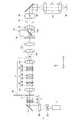
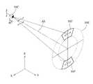
図1は、本発明の実施形態にかかる照明光学装置を備えた露光装置の構成を概略的に示す図である。図1において、感光性基板であるウェハWの法線方向に沿ってZ軸を、ウェハWの面内において図1の紙面に平行な方向にY軸を、ウェハWの面内において図1の紙面に垂直な方向にX軸をそれぞれ設定している。本実施形態の露光装置は、露光光(照明光)を供給するための光源1を備えている。 FIG. 1 is a view schematically showing a configuration of an exposure apparatus provided with an illumination optical apparatus according to an embodiment of the present invention. In FIG. 1, the Z axis along the normal direction of the wafer W, which is a photosensitive substrate, the Y axis in the direction parallel to the plane of FIG. 1 in the plane of the wafer W, and the plane of the wafer W in FIG. The X axis is set in the direction perpendicular to the paper surface. The exposure apparatus of this embodiment includes a light source 1 for supplying exposure light (illumination light).
光源1として、たとえば248nmの波長の光を供給するKrFエキシマレーザ光源や193nmの波長の光を供給するArFエキシマレーザ光源などを用いることができる。光源1からZ方向に沿って射出されたほぼ平行な光束は、X方向に沿って細長く延びた矩形状の断面を有し、一対のレンズ2aおよび2bからなるビームエキスパンダー2に入射する。各レンズ2aおよび2bは、図1の紙面内(YZ平面内)において負の屈折力および正の屈折力をそれぞれ有する。したがって、ビームエキスパンダー2に入射した光束は、図1の紙面内において拡大され、所定の矩形状の断面を有する光束に整形される。 As the light source 1, for example, a KrF excimer laser light source that supplies light with a wavelength of 248 nm, an ArF excimer laser light source that supplies light with a wavelength of 193 nm, or the like can be used. A substantially parallel light beam emitted from the light source 1 along the Z direction has a rectangular cross section extending along the X direction and is incident on the beam expander 2 including a pair of
整形光学系としてのビームエキスパンダー2を介したほぼ平行な光束は、折り曲げミラー3でY方向に偏向された後、1/4波長板4a、1/2波長板4b、デポラライザ(非偏光化素子)4c、および輪帯照明用の回折光学素子5を介して、アフォーカルレンズ6に入射する。ここで、1/4波長板4a、1/2波長板4b、およびデポラライザ4cは、後述するように、偏光状態切換手段4を構成している。アフォーカルレンズ6は、その前側焦点位置と回折光学素子5の位置とがほぼ一致し且つその後側焦点位置と図中破線で示す所定面7の位置とがほぼ一致するように設定されたアフォーカル系(無焦点光学系)である。 A substantially parallel light beam through a beam expander 2 as a shaping optical system is deflected in the Y direction by a bending mirror 3, and then a
一般に、回折光学素子は、基板に露光光(照明光)の波長程度のピッチを有する段差を形成することによって構成され、入射ビームを所望の角度に回折する作用を有する。具体的には、輪帯照明用の回折光学素子5は、矩形状の断面を有する平行光束が入射した場合に、そのファーフィールド(またはフラウンホーファー回折領域)に輪帯状の光強度分布を形成する機能を有する。したがって、光束変換素子としての回折光学素子5に入射したほぼ平行光束は、アフォーカルレンズ6の瞳面に輪帯状の光強度分布を形成した後、ほぼ平行光束となってアフォーカルレンズ6から射出される。 In general, a diffractive optical element is formed by forming a step having a pitch of the wavelength of exposure light (illumination light) on a substrate, and has a function of diffracting an incident beam to a desired angle. Specifically, the diffractive optical element 5 for annular illumination forms an annular light intensity distribution in the far field (or Fraunhofer diffraction region) when a parallel light beam having a rectangular cross section is incident. It has a function. Accordingly, the substantially parallel light beam incident on the diffractive optical element 5 as the light beam conversion element forms an annular light intensity distribution on the pupil plane of the afocal lens 6 and then exits from the afocal lens 6 as a substantially parallel light beam. Is done.
なお、アフォーカルレンズ6の前側レンズ群6aと後側レンズ群6bとの間の光路中においてその瞳面またはその近傍には、光源側から順に、円錐アキシコン系8、第1シリンドリカルレンズ対9、および第2シリンドリカルレンズ対10が配置されているが、その詳細な構成および作用については後述する。以下、説明を簡単にするために、円錐アキシコン系8、第1シリンドリカルレンズ対9、および第2シリンドリカルレンズ対10の作用を無視して、基本的な構成および作用を説明する。 In the optical path between the
アフォーカルレンズ6を介した光束は、σ値可変用のズームレンズ11を介して、オプティカルインテグレータとしてのマイクロフライアイレンズ(またはフライアイレンズ)12に入射する。マイクロフライアイレンズ12は、縦横に且つ稠密に配列された多数の正屈折力を有する微小レンズからなる光学素子である。一般に、マイクロフライアイレンズは、たとえば平行平面板にエッチング処理を施して微小レンズ群を形成することによって構成される。 The light beam that has passed through the afocal lens 6 enters a micro fly's eye lens (or fly eye lens) 12 as an optical integrator through a
ここで、マイクロフライアイレンズを構成する各微小レンズは、フライアイレンズを構成する各レンズエレメントよりも微小である。また、マイクロフライアイレンズは、互いに隔絶されたレンズエレメントからなるフライアイレンズとは異なり、多数の微小レンズ(微小屈折面)が互いに隔絶されることなく一体的に形成されている。しかしながら、正屈折力を有するレンズ要素が縦横に配置されている点でマイクロフライアイレンズはフライアイレンズと同じ波面分割型のオプティカルインテグレータである。 Here, each micro lens constituting the micro fly's eye lens is smaller than each lens element constituting the fly eye lens. Further, unlike a fly-eye lens composed of lens elements isolated from each other, a micro fly-eye lens is formed integrally with a large number of micro lenses (micro refractive surfaces) without being isolated from each other. However, the micro fly's eye lens is the same wavefront division type optical integrator as the fly eye lens in that lens elements having positive refractive power are arranged vertically and horizontally.
所定面7の位置はズームレンズ11の前側焦点位置の近傍に配置され、マイクロフライアイレンズ12の入射面はズームレンズ11の後側焦点位置の近傍に配置されている。換言すると、ズームレンズ11は、所定面7とマイクロフライアイレンズ12の入射面とを実質的にフーリエ変換の関係に配置し、ひいてはアフォーカルレンズ6の瞳面とマイクロフライアイレンズ12の入射面とを光学的にほぼ共役に配置している。 The position of the predetermined surface 7 is disposed in the vicinity of the front focal position of the
したがって、マイクロフライアイレンズ12の入射面上には、アフォーカルレンズ6の瞳面と同様に、たとえば光軸AXを中心とした輪帯状の照野が形成される。この輪帯状の照野の全体形状は、ズームレンズ11の焦点距離に依存して相似的に変化する。マイクロフライアイレンズ12を構成する各微小レンズは、マスクM上において形成すべき照野の形状(ひいてはウェハW上において形成すべき露光領域の形状)と相似な矩形状の断面を有する。 Accordingly, on the incident surface of the micro fly's
マイクロフライアイレンズ12に入射した光束は多数の微小レンズにより二次元的に分割され、その後側焦点面(ひいては照明瞳)には、図2に示すように、入射光束によって形成される照野とほぼ同じ光強度分布を有する二次光源、すなわち光軸AXを中心とした輪帯状の実質的な面光源からなる二次光源が形成される。マイクロフライアイレンズ12の後側焦点面に形成された二次光源(一般的には照明光学装置の瞳面またはその近傍に形成された照明瞳分布)からの光束は、ビームスプリッター13aおよびコンデンサー光学系14を介した後、マスクブラインド15を重畳的に照明する。 The light beam incident on the micro fly's
こうして、照明視野絞りとしてのマスクブラインド15には、マイクロフライアイレンズ12を構成する各微小レンズの形状と焦点距離とに応じた矩形状の照野が形成される。なお、ビームスプリッター13aを内蔵する偏光モニター13の内部構成および作用については後述する。マスクブラインド15の矩形状の開口部(光透過部)を介した光束は、結像光学系16の集光作用を受けた後、所定のパターンが形成されたマスクMを重畳的に照明する。 Thus, a rectangular illumination field corresponding to the shape and focal length of each microlens constituting the micro fly's
すなわち、結像光学系16は、マスクブラインド15の矩形状開口部の像をマスクM上に形成することになる。マスクMのパターンを透過した光束は、投影光学系PLを介して、感光性基板であるウェハW上にマスクパターンの像を形成する。こうして、投影光学系PLの光軸AXと直交する平面(XY平面)内においてウェハWを二次元的に駆動制御しながら一括露光またはスキャン露光を行うことにより、ウェハWの各露光領域にはマスクMのパターンが逐次露光される。 That is, the imaging
なお、偏光状態切換手段4において、1/4波長板4aは、光軸AXを中心として結晶光学軸が回転自在に構成されて、入射する楕円偏光の光を直線偏光の光に変換する。また、1/2波長板4bは、光軸AXを中心として結晶光学軸が回転自在に構成されて、入射する直線偏光の偏光面を変化させる。また、デポラライザ4cは、相補的な形状を有する楔形状の水晶プリズム(不図示)と楔形状の石英プリズム(不図示)とにより構成されている。水晶プリズムと石英プリズムとは、一体的なプリズム組立体として、照明光路に対して挿脱自在に構成されている。 In the polarization state switching means 4, the
光源1としてKrFエキシマレーザ光源やArFエキシマレーザ光源を用いる場合、これらの光源から射出される光は典型的には95%以上の偏光度を有し、1/4波長板4aにはほぼ直線偏光の光が入射する。しかしながら、光源1と偏光状態切換手段4との間の光路中に裏面反射鏡としての直角プリズムが介在する場合、入射する直線偏光の偏光面がP偏光面またはS偏光面に一致していないと、直角プリズムでの全反射により直線偏光が楕円偏光に変わる。 When a KrF excimer laser light source or an ArF excimer laser light source is used as the light source 1, the light emitted from these light sources typically has a polarization degree of 95% or more, and the quarter-
偏光状態切換手段4では、たとえば直角プリズムでの全反射に起因して楕円偏光の光が入射しても、1/4波長板4aの作用により変換された直線偏光の光が1/2波長板4bに入射する。1/2波長板4bの結晶光学軸が入射する直線偏光の偏光面に対して0度または90度の角度をなすように設定された場合、1/2波長板4bに入射した直線偏光の光は偏光面が変化することなくそのまま通過する。 In the polarization state switching means 4, for example, even if elliptically polarized light is incident due to total reflection by a right-angle prism, the linearly polarized light converted by the action of the
また、1/2波長板4bの結晶光学軸が入射する直線偏光の偏光面に対して45度の角度をなすように設定された場合、1/2波長板4bに入射した直線偏光の光は偏光面が90度だけ変化した直線偏光の光に変換される。さらに、デポラライザ4cの水晶プリズムの結晶光学軸が入射する直線偏光の偏光面に対して45度の角度をなすように設定された場合、水晶プリズムに入射した直線偏光の光は非偏光状態の光に変換(非偏光化)される。 In addition, when the crystal optical axis of the half-
偏光状態切換手段4では、デポラライザ4cが照明光路中に位置決めされたときに水晶プリズムの結晶光学軸が入射する直線偏光の偏光面に対して45度の角度をなすように構成されている。ちなみに、水晶プリズムの結晶光学軸が入射する直線偏光の偏光面に対して0度または90度の角度をなすように設定された場合、水晶プリズムに入射した直線偏光の光は偏光面が変化することなくそのまま通過する。また、1/2波長板4bの結晶光学軸が入射する直線偏光の偏光面に対して22.5度の角度をなすように設定された場合、1/2波長板4bに入射した直線偏光の光は、偏光面が変化することなくそのまま通過する直線偏光成分と偏光面が90度だけ変化した直線偏光成分とを含む非偏光状態の光に変換される。 The polarization state switching means 4 is configured such that when the
偏光状態切換手段4では、上述したように、直線偏光の光が1/2波長板4bに入射するが、以下の説明を簡単にするために、図1においてZ方向に偏光方向(電場の方向)を有する直線偏光(以下、「Z方向偏光」と称する)の光が1/2波長板4bに入射するものとする。デポラライザ4cを照明光路中に位置決めした場合、1/2波長板4bの結晶光学軸を入射するZ方向偏光の偏光面(偏光方向)に対して0度または90度の角度をなすように設定すると、1/2波長板4bに入射したZ方向偏光の光は偏光面が変化することなくZ方向偏光のまま通過してデポラライザ4cの水晶プリズムに入射する。水晶プリズムの結晶光学軸は入射するZ方向偏光の偏光面に対して45度の角度をなすように設定されているので、水晶プリズムに入射したZ方向偏光の光は非偏光状態の光に変換される。 In the polarization state switching means 4, as described above, linearly polarized light is incident on the half-
水晶プリズムを介して非偏光化された光は、光の進行方向を補償するためのコンペンセータとしての石英プリズムを介して、非偏光状態で回折光学素子5に入射する。一方、1/2波長板4bの結晶光学軸を入射するZ方向偏光の偏光面に対して45度の角度をなすように設定すると、1/2波長板4bに入射したZ方向偏光の光は偏光面が90度だけ変化し、図1においてX方向に偏光方向(電場の方向)を有する直線偏光(以下、「X方向偏光」と称する)の光になってデポラライザ4cの水晶プリズムに入射する。水晶プリズムの結晶光学軸は入射するX方向偏光の偏光面に対しても45度の角度をなすように設定されているので、水晶プリズムに入射したX方向偏光の光は非偏光状態の光に変換され、石英プリズムを介して、非偏光状態で回折光学素子5に入射する。 The light depolarized through the quartz prism enters the diffractive optical element 5 in a non-polarized state through the quartz prism as a compensator for compensating the light traveling direction. On the other hand, when the crystal optical axis of the half-
これに対し、デポラライザ4cを照明光路から退避させた場合、1/2波長板4bの結晶光学軸を入射するZ方向偏光の偏光面に対して0度または90度の角度をなすように設定すると、1/2波長板4bに入射したZ方向偏光の光は偏光面が変化することなくZ方向偏光のまま通過し、Z方向偏光状態で回折光学素子5に入射する。一方、1/2波長板4bの結晶光学軸を入射するZ方向偏光の偏光面に対して45度の角度をなすように設定すると、1/2波長板4bに入射したZ方向偏光の光は偏光面が90度だけ変化してX方向偏光の光になり、X方向偏光状態で回折光学素子5に入射する。 On the other hand, when the
以上のように、偏光状態切換手段4では、デポラライザ4cを照明光路中に挿入して位置決めすることにより、非偏光状態の光を回折光学素子5に入射させることができる。また、デポラライザ4cを照明光路から退避させ且つ1/2波長板4bの結晶光学軸を入射するZ方向偏光の偏光面に対して0度または90度の角度をなすように設定することにより、Z方向偏光状態の光を回折光学素子5に入射させることができる。さらに、デポラライザ4cを照明光路から退避させ且つ1/2波長板4bの結晶光学軸を入射するZ方向偏光の偏光面に対して45度をなすように設定することにより、X方向偏光状態の光を回折光学素子5に入射させることができる。 As described above, in the polarization state switching unit 4, the non-polarized light can be incident on the diffractive optical element 5 by inserting and positioning the
換言すれば、偏光状態切換手段4では、1/4波長板4aと1/2波長板4bとデポラライザ4cとからなる偏光状態切換手段の作用により、回折光学素子5への入射光の偏光状態(後述する本発明にかかる周方向偏光輪帯照明用の回折光学素子以外の通常の回折光学素子を用いている場合にはマスクMおよびウェハWを照明する光の偏光状態)を直線偏光状態と非偏光状態との間で切り換えることができ、直線偏光状態の場合には互いに直交する偏光状態間(Z方向偏光とX方向偏光との間)で切り換えることができる。 In other words, in the polarization state switching means 4, the polarization state of incident light to the diffractive optical element 5 (by the action of the polarization state switching means comprising the
図3は、図1においてアフォーカルレンズの前側レンズ群と後側レンズ群との間の光路中に配置された円錐アキシコン系の構成を概略的に示す図である。円錐アキシコン系8は、光源側から順に、光源側に平面を向け且つマスク側に凹円錐状の屈折面を向けた第1プリズム部材8aと、マスク側に平面を向け且つ光源側に凸円錐状の屈折面を向けた第2プリズム部材8bとから構成されている。 FIG. 3 is a diagram schematically showing the configuration of a conical axicon system disposed in the optical path between the front lens group and the rear lens group of the afocal lens in FIG. The
そして、第1プリズム部材8aの凹円錐状の屈折面と第2プリズム部材8bの凸円錐状の屈折面とは、互いに当接可能なように相補的に形成されている。また、第1プリズム部材8aおよび第2プリズム部材8bのうち少なくとも一方の部材が光軸AXに沿って移動可能に構成され、第1プリズム部材8aの凹円錐状の屈折面と第2プリズム部材8bの凸円錐状の屈折面との間隔が可変に構成されている。 The concave conical refracting surface of the
ここで、第1プリズム部材8aの凹円錐状屈折面と第2プリズム部材8bの凸円錐状屈折面とが互いに当接している状態では、円錐アキシコン系8は平行平面板として機能し、形成される輪帯状の二次光源に及ぼす影響はない。しかしながら、第1プリズム部材8aの凹円錐状屈折面と第2プリズム部材8bの凸円錐状屈折面とを離間させると、円錐アキシコン系8は、いわゆるビームエキスパンダーとして機能する。したがって、円錐アキシコン系8の間隔の変化に伴って、所定面7への入射光束の角度は変化する。 Here, in a state where the concave conical refracting surface of the
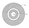
図4は、輪帯状の二次光源に対する円錐アキシコン系の作用を説明する図である。図4を参照すると、円錐アキシコン系8の間隔が零で且つズームレンズ11の焦点距離が最小値に設定された状態(以下、「標準状態」という)で形成された最も小さい輪帯状の二次光源30aが、円錐アキシコン系8の間隔を零から所定の値まで拡大させることにより、その幅(外径と内径との差の1/2:図中矢印で示す)が変化することなく、その外径および内径がともに拡大された輪帯状の二次光源30bに変化する。換言すると、円錐アキシコン系8の作用により、輪帯状の二次光源の幅が変化することなく、その輪帯比(内径/外径)および大きさ(外径)がともに変化する。 FIG. 4 is a diagram for explaining the action of the conical axicon system on the annular secondary light source. Referring to FIG. 4, the smallest annular zone-shaped secondary formed in a state where the distance between the
図5は、輪帯状の二次光源に対するズームレンズの作用を説明する図である。図5を参照すると、標準状態で形成された輪帯状の二次光源30aが、ズームレンズ11の焦点距離を最小値から所定の値へ拡大させることにより、その全体形状が相似的に拡大された輪帯状の二次光源30cに変化する。換言すると、ズームレンズ11の作用により、輪帯状の二次光源の輪帯比が変化することなく、その幅および大きさ(外径)がともに変化する。 FIG. 5 is a diagram illustrating the action of the zoom lens on the annular secondary light source. Referring to FIG. 5, the annular secondary
図6は、図1においてアフォーカルレンズの前側レンズ群と後側レンズ群との間の光路中に配置された第1シリンドリカルレンズ対および第2シリンドリカルレンズ対の構成を概略的に示す図である。図6において、光源側から順に、第1シリンドリカルレンズ対9および第2シリンドリカルレンズ対10が配置されている。第1シリンドリカルレンズ対9は、光源側から順に、たとえばYZ平面内に負屈折力を有し且つXY平面内に無屈折力の第1シリンドリカル負レンズ9aと、同じくYZ平面内に正屈折力を有し且つXY平面内に無屈折力の第1シリンドリカル正レンズ9bとにより構成されている。 FIG. 6 is a diagram schematically showing the configuration of the first cylindrical lens pair and the second cylindrical lens pair arranged in the optical path between the front lens group and the rear lens group of the afocal lens in FIG. . In FIG. 6, a first
一方、第2シリンドリカルレンズ対10は、光源側から順に、たとえばXY平面内に負屈折力を有し且つYZ平面内に無屈折力の第2シリンドリカル負レンズ10aと、同じくXY平面内に正屈折力を有し且つYZ平面内に無屈折力の第2シリンドリカル正レンズ10bとにより構成されている。第1シリンドリカル負レンズ9aと第1シリンドリカル正レンズ9bとは、光軸AXを中心として一体的に回転するように構成されている。同様に、第2シリンドリカル負レンズ10aと第2シリンドリカル正レンズ10bとは、光軸AXを中心として一体的に回転するように構成されている。 On the other hand, the second
こうして、図6に示す状態において、第1シリンドリカルレンズ対9はZ方向にパワーを有するビームエキスパンダーとして機能し、第2シリンドリカルレンズ対10はX方向にパワーを有するビームエキスパンダーとして機能する。なお、第1シリンドリカルレンズ対9のパワーと第2シリンドリカルレンズ対10のパワーとは、互いに同じに設定されている。 Thus, in the state shown in FIG. 6, the first
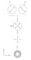
図7〜図9は、輪帯状の二次光源に対する第1シリンドリカルレンズ対および第2シリンドリカルレンズ対の作用を説明する図である。図7では、第1シリンドリカルレンズ対9のパワー方向がZ軸に対して光軸AX廻りに+45度の角度をなし、第2シリンドリカルレンズ対10のパワー方向がZ軸に対して光軸AX廻りに−45度の角度をなすように設定されている。 FIGS. 7 to 9 are diagrams for explaining the action of the first cylindrical lens pair and the second cylindrical lens pair with respect to the annular secondary light source. In FIG. 7, the power direction of the first
したがって、第1シリンドリカルレンズ対9のパワー方向と第2シリンドリカルレンズ対10のパワー方向とが互いに直交し、第1シリンドリカルレンズ対9と第2シリンドリカルレンズ対10との合成系においてZ方向のパワーとX方向のパワーとが互いに同じになる。その結果、図7に示す真円状態では、第1シリンドリカルレンズ対9と第2シリンドリカルレンズ対10との合成系を通過する光束は、Z方向およびX方向に同じパワーで拡大作用を受けることになり、照明瞳には真円輪帯状の二次光源が形成されることになる。 Therefore, the power direction of the first
これに対し、図8では、第1シリンドリカルレンズ対9のパワー方向がZ軸に対して光軸AX廻りに例えば+80度の角度をなし、第2シリンドリカルレンズ対10のパワー方向がZ軸に対して光軸AX廻りに例えば−80度の角度をなすように設定されている。したがって、第1シリンドリカルレンズ対9と第2シリンドリカルレンズ対10との合成系において、Z方向のパワーよりもX方向のパワーの方が大きくなる。その結果、図8に示す横楕円状態では、第1シリンドリカルレンズ対9と第2シリンドリカルレンズ対10との合成系を通過する光束は、Z方向よりもX方向の方が大きなパワーで拡大作用を受けることになり、照明瞳にはX方向に細長い横長の輪帯状の二次光源が形成されることになる。 On the other hand, in FIG. 8, the power direction of the first
一方、図9では、第1シリンドリカルレンズ対9のパワー方向がZ軸に対して光軸AX廻りに例えば+10度の角度をなし、第2シリンドリカルレンズ対10のパワー方向がZ軸に対して光軸AX廻りに例えば−10度の角度をなすように設定されている。したがって、第1シリンドリカルレンズ対9と第2シリンドリカルレンズ対10との合成系において、X方向のパワーよりもZ方向のパワーの方が大きくなる。その結果、図9に示す縦楕円状態では、第1シリンドリカルレンズ対9と第2シリンドリカルレンズ対10との合成系を通過する光束は、X方向よりもZ方向の方が大きなパワーで拡大作用を受けることになり、照明瞳にはZ方向に細長い縦長の輪帯状の二次光源が形成されることになる。 On the other hand, in FIG. 9, the power direction of the first
さらに、第1シリンドリカルレンズ対9および第2シリンドリカルレンズ対10を図7に示す真円状態と図8に示す横楕円状態との間の任意の状態に設定することにより、様々な縦横比にしたがう横長の輪帯状の二次光源を形成することができる。また、第1シリンドリカルレンズ対9および第2シリンドリカルレンズ対10を図7に示す真円状態と図9に示す縦楕円状態との間の任意の状態に設定することにより、様々な縦横比にしたがう縦長の輪帯状の二次光源を形成することができる。 Further, by setting the first
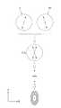
図10は、図1の偏光モニターの内部構成を概略的に示す斜視図である。図10を参照すると、偏光モニター13は、マイクロフライアイレンズ12とコンデンサー光学系14との間の光路中に配置された第1ビームスプリッター13aを備えている。第1ビームスプリッター13aは、たとえば石英ガラスにより形成されたノンコートの平行平面板(すなわち素ガラス)の形態を有し、入射光の偏光状態とは異なる偏光状態の反射光を光路から取り出す機能を有する。 FIG. 10 is a perspective view schematically showing the internal configuration of the polarization monitor of FIG. Referring to FIG. 10, the polarization monitor 13 includes a
第1ビームスプリッター13aにより光路から取り出された光は、第2ビームスプリッター13bに入射する。第2ビームスプリッター13bは、第1ビームスプリッター13aと同様に、例えば石英ガラスにより形成されたノンコートの平行平面板の形態を有し、入射光の偏光状態とは異なる偏光状態の反射光を発生させる機能を有する。そして、第1ビームスプリッター13aに対するP偏光が第2ビームスプリッター13bに対するS偏光になり、且つ第1ビームスプリッター13aに対するS偏光が第2ビームスプリッター13bに対するP偏光になるように設定されている。 The light extracted from the optical path by the
また、第2ビームスプリッター13bを透過した光は第1光強度検出器13cにより検出され、第2ビームスプリッター13bで反射された光は第2光強度検出器13dにより検出される。第1光強度検出器13cおよび第2光強度検出器13dの出力は、それぞれ制御部(不図示)に供給される。制御部は、偏光状態切換手段4を構成する1/4波長板4a、1/2波長板4bおよびデポラライザ4cを必要に応じて駆動する。 The light transmitted through the
上述のように、第1ビームスプリッター13aおよび第2ビームスプリッター13bにおいて、P偏光に対する反射率とS偏光に対する反射率とが実質的に異なっている。したがって、偏光モニター13では、第1ビームスプリッター13aからの反射光が、例えば第1ビームスプリッター13aへの入射光の10%程度のS偏光成分(第1ビームスプリッター13aに対するS偏光成分であって第2ビームスプリッター13bに対するP偏光成分)と、例えば第1ビームスプリッター13aへの入射光の1%程度のP偏光成分(第1ビームスプリッター13aに対するP偏光成分であって第2ビームスプリッター13bに対するS偏光成分)とを含むことになる。 As described above, in the
また、第2ビームスプリッター13bからの反射光は、例えば第1ビームスプリッター13aへの入射光の10%×1%=0.1%程度のP偏光成分(第1ビームスプリッター13aに対するP偏光成分であって第2ビームスプリッター13bに対するS偏光成分)と、例えば第1ビームスプリッター13aへの入射光の1%×10%=0.1%程度のS偏光成分(第1ビームスプリッター13aに対するS偏光成分であって第2ビームスプリッター13bに対するP偏光成分)とを含むことになる。 The reflected light from the
こうして、偏光モニター13では、第1ビームスプリッター13aが、その反射特性に応じて、入射光の偏光状態とは異なる偏光状態の反射光を光路から取り出す機能を有する。その結果、第2ビームスプリッター13bの偏光特性による偏光変動の影響を僅かに受けるものの、第1光強度検出器13cの出力(第2ビームスプリッター13bの透過光の強度に関する情報、すなわち第1ビームスプリッター13aからの反射光とほぼ同じ偏光状態の光の強度に関する情報)に基づいて、第1ビームスプリッター13aへの入射光の偏光状態(偏光度)を、ひいてはマスクMへの照明光の偏光状態を検知することができる。 Thus, in the
また、偏光モニター13では、第1ビームスプリッター13aに対するP偏光が第2ビームスプリッター13bに対するS偏光になり且つ第1ビームスプリッター13aに対するS偏光が第2ビームスプリッター13bに対するP偏光になるように設定されている。その結果、第2光強度検出器13dの出力(第1ビームスプリッター13aおよび第2ビームスプリッター13bで順次反射された光の強度に関する情報)に基づいて、第1ビームスプリッター13aへの入射光の偏光状態の変化の影響を実質的に受けることなく、第1ビームスプリッター13aへの入射光の光量(強度)を、ひいてはマスクMへの照明光の光量を検知することができる。 The polarization monitor 13 is set so that the P-polarized light for the
こうして、偏光モニター13を用いて、第1ビームスプリッター13aへの入射光の偏光状態を検知し、ひいてはマスクMへの照明光が所望の非偏光状態または直線偏光状態になっているか否かを判定することができる。そして、制御部が偏光モニター13の検知結果に基づいてマスクM(ひいてはウェハW)への照明光が所望の非偏光状態または直線偏光状態になっていないことを確認した場合、偏光状態切換手段4を構成する1/4波長板4a、1/2波長板4bおよびデポラライザ4cを駆動調整し、マスクMへの照明光の状態を所望の非偏光状態または直線偏光状態に調整することができる。 In this way, the polarization monitor 13 is used to detect the polarization state of the light incident on the
なお、輪帯照明用の回折光学素子5に代えて、4極照明用の回折光学素子(不図示)を照明光路中に設定することによって、4極照明を行うことができる。4極照明用の回折光学素子は、矩形状の断面を有する平行光束が入射した場合に、そのファーフィールドに4極状の光強度分布を形成する機能を有する。したがって、4極照明用の回折光学素子を介した光束は、マイクロフライアイレンズ12の入射面に、たとえば光軸AXを中心とした4つの円形状の照野からなる4極状の照野を形成する。その結果、マイクロフライアイレンズ12の後側焦点面にも、その入射面に形成された照野と同じ4極状の二次光源が形成される。 In addition, instead of the diffractive optical element 5 for annular illumination, quadrupole illumination can be performed by setting a diffractive optical element (not shown) for quadrupole illumination in the illumination optical path. The diffractive optical element for quadrupole illumination has a function of forming a quadrupole light intensity distribution in the far field when a parallel light beam having a rectangular cross section is incident. Therefore, the light beam that has passed through the diffractive optical element for quadrupole illumination has a quadrupole illumination field composed of, for example, four circular illumination fields centered on the optical axis AX on the incident surface of the micro fly's
また、輪帯照明用の回折光学素子5に代えて、円形照明用の回折光学素子(不図示)を照明光路中に設定することによって、通常の円形照明を行うことができる。円形照明用の回折光学素子は、矩形状の断面を有する平行光束が入射した場合に、ファーフィールドに円形状の光強度分布を形成する機能を有する。したがって、円形照明用の回折光学素子を介した光束は、マイクロフライアイレンズ12の入射面に、たとえば光軸AXを中心とした円形状の照野からなる4極状の照野を形成する。その結果、マイクロフライアイレンズ12の後側焦点面にも、その入射面に形成された照野と同じ円形状の二次光源が形成される。 Moreover, instead of the diffractive optical element 5 for annular illumination, normal circular illumination can be performed by setting a diffractive optical element (not shown) for circular illumination in the illumination optical path. The diffractive optical element for circular illumination has a function of forming a circular light intensity distribution in the far field when a parallel light beam having a rectangular cross section is incident. Therefore, the light beam that has passed through the diffractive optical element for circular illumination forms a quadrupole illumination field on the incident surface of the micro fly's
さらに、輪帯照明用の回折光学素子5に代えて、他の複数極照明用の回折光学素子(不図示)を照明光路中に設定することによって、様々な複数極照明(2極照明、8極照明など)を行うことができる。同様に、輪帯照明用の回折光学素子5に代えて、適当な特性を有する回折光学素子(不図示)を照明光路中に設定することによって、様々な形態の変形照明を行うことができる。 Furthermore, by replacing the diffractive optical element 5 for annular illumination with another diffractive optical element (not shown) for multi-pole illumination in the illumination optical path, various multi-pole illumination (bi-polar illumination, 8 Polar lighting etc.). Similarly, various forms of modified illumination can be performed by setting a diffractive optical element (not shown) having appropriate characteristics in the illumination optical path instead of the diffractive optical element 5 for annular illumination.
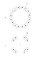
本実施形態では、輪帯照明用の回折光学素子5に代えて、いわゆる周方向偏光輪帯照明用の回折光学素子50を照明光路中に設定することによって、輪帯状の二次光源を通過する光束が周方向偏光状態に設定された変形照明、すなわち周方向偏光輪帯照明を行うことができる。図11は、本実施形態にかかる周方向偏光輪帯照明用の回折光学素子の構成を概略的に示す図である。また、図12は、周方向偏光状態に設定された輪帯状の二次光源を概略的に示す図である。 In this embodiment, instead of the diffractive optical element 5 for annular illumination, a so-called circumferential polarization annular illumination diffractive
図11および図12を参照すると、本実施形態にかかる周方向偏光輪帯照明用の回折光学素子50は、互いに同じ矩形状の断面を有し且つ光の透過方向(Y方向)に沿った厚さ(光軸方向の長さ)が互いに異なる4種類の基本素子50A〜50Dを縦横に且つ稠密に配置することにより構成されている。ここで、第1基本素子50Aの厚さが最も大きく、第4基本素子50Dの厚さが最も小さく、第2基本素子50Bの厚さは第3基本素子50Cの厚さよりも大きく設定されている。 Referring to FIGS. 11 and 12, the diffractive
また、回折光学素子50は、第1基本素子50Aと第2基本素子50Bと第3基本素子50Cと第4基本素子50Dとをほぼ同数含み、4種類の基本素子50A〜50Dはほぼランダム配置されている。さらに、各基本素子50A〜50Dのマスク側には回折面(図中斜線部で示す)が形成され、各基本素子50A〜50Dの回折面が光軸AX(図11では不図示)と直交する1つの平面に沿うように整列されている。その結果、回折光学素子50のマスク側の面は平面状であるが、回折光学素子50の光源側の面は各基本素子50A〜50Dの厚さの違いにより凹凸状になっている。 The diffractive
そして、第1基本素子50Aの回折面は、図12に示す輪帯状の二次光源31のうち、光軸AXを通るZ方向の軸線に関して対称的な一対の円弧状領域31Aを形成するように構成されている。すなわち、図13に示すように、第1基本素子50Aは、回折光学素子50のファーフィールド(ひいては各基本素子50A〜50Dのファーフィールド)50Eに光軸AXを通るZ方向の軸線に関して対称的な一対の円弧状の光強度分布32A(一対の円弧状領域31Aに対応)を形成する機能を有する。 The diffractive surface of the first
第2基本素子50Bの回折面は、光軸AXを通るZ方向の軸線をY軸廻りに−45度回転させた(図12中反時計回りに45度回転させた)軸線に関して対称的な一対の円弧状領域31Bを形成するように構成されている。すなわち、図14に示すように、第2基本素子50Bは、ファーフィールド50Eに、光軸AXを通るZ方向の軸線をY軸廻りに−45度回転させた軸線に関して対称的な一対の円弧状の光強度分布32B(一対の円弧状領域31Bに対応)を形成する機能を有する。 The diffractive surface of the second
第3基本素子50Cの回折面は、光軸AXを通るX方向の軸線に関して対称的な一対の円弧状領域31Cを形成するように構成されている。すなわち、図15に示すように、第3基本素子50Cは、ファーフィールド50Eに、光軸AXを通るX方向の軸線に関して対称的な一対の円弧状の光強度分布32C(一対の円弧状領域31Cに対応)を形成する機能を有する。 The diffractive surface of the third
第4基本素子50Dの回折面は、光軸AXを通るZ方向の軸線をY軸廻りに+45度回転させた(図12中時計回りに45度回転させた)軸線に関して対称的な一対の円弧状領域31Dを形成するように構成されている。すなわち、図16に示すように、第4基本素子50Dは、ファーフィールド50Eに、光軸AXを通るZ方向の軸線をY軸廻りに+45度回転させた軸線に関して対称的な一対の円弧状の光強度分布32D(一対の円弧状領域31Dに対応)を形成する機能を有する。なお、各円弧状領域31A〜31Dの大きさは互いにほぼ等しく、8つの円弧状領域31A〜31Dが互いに重複することなく且つ互いに離間することなく、光軸AXを中心とした輪帯状の二次光源31を構成している。 The diffractive surface of the fourth
また、本実施形態では、各基本素子50A〜50Dが旋光性を有する光学材料である水晶により構成され、各基本素子50A〜50Dの結晶光学軸が光軸AXとほぼ一致するように設定されている。以下、図17を参照して、水晶の旋光性について簡単に説明する。図17を参照すると、厚さdの水晶からなる平行平面板状の光学部材35が、その結晶光学軸と光軸AXとが一致するように配置されている。この場合、光学部材35の旋光性により、入射した直線偏光の偏光方向が光軸AX廻りにθだけ回転した状態で射出される。 In the present embodiment, each of the
このとき、光学部材35の旋光性による偏光方向の回転角θは、光学部材35の厚さdと水晶の旋光能ρとにより、次の式(1)で表わされる。 At this time, the rotation angle θ in the polarization direction due to the optical rotation of the
θ=d・ρ (1)
一般に、水晶の旋光能ρは使用光の波長が短くなると大きくなる傾向があるが、「応用光学II」の第167頁の記述によれば、250.3nmの波長を有する光に対する水晶の旋光能ρは153.9度/mmである。θ = d · ρ (1)
In general, the optical rotation power ρ of a crystal tends to increase as the wavelength of the used light becomes shorter. ρ is 153.9 degrees / mm.
本実施形態において、第1基本素子50Aは、図13に示すように、Z方向に偏光方向を有する直線偏光の光が入射した場合、Z方向をY軸廻りに+180度回転させた方向すなわちZ方向に偏光方向を有する直線偏光の光を射出するように厚さdAが設定されている。その結果、ファーフィールド50Eに形成される一対の円弧状の光強度分布32Aを通過する光束の偏光方向もZ方向になり、図12に示す一対の円弧状領域31Aを通過する光束の偏光方向もZ方向になる。 In the present embodiment, as shown in FIG. 13, in the first
第2基本素子50Bは、図14に示すように、Z方向に偏光方向を有する直線偏光の光が入射した場合、Z方向をY軸廻りに+135度回転させた方向すなわちZ方向をY軸廻りに−45度回転させた方向に偏光方向を有する直線偏光の光を射出するように厚さdBが設定されている。その結果、ファーフィールド50Eに形成される一対の円弧状の光強度分布32Bを通過する光束の偏光方向もZ方向をY軸廻りに−45度回転させた方向になり、図12に示す一対の円弧状領域31Aを通過する光束の偏光方向もZ方向をY軸廻りに−45度回転させた方向になる。 As shown in FIG. 14, in the second
第3基本素子50Cは、図15に示すように、Z方向に偏光方向を有する直線偏光の光が入射した場合、Z方向をY軸廻りに+90度回転させた方向すなわちX方向に偏光方向を有する直線偏光の光を射出するように厚さdCが設定されている。その結果、ファーフィールド50Eに形成される一対の円弧状の光強度分布32Cを通過する光束の偏光方向もX方向になり、図12に示す一対の円弧状領域31Cを通過する光束の偏光方向もX方向になる。 As shown in FIG. 15, when the linearly polarized light having the polarization direction in the Z direction is incident, the third
第4基本素子50Dは、図16に示すように、Z方向に偏光方向を有する直線偏光の光が入射した場合、Z方向をY軸廻りに+45度回転させた方向に偏光方向を有する直線偏光の光を射出するように厚さdDが設定されている。その結果、ファーフィールド50Eに形成される一対の円弧状の光強度分布32Dを通過する光束の偏光方向もZ方向をY軸廻りに+45度回転させた方向になり、図12に示す一対の円弧状領域31Dを通過する光束の偏光方向もZ方向をY軸廻りに+45度回転させた方向になる。 As shown in FIG. 16, in the fourth
本実施形態では、周方向偏光輪帯照明に際して、周方向偏光輪帯照明用の回折光学素子50を照明光路中に設定し、Z方向に偏光方向を有する直線偏光の光を回折光学素子50に入射させる。その結果、マイクロフライアイレンズ12の後側焦点面(すなわち照明瞳またはその近傍)には、図12に示すように、輪帯状の二次光源(輪帯状の照明瞳分布)31が形成され、この輪帯状の二次光源31を通過する光束が周方向偏光状態に設定される。 In the present embodiment, during circumferential polarization annular illumination, a diffractive
周方向偏光状態では、輪帯状の二次光源31を構成する円弧状領域31A〜31Dをそれぞれ通過する光束は、各円弧状領域31A〜31Dの円周方向に沿った中心位置における光軸AXを中心とする円の接線とほぼ一致する偏光方向を有する直線偏光状態になる。 In the circumferential polarization state, the light beams passing through the arc-shaped
このように本実施形態では、入射光束に基づいて所定面に所定の光強度分布を形成するための光束変換素子50が、旋光性を有する光学材料により形成されて、前記入射光束に基づいて前記所定の光強度分布のうちの第1領域分布32Aを形成するための第1基本素子50Aと;旋光性を有する光学材料により形成されて、前記入射光束に基づいて前記所定の光強度分布のうちの第2領域分布32Bを形成するための第2基本素子50Bとを備えており、第1基本素子50Aと第2基本素子50Bとの光の透過方向に沿った厚さが互いに異なっている。 As described above, in the present embodiment, the light
このような構成により、本実施形態では、開口絞りにおいて大きな光量損失が発生する従来技術とは異なり、光束変換素子としての回折光学素子50の回折作用と旋光作用とにより、光量損失を実質的に発生させることなく、周方向偏光状態の輪帯状の二次光源31を形成することができる。 With such a configuration, in the present embodiment, unlike the conventional technique in which a large light amount loss occurs in the aperture stop, the light amount loss is substantially reduced by the diffractive action and the optical rotatory action of the diffractive
ここで、本実施形態の好ましい態様によれば、第1基本素子50Aの厚さおよび第2基本素子50Bの厚さは、直線偏光が入射したときに第1領域分布32Aを形成する直線偏光の偏光方向と第2領域分布32Bを形成する直線偏光の偏光方向とが異なるように設定されている。また、第1領域分布32Aおよび第2領域分布32Bは、所定面における所定点を中心とする所定の輪帯領域である所定輪帯領域の少なくとも一部に位置決めされ、第1領域分布32Aおよび第2領域分布32Bを通過する光束は、所定輪帯領域の円周方向を偏光方向とする直線偏光を主成分とする偏光状態を有することが好ましい。 Here, according to a preferred aspect of the present embodiment, the thickness of the first
この場合、所定の光強度分布は、所定輪帯領域とほぼ同一形状の外形を有し、第1領域分布32Aを通過する光束の偏光状態は、第1領域分布32Aの円周方向に沿った中心位置における所定点を中心とする円の接線方向とほぼ一致した直線偏光成分を有し、第2領域分布32Bを通過する光束の偏光状態は、第2領域分布32Bの円周方向に沿った中心位置における所定点を中心とする円の接線方向とほぼ一致した直線偏光成分を有することが好ましい。あるいは、所定の光強度分布は、所定輪帯領域内に分布する多極状であり、第1領域分布を通過する光束の偏光状態は、第1領域分布の円周方向に沿った中心位置における所定点を中心とする円の接線方向とほぼ一致した直線偏光成分を有し、第2領域分布を通過する光束の偏光状態は、第2領域分布の円周方向に沿った中心位置における所定点を中心とする円の接線方向とほぼ一致した直線偏光成分を有することが好ましい。 In this case, the predetermined light intensity distribution has substantially the same shape as that of the predetermined ring zone region, and the polarization state of the light beam passing through the
また、本実施形態の好ましい態様によれば、第1基本素子および第2基本素子は、使用波長の光に対して100度/mm以上の旋光能を有する光学材料により形成されている。また、第1基本素子および第2基本素子は、水晶により形成されていることが好ましい。また、光束変換素子は、第1基本素子と第2基本素子とをほぼ同数含むことが好ましい。また、第1基本素子および第2基本素子は、回折作用または屈折作用を有することが好ましい。 Further, according to a preferred aspect of the present embodiment, the first basic element and the second basic element are formed of an optical material having an optical rotation power of 100 degrees / mm or more with respect to light of the wavelength used. The first basic element and the second basic element are preferably formed of quartz. Moreover, it is preferable that the light beam conversion element includes substantially the same number of first basic elements and second basic elements. The first basic element and the second basic element preferably have a diffractive action or a refractive action.
また、本実施形態の好ましい態様によれば、第1基本素子は、入射光束に基づいて少なくとも2つの第1領域分布を所定面上に形成し、第2基本素子は、入射光束に基づいて少なくとも2つの第2領域分布を所定面上に形成することが好ましい。また、旋光性を有する光学材料により形成されて、入射光束に基づいて所定の光強度分布のうちの第3領域分布32Cを形成するための第3基本素子50Cと、旋光性を有する光学材料により形成されて、入射光束に基づいて所定の光強度分布のうちの第4領域分布32Dを形成するための第4基本素子50Dとをさらに備えていることが好ましい。 According to a preferred aspect of the present embodiment, the first basic element forms at least two first region distributions on a predetermined plane based on the incident light beam, and the second basic element is at least based on the incident light beam. It is preferable to form two second region distributions on a predetermined surface. Further, the third
また、本実施形態では、入射光束に基づいて、該入射光束の断面形状とは異なる形状の所定の光強度分布を所定面上に形成するための光束変換素子50が、所定面上に所定の光強度分布を形成するための、回折面または屈折面を備え、所定の光強度分布は、所定面における所定点を中心とする所定の輪帯領域である所定輪帯領域の少なくとも一部に分布し、所定輪帯領域を通過する光束変換素子からの光束は、所定輪帯領域の円周方向を偏光方向とする直線偏光を主成分とする偏光状態を有している。 In the present embodiment, the light
このような構成により、本実施形態では、開口絞りにおいて大きな光量損失が発生する従来技術とは異なり、光束変換素子としての回折光学素子50の回折作用と旋光作用とにより、光量損失を実質的に発生させることなく、周方向偏光状態の輪帯状の二次光源31を形成することができる。 With such a configuration, in the present embodiment, unlike the conventional technique in which a large light amount loss occurs in the aperture stop, the light amount loss is substantially reduced by the diffractive action and the optical rotatory action of the diffractive
本実施形態の好ましい態様によれば、所定の光強度分布は、多極形状または輪帯状の外形を有する。また、光束変換素子は、旋光性を有する光学材料により形成されることが好ましい。 According to a preferred aspect of the present embodiment, the predetermined light intensity distribution has a multipolar shape or an annular shape. The light beam conversion element is preferably formed of an optical material having optical activity.
また、本実施形態の照明光学装置は、光源からの光束に基づいて被照射面を照明する照明光学装置であって、照明光学装置の照明瞳またはその近傍に照明瞳分布を形成するために光源からの光束を変換するために上述の光束変換素子を備えている。このような構成により、本実施形態の照明光学装置では、光量損失を良好に抑えつつ、周方向偏光状態の輪帯状の照明瞳分布を形成することができる。 The illumination optical device according to the present embodiment is an illumination optical device that illuminates a surface to be irradiated based on a light beam from a light source, and the light source is used to form an illumination pupil distribution at or near the illumination pupil of the illumination optical device. Is provided with the above-described light beam conversion element. With such a configuration, the illumination optical device of the present embodiment can form a ring-shaped illumination pupil distribution in a circumferentially polarized state while suppressing a light amount loss satisfactorily.
ここで、光束変換素子は、特性の異なる他の光束変換素子と交換可能に構成されていることが好ましい。また、光束変換素子と被照射面との間の光路中に配置された波面分割型のオプティカルインテグレータをさらに備え、光束変換素子は、入射光束に基づいてオプティカルインテグレータの入射面に所定の光強度分布を形成することが好ましい。 Here, the light beam conversion element is preferably configured to be exchangeable with other light beam conversion elements having different characteristics. The optical system further includes a wavefront splitting type optical integrator disposed in the optical path between the light beam conversion element and the irradiated surface, and the light beam conversion element has a predetermined light intensity distribution on the incident surface of the optical integrator based on the incident light beam. Is preferably formed.
また、本実施形態の照明光学装置の好ましい態様によれば、所定面上の光強度分布と、所定輪帯領域を通過する光束変換素子からの光束の偏光状態との少なくとも何れか一方は、光源と被照射面との間の光路中に配置される光学部材による影響を考慮して設定される。また、光束変換素子からの光束の偏光状態を、被照射面に照射される光がS偏光を主成分とする偏光状態となるように設定することが好ましい。 According to a preferred aspect of the illumination optical apparatus of the present embodiment, at least one of the light intensity distribution on the predetermined surface and the polarization state of the light beam from the light beam conversion element passing through the predetermined ring zone region is a light source. Is set in consideration of the influence of the optical member disposed in the optical path between the surface and the irradiated surface. Moreover, it is preferable to set the polarization state of the light beam from the light beam conversion element so that the light irradiated on the irradiated surface is in a polarization state mainly composed of S-polarized light.
また、本実施形態の露光装置は、マスクを照明するための上述の照明光学装置を備え、マスクのパターンを感光性基板上に露光する。ここで、所定面上の光強度分布と、所定輪帯領域を通過する光束変換素子からの光束の偏光状態との少なくとも何れか一方は、光源と感光性基板との間の光路中に配置される光学部材による影響を考慮して設定されることが好ましい。また、光束変換素子からの光束の偏光状態を、感光性基板に照射される光がS偏光を主成分とする偏光状態となるように設定することが好ましい。 Moreover, the exposure apparatus of this embodiment is provided with the above-mentioned illumination optical apparatus for illuminating a mask, and exposes the pattern of a mask on a photosensitive substrate. Here, at least one of the light intensity distribution on the predetermined surface and the polarization state of the light beam from the light beam conversion element passing through the predetermined ring zone region is disposed in the optical path between the light source and the photosensitive substrate. It is preferable to set in consideration of the influence of the optical member. Moreover, it is preferable to set the polarization state of the light beam from the light beam conversion element so that the light irradiated to the photosensitive substrate is in a polarization state mainly composed of S-polarized light.
また、本実施形態の露光方法では、上述の照明光学装置を用いてマスクを照明する照明工程と、マスクのパターンを感光性基板上に露光する露光工程とを含んでいる。ここで、所定面上の光強度分布と、所定輪帯領域を通過する光束変換素子からの光束の偏光状態との少なくとも何れか一方は、光源と感光性基板との間の光路中に配置される光学部材による影響を考慮して設定されることが好ましい。また、光束変換素子からの光束の偏光状態を、感光性基板に照射される光がS偏光を主成分とする偏光状態となるように設定することが好ましい。 Further, the exposure method of the present embodiment includes an illumination process for illuminating the mask using the above-described illumination optical device, and an exposure process for exposing the pattern of the mask onto the photosensitive substrate. Here, at least one of the light intensity distribution on the predetermined surface and the polarization state of the light beam from the light beam conversion element passing through the predetermined ring zone region is disposed in the optical path between the light source and the photosensitive substrate. It is preferable to set in consideration of the influence of the optical member. Moreover, it is preferable to set the polarization state of the light beam from the light beam conversion element so that the light irradiated to the photosensitive substrate is in a polarization state mainly composed of S-polarized light.
換言すれば、本実施形態の照明光学装置では、光量損失を良好に抑えつつ、周方向偏光状態の輪帯状の照明瞳分布を形成することができる。その結果、本実施形態の露光装置では、光量損失を良好に抑えつつ周方向偏光状態の輪帯状の照明瞳分布を形成することのできる照明光学装置を用いているので、適切な照明条件のもとで任意方向の微細パターンを忠実に且つ高スループットで転写することができる。 In other words, in the illumination optical device according to the present embodiment, it is possible to form a ring-shaped illumination pupil distribution in a circumferentially polarized state while suppressing light amount loss satisfactorily. As a result, the exposure apparatus of the present embodiment uses an illumination optical apparatus that can form a ring-shaped illumination pupil distribution in a circumferentially polarized state while suppressing the light amount loss satisfactorily. Thus, a fine pattern in any direction can be transferred faithfully and with high throughput.
なお、周方向偏光状態の輪帯状の照明瞳分布に基づく周方向偏光輪帯照明では、被照射面としてのウェハWに照射される光がS偏光を主成分とする偏光状態になる。ここで、S偏光とは、入射面に対して垂直な方向に偏光方向を持つ直線偏光(入射面に垂直な方向に電気ベクトルが振動している偏光)のことである。ただし、入射面とは、光が媒質の境界面(被照射面:ウェハWの表面)に達したときに、その点での境界面の法線と光の入射方向とを含む面として定義される。 In the circumferential polarization annular illumination based on the annular illumination pupil distribution in the circumferential polarization state, the light irradiated on the wafer W as the irradiated surface is in a polarization state mainly composed of S-polarized light. Here, S-polarized light is linearly polarized light having a polarization direction in a direction perpendicular to the incident surface (polarized light having an electric vector oscillating in a direction perpendicular to the incident surface). However, the incident surface is defined as a surface including the normal of the boundary surface at that point and the incident direction of light when the light reaches the boundary surface of the medium (surface to be irradiated: the surface of the wafer W). The
なお、上述の実施形態では、互いに同じ矩形状の断面を有する4種類の基本素子50A〜50Dをほぼ同数だけ縦横に且つ稠密にランダム配置することにより、周方向偏光輪帯照明用の回折光学素子50を構成している。しかしながら、これに限定されることなく、各基本素子の数、断面形状、種類数、配置などについて様々な変形例が可能である。 In the above-described embodiment, four types of
また、上述の実施形態では、4種類の基本素子50A〜50Dからなる回折光学素子50を用いて、互いに重複することなく且つ互いに離間することなく配列された8つの円弧状領域31A〜31Dにより、光軸AXを中心とした輪帯状の二次光源31を構成している。しかしながら、これに限定されることなく、輪帯状の二次光源を構成する領域の数、形状、配置などについて様々な変形例が可能である。 Further, in the above-described embodiment, by using the diffractive
具体的には、図18(a)に示すように、たとえば4種類の基本素子からなる回折光学素子を用いて、周方向に沿って互いに離間した8つの円弧状領域からなる周方向偏光状態の8極状の二次光源33aを形成することもできる。また、図18(b)に示すように、たとえば4種類の基本素子からなる回折光学素子を用いて、周方向に沿って互いに離間した4つの円弧状領域からなる周方向偏光状態の4極状の二次光源33bを形成することもできる。なお、これらの8極状の二次光源または4極状の二次光源において、各領域の形状は円弧状に限定されることなく、たとえば円形状や楕円状や扇形状であってもよい。また、図19に示すように、たとえば4種類の基本素子からなる回折光学素子を用いて、周方向に沿って互いに重複した8つの円弧状領域からなる周方向偏光状態の輪帯状の二次光源33cを形成することもできる。 Specifically, as shown in FIG. 18A, for example, by using a diffractive optical element composed of four types of basic elements, a circumferential polarization state composed of eight arc-shaped regions separated from each other along the circumferential direction. An octupole secondary
また、周方向に沿って互いに離間した4つまたは8つの領域からなる周方向偏光状態の4極状または8極状の二次光源の他に、図20(a)に示すように、周方向に沿って互いに離間した6つの領域からなる周方向偏光状態の6極状の二次光源を形成しても良い。また、図20(b)に示すように、周方向に沿って互いに離間した複数の領域からなる周方向偏光状態の多極状の二次光源と、光軸上の領域からなる非偏光状態または直線偏光状態の中心極上の二次光源とを持つ二次光源を形成しても良い。また、周方向に沿って互いに離間した2つの領域からなる周方向偏光状態の2極状の二次光源を形成しても良い。 In addition to a quadrupole or octupole secondary light source having a circumferential polarization state composed of four or eight regions spaced apart from each other along the circumferential direction, as shown in FIG. A hexapolar secondary light source having a circumferential polarization state composed of six regions spaced apart from each other may be formed. In addition, as shown in FIG. 20 (b), a multipolar secondary light source having a circumferential polarization state composed of a plurality of regions spaced apart from each other along the circumferential direction, and a non-polarization state comprising a region on the optical axis or A secondary light source having a secondary light source on the central pole in a linear polarization state may be formed. Moreover, you may form the bipolar secondary light source of the circumferential direction polarization state which consists of two area | regions mutually spaced apart along the circumferential direction.
また、上述の実施形態では、図11に示すように、4種類の基本素子50A〜50Dを個別に形成し、これらの素子を組み合わせることにより回折光学素子50を構成している。しかしながら、これに限定されることなく、1つの水晶基板に対して例えばエッチング加工を施すことにより各基本素子50A〜50Dの射出側の回折面および入射側の凹凸面を形成し、回折光学素子50を一体的に構成することもできる。 In the above-described embodiment, as shown in FIG. 11, four types of
また、上述の実施形態では、水晶を用いて各基本素子50A〜50Dを(ひいては回折光学素子50を)形成している。しかしながら、これに限定されることなく、旋光性を有する他の適当な光学材料を用いて各基本素子を形成することもできる。この場合、使用波長の光に対して100度/mm以上の旋光能を有する光学材料を用いることが好ましい。すなわち、旋光能の小さい光学材料を用いると、偏光方向の所要回転角を得るために必要な厚さが大きくなり過ぎて、光量損失の原因になるので好ましくない。 In the above-described embodiment, the
また、上述の実施形態では、輪帯状の照明瞳分布(二次光源)を形成しているが、これに限定されることなく、照明瞳またはその近傍に円形状の照明瞳分布を形成することもできる。また、輪帯形状の照明瞳分布や多極形状の照明瞳分布に加えて、たとえば光軸を含む中心領域分布を形成することにより、いわゆる中心極を伴う輪帯照明や中心極を伴う複数極照明を行うこともできる。 In the above embodiment, the annular illumination pupil distribution (secondary light source) is formed. However, the present invention is not limited to this, and a circular illumination pupil distribution is formed in or near the illumination pupil. You can also. Moreover, in addition to the annular illumination pupil distribution and the multipolar illumination pupil distribution, for example, by forming a central region distribution including the optical axis, annular illumination with a so-called central pole or multiple poles with a central pole Lighting can also be performed.
また、上述の実施形態では、照明瞳またはその近傍において周方向偏光状態の照明瞳分布を形成している。しかしながら、光束変換素子としての回折光学素子よりもウェハ側の光学系(照明光学系や投影光学系)の偏光収差(リターデーション)に起因して偏光方向が変わることがある。この場合には、これらの光学系の偏光収差の影響を考慮した上で、照明瞳またはその近傍に形成される照明瞳分布を通過する光束の偏光状態を適宜設定する必要がある。 In the above-described embodiment, the illumination pupil distribution in the circumferential polarization state is formed at or near the illumination pupil. However, the polarization direction may change due to polarization aberration (retardation) of the optical system (illumination optical system or projection optical system) on the wafer side of the diffractive optical element as the light beam conversion element. In this case, it is necessary to appropriately set the polarization state of the light beam passing through the illumination pupil distribution formed in or near the illumination pupil in consideration of the influence of the polarization aberration of these optical systems.
また、上記の偏光収差に関連して、光束変換素子よりもウェハ側の光学系(照明光学系や投影光学系)中に配置された反射部材の偏光特性に起因して、反射光が偏光方向ごとに位相差を有することがある。この場合においても、反射部材の偏光特性に起因する位相差の影響を考慮した上で、照明瞳またはその近傍に形成される照明瞳分布を通過する光束の偏光状態を適宜設定する必要がある。 Further, in relation to the above-described polarization aberration, the reflected light is polarized in the polarization direction due to the polarization characteristics of the reflecting member disposed in the optical system (illumination optical system or projection optical system) on the wafer side of the light beam conversion element. Each may have a phase difference. Even in this case, it is necessary to appropriately set the polarization state of the light beam passing through the illumination pupil distribution or the illumination pupil distribution formed in the vicinity thereof in consideration of the influence of the phase difference caused by the polarization characteristics of the reflecting member.
また、光束変換素子よりもウェハ側の光学系(照明光学系や投影光学系)中に配置された反射部材の偏光特性に起因して、反射部材における反射率が偏光方向により変化することがある。この場合、偏光方向ごとの反射率を考慮して、照明瞳またはその近傍に形成される光強度分布にオフセットをのせること、すなわち各基本素子の数に分布を設けることが好ましい。また、光束変換素子よりもウェハ側の光学系における透過率が偏光方向により変化する場合にも、上記手法を同様に適用することができる。 Further, due to the polarization characteristics of the reflecting member disposed in the optical system (illumination optical system or projection optical system) on the wafer side with respect to the light beam conversion element, the reflectance of the reflecting member may vary depending on the polarization direction. . In this case, in consideration of the reflectance for each polarization direction, it is preferable to offset the light intensity distribution formed at or near the illumination pupil, that is, to provide a distribution in the number of each basic element. In addition, the above method can be similarly applied when the transmittance in the optical system on the wafer side with respect to the light beam conversion element varies depending on the polarization direction.
また、上述の実施形態では、回折光学素子50の光源側の面は各基本素子50A〜50Dの厚さの違いにより段差を有する凹凸状になっている。そこで、図21に示すように、厚さの最も大きい第1基本素子50A以外の基本素子、すなわち第2基本素子50B、第3基本素子50Cおよび第4基本素子50Dの入射側に補正部材36を付設して、回折光学素子50の光源側(入射側)の面も平面状に構成することができる。この場合、旋光性を有しない光学材料を用いて補正部材36を形成することになる。 Further, in the above-described embodiment, the surface on the light source side of the diffractive
また、上述の実施形態では、照明瞳またはその近傍に形成される照明瞳分布を通過する光束が円周方向に沿った直線偏光成分のみを有する例を示している。しかしながら、これに限定されることなく、照明瞳分布を通過する光束の偏光状態が円周方向を偏光方向とする直線偏光を主成分とする状態であれば、本発明の所要の効果を得ることができる。 In the above-described embodiment, an example is shown in which a light beam passing through an illumination pupil distribution formed in or near the illumination pupil has only a linearly polarized component along the circumferential direction. However, the present invention is not limited to this, and the required effect of the present invention can be obtained if the polarization state of the light beam passing through the illumination pupil distribution is a state in which the main component is linearly polarized light whose polarization direction is the circumferential direction. Can do.
また、上述の実施形態では、入射光束に基づいて、その断面形状とは異なる形状の光強度分布を所定面上に形成するための光束変換素子として、回折作用を有する複数種類の基本素子からなる回折光学素子を用いている。しかしながら、これに限定されることなく、たとえば各基本素子の回折面と光学的にほぼ等価な屈折面を有する複数種類の基本素子、すなわち屈折作用を有する複数種類の基本素子からなる屈折光学素子を光束変換素子として用いていることもできる。 In the above-described embodiment, the light beam conversion element for forming the light intensity distribution having a shape different from the cross-sectional shape on the predetermined surface based on the incident light beam is composed of a plurality of types of basic elements having a diffractive action. A diffractive optical element is used. However, the present invention is not limited to this. For example, a plurality of types of basic elements having refractive surfaces that are optically substantially equivalent to the diffractive surfaces of the basic elements, that is, refractive optical elements composed of a plurality of types of basic elements having a refractive action are provided. It can also be used as a light beam conversion element.
上述の実施形態にかかる露光装置では、照明光学装置によってマスク(レチクル)を照明し(照明工程)、投影光学系を用いてマスクに形成された転写用のパターンを感光性基板に露光する(露光工程)ことにより、マイクロデバイス(半導体素子、撮像素子、液晶表示素子、薄膜磁気ヘッド等)を製造することができる。以下、上述の実施形態の露光装置を用いて感光性基板としてのウェハ等に所定の回路パターンを形成することによって、マイクロデバイスとしての半導体デバイスを得る際の手法の一例につき図22のフローチャートを参照して説明する。 In the exposure apparatus according to the above-described embodiment, the illumination optical device illuminates the mask (reticle) (illumination process), and the projection optical system is used to expose the transfer pattern formed on the mask onto the photosensitive substrate (exposure). Step), a micro device (semiconductor element, imaging element, liquid crystal display element, thin film magnetic head, etc.) can be manufactured. Refer to the flowchart of FIG. 22 for an example of a method for obtaining a semiconductor device as a micro device by forming a predetermined circuit pattern on a wafer or the like as a photosensitive substrate using the exposure apparatus of the above-described embodiment. To explain.
先ず、図22のステップ301において、1ロットのウェハ上に金属膜が蒸着される。次のステップ302において、その1ロットのウェハ上の金属膜上にフォトレジストが塗布される。その後、ステップ303において、上述の実施形態の露光装置を用いて、マスク上のパターンの像がその投影光学系を介して、その1ロットのウェハ上の各ショット領域に順次露光転写される。その後、ステップ304において、その1ロットのウェハ上のフォトレジストの現像が行われた後、ステップ305において、その1ロットのウェハ上でレジストパターンをマスクとしてエッチングを行うことによって、マスク上のパターンに対応する回路パターンが、各ウェハ上の各ショット領域に形成される。その後、更に上のレイヤの回路パターンの形成等を行うことによって、半導体素子等のデバイスが製造される。上述の半導体デバイス製造方法によれば、極めて微細な回路パターンを有する半導体デバイスをスループット良く得ることができる。 First, in step 301 of FIG. 22, a metal film is deposited on one lot of wafers. In the next step 302, a photoresist is applied on the metal film on the one lot of wafers. Thereafter, in step 303, the image of the pattern on the mask is sequentially exposed and transferred to each shot area on the wafer of one lot through the projection optical system using the exposure apparatus of the above-described embodiment. Thereafter, in step 304, the photoresist on the one lot of wafers is developed, and in step 305, the resist pattern is etched on the one lot of wafers to form a pattern on the mask. Corresponding circuit patterns are formed in each shot area on each wafer. Thereafter, a device pattern such as a semiconductor element is manufactured by forming a circuit pattern of an upper layer. According to the semiconductor device manufacturing method described above, a semiconductor device having an extremely fine circuit pattern can be obtained with high throughput.
また、上述の実施形態の露光装置では、プレート(ガラス基板)上に所定のパターン(回路パターン、電極パターン等)を形成することによって、マイクロデバイスとしての液晶表示素子を得ることもできる。以下、図23のフローチャートを参照して、このときの手法の一例につき説明する。図23において、パターン形成工程401では、上述の実施形態の露光装置を用いてマスクのパターンを感光性基板(レジストが塗布されたガラス基板等)に転写露光する、所謂光リソグラフィー工程が実行される。この光リソグラフィー工程によって、感光性基板上には多数の電極等を含む所定パターンが形成される。その後、露光された基板は、現像工程、エッチング工程、レジスト剥離工程等の各工程を経ることによって、基板上に所定のパターンが形成され、次のカラーフィルター形成工程402へ移行する。 In the exposure apparatus of the above-described embodiment, a liquid crystal display element as a micro device can be obtained by forming a predetermined pattern (circuit pattern, electrode pattern, etc.) on a plate (glass substrate). Hereinafter, an example of the technique at this time will be described with reference to the flowchart of FIG. In FIG. 23, in the pattern forming process 401, a so-called photolithography process is performed in which the exposure pattern of the above-described embodiment is used to transfer and expose a mask pattern onto a photosensitive substrate (such as a glass substrate coated with a resist). . By this photolithography process, a predetermined pattern including a large number of electrodes and the like is formed on the photosensitive substrate. Thereafter, the exposed substrate undergoes steps such as a developing step, an etching step, and a resist stripping step, whereby a predetermined pattern is formed on the substrate, and the process proceeds to the next color filter forming step 402.
次に、カラーフィルター形成工程402では、R(Red)、G(Green)、B(Blue)に対応した3つのドットの組がマトリックス状に多数配列されたり、またはR、G、Bの3本のストライプのフィルターの組を複数水平走査線方向に配列したカラーフィルターを形成する。そして、カラーフィルター形成工程402の後に、セル組み立て工程403が実行される。セル組み立て工程403では、パターン形成工程401にて得られた所定パターンを有する基板、およびカラーフィルター形成工程402にて得られたカラーフィルター等を用いて液晶パネル(液晶セル)を組み立てる。 Next, in the color filter forming step 402, a large number of sets of three dots corresponding to R (Red), G (Green), and B (Blue) are arranged in a matrix or three of R, G, and B A color filter is formed by arranging a plurality of stripe filter sets in the horizontal scanning line direction. Then, after the color filter forming step 402, a cell assembly step 403 is executed. In the cell assembly step 403, a liquid crystal panel (liquid crystal cell) is assembled using the substrate having the predetermined pattern obtained in the pattern formation step 401, the color filter obtained in the color filter formation step 402, and the like.
セル組み立て工程403では、例えば、パターン形成工程401にて得られた所定パターンを有する基板とカラーフィルター形成工程402にて得られたカラーフィルターとの間に液晶を注入して、液晶パネル(液晶セル)を製造する。その後、モジュール組み立て工程404にて、組み立てられた液晶パネル(液晶セル)の表示動作を行わせる電気回路、バックライト等の各部品を取り付けて液晶表示素子として完成させる。上述の液晶表示素子の製造方法によれば、極めて微細な回路パターンを有する液晶表示素子をスループット良く得ることができる。 In the cell assembly step 403, for example, liquid crystal is injected between the substrate having the predetermined pattern obtained in the pattern formation step 401 and the color filter obtained in the color filter formation step 402, and a liquid crystal panel (liquid crystal cell) is obtained. ). Thereafter, in a module assembling step 404, components such as an electric circuit and a backlight for performing a display operation of the assembled liquid crystal panel (liquid crystal cell) are attached to complete a liquid crystal display element. According to the above-described method for manufacturing a liquid crystal display element, a liquid crystal display element having an extremely fine circuit pattern can be obtained with high throughput.
なお、上述の実施形態では、露光光としてKrFエキシマレーザ光(波長:248nm)やArFエキシマレーザ光(波長:193nm)を用いているが、これに限定されることなく、他の適当なレーザ光源、たとえば波長157nmのレーザ光を供給するF2レーザ光源などに対して本発明を適用することもできる。さらに、上述の実施形態では、照明光学装置を備えた露光装置を例にとって本発明を説明したが、マスクやウェハ以外の被照射面を照明するための一般的な照明光学装置に本発明を適用することができることは明らかである。In the above-described embodiment, KrF excimer laser light (wavelength: 248 nm) or ArF excimer laser light (wavelength: 193 nm) is used as the exposure light. However, the present invention is not limited to this, and other appropriate laser light sources are used. For example, the present invention can also be applied to an F2 laser light source that supplies laser light having a wavelength of 157 nm. Furthermore, in the above-described embodiment, the present invention has been described by taking an exposure apparatus including an illumination optical apparatus as an example. However, the present invention is applied to a general illumination optical apparatus for illuminating an irradiated surface other than a mask or a wafer. Obviously you can do that.
また、上述の実施形態において、投影光学系と感光性基板との間の光路中を1.1よりも大きな屈折率を有する媒体(典型的には液体)で満たす手法、所謂液浸法を適用しても良い。この場合、投影光学系と感光性基板との間の光路中に液体を満たす手法としては、国際公開番号WO99/49504号公報に開示されているような局所的に液体を満たす手法や、特開平6−124873号公報に開示されているような露光対象の基板を保持したステージを液槽の中で移動させる手法や、特開平10−303114号公報に開示されているようなステージ上に所定深さの液体槽を形成し、その中に基板を保持する手法などを採用することができる。ここでは、国際公開番号WO99/49504号公報、特開平6−124873号公報および特開平10−303114号公報を参照として援用する。 In the above-described embodiment, a so-called immersion method is applied in which the optical path between the projection optical system and the photosensitive substrate is filled with a medium (typically liquid) having a refractive index larger than 1.1. You may do it. In this case, as a method of filling the liquid in the optical path between the projection optical system and the photosensitive substrate, a method of locally filling the liquid as disclosed in International Publication No. WO99 / 49504, A method of moving a stage holding a substrate to be exposed as disclosed in Japanese Patent Application Laid-Open No. 6-124873 in a liquid bath, or a predetermined depth on a stage as disclosed in Japanese Patent Application Laid-Open No. 10-303114. A technique of forming a liquid tank and holding the substrate in the liquid tank can be employed. Here, International Publication Nos. WO99 / 49504, JP-A-6-124873, and JP-A-10-303114 are incorporated by reference.
なお、液体としては、露光光に対する透過性があってできるだけ屈折率が高く、投影光学系や基板表面に塗布されているフォトレジストに対して安定なものを用いることが好ましく、たとえばKrFエキシマレーザ光やArFエキシマレーザ光を露光光とする場合には、液体として純水、脱イオン水を用いることができる。また、露光光としてF2レーザ光を用いる場合は、液体としてはF2レーザ光を透過可能な例えばフッ素系オイルや過フッ化ポリエーテル(PFPE)等のフッ素系の液体を用いればよい。As the liquid, it is preferable to use a liquid that is transmissive to exposure light and has a refractive index as high as possible, and is stable with respect to a photoresist applied to the projection optical system and the substrate surface, for example, KrF excimer laser light. When ArF excimer laser light is used as exposure light, pure water or deionized water can be used as the liquid. When F2 laser light is used as exposure light, a fluorine-based liquid such as fluorine oil or perfluorinated polyether (PFPE) that can transmit the F2 laser light may be used as the liquid.
1…光源、4…偏光状態切換手段、4a…1/4波長板、4b…1/2波長板、4c…デポラライザ、5、50…回折光学素子(光束変換素子)、6…アフォーカルレンズ、8…円錐アキシコン系、9、10…シリンドリカルレンズ対、11…ズームレンズ、12…マイクロフライアイレンズ、13…偏光モニター、13a…ビームスプリッター、14…コンデンサー光学系、15…マスクブラインド、16…結像光学系、M…マスク、PL…投影光学系、W…ウェハ。 DESCRIPTION OF SYMBOLS 1 ... Light source, 4 ... Polarization state switching means, 4a ... 1/4 wavelength plate, 4b ... 1/2 wavelength plate, 4c ... Depolarizer, 5, 50 ... Diffractive optical element (light beam conversion element), 6 ... Afocal lens, DESCRIPTION OF
Claims (20)
Translated fromJapanese旋光性を有する光学材料で形成されて該光学材料の光学軸の方向が当該照明光学装置の光軸の方向と実質的に一致するように前記照明光の光路に配置された第1及び第2素子を含み、旋光性によって前記照明光の偏光方向を回転させる旋光部材と、
前記旋光部材と前記照明光学装置の瞳面との間の前記光路に配置されたオプティカルインテグレータと、
を備え、
前記第1及び第2素子は、互いに等しい前記光学材料で形成され、前記光軸と直交する方向に関して前記照明光の光路内の互いに異なる位置に配置され、
前記旋光部材は、所定の一方向を偏光方向とする直線偏光状態で前記旋光部材に入射される前記照明光のうち、前記第1素子を通過する第1光束と、前記第1光束と異なり前記第2素子を通過する第2光束とが、前記光学軸の方向に関して前記光学材料中を互いに異なる長さ透過するように配置されることを特徴とする照明光学装置。An illumination optical device that illuminates an object having a pattern with illumination light,
The first and second optical elements are formed of an optical material having optical rotation and arranged in the optical path of the illumination light so that the direction of the optical axis of the optical material substantially coincides with the direction of the optical axis of the illumination optical device. An optical rotation member that includes an element and rotates the polarization direction of the illumination light by optical rotation;
An optical integrator disposed in the optical path between the optical rotation member and the pupil plane of the illumination optical device;
With
The first and second elements are formed of the same optical material, and are arranged at different positions in the optical path of the illumination light with respect to a direction orthogonal to the optical axis,
The optical rotatory member is different from the first luminous flux that passes through the first element in the illumination light incident on the optical rotatory member in a linearly polarized state in which a predetermined direction is a polarization direction. An illumination optical apparatus, wherein the second light beam passing through the second element is arranged to pass through the optical material for different lengths with respect to the direction of the optical axis.
前記オプティカルインテグレータは、該オプティカルインテグレータの後側焦点面が前記瞳面と実質的に一致するように配置されることを特徴とする照明光学装置。The illumination optical apparatus according to claim 1,
The illumination optical apparatus, wherein the optical integrator is disposed such that a rear focal plane of the optical integrator substantially coincides with the pupil plane.
前記第1光束と前記第2光束とは、それぞれ前記瞳面において前記光軸周りの円周方向を偏光方向とする直線偏光になるように、前記旋光部材によって偏光方向が互いに異なる角度回転されることを特徴とする照明光学装置。The illumination optical apparatus according to claim 1 or 2,
The first light beam and the second light beam are rotated at different angles by the optical rotation member so that the first light beam and the second light beam are linearly polarized light whose polarization direction is a circumferential direction around the optical axis on the pupil plane. An illumination optical device.
前記第1光束と前記第2光束とは、それぞれ偏光方向が前記瞳面において前記光軸周りの円の接線方向と実質的に一致するように、前記旋光部材によって偏光方向が互いに異なる角度回転されることを特徴とする照明光学装置。The illumination optical apparatus according to claim 1 or 2,
The first light beam and the second light beam are rotated at different angles by the optical rotation member so that the polarization directions substantially coincide with the tangential direction of the circle around the optical axis on the pupil plane. An illumination optical device.
前記第1光束と前記第2光束とは、S偏光を主成分とする偏光状態で前記物体に照射されるように、前記旋光部材によって偏光方向が互いに異なる角度回転されることを特徴とする照明光学装置。The illumination optical apparatus according to claim 1 or 2,
The first light beam and the second light beam are rotated by different angles of polarization by the optical rotation member so that the object is irradiated with a polarization state mainly composed of S-polarized light. Optical device.
前記第1光束と前記第2光束とは、前記瞳面において偏光方向が互いに90度または45度異なることを特徴とする照明光学装置。In the illumination optical apparatus according to any one of claims 1 to 5,
The illumination optical apparatus according to claim 1, wherein the first light beam and the second light beam have a polarization direction different from each other by 90 degrees or 45 degrees on the pupil plane.
前記第1光束と前記第2光束とは、前記旋光部材によって偏光方向が互いに90度または45度異なる角度回転されることを特徴とする照明光学装置。In the illumination optical apparatus according to any one of claims 1 to 6,
The illumination optical device according to claim 1, wherein the first light flux and the second light flux are rotated by an angle different from each other by 90 degrees or 45 degrees by the optical rotation member.
前記旋光部材の入射側における前記照明光の光路に配置され、前記照明光の偏光状態を、実質的に単一の偏光を主成分とする第1偏光状態から該第1偏光状態と異なる第2偏光状態へ変換する偏光変換部材を備えたことを特徴とする照明光学装置。In the illumination optical apparatus according to any one of claims 1 to 7,
The second polarization state is arranged in the optical path of the illumination light on the incident side of the optical rotation member, and the polarization state of the illumination light is different from the first polarization state from the first polarization state having substantially a single polarization as a main component. An illumination optical apparatus comprising a polarization conversion member that converts to a polarization state.
前記第2偏光状態は、前記所定の一方向を偏光方向とする直線偏光状態であることを特徴とする照明光学装置。The illumination optical apparatus according to claim 8, wherein
The illumination optical apparatus according to claim 2, wherein the second polarization state is a linear polarization state in which the predetermined one direction is a polarization direction.
前記第1偏光状態は、直線偏光、円偏光または楕円偏光を主成分とする偏光状態であることを特徴とする照明光学装置。The illumination optical apparatus according to claim 8 or 9,
The illumination optical device according to claim 1, wherein the first polarization state is a polarization state mainly composed of linearly polarized light, circularly polarized light, or elliptically polarized light.
前記偏光変換部材は、1/2波長板および1/4波長板を含むことを特徴とする照明光学装置。The illumination optical apparatus according to any one of claims 8 to 10,
The illumination optical apparatus, wherein the polarization conversion member includes a half-wave plate and a quarter-waveplate .
前記旋光部材からの前記照明光の光路に配置されたビームスプリッターを含み、該ビームスプリッターによって前記照明光から分岐された光の検出結果に基づいて、前記旋光部材からの前記照明光の偏光状態を検知する検知装置を備えることを特徴とする照明光学装置。In the illumination optical apparatus according to any one of claims 1 to 11,
A beam splitter disposed in the optical path of the illumination light from the optical rotation member, and based on a detection result of the light branched from the illumination light by the beam splitter, the polarization state of the illumination light from the optical rotation member An illumination optical device comprising a detection device for detection.
前記旋光部材からの前記照明光の光路に配置されたビームスプリッターを含み、該ビームスプリッターによって前記照明光から分岐された光の検出結果に基づいて、前記旋光部材からの前記照明光の偏光状態を検知する検知装置と、
前記検知装置の検知結果に基づいて前記1/2波長板および前記1/4波長板を回転駆動する駆動装置と、
を備えることを特徴とする照明光学装置。The illumination optical apparatus according to claim 11.
A beam splitter disposed in the optical path of the illumination light from the optical rotation member, and based on a detection result of the light branched from the illumination light by the beam splitter, the polarization state of the illumination light from the optical rotation member A detection device to detect;
A driving device for rotatingthe half wave plate andthe quarter-waveplate on the basis of the detection result of the detecting device,
An illumination optical apparatus comprising:
前記光学材料は、前記照明光に対して100度/mm以上の旋光能を有することを特徴とする照明光学装置。In the illumination optical apparatus according to any one of claims 1 to 13,
The optical material has an optical rotation ability of 100 degrees / mm or more with respect to the illumination light.
前記基板を保持するステージと、
前記パターンを照明する請求項1〜14のいずれか一項に記載の照明光学装置と、
前記照明光学装置によって照明された前記パターンの像を、前記ステージに保持された前記基板に投影する投影光学系と、
を備えることを特徴とする露光装置。An exposure apparatus that exposes a substrate with light from a pattern provided on an object,
A stage for holding the substrate;
The illumination optical apparatus according to any one of claims 1 to 14, which illuminates the pattern;
A projection optical system that projects an image of the pattern illuminated by the illumination optical device onto the substrate held by the stage;
An exposure apparatus comprising:
前記パターンの像は、液体を介して前記基板に投影されることを特徴とする露光装置。The exposure apparatus according to claim 15, wherein
An exposure apparatus characterized in that the image of the pattern is projected onto the substrate through a liquid.
ステージによって前記基板を保持することと、
請求項1〜14のいずれか一項に記載の照明光学装置によって前記パターンを照明することと、
前記照明光学装置によって照明された前記パターンの像を、前記ステージに保持された前記基板に投影することと、
を備えることを特徴とする露光方法。An exposure method for exposing a substrate with light from a pattern provided on an object,
Holding the substrate by a stage;
Illuminating the pattern with the illumination optical device according to any one of claims 1 to 14,
Projecting an image of the pattern illuminated by the illumination optical device onto the substrate held on the stage;
An exposure method comprising:
前記パターンの像は、液体を介して前記基板に投影されることを特徴とする露光方法。The exposure method according to claim 17,
An exposure method, wherein an image of the pattern is projected onto the substrate through a liquid.
請求項15または16に記載の露光装置を用いて基板にパターンを転写することと、
前記パターンが転写された前記基板を現像することと、
を含むことを特徴とするデバイス製造方法。A device manufacturing method for manufacturing a device, comprising:
Transferring the pattern to the substrate using the exposure apparatus according to claim 15 or 16,
Developing the substrate to which the pattern has been transferred;
A device manufacturing method comprising:
請求項17または18に記載の露光方法を用いて基板にパターンを転写することと、
前記パターンが転写された前記基板を現像することと、
を含むことを特徴とするデバイス製造方法。
A device manufacturing method for manufacturing a device, comprising:
Transferring the pattern to the substrate using the exposure method according to claim 17 or 18,
Developing the substrate to which the pattern has been transferred;
A device manufacturing method comprising:
Priority Applications (1)
| Application Number | Priority Date | Filing Date | Title |
|---|---|---|---|
| JP2014096136AJP5967132B2 (en) | 2003-11-20 | 2014-05-07 | Flux conversion element, illumination optical device, exposure apparatus, and exposure method |
Applications Claiming Priority (3)
| Application Number | Priority Date | Filing Date | Title |
|---|---|---|---|
| JP2003390674 | 2003-11-20 | ||
| JP2003390674 | 2003-11-20 | ||
| JP2014096136AJP5967132B2 (en) | 2003-11-20 | 2014-05-07 | Flux conversion element, illumination optical device, exposure apparatus, and exposure method |
Related Parent Applications (1)
| Application Number | Title | Priority Date | Filing Date |
|---|---|---|---|
| JP2010094216ADivisionJP2010226117A (en) | 2003-11-20 | 2010-04-15 | Flux conversion element, illumination optical device, exposure apparatus, and exposure method |
Publications (3)
| Publication Number | Publication Date |
|---|---|
| JP2014195094A JP2014195094A (en) | 2014-10-09 |
| JP2014195094A5 JP2014195094A5 (en) | 2015-02-19 |
| JP5967132B2true JP5967132B2 (en) | 2016-08-10 |
Family
ID=34616350
Family Applications (11)
| Application Number | Title | Priority Date | Filing Date |
|---|---|---|---|
| JP2005515570AExpired - LifetimeJP4976015B2 (en) | 2003-11-20 | 2004-11-02 | Flux conversion element, illumination optical device, exposure apparatus, and exposure method |
| JP2010094216APendingJP2010226117A (en) | 2003-11-20 | 2010-04-15 | Flux conversion element, illumination optical device, exposure apparatus, and exposure method |
| JP2011144669APendingJP2011233911A (en) | 2003-11-20 | 2011-06-29 | Light flux conversion element, illumination optical device, exposure device, and exposure method |
| JP2013157044AExpired - LifetimeJP5731591B2 (en) | 2003-11-20 | 2013-07-29 | Flux conversion element, illumination optical device, exposure apparatus, and exposure method |
| JP2013157042AExpired - Fee RelatedJP5696746B2 (en) | 2003-11-20 | 2013-07-29 | Illumination optical apparatus, exposure apparatus, exposure method, and device manufacturing method |
| JP2014096136AExpired - Fee RelatedJP5967132B2 (en) | 2003-11-20 | 2014-05-07 | Flux conversion element, illumination optical device, exposure apparatus, and exposure method |
| JP2014158994AExpired - Fee RelatedJP5983689B2 (en) | 2003-11-20 | 2014-08-04 | Flux conversion element, illumination optical device, exposure apparatus, and exposure method |
| JP2015165058AExpired - Fee RelatedJP6160666B2 (en) | 2003-11-20 | 2015-08-24 | Flux conversion element, illumination optical device, exposure apparatus, and exposure method |
| JP2016145649AExpired - Fee RelatedJP6493325B2 (en) | 2003-11-20 | 2016-07-25 | Flux conversion element, illumination optical device, exposure apparatus, and exposure method |
| JP2017160467APendingJP2017227906A (en) | 2003-11-20 | 2017-08-23 | Flux conversion element, illumination optical device, exposure apparatus, and exposure method |
| JP2018210862APendingJP2019032558A (en) | 2003-11-20 | 2018-11-08 | Flux conversion element, illumination optical device, exposure apparatus, and exposure method |
Family Applications Before (5)
| Application Number | Title | Priority Date | Filing Date |
|---|---|---|---|
| JP2005515570AExpired - LifetimeJP4976015B2 (en) | 2003-11-20 | 2004-11-02 | Flux conversion element, illumination optical device, exposure apparatus, and exposure method |
| JP2010094216APendingJP2010226117A (en) | 2003-11-20 | 2010-04-15 | Flux conversion element, illumination optical device, exposure apparatus, and exposure method |
| JP2011144669APendingJP2011233911A (en) | 2003-11-20 | 2011-06-29 | Light flux conversion element, illumination optical device, exposure device, and exposure method |
| JP2013157044AExpired - LifetimeJP5731591B2 (en) | 2003-11-20 | 2013-07-29 | Flux conversion element, illumination optical device, exposure apparatus, and exposure method |
| JP2013157042AExpired - Fee RelatedJP5696746B2 (en) | 2003-11-20 | 2013-07-29 | Illumination optical apparatus, exposure apparatus, exposure method, and device manufacturing method |
Family Applications After (5)
| Application Number | Title | Priority Date | Filing Date |
|---|---|---|---|
| JP2014158994AExpired - Fee RelatedJP5983689B2 (en) | 2003-11-20 | 2014-08-04 | Flux conversion element, illumination optical device, exposure apparatus, and exposure method |
| JP2015165058AExpired - Fee RelatedJP6160666B2 (en) | 2003-11-20 | 2015-08-24 | Flux conversion element, illumination optical device, exposure apparatus, and exposure method |
| JP2016145649AExpired - Fee RelatedJP6493325B2 (en) | 2003-11-20 | 2016-07-25 | Flux conversion element, illumination optical device, exposure apparatus, and exposure method |
| JP2017160467APendingJP2017227906A (en) | 2003-11-20 | 2017-08-23 | Flux conversion element, illumination optical device, exposure apparatus, and exposure method |
| JP2018210862APendingJP2019032558A (en) | 2003-11-20 | 2018-11-08 | Flux conversion element, illumination optical device, exposure apparatus, and exposure method |
Country Status (8)
| Country | Link |
|---|---|
| US (12) | US20060158624A1 (en) |
| EP (5) | EP1926129B1 (en) |
| JP (11) | JP4976015B2 (en) |
| KR (8) | KR101578310B1 (en) |
| CN (8) | CN101685264B (en) |
| AT (1) | ATE540424T1 (en) |
| TW (5) | TWI385414B (en) |
| WO (1) | WO2005050718A1 (en) |
Cited By (1)
| Publication number | Priority date | Publication date | Assignee | Title |
|---|---|---|---|---|
| JP2016026306A (en)* | 2003-11-20 | 2016-02-12 | 株式会社ニコン | Light flux conversion device, illumination optical device, exposure device and exposure method |
Families Citing this family (43)
| Publication number | Priority date | Publication date | Assignee | Title |
|---|---|---|---|---|
| KR101547077B1 (en) | 2003-04-09 | 2015-08-25 | 가부시키가이샤 니콘 | Exposure method and apparatus, and device manufacturing method |
| TWI573175B (en) | 2003-10-28 | 2017-03-01 | 尼康股份有限公司 | Optical illumination device, exposure device, exposure method and device manufacturing method |
| US8270077B2 (en)* | 2004-01-16 | 2012-09-18 | Carl Zeiss Smt Gmbh | Polarization-modulating optical element |
| KR101165862B1 (en)* | 2004-01-16 | 2012-07-17 | 칼 짜이스 에스엠티 게엠베하 | Polarization-modulating optical element |
| US20070019179A1 (en) | 2004-01-16 | 2007-01-25 | Damian Fiolka | Polarization-modulating optical element |
| TWI395068B (en) | 2004-01-27 | 2013-05-01 | 尼康股份有限公司 | Optical system, exposure device and method of exposure |
| TWI389174B (en) | 2004-02-06 | 2013-03-11 | 尼康股份有限公司 | Polarization changing device, optical illumination apparatus, light-exposure apparatus and light-exposure method |
| US7324280B2 (en) | 2004-05-25 | 2008-01-29 | Asml Holding N.V. | Apparatus for providing a pattern of polarization |
| US20080273185A1 (en)* | 2004-06-16 | 2008-11-06 | Nikon Corporation | Optical System, Exposing Apparatus and Exposing Method |
| EP1796139A4 (en)* | 2004-08-10 | 2009-08-26 | Nikon Corp | Illumination optical equipment, exposure system and method |
| KR100614651B1 (en)* | 2004-10-11 | 2006-08-22 | 삼성전자주식회사 | Apparatus and method for exposing a circuit pattern, photomask used and design method thereof, lighting system and implementation method thereof |
| WO2006131517A2 (en)* | 2005-06-07 | 2006-12-14 | Carl Zeiss Smt Ag | Illuminating device of a microlithographic projection exposure system |
| DE102006031807A1 (en)* | 2005-07-12 | 2007-01-18 | Carl Zeiss Smt Ag | Lighting device for microlithographic projection exposure system, has depolarizing system to effect polarization direction variation such that light mixer produces light without preferred direction, and including plates of crystal material |
| EP1953805A4 (en)* | 2005-11-10 | 2010-03-31 | Nikon Corp | Lighting optical system, exposure system, and exposure method |
| US7884921B2 (en)* | 2006-04-12 | 2011-02-08 | Nikon Corporation | Illumination optical apparatus, projection exposure apparatus, projection optical system, and device manufacturing method |
| EP2009678A4 (en)* | 2006-04-17 | 2011-04-06 | Nikon Corp | Illuminating optical apparatus, exposure apparatus and device manufacturing method |
| KR20090029686A (en)* | 2006-06-16 | 2009-03-23 | 가부시키가이샤 니콘 | Variable slit device, lighting device, exposure device, exposure method and device manufacturing method |
| DE102006032878A1 (en)* | 2006-07-15 | 2008-01-17 | Carl Zeiss Smt Ag | Illumination system of a microlithographic projection exposure apparatus |
| JP2008070870A (en)* | 2006-08-25 | 2008-03-27 | Jds Uniphase Corp | Passive depolarizer |
| DE102007007907A1 (en) | 2007-02-14 | 2008-08-21 | Carl Zeiss Smt Ag | Method for producing a diffractive optical element, diffractive optical element produced by such a method, illumination optics having such a diffractive optical element, microlithography projection exposure apparatus with such illumination optics, method for producing a microelectronic component using such a projection exposure apparatus, and method produced by such a method module |
| DE102007019831B4 (en) | 2007-04-25 | 2012-03-01 | Carl Zeiss Smt Gmbh | Illumination device of a microlithographic projection exposure apparatus |
| KR100896875B1 (en)* | 2007-07-23 | 2009-05-12 | 주식회사 동부하이텍 | Exposure apparatus and exposure method |
| DE102007043958B4 (en) | 2007-09-14 | 2011-08-25 | Carl Zeiss SMT GmbH, 73447 | Illumination device of a microlithographic projection exposure apparatus |
| US7996762B2 (en)* | 2007-09-21 | 2011-08-09 | Microsoft Corporation | Correlative multi-label image annotation |
| CN101681125B (en)* | 2007-10-16 | 2013-08-21 | 株式会社尼康 | Illumination optical system, exposure apparatus, and device manufacturing method |
| CN101681123B (en)* | 2007-10-16 | 2013-06-12 | 株式会社尼康 | Illumination optical system, exposure apparatus, and device manufacturing method |
| JP5224027B2 (en)* | 2007-10-22 | 2013-07-03 | 大日本印刷株式会社 | Diffraction grating fabrication method using phase mask for diffraction grating fabrication |
| JP2009198903A (en)* | 2008-02-22 | 2009-09-03 | Olympus Corp | Optical equipment |
| DE102008041179B4 (en) | 2008-08-12 | 2010-11-04 | Carl Zeiss Smt Ag | Illumination optics for a microlithography projection exposure apparatus |
| DE102009006685A1 (en)* | 2009-01-29 | 2010-08-05 | Carl Zeiss Smt Ag | Illumination system for micro-lithography |
| JP5360399B2 (en)* | 2009-08-06 | 2013-12-04 | 大日本印刷株式会社 | Diffraction grating phase mask |
| US20110037962A1 (en)* | 2009-08-17 | 2011-02-17 | Nikon Corporation | Polarization converting unit, illumination optical system, exposure apparatus, and device manufacturing method |
| US20110205519A1 (en)* | 2010-02-25 | 2011-08-25 | Nikon Corporation | Polarization converting unit, illumination optical system, exposure apparatus, and device manufacturing method |
| DE102010046133B4 (en)* | 2010-09-13 | 2014-01-09 | Klaus Becker | Trunking generator |
| KR102170875B1 (en)* | 2011-10-24 | 2020-10-28 | 가부시키가이샤 니콘 | Illumination optical assembly, exposure apparatus, and device manufacturing method |
| DE102011085334A1 (en) | 2011-10-27 | 2013-05-02 | Carl Zeiss Smt Gmbh | Optical system in a lighting device of a microlithographic projection exposure apparatus |
| JPWO2013089258A1 (en)* | 2011-12-15 | 2015-04-27 | 株式会社ニコン | Microscope and stimulator |
| DE102012200370A1 (en) | 2012-01-12 | 2013-08-01 | Carl Zeiss Smt Gmbh | Method for manufacturing optical element in microlithographic projection exposure system of optical system for manufacturing microstructured components, involves providing substrate that is made from material and has thickness |
| DE102012200371A1 (en) | 2012-01-12 | 2013-07-18 | Carl Zeiss Smt Gmbh | Optical system for a microlithographic projection exposure apparatus and microlithographic exposure method |
| CN103792767B (en)* | 2012-10-31 | 2015-10-07 | 深圳市绎立锐光科技开发有限公司 | Wavelength conversion devices, its manufacture method and relevant wavelength conversion equipment |
| GB201713740D0 (en) | 2017-08-25 | 2017-10-11 | Nkt Photonics As | Depolarizing homogenizer |
| EP3570109A1 (en)* | 2018-05-14 | 2019-11-20 | ASML Netherlands B.V. | Illumination source for an inspection apparatus, inspection apparatus and inspection method |
| JP7227775B2 (en)* | 2019-01-31 | 2023-02-22 | キヤノン株式会社 | Illumination optical system, exposure apparatus and article manufacturing method |
Family Cites Families (1008)
| Publication number | Priority date | Publication date | Assignee | Title |
|---|---|---|---|---|
| JP3293882B2 (en) | 1992-03-27 | 2002-06-17 | 株式会社東芝 | Projection exposure equipment |
| GB856621A (en) | 1956-07-20 | 1960-12-21 | Nat Res Dev | Improvements in or relating to polarising microscopes |
| US3146294A (en) | 1959-02-13 | 1964-08-25 | American Optical Corp | Interference microscope optical systems |
| US3180216A (en) | 1962-08-13 | 1965-04-27 | American Optical Corp | System and apparatus for variable phase microscopy |
| JPS444993Y1 (en) | 1964-05-28 | 1969-02-24 | ||
| US3758201A (en) | 1971-07-15 | 1973-09-11 | American Optical Corp | Optical system for improved eye refraction |
| JPS557673B2 (en) | 1972-11-25 | 1980-02-27 | ||
| US3892469A (en) | 1974-02-01 | 1975-07-01 | Hughes Aircraft Co | Electro-optical variable focal length lens using optical ring polarizer |
| US3892470A (en)* | 1974-02-01 | 1975-07-01 | Hughes Aircraft Co | Optical device for transforming monochromatic linearly polarized light to ring polarized light |
| FR2385241A1 (en)* | 1976-12-23 | 1978-10-20 | Marie G R P | POLARIZATION MODE CONVERTERS FOR LASER BEAMS AND PLASMA GENERATORS USING THEM |
| US4103260A (en) | 1977-01-03 | 1978-07-25 | Hughes Aircraft Company | Spatial polarization coding electro-optical transmitter |
| US4198123A (en) | 1977-03-23 | 1980-04-15 | Baxter Travenol Laboratories, Inc. | Optical scrambler for depolarizing light |
| FR2413678A1 (en) | 1977-12-28 | 1979-07-27 | Marie G R P | MODE CONVERTERS FROM A NON-CONFINANT WAVE TO A CONFINANT WAVE IN THE FAR INFRARED |
| US4286843A (en) | 1979-05-14 | 1981-09-01 | Reytblatt Zinovy V | Polariscope and filter therefor |
| JPS5857066B2 (en) | 1979-06-29 | 1983-12-17 | 古河電気工業株式会社 | linear motor |
| ATE1462T1 (en) | 1979-07-27 | 1982-08-15 | Werner W. Dr. Tabarelli | OPTICAL LITHOGRAPHY PROCESS AND DEVICE FOR COPYING A PATTERN ONTO A SEMICONDUCTOR DISC. |
| FR2465241A1 (en) | 1979-09-10 | 1981-03-20 | Thomson Csf | ILLUMINATOR DEVICE FOR PROVIDING AN ADJUSTABLE INTENSITY DISTRIBUTION ILLUMINATION BEAM AND PATTERN TRANSFER SYSTEM COMPRISING SUCH A DEVICE |
| FR2474708B1 (en) | 1980-01-24 | 1987-02-20 | Dme | HIGH-RESOLUTION MICROPHOTOLITHOGRAPHY PROCESS |
| US4346164A (en) | 1980-10-06 | 1982-08-24 | Werner Tabarelli | Photolithographic method for the manufacture of integrated circuits |
| JPS57117238A (en) | 1981-01-14 | 1982-07-21 | Nippon Kogaku Kk <Nikon> | Exposing and baking device for manufacturing integrated circuit with illuminometer |
| JPS57152129A (en) | 1981-03-13 | 1982-09-20 | Sanyo Electric Co Ltd | Developing method of resist |
| JPS57153433A (en) | 1981-03-18 | 1982-09-22 | Hitachi Ltd | Manufacturing device for semiconductor |
| JPS5849932A (en) | 1981-09-21 | 1983-03-24 | Ushio Inc | Illuminance distribution pattern adjuster |
| JPS5845502U (en) | 1981-09-21 | 1983-03-26 | 株式会社津山金属製作所 | wide angle reflector |
| JPS58115945A (en) | 1981-12-29 | 1983-07-09 | Toyoda Gosei Co Ltd | Power transmission and signal transmission and reception method to steering section |
| JPS58202448A (en) | 1982-05-21 | 1983-11-25 | Hitachi Ltd | exposure equipment |
| DD206607A1 (en) | 1982-06-16 | 1984-02-01 | Mikroelektronik Zt Forsch Tech | METHOD AND DEVICE FOR ELIMINATING INTERFERENCE EFFECTS |
| JPS5919912A (en) | 1982-07-26 | 1984-02-01 | Hitachi Ltd | Immersion distance holding device |
| DD242880A1 (en) | 1983-01-31 | 1987-02-11 | Kuch Karl Heinz | DEVICE FOR PHOTOLITHOGRAPHIC STRUCTURAL TRANSMISSION |
| JPS59226317A (en) | 1983-06-06 | 1984-12-19 | Nippon Kogaku Kk <Nikon> | Illuminating device |
| DD221563A1 (en) | 1983-09-14 | 1985-04-24 | Mikroelektronik Zt Forsch Tech | IMMERSIONS OBJECTIVE FOR THE STEP-BY-STEP PROJECTION IMAGING OF A MASK STRUCTURE |
| JPS59155843A (en) | 1984-01-27 | 1984-09-05 | Hitachi Ltd | Exposing device |
| DD224448A1 (en) | 1984-03-01 | 1985-07-03 | Zeiss Jena Veb Carl | DEVICE FOR PHOTOLITHOGRAPHIC STRUCTURAL TRANSMISSION |
| JPS6144429A (en) | 1984-08-09 | 1986-03-04 | Nippon Kogaku Kk <Nikon> | Alignment method |
| JPS6145923A (en) | 1984-08-10 | 1986-03-06 | Aronshiya:Kk | Manufacture of rotary disk for reflection type rotary encoder |
| JPH0682598B2 (en) | 1984-10-11 | 1994-10-19 | 日本電信電話株式会社 | Projection exposure device |
| JPS61217434A (en) | 1985-03-20 | 1986-09-27 | Mitsubishi Chem Ind Ltd | Conveying device |
| JPS6194342U (en) | 1984-11-27 | 1986-06-18 | ||
| JPS61156736A (en) | 1984-12-27 | 1986-07-16 | Canon Inc | Exposing device |
| JPS61196532A (en) | 1985-02-26 | 1986-08-30 | Canon Inc | Exposure device |
| JPS61251025A (en) | 1985-04-30 | 1986-11-08 | Canon Inc | Projection exposing apparatus |
| JPS61270049A (en) | 1985-05-24 | 1986-11-29 | Toshiba Corp | Table device |
| JPS622539A (en) | 1985-06-28 | 1987-01-08 | Canon Inc | Illumination optical system |
| JPS622540A (en) | 1985-06-28 | 1987-01-08 | Canon Inc | Light integrator and Koehler lighting system including it |
| DE3523641C1 (en)* | 1985-07-02 | 1986-12-18 | Max-Planck-Gesellschaft zur Förderung der Wissenschaften e.V., 3400 Göttingen | Device for selecting rotationally symmetrical polarization components of a light bundle and use of such a device |
| US4683420A (en) | 1985-07-10 | 1987-07-28 | Westinghouse Electric Corp. | Acousto-optic system for testing high speed circuits |
| JPS6217705A (en) | 1985-07-16 | 1987-01-26 | Nippon Kogaku Kk <Nikon> | Illumination device for telecentric optical system |
| JPS6265326A (en) | 1985-09-18 | 1987-03-24 | Hitachi Ltd | Exposure device |
| JPS62100161A (en) | 1985-10-23 | 1987-05-09 | Shin Etsu Chem Co Ltd | Planar motor |
| JPS62120026A (en) | 1985-11-20 | 1987-06-01 | Fujitsu Ltd | X-ray exposing apparatus |
| JPS62121417A (en) | 1985-11-22 | 1987-06-02 | Hitachi Ltd | Immersion objective lens device |
| JPH07105323B2 (en) | 1985-11-22 | 1995-11-13 | 株式会社日立製作所 | Exposure method |
| JPS62153710A (en) | 1985-12-27 | 1987-07-08 | Furukawa Alum Co Ltd | Preparation of reflective substrate for rotary encoder |
| US4744615A (en)* | 1986-01-29 | 1988-05-17 | International Business Machines Corporation | Laser beam homogenizer |
| JPH0782981B2 (en) | 1986-02-07 | 1995-09-06 | 株式会社ニコン | Projection exposure method and apparatus |
| JPS62188316A (en) | 1986-02-14 | 1987-08-17 | Canon Inc | Projection exposure device |
| JPS62203526A (en) | 1986-02-28 | 1987-09-08 | トヨタ自動車株式会社 | Wireless power transmission device |
| JPH0666246B2 (en) | 1986-05-14 | 1994-08-24 | キヤノン株式会社 | Illumination optics |
| JP2506616B2 (en) | 1986-07-02 | 1996-06-12 | キヤノン株式会社 | Exposure apparatus and circuit manufacturing method using the same |
| JPS6336526A (en) | 1986-07-30 | 1988-02-17 | Oki Electric Ind Co Ltd | Wafer exposure equipment |
| JPS6344726A (en)* | 1986-08-12 | 1988-02-25 | Norihisa Ito | Illumination optical device of stepper using excimer laser |
| JPH0695511B2 (en) | 1986-09-17 | 1994-11-24 | 大日本スクリ−ン製造株式会社 | Washing and drying treatment method |
| JPS63128713A (en) | 1986-11-19 | 1988-06-01 | Matsushita Electric Ind Co Ltd | Distortion correction method for scanning exposure equipment |
| JPS63131008A (en) | 1986-11-20 | 1988-06-03 | Fujitsu Ltd | Optical alignment method |
| JPS63141313A (en) | 1986-12-03 | 1988-06-13 | Hitachi Ltd | Thin plate deformation device |
| JPS63157419A (en) | 1986-12-22 | 1988-06-30 | Toshiba Corp | Fine pattern transfer apparatus |
| JPS63160192A (en) | 1986-12-23 | 1988-07-02 | 株式会社明電舎 | Connecting conductor of radio frequency heater |
| JPS63231217A (en) | 1987-03-19 | 1988-09-27 | Omron Tateisi Electronics Co | Measuring instrument for movement quantity |
| JPH0718699B2 (en) | 1987-05-08 | 1995-03-06 | 株式会社ニコン | Surface displacement detector |
| JPS6426704A (en) | 1987-05-11 | 1989-01-30 | Jiei Shirinian Jiyon | Pocket structure of garment |
| JPS63292005A (en) | 1987-05-25 | 1988-11-29 | Nikon Corp | Travel amount detection device with running error correction |
| JPH07117371B2 (en) | 1987-07-14 | 1995-12-18 | 株式会社ニコン | measuring device |
| JPS6468926A (en) | 1987-09-09 | 1989-03-15 | Nikon Corp | Measurement of image distortion in projection optical system |
| US4981342A (en) | 1987-09-24 | 1991-01-01 | Allergan Inc. | Multifocal birefringent lens system |
| JPH0191419A (en) | 1987-10-01 | 1989-04-11 | Canon Inc | Aligner |
| JPH01115033A (en) | 1987-10-28 | 1989-05-08 | Hitachi Ltd | Gas discharge display device |
| JPH01147516A (en) | 1987-12-04 | 1989-06-09 | Canon Inc | Beam position controller |
| JP2728133B2 (en) | 1987-12-09 | 1998-03-18 | 株式会社リコー | Digital image forming equipment |
| JPH01202833A (en) | 1988-02-09 | 1989-08-15 | Toshiba Corp | High precision XY stage device |
| JPH0831513B2 (en) | 1988-02-22 | 1996-03-27 | 株式会社ニコン | Substrate suction device |
| JPH0545102Y2 (en) | 1988-02-24 | 1993-11-17 | ||
| JPH01255404A (en) | 1988-04-05 | 1989-10-12 | Toshiba Corp | Electromagnet device for levitation |
| US4952815A (en) | 1988-04-14 | 1990-08-28 | Nikon Corporation | Focusing device for projection exposure apparatus |
| JPH01276043A (en) | 1988-04-28 | 1989-11-06 | Mitsubishi Cable Ind Ltd | Waveguide type liquid detector |
| JPH01278240A (en) | 1988-04-28 | 1989-11-08 | Tokyo Electron Ltd | Uninterruptible power source for apparatus for manufacture of semiconductor |
| JPH01286478A (en) | 1988-05-13 | 1989-11-17 | Hitachi Ltd | Beam uniformizing optical system and manufacture thereof |
| JPH01292343A (en) | 1988-05-19 | 1989-11-24 | Fujitsu Ltd | Pellicle |
| JPH01314247A (en) | 1988-06-13 | 1989-12-19 | Fuji Plant Kogyo Kk | Automatic exposing device for printed circuit board |
| JPH0831514B2 (en) | 1988-06-21 | 1996-03-27 | 株式会社ニコン | Substrate suction device |
| JPH0242382A (en) | 1988-08-02 | 1990-02-13 | Canon Inc | moving stage structure |
| WO1990002125A1 (en) | 1988-08-22 | 1990-03-08 | Idemitsu Kosan Co. Ltd. | Oxirane derivatives and herbicides containing same as active ingredients |
| JPH0265149A (en) | 1988-08-30 | 1990-03-05 | Mitsubishi Electric Corp | Semiconductor device |
| JP2729058B2 (en) | 1988-08-31 | 1998-03-18 | 山形日本電気株式会社 | Exposure equipment for semiconductor devices |
| JPH0297239A (en) | 1988-09-30 | 1990-04-09 | Canon Inc | Power supply for exposure equipment |
| JP2682067B2 (en) | 1988-10-17 | 1997-11-26 | 株式会社ニコン | Exposure apparatus and exposure method |
| JP2697014B2 (en) | 1988-10-26 | 1998-01-14 | 株式会社ニコン | Exposure apparatus and exposure method |
| JPH02139146A (en) | 1988-11-15 | 1990-05-29 | Matsushita Electric Ind Co Ltd | Single stage 6 degrees of freedom positioning table |
| JP2940553B2 (en) | 1988-12-21 | 1999-08-25 | 株式会社ニコン | Exposure method |
| US5253110A (en) | 1988-12-22 | 1993-10-12 | Nikon Corporation | Illumination optical arrangement |
| JPH07104442B2 (en) | 1989-04-06 | 1995-11-13 | 旭硝子株式会社 | Method for producing magnesium fluoride film and low reflection film |
| DE3907136A1 (en) | 1989-03-06 | 1990-09-13 | Jagenberg Ag | DEVICE FOR JOINING MATERIAL RAILS |
| JPH02261073A (en) | 1989-03-29 | 1990-10-23 | Sony Corp | Ultrasonic motor |
| JPH02287308A (en) | 1989-04-03 | 1990-11-27 | Mikhailovich Khodosovich Vladimir | Method for centering lenses in optical unit mount |
| JPH02285320A (en) | 1989-04-27 | 1990-11-22 | Olympus Optical Co Ltd | Stop device for endoscope |
| JP2527807B2 (en) | 1989-05-09 | 1996-08-28 | 住友大阪セメント株式会社 | Optical associative identification device |
| JPH02298431A (en) | 1989-05-12 | 1990-12-10 | Mitsubishi Electric Corp | Electric discharge machining device |
| JPH02311237A (en) | 1989-05-25 | 1990-12-26 | Fuji Electric Co Ltd | Conveyance device |
| JPH0341399A (en) | 1989-07-10 | 1991-02-21 | Nikon Corp | Manufacture of multilayered film reflecting mirror |
| JPH0364811A (en) | 1989-07-31 | 1991-03-20 | Okazaki Seisakusho:Kk | Hollow core wire mi cable and manufacture thereof |
| JPH0372298A (en) | 1989-08-14 | 1991-03-27 | Nikon Corp | Manufacturing method of multilayer reflective mirror |
| JPH0394445A (en) | 1989-09-06 | 1991-04-19 | Mitsubishi Electric Corp | Semiconductor wafer transfer system |
| JPH03132663A (en) | 1989-10-18 | 1991-06-06 | Fujitsu Ltd | pellicle |
| JPH03134341A (en) | 1989-10-20 | 1991-06-07 | Fuji Photo Film Co Ltd | Damper mechanism, vibrationproof mechanism and optical beam scanning device into which this damper mechanism, etc. are incorporated |
| JP3067142B2 (en) | 1989-11-28 | 2000-07-17 | 富士通株式会社 | Photomask inspection apparatus and photomask inspection method |
| JP2784225B2 (en) | 1989-11-28 | 1998-08-06 | 双葉電子工業株式会社 | Relative displacement measurement device |
| JPH03211812A (en) | 1990-01-17 | 1991-09-17 | Canon Inc | Exposure aligner |
| JPH03263810A (en) | 1990-03-14 | 1991-11-25 | Sumitomo Heavy Ind Ltd | Vibration control method of semiconductor aligner |
| JP2624560B2 (en) | 1990-04-20 | 1997-06-25 | 日鐵溶接工業株式会社 | Flux-cored wire for gas shielded arc welding |
| JPH0710897B2 (en) | 1990-04-27 | 1995-02-08 | 日本油脂株式会社 | Plastic lens |
| JPH0432154A (en) | 1990-05-25 | 1992-02-04 | Iwasaki Electric Co Ltd | Metal halide lamp device |
| JP2897355B2 (en) | 1990-07-05 | 1999-05-31 | 株式会社ニコン | Alignment method, exposure apparatus, and position detection method and apparatus |
| JP3077176B2 (en) | 1990-08-13 | 2000-08-14 | 株式会社ニコン | Exposure method, apparatus, and element manufacturing method |
| US7656504B1 (en)* | 1990-08-21 | 2010-02-02 | Nikon Corporation | Projection exposure apparatus with luminous flux distribution |
| JP3049774B2 (en) | 1990-12-27 | 2000-06-05 | 株式会社ニコン | Projection exposure apparatus and method, and element manufacturing method |
| JP2995820B2 (en) | 1990-08-21 | 1999-12-27 | 株式会社ニコン | Exposure method and method, and device manufacturing method |
| JPH04130710A (en) | 1990-09-21 | 1992-05-01 | Hitachi Ltd | Apparatus for exposure of light |
| JP2548834B2 (en) | 1990-09-25 | 1996-10-30 | 三菱電機株式会社 | Electron beam dimension measuring device |
| JPH04133414A (en) | 1990-09-26 | 1992-05-07 | Nec Yamaguchi Ltd | Reduced projection and aligner |
| JPH04152512A (en) | 1990-10-16 | 1992-05-26 | Fujitsu Ltd | wafer chuck |
| DE4033556A1 (en) | 1990-10-22 | 1992-04-23 | Suess Kg Karl | MEASURING ARRANGEMENT FOR X, Y, (PHI) COORDINATE TABLES |
| US5072126A (en) | 1990-10-31 | 1991-12-10 | International Business Machines Corporation | Promixity alignment using polarized illumination and double conjugate projection lens |
| JPH04179115A (en) | 1990-11-08 | 1992-06-25 | Nec Kyushu Ltd | Contracted projection aligner |
| US6710855B2 (en)* | 1990-11-15 | 2004-03-23 | Nikon Corporation | Projection exposure apparatus and method |
| US6252647B1 (en)* | 1990-11-15 | 2001-06-26 | Nikon Corporation | Projection exposure apparatus |
| JP3094439B2 (en) | 1990-11-21 | 2000-10-03 | 株式会社ニコン | Exposure method |
| JPH0480052U (en) | 1990-11-27 | 1992-07-13 | ||
| JPH04235558A (en) | 1991-01-11 | 1992-08-24 | Toshiba Corp | Exposure device |
| JP3084761B2 (en) | 1991-02-28 | 2000-09-04 | 株式会社ニコン | Exposure method and mask |
| JP3255168B2 (en) | 1991-02-28 | 2002-02-12 | 株式会社ニコン | Exposure method, device manufacturing method using the exposure method, and exposure apparatus |
| JP3084760B2 (en) | 1991-02-28 | 2000-09-04 | 株式会社ニコン | Exposure method and exposure apparatus |
| JP2860174B2 (en) | 1991-03-05 | 1999-02-24 | 三菱電機株式会社 | Chemical vapor deposition equipment |
| JP3200894B2 (en) | 1991-03-05 | 2001-08-20 | 株式会社日立製作所 | Exposure method and apparatus |
| JPH04280619A (en) | 1991-03-08 | 1992-10-06 | Canon Inc | Wafer retaining method and retaining device |
| JPH04282539A (en) | 1991-03-11 | 1992-10-07 | Hitachi Ltd | Method for forming reflection-charge preventing film |
| JPH05259069A (en) | 1991-03-13 | 1993-10-08 | Tokyo Electron Ltd | Method of exposing periphery of wafer |
| JPH04211110A (en) | 1991-03-20 | 1992-08-03 | Hitachi Ltd | Projection aligner and aligning method |
| JPH04296092A (en) | 1991-03-26 | 1992-10-20 | Matsushita Electric Ind Co Ltd | Reflow device |
| JP2602345Y2 (en) | 1991-03-29 | 2000-01-11 | 京セラ株式会社 | Hydrostatic bearing device |
| US5251222A (en) | 1991-04-01 | 1993-10-05 | Teledyne Industries, Inc. | Active multi-stage cavity sensor |
| JPH04305917A (en) | 1991-04-02 | 1992-10-28 | Nikon Corp | Close-contact exposure equipment |
| JPH04305915A (en) | 1991-04-02 | 1992-10-28 | Nikon Corp | Adhesion type exposure device |
| JP3200874B2 (en) | 1991-07-10 | 2001-08-20 | 株式会社ニコン | Projection exposure equipment |
| JPH04330961A (en) | 1991-05-01 | 1992-11-18 | Matsushita Electron Corp | Development processing equipment |
| FR2676288B1 (en) | 1991-05-07 | 1994-06-17 | Thomson Csf | LIGHT COLLECTOR FOR PROJECTOR. |
| JPH04343307A (en) | 1991-05-20 | 1992-11-30 | Ricoh Co Ltd | Laser adjusting device |
| JP2884830B2 (en) | 1991-05-28 | 1999-04-19 | キヤノン株式会社 | Automatic focusing device |
| JPH0590128A (en) | 1991-06-13 | 1993-04-09 | Nikon Corp | Aligner |
| US5541026A (en)* | 1991-06-13 | 1996-07-30 | Nikon Corporation | Exposure apparatus and photo mask |
| JPH0545886A (en) | 1991-08-12 | 1993-02-26 | Nikon Corp | Square substrate exposure system |
| US5272501A (en) | 1991-08-28 | 1993-12-21 | Nikon Corporation | Projection exposure apparatus |
| JPH0562877A (en) | 1991-09-02 | 1993-03-12 | Yasuko Shinohara | Optical system for lsi manufacturing contraction projection aligner by light |
| US5348837A (en) | 1991-09-24 | 1994-09-20 | Hitachi, Ltd. | Projection exposure apparatus and pattern forming method for use therewith |
| KR950004968B1 (en)* | 1991-10-15 | 1995-05-16 | 가부시키가이샤 도시바 | Projection exposure apparatus |
| JPH05109601A (en) | 1991-10-15 | 1993-04-30 | Nikon Corp | Aligner and exposure method |
| JPH05129184A (en) | 1991-10-30 | 1993-05-25 | Canon Inc | Projection exposure device |
| JPH05127086A (en) | 1991-11-01 | 1993-05-25 | Matsushita Electric Ind Co Ltd | Method for uniformizing light intensity and exposure device using the same |
| JP3203719B2 (en) | 1991-12-26 | 2001-08-27 | 株式会社ニコン | Exposure apparatus, device manufactured by the exposure apparatus, exposure method, and device manufacturing method using the exposure method |
| JPH05199680A (en) | 1992-01-17 | 1993-08-06 | Honda Motor Co Ltd | Power supply |
| JPH0794969B2 (en) | 1992-01-29 | 1995-10-11 | 株式会社ソルテック | Positioning method and device thereof |
| JP3194155B2 (en) | 1992-01-31 | 2001-07-30 | キヤノン株式会社 | Semiconductor device manufacturing method and projection exposure apparatus using the same |
| JPH05217837A (en) | 1992-02-04 | 1993-08-27 | Toshiba Corp | X-y movable table |
| JP2796005B2 (en) | 1992-02-10 | 1998-09-10 | 三菱電機株式会社 | Projection exposure apparatus and polarizer |
| JP3153372B2 (en) | 1992-02-26 | 2001-04-09 | 東京エレクトロン株式会社 | Substrate processing equipment |
| JPH05241324A (en) | 1992-02-26 | 1993-09-21 | Nikon Corp | Photomask and exposure method |
| JPH05243364A (en) | 1992-03-02 | 1993-09-21 | Hitachi Ltd | Method of destaticizing semiconductor wafer and semiconductor integrated circuit manufacturing apparatus using the same |
| JP3278896B2 (en) | 1992-03-31 | 2002-04-30 | キヤノン株式会社 | Illumination apparatus and projection exposure apparatus using the same |
| US5312513A (en)* | 1992-04-03 | 1994-05-17 | Texas Instruments Incorporated | Methods of forming multiple phase light modulators |
| JPH05304072A (en) | 1992-04-08 | 1993-11-16 | Nec Corp | Manufacture of semiconductor device |
| JP3242693B2 (en) | 1992-05-15 | 2001-12-25 | 富士通株式会社 | Pellicle sticking device |
| JP2673130B2 (en) | 1992-05-20 | 1997-11-05 | 株式会社キトー | Suspension support device for traveling rail |
| JP2929839B2 (en)* | 1992-06-17 | 1999-08-03 | 住友電装株式会社 | Wire harness production management method |
| JP2946950B2 (en) | 1992-06-25 | 1999-09-13 | キヤノン株式会社 | Illumination apparatus and exposure apparatus using the same |
| JPH0629204A (en) | 1992-07-08 | 1994-02-04 | Fujitsu Ltd | Method and apparatus for development of resist |
| JPH0636054A (en) | 1992-07-20 | 1994-02-10 | Mitsubishi Electric Corp | One-chip microcomputer |
| JP3246615B2 (en)* | 1992-07-27 | 2002-01-15 | 株式会社ニコン | Illumination optical device, exposure apparatus, and exposure method |
| JPH06188169A (en)* | 1992-08-24 | 1994-07-08 | Canon Inc | Imaging method, exposure apparatus using the method, and device manufacturing method using the method |
| JPH07318847A (en) | 1994-05-26 | 1995-12-08 | Nikon Corp | Lighting optics |
| JPH06104167A (en) | 1992-09-18 | 1994-04-15 | Hitachi Ltd | Exposure apparatus and semiconductor device manufacturing method |
| JP2884947B2 (en) | 1992-10-01 | 1999-04-19 | 株式会社ニコン | Projection exposure apparatus, exposure method, and method of manufacturing semiconductor integrated circuit |
| US6404482B1 (en)* | 1992-10-01 | 2002-06-11 | Nikon Corporation | Projection exposure method and apparatus |
| JPH06118623A (en) | 1992-10-07 | 1994-04-28 | Fujitsu Ltd | Reticle and semiconductor exposure apparatus using the same |
| JP2724787B2 (en) | 1992-10-09 | 1998-03-09 | キヤノン株式会社 | Positioning device |
| JPH06124873A (en) | 1992-10-09 | 1994-05-06 | Canon Inc | Immersion projection exposure system |
| US5459000A (en) | 1992-10-14 | 1995-10-17 | Canon Kabushiki Kaisha | Image projection method and device manufacturing method using the image projection method |
| JPH06124872A (en)* | 1992-10-14 | 1994-05-06 | Canon Inc | Image forming method and manufacture of semiconductor device using the method |
| JP3322274B2 (en) | 1992-10-29 | 2002-09-09 | 株式会社ニコン | Projection exposure method and projection exposure apparatus |
| JPH06148399A (en) | 1992-11-05 | 1994-05-27 | Nikon Corp | Multilayer mirror for X-ray and X-ray microscope |
| JPH06163350A (en) | 1992-11-19 | 1994-06-10 | Matsushita Electron Corp | Projection exposure method and device thereof |
| JP2753930B2 (en) | 1992-11-27 | 1998-05-20 | キヤノン株式会社 | Immersion type projection exposure equipment |
| JP3180133B2 (en) | 1992-12-01 | 2001-06-25 | 日本電信電話株式会社 | Projection exposure equipment |
| JPH06177007A (en) | 1992-12-01 | 1994-06-24 | Nippon Telegr & Teleph Corp <Ntt> | Projection exposure device |
| JP2866267B2 (en) | 1992-12-11 | 1999-03-08 | 三菱電機株式会社 | Optical drawing apparatus and optical drawing method for wafer substrate |
| JP2698521B2 (en)* | 1992-12-14 | 1998-01-19 | キヤノン株式会社 | Catadioptric optical system and projection exposure apparatus having the optical system |
| JPH06181157A (en) | 1992-12-15 | 1994-06-28 | Nikon Corp | Low dust generation device |
| JPH06186025A (en) | 1992-12-16 | 1994-07-08 | Yunisun:Kk | Three dimensional measuring device |
| JP2520833B2 (en) | 1992-12-21 | 1996-07-31 | 東京エレクトロン株式会社 | Immersion type liquid treatment device |
| JP3201027B2 (en) | 1992-12-22 | 2001-08-20 | 株式会社ニコン | Projection exposure apparatus and method |
| JP3316833B2 (en) | 1993-03-26 | 2002-08-19 | 株式会社ニコン | Scanning exposure method, surface position setting device, scanning type exposure device, and device manufacturing method using the method |
| JPH06204121A (en) | 1992-12-28 | 1994-07-22 | Canon Inc | Illuminator and projection aligner using the same |
| JP2765422B2 (en) | 1992-12-28 | 1998-06-18 | キヤノン株式会社 | Exposure apparatus and method for manufacturing semiconductor device using the same |
| JP2786070B2 (en) | 1993-01-29 | 1998-08-13 | セントラル硝子株式会社 | Inspection method and apparatus for transparent plate |
| JPH07245258A (en) | 1994-03-08 | 1995-09-19 | Nikon Corp | Exposure method and exposure apparatus |
| US5739898A (en)* | 1993-02-03 | 1998-04-14 | Nikon Corporation | Exposure method and apparatus |
| JPH06241720A (en) | 1993-02-18 | 1994-09-02 | Sony Corp | Measuring method for displacement quantity and displacement meter |
| JPH06244082A (en) | 1993-02-19 | 1994-09-02 | Nikon Corp | Projection exposure device |
| JP3412704B2 (en) | 1993-02-26 | 2003-06-03 | 株式会社ニコン | Projection exposure method and apparatus, and exposure apparatus |
| JP3747958B2 (en) | 1995-04-07 | 2006-02-22 | 株式会社ニコン | Catadioptric optics |
| JP3291818B2 (en) | 1993-03-16 | 2002-06-17 | 株式会社ニコン | Projection exposure apparatus and semiconductor integrated circuit manufacturing method using the apparatus |
| JP3537843B2 (en) | 1993-03-19 | 2004-06-14 | 株式会社テクノ菱和 | Clean room ionizer |
| JPH0777191B2 (en) | 1993-04-06 | 1995-08-16 | 日本電気株式会社 | Exposure light projection device |
| JP3309871B2 (en) | 1993-04-27 | 2002-07-29 | 株式会社ニコン | Projection exposure method and apparatus, and element manufacturing method |
| JPH06326174A (en) | 1993-05-12 | 1994-11-25 | Hitachi Ltd | Wafer vacuum suction device |
| DE00203731T1 (en)* | 1993-05-25 | 2006-07-13 | Nordson Corp., Westlake | Powder coating system |
| JP3265503B2 (en) | 1993-06-11 | 2002-03-11 | 株式会社ニコン | Exposure method and apparatus |
| JP3463335B2 (en) | 1994-02-17 | 2003-11-05 | 株式会社ニコン | Projection exposure equipment |
| JP3291849B2 (en) | 1993-07-15 | 2002-06-17 | 株式会社ニコン | Exposure method, device formation method, and exposure apparatus |
| US5677757A (en) | 1994-03-29 | 1997-10-14 | Nikon Corporation | Projection exposure apparatus |
| US6304317B1 (en) | 1993-07-15 | 2001-10-16 | Nikon Corporation | Projection apparatus and method |
| JPH0757992A (en)* | 1993-08-13 | 1995-03-03 | Nikon Corp | Projection exposure device |
| JPH0757993A (en) | 1993-08-13 | 1995-03-03 | Nikon Corp | Projection exposure device |
| JP3844787B2 (en) | 1993-09-02 | 2006-11-15 | 日産化学工業株式会社 | Magnesium fluoride hydrate sol and its production method |
| JP3359123B2 (en) | 1993-09-20 | 2002-12-24 | キヤノン株式会社 | Aberration correction optical system |
| KR0153796B1 (en) | 1993-09-24 | 1998-11-16 | 사토 후미오 | Exposure apparatus and exposure method |
| JP3099933B2 (en) | 1993-12-28 | 2000-10-16 | 株式会社東芝 | Exposure method and exposure apparatus |
| JPH07122469A (en) | 1993-10-20 | 1995-05-12 | Nikon Corp | Projection exposure device |
| KR0166612B1 (en)* | 1993-10-29 | 1999-02-01 | 가나이 쓰토무 | Method and apparatus for exposing pattern, mask used therefor and semiconductor integrated circuit formed by using the same |
| JP3505810B2 (en) | 1993-10-29 | 2004-03-15 | 株式会社日立製作所 | Pattern exposure method and apparatus |
| JP3376045B2 (en) | 1993-11-09 | 2003-02-10 | キヤノン株式会社 | Scanning exposure apparatus and device manufacturing method using the scanning exposure apparatus |
| JP3339144B2 (en) | 1993-11-11 | 2002-10-28 | 株式会社ニコン | Scanning exposure apparatus and exposure method |
| JPH07134955A (en) | 1993-11-11 | 1995-05-23 | Hitachi Ltd | Display device and its reflectance adjustment method |
| JP3278303B2 (en) | 1993-11-12 | 2002-04-30 | キヤノン株式会社 | Scanning exposure apparatus and device manufacturing method using the scanning exposure apparatus |
| JPH07147223A (en) | 1993-11-26 | 1995-06-06 | Hitachi Ltd | Pattern formation method |
| DE69432283T2 (en) | 1993-12-01 | 2004-01-22 | Sharp K.K. | Display for three-dimensional images |
| JPH07161622A (en)* | 1993-12-10 | 1995-06-23 | Nikon Corp | Projection exposure device |
| JPH07167998A (en) | 1993-12-15 | 1995-07-04 | Nikon Corp | Target for laser plasma X-ray source |
| JP3487517B2 (en) | 1993-12-16 | 2004-01-19 | 株式会社リコー | Reciprocating device |
| JP3508190B2 (en) | 1993-12-21 | 2004-03-22 | セイコーエプソン株式会社 | Lighting device and projection display device |
| JPH07183201A (en)* | 1993-12-21 | 1995-07-21 | Nec Corp | Exposure device and method therefor |
| JPH07190741A (en) | 1993-12-27 | 1995-07-28 | Nippon Telegr & Teleph Corp <Ntt> | Measurement error correction method |
| JPH07220989A (en) | 1994-01-27 | 1995-08-18 | Canon Inc | Exposure apparatus and device manufacturing method using the same |
| JPH07220990A (en) | 1994-01-28 | 1995-08-18 | Hitachi Ltd | Pattern forming method and exposure apparatus thereof |
| JP2715895B2 (en) | 1994-01-31 | 1998-02-18 | 日本電気株式会社 | Light intensity distribution simulation method |
| JP3372633B2 (en) | 1994-02-04 | 2003-02-04 | キヤノン株式会社 | Positioning method and positioning apparatus using the same |
| KR0173168B1 (en) | 1994-02-24 | 1999-03-20 | 가네꼬 히사시 | Exposure system for exposing resist film on wafer, illumination system and method used therefor |
| JP2836483B2 (en) | 1994-05-13 | 1998-12-14 | 日本電気株式会社 | Illumination optics |
| JPH07239212A (en) | 1994-02-28 | 1995-09-12 | Nikon Corp | Position detector |
| JPH07243814A (en) | 1994-03-03 | 1995-09-19 | Fujitsu Ltd | Line width measurement method |
| JPH07263315A (en)* | 1994-03-25 | 1995-10-13 | Toshiba Corp | Projection exposure device |
| US6333776B1 (en) | 1994-03-29 | 2001-12-25 | Nikon Corporation | Projection exposure apparatus |
| US20020080338A1 (en) | 1994-03-29 | 2002-06-27 | Nikon Corporation | Projection exposure apparatus |
| US5874820A (en) | 1995-04-04 | 1999-02-23 | Nikon Corporation | Window frame-guided stage mechanism |
| US5528118A (en) | 1994-04-01 | 1996-06-18 | Nikon Precision, Inc. | Guideless stage with isolated reaction stage |
| JPH07283119A (en)* | 1994-04-14 | 1995-10-27 | Hitachi Ltd | Exposure apparatus and exposure method |
| JPH088177A (en)* | 1994-04-22 | 1996-01-12 | Canon Inc | Projection exposure apparatus and device manufacturing method using the same |
| JP3193567B2 (en) | 1994-04-27 | 2001-07-30 | キヤノン株式会社 | Substrate storage container |
| JP3555230B2 (en) | 1994-05-18 | 2004-08-18 | 株式会社ニコン | Projection exposure equipment |
| JPH07335748A (en) | 1994-06-07 | 1995-12-22 | Miyazaki Oki Electric Co Ltd | Manufacture of semiconductor element |
| EP0687956B2 (en) | 1994-06-17 | 2005-11-23 | Carl Zeiss SMT AG | Illumination device |
| US5473465A (en) | 1994-06-24 | 1995-12-05 | Ye; Chun | Optical rotator and rotation-angle-variable half-waveplate rotator |
| JP3800616B2 (en) | 1994-06-27 | 2006-07-26 | 株式会社ニコン | Target moving device, positioning device, and movable stage device |
| JP3090577B2 (en) | 1994-06-29 | 2000-09-25 | 浜松ホトニクス株式会社 | Conductor layer removal method and system |
| JP3205663B2 (en) | 1994-06-29 | 2001-09-04 | 日本電子株式会社 | Charged particle beam equipment |
| JPH0822948A (en) | 1994-07-08 | 1996-01-23 | Nikon Corp | Scanning exposure device |
| JP3205468B2 (en) | 1994-07-25 | 2001-09-04 | 株式会社日立製作所 | Processing apparatus and exposure apparatus having wafer chuck |
| JPH0846751A (en) | 1994-07-29 | 1996-02-16 | Sanyo Electric Co Ltd | Illumination optical system |
| JP3613288B2 (en) | 1994-10-18 | 2005-01-26 | 株式会社ニコン | Cleaning device for exposure apparatus |
| WO1996013752A1 (en) | 1994-10-26 | 1996-05-09 | Seiko Epson Corporation | Liquid crystal device and electronic appliance |
| JPH08136475A (en) | 1994-11-14 | 1996-05-31 | Kawasaki Steel Corp | Plate material surface observation device |
| JPH08151220A (en) | 1994-11-28 | 1996-06-11 | Nippon Sekiei Glass Kk | Method for molding quartz glass |
| JPH08162397A (en) | 1994-11-30 | 1996-06-21 | Canon Inc | Projection exposure apparatus and semiconductor device manufacturing method using the same |
| JPH08171054A (en) | 1994-12-16 | 1996-07-02 | Nikon Corp | Catadioptric system |
| JPH08195375A (en) | 1995-01-17 | 1996-07-30 | Sony Corp | Spin-drying method and spin-dryer |
| JPH08203803A (en) | 1995-01-24 | 1996-08-09 | Nikon Corp | Exposure equipment |
| JP3521544B2 (en) | 1995-05-24 | 2004-04-19 | 株式会社ニコン | Exposure equipment |
| JP3312164B2 (en) | 1995-04-07 | 2002-08-05 | 日本電信電話株式会社 | Vacuum suction device |
| JPH08297699A (en) | 1995-04-26 | 1996-11-12 | Hitachi Ltd | Manufacturing defect analysis support system, manufacturing system, and manufacturing defect analysis support method |
| JPH08316125A (en) | 1995-05-19 | 1996-11-29 | Hitachi Ltd | Projection exposure method and exposure apparatus |
| US5631721A (en)* | 1995-05-24 | 1997-05-20 | Svg Lithography Systems, Inc. | Hybrid illumination system for use in photolithography |
| US5663785A (en) | 1995-05-24 | 1997-09-02 | International Business Machines Corporation | Diffraction pupil filler modified illuminator for annular pupil fills |
| US5680588A (en) | 1995-06-06 | 1997-10-21 | International Business Machines Corporation | Method and system for optimizing illumination in an optical photolithography projection imaging system |
| JP3531297B2 (en) | 1995-06-19 | 2004-05-24 | 株式会社ニコン | Projection exposure apparatus and projection exposure method |
| KR0155830B1 (en) | 1995-06-19 | 1998-11-16 | 김광호 | Advanced exposure apparatus and exposure method using the same |
| KR100474578B1 (en) | 1995-06-23 | 2005-06-21 | 가부시키가이샤 니콘 | Exp0sure apparatus |
| JP3561556B2 (en) | 1995-06-29 | 2004-09-02 | 株式会社ルネサステクノロジ | Manufacturing method of mask |
| JP3637639B2 (en) | 1995-07-10 | 2005-04-13 | 株式会社ニコン | Exposure equipment |
| JPH09108551A (en) | 1995-08-11 | 1997-04-28 | Mitsubishi Rayon Co Ltd | Water purifier |
| JPH0961686A (en) | 1995-08-23 | 1997-03-07 | Nikon Corp | Plastic lens |
| JPH0982626A (en) | 1995-09-12 | 1997-03-28 | Nikon Corp | Projection exposure device |
| JP3487527B2 (en) | 1995-09-14 | 2004-01-19 | 株式会社東芝 | Light refraction device |
| US5815247A (en) | 1995-09-21 | 1998-09-29 | Siemens Aktiengesellschaft | Avoidance of pattern shortening by using off axis illumination with dipole and polarizing apertures |
| JPH0992593A (en) | 1995-09-21 | 1997-04-04 | Nikon Corp | Projection exposure device |
| DE19535392A1 (en)* | 1995-09-23 | 1997-03-27 | Zeiss Carl Fa | Radial polarization-rotating optical arrangement and microlithography projection exposure system with it |
| JP3433403B2 (en) | 1995-10-16 | 2003-08-04 | 三星電子株式会社 | Stepper interface device |
| JPH09134870A (en) | 1995-11-10 | 1997-05-20 | Hitachi Ltd | Pattern forming method and forming apparatus |
| JPH09148406A (en) | 1995-11-24 | 1997-06-06 | Dainippon Screen Mfg Co Ltd | Substrate carrying apparatus |
| JPH09151658A (en) | 1995-11-30 | 1997-06-10 | Nichibei Co Ltd | Runner connection device for mobile partition wall |
| JPH09160004A (en) | 1995-12-01 | 1997-06-20 | Denso Corp | Liquid crystal cell and its empty cell |
| JP3406957B2 (en)* | 1995-12-06 | 2003-05-19 | キヤノン株式会社 | Optical element and exposure apparatus using the same |
| JPH09162106A (en) | 1995-12-11 | 1997-06-20 | Nikon Corp | Scanning exposure equipment |
| JPH09178415A (en) | 1995-12-25 | 1997-07-11 | Nikon Corp | Light wave interferometer |
| JPH09184787A (en) | 1995-12-28 | 1997-07-15 | Olympus Optical Co Ltd | Analysis/evaluation device for optical lens |
| JP3232473B2 (en) | 1996-01-10 | 2001-11-26 | キヤノン株式会社 | Projection exposure apparatus and device manufacturing method using the same |
| JP3189661B2 (en) | 1996-02-05 | 2001-07-16 | ウシオ電機株式会社 | Light source device |
| JP3576685B2 (en) | 1996-02-07 | 2004-10-13 | キヤノン株式会社 | Exposure apparatus and device manufacturing method using the same |
| JPH09227294A (en) | 1996-02-26 | 1997-09-02 | Toyo Commun Equip Co Ltd | Production of artificial quartz crystal |
| JPH09232213A (en) | 1996-02-26 | 1997-09-05 | Nikon Corp | Projection exposure equipment |
| JP3782151B2 (en) | 1996-03-06 | 2006-06-07 | キヤノン株式会社 | Gas supply device for excimer laser oscillator |
| JPH09243892A (en) | 1996-03-06 | 1997-09-19 | Matsushita Electric Ind Co Ltd | Optical element |
| JP3601174B2 (en) | 1996-03-14 | 2004-12-15 | 株式会社ニコン | Exposure apparatus and exposure method |
| JPH09281077A (en) | 1996-04-16 | 1997-10-31 | Hitachi Ltd | Capillary electrophoresis device |
| RU2084941C1 (en) | 1996-05-06 | 1997-07-20 | Йелстаун Корпорейшн Н.В. | Adaptive optical module |
| JP2691341B2 (en) | 1996-05-27 | 1997-12-17 | 株式会社ニコン | Projection exposure equipment |
| JPH09326338A (en) | 1996-06-04 | 1997-12-16 | Nikon Corp | Manufacturing control device |
| JPH09325255A (en) | 1996-06-06 | 1997-12-16 | Olympus Optical Co Ltd | Electronic camera |
| JPH103039A (en) | 1996-06-14 | 1998-01-06 | Nikon Corp | Catoptric system |
| JPH102865A (en) | 1996-06-18 | 1998-01-06 | Nikon Corp | Reticle inspection apparatus and inspection method |
| JPH1020195A (en) | 1996-06-28 | 1998-01-23 | Nikon Corp | Catoptric system |
| JPH1032160A (en) | 1996-07-17 | 1998-02-03 | Toshiba Corp | Pattern exposure method and exposure apparatus |
| JP3646415B2 (en) | 1996-07-18 | 2005-05-11 | ソニー株式会社 | Mask defect detection method |
| JPH1038517A (en) | 1996-07-23 | 1998-02-13 | Canon Inc | Optical displacement measuring device |
| JPH1079337A (en) | 1996-09-04 | 1998-03-24 | Nikon Corp | Projection exposure equipment |
| JP3646757B2 (en) | 1996-08-22 | 2005-05-11 | 株式会社ニコン | Projection exposure method and apparatus |
| JPH1055713A (en) | 1996-08-08 | 1998-02-24 | Ushio Inc | UV irradiation device |
| JPH1062305A (en) | 1996-08-19 | 1998-03-06 | Advantest Corp | Sensitivity correcting method of ccd camera, and lcd panel display test system with ccd camera sensitivity correcting function |
| JPH1082611A (en) | 1996-09-10 | 1998-03-31 | Nikon Corp | Surface position detection device |
| JPH1092735A (en) | 1996-09-13 | 1998-04-10 | Nikon Corp | Exposure equipment |
| JP2914315B2 (en) | 1996-09-20 | 1999-06-28 | 日本電気株式会社 | Scanning reduction projection exposure apparatus and distortion measuring method |
| JPH10104427A (en) | 1996-10-03 | 1998-04-24 | Sankyo Seiki Mfg Co Ltd | Wavelength plate, and optical pickup unit equipped with the same |
| US5825043A (en)* | 1996-10-07 | 1998-10-20 | Nikon Precision Inc. | Focusing and tilting adjustment system for lithography aligner, manufacturing apparatus or inspection apparatus |
| JPH10116760A (en) | 1996-10-08 | 1998-05-06 | Nikon Corp | Exposure device and substrate holding device |
| DE19781041B4 (en) | 1996-10-08 | 2010-02-18 | Citizen Holdings Co., Ltd., Nishitokyo | Optical device |
| JPH10116778A (en) | 1996-10-09 | 1998-05-06 | Canon Inc | Scan exposure equipment |
| JPH10116779A (en) | 1996-10-11 | 1998-05-06 | Nikon Corp | Stage equipment |
| JP3955985B2 (en) | 1996-10-16 | 2007-08-08 | 株式会社ニコン | Mark position detection apparatus and method |
| KR100191329B1 (en) | 1996-10-23 | 1999-06-15 | 윤종용 | Method and apparatus for distance education on the Internet. |
| JPH10135099A (en) | 1996-10-25 | 1998-05-22 | Sony Corp | Exposure device and exposure method |
| JP3991166B2 (en) | 1996-10-25 | 2007-10-17 | 株式会社ニコン | Illumination optical apparatus and exposure apparatus provided with the illumination optical apparatus |
| JP4029182B2 (en) | 1996-11-28 | 2008-01-09 | 株式会社ニコン | Exposure method |
| KR20030096435A (en)* | 1996-11-28 | 2003-12-31 | 가부시키가이샤 니콘 | Aligner and method for exposure |
| JP4029183B2 (en) | 1996-11-28 | 2008-01-09 | 株式会社ニコン | Projection exposure apparatus and projection exposure method |
| JP3624065B2 (en) | 1996-11-29 | 2005-02-23 | キヤノン株式会社 | Substrate transport apparatus, semiconductor manufacturing apparatus, and exposure apparatus |
| JPH10169249A (en) | 1996-12-12 | 1998-06-23 | Ohbayashi Corp | Base isolating structure |
| JPH10189700A (en) | 1996-12-20 | 1998-07-21 | Sony Corp | Wafer holding mechanism |
| DE69735016T2 (en) | 1996-12-24 | 2006-08-17 | Asml Netherlands B.V. | Lithographic device with two object holders |
| US5841500A (en) | 1997-01-09 | 1998-11-24 | Tellium, Inc. | Wedge-shaped liquid crystal cell |
| JP2910716B2 (en) | 1997-01-16 | 1999-06-23 | 日本電気株式会社 | Parametric analysis method of light intensity calculation |
| JPH10206714A (en) | 1997-01-20 | 1998-08-07 | Canon Inc | Lens moving device |
| JP2926325B2 (en) | 1997-01-23 | 1999-07-28 | 株式会社ニコン | Scanning exposure method |
| JPH10209018A (en) | 1997-01-24 | 1998-08-07 | Nippon Telegr & Teleph Corp <Ntt> | X-ray mask frame and method of holding X-ray mask |
| JP3612920B2 (en) | 1997-02-14 | 2005-01-26 | ソニー株式会社 | Exposure apparatus for producing an optical recording medium master |
| JPH10255319A (en) | 1997-03-12 | 1998-09-25 | Hitachi Maxell Ltd | Master exposure apparatus and method |
| JPH10294268A (en) | 1997-04-16 | 1998-11-04 | Nikon Corp | Projection exposure apparatus and alignment method |
| JP3747566B2 (en) | 1997-04-23 | 2006-02-22 | 株式会社ニコン | Immersion exposure equipment |
| JPH118194A (en) | 1997-04-25 | 1999-01-12 | Nikon Corp | Exposure condition measurement method, projection optical system evaluation method, and lithography system |
| KR100261888B1 (en) | 1997-04-30 | 2000-07-15 | 전주범 | User Information Processing Method of Digital Video Disc Recorder |
| JP3817836B2 (en) | 1997-06-10 | 2006-09-06 | 株式会社ニコン | EXPOSURE APPARATUS, ITS MANUFACTURING METHOD, EXPOSURE METHOD, AND DEVICE MANUFACTURING METHOD |
| JPH113856A (en) | 1997-06-11 | 1999-01-06 | Canon Inc | Projection exposure method and projection exposure apparatus |
| JP3233341B2 (en) | 1997-06-12 | 2001-11-26 | 船井電機株式会社 | Bread maker and recording medium used therein |
| JPH113849A (en) | 1997-06-12 | 1999-01-06 | Sony Corp | Deformable illumination filter and semiconductor aligner |
| JPH1114876A (en) | 1997-06-19 | 1999-01-22 | Nikon Corp | Optical structure, projection exposure optical system incorporating the optical structure, and projection exposure apparatus |
| JPH1116816A (en) | 1997-06-25 | 1999-01-22 | Nikon Corp | Projection exposure apparatus, exposure method using the apparatus, and method for manufacturing circuit device using the apparatus |
| JPH1140657A (en) | 1997-07-23 | 1999-02-12 | Nikon Corp | Sample holding device and scanning exposure device |
| US6829041B2 (en) | 1997-07-29 | 2004-12-07 | Canon Kabushiki Kaisha | Projection optical system and projection exposure apparatus having the same |
| JP3264224B2 (en) | 1997-08-04 | 2002-03-11 | キヤノン株式会社 | Illumination apparatus and projection exposure apparatus using the same |
| JP3413074B2 (en) | 1997-08-29 | 2003-06-03 | キヤノン株式会社 | Exposure apparatus and device manufacturing method |
| JPH1187237A (en) | 1997-09-10 | 1999-03-30 | Nikon Corp | Alignment device |
| JP4164905B2 (en) | 1997-09-25 | 2008-10-15 | 株式会社ニコン | Electromagnetic force motor, stage apparatus and exposure apparatus |
| JP2000106340A (en) | 1997-09-26 | 2000-04-11 | Nikon Corp | Exposure apparatus, scanning exposure method, and stage apparatus |
| JPH11111819A (en) | 1997-09-30 | 1999-04-23 | Asahi Kasei Micro Syst Co Ltd | Wafer fixing method and light exposing device |
| JPH11111818A (en) | 1997-10-03 | 1999-04-23 | Oki Electric Ind Co Ltd | Holding device and holder for wafer |
| JPH11111601A (en) | 1997-10-06 | 1999-04-23 | Nikon Corp | Exposure method and apparatus |
| JPH11195602A (en) | 1997-10-07 | 1999-07-21 | Nikon Corp | Projection exposure method and apparatus |
| JP3097620B2 (en) | 1997-10-09 | 2000-10-10 | 日本電気株式会社 | Scanning reduction projection exposure equipment |
| JP4210871B2 (en) | 1997-10-31 | 2009-01-21 | 株式会社ニコン | Exposure equipment |
| JPH11142556A (en) | 1997-11-13 | 1999-05-28 | Nikon Corp | Stage control method, stage apparatus, and exposure apparatus having the apparatus |
| JPH11150062A (en) | 1997-11-14 | 1999-06-02 | Nikon Corp | Vibration isolation apparatus, exposure apparatus and vibration isolation method for vibration isolation table |
| JPH11283903A (en) | 1998-03-30 | 1999-10-15 | Nikon Corp | Projection optical system inspection apparatus and projection exposure apparatus having the same |
| JPH11162831A (en) | 1997-11-21 | 1999-06-18 | Nikon Corp | Projection exposure apparatus and projection exposure method |
| WO1999027568A1 (en) | 1997-11-21 | 1999-06-03 | Nikon Corporation | Projection aligner and projection exposure method |
| JPH11163103A (en) | 1997-11-25 | 1999-06-18 | Hitachi Ltd | Semiconductor device manufacturing method and manufacturing apparatus |
| JPH11159571A (en) | 1997-11-28 | 1999-06-15 | Nikon Corp | Mechanical device, exposure apparatus, and method of operating exposure apparatus |
| JPH11166990A (en) | 1997-12-04 | 1999-06-22 | Nikon Corp | Stage apparatus, exposure apparatus, and scanning exposure apparatus |
| JPH11176727A (en) | 1997-12-11 | 1999-07-02 | Nikon Corp | Projection exposure equipment |
| JP3673633B2 (en) | 1997-12-16 | 2005-07-20 | キヤノン株式会社 | Assembling and adjusting method of projection optical system |
| WO1999031716A1 (en) | 1997-12-16 | 1999-06-24 | Nikon Corporation | Aligner, exposure method and method of manufacturing device |
| US6208407B1 (en)* | 1997-12-22 | 2001-03-27 | Asm Lithography B.V. | Method and apparatus for repetitively projecting a mask pattern on a substrate, using a time-saving height measurement |
| TW449672B (en) | 1997-12-25 | 2001-08-11 | Nippon Kogaku Kk | Process and apparatus for manufacturing photomask and method of manufacturing the same |
| WO1999034417A1 (en) | 1997-12-26 | 1999-07-08 | Nikon Corporation | Exposure method and exposure apparatus |
| JPH11204390A (en) | 1998-01-14 | 1999-07-30 | Canon Inc | Semiconductor manufacturing apparatus and device manufacturing method |
| JPH11219882A (en) | 1998-02-02 | 1999-08-10 | Nikon Corp | Stage and exposure equipment |
| JPH11288879A (en) | 1998-02-04 | 1999-10-19 | Hitachi Ltd | Exposure condition determining method, apparatus therefor, and method of manufacturing semiconductor device |
| JP3820728B2 (en) | 1998-02-04 | 2006-09-13 | 東レ株式会社 | Substrate measuring device |
| JPH11233434A (en) | 1998-02-17 | 1999-08-27 | Nikon Corp | Exposure condition determination method, exposure method, exposure apparatus, and device manufacturing method |
| DE19807120A1 (en)* | 1998-02-20 | 1999-08-26 | Zeiss Carl Fa | Optical system with polarization compensator |
| JP4207240B2 (en) | 1998-02-20 | 2009-01-14 | 株式会社ニコン | Illuminometer for exposure apparatus, lithography system, illuminometer calibration method, and microdevice manufacturing method |
| JPH11239758A (en) | 1998-02-26 | 1999-09-07 | Dainippon Screen Mfg Co Ltd | Substrate treatment apparatus |
| JPH11260791A (en) | 1998-03-10 | 1999-09-24 | Toshiba Mach Co Ltd | Drying method of semiconductor wafer and drying equipment |
| JPH11260686A (en) | 1998-03-11 | 1999-09-24 | Toshiba Corp | Exposure method |
| JPH11264756A (en) | 1998-03-18 | 1999-09-28 | Tokyo Electron Ltd | Level detector and level detecting method, and substrate processing device |
| WO1999049366A1 (en) | 1998-03-20 | 1999-09-30 | Nikon Corporation | Photomask and projection exposure system |
| WO1999049505A1 (en)* | 1998-03-24 | 1999-09-30 | Nikon Corporation | Illuminator, exposing method and apparatus, and device manufacturing method |
| EP1083462A4 (en) | 1998-03-26 | 2003-12-03 | Nikon Corp | Exposure method and system, photomask, method of manufacturing photomask, micro-device and method of manufacturing micro-device |
| WO1999049504A1 (en) | 1998-03-26 | 1999-09-30 | Nikon Corporation | Projection exposure method and system |
| DE69931690T2 (en) | 1998-04-08 | 2007-06-14 | Asml Netherlands B.V. | Lithographic apparatus |
| JPH11307610A (en) | 1998-04-22 | 1999-11-05 | Nikon Corp | Substrate transfer device and exposure device |
| US6238063B1 (en) | 1998-04-27 | 2001-05-29 | Nikon Corporation | Illumination optical apparatus and projection exposure apparatus |
| JPH11312631A (en) | 1998-04-27 | 1999-11-09 | Nikon Corp | Illumination optical device and exposure device |
| WO2000070660A1 (en)* | 1999-05-18 | 2000-11-23 | Nikon Corporation | Exposure method, illuminating device, and exposure system |
| JP4090115B2 (en) | 1998-06-09 | 2008-05-28 | 信越ポリマー株式会社 | Substrate storage container |
| JP3985346B2 (en) | 1998-06-12 | 2007-10-03 | 株式会社ニコン | Projection exposure apparatus, projection exposure apparatus adjustment method, and projection exposure method |
| WO1999066370A1 (en) | 1998-06-17 | 1999-12-23 | Nikon Corporation | Method for producing mask |
| JP2000012453A (en) | 1998-06-18 | 2000-01-14 | Nikon Corp | Exposure apparatus, method of using the same, exposure method, and method of manufacturing mask |
| JP2000021748A (en) | 1998-06-30 | 2000-01-21 | Canon Inc | Exposure method and exposure apparatus |
| JP2000021742A (en) | 1998-06-30 | 2000-01-21 | Canon Inc | Exposure method and exposure apparatus |
| DE19829612A1 (en) | 1998-07-02 | 2000-01-05 | Zeiss Carl Fa | Microlithography lighting system with depolarizer |
| JP2000032403A (en) | 1998-07-14 | 2000-01-28 | Sony Corp | Data transmission method, data transmitter and receiver thereof |
| JP2000029202A (en) | 1998-07-15 | 2000-01-28 | Nikon Corp | Manufacturing method of mask |
| JP2000036449A (en) | 1998-07-17 | 2000-02-02 | Nikon Corp | Exposure equipment |
| JP2000058436A (en) | 1998-08-11 | 2000-02-25 | Nikon Corp | Projection exposure apparatus and exposure method |
| WO2000011706A1 (en) | 1998-08-18 | 2000-03-02 | Nikon Corporation | Illuminator and projection exposure apparatus |
| JP2000081320A (en) | 1998-09-03 | 2000-03-21 | Canon Inc | Surface position detecting apparatus and device manufacturing method using the same |
| JP2000092815A (en) | 1998-09-10 | 2000-03-31 | Canon Inc | Stage apparatus and exposure apparatus using the stage apparatus |
| JP4132397B2 (en) | 1998-09-16 | 2008-08-13 | 積水化学工業株式会社 | Photocurable resin composition, liquid crystal inlet sealing agent and liquid crystal display cell |
| JP2000097616A (en) | 1998-09-22 | 2000-04-07 | Nikon Corp | Interferometer |
| US6031658A (en)* | 1998-09-25 | 2000-02-29 | University Of Central Florida | Digital control polarization based optical scanner |
| JP4065923B2 (en) | 1998-09-29 | 2008-03-26 | 株式会社ニコン | Illumination apparatus, projection exposure apparatus including the illumination apparatus, projection exposure method using the illumination apparatus, and adjustment method of the projection exposure apparatus |
| JP2000121491A (en) | 1998-10-20 | 2000-04-28 | Nikon Corp | Evaluation method of optical system |
| JP2001176766A (en) | 1998-10-29 | 2001-06-29 | Nikon Corp | Illumination device and projection exposure device |
| JP2000147346A (en) | 1998-11-09 | 2000-05-26 | Toshiba Corp | Mounting mechanism for molded lenses |
| JP2000180371A (en) | 1998-12-11 | 2000-06-30 | Sharp Corp | Foreign matter inspection equipment and semiconductor processing equipment |
| KR20000048227A (en) | 1998-12-17 | 2000-07-25 | 오노 시게오 | Method and apparatus for illuminating a surface using a projection imaging apparatus |
| US6563567B1 (en) | 1998-12-17 | 2003-05-13 | Nikon Corporation | Method and apparatus for illuminating a surface using a projection imaging apparatus |
| US6406148B1 (en) | 1998-12-31 | 2002-06-18 | Texas Instruments Incorporated | Electronic color switching in field sequential video displays |
| DE60042186D1 (en)* | 1999-01-06 | 2009-06-25 | Nikon Corp | ONSSYSTEMS |
| JP4146952B2 (en) | 1999-01-11 | 2008-09-10 | キヤノン株式会社 | Exposure apparatus and device manufacturing method |
| JP2000208407A (en) | 1999-01-19 | 2000-07-28 | Nikon Corp | Exposure equipment |
| JP2000243684A (en) | 1999-02-18 | 2000-09-08 | Canon Inc | Exposure apparatus and device manufacturing method |
| JP2000240717A (en) | 1999-02-19 | 2000-09-05 | Canon Inc | Active vibration isolation device |
| JP2000252201A (en) | 1999-03-02 | 2000-09-14 | Nikon Corp | Surface position detecting method and apparatus, projection exposure method and apparatus using the same, and semiconductor device manufacturing method |
| JP2000286176A (en) | 1999-03-31 | 2000-10-13 | Hitachi Ltd | Display method of processing status in semiconductor substrate processing apparatus and semiconductor substrate processing apparatus |
| JP2000283889A (en) | 1999-03-31 | 2000-10-13 | Nikon Corp | Projection optical system inspection apparatus and inspection method, exposure apparatus, and microdevice manufacturing method |
| JP2001174615A (en) | 1999-04-15 | 2001-06-29 | Nikon Corp | Diffractive optical element, method for manufacturing the element, illumination device including the element, projection exposure apparatus, exposure method, light homogenizer, method for manufacturing light homogenizer |
| WO2000067303A1 (en)* | 1999-04-28 | 2000-11-09 | Nikon Corporation | Exposure method and apparatus |
| DE19921795A1 (en) | 1999-05-11 | 2000-11-23 | Zeiss Carl Fa | Projection exposure system and exposure method of microlithography |
| US6498869B1 (en) | 1999-06-14 | 2002-12-24 | Xiaotian Steve Yao | Devices for depolarizing polarized light |
| JP2000003874A (en) | 1999-06-15 | 2000-01-07 | Nikon Corp | Exposure method and exposure apparatus |
| JP2001007015A (en) | 1999-06-25 | 2001-01-12 | Canon Inc | Stage equipment |
| AU4395099A (en) | 1999-06-30 | 2001-01-22 | Nikon Corporation | Exposure method and device |
| US6769273B1 (en) | 1999-07-05 | 2004-08-03 | Nikon Corporation | Method of manufacturing silica glass member and silica glass member obtained by the method |
| JP2001020951A (en) | 1999-07-07 | 2001-01-23 | Toto Ltd | Static pressure gas bearing |
| JP2001023996A (en) | 1999-07-08 | 2001-01-26 | Sony Corp | Semiconductor manufacturing method |
| DE10029938A1 (en) | 1999-07-09 | 2001-07-05 | Zeiss Carl | Optical system for projection exposure device, includes optical element which consists of magnesium fluoride, as main constituent |
| JP2001037201A (en) | 1999-07-21 | 2001-02-09 | Nikon Corp | Motor device, stage device, and exposure device |
| JP2001100311A (en) | 1999-07-23 | 2001-04-13 | Seiko Epson Corp | projector |
| JP2001044097A (en) | 1999-07-26 | 2001-02-16 | Matsushita Electric Ind Co Ltd | Exposure equipment |
| US6280034B1 (en) | 1999-07-30 | 2001-08-28 | Philips Electronics North America Corporation | Efficient two-panel projection system employing complementary illumination |
| JP3110023B1 (en) | 1999-09-02 | 2000-11-20 | 岩堀 雅行 | Fuel release device |
| JP4362857B2 (en) | 1999-09-10 | 2009-11-11 | 株式会社ニコン | Light source apparatus and exposure apparatus |
| EP1139521A4 (en) | 1999-09-10 | 2006-03-22 | Nikon Corp | LIGHT SOURCE AND METHOD FOR WAVELENGTH STABILIZATION, EXPOSURE DEVICE AND METHOD, METHOD FOR PRODUCING AN EXPOSURE DEVICE AND DEVICE MANUFACTURING METHOD AND DEVICE |
| JP2001083472A (en) | 1999-09-10 | 2001-03-30 | Nikon Corp | Light modulation device, light source device, and exposure device |
| WO2001022480A1 (en) | 1999-09-20 | 2001-03-29 | Nikon Corporation | Parallel link mechanism, exposure system and method of manufacturing the same, and method of manufacturing devices |
| WO2001023935A1 (en) | 1999-09-29 | 2001-04-05 | Nikon Corporation | Projection exposure method and apparatus and projection optical system |
| WO2001023933A1 (en) | 1999-09-29 | 2001-04-05 | Nikon Corporation | Projection optical system |
| JP2001097734A (en) | 1999-09-30 | 2001-04-10 | Toshiba Ceramics Co Ltd | Quartz glass container and manufacturing method thereof |
| WO2001027978A1 (en) | 1999-10-07 | 2001-04-19 | Nikon Corporation | Substrate, stage device, method of driving stage, exposure system and exposure method |
| JP2001110707A (en) | 1999-10-08 | 2001-04-20 | Orc Mfg Co Ltd | Optical system of peripheral aligner |
| JP2001118773A (en) | 1999-10-18 | 2001-04-27 | Nikon Corp | Stage device and exposure device |
| JP2001135560A (en) | 1999-11-04 | 2001-05-18 | Nikon Corp | Illumination optical apparatus, exposure apparatus having the illumination optical apparatus, and method for manufacturing microdevice using the exposure apparatus |
| AU1301801A (en)* | 1999-11-09 | 2001-06-06 | Nikon Corporation | Illuminator, aligner, and method for fabricating device |
| JP2001144004A (en) | 1999-11-16 | 2001-05-25 | Nikon Corp | Exposure method, exposure apparatus, and device manufacturing method |
| US6361909B1 (en)* | 1999-12-06 | 2002-03-26 | Industrial Technology Research Institute | Illumination aperture filter design using superposition |
| JP2001167996A (en) | 1999-12-10 | 2001-06-22 | Tokyo Electron Ltd | Substrate treatment apparatus |
| EP1109067B1 (en) | 1999-12-13 | 2006-05-24 | ASML Netherlands B.V. | Illuminator |
| TW546550B (en) | 1999-12-13 | 2003-08-11 | Asml Netherlands Bv | An illuminator for a lithography apparatus, a lithography apparatus comprising such an illuminator, and a manufacturing method employing such a lithography apparatus |
| JP2002118058A (en) | 2000-01-13 | 2002-04-19 | Nikon Corp | Projection aligner and projection exposure method |
| JP2001203140A (en) | 2000-01-20 | 2001-07-27 | Nikon Corp | Stage apparatus, exposure apparatus and device manufacturing method |
| JP3413485B2 (en) | 2000-01-31 | 2003-06-03 | 住友重機械工業株式会社 | Thrust ripple measurement method for linear motor |
| JP2005233979A (en) | 2000-02-09 | 2005-09-02 | Nikon Corp | Catadioptric optics |
| JP4018309B2 (en) | 2000-02-14 | 2007-12-05 | 松下電器産業株式会社 | Circuit parameter extraction method, semiconductor integrated circuit design method and apparatus |
| JP2001228404A (en) | 2000-02-14 | 2001-08-24 | Nikon Engineering Co Ltd | Epi-illumination microscope, probe card inspection device, and probe card manufacturing method |
| JP3302965B2 (en) | 2000-02-15 | 2002-07-15 | 株式会社東芝 | Inspection method for exposure equipment |
| JP2001228401A (en) | 2000-02-16 | 2001-08-24 | Canon Inc | Projection optical system, projection exposure apparatus using the projection optical system, and device manufacturing method |
| JP2001313250A (en) | 2000-02-25 | 2001-11-09 | Nikon Corp | Exposure apparatus, adjustment method thereof, and device manufacturing method using the exposure apparatus |
| JP2002100561A (en) | 2000-07-19 | 2002-04-05 | Nikon Corp | Exposure method and apparatus, and device manufacturing method |
| US6771350B2 (en) | 2000-02-25 | 2004-08-03 | Nikon Corporation | Exposure apparatus and exposure method capable of controlling illumination distribution |
| JP2001242269A (en) | 2000-03-01 | 2001-09-07 | Nikon Corp | Stage apparatus, stage driving method, exposure apparatus and exposure method |
| DE10010131A1 (en)* | 2000-03-03 | 2001-09-06 | Zeiss Carl | Microlithography projection exposure with tangential polarization involves using light with preferred direction of polarization oriented perpendicularly with respect to plane of incidence |
| US7301605B2 (en) | 2000-03-03 | 2007-11-27 | Nikon Corporation | Projection exposure apparatus and method, catadioptric optical system and manufacturing method of devices |
| JP2001264696A (en)* | 2000-03-16 | 2001-09-26 | Canon Inc | Illumination optical system and exposure apparatus having the same |
| JP2001265581A (en) | 2000-03-21 | 2001-09-28 | Canon Inc | Software unauthorized use prevention system and unauthorized use prevention method |
| JP2001267227A (en) | 2000-03-21 | 2001-09-28 | Canon Inc | Vibration isolation system, exposure apparatus and device manufacturing method |
| JP2001338868A (en) | 2000-03-24 | 2001-12-07 | Nikon Corp | Illuminance measurement device and exposure device |
| JP2001272764A (en)* | 2000-03-24 | 2001-10-05 | Canon Inc | Photomask for projection exposure and projection exposure method using the same |
| JP4689064B2 (en) | 2000-03-30 | 2011-05-25 | キヤノン株式会社 | Exposure apparatus and device manufacturing method |
| JP2001282526A (en) | 2000-03-31 | 2001-10-12 | Canon Inc | Software management device, method, and computer-readable storage medium |
| JP3927753B2 (en) | 2000-03-31 | 2007-06-13 | キヤノン株式会社 | Exposure apparatus and device manufacturing method |
| JP2001296105A (en) | 2000-04-12 | 2001-10-26 | Nikon Corp | Surface position detection device, exposure device and exposure method using the detection device |
| JP2001297976A (en) | 2000-04-17 | 2001-10-26 | Canon Inc | Exposure method and exposure apparatus |
| JP3514439B2 (en) | 2000-04-20 | 2004-03-31 | キヤノン株式会社 | Support structure for optical element, exposure apparatus configured using the support structure, and method for manufacturing devices and the like using the apparatus |
| JP2001307983A (en) | 2000-04-20 | 2001-11-02 | Nikon Corp | Stage device and exposure device |
| JP2001304332A (en) | 2000-04-24 | 2001-10-31 | Canon Inc | Active vibration suppression device |
| JP2002014005A (en) | 2000-04-25 | 2002-01-18 | Nikon Corp | Aerial image measurement method, imaging characteristic measurement method, aerial image measurement device, and exposure device |
| JP2003532282A (en) | 2000-04-25 | 2003-10-28 | エーエスエムエル ユーエス,インコーポレイテッド | Optical reduction system without reticle diffraction induced bias |
| AU2001255612A1 (en) | 2000-04-25 | 2001-11-07 | Silicon Valley Group Inc | Optical reduction system with control of illumination polarization |
| JP2002057097A (en) | 2000-05-31 | 2002-02-22 | Nikon Corp | Exposure apparatus, micro device, and manufacturing method thereof |
| JP2002016124A (en) | 2000-06-28 | 2002-01-18 | Sony Corp | Wafer transporting arm mechanism |
| JP2002015978A (en) | 2000-06-29 | 2002-01-18 | Canon Inc | Exposure equipment |
| JP2002043213A (en) | 2000-07-25 | 2002-02-08 | Nikon Corp | Stage equipment and exposure equipment |
| KR100775796B1 (en) | 2000-08-18 | 2007-11-12 | 가부시키가이샤 니콘 | Optical element holding device |
| JP3645801B2 (en)* | 2000-08-24 | 2005-05-11 | ペンタックス株式会社 | Beam train detection method and phase filter for detection |
| JP2002071513A (en) | 2000-08-28 | 2002-03-08 | Nikon Corp | Interferometer for immersion microscope objective lens and method of evaluating immersion microscope objective lens |
| JP4504537B2 (en) | 2000-08-29 | 2010-07-14 | 芝浦メカトロニクス株式会社 | Spin processing equipment |
| JP2002075835A (en)* | 2000-08-30 | 2002-03-15 | Nikon Corp | Illumination optical device and exposure apparatus having the illumination optical device |
| US6373614B1 (en) | 2000-08-31 | 2002-04-16 | Cambridge Research Instrumentation Inc. | High performance polarization controller and polarization sensor |
| JP2002093686A (en) | 2000-09-19 | 2002-03-29 | Nikon Corp | Stage device and exposure device |
| JP2002093690A (en) | 2000-09-19 | 2002-03-29 | Hitachi Ltd | Method for manufacturing semiconductor device |
| JP2002091922A (en) | 2000-09-20 | 2002-03-29 | Fujitsu General Ltd | Application software and content distribution management method and distribution management system |
| US6870668B2 (en)* | 2000-10-10 | 2005-03-22 | Nikon Corporation | Method for evaluating image formation performance |
| JP4245286B2 (en) | 2000-10-23 | 2009-03-25 | 株式会社ニコン | Catadioptric optical system and exposure apparatus provided with the optical system |
| JP2002141270A (en) | 2000-11-01 | 2002-05-17 | Nikon Corp | Exposure equipment |
| US20020075467A1 (en) | 2000-12-20 | 2002-06-20 | Nikon Corporation | Exposure apparatus and method |
| JP2002158157A (en) | 2000-11-17 | 2002-05-31 | Nikon Corp | Illumination optical apparatus, exposure apparatus, and method for manufacturing microdevice |
| JP2002162655A (en)* | 2000-11-27 | 2002-06-07 | Sony Corp | Optical apparatus |
| JP2002170495A (en) | 2000-11-28 | 2002-06-14 | Akira Sekino | Integrate barrier rib synthetic resin rear substrate |
| JP2002231619A (en) | 2000-11-29 | 2002-08-16 | Nikon Corp | Illumination optical device and exposure apparatus having the illumination optical device |
| JP2002190438A (en) | 2000-12-21 | 2002-07-05 | Nikon Corp | Exposure equipment |
| JP2002198284A (en) | 2000-12-25 | 2002-07-12 | Nikon Corp | Stage equipment and exposure equipment |
| JP2002203763A (en) | 2000-12-27 | 2002-07-19 | Nikon Corp | Optical characteristic measuring method and apparatus, signal sensitivity setting method, exposure apparatus, and device manufacturing method |
| JP2002195912A (en) | 2000-12-27 | 2002-07-10 | Nikon Corp | Optical characteristic measuring method and apparatus, exposure apparatus, and device manufacturing method |
| JP2002202221A (en) | 2000-12-28 | 2002-07-19 | Nikon Corp | Position detecting method, position detecting device, optical characteristic measuring method, optical characteristic measuring device, exposure apparatus, and device manufacturing method |
| JP3495992B2 (en) | 2001-01-26 | 2004-02-09 | キヤノン株式会社 | Correction apparatus, exposure apparatus, device manufacturing method and device |
| US6563566B2 (en) | 2001-01-29 | 2003-05-13 | International Business Machines Corporation | System and method for printing semiconductor patterns using an optimized illumination and reticle |
| JP2002229215A (en)* | 2001-01-30 | 2002-08-14 | Nikon Corp | Exposure method and exposure apparatus |
| JP2002227924A (en) | 2001-01-31 | 2002-08-14 | Canon Inc | Vibration control damper and exposure apparatus with vibration control damper |
| SE0100336L (en)* | 2001-02-05 | 2002-08-06 | Micronic Laser Systems Ab | Addressing method and apparatus using the same technical area |
| CN1491427A (en) | 2001-02-06 | 2004-04-21 | ������������ʽ���� | Exposure apparatus, exposure method and device manufacturing method |
| TWI285295B (en) | 2001-02-23 | 2007-08-11 | Asml Netherlands Bv | Illumination optimization in lithography |
| DE10113612A1 (en) | 2001-02-23 | 2002-09-05 | Zeiss Carl | Sub-objective for illumination system has two lens groups, second lens group with at least first lens with negative refractive index and at least second lens with positive refractive index |
| KR100815222B1 (en) | 2001-02-27 | 2008-03-19 | 에이에스엠엘 유에스, 인크. | A method of exposing a field on a substrate stage with an image from a lithographic apparatus and at least two patterns formed on at least one reticle |
| JP2002258487A (en) | 2001-02-28 | 2002-09-11 | Nikon Corp | Exposure method and exposure apparatus |
| JP4501292B2 (en) | 2001-03-05 | 2010-07-14 | コニカミノルタホールディングス株式会社 | Coating substrate, coating material coating method, and element manufacturing method |
| JPWO2002080185A1 (en) | 2001-03-28 | 2004-07-22 | 株式会社ニコン | Stage apparatus, exposure apparatus, and device manufacturing method |
| JP2002289505A (en) | 2001-03-28 | 2002-10-04 | Nikon Corp | Exposure apparatus, method of adjusting exposure apparatus, method of manufacturing micro device |
| JP2002365783A (en) | 2001-04-05 | 2002-12-18 | Sony Corp | Apparatus of forming mask pattern, apparatus and method of manufacturing high-resolution mask as well as method of forming resist pattern |
| JP2002305140A (en) | 2001-04-06 | 2002-10-18 | Nikon Corp | Exposure apparatus and substrate processing system |
| WO2002084850A1 (en) | 2001-04-09 | 2002-10-24 | Kabushiki Kaisha Yaskawa Denki | Canned linear motor armature and canned linear motor |
| JP2002324743A (en) | 2001-04-24 | 2002-11-08 | Canon Inc | Exposure method and apparatus |
| JP3937903B2 (en) | 2001-04-24 | 2007-06-27 | キヤノン株式会社 | Exposure method and apparatus |
| AU2002253574A1 (en) | 2001-04-24 | 2002-11-11 | Canon Kabushiki Kaisha | Exposure method and apparatus |
| JP2002329651A (en) | 2001-04-27 | 2002-11-15 | Nikon Corp | Exposure apparatus, method of manufacturing exposure apparatus, and method of manufacturing micro device |
| DE10124566A1 (en) | 2001-05-15 | 2002-11-21 | Zeiss Carl | Optical imaging system with polarizing agents and quartz crystal plate therefor |
| JP2004526331A (en) | 2001-05-15 | 2004-08-26 | カール・ツアイス・エスエムテイ・アーゲー | Objective lens including fluoride crystal lens |
| DE10123725A1 (en) | 2001-05-15 | 2002-11-21 | Zeiss Carl | Objective for microlithographic projection, includes lens element with axis perpendicular to specified fluoride crystal plane |
| DE10124474A1 (en) | 2001-05-19 | 2002-11-21 | Zeiss Carl | Microlithographic exposure involves compensating path difference by controlled variation of first and/or second optical paths; image plane difference is essentially independent of incident angle |
| US7053988B2 (en) | 2001-05-22 | 2006-05-30 | Carl Zeiss Smt Ag. | Optically polarizing retardation arrangement, and microlithography projection exposure machine |
| DE10124803A1 (en)* | 2001-05-22 | 2002-11-28 | Zeiss Carl | Polarizer and microlithography projection system with polarizer |
| TW544758B (en)* | 2001-05-23 | 2003-08-01 | Nikon Corp | Lighting optical device, exposure system, and production method of micro device |
| JP2002353105A (en) | 2001-05-24 | 2002-12-06 | Nikon Corp | Illumination optical device, exposure apparatus having the illumination optical device, and method for manufacturing microdevice |
| JP2002359176A (en) | 2001-05-31 | 2002-12-13 | Canon Inc | Illumination apparatus, illumination control method, exposure apparatus, device manufacturing method and device |
| JP4622160B2 (en) | 2001-05-31 | 2011-02-02 | 旭硝子株式会社 | Diffraction grating integrated optical rotator and optical head device |
| JP2002359174A (en) | 2001-05-31 | 2002-12-13 | Mitsubishi Electric Corp | EXPOSURE PROCESS MANAGEMENT SYSTEM, EXPOSURE PROCESS MANAGEMENT METHOD, AND PROGRAM FOR MANAGING EXPOSURE PROCESS |
| KR100576746B1 (en)* | 2001-06-01 | 2006-05-03 | 에이에스엠엘 네델란즈 비.브이. | Lithographic apparatus, device manufacturing method, device manufactured thereby, control system, computer program, and computer program product |
| JP4689081B2 (en) | 2001-06-06 | 2011-05-25 | キヤノン株式会社 | Exposure apparatus, adjustment method, and device manufacturing method |
| JP3734432B2 (en) | 2001-06-07 | 2006-01-11 | 三星電子株式会社 | Mask transfer device, mask transfer system, and mask transfer method |
| WO2002101804A1 (en) | 2001-06-11 | 2002-12-19 | Nikon Corporation | Exposure device, device manufacturing method, and temperature stabilization flow passage device |
| JP2002367523A (en) | 2001-06-12 | 2002-12-20 | Matsushita Electric Ind Co Ltd | Plasma display panel and method of manufacturing plasma display panel |
| JPWO2002103766A1 (en) | 2001-06-13 | 2004-10-07 | 株式会社ニコン | Scanning exposure method, scanning type exposure apparatus, and device manufacturing method |
| JP2002373849A (en) | 2001-06-15 | 2002-12-26 | Canon Inc | Exposure equipment |
| US6788385B2 (en) | 2001-06-21 | 2004-09-07 | Nikon Corporation | Stage device, exposure apparatus and method |
| JP4829429B2 (en)* | 2001-06-27 | 2011-12-07 | キヤノン株式会社 | Transmittance measuring device |
| US6831731B2 (en) | 2001-06-28 | 2004-12-14 | Nikon Corporation | Projection optical system and an exposure apparatus with the projection optical system |
| WO2003003429A1 (en) | 2001-06-28 | 2003-01-09 | Nikon Corporation | Projection optical system, exposure system and method |
| JP2003015314A (en) | 2001-07-02 | 2003-01-17 | Nikon Corp | Illumination optical device and exposure apparatus having the illumination optical device |
| JP2003015040A (en) | 2001-07-04 | 2003-01-15 | Nikon Corp | Projection optical system and exposure apparatus having the projection optical system |
| JP2003017003A (en) | 2001-07-04 | 2003-01-17 | Canon Inc | Lamp and light source device |
| US6727992B2 (en)* | 2001-07-06 | 2004-04-27 | Zygo Corporation | Method and apparatus to reduce effects of sheared wavefronts on interferometric phase measurements |
| JP3507459B2 (en) | 2001-07-09 | 2004-03-15 | キヤノン株式会社 | Illumination apparatus, exposure apparatus, and device manufacturing method |
| US6788389B2 (en)* | 2001-07-10 | 2004-09-07 | Nikon Corporation | Production method of projection optical system |
| JP2003028673A (en) | 2001-07-10 | 2003-01-29 | Canon Inc | Optical encoder, semiconductor manufacturing apparatus, device manufacturing method, semiconductor manufacturing factory, and semiconductor manufacturing apparatus maintenance method |
| EP1280007B1 (en) | 2001-07-24 | 2008-06-18 | ASML Netherlands B.V. | Imaging apparatus |
| JP2003045712A (en) | 2001-07-26 | 2003-02-14 | Japan Aviation Electronics Industry Ltd | Waterproof coil and manufacturing method thereof |
| JP4522024B2 (en) | 2001-07-27 | 2010-08-11 | キヤノン株式会社 | Mercury lamp, illumination device and exposure device |
| JP2003043223A (en) | 2001-07-30 | 2003-02-13 | Nikon Corp | Beam splitter and wave plate made of crystalline material, and optical device, exposure device, and inspection device having these crystal optical components |
| JP2003059799A (en) | 2001-08-10 | 2003-02-28 | Nikon Corp | Illumination optical system, exposure apparatus, and micro device manufacturing method |
| JP2003059803A (en) | 2001-08-14 | 2003-02-28 | Canon Inc | Exposure equipment |
| JP2003068600A (en) | 2001-08-22 | 2003-03-07 | Canon Inc | Exposure apparatus and substrate chuck cooling method |
| JP2003068607A (en) | 2001-08-23 | 2003-03-07 | Nikon Corp | Exposure apparatus and exposure method |
| JP2003068604A (en) | 2001-08-23 | 2003-03-07 | Nikon Corp | Illumination optical device and exposure apparatus having the illumination optical device |
| TW554411B (en) | 2001-08-23 | 2003-09-21 | Nikon Corp | Exposure apparatus |
| JP4183166B2 (en) | 2001-08-31 | 2008-11-19 | 京セラ株式会社 | Positioning device components |
| KR20060098404A (en) | 2001-08-31 | 2006-09-18 | 캐논 가부시끼가이샤 | Reticle |
| JP2003075703A (en) | 2001-08-31 | 2003-03-12 | Konica Corp | Optical unit and optical device |
| KR100452928B1 (en) | 2001-08-31 | 2004-10-14 | 안희석 | Noodle of Potato and Method for manufacturing there of |
| JP2003081654A (en) | 2001-09-06 | 2003-03-19 | Toshiba Ceramics Co Ltd | Synthetic quartz glass and method for producing the same |
| JPWO2003023832A1 (en) | 2001-09-07 | 2004-12-24 | 株式会社ニコン | Exposure method and apparatus, and device manufacturing method |
| JP2003084445A (en) | 2001-09-13 | 2003-03-19 | Canon Inc | Scanning exposure apparatus and exposure method |
| JP2003090978A (en)* | 2001-09-17 | 2003-03-28 | Canon Inc | Illumination apparatus, exposure apparatus, and device manufacturing method |
| JP4160286B2 (en) | 2001-09-21 | 2008-10-01 | 東芝マイクロエレクトロニクス株式会社 | LSI pattern dimension measurement location selection method |
| JP3910032B2 (en) | 2001-09-25 | 2007-04-25 | 大日本スクリーン製造株式会社 | Substrate developing device |
| JP2003114387A (en) | 2001-10-04 | 2003-04-18 | Nikon Corp | Catadioptric optical system and projection exposure apparatus having the optical system |
| JP4412450B2 (en) | 2001-10-05 | 2010-02-10 | 信越化学工業株式会社 | Anti-reflective filter |
| JP2003124095A (en) | 2001-10-11 | 2003-04-25 | Nikon Corp | Projection exposure method and apparatus, and device manufacturing method |
| JP2003130132A (en) | 2001-10-22 | 2003-05-08 | Nec Ameniplantex Ltd | Vibration isolation mechanism |
| US6970232B2 (en) | 2001-10-30 | 2005-11-29 | Asml Netherlands B.V. | Structures and methods for reducing aberration in integrated circuit fabrication systems |
| JP2003202523A (en) | 2001-11-02 | 2003-07-18 | Nec Viewtechnology Ltd | Polarization unit, polarization illumination device and projection type display device using the illumination device |
| US6577379B1 (en) | 2001-11-05 | 2003-06-10 | Micron Technology, Inc. | Method and apparatus for shaping and/or orienting radiation irradiating a microlithographic substrate |
| JP4362999B2 (en) | 2001-11-12 | 2009-11-11 | 株式会社ニコン | Exposure apparatus, exposure method, and device manufacturing method |
| JP4307813B2 (en) | 2001-11-14 | 2009-08-05 | 株式会社リコー | Optical deflection method, optical deflection apparatus, method of manufacturing the optical deflection apparatus, optical information processing apparatus, image forming apparatus, image projection display apparatus, and optical transmission apparatus including the optical deflection apparatus |
| US6900915B2 (en)* | 2001-11-14 | 2005-05-31 | Ricoh Company, Ltd. | Light deflecting method and apparatus efficiently using a floating mirror |
| JP3809095B2 (en) | 2001-11-29 | 2006-08-16 | ペンタックス株式会社 | Light source system for exposure apparatus and exposure apparatus |
| JP2003166856A (en) | 2001-11-29 | 2003-06-13 | Fuji Electric Co Ltd | Optical encoder |
| JP2003161882A (en) | 2001-11-29 | 2003-06-06 | Nikon Corp | Projection optical system, exposure apparatus and exposure method |
| JP3945569B2 (en) | 2001-12-06 | 2007-07-18 | 東京応化工業株式会社 | Development device |
| JP2003188087A (en) | 2001-12-21 | 2003-07-04 | Sony Corp | Aligning method and aligner and method for manufacturing semiconductor device |
| JP2003249443A (en) | 2001-12-21 | 2003-09-05 | Nikon Corp | Stage apparatus, stage position management method, exposure method, exposure apparatus, and device manufacturing method |
| TW200301848A (en) | 2002-01-09 | 2003-07-16 | Nikon Corp | Exposure apparatus and exposure method |
| TW200302507A (en) | 2002-01-21 | 2003-08-01 | Nikon Corp | Stage device and exposure device |
| JP3809381B2 (en) | 2002-01-28 | 2006-08-16 | キヤノン株式会社 | Linear motor, stage apparatus, exposure apparatus, and device manufacturing method |
| JP2003229347A (en) | 2002-01-31 | 2003-08-15 | Canon Inc | Semiconductor manufacturing equipment |
| JP2003233001A (en) | 2002-02-07 | 2003-08-22 | Canon Inc | Reflection type projection optical system, exposure apparatus and device manufacturing method |
| DE10206061A1 (en) | 2002-02-08 | 2003-09-04 | Carl Zeiss Semiconductor Mfg S | Polarization-optimized lighting system |
| US20050134825A1 (en) | 2002-02-08 | 2005-06-23 | Carl Zeiss Smt Ag | Polarization-optimized illumination system |
| JP2003240906A (en) | 2002-02-20 | 2003-08-27 | Dainippon Printing Co Ltd | Antireflection body and method of manufacturing the same |
| JP2003257812A (en) | 2002-02-27 | 2003-09-12 | Nikon Corp | Evaluation method of imaging optical system, adjustment method of imaging optical system, exposure apparatus and exposure method |
| JP2003258071A (en) | 2002-02-28 | 2003-09-12 | Nikon Corp | Substrate holding device and exposure device |
| JP4352458B2 (en) | 2002-03-01 | 2009-10-28 | 株式会社ニコン | Projection optical system adjustment method, prediction method, evaluation method, adjustment method, exposure method and exposure apparatus, exposure apparatus manufacturing method, program, and device manufacturing method |
| JP2003263119A (en) | 2002-03-07 | 2003-09-19 | Fuji Xerox Co Ltd | Rib-attached electrode and its manufacturing method |
| JP3984841B2 (en) | 2002-03-07 | 2007-10-03 | キヤノン株式会社 | Distortion measuring apparatus, distortion suppressing apparatus, exposure apparatus, and device manufacturing method |
| DE10210899A1 (en) | 2002-03-08 | 2003-09-18 | Zeiss Carl Smt Ag | Refractive projection lens for immersion lithography |
| JP3975787B2 (en) | 2002-03-12 | 2007-09-12 | ソニー株式会社 | Solid-state image sensor |
| JP4100011B2 (en) | 2002-03-13 | 2008-06-11 | セイコーエプソン株式会社 | Surface treatment apparatus, organic EL device manufacturing apparatus, and manufacturing method |
| US7085052B2 (en) | 2002-03-14 | 2006-08-01 | Optellios, Inc. | Over-parameterized polarization controller |
| US20050094268A1 (en)* | 2002-03-14 | 2005-05-05 | Carl Zeiss Smt Ag | Optical system with birefringent optical elements |
| JP4335495B2 (en) | 2002-03-27 | 2009-09-30 | 株式会社日立ハイテクノロジーズ | Constant pressure chamber, irradiation apparatus using the same, and circuit pattern inspection apparatus |
| JP2003297727A (en) | 2002-04-03 | 2003-10-17 | Nikon Corp | Illumination optical device, exposure apparatus and exposure method |
| EP1494267A4 (en) | 2002-04-09 | 2008-01-30 | Nikon Corp | Exposure method, exposure device, and device manufacturing method |
| US6894712B2 (en) | 2002-04-10 | 2005-05-17 | Fuji Photo Film Co., Ltd. | Exposure head, exposure apparatus, and application thereof |
| DE10310690A1 (en) | 2002-04-12 | 2003-10-30 | Heidelberger Druckmasch Ag | Sheet guide in sheet-processing machine especially rotary printer has pick-up pieces, free air jet nozzles and air cushion |
| JP3950732B2 (en)* | 2002-04-23 | 2007-08-01 | キヤノン株式会社 | Illumination optical system, illumination method and exposure apparatus |
| JP4333078B2 (en)* | 2002-04-26 | 2009-09-16 | 株式会社ニコン | Projection optical system, exposure apparatus including the projection optical system, exposure method using the projection optical system, and device manufacturing method |
| WO2003093167A1 (en) | 2002-04-29 | 2003-11-13 | Fraunhofer-Gesellschaft Zur Förderung Der Angewandten Forschung | Device for protecting a chip and method for operating a chip |
| US20050095749A1 (en)* | 2002-04-29 | 2005-05-05 | Mathias Krellmann | Device for protecting a chip and method for operating a chip |
| JP4324957B2 (en)* | 2002-05-27 | 2009-09-02 | 株式会社ニコン | Illumination optical apparatus, exposure apparatus, and exposure method |
| US7038763B2 (en)* | 2002-05-31 | 2006-05-02 | Asml Netherlands B.V. | Kit of parts for assembling an optical element, method of assembling an optical element, optical element, lithographic apparatus, and device manufacturing method |
| JP4037179B2 (en) | 2002-06-04 | 2008-01-23 | 東京エレクトロン株式会社 | Cleaning method, cleaning device |
| JP2004015187A (en) | 2002-06-04 | 2004-01-15 | Fuji Photo Film Co Ltd | Photographing auxiliary system, digital camera, and server |
| JP2004014876A (en) | 2002-06-07 | 2004-01-15 | Nikon Corp | Adjustment method, method for measuring spatial image, method for measuring image surface, and exposure device |
| JP3448812B2 (en) | 2002-06-14 | 2003-09-22 | 株式会社ニコン | Mark detection apparatus, exposure apparatus having the same, and method of manufacturing semiconductor element or liquid crystal display element using the exposure apparatus |
| JP2004022708A (en) | 2002-06-14 | 2004-01-22 | Nikon Corp | Imaging optical system, illumination optical system, exposure apparatus and exposure method |
| JP2004179172A (en) | 2002-06-26 | 2004-06-24 | Nikon Corp | Exposure apparatus, exposure method, and device manufacturing method |
| JP4012771B2 (en) | 2002-06-28 | 2007-11-21 | 富士通エフ・アイ・ピー株式会社 | License management method, license management system, license management program |
| JP2004039952A (en) | 2002-07-05 | 2004-02-05 | Tokyo Electron Ltd | Plasma treatment apparatus and monitoring method thereof |
| JP2004040039A (en) | 2002-07-08 | 2004-02-05 | Sony Corp | Selecting method of exposing method |
| JP2004045063A (en) | 2002-07-09 | 2004-02-12 | Topcon Corp | Method of manufacturing optical rotary encoder plate and optical rotary encoder plate |
| JP2004051717A (en) | 2002-07-17 | 2004-02-19 | Mitsubishi Heavy Ind Ltd | Biomass gasifier |
| WO2004012013A2 (en) | 2002-07-26 | 2004-02-05 | Massachusetts Institute Of Technology | Optical imaging using a pupil filter and coordinated illumination polarisation |
| JP2004063847A (en) | 2002-07-30 | 2004-02-26 | Nikon Corp | Exposure apparatus, exposure method, and stage apparatus |
| JP2004063988A (en) | 2002-07-31 | 2004-02-26 | Canon Inc | Illumination optical system, exposure apparatus having the illumination optical system, and device manufacturing method |
| JP2004071851A (en) | 2002-08-07 | 2004-03-04 | Canon Inc | Semiconductor exposure method and exposure apparatus |
| JP2004085612A (en) | 2002-08-22 | 2004-03-18 | Matsushita Electric Ind Co Ltd | Halftone phase shift mask, manufacturing method thereof, and pattern forming method using the same |
| JP4095376B2 (en) | 2002-08-28 | 2008-06-04 | キヤノン株式会社 | Exposure apparatus and method, and device manufacturing method |
| JP2004095653A (en) | 2002-08-29 | 2004-03-25 | Nikon Corp | Exposure equipment |
| JP2004145269A (en) | 2002-08-30 | 2004-05-20 | Nikon Corp | Projection optical system, catadioptric projection optical system, scanning exposure apparatus and exposure method |
| US7293847B2 (en)* | 2002-08-31 | 2007-11-13 | Samsung Electronics Co., Ltd. | Cabinet for recessed refrigerators |
| JP2004103674A (en) | 2002-09-06 | 2004-04-02 | Renesas Technology Corp | Method of manufacturing semiconductor integrated circuit device |
| JP2004101362A (en) | 2002-09-10 | 2004-04-02 | Canon Inc | Stage position measurement and positioning device |
| JP2004098012A (en) | 2002-09-12 | 2004-04-02 | Seiko Epson Corp | Thin film forming method, thin film forming apparatus, optical element, organic electroluminescent element, semiconductor element, and electronic equipment |
| JP2004104654A (en) | 2002-09-12 | 2004-04-02 | Ricoh Co Ltd | Image reading device |
| JP2004111579A (en) | 2002-09-17 | 2004-04-08 | Canon Inc | Exposure method and apparatus |
| JP4269610B2 (en) | 2002-09-17 | 2009-05-27 | 株式会社ニコン | Exposure apparatus and method of manufacturing exposure apparatus |
| JP3958163B2 (en)* | 2002-09-19 | 2007-08-15 | キヤノン株式会社 | Exposure method |
| KR100480620B1 (en) | 2002-09-19 | 2005-03-31 | 삼성전자주식회사 | Exposing equipment including a Micro Mirror Array and exposing method using the exposing equipment |
| JP2004119497A (en) | 2002-09-24 | 2004-04-15 | Huabang Electronic Co Ltd | Semiconductor manufacturing facilities and methods |
| JP4333866B2 (en) | 2002-09-26 | 2009-09-16 | 大日本スクリーン製造株式会社 | Substrate processing method and substrate processing apparatus |
| JP2004128307A (en) | 2002-10-04 | 2004-04-22 | Nikon Corp | Exposure apparatus and adjustment method thereof |
| JP2004134682A (en) | 2002-10-15 | 2004-04-30 | Nikon Corp | Gas cylinder, stage device and exposure device |
| US6665119B1 (en) | 2002-10-15 | 2003-12-16 | Eastman Kodak Company | Wire grid polarizer |
| JP2004140145A (en) | 2002-10-17 | 2004-05-13 | Nikon Corp | Exposure equipment |
| JP2004146702A (en) | 2002-10-25 | 2004-05-20 | Nikon Corp | Optical property measuring method, exposure method and device manufacturing method |
| JP2004153064A (en) | 2002-10-31 | 2004-05-27 | Nikon Corp | Exposure equipment |
| JP2004153096A (en) | 2002-10-31 | 2004-05-27 | Nikon Corp | Exposure equipment |
| JP2004152705A (en) | 2002-11-01 | 2004-05-27 | Matsushita Electric Ind Co Ltd | Method for manufacturing organic electroluminescence device |
| JP2004165249A (en) | 2002-11-11 | 2004-06-10 | Sony Corp | Aligner and method of exposure |
| JP2004163555A (en) | 2002-11-12 | 2004-06-10 | Olympus Corp | Vertical illumination microscope and objective for vertical illumination microscope |
| CN100568101C (en) | 2002-11-12 | 2009-12-09 | Asml荷兰有限公司 | Photolithography apparatus and device manufacturing method |
| JP2004165416A (en) | 2002-11-13 | 2004-06-10 | Nikon Corp | Exposure equipment and building |
| JP2004172471A (en) | 2002-11-21 | 2004-06-17 | Nikon Corp | Exposure method and exposure apparatus |
| JP4378938B2 (en) | 2002-11-25 | 2009-12-09 | 株式会社ニコン | Exposure apparatus and device manufacturing method |
| US6844927B2 (en) | 2002-11-27 | 2005-01-18 | Kla-Tencor Technologies Corporation | Apparatus and methods for removing optical abberations during an optical inspection |
| TWI281099B (en) | 2002-12-02 | 2007-05-11 | Asml Netherlands Bv | Lithographic apparatus and device manufacturing method |
| JP4314555B2 (en) | 2002-12-03 | 2009-08-19 | 株式会社ニコン | Linear motor device, stage device, and exposure device |
| TW200412617A (en)* | 2002-12-03 | 2004-07-16 | Nikon Corp | Optical illumination device, method for adjusting optical illumination device, exposure device and exposure method |
| AU2003289237A1 (en) | 2002-12-10 | 2004-06-30 | Nikon Corporation | Exposure apparatus and method for manufacturing device |
| JP4232449B2 (en) | 2002-12-10 | 2009-03-04 | 株式会社ニコン | Exposure method, exposure apparatus, and device manufacturing method |
| US20040108973A1 (en) | 2002-12-10 | 2004-06-10 | Kiser David K. | Apparatus for generating a number of color light components |
| JP4352874B2 (en) | 2002-12-10 | 2009-10-28 | 株式会社ニコン | Exposure apparatus and device manufacturing method |
| WO2004053951A1 (en) | 2002-12-10 | 2004-06-24 | Nikon Corporation | Exposure method, exposure apparatus and method for manufacturing device |
| JP4595320B2 (en) | 2002-12-10 | 2010-12-08 | 株式会社ニコン | Exposure apparatus and device manufacturing method |
| KR20050085026A (en) | 2002-12-10 | 2005-08-29 | 가부시키가이샤 니콘 | Optical device and projection exposure apparatus using such optical device |
| DE10257766A1 (en) | 2002-12-10 | 2004-07-15 | Carl Zeiss Smt Ag | Method for setting a desired optical property of a projection lens and microlithographic projection exposure system |
| WO2004053950A1 (en) | 2002-12-10 | 2004-06-24 | Nikon Corporation | Exposure apparatus and method for manufacturing device |
| EP1429190B1 (en)* | 2002-12-10 | 2012-05-09 | Canon Kabushiki Kaisha | Exposure apparatus and method |
| KR101101737B1 (en) | 2002-12-10 | 2012-01-05 | 가부시키가이샤 니콘 | Exposure apparatus, exposure method and method for manufacturing device |
| JP2004301825A (en) | 2002-12-10 | 2004-10-28 | Nikon Corp | Surface position detecting device, exposure method, and device manufacturing method |
| AU2003289272A1 (en) | 2002-12-10 | 2004-06-30 | Nikon Corporation | Surface position detection apparatus, exposure method, and device porducing method |
| KR20120127755A (en) | 2002-12-10 | 2012-11-23 | 가부시키가이샤 니콘 | Exposure apparatus and method for manufacturing device |
| WO2004053955A1 (en) | 2002-12-10 | 2004-06-24 | Nikon Corporation | Exposure system and device producing method |
| EP1571694A4 (en) | 2002-12-10 | 2008-10-15 | Nikon Corp | Exposure apparatus and method for manufacturing device |
| JP2004193425A (en) | 2002-12-12 | 2004-07-08 | Nikon Corp | Movement control method and apparatus, exposure apparatus, and device manufacturing method |
| JP2004198748A (en) | 2002-12-19 | 2004-07-15 | Nikon Corp | Optical integrator, illumination optical device, exposure apparatus, and exposure method |
| JP2004205698A (en) | 2002-12-24 | 2004-07-22 | Nikon Corp | Projection optical system, exposure apparatus and exposure method |
| US6891655B2 (en)* | 2003-01-02 | 2005-05-10 | Micronic Laser Systems Ab | High energy, low energy density, radiation-resistant optics used with micro-electromechanical devices |
| JP2004221253A (en) | 2003-01-14 | 2004-08-05 | Nikon Corp | Exposure equipment |
| JP2006516724A (en) | 2003-01-15 | 2006-07-06 | マイクロニック レーザー システムズ アクチボラゲット | How to detect defective pixels |
| JP2004224421A (en) | 2003-01-27 | 2004-08-12 | Tokyo Autom Mach Works Ltd | Product feeding apparatus |
| JP2004228497A (en) | 2003-01-27 | 2004-08-12 | Nikon Corp | Exposure apparatus and electronic device manufacturing method |
| JP2004241666A (en) | 2003-02-07 | 2004-08-26 | Nikon Corp | Measurement method and exposure method |
| JP2004007417A (en) | 2003-02-10 | 2004-01-08 | Fujitsu Ltd | Information provision system |
| JP4366948B2 (en) | 2003-02-14 | 2009-11-18 | 株式会社ニコン | Illumination optical apparatus, exposure apparatus, and exposure method |
| JP2004259828A (en) | 2003-02-25 | 2004-09-16 | Nikon Corp | Semiconductor exposure equipment |
| EP2466623B1 (en) | 2003-02-26 | 2015-04-22 | Nikon Corporation | Exposure apparatus, exposure method, and method for producing device |
| JP4604452B2 (en) | 2003-02-26 | 2011-01-05 | 株式会社ニコン | Exposure apparatus, exposure method, and device manufacturing method |
| JP2004259985A (en) | 2003-02-26 | 2004-09-16 | Sony Corp | Resist pattern forming device, method for forming resist pattern and method for manufacturing semiconductor device using the forming method |
| US6943941B2 (en) | 2003-02-27 | 2005-09-13 | Asml Netherlands B.V. | Stationary and dynamic radial transverse electric polarizer for high numerical aperture systems |
| JP2004260115A (en) | 2003-02-27 | 2004-09-16 | Nikon Corp | Stage apparatus, exposure apparatus, and device manufacturing method |
| JP2004260081A (en) | 2003-02-27 | 2004-09-16 | Nikon Corp | Ultraviolet reflection mirror device and projection exposure apparatus using the same |
| JP4305003B2 (en) | 2003-02-27 | 2009-07-29 | 株式会社ニコン | EUV optical system and EUV exposure apparatus |
| US7206059B2 (en) | 2003-02-27 | 2007-04-17 | Asml Netherlands B.V. | Stationary and dynamic radial transverse electric polarizer for high numerical aperture systems |
| KR20050110033A (en) | 2003-03-25 | 2005-11-22 | 가부시키가이샤 니콘 | Exposure system and device production method |
| JP2004294202A (en) | 2003-03-26 | 2004-10-21 | Seiko Epson Corp | Screen defect detection method and apparatus |
| JP4265257B2 (en) | 2003-03-28 | 2009-05-20 | 株式会社ニコン | Exposure apparatus, exposure method, and film structure |
| JP4496711B2 (en) | 2003-03-31 | 2010-07-07 | 株式会社ニコン | Exposure apparatus and exposure method |
| JP2004304135A (en) | 2003-04-01 | 2004-10-28 | Nikon Corp | Exposure apparatus, exposure method, and method for manufacturing micro device |
| JP4288413B2 (en) | 2003-04-07 | 2009-07-01 | 株式会社ニコン | Quartz glass molding method and molding apparatus |
| WO2004091079A1 (en) | 2003-04-07 | 2004-10-21 | Kabushiki Kaisha Yaskawa Denki | Canned linear motor armature and canned linear motor |
| JP4341277B2 (en) | 2003-04-07 | 2009-10-07 | 株式会社ニコン | Method of forming quartz glass |
| JP4465974B2 (en) | 2003-04-07 | 2010-05-26 | 株式会社ニコン | Quartz glass molding equipment |
| JP4281397B2 (en) | 2003-04-07 | 2009-06-17 | 株式会社ニコン | Quartz glass molding equipment |
| EP1612850B1 (en) | 2003-04-07 | 2009-03-25 | Nikon Corporation | Exposure apparatus and method for manufacturing a device |
| JP4374964B2 (en) | 2003-09-26 | 2009-12-02 | 株式会社ニコン | Quartz glass molding method and molding apparatus |
| KR101547077B1 (en)* | 2003-04-09 | 2015-08-25 | 가부시키가이샤 니콘 | Exposure method and apparatus, and device manufacturing method |
| JP4428115B2 (en) | 2003-04-11 | 2010-03-10 | 株式会社ニコン | Immersion lithography system |
| US6842223B2 (en)* | 2003-04-11 | 2005-01-11 | Nikon Precision Inc. | Enhanced illuminator for use in photolithographic systems |
| JP2004319724A (en) | 2003-04-16 | 2004-11-11 | Ses Co Ltd | Structure of washing tub in semiconductor washing apparatus |
| JPWO2004094940A1 (en) | 2003-04-23 | 2006-07-13 | 株式会社ニコン | Interferometer system, signal processing method in interferometer system, and stage using the signal processing method |
| CA2522790C (en) | 2003-04-24 | 2013-12-03 | Metconnex Canada Inc. | A micro-electro-mechanical-system two dimensional mirror with articulated suspension structures for high fill factor arrays |
| JP2004327660A (en) | 2003-04-24 | 2004-11-18 | Nikon Corp | Scanning projection exposure apparatus, exposure method, and device manufacturing method |
| US7095546B2 (en) | 2003-04-24 | 2006-08-22 | Metconnex Canada Inc. | Micro-electro-mechanical-system two dimensional mirror with articulated suspension structures for high fill factor arrays |
| JP2004335808A (en) | 2003-05-08 | 2004-11-25 | Sony Corp | Pattern transfer device, pattern transfer method and program |
| JP2004335864A (en) | 2003-05-09 | 2004-11-25 | Nikon Corp | Exposure apparatus and exposure method |
| JP4487168B2 (en) | 2003-05-09 | 2010-06-23 | 株式会社ニコン | Stage apparatus, driving method thereof, and exposure apparatus |
| US7511886B2 (en)* | 2003-05-13 | 2009-03-31 | Carl Zeiss Smt Ag | Optical beam transformation system and illumination system comprising an optical beam transformation system |
| JP2004342987A (en) | 2003-05-19 | 2004-12-02 | Canon Inc | Stage equipment |
| TW200507055A (en) | 2003-05-21 | 2005-02-16 | Nikon Corp | Polarized cancellation element, illumination device, exposure device, and exposure method |
| TW201806001A (en) | 2003-05-23 | 2018-02-16 | 尼康股份有限公司 | Exposure device and device manufacturing method |
| JP2005012190A (en) | 2003-05-23 | 2005-01-13 | Nikon Corp | Imaging optical system evaluation method, imaging optical system adjustment method, exposure apparatus, and exposure method |
| TWI421906B (en) | 2003-05-23 | 2014-01-01 | 尼康股份有限公司 | An exposure method, an exposure apparatus, and an element manufacturing method |
| JP2004349645A (en) | 2003-05-26 | 2004-12-09 | Sony Corp | Liquid-immersed differential liquid-drainage static-pressure floating pad, master-disk exposure apparatus, and method of exposure using liquid-immersed differential liquid-drainage |
| KR101548832B1 (en) | 2003-05-28 | 2015-09-01 | 가부시키가이샤 니콘 | Exposure method, exposure device, and device manufacturing method |
| JP2004356410A (en) | 2003-05-29 | 2004-12-16 | Nikon Corp | Exposure apparatus and exposure method |
| DE10324477A1 (en) | 2003-05-30 | 2004-12-30 | Carl Zeiss Smt Ag | Microlithographic projection exposure system |
| WO2004109780A1 (en) | 2003-06-04 | 2004-12-16 | Nikon Corporation | Stage apparatus, fixation method, exposure apparatus, exposure method, and device-producing method |
| JP2005005295A (en) | 2003-06-09 | 2005-01-06 | Nikon Corp | Stage apparatus and exposure apparatus |
| JP2005005395A (en) | 2003-06-10 | 2005-01-06 | Nikon Corp | Gas supply / exhaust method and apparatus, lens barrel, exposure apparatus and method |
| JP2005005521A (en) | 2003-06-12 | 2005-01-06 | Nikon Corp | Exposure apparatus, exposure method, and polarization state measuring apparatus |
| US6867844B2 (en) | 2003-06-19 | 2005-03-15 | Asml Holding N.V. | Immersion photolithography system and method using microchannel nozzles |
| JP2005011990A (en) | 2003-06-19 | 2005-01-13 | Nikon Corp | Scanning projection exposure apparatus, illuminance calibration method and exposure method for scanning projection exposure apparatus |
| TW201721717A (en) | 2003-06-19 | 2017-06-16 | 尼康股份有限公司 | Exposure apparatus, exposure method, and device manufacturing method |
| JP2005019628A (en) | 2003-06-25 | 2005-01-20 | Nikon Corp | Optical apparatus, exposure apparatus, and device manufacturing method |
| JP3862678B2 (en) | 2003-06-27 | 2006-12-27 | キヤノン株式会社 | Exposure apparatus and device manufacturing method |
| DE10328938A1 (en) | 2003-06-27 | 2005-01-20 | Carl Zeiss Smt Ag | Correction device for compensation of disturbances of the polarization distribution and projection objective for microlithography |
| JP2005024890A (en) | 2003-07-02 | 2005-01-27 | Renesas Technology Corp | Polarizer, projection lens system, aligner, and exposure method |
| JP2005026634A (en) | 2003-07-04 | 2005-01-27 | Sony Corp | Aligner and manufacturing method of semiconductor device |
| WO2005006418A1 (en) | 2003-07-09 | 2005-01-20 | Nikon Corporation | Exposure apparatus and method for manufacturing device |
| WO2005006415A1 (en) | 2003-07-09 | 2005-01-20 | Nikon Corporation | Exposure apparatus and method for manufacturing device |
| JPWO2005008754A1 (en) | 2003-07-18 | 2007-09-20 | 株式会社ニコン | Flare measurement method, exposure method, and mask for flare measurement |
| JPWO2005010963A1 (en)* | 2003-07-24 | 2007-09-27 | 株式会社ニコン | Illumination optical apparatus, exposure apparatus, and exposure method |
| JP4492600B2 (en) | 2003-07-28 | 2010-06-30 | 株式会社ニコン | Exposure apparatus, exposure method, and device manufacturing method |
| JP4492239B2 (en) | 2003-07-28 | 2010-06-30 | 株式会社ニコン | Exposure apparatus, device manufacturing method, and exposure apparatus control method |
| JP2005050718A (en) | 2003-07-30 | 2005-02-24 | Furukawa Electric Co Ltd:The | Flat cable terminal connection jig |
| JP2005051147A (en) | 2003-07-31 | 2005-02-24 | Nikon Corp | Exposure method and exposure apparatus |
| JP2005055811A (en) | 2003-08-07 | 2005-03-03 | Olympus Corp | Optical member, optical apparatus having the optical member incorporated therein, and method of assembling the optical apparatus |
| JP2005064210A (en) | 2003-08-12 | 2005-03-10 | Nikon Corp | EXPOSURE METHOD, ELECTRONIC DEVICE MANUFACTURING METHOD USING THE EXPOSURE METHOD, AND EXPOSURE APPARATUS |
| JP4262031B2 (en) | 2003-08-19 | 2009-05-13 | キヤノン株式会社 | Exposure apparatus and device manufacturing method |
| TWI245163B (en) | 2003-08-29 | 2005-12-11 | Asml Netherlands Bv | Lithographic apparatus and device manufacturing method |
| TWI263859B (en) | 2003-08-29 | 2006-10-11 | Asml Netherlands Bv | Lithographic apparatus and device manufacturing method |
| JP4305095B2 (en) | 2003-08-29 | 2009-07-29 | 株式会社ニコン | Immersion projection exposure apparatus equipped with an optical component cleaning mechanism and immersion optical component cleaning method |
| KR101477850B1 (en) | 2003-08-29 | 2014-12-30 | 가부시키가이샤 니콘 | Liquid recovery apparatus, exposure apparatus, exposure method, and device production method |
| JP4218475B2 (en) | 2003-09-11 | 2009-02-04 | 株式会社ニコン | Extreme ultraviolet optical system and exposure apparatus |
| JP2005091023A (en) | 2003-09-12 | 2005-04-07 | Minolta Co Ltd | Optical encoder and imaging device equipped therewith |
| JP4323903B2 (en)* | 2003-09-12 | 2009-09-02 | キヤノン株式会社 | Illumination optical system and exposure apparatus using the same |
| DE10343333A1 (en) | 2003-09-12 | 2005-04-14 | Carl Zeiss Smt Ag | Illumination system for microlithography projection exposure system, has mirror arrangement with array of individual mirrors that is controlled individually by changing angular distribution of light incident on mirror arrangement |
| EP1668421A2 (en) | 2003-09-12 | 2006-06-14 | Carl Zeiss SMT AG | Illumination system for a microlithography projection exposure installation |
| JP2005093948A (en) | 2003-09-19 | 2005-04-07 | Nikon Corp | Exposure apparatus and adjustment method thereof, exposure method, and device manufacturing method |
| JP4444920B2 (en) | 2003-09-19 | 2010-03-31 | 株式会社ニコン | Exposure apparatus and device manufacturing method |
| JP2005093324A (en) | 2003-09-19 | 2005-04-07 | Toshiba Corp | Glass substrate used for image display device, glass substrate manufacturing method, and glass substrate manufacturing apparatus |
| JP2005123586A (en) | 2003-09-25 | 2005-05-12 | Matsushita Electric Ind Co Ltd | Projection apparatus and projection method |
| US7408616B2 (en) | 2003-09-26 | 2008-08-05 | Carl Zeiss Smt Ag | Microlithographic exposure method as well as a projection exposure system for carrying out the method |
| KR101119796B1 (en) | 2003-09-26 | 2012-03-23 | 칼 짜이스 에스엠티 게엠베하 | Microlithographic projection exposure |
| JP4385702B2 (en) | 2003-09-29 | 2009-12-16 | 株式会社ニコン | Exposure apparatus and exposure method |
| JP2005108925A (en) | 2003-09-29 | 2005-04-21 | Nikon Corp | Illumination optical apparatus, exposure apparatus, and exposure method |
| JP4470433B2 (en) | 2003-10-02 | 2010-06-02 | 株式会社ニコン | Exposure apparatus, exposure method, and device manufacturing method |
| JP4513299B2 (en) | 2003-10-02 | 2010-07-28 | 株式会社ニコン | Exposure apparatus, exposure method, and device manufacturing method |
| JP2005114882A (en) | 2003-10-06 | 2005-04-28 | Hitachi High-Tech Electronics Engineering Co Ltd | Substrate mounting method for processing stage, substrate exposure stage, and substrate exposure apparatus |
| JP2005136364A (en) | 2003-10-08 | 2005-05-26 | Zao Nikon Co Ltd | Substrate transport apparatus, exposure apparatus, and device manufacturing method |
| KR20060126949A (en) | 2003-10-08 | 2006-12-11 | 가부시키가이샤 니콘 | Substrate conveyance apparatus and substrate conveyance method, exposure apparatus, exposure method, and device manufacturing method |
| JP2005116831A (en) | 2003-10-08 | 2005-04-28 | Nikon Corp | Projection exposure apparatus, exposure method, and device manufacturing method |
| WO2005036619A1 (en) | 2003-10-09 | 2005-04-21 | Nikon Corporation | Illumination optical device, and exposure device and method |
| JPWO2005036620A1 (en) | 2003-10-10 | 2006-12-28 | 株式会社ニコン | Exposure method, exposure apparatus, and device manufacturing method |
| EP1524558A1 (en) | 2003-10-15 | 2005-04-20 | ASML Netherlands B.V. | Lithographic apparatus and device manufacturing method |
| JP2005127460A (en) | 2003-10-27 | 2005-05-19 | Mitsubishi Heavy Ind Ltd | Base isolation and quake removing floor system |
| WO2005041276A1 (en) | 2003-10-28 | 2005-05-06 | Nikon Corporation | Exposure apparatus, exposure method, and device producing method |
| TWI573175B (en) | 2003-10-28 | 2017-03-01 | 尼康股份有限公司 | Optical illumination device, exposure device, exposure method and device manufacturing method |
| JP2005140999A (en) | 2003-11-06 | 2005-06-02 | Nikon Corp | Optical system, optical system adjustment method, exposure apparatus, and exposure method |
| WO2005048326A1 (en) | 2003-11-13 | 2005-05-26 | Nikon Corporation | Variable slit apparatus, illumination apparatus, exposure apparatus, exposure method, and device producing method |
| EP1688988A1 (en) | 2003-11-17 | 2006-08-09 | Nikon Corporation | Stage drive method, stage apparatus, and exposure apparatus |
| JP4976094B2 (en) | 2003-11-20 | 2012-07-18 | 株式会社ニコン | Illumination optical apparatus, exposure apparatus, exposure method, and microdevice manufacturing method |
| TWI385414B (en) | 2003-11-20 | 2013-02-11 | 尼康股份有限公司 | Optical illuminating apparatus, illuminating method, exposure apparatus, exposure method and device fabricating method |
| JP4470095B2 (en) | 2003-11-20 | 2010-06-02 | 株式会社ニコン | Illumination optical apparatus, exposure apparatus, and exposure method |
| JP4552428B2 (en) | 2003-12-02 | 2010-09-29 | 株式会社ニコン | Illumination optical apparatus, projection exposure apparatus, exposure method, and device manufacturing method |
| US6970233B2 (en) | 2003-12-03 | 2005-11-29 | Texas Instruments Incorporated | System and method for custom-polarized photolithography illumination |
| JP2005175177A (en) | 2003-12-11 | 2005-06-30 | Nikon Corp | Optical apparatus and exposure apparatus |
| JP2005175176A (en) | 2003-12-11 | 2005-06-30 | Nikon Corp | Exposure method and device manufacturing method |
| JP4720506B2 (en) | 2003-12-15 | 2011-07-13 | 株式会社ニコン | Stage apparatus, exposure apparatus, and exposure method |
| JP3102327U (en) | 2003-12-17 | 2004-07-02 | 国統国際股▲ふん▼有限公司 | Flexible tube leakage prevention mechanism |
| JP4954444B2 (en) | 2003-12-26 | 2012-06-13 | 株式会社ニコン | Channel forming member, exposure apparatus, and device manufacturing method |
| EP1703548B1 (en) | 2004-01-05 | 2010-05-12 | Nikon Corporation | Exposure apparatus, exposure method, and device producing method |
| JP4586367B2 (en) | 2004-01-14 | 2010-11-24 | 株式会社ニコン | Stage apparatus and exposure apparatus |
| KR101165862B1 (en) | 2004-01-16 | 2012-07-17 | 칼 짜이스 에스엠티 게엠베하 | Polarization-modulating optical element |
| US20070019179A1 (en) | 2004-01-16 | 2007-01-25 | Damian Fiolka | Polarization-modulating optical element |
| WO2005071671A2 (en) | 2004-01-16 | 2005-08-04 | Koninklijke Philips Electronics N.V. | Optical system |
| US8270077B2 (en) | 2004-01-16 | 2012-09-18 | Carl Zeiss Smt Gmbh | Polarization-modulating optical element |
| JP4474927B2 (en) | 2004-01-20 | 2010-06-09 | 株式会社ニコン | Exposure method, exposure apparatus, and device manufacturing method |
| JP2005209705A (en) | 2004-01-20 | 2005-08-04 | Nikon Corp | Exposure apparatus and device manufacturing method |
| US7697110B2 (en) | 2004-01-26 | 2010-04-13 | Nikon Corporation | Exposure apparatus and device manufacturing method |
| TWI395068B (en)* | 2004-01-27 | 2013-05-01 | 尼康股份有限公司 | Optical system, exposure device and method of exposure |
| US7580559B2 (en) | 2004-01-29 | 2009-08-25 | Asml Holding N.V. | System and method for calibrating a spatial light modulator |
| WO2005076321A1 (en) | 2004-02-03 | 2005-08-18 | Nikon Corporation | Exposure apparatus and method of producing device |
| TWI389174B (en) | 2004-02-06 | 2013-03-11 | 尼康股份有限公司 | Polarization changing device, optical illumination apparatus, light-exposure apparatus and light-exposure method |
| KR101166007B1 (en) | 2004-02-10 | 2012-07-17 | 가부시키가이샤 니콘 | Aligner, device manufacturing method, maintenance method and aligning method |
| JP4370992B2 (en) | 2004-02-18 | 2009-11-25 | 株式会社ニコン | Optical element and exposure apparatus |
| US20080151200A1 (en) | 2004-02-19 | 2008-06-26 | Nikon Corporation | Exposure Apparatus and Device Manufacturing Method |
| JP4693088B2 (en) | 2004-02-20 | 2011-06-01 | 株式会社ニコン | Illumination optical apparatus, exposure apparatus, and exposure method |
| JP2005234359A (en) | 2004-02-20 | 2005-09-02 | Ricoh Co Ltd | Scanning optical system optical characteristic measuring apparatus, scanning optical system optical characteristic measuring apparatus calibration method, scanning optical system, and image forming apparatus |
| WO2005081292A1 (en) | 2004-02-20 | 2005-09-01 | Nikon Corporation | Exposure apparatus, supply method and recovery method, exposure method, and device producing method |
| JP4333404B2 (en) | 2004-02-25 | 2009-09-16 | 株式会社ニコン | Conveying apparatus, conveying method, exposure apparatus, exposure method, and device manufacturing method |
| JP2005243904A (en) | 2004-02-26 | 2005-09-08 | Nikon Corp | Illumination optical apparatus, exposure apparatus, and exposure method |
| DE102004010569A1 (en) | 2004-02-26 | 2005-09-15 | Carl Zeiss Smt Ag | Illumination system for a microlithography projection exposure apparatus |
| US6977718B1 (en) | 2004-03-02 | 2005-12-20 | Advanced Micro Devices, Inc. | Lithography method and system with adjustable reflector |
| JP2005251549A (en) | 2004-03-04 | 2005-09-15 | Nikon Corp | Microswitch and driving method of microswitch |
| JP2005257740A (en) | 2004-03-09 | 2005-09-22 | Nikon Corp | Projection optical system, exposure apparatus, and exposure method |
| JP2005259789A (en) | 2004-03-09 | 2005-09-22 | Nikon Corp | Detection system, exposure apparatus, and device manufacturing method |
| JP4778685B2 (en) | 2004-03-10 | 2011-09-21 | 株式会社日立ハイテクノロジーズ | Pattern shape evaluation method and apparatus for semiconductor device |
| JP4497968B2 (en) | 2004-03-18 | 2010-07-07 | キヤノン株式会社 | Illumination apparatus, exposure apparatus, and device manufacturing method |
| JP2005268700A (en) | 2004-03-22 | 2005-09-29 | Nikon Corp | Stage apparatus and exposure apparatus |
| JP2005276932A (en) | 2004-03-23 | 2005-10-06 | Nikon Corp | Exposure apparatus and device manufacturing method |
| JP2005302826A (en) | 2004-04-07 | 2005-10-27 | Nikon Corp | Illumination optical apparatus, exposure apparatus, and exposure method |
| JP4474979B2 (en) | 2004-04-15 | 2010-06-09 | 株式会社ニコン | Stage apparatus and exposure apparatus |
| WO2005104195A1 (en) | 2004-04-19 | 2005-11-03 | Nikon Corporation | Exposure apparatus and device producing method |
| JP2005311020A (en) | 2004-04-21 | 2005-11-04 | Nikon Corp | Exposure method and device manufacturing method |
| JP4776891B2 (en)* | 2004-04-23 | 2011-09-21 | キヤノン株式会社 | Illumination optical system, exposure apparatus, and device manufacturing method |
| JP4569157B2 (en) | 2004-04-27 | 2010-10-27 | 株式会社ニコン | Reflective projection optical system and exposure apparatus provided with the reflective projection optical system |
| US7324280B2 (en) | 2004-05-25 | 2008-01-29 | Asml Holding N.V. | Apparatus for providing a pattern of polarization |
| JP2005340605A (en) | 2004-05-28 | 2005-12-08 | Nikon Corp | Exposure apparatus and adjustment method thereof |
| JP5159027B2 (en) | 2004-06-04 | 2013-03-06 | キヤノン株式会社 | Illumination optical system and exposure apparatus |
| JP2006005197A (en) | 2004-06-18 | 2006-01-05 | Canon Inc | Exposure equipment |
| JP4419701B2 (en) | 2004-06-21 | 2010-02-24 | 株式会社ニコン | Quartz glass molding equipment |
| JP2006017895A (en) | 2004-06-30 | 2006-01-19 | Integrated Solutions:Kk | Aligner |
| JP4444743B2 (en) | 2004-07-07 | 2010-03-31 | キヤノン株式会社 | Exposure apparatus and device manufacturing method |
| US7283209B2 (en) | 2004-07-09 | 2007-10-16 | Carl Zeiss Smt Ag | Illumination system for microlithography |
| JP2006024819A (en) | 2004-07-09 | 2006-01-26 | Renesas Technology Corp | Immersion exposure apparatus and manufacturing method for electronic device |
| WO2006006730A1 (en) | 2004-07-15 | 2006-01-19 | Nikon Corporation | Planar motor equipment, stage equipment, exposure equipment and device manufacturing method |
| JP2006032750A (en) | 2004-07-20 | 2006-02-02 | Canon Inc | Immersion projection exposure apparatus and device manufacturing method |
| EP1621930A3 (en)* | 2004-07-29 | 2011-07-06 | Carl Zeiss SMT GmbH | Illumination system for a microlithographic projection exposure apparatus |
| JP4411158B2 (en) | 2004-07-29 | 2010-02-10 | キヤノン株式会社 | Exposure equipment |
| JP2006049758A (en) | 2004-08-09 | 2006-02-16 | Nikon Corp | Exposure apparatus control method, and exposure method and apparatus using the same |
| JP2006054364A (en) | 2004-08-13 | 2006-02-23 | Nikon Corp | Substrate adsorption device, exposure device |
| JP4599936B2 (en)* | 2004-08-17 | 2010-12-15 | 株式会社ニコン | Illumination optical apparatus, adjustment method of illumination optical apparatus, exposure apparatus, and exposure method |
| KR20070048164A (en) | 2004-08-18 | 2007-05-08 | 가부시키가이샤 니콘 | Exposure apparatus and device manufacturing method |
| JP2006073584A (en) | 2004-08-31 | 2006-03-16 | Nikon Corp | Exposure apparatus and method, and device manufacturing method |
| WO2006025341A1 (en) | 2004-09-01 | 2006-03-09 | Nikon Corporation | Substrate holder, stage apparatus, and exposure apparatus |
| US7433046B2 (en) | 2004-09-03 | 2008-10-07 | Carl Ziess Meditec, Inc. | Patterned spinning disk based optical phase shifter for spectral domain optical coherence tomography |
| JP4772306B2 (en) | 2004-09-06 | 2011-09-14 | 株式会社東芝 | Immersion optical device and cleaning method |
| JP2006080281A (en) | 2004-09-09 | 2006-03-23 | Nikon Corp | Stage apparatus, gas bearing apparatus, exposure apparatus, and device manufacturing method |
| WO2006028188A1 (en) | 2004-09-10 | 2006-03-16 | Nikon Corporation | Stage apparatus and exposure apparatus |
| CN100456423C (en) | 2004-09-14 | 2009-01-28 | 尼康股份有限公司 | Calibration method and exposure apparatus |
| JP2006086141A (en) | 2004-09-14 | 2006-03-30 | Nikon Corp | Projection optical system, exposure apparatus, and exposure method |
| WO2006030910A1 (en) | 2004-09-17 | 2006-03-23 | Nikon Corporation | Substrate for exposure, exposure method and device manufacturing method |
| JP2006086442A (en) | 2004-09-17 | 2006-03-30 | Nikon Corp | Stage apparatus and exposure apparatus |
| WO2006035775A1 (en) | 2004-09-27 | 2006-04-06 | Hamamatsu Photonics K.K. | Spatial light modulator, optical processor, coupling prism and method for using coupling prism |
| JP2006100363A (en) | 2004-09-28 | 2006-04-13 | Canon Inc | Exposure apparatus, exposure method, and device manufacturing method. |
| JP4747545B2 (en) | 2004-09-30 | 2011-08-17 | 株式会社ニコン | Stage apparatus, exposure apparatus, and device manufacturing method |
| US7245353B2 (en)* | 2004-10-12 | 2007-07-17 | Asml Netherlands B.V. | Lithographic apparatus, device manufacturing method |
| JP4335114B2 (en) | 2004-10-18 | 2009-09-30 | 日本碍子株式会社 | Micromirror device |
| GB2419208A (en) | 2004-10-18 | 2006-04-19 | Qinetiq Ltd | Optical correlation employing an optical bit delay |
| JP2006120985A (en) | 2004-10-25 | 2006-05-11 | Nikon Corp | Illumination optical apparatus, exposure apparatus, and exposure method |
| JP2006128192A (en) | 2004-10-26 | 2006-05-18 | Nikon Corp | Holding device, lens barrel, exposure apparatus, and device manufacturing method |
| CN101598903A (en) | 2004-11-01 | 2009-12-09 | 株式会社尼康 | Exposure device and exposure method |
| US7271874B2 (en)* | 2004-11-02 | 2007-09-18 | Asml Holding N.V. | Method and apparatus for variable polarization control in a lithography system |
| JP4517354B2 (en) | 2004-11-08 | 2010-08-04 | 株式会社ニコン | Exposure apparatus and device manufacturing method |
| EP1816671A4 (en) | 2004-11-11 | 2010-01-13 | Nikon Corp | Exposure method, device manufacturing method, and substrate |
| JP2006140366A (en) | 2004-11-15 | 2006-06-01 | Nikon Corp | Projection optical system and exposure apparatus |
| JP2005150759A (en) | 2004-12-15 | 2005-06-09 | Nikon Corp | Scanning exposure equipment |
| KR101411123B1 (en) | 2004-12-15 | 2014-06-25 | 가부시키가이샤 니콘 | Substrate holding apparatus, exposure apparatus and device manufacturing method |
| JP2006170811A (en) | 2004-12-16 | 2006-06-29 | Nikon Corp | Multilayer reflector, EUV exposure apparatus, and soft X-ray optical instrument |
| JP2006170899A (en) | 2004-12-17 | 2006-06-29 | Sendai Nikon:Kk | Photoelectric encoder |
| JP2006179516A (en)* | 2004-12-20 | 2006-07-06 | Toshiba Corp | Exposure apparatus, exposure method, and semiconductor device manufacturing method |
| JP2006177865A (en) | 2004-12-24 | 2006-07-06 | Ntn Corp | Magnetic encoder and bearing for wheel equipped with it |
| KR20070090876A (en) | 2004-12-24 | 2007-09-06 | 가부시키가이샤 니콘 | Magnetic guidance apparatus, stage apparatus, exposure apparatus, and device manufacturing method |
| JP4402582B2 (en) | 2004-12-27 | 2010-01-20 | 大日本印刷株式会社 | Case for large photomask and case changer |
| US20060138349A1 (en) | 2004-12-27 | 2006-06-29 | Asml Netherlands B.V. | Lithographic apparatus and device manufacturing method |
| US7345740B2 (en)* | 2004-12-28 | 2008-03-18 | Asml Netherlands B.V. | Polarized radiation in lithographic apparatus and device manufacturing method |
| US7312852B2 (en)* | 2004-12-28 | 2007-12-25 | Asml Netherlands B.V. | Polarized radiation in lithographic apparatus and device manufacturing method |
| JP4632793B2 (en) | 2005-01-12 | 2011-02-16 | 京セラ株式会社 | Portable terminal with navigation function |
| US8053937B2 (en) | 2005-01-21 | 2011-11-08 | Nikon Corporation | Linear motor, stage apparatus and exposure apparatus |
| TWI453796B (en) | 2005-01-21 | 2014-09-21 | 尼康股份有限公司 | Polarizing change unit and fabricating method of device |
| US20060164711A1 (en)* | 2005-01-24 | 2006-07-27 | Asml Holding N.V. | System and method utilizing an electrooptic modulator |
| WO2006080285A1 (en) | 2005-01-25 | 2006-08-03 | Nikon Corporation | Exposure device, exposure method, and micro device manufacturing method |
| WO2006085524A1 (en) | 2005-02-14 | 2006-08-17 | Nikon Corporation | Exposure equipment |
| JP4650619B2 (en) | 2005-03-09 | 2011-03-16 | 株式会社ニコン | Drive unit, optical unit, optical apparatus, and exposure apparatus |
| JP2006253572A (en) | 2005-03-14 | 2006-09-21 | Nikon Corp | Stage apparatus, exposure apparatus, and device manufacturing method |
| JP2006269462A (en)* | 2005-03-22 | 2006-10-05 | Sony Corp | Exposure apparatus and illuminating apparatus |
| WO2006100889A1 (en) | 2005-03-23 | 2006-09-28 | Konica Minolta Holdings, Inc. | Method for forming organic el layer |
| JP4858744B2 (en) | 2005-03-24 | 2012-01-18 | 株式会社ニコン | Exposure equipment |
| JP4561425B2 (en) | 2005-03-24 | 2010-10-13 | ソニー株式会社 | Hologram recording / reproducing apparatus and hologram recording / reproducing method |
| JP2006278820A (en) | 2005-03-30 | 2006-10-12 | Nikon Corp | Exposure method and apparatus |
| JP4546315B2 (en) | 2005-04-07 | 2010-09-15 | 株式会社神戸製鋼所 | Manufacturing method of mold for microfabrication |
| CN101156226B (en) | 2005-04-27 | 2012-03-14 | 株式会社尼康 | Exposure method, exposure apparatus, device manufacturing method, and film evaluation method |
| JP4676815B2 (en) | 2005-05-26 | 2011-04-27 | ルネサスエレクトロニクス株式会社 | Exposure apparatus and exposure method |
| JP2006351586A (en) | 2005-06-13 | 2006-12-28 | Nikon Corp | Illumination apparatus, projection exposure apparatus, and microdevice manufacturing method |
| JP4710427B2 (en) | 2005-06-15 | 2011-06-29 | 株式会社ニコン | Optical element holding apparatus, lens barrel, exposure apparatus, and device manufacturing method |
| DE102005030839A1 (en) | 2005-07-01 | 2007-01-11 | Carl Zeiss Smt Ag | Projection exposure system with a plurality of projection lenses |
| US7317512B2 (en)* | 2005-07-11 | 2008-01-08 | Asml Netherlands B.V. | Different polarization in cross-section of a radiation beam in a lithographic apparatus and device manufacturing method |
| EP1918983A4 (en) | 2005-08-05 | 2010-03-31 | Nikon Corp | Stage apparatus and exposure apparatus |
| JP2007048819A (en) | 2005-08-08 | 2007-02-22 | Nikon Corp | Surface position detection apparatus, exposure apparatus, and microdevice manufacturing method |
| JP2007043980A (en) | 2005-08-11 | 2007-02-22 | Sanei Gen Ffi Inc | Quality improver for japanese/western baked confectionery |
| US20070058151A1 (en)* | 2005-09-13 | 2007-03-15 | Asml Netherlands B.V. | Optical element for use in lithography apparatus and method of conditioning radiation beam |
| JP2007087306A (en) | 2005-09-26 | 2007-04-05 | Yokohama National Univ | Target image designation creation method |
| JP2007093546A (en) | 2005-09-30 | 2007-04-12 | Nikon Corp | Encoder system, stage apparatus and exposure apparatus |
| JP4640090B2 (en) | 2005-10-04 | 2011-03-02 | ウシオ電機株式会社 | Discharge lamp holder and discharge lamp holding mechanism |
| JP2007113939A (en) | 2005-10-18 | 2007-05-10 | Nikon Corp | MEASUREMENT DEVICE AND MEASUREMENT METHOD, STAGE DEVICE, EXPOSURE DEVICE AND EXPOSURE METHOD |
| JP2007120333A (en) | 2005-10-25 | 2007-05-17 | Mitsubishi Heavy Ind Ltd | Injection pipe of combustor for rocket and combustor for rocket |
| JP2007120334A (en) | 2005-10-25 | 2007-05-17 | Denso Corp | Abnormality diagnostic device of vehicle driving system |
| JP4809037B2 (en) | 2005-10-27 | 2011-11-02 | 日本カニゼン株式会社 | Black plating film, method for forming the same, and article having plating film |
| JPWO2007055237A1 (en) | 2005-11-09 | 2009-04-30 | 株式会社ニコン | Exposure apparatus, exposure method, and device manufacturing method |
| EP1953805A4 (en) | 2005-11-10 | 2010-03-31 | Nikon Corp | Lighting optical system, exposure system, and exposure method |
| TWI397945B (en) | 2005-11-14 | 2013-06-01 | 尼康股份有限公司 | A liquid recovery member, an exposure apparatus, an exposure method, and an element manufacturing method |
| JP2007142313A (en) | 2005-11-22 | 2007-06-07 | Nikon Corp | Measuring tool and adjustment method |
| JP2007144864A (en) | 2005-11-29 | 2007-06-14 | Sanyo Electric Co Ltd | Laminated structure and refrigeration unit using the same |
| JP5194799B2 (en) | 2005-12-06 | 2013-05-08 | 株式会社ニコン | Exposure method, exposure apparatus, and device manufacturing method |
| WO2007066758A1 (en) | 2005-12-08 | 2007-06-14 | Nikon Corporation | Substrate holding device, exposure device, exposure method, and device fabrication method |
| JP4800901B2 (en) | 2005-12-12 | 2011-10-26 | 矢崎総業株式会社 | Voltage detection device and insulation interface |
| US20070166134A1 (en) | 2005-12-20 | 2007-07-19 | Motoko Suzuki | Substrate transfer method, substrate transfer apparatus and exposure apparatus |
| JP2007170938A (en) | 2005-12-21 | 2007-07-05 | Sendai Nikon:Kk | Encoder |
| JP2007207821A (en) | 2006-01-31 | 2007-08-16 | Nikon Corp | Variable slit device, illumination device, exposure apparatus, exposure method, and device manufacturing method |
| JP2007220767A (en) | 2006-02-15 | 2007-08-30 | Canon Inc | Exposure apparatus and device manufacturing method |
| JP2007227637A (en) | 2006-02-23 | 2007-09-06 | Canon Inc | Immersion exposure equipment |
| JPWO2007097198A1 (en) | 2006-02-27 | 2009-07-09 | 株式会社ニコン | Dichroic filter |
| JP2007234110A (en) | 2006-02-28 | 2007-09-13 | Toshiba Corp | Optical information recording apparatus and method for controlling optical information recording apparatus |
| JP4929762B2 (en) | 2006-03-03 | 2012-05-09 | 株式会社ニコン | Exposure apparatus, exposure method, and device manufacturing method |
| DE102006015213A1 (en) | 2006-03-30 | 2007-10-11 | Carl Zeiss Smt Ag | Polarization influencing optical arrangement for e.g. projection lens system, has optical unit changing distribution in central area of beam cross section, where beam has approximate tangential polarization distribution in central area |
| JP2007280623A (en) | 2006-04-03 | 2007-10-25 | Seiko Epson Corp | Heat treatment apparatus, thin film forming apparatus, and heat treatment method |
| JP2007295702A (en) | 2006-04-24 | 2007-11-08 | Toshiba Mach Co Ltd | Linear motor, and stage drive device |
| WO2007132862A1 (en) | 2006-05-16 | 2007-11-22 | Nikon Corporation | Projection optical system, exposure method, exposure apparatus, and method for manufacturing device |
| JP4893112B2 (en) | 2006-06-03 | 2012-03-07 | 株式会社ニコン | High frequency circuit components |
| JP4873138B2 (en) | 2006-06-21 | 2012-02-08 | 富士ゼロックス株式会社 | Information processing apparatus and program |
| JP2008041710A (en)* | 2006-08-01 | 2008-02-21 | Fujitsu Ltd | Illumination optical apparatus, exposure method and design method |
| JP2008058580A (en) | 2006-08-31 | 2008-03-13 | Canon Inc | Image forming apparatus, monitoring apparatus, control method, and program |
| JP2008064924A (en) | 2006-09-06 | 2008-03-21 | Seiko Epson Corp | Fixing apparatus and image forming apparatus |
| WO2008041575A1 (en) | 2006-09-29 | 2008-04-10 | Nikon Corporation | Stage device and exposure device |
| JP2007051300A (en) | 2006-10-10 | 2007-03-01 | Teijin Chem Ltd | Flame retardant resin composition |
| JP4924879B2 (en) | 2006-11-14 | 2012-04-25 | 株式会社ニコン | Encoder |
| WO2008061681A2 (en) | 2006-11-21 | 2008-05-29 | Carl Zeiss Smt Ag | Illumination lens system for projection microlithography, and measuring and monitoring method for such an illumination lens system |
| TWI452437B (en) | 2006-11-27 | 2014-09-11 | 尼康股份有限公司 | An exposure method, a pattern forming method, and an exposure apparatus, and an element manufacturing method |
| JP2007274881A (en) | 2006-12-01 | 2007-10-18 | Nikon Corp | Mobile device, fine moving body, and exposure apparatus |
| WO2008075742A1 (en) | 2006-12-20 | 2008-06-26 | Nikon Corporation | Maintenance method, exposure method and exposure device, and method for fabricating device |
| JP4910679B2 (en) | 2006-12-21 | 2012-04-04 | 株式会社ニコン | Variable capacitor, variable capacitor device, high frequency circuit filter and high frequency circuit |
| DE102007027985A1 (en) | 2006-12-21 | 2008-06-26 | Carl Zeiss Smt Ag | Optical system, in particular illumination device or projection objective of a microlithographic projection exposure apparatus |
| WO2008078668A1 (en) | 2006-12-26 | 2008-07-03 | Miura Co., Ltd. | Method of feeding makeup water for boiler water supply |
| KR20090106555A (en) | 2006-12-27 | 2009-10-09 | 가부시키가이샤 니콘 | Stage apparatus, exposure apparatus and device manufacturing method |
| EP2125745B1 (en) | 2006-12-27 | 2017-02-22 | Sanofi | Cycloalkylamine substituted isoquinolone derivatives |
| WO2008090975A1 (en) | 2007-01-26 | 2008-07-31 | Nikon Corporation | Support structure and exposure apparatus |
| KR101545361B1 (en) | 2007-05-09 | 2015-08-19 | 가부시키가이샤 니콘 | Photomask substrate photomask substrate forming member photomask substrate manufacturing method photomask and exposure method using photomask |
| JP5184217B2 (en) | 2007-05-31 | 2013-04-17 | パナソニック株式会社 | Image photographing apparatus, additional information providing server, and additional information filtering system |
| JP5194650B2 (en) | 2007-08-31 | 2013-05-08 | 株式会社ニコン | Electronic camera |
| US8451427B2 (en)* | 2007-09-14 | 2013-05-28 | Nikon Corporation | Illumination optical system, exposure apparatus, optical element and manufacturing method thereof, and device manufacturing method |
| US20090091730A1 (en)* | 2007-10-03 | 2009-04-09 | Nikon Corporation | Spatial light modulation unit, illumination apparatus, exposure apparatus, and device manufacturing method |
| JP5267029B2 (en)* | 2007-10-12 | 2013-08-21 | 株式会社ニコン | Illumination optical apparatus, exposure apparatus, and device manufacturing method |
| CN101681123B (en)* | 2007-10-16 | 2013-06-12 | 株式会社尼康 | Illumination optical system, exposure apparatus, and device manufacturing method |
| JP4499774B2 (en) | 2007-10-24 | 2010-07-07 | 株式会社半導体エネルギー研究所 | Insulated gate type semiconductor device |
| US8379187B2 (en)* | 2007-10-24 | 2013-02-19 | Nikon Corporation | Optical unit, illumination optical apparatus, exposure apparatus, and device manufacturing method |
| JP2010004008A (en)* | 2007-10-31 | 2010-01-07 | Nikon Corp | Optical unit, illumination optical device, exposure apparatus, exposure method and production process of device |
| US9116346B2 (en)* | 2007-11-06 | 2015-08-25 | Nikon Corporation | Illumination apparatus, illumination method, exposure apparatus, and device manufacturing method |
| JPWO2009153925A1 (en) | 2008-06-17 | 2011-11-24 | 株式会社ニコン | Nanoimprint method and apparatus |
| KR101504388B1 (en) | 2008-06-26 | 2015-03-19 | 가부시키가이샤 니콘 | Method and apparatus for manufacturing display element |
| WO2010001537A1 (en) | 2008-06-30 | 2010-01-07 | 株式会社ニコン | Method and apparatus for manufacturing display element, method and apparatus for manufacturing thin film transistor, and circuit forming apparatus |
| US20110037962A1 (en) | 2009-08-17 | 2011-02-17 | Nikon Corporation | Polarization converting unit, illumination optical system, exposure apparatus, and device manufacturing method |
| US20110205519A1 (en) | 2010-02-25 | 2011-08-25 | Nikon Corporation | Polarization converting unit, illumination optical system, exposure apparatus, and device manufacturing method |
- 2004
- 2004-10-20TWTW93131767Apatent/TWI385414B/ennot_activeIP Right Cessation
- 2004-10-20TWTW101133189Apatent/TWI519819B/ennot_activeIP Right Cessation
- 2004-10-20TWTW106141075Apatent/TW201809801A/enunknown
- 2004-10-20TWTW101103772Apatent/TWI512335B/ennot_activeIP Right Cessation
- 2004-10-20TWTW104133625Apatent/TWI612338B/ennot_activeIP Right Cessation
- 2004-11-02CNCN200910173714.1Apatent/CN101685264B/ennot_activeExpired - Lifetime
- 2004-11-02EPEP20080002882patent/EP1926129B1/ennot_activeExpired - Lifetime
- 2004-11-02EPEP10174843.2Apatent/EP2251896B1/ennot_activeExpired - Lifetime
- 2004-11-02JPJP2005515570Apatent/JP4976015B2/ennot_activeExpired - Lifetime
- 2004-11-02CNCN2008102114976Apatent/CN101369054B/ennot_activeExpired - Fee Related
- 2004-11-02KRKR1020147003780Apatent/KR101578310B1/ennot_activeExpired - Fee Related
- 2004-11-02KRKR1020157022796Apatent/KR20150103759A/ennot_activeCeased
- 2004-11-02CNCN200910173718.XApatent/CN101685267B/ennot_activeExpired - Fee Related
- 2004-11-02WOPCT/JP2004/016247patent/WO2005050718A1/enactiveApplication Filing
- 2004-11-02ATAT08002882Tpatent/ATE540424T1/enactive
- 2004-11-02EPEP16167687.9Apatent/EP3118890A3/ennot_activeCeased
- 2004-11-02CNCN2008102114957Apatent/CN101369056B/ennot_activeExpired - Fee Related
- 2004-11-02EPEP09167707.0Apatent/EP2117034B1/ennot_activeExpired - Lifetime
- 2004-11-02KRKR1020147036570Apatent/KR101737682B1/ennot_activeExpired - Fee Related
- 2004-11-02KRKR1020097023904Apatent/KR101578226B1/ennot_activeExpired - Fee Related
- 2004-11-02CNCN200910173716.0Apatent/CN101685265B/ennot_activeExpired - Fee Related
- 2004-11-02CNCN200910173715Apatent/CN101685204A/enactivePending
- 2004-11-02CNCN200910173717.5Apatent/CN101685266B/ennot_activeExpired - Fee Related
- 2004-11-02KRKR20067012265Apatent/KR101220636B1/ennot_activeExpired - Fee Related
- 2004-11-02KRKR1020107001907Apatent/KR101220616B1/ennot_activeExpired - Fee Related
- 2004-11-02KRKR1020107001898Apatent/KR101220667B1/ennot_activeExpired - Fee Related
- 2004-11-02KRKR1020177030471Apatent/KR20170120724A/ennot_activeCeased
- 2004-11-02CNCNB2004800341246Apatent/CN100555566C/ennot_activeExpired - Fee Related
- 2004-11-02EPEP04799453.8Apatent/EP1693885B1/ennot_activeExpired - Lifetime
- 2005
- 2005-12-28USUS11/319,057patent/US20060158624A1/ennot_activeAbandoned
- 2009
- 2009-01-27USUS12/320,480patent/US20090147235A1/ennot_activeAbandoned
- 2009-01-27USUS12/320,465patent/US20090147233A1/ennot_activeAbandoned
- 2009-01-27USUS12/320,468patent/US20090147234A1/ennot_activeAbandoned
- 2009-08-26USUS12/461,852patent/US20090323041A1/ennot_activeAbandoned
- 2010
- 2010-04-15JPJP2010094216Apatent/JP2010226117A/enactivePending
- 2011
- 2011-06-29JPJP2011144669Apatent/JP2011233911A/enactivePending
- 2011-07-14USUS13/137,002patent/US20110273692A1/enactiveGranted
- 2011-07-14USUS13/137,003patent/US9164209B2/ennot_activeExpired - Fee Related
- 2011-07-14USUS13/137,004patent/US20110273698A1/ennot_activeAbandoned
- 2011-08-08USUS13/137,342patent/US10281632B2/ennot_activeExpired - Fee Related
- 2013
- 2013-05-08USUS13/889,965patent/US9885872B2/ennot_activeExpired - Lifetime
- 2013-07-29JPJP2013157044Apatent/JP5731591B2/ennot_activeExpired - Lifetime
- 2013-07-29JPJP2013157042Apatent/JP5696746B2/ennot_activeExpired - Fee Related
- 2014
- 2014-05-07JPJP2014096136Apatent/JP5967132B2/ennot_activeExpired - Fee Related
- 2014-08-04JPJP2014158994Apatent/JP5983689B2/ennot_activeExpired - Fee Related
- 2015
- 2015-08-05USUS14/818,788patent/US20150338663A1/ennot_activeAbandoned
- 2015-08-24JPJP2015165058Apatent/JP6160666B2/ennot_activeExpired - Fee Related
- 2016
- 2016-07-25JPJP2016145649Apatent/JP6493325B2/ennot_activeExpired - Fee Related
- 2017
- 2017-07-28USUS15/662,948patent/US20170351100A1/ennot_activeAbandoned
- 2017-08-23JPJP2017160467Apatent/JP2017227906A/enactivePending
- 2018
- 2018-11-08JPJP2018210862Apatent/JP2019032558A/enactivePending
Cited By (2)
| Publication number | Priority date | Publication date | Assignee | Title |
|---|---|---|---|---|
| JP2016026306A (en)* | 2003-11-20 | 2016-02-12 | 株式会社ニコン | Light flux conversion device, illumination optical device, exposure device and exposure method |
| JP2016212434A (en)* | 2003-11-20 | 2016-12-15 | 株式会社ニコン | Flux conversion element, illumination optical device, exposure apparatus, and exposure method |
Also Published As
Similar Documents
| Publication | Publication Date | Title |
|---|---|---|
| JP6493325B2 (en) | Flux conversion element, illumination optical device, exposure apparatus, and exposure method | |
| JP6399133B2 (en) | Polarization conversion element, illumination optical apparatus, exposure apparatus, and exposure method | |
| JP4976094B2 (en) | Illumination optical apparatus, exposure apparatus, exposure method, and microdevice manufacturing method | |
| JP4748015B2 (en) | Illumination optical apparatus, exposure apparatus, exposure method, and microdevice manufacturing method | |
| JP2006196715A (en) | Luminous-flux converting element, illuminating optical apparatus, exposure apparatus, and exposure method | |
| JP4752702B2 (en) | Illumination optical apparatus, exposure apparatus, and device manufacturing method |
Legal Events
| Date | Code | Title | Description |
|---|---|---|---|
| A521 | Request for written amendment filed | Free format text:JAPANESE INTERMEDIATE CODE: A523 Effective date:20141226 | |
| A977 | Report on retrieval | Free format text:JAPANESE INTERMEDIATE CODE: A971007 Effective date:20150220 | |
| A131 | Notification of reasons for refusal | Free format text:JAPANESE INTERMEDIATE CODE: A131 Effective date:20150303 | |
| A521 | Request for written amendment filed | Free format text:JAPANESE INTERMEDIATE CODE: A523 Effective date:20150507 | |
| A131 | Notification of reasons for refusal | Free format text:JAPANESE INTERMEDIATE CODE: A131 Effective date:20151027 | |
| A521 | Request for written amendment filed | Free format text:JAPANESE INTERMEDIATE CODE: A523 Effective date:20151225 | |
| TRDD | Decision of grant or rejection written | ||
| A01 | Written decision to grant a patent or to grant a registration (utility model) | Free format text:JAPANESE INTERMEDIATE CODE: A01 Effective date:20160607 | |
| A61 | First payment of annual fees (during grant procedure) | Free format text:JAPANESE INTERMEDIATE CODE: A61 Effective date:20160620 | |
| R150 | Certificate of patent or registration of utility model | Ref document number:5967132 Country of ref document:JP Free format text:JAPANESE INTERMEDIATE CODE: R150 | |
| R250 | Receipt of annual fees | Free format text:JAPANESE INTERMEDIATE CODE: R250 | |
| R250 | Receipt of annual fees | Free format text:JAPANESE INTERMEDIATE CODE: R250 | |
| LAPS | Cancellation because of no payment of annual fees |