JP5953703B2 - Lead frame and semiconductor device - Google Patents
Lead frame and semiconductor deviceDownload PDFInfo
- Publication number
- JP5953703B2 JP5953703B2JP2011239444AJP2011239444AJP5953703B2JP 5953703 B2JP5953703 B2JP 5953703B2JP 2011239444 AJP2011239444 AJP 2011239444AJP 2011239444 AJP2011239444 AJP 2011239444AJP 5953703 B2JP5953703 B2JP 5953703B2
- Authority
- JP
- Japan
- Prior art keywords
- lead
- region
- chip mounting
- terminal
- semiconductor device
- Prior art date
- Legal status (The legal status is an assumption and is not a legal conclusion. Google has not performed a legal analysis and makes no representation as to the accuracy of the status listed.)
- Expired - Fee Related
Links
- 239000004065semiconductorSubstances0.000titleclaimsdescription131
- 229920005989resinPolymers0.000claimsdescription22
- 239000011347resinSubstances0.000claimsdescription22
- 238000007789sealingMethods0.000claimsdescription19
- 238000000034methodMethods0.000description13
- 238000005516engineering processMethods0.000description11
- 230000004048modificationEffects0.000description10
- 238000012986modificationMethods0.000description10
- 230000000052comparative effectEffects0.000description5
- 230000017525heat dissipationEffects0.000description3
- 239000000758substrateSubstances0.000description3
- RYGMFSIKBFXOCR-UHFFFAOYSA-NCopperChemical compound[Cu]RYGMFSIKBFXOCR-UHFFFAOYSA-N0.000description2
- 239000000853adhesiveSubstances0.000description2
- 230000001070adhesive effectEffects0.000description2
- 239000010949copperSubstances0.000description2
- 230000000694effectsEffects0.000description2
- 239000010931goldSubstances0.000description2
- 239000000463materialSubstances0.000description2
- 239000002184metalSubstances0.000description2
- 229910052751metalInorganic materials0.000description2
- 239000004642PolyimideSubstances0.000description1
- 239000003990capacitorSubstances0.000description1
- 229910052802copperInorganic materials0.000description1
- 239000011889copper foilSubstances0.000description1
- 238000005520cutting processMethods0.000description1
- 238000010586diagramMethods0.000description1
- 239000003822epoxy resinSubstances0.000description1
- 238000005530etchingMethods0.000description1
- PCHJSUWPFVWCPO-UHFFFAOYSA-NgoldChemical compound[Au]PCHJSUWPFVWCPO-UHFFFAOYSA-N0.000description1
- 229910052737goldInorganic materials0.000description1
- 238000004519manufacturing processMethods0.000description1
- 238000000059patterningMethods0.000description1
- 229910021420polycrystalline siliconInorganic materials0.000description1
- 229920000647polyepoxidePolymers0.000description1
- 229920001721polyimidePolymers0.000description1
- 229920005591polysiliconPolymers0.000description1
- 238000003672processing methodMethods0.000description1
- 230000002250progressing effectEffects0.000description1
- 238000004080punchingMethods0.000description1
- 229910000679solderInorganic materials0.000description1
- 230000000087stabilizing effectEffects0.000description1
Images


Classifications
- H—ELECTRICITY
- H01—ELECTRIC ELEMENTS
- H01L—SEMICONDUCTOR DEVICES NOT COVERED BY CLASS H10
- H01L24/00—Arrangements for connecting or disconnecting semiconductor or solid-state bodies; Methods or apparatus related thereto
- H01L24/93—Batch processes
- H01L24/95—Batch processes at chip-level, i.e. with connecting carried out on a plurality of singulated devices, i.e. on diced chips
- H01L24/97—Batch processes at chip-level, i.e. with connecting carried out on a plurality of singulated devices, i.e. on diced chips the devices being connected to a common substrate, e.g. interposer, said common substrate being separable into individual assemblies after connecting
- H—ELECTRICITY
- H01—ELECTRIC ELEMENTS
- H01L—SEMICONDUCTOR DEVICES NOT COVERED BY CLASS H10
- H01L21/00—Processes or apparatus adapted for the manufacture or treatment of semiconductor or solid state devices or of parts thereof
- H01L21/02—Manufacture or treatment of semiconductor devices or of parts thereof
- H01L21/04—Manufacture or treatment of semiconductor devices or of parts thereof the devices having potential barriers, e.g. a PN junction, depletion layer or carrier concentration layer
- H01L21/50—Assembly of semiconductor devices using processes or apparatus not provided for in a single one of the groups H01L21/18 - H01L21/326 or H10D48/04 - H10D48/07 e.g. sealing of a cap to a base of a container
- H01L21/56—Encapsulations, e.g. encapsulation layers, coatings
- H01L21/561—Batch processing
- H—ELECTRICITY
- H01—ELECTRIC ELEMENTS
- H01L—SEMICONDUCTOR DEVICES NOT COVERED BY CLASS H10
- H01L23/00—Details of semiconductor or other solid state devices
- H01L23/48—Arrangements for conducting electric current to or from the solid state body in operation, e.g. leads, terminal arrangements ; Selection of materials therefor
- H01L23/488—Arrangements for conducting electric current to or from the solid state body in operation, e.g. leads, terminal arrangements ; Selection of materials therefor consisting of soldered or bonded constructions
- H01L23/495—Lead-frames or other flat leads
- H01L23/49541—Geometry of the lead-frame
- H01L23/49548—Cross section geometry
- H01L23/49551—Cross section geometry characterised by bent parts
- H—ELECTRICITY
- H01—ELECTRIC ELEMENTS
- H01L—SEMICONDUCTOR DEVICES NOT COVERED BY CLASS H10
- H01L2224/00—Indexing scheme for arrangements for connecting or disconnecting semiconductor or solid-state bodies and methods related thereto as covered by H01L24/00
- H01L2224/01—Means for bonding being attached to, or being formed on, the surface to be connected, e.g. chip-to-package, die-attach, "first-level" interconnects; Manufacturing methods related thereto
- H01L2224/26—Layer connectors, e.g. plate connectors, solder or adhesive layers; Manufacturing methods related thereto
- H01L2224/31—Structure, shape, material or disposition of the layer connectors after the connecting process
- H01L2224/32—Structure, shape, material or disposition of the layer connectors after the connecting process of an individual layer connector
- H01L2224/321—Disposition
- H01L2224/32151—Disposition the layer connector connecting between a semiconductor or solid-state body and an item not being a semiconductor or solid-state body, e.g. chip-to-substrate, chip-to-passive
- H01L2224/32221—Disposition the layer connector connecting between a semiconductor or solid-state body and an item not being a semiconductor or solid-state body, e.g. chip-to-substrate, chip-to-passive the body and the item being stacked
- H01L2224/32245—Disposition the layer connector connecting between a semiconductor or solid-state body and an item not being a semiconductor or solid-state body, e.g. chip-to-substrate, chip-to-passive the body and the item being stacked the item being metallic
- H—ELECTRICITY
- H01—ELECTRIC ELEMENTS
- H01L—SEMICONDUCTOR DEVICES NOT COVERED BY CLASS H10
- H01L2224/00—Indexing scheme for arrangements for connecting or disconnecting semiconductor or solid-state bodies and methods related thereto as covered by H01L24/00
- H01L2224/01—Means for bonding being attached to, or being formed on, the surface to be connected, e.g. chip-to-package, die-attach, "first-level" interconnects; Manufacturing methods related thereto
- H01L2224/42—Wire connectors; Manufacturing methods related thereto
- H01L2224/44—Structure, shape, material or disposition of the wire connectors prior to the connecting process
- H01L2224/45—Structure, shape, material or disposition of the wire connectors prior to the connecting process of an individual wire connector
- H01L2224/45001—Core members of the connector
- H01L2224/45099—Material
- H01L2224/451—Material with a principal constituent of the material being a metal or a metalloid, e.g. boron (B), silicon (Si), germanium (Ge), arsenic (As), antimony (Sb), tellurium (Te) and polonium (Po), and alloys thereof
- H01L2224/45138—Material with a principal constituent of the material being a metal or a metalloid, e.g. boron (B), silicon (Si), germanium (Ge), arsenic (As), antimony (Sb), tellurium (Te) and polonium (Po), and alloys thereof the principal constituent melting at a temperature of greater than or equal to 950°C and less than 1550°C
- H01L2224/45144—Gold (Au) as principal constituent
- H—ELECTRICITY
- H01—ELECTRIC ELEMENTS
- H01L—SEMICONDUCTOR DEVICES NOT COVERED BY CLASS H10
- H01L2224/00—Indexing scheme for arrangements for connecting or disconnecting semiconductor or solid-state bodies and methods related thereto as covered by H01L24/00
- H01L2224/01—Means for bonding being attached to, or being formed on, the surface to be connected, e.g. chip-to-package, die-attach, "first-level" interconnects; Manufacturing methods related thereto
- H01L2224/42—Wire connectors; Manufacturing methods related thereto
- H01L2224/47—Structure, shape, material or disposition of the wire connectors after the connecting process
- H01L2224/48—Structure, shape, material or disposition of the wire connectors after the connecting process of an individual wire connector
- H01L2224/4805—Shape
- H01L2224/4809—Loop shape
- H01L2224/48091—Arched
- H—ELECTRICITY
- H01—ELECTRIC ELEMENTS
- H01L—SEMICONDUCTOR DEVICES NOT COVERED BY CLASS H10
- H01L2224/00—Indexing scheme for arrangements for connecting or disconnecting semiconductor or solid-state bodies and methods related thereto as covered by H01L24/00
- H01L2224/01—Means for bonding being attached to, or being formed on, the surface to be connected, e.g. chip-to-package, die-attach, "first-level" interconnects; Manufacturing methods related thereto
- H01L2224/42—Wire connectors; Manufacturing methods related thereto
- H01L2224/47—Structure, shape, material or disposition of the wire connectors after the connecting process
- H01L2224/48—Structure, shape, material or disposition of the wire connectors after the connecting process of an individual wire connector
- H01L2224/481—Disposition
- H01L2224/48135—Connecting between different semiconductor or solid-state bodies, i.e. chip-to-chip
- H01L2224/48137—Connecting between different semiconductor or solid-state bodies, i.e. chip-to-chip the bodies being arranged next to each other, e.g. on a common substrate
- H—ELECTRICITY
- H01—ELECTRIC ELEMENTS
- H01L—SEMICONDUCTOR DEVICES NOT COVERED BY CLASS H10
- H01L2224/00—Indexing scheme for arrangements for connecting or disconnecting semiconductor or solid-state bodies and methods related thereto as covered by H01L24/00
- H01L2224/01—Means for bonding being attached to, or being formed on, the surface to be connected, e.g. chip-to-package, die-attach, "first-level" interconnects; Manufacturing methods related thereto
- H01L2224/42—Wire connectors; Manufacturing methods related thereto
- H01L2224/47—Structure, shape, material or disposition of the wire connectors after the connecting process
- H01L2224/48—Structure, shape, material or disposition of the wire connectors after the connecting process of an individual wire connector
- H01L2224/481—Disposition
- H01L2224/48151—Connecting between a semiconductor or solid-state body and an item not being a semiconductor or solid-state body, e.g. chip-to-substrate, chip-to-passive
- H01L2224/48221—Connecting between a semiconductor or solid-state body and an item not being a semiconductor or solid-state body, e.g. chip-to-substrate, chip-to-passive the body and the item being stacked
- H01L2224/48245—Connecting between a semiconductor or solid-state body and an item not being a semiconductor or solid-state body, e.g. chip-to-substrate, chip-to-passive the body and the item being stacked the item being metallic
- H01L2224/48247—Connecting between a semiconductor or solid-state body and an item not being a semiconductor or solid-state body, e.g. chip-to-substrate, chip-to-passive the body and the item being stacked the item being metallic connecting the wire to a bond pad of the item
- H—ELECTRICITY
- H01—ELECTRIC ELEMENTS
- H01L—SEMICONDUCTOR DEVICES NOT COVERED BY CLASS H10
- H01L2224/00—Indexing scheme for arrangements for connecting or disconnecting semiconductor or solid-state bodies and methods related thereto as covered by H01L24/00
- H01L2224/01—Means for bonding being attached to, or being formed on, the surface to be connected, e.g. chip-to-package, die-attach, "first-level" interconnects; Manufacturing methods related thereto
- H01L2224/42—Wire connectors; Manufacturing methods related thereto
- H01L2224/47—Structure, shape, material or disposition of the wire connectors after the connecting process
- H01L2224/49—Structure, shape, material or disposition of the wire connectors after the connecting process of a plurality of wire connectors
- H01L2224/491—Disposition
- H01L2224/4912—Layout
- H01L2224/49171—Fan-out arrangements
- H—ELECTRICITY
- H01—ELECTRIC ELEMENTS
- H01L—SEMICONDUCTOR DEVICES NOT COVERED BY CLASS H10
- H01L2224/00—Indexing scheme for arrangements for connecting or disconnecting semiconductor or solid-state bodies and methods related thereto as covered by H01L24/00
- H01L2224/73—Means for bonding being of different types provided for in two or more of groups H01L2224/10, H01L2224/18, H01L2224/26, H01L2224/34, H01L2224/42, H01L2224/50, H01L2224/63, H01L2224/71
- H01L2224/732—Location after the connecting process
- H01L2224/73251—Location after the connecting process on different surfaces
- H01L2224/73265—Layer and wire connectors
- H—ELECTRICITY
- H01—ELECTRIC ELEMENTS
- H01L—SEMICONDUCTOR DEVICES NOT COVERED BY CLASS H10
- H01L2224/00—Indexing scheme for arrangements for connecting or disconnecting semiconductor or solid-state bodies and methods related thereto as covered by H01L24/00
- H01L2224/80—Methods for connecting semiconductor or other solid state bodies using means for bonding being attached to, or being formed on, the surface to be connected
- H01L2224/83—Methods for connecting semiconductor or other solid state bodies using means for bonding being attached to, or being formed on, the surface to be connected using a layer connector
- H01L2224/83001—Methods for connecting semiconductor or other solid state bodies using means for bonding being attached to, or being formed on, the surface to be connected using a layer connector involving a temporary auxiliary member not forming part of the bonding apparatus
- H—ELECTRICITY
- H01—ELECTRIC ELEMENTS
- H01L—SEMICONDUCTOR DEVICES NOT COVERED BY CLASS H10
- H01L2224/00—Indexing scheme for arrangements for connecting or disconnecting semiconductor or solid-state bodies and methods related thereto as covered by H01L24/00
- H01L2224/80—Methods for connecting semiconductor or other solid state bodies using means for bonding being attached to, or being formed on, the surface to be connected
- H01L2224/85—Methods for connecting semiconductor or other solid state bodies using means for bonding being attached to, or being formed on, the surface to be connected using a wire connector
- H01L2224/85001—Methods for connecting semiconductor or other solid state bodies using means for bonding being attached to, or being formed on, the surface to be connected using a wire connector involving a temporary auxiliary member not forming part of the bonding apparatus, e.g. removable or sacrificial coating, film or substrate
- H—ELECTRICITY
- H01—ELECTRIC ELEMENTS
- H01L—SEMICONDUCTOR DEVICES NOT COVERED BY CLASS H10
- H01L2224/00—Indexing scheme for arrangements for connecting or disconnecting semiconductor or solid-state bodies and methods related thereto as covered by H01L24/00
- H01L2224/91—Methods for connecting semiconductor or solid state bodies including different methods provided for in two or more of groups H01L2224/80 - H01L2224/90
- H01L2224/92—Specific sequence of method steps
- H01L2224/922—Connecting different surfaces of the semiconductor or solid-state body with connectors of different types
- H01L2224/9222—Sequential connecting processes
- H01L2224/92242—Sequential connecting processes the first connecting process involving a layer connector
- H01L2224/92247—Sequential connecting processes the first connecting process involving a layer connector the second connecting process involving a wire connector
- H—ELECTRICITY
- H01—ELECTRIC ELEMENTS
- H01L—SEMICONDUCTOR DEVICES NOT COVERED BY CLASS H10
- H01L2224/00—Indexing scheme for arrangements for connecting or disconnecting semiconductor or solid-state bodies and methods related thereto as covered by H01L24/00
- H01L2224/93—Batch processes
- H01L2224/95—Batch processes at chip-level, i.e. with connecting carried out on a plurality of singulated devices, i.e. on diced chips
- H01L2224/97—Batch processes at chip-level, i.e. with connecting carried out on a plurality of singulated devices, i.e. on diced chips the devices being connected to a common substrate, e.g. interposer, said common substrate being separable into individual assemblies after connecting
- H—ELECTRICITY
- H01—ELECTRIC ELEMENTS
- H01L—SEMICONDUCTOR DEVICES NOT COVERED BY CLASS H10
- H01L23/00—Details of semiconductor or other solid state devices
- H01L23/28—Encapsulations, e.g. encapsulating layers, coatings, e.g. for protection
- H01L23/31—Encapsulations, e.g. encapsulating layers, coatings, e.g. for protection characterised by the arrangement or shape
- H01L23/3107—Encapsulations, e.g. encapsulating layers, coatings, e.g. for protection characterised by the arrangement or shape the device being completely enclosed
- H—ELECTRICITY
- H01—ELECTRIC ELEMENTS
- H01L—SEMICONDUCTOR DEVICES NOT COVERED BY CLASS H10
- H01L24/00—Arrangements for connecting or disconnecting semiconductor or solid-state bodies; Methods or apparatus related thereto
- H01L24/73—Means for bonding being of different types provided for in two or more of groups H01L24/10, H01L24/18, H01L24/26, H01L24/34, H01L24/42, H01L24/50, H01L24/63, H01L24/71
- H—ELECTRICITY
- H01—ELECTRIC ELEMENTS
- H01L—SEMICONDUCTOR DEVICES NOT COVERED BY CLASS H10
- H01L2924/00—Indexing scheme for arrangements or methods for connecting or disconnecting semiconductor or solid-state bodies as covered by H01L24/00
- H01L2924/10—Details of semiconductor or other solid state devices to be connected
- H01L2924/11—Device type
- H01L2924/13—Discrete devices, e.g. 3 terminal devices
- H01L2924/1304—Transistor
- H01L2924/1306—Field-effect transistor [FET]
- H01L2924/13091—Metal-Oxide-Semiconductor Field-Effect Transistor [MOSFET]
- H—ELECTRICITY
- H01—ELECTRIC ELEMENTS
- H01L—SEMICONDUCTOR DEVICES NOT COVERED BY CLASS H10
- H01L2924/00—Indexing scheme for arrangements or methods for connecting or disconnecting semiconductor or solid-state bodies as covered by H01L24/00
- H01L2924/15—Details of package parts other than the semiconductor or other solid state devices to be connected
- H01L2924/181—Encapsulation
- H01L2924/183—Connection portion, e.g. seal
- H01L2924/18301—Connection portion, e.g. seal being an anchoring portion, i.e. mechanical interlocking between the encapsulation resin and another package part
Landscapes
- Physics & Mathematics (AREA)
- Engineering & Computer Science (AREA)
- Computer Hardware Design (AREA)
- Microelectronics & Electronic Packaging (AREA)
- Power Engineering (AREA)
- Condensed Matter Physics & Semiconductors (AREA)
- General Physics & Mathematics (AREA)
- Geometry (AREA)
- Manufacturing & Machinery (AREA)
- Lead Frames For Integrated Circuits (AREA)
- Structures Or Materials For Encapsulating Or Coating Semiconductor Devices Or Solid State Devices (AREA)
Description
Translated fromJapanese本技術は、例えば半導体チップ等のチップが搭載されるリードフレームおよびこのリードフレームを備えた半導体装置に関する。 The present technology relates to a lead frame on which a chip such as a semiconductor chip is mounted and a semiconductor device including the lead frame.
近年、電子機器の小型化、高密度化に対応するため、例えば半導体チップ等のチップが樹脂で封止されたパッケージの小型化が進んでいる。このようなパッケージの形態として、リードフレームを用いたものがある。このリードフレームを用いた小型パッケージの例としては、例えばQFN(Quad Flat Non-leaded Package)やSON(Small Outline Non-leaded Package)等が挙げられ、所謂ノンリード型のものが注目されている。 In recent years, in order to cope with downsizing and high density of electronic equipment, for example, downsizing of a package in which a chip such as a semiconductor chip is sealed with a resin is progressing. As a form of such a package, there is one using a lead frame. Examples of small packages using this lead frame include QFN (Quad Flat Non-leaded Package) and SON (Small Outline Non-leaded Package).
このパッケージ型の半導体装置では、リードフレームの中央部のチップ搭載領域に半導体チップが配置され、このチップ搭載領域の周囲の外部端子に半導体チップの電極パッドが接続されて、信号が伝達される(例えば、特許文献1,2)。また、この半導体チップをグラウンド(GND)接続させることにより、電気的特性が安定化する。 In this package type semiconductor device, a semiconductor chip is arranged in a chip mounting area in the center of the lead frame, and an electrode pad of the semiconductor chip is connected to an external terminal around the chip mounting area to transmit a signal ( For example,
しかしながら、半導体チップをGND接続させる場合、特許文献1のようにダイパッド(チップ搭載領域)で接続すると、半導体チップの周囲に接続領域(ボンドエリア)が必要となる。また、特許文献2では、実装端子間にGND端子を配置しているため、GND端子の数だけ半導体チップの周囲の外部端子数が増加する。即ち、特許文献1,2のいずれの方法でも半導体装置のパッケージサイズが大きくなる、という問題が生じていた。 However, when the semiconductor chip is connected to GND, if it is connected by a die pad (chip mounting area) as in
本技術はかかる問題点に鑑みてなされたもので、その目的は、チップをGND接続して電気的特性を安定化し、かつ、よりパッケージサイズを小型化することが可能なリードフレームおよびこのリードフレームを備えた半導体装置を提供することにある。 The present technology has been made in view of such problems, and an object of the present technology is to provide a lead frame capable of stabilizing electrical characteristics by connecting a chip to GND and further reducing the package size, and the lead frame. A semiconductor device having the above is provided.
本技術のリードフレームは、表面に半導体チップが搭載されるチップ搭載領域と、チップ搭載領域と一体化して設けられ、かつチップ搭載領域と同一の平面を成して半導体チップから突出する複数の凸部を含むリード領域と、凸部同士の間の領域に、リード領域とは電気的に分離して配置された端子とを備え、リード領域の表面からの厚みは、端子の表面からの厚みよりも小さく、半導体チップは、チップ搭載領域よりも大きく、かつ第1配線により端子に、第2配線によりリード領域の凸部にそれぞれ電気的に接続されるものである。The lead frame of the present technology, a chip mounting areaon which the semiconductor chip is mounted on the surface, is provided integrally with the chip mounting region, and a plurality of projectionsprojecting from the semiconductor chip by forming the same plane as the chip mounting area A lead region including a portion and a terminal disposed between the convex portions and electrically separated from the lead region. The thickness from the surface of the lead region is more than the thickness from the surface of the terminal. evenrather small, the semiconductor chip is larger than the chip mounting area, and the terminal by the first wiring, inwhich are electrically connected to the projecting portion of the lead region by the second wiring.
本技術の半導体装置は、半導体チップおよびリードフレームを備え、リードフレームは、表面に半導体チップが搭載されるチップ搭載領域と、チップ搭載領域と一体化して設けられ、かつチップ搭載領域と同一の平面を成して半導体チップから突出する複数の凸部を含むリード領域と、凸部同士の間の領域に、リード領域とは電気的に分離して配置された端子とを有すると共に、リード領域の表面からの厚みが、端子の表面からの厚みよりも小さく、半導体チップは、チップ搭載領域よりも大きく、かつ第1配線により端子に、第2配線によりリード領域の凸部にそれぞれ電気的に接続されているものである。The semiconductor device of the present technology includes a semiconductor chip and a lead frame, and the lead frame is provided on the surface of the chip mounting areaon which thesemiconductor chip is mounted , and is integrated with the chip mounting area, and is the same plane as the chip mounting area. a lead region that includes a plurality of protrusionsprojecting from the semiconductor chip by forming a in a region between the convex portion, with the lead region and a terminal disposed electrically isolated, the lead region The thickness from the surface is smaller than the thickness from the surface of the terminal, and the semiconductor chip islarger than thechip mounting area, and is electrically connected to the terminal by the first wiring and tothe convex portion of the lead area by the second wiring. It is what has been.
本技術のリードフレームおよび半導体装置では、リード領域の表面からの厚みが端子の表面からの厚みよりも小さいので、パッケージした際にリード領域の裏面は封止樹脂で覆われ、封止樹脂から露出されない。 In the lead frame and the semiconductor device according to the present technology, the thickness from the surface of the lead region is smaller than the thickness from the surface of the terminal. Not.
本技術のリードフレームおよび半導体装置によれば、リード領域の表面からの厚みを端子の表面からの厚みよりも小さくするようにしたので、チップの周囲の外部端子の数を増やすことなく、チップを端子とは異なる電位、例えばGND接続することができる。また、チップ搭載領域にボンドエリアを設ける必要もない。よって、チップをGND接続し、かつチップのパッケージサイズを小型化することができる。 According to the lead frame and the semiconductor device of the present technology, since the thickness from the surface of the lead region is made smaller than the thickness from the surface of the terminal, the chip can be manufactured without increasing the number of external terminals around the chip. A potential different from that of the terminal, for example, GND connection can be used. Further, it is not necessary to provide a bond area in the chip mounting area. Therefore, the chip can be GND-connected and the chip package size can be reduced.
以下、本技術の実施の形態について、図面を参照して詳細に説明する。なお、説明は以下の順序で行う。
1.実施の形態(一の半導体チップを有する例)
2.変形例1(複数の半導体チップを有する例)
3.変形例2(リードフレームを複数有する例)Hereinafter, embodiments of the present technology will be described in detail with reference to the drawings. The description will be given in the following order.
1. Embodiment (example having one semiconductor chip)
2. Modification 1 (example having a plurality of semiconductor chips)
3. Modification 2 (example having a plurality of lead frames)
〔実施の形態〕
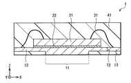
図1は本開示の一実施の形態に係る半導体装置(半導体装置1)の上面構成を表したものである。図2は図1のII−II線に沿った断面構成、図3は図1のIII−III線に沿った断面構成、図4は図1のIV−IV線に沿った断面構成をそれぞれ表している。半導体装置1はQFNパッケージされたものであり、リードフレーム10の表面に設けられた半導体チップ21が封止樹脂41で覆われている。Embodiment
FIG. 1 illustrates a top configuration of a semiconductor device (semiconductor device 1) according to an embodiment of the present disclosure. 2 shows a cross-sectional configuration along line II-II in FIG. 1, FIG. 3 shows a cross-sectional configuration along line III-III in FIG. 1, and FIG. 4 shows a cross-sectional configuration along line IV-IV in FIG. ing. The
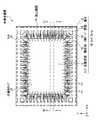
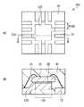
図5(A)はリードフレーム10の表面、図5(B)はその裏面の平面構成をそれぞれ表すものである。図5のドットで表した領域は、図5(A)は表面から、図5(B)は裏面からそれぞれ一定の厚みだけ削られ、他の部分に比べて薄くなっている箇所を表している。5A shows the front surface of the
リードフレーム10は、例えばメッキされた銅(Cu)により構成され、チップ搭載領域11(ダイパッド)、端子12(信号端子)、リード領域13Aおよび端子12とリード領域13Aとの間の間隙14を有している。間隙14と端子12との間には端子12を支持する張出部15(図2)が設けられている。図5(A)のドット領域は張出部15、図5(B)のドット領域はリード領域13Aである。The
チップ搭載領域11はリードフレーム10の中央部に矩形状に設けられ、チップ搭載領域11の周囲にリード領域13Aが設けられている。チップ搭載領域11およびリード領域13Aは連結され、一体化している。このチップ搭載領域11に半導体チップ21が搭載されている。リード領域13Aはその周縁にチップ搭載領域11と同一面内方向の複数の凹凸部を有しており、これら複数の凸部の各々がGNDリード13である。ここでは、リード領域13A(GNDリード13)がチップ搭載領域11を囲む四辺全てに設けられている。 The
端子12は間隙14を間にしてリード領域13Aの凹部にそれぞれ設けられ、リード領域13Aおよびチップ搭載領域11とは電気的に分離されている。換言すれば、端子12はGNDリード13(リード領域13Aの凸部)間に配置されている。また、端子12とチップ搭載領域11との間にはリード領域13Aが存在しているため、端子12はその三方向がリード領域13Aに囲まれている。この端子12は裏面において封止樹脂41から露出され(図2)、ワイヤ31(第1配線)を介して半導体チップ21の電極パッドと電気的に接続されている。一方、半導体チップ21の別の電極パッドはワイヤ31(第2配線)によりGNDリード13に電気的に接続され、GND接続されている。換言すれば、端子12と半導体チップ21を電気的接続するワイヤ31は信号線、GNDリード13と半導体チップ21を電気的に接続するワイヤ31はGND線である。このように、端子12とGNDリード13とを設けることにより、端子12を介して伝達される信号が高周波である場合にも、高周波信号が互いに分離(アイソレーション)され、信号間の干渉を抑えて半導体装置1の高周波特性を向上させることができる。また、全ての端子12間にはGNDリード13が存在するので、ワイヤ31をいずれのGNDリード13に接続することも可能となり、配線の自由度を高めることができる。 The
端子12は、図4に表したように、その配列方向(GNDリード13との並び方向)の断面形状の側壁(側面)が湾曲線の台形状となっている。なお、側壁は直線状であってもよい。端子12の断面形状を台形状にすることで、端子12の裏面の大きさが確保され、半導体装置1の電気的特性を安定化することができる。 As shown in FIG. 4, the terminal 12 has a trapezoidal shape in which the side wall (side surface) of the cross-sectional shape in the arrangement direction (alignment direction with the GND lead 13) is a curved line. The side wall may be linear. By making the cross-sectional shape of the terminal 12 trapezoidal, the size of the back surface of the terminal 12 is ensured, and the electrical characteristics of the
本実施の形態のリードフレーム10では、リード領域13Aの表面からの厚みT2が端子12の表面からの厚みT1に比べて小さい(図2〜図4)。例えば、T1が0.125mmのとき、T2は0.04〜0.09mm程度である。このように、リード領域13Aの厚みT2を端子12の厚みT1よりも小さくすることにより、リード領域13Aの裏面は封止樹脂41に覆われる(図3)。即ち、各々のGNDリード13は外部端子としての機能を有するものではないため、端子12間のピッチP1(図5)を小さくすることができる。よって、半導体チップ21の周囲の外部端子の数を少なくして、半導体装置1を小型化することができる。ピッチP1は、例えば0.4mmであり、端子12とGNDリード13との間のピッチP2は、例えば0.2mmである。 In the
このようなリード領域13Aを含むリードフレーム10は、例えば図6に表したように、ハンダ42を間にして実装基板43に実装され、GND接続される。即ち、一体化したチップ搭載領域11およびリード領域13A全体がGND端子となる。実装基板43への実装時に半導体装置1では、封止樹脂41内での端子12とGNDリード13との間のピッチP2に比べて、封止樹脂41から露出した端子12間のピッチP1が大きくなるため(図5(A))、実装基板43への接続を容易に行うことができる。 For example, as shown in FIG. 6, the
また、本実施の形態のリードフレーム10はリード領域13Aがチップ搭載領域11と一体化していることにより、その強度が向上し、反りや変形の発生を防止することができる。このような反りや変形の発生が抑制されたリードフレーム10では、その搬送が容易となるため、薄い銅箔でリードフレーム10を作製して歩留りを向上させることができる。また、チップ搭載領域11に、リード領域13Aが一体化されていることで、放熱面積が大きくなり、半導体装置1の放熱性も向上する。更に、リード領域13Aが連結しているため、チップ搭載領域11よりも大きなサイズの半導体チップ21の搭載を容易に行うことができる。リードフレーム10に張出部15を設けることにより、チップ搭載領域11よりも大きな半導体チップ21を搭載した場合にも、半導体チップ21と端子12との接触を防ぐと共に端子12の大きさを維持しつつ、小型化することが可能となる。 In addition, since the
半導体チップ21は接着剤22によりチップ搭載領域11に固定され、その電極パッドはワイヤ31により端子12、GNDリード13にそれぞれワイヤボンディングされている。半導体チップ21は、例えば、NPN縦型トランジスタ(NPN Trs)、PNP縦型トランジスタ(V−PNP Trs)、Pチャネル型MOSトランジスタ(PMOS)、Nチャネル型MOSトランジスタ(NMOS)、MOS容量および抵抗(ポリシリコン抵抗)等の複数の半導体素子により構成されている。ワイヤ31は、導電性の金属、例えば金(Au)線からなる。 The
封止樹脂41は半導体チップ21をリードフレーム10に封止するものであり、半導体チップ21およびワイヤ31、更に、リードフレーム10の表面およびリード領域13Aの裏面を覆っている。封止樹脂41は、例えばエポキシ樹脂等の絶縁性樹脂により構成されている。 The sealing
この半導体装置1は、例えば次のようにして製造することができる。 The
まず、図7に表したように、チップ搭載領域11、端子12、リード領域13A、間隙14および張出部15を有するリードフレーム10の裏面にテープ53を貼り合わせる。このリードフレーム10はリードフレームシートに支持部16により支持されている。テープ53は、後の工程で封止樹脂41を形成する際に、リードフレーム10の裏面に樹脂バリが生成するのを防ぐためのものであり、例えば、ポリイミドテープ等からなる。リードフレーム10へのチップ搭載領域11、端子12、リード領域13A、間隙14および張出部15の形成は、金属板を例えば打ち抜きプレス加工やエッチング加工等の適当な加工方法により所定形状にパターニングして行う。 First, as shown in FIG. 7, the
リードフレーム10にテープ53を貼り合わせた後、チップ搭載領域11に半導体チップ21を接着剤22により着設する(図8)。 After bonding the
次いで、半導体チップ21の電極パッドと端子12、GNDリード13とをそれぞれワイヤ31により電気的に接続する(図9)。 Next, the electrode pads of the
続いて、封止樹脂41によりリードフレーム10の表面およびリード領域13Aの裏面、半導体チップ21、ワイヤ31を完全に被覆した後(図10)、リードフレーム10からテープ53を剥離する(図11)。 Subsequently, after completely covering the front surface of the
続いて、封止樹脂41の表面に製品名等のマーク54を刻印した後(図12)、図13に表したようにカッター等により切断線55でリードフレームシートからリードフレーム10を切り離す。以上の工程により、図1〜4に示した半導体装置1が完成する。Subsequently, after a
本実施の形態の半導体装置1では、リード領域13Aの厚みT2が端子12の厚みT1よりも小さいので、半導体チップ21をGND接続してもパッケージサイズが小型化される。
以下、比較例1,2を用いてこれについて詳細に説明する。In the
Hereinafter, this will be described in detail using Comparative Examples 1 and 2.
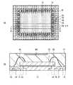
図14は、比較例1に係る半導体装置100の断面構成を表したものである。この半導体装置100では、半導体チップ21の電極パッドをチップ搭載領域111(ダイパッド)にワイヤ31により電気的に接続してGND接続している。このような場合には、チップ搭載領域111に接続領域111A(ボンドエリア)が必要となるため、半導体装置100のパッケージサイズが大きくなる。また、チップ搭載領域111を半導体チップ21よりも小さくすることはできない。 FIG. 14 illustrates a cross-sectional configuration of the
図15は、比較例2に係る半導体装置101の断面構成を表したものであり、図15(A)は平面構成、図15(B)は図15(A)のB−B線に沿った断面構成を表している。この半導体装置101では、チップ搭載領域121に一体化したGNDリード123により半導体チップ21のGND接続がなされている。しかしながら、GNDリード123の裏面は封止樹脂41から露出しているため、GNDリード123は外部端子として機能し、半導体チップ21の周囲の外部端子の数が増加する。即ち、GNDリード123と端子12との間のピッチP100を小さくすることができず、半導体装置101のパッケージサイズは大きくなる。 15 illustrates a cross-sectional configuration of the
これに対し、半導体装置1では、リード領域13Aの厚みT2が端子12の厚みT1よりも小さいので、リード領域13A(GNDリード13)の裏面は封止樹脂41で覆われる。これにより、一体化したチップ搭載領域11およびリード領域13AがGND端子として機能するため、半導体チップ21の周囲の外部端子の数を増加させることなく、半導体チップ21をGND接続することができる。また、チップ搭載領域11に接続領域を設ける必要もない。よって、半導体装置1を小型化することができる。 On the other hand, in the
また、リード領域13Aの凹部に端子12が配置され、端子12がGNDリード13に囲まれているので、半導体装置1の高周波特性が向上する。 Further, since the terminal 12 is disposed in the recess of the
更に、チップ搭載領域11およびリード領域13Aが一体化されているので、リードフレーム10の強度および放熱性が増す。加えて、チップ搭載領域11よりも大きなサイズの半導体チップ21を搭載することも容易に行うことができる。 Furthermore, since the
以上、本実施の形態では、リード領域13Aの厚みT2を端子12の厚みT1よりも小さくするようにしたので、半導体チップ21の周囲の外部端子の数を増やすことなく、また、チップ搭載領域11に接続領域を設けることなく半導体チップ21をGND接続することができる。よって、半導体チップ21をGND接続し、かつ半導体装置1を小型化することができる。 As described above, in the present embodiment, the thickness T2 of the
以下、本技術の変形例について説明するが、上記実施の形態と共通の構成要素については同一符号を付してその説明は省略する。 Hereinafter, although the modified example of this technique is demonstrated, the same code | symbol is attached | subjected about the same component as the said embodiment, and the description is abbreviate | omitted.
〔変形例1〕
図16は、変形例1に係る半導体装置(半導体装置2)の断面構成を表したものである。この半導体装置2は、一のチップ搭載領域11に半導体チップ(半導体チップ21A,21B,21C)を複数有している点で、上記実施の形態の半導体装置1と異なる。この点を除き、この半導体装置2は上記実施の形態の半導体装置1と同様の構成を有し、その作用および効果も同様である。[Modification 1]
FIG. 16 illustrates a cross-sectional configuration of the semiconductor device (semiconductor device 2) according to the first modification. This semiconductor device 2 is different from the
半導体チップ21A,21B,21Cは互いの電極パッド同士がワイヤ31により電気的に接続され、リードフレーム10(チップ搭載領域11)に搭載されている。即ち、この半導体装置2は所謂マルチチップの構成を有するものである。The semiconductor chips 21A, 21B, and 21C are mounted on the lead frame 10 (chip mounting region 11) with their electrode pads electrically connected by
〔変形例2〕
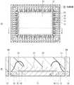
変形例2に係る半導体装置(半導体装置3)は、チップ搭載領域(チップ搭載領域11A,11B,11C)が複数設けられたリードフレーム50を有するものである。この点を除き、この半導体装置3は上記実施の形態の半導体装置1と同様の構成を有し、その作用および効果も同様である。[Modification 2]
The semiconductor device (semiconductor device 3) according to Modification 2 has a
図17,図18に表したように、リードフレーム50は間隙により分離された3つのチップ搭載領域11A,11B,11Cを有するものであるが、チップ搭載領域11A,11B,11C各々に一体化したリード領域13Aは共通であり連結している。例えば、複数の半導体チップ21A,21B,21Cを半導体装置3に搭載させる場合(図18)に、電源電位ごとにチップ搭載領域11A,11B,11Cを分けるようにしてもよい。リードフレーム50では複数のGNDリード13が一体化されているので(リード領域13A)、チップ搭載領域11A,11B,11Cを分割しても一のリードフレーム50で半導体チップ21A,21B,21Cを保持することが可能となる。 As shown in FIGS. 17 and 18, the
以上、実施の形態および変形例を挙げて本技術を説明したが、本技術は上記実施の形態等に限定されるものではなく、種々変形可能である。例えば、上記実施の形態では、リード領域13AをGND接続する場合について説明したが、GND以外の電位に接続するようにしてもよい。 As described above, the present technology has been described with reference to the embodiment and the modification. However, the present technology is not limited to the above-described embodiment and the like, and various modifications can be made. For example, in the above embodiment, the case where the
また、上記実施の形態等では、半導体装置1のパッケージがQFN型である場合について説明したが、QFN型以外のパッケージ型、例えばSON等であってもよい。 In the above-described embodiment and the like, the case where the package of the
更に、例えば、上記実施の形態等において説明した各部の材料および厚み、または形成方法および形成条件などは限定されるものではなく、他の材料および厚みとしてもよく、または他の形成方法および形成条件としてもよい。 Furthermore, for example, the material and thickness of each part described in the above embodiments and the like, or the forming method and forming conditions are not limited, and may be other materials and thicknesses, or other forming methods and forming conditions. It is good.
なお、本技術は、以下のような構成も可能である。
(1)表面に設けられたチップ搭載領域と、前記チップ搭載領域と同一面内方向の複数の凹凸部を含むリード領域と、前記凹部に配置された端子とを備え、前記リード領域の表面からの厚みは、前記端子の表面からの厚みよりも小さいリードフレーム。
(2)前記リード領域は前記チップ搭載領域と一体化し、前記リード領域と前記端子とは電気的に分離されている前記(1)記載のリードフレーム。
(3)前記端子の断面形状は台形状である前記(1)または(2)記載のリードフレーム。
(4)中央部に前記チップ搭載領域、前記チップ搭載領域の周囲に前記リード領域が設けられ、
前記リード領域の凹部全てに前記端子が配置されている前記(1)乃至(3)のうちいずれか1つに記載のリードフレーム。
(5)半導体チップおよびリードフレームを備え、前記リードフレームは、表面に設けられたチップ搭載領域と、前記チップ搭載領域と同一面内方向の複数の凹凸部を含むリード領域と、前記凹部に配置された端子とを有すると共に、前記リード領域の表面からの厚みが、前記端子の表面からの厚みよりも小さく、前記半導体チップは、前記チップ搭載領域に搭載されると共に、第1配線により前記端子に、第2配線により前記リード領域にそれぞれ電気的に接続されている半導体装置。
(6)前記半導体チップは前記チップ搭載領域よりも大きい前記(5)記載の半導体装置。
(7)前記半導体チップと共に前記リードフレームの表面と前記リード領域の裏面とが封止樹脂に覆われ、前記端子の裏面は前記封止樹脂から露出されている前記(5)または(6)記載の半導体装置。
(8)前記半導体チップおよび前リードフレームはQFN(Quad Flat Non-leaded Package)パッケージされている前記(5)乃至(7)のうちいずれか1つに記載の半導体装置。
(9)前記リード領域は前記チップ搭載領域と一体化し、前記リード領域と前記端子とは電気的に分離されている前記(5)乃至(8)のうちいずれか1つに記載の半導体装置。
(10)前記第1配線は信号線、前記第2配線はグラウンド(GND)線である前記(5)乃至(9)のうちいずれか1つに記載の半導体装置。
(11)一の前記チップ搭載領域に前記半導体チップを複数有する前記(5)乃至(10)のうちいずれか1つに記載の半導体装置。
(12)前記リードフレームは間隙により分離された複数のチップ搭載領域を有し、前記複数のチップ搭載領域それぞれのリード領域は共通である前記(9)または(10)記載の半導体装置。
Note that the present technology may be configured as follows.
(1) A chip mounting region provided on the surface, a lead region including a plurality of concave and convex portions in the same plane direction as the chip mounting region, and a terminal disposed in the concave portion, and from the surface of the lead region The lead frame is smaller than the thickness from the surface of the terminal.
(2) The lead frame according to (1), wherein the lead region is integrated with the chip mounting region, and the lead region and the terminal are electrically separated.
(3) The lead frame according to (1) or (2), wherein the terminal has a trapezoidal cross-sectional shape.
(4) The chip mounting area at the center, and the lead area around the chip mounting area,
The lead frame according to any one of (1) to (3), wherein the terminals are arranged in all the concave portions of the lead region.
(5) A semiconductor chip and a lead frame are provided, and the lead frame is arranged in the chip mounting region provided on the surface, a lead region including a plurality of concave and convex portions in the same plane direction as the chip mounting region, and the recess. And the thickness from the surface of the lead region is smaller than the thickness from the surface of the terminal, and the semiconductor chip is mounted on the chip mounting region and the terminal is connected by a first wiring. And a semiconductor device electrically connected to the lead region by a second wiring.
(6) The semiconductor device according to (5), wherein the semiconductor chip is larger than the chip mounting area.
(7) The above (5) or (6), wherein the surface of the lead frame and the back surface of the lead region are covered with a sealing resin together with the semiconductor chip, and the back surface of the terminal is exposed from the sealing resin. Semiconductor device.
(8) The semiconductor device according to any one of (5) to (7), wherein the semiconductor chip and the front lead frame are packaged in a QFN (Quad Flat Non-leaded Package) package.
(9) The semiconductor device according to any one of (5) to (8), wherein the lead region is integrated with the chip mounting region, and the lead region and the terminal are electrically separated.
(10) The semiconductor device according to any one of (5) to (9), wherein the first wiring is a signal line, and the second wiring is a ground (GND) line.
(11) The semiconductor device according to any one of (5) to (10), wherein a plurality of the semiconductor chips are provided in one chip mounting region.
(12) The semiconductor device according to (9) or (10), wherein the lead frame has a plurality of chip mounting areas separated by a gap, and each of the plurality of chip mounting areas has a common lead area.
1・・・半導体装置、10,10A,10B,50・・・リードフレーム、11,11A,11B,11C・・・チップ搭載領域、12・・・端子、13・・・GNDリード、13A・・・リード領域、14・・・間隙、15・・・張出部、21,21A,21B,21C・・・半導体チップ、31・・・ワイヤ、41・・・封止樹脂。DESCRIPTION OF
Claims (11)
Translated fromJapanese前記チップ搭載領域と一体化して設けられ、かつ前記チップ搭載領域と同一の平面を成して前記半導体チップから突出する複数の凸部を含むリード領域と、
前記凸部同士の間の領域に、前記リード領域とは電気的に分離して配置された端子とを備え、
前記リード領域の表面からの厚みは、前記端子の表面からの厚みよりも小さく、
前記半導体チップは、前記チップ搭載領域よりも大きく、かつ第1配線により前記端子に、第2配線により前記リード領域の凸部にそれぞれ電気的に接続される
リードフレーム。A chip mounting areawhere a semiconductor chip is mounted on the surface;
A lead region that includes the provided integrally with the chip mounting region, and a plurality of protrusionsprojecting from said by forming the same plane as the chip mounting regionsemiconductor chip,
In a region between the convex portions, the lead region is provided with a terminal that is electrically separated from the lead region,
The thickness from the surface of the lead region israther smaller than the thickness from the surface of theterminal,
The semiconductor chip is larger than the chip mounting area, and is electrically connected to the terminal by a first wiring and to a convex portion of the lead area by a second wiring .
請求項1に記載のリードフレーム。The lead frame of claim 1 including a gap in the sealing resin between thefront SL terminal and the lead region.
請求項1記載のリードフレーム。The lead frame according to claim 1, wherein the terminal has a trapezoidal cross-sectional shape.
隣り合う前記凸部の間の全てに前記端子が配置されている
請求項1記載のリードフレーム。The chip mounting area in the center, the lead area is provided around the chip mounting area,
The lead frame according to claim 1, wherein the terminals are disposedbetween allthe adjacent convex portions .
前記リードフレームは、
表面に前記半導体チップが搭載されるチップ搭載領域と、
前記チップ搭載領域と一体化して設けられ、かつ前記チップ搭載領域と同一の平面を成して前記半導体チップから突出する複数の凸部を含むリード領域と、
前記凸部同士の間の領域に、前記リード領域とは電気的に分離して配置された端子とを有すると共に、前記リード領域の表面からの厚みが、前記端子の表面からの厚みよりも小さく、
前記半導体チップは、前記チップ搭載領域よりも大きく、かつ第1配線により前記端子に、第2配線により前記リード領域の凸部にそれぞれ電気的に接続されている
半導体装置。With semiconductor chip and lead frame,
The lead frame is
A chip mounting areawhere the semiconductor chip is mounted on the surface;
A lead region that includes the provided integrally with the chip mounting region, and a plurality of protrusionsprojecting from said by forming the same plane as the chip mounting regionsemiconductor chip,
The area between the protrusions has a terminal that is electrically separated from the lead area, and the thickness from the surface of the lead area is smaller than the thickness from the surface of the terminal. ,
The semiconductor device islarger than the chip mounting region, and is electrically connected to the terminal by a first wiring and toa convex portion of the lead region by a second wiring.
前記端子の裏面は前記封止樹脂から露出されている
請求項5記載の半導体装置。The surface of the lead frame and the back surface of the lead region together with the semiconductor chip are covered with a sealing resin,
The semiconductor device according to claim 5, wherein a back surface of the terminal is exposed from the sealing resin.
請求項6記載の半導体装置。The semiconductor device according to claim6, wherein the semiconductor chip and the lead frame are packaged in a QFN (Quad Flat Non-leaded Package) package.
請求項6に記載の半導体装置。The semiconductor device of claim6 including the sealing resin into the gap between thepre-Symbol terminal and the lead region.
請求項5記載の半導体装置。The semiconductor device according to claim 5, wherein the first wiring is a signal line, and the second wiring is a ground (GND) line.
請求項5記載の半導体装置。The semiconductor device according to claim 5, wherein a plurality of the semiconductor chips are provided in one chip mounting region.
前記複数のチップ搭載領域を囲って前記リード領域が設けられている
請求項8記載の半導体装置。The lead frame has a plurality of chip mounting areas separated by gaps,
The semiconductor device according to claim8, wherein the lead region is provided so as to surround the plurality of chip mounting regions.
Priority Applications (3)
| Application Number | Priority Date | Filing Date | Title |
|---|---|---|---|
| JP2011239444AJP5953703B2 (en) | 2011-10-31 | 2011-10-31 | Lead frame and semiconductor device |
| US13/659,557US8928136B2 (en) | 2011-10-31 | 2012-10-24 | Lead frame semiconductor device |
| CN201210423881.9ACN103094238B (en) | 2011-10-31 | 2012-10-24 | Lead frame and semiconductor devices |
Applications Claiming Priority (1)
| Application Number | Priority Date | Filing Date | Title |
|---|---|---|---|
| JP2011239444AJP5953703B2 (en) | 2011-10-31 | 2011-10-31 | Lead frame and semiconductor device |
Publications (3)
| Publication Number | Publication Date |
|---|---|
| JP2013098332A JP2013098332A (en) | 2013-05-20 |
| JP2013098332A5 JP2013098332A5 (en) | 2014-11-27 |
| JP5953703B2true JP5953703B2 (en) | 2016-07-20 |
Family
ID=48171542
Family Applications (1)
| Application Number | Title | Priority Date | Filing Date |
|---|---|---|---|
| JP2011239444AExpired - Fee RelatedJP5953703B2 (en) | 2011-10-31 | 2011-10-31 | Lead frame and semiconductor device |
Country Status (3)
| Country | Link |
|---|---|
| US (1) | US8928136B2 (en) |
| JP (1) | JP5953703B2 (en) |
| CN (1) | CN103094238B (en) |
Families Citing this family (13)
| Publication number | Priority date | Publication date | Assignee | Title |
|---|---|---|---|---|
| JP6352009B2 (en)* | 2013-04-16 | 2018-07-04 | ローム株式会社 | Semiconductor device |
| CN103337488B (en)* | 2013-06-05 | 2016-09-14 | 吉林华微斯帕克电气有限公司 | A kind of lead frame |
| JP6413709B2 (en)* | 2014-12-02 | 2018-10-31 | 富士電機株式会社 | Semiconductor device and manufacturing method thereof |
| US9966326B2 (en)* | 2015-03-16 | 2018-05-08 | Unisem (M) Berhad | Lead frames with wettable flanks |
| JP6507779B2 (en)* | 2015-03-26 | 2019-05-08 | セイコーエプソン株式会社 | Electro-optical device, method of manufacturing electro-optical device, and electronic apparatus |
| JP6555927B2 (en)* | 2015-05-18 | 2019-08-07 | 大口マテリアル株式会社 | Semiconductor device mounting lead frame and semiconductor device manufacturing method |
| JP6923299B2 (en) | 2016-09-26 | 2021-08-18 | 株式会社アムコー・テクノロジー・ジャパン | Semiconductor devices and methods for manufacturing semiconductor devices |
| JP6772087B2 (en)* | 2017-02-17 | 2020-10-21 | 新光電気工業株式会社 | Lead frame and its manufacturing method |
| US10679929B2 (en)* | 2017-07-28 | 2020-06-09 | Advanced Semiconductor Engineering Korea, Inc. | Semiconductor package device and method of manufacturing the same |
| US20190221502A1 (en)* | 2018-01-17 | 2019-07-18 | Microchip Technology Incorporated | Down Bond in Semiconductor Devices |
| CN110828442A (en)* | 2019-11-04 | 2020-02-21 | 弘凯光电(深圳)有限公司 | Packaging structure and manufacturing method thereof |
| CN115706071A (en)* | 2021-08-13 | 2023-02-17 | 江苏长电科技股份有限公司 | QFN (quad Flat No lead) packaging structure and manufacturing method thereof |
| CN115706068A (en)* | 2021-08-13 | 2023-02-17 | 江苏长电科技股份有限公司 | QFN (quad Flat No lead) packaging structure and manufacturing method thereof |
Family Cites Families (28)
| Publication number | Priority date | Publication date | Assignee | Title |
|---|---|---|---|---|
| US5084753A (en)* | 1989-01-23 | 1992-01-28 | Analog Devices, Inc. | Packaging for multiple chips on a single leadframe |
| JPH0621319A (en)* | 1992-06-30 | 1994-01-28 | Nec Corp | Lead frame for semiconductor device |
| JP2811170B2 (en)* | 1996-06-28 | 1998-10-15 | 株式会社後藤製作所 | Resin-sealed semiconductor device and method of manufacturing the same |
| DE19808193B4 (en)* | 1998-02-27 | 2007-11-08 | Robert Bosch Gmbh | Leadframe device and corresponding manufacturing method |
| JPH11340405A (en)* | 1998-05-22 | 1999-12-10 | Fujitsu Quantum Devices Kk | Lead frame, semiconductor device and manufacture thereof |
| KR100526844B1 (en)* | 1999-10-15 | 2005-11-08 | 앰코 테크놀로지 코리아 주식회사 | semiconductor package and its manufacturing method |
| US6198171B1 (en)* | 1999-12-30 | 2001-03-06 | Siliconware Precision Industries Co., Ltd. | Thermally enhanced quad flat non-lead package of semiconductor |
| TW447059B (en)* | 2000-04-28 | 2001-07-21 | Siliconware Precision Industries Co Ltd | Multi-chip module integrated circuit package |
| JP2001313363A (en)* | 2000-05-01 | 2001-11-09 | Rohm Co Ltd | Resin-encapsulated semiconductor device |
| JP2002026190A (en)* | 2000-07-03 | 2002-01-25 | Dainippon Printing Co Ltd | Resin-sealed semiconductor device |
| US6661082B1 (en)* | 2000-07-19 | 2003-12-09 | Fairchild Semiconductor Corporation | Flip chip substrate design |
| JP3895570B2 (en)* | 2000-12-28 | 2007-03-22 | 株式会社ルネサステクノロジ | Semiconductor device |
| US6720207B2 (en)* | 2001-02-14 | 2004-04-13 | Matsushita Electric Industrial Co., Ltd. | Leadframe, resin-molded semiconductor device including the leadframe, method of making the leadframe and method for manufacturing the device |
| JP2003204027A (en)* | 2002-01-09 | 2003-07-18 | Matsushita Electric Ind Co Ltd | Lead frame and method of manufacturing the same, resin-sealed semiconductor device and method of manufacturing the same |
| AU2003235967A1 (en) | 2002-04-30 | 2003-11-17 | Renesas Technology Corp. | Semiconductor device and electronic device |
| JP4149439B2 (en)* | 2002-07-01 | 2008-09-10 | 株式会社ルネサステクノロジ | Semiconductor device |
| JP2004071801A (en)* | 2002-08-06 | 2004-03-04 | Shinko Electric Ind Co Ltd | Lead frame and its fabricating method |
| US20040124508A1 (en)* | 2002-11-27 | 2004-07-01 | United Test And Assembly Test Center Ltd. | High performance chip scale leadframe package and method of manufacturing the package |
| JP2005057067A (en)* | 2003-08-05 | 2005-03-03 | Renesas Technology Corp | Semiconductor device and manufacturing method thereof |
| JP2005191342A (en)* | 2003-12-26 | 2005-07-14 | Renesas Technology Corp | Semiconductor device and manufacturing method thereof |
| US7247937B2 (en)* | 2005-01-06 | 2007-07-24 | Via Technologies, Inc. | Mounting pad structure for wire-bonding type lead frame packages |
| JP2007012857A (en)* | 2005-06-30 | 2007-01-18 | Renesas Technology Corp | Semiconductor device |
| US7301225B2 (en)* | 2006-02-28 | 2007-11-27 | Freescale Semiconductor, Inc. | Multi-row lead frame |
| JP4652281B2 (en) | 2006-05-29 | 2011-03-16 | パナソニック株式会社 | Resin-sealed semiconductor device |
| US7556987B2 (en)* | 2006-06-30 | 2009-07-07 | Stats Chippac Ltd. | Method of fabricating an integrated circuit with etched ring and die paddle |
| CN101601133B (en)* | 2006-10-27 | 2011-08-10 | 宇芯(毛里求斯)控股有限公司 | Partially patterned leadframe and methods of making and using same in semiconductor package |
| CN101308832B (en)* | 2007-05-17 | 2010-06-16 | 南茂科技股份有限公司 | Lead frame for leadless package, package structure thereof and manufacturing method thereof |
| JP5184558B2 (en)* | 2010-01-18 | 2013-04-17 | ルネサスエレクトロニクス株式会社 | Semiconductor device |
- 2011
- 2011-10-31JPJP2011239444Apatent/JP5953703B2/ennot_activeExpired - Fee Related
- 2012
- 2012-10-24USUS13/659,557patent/US8928136B2/ennot_activeExpired - Fee Related
- 2012-10-24CNCN201210423881.9Apatent/CN103094238B/ennot_activeExpired - Fee Related
Also Published As
| Publication number | Publication date |
|---|---|
| JP2013098332A (en) | 2013-05-20 |
| US8928136B2 (en) | 2015-01-06 |
| CN103094238A (en) | 2013-05-08 |
| US20130105957A1 (en) | 2013-05-02 |
| CN103094238B (en) | 2017-07-14 |
Similar Documents
| Publication | Publication Date | Title |
|---|---|---|
| JP5953703B2 (en) | Lead frame and semiconductor device | |
| US6627977B1 (en) | Semiconductor package including isolated ring structure | |
| TW575955B (en) | Leadframe and method of manufacturing a semiconductor device using the same | |
| US7808084B1 (en) | Semiconductor package with half-etched locking features | |
| US9275945B2 (en) | Method of manufacturing semiconductor device and semiconductor device | |
| JP5802695B2 (en) | Semiconductor device and method for manufacturing semiconductor device | |
| WO2004004005A1 (en) | Semiconductor device and its manufacturing method | |
| US20050051877A1 (en) | Semiconductor package having high quantity of I/O connections and method for fabricating the same | |
| US7531895B2 (en) | Integrated circuit package and method of manufacture thereof | |
| KR20040026130A (en) | Lead frame and method of manufacturing the same | |
| US6163069A (en) | Semiconductor device having pads for connecting a semiconducting element to a mother board | |
| JP2005026466A (en) | Semiconductor device and lead frame | |
| JP3470111B2 (en) | Method for manufacturing resin-encapsulated semiconductor device | |
| JP2005085089A (en) | Ic card and manufacturing method thereof | |
| US20080073763A1 (en) | Semiconductor device and method of manufacturing the same | |
| JP2016201447A (en) | Mold package | |
| JP3877732B2 (en) | Lead frame, semiconductor device using the same, and method for manufacturing the semiconductor device | |
| CN113937074A (en) | Quad flat non-leaded package structure | |
| JP4305326B2 (en) | Manufacturing method of semiconductor package | |
| JP6494723B2 (en) | Semiconductor package | |
| JP2533011B2 (en) | Surface mount semiconductor device | |
| JP4409528B2 (en) | Semiconductor device | |
| US20250218907A1 (en) | Leadframe with retaining features | |
| JP2007134585A (en) | Semiconductor device and its manufacturing method | |
| US11810840B2 (en) | Semiconductor device |
Legal Events
| Date | Code | Title | Description |
|---|---|---|---|
| A521 | Request for written amendment filed | Free format text:JAPANESE INTERMEDIATE CODE: A523 Effective date:20141015 | |
| A621 | Written request for application examination | Free format text:JAPANESE INTERMEDIATE CODE: A621 Effective date:20141015 | |
| A977 | Report on retrieval | Free format text:JAPANESE INTERMEDIATE CODE: A971007 Effective date:20150817 | |
| A131 | Notification of reasons for refusal | Free format text:JAPANESE INTERMEDIATE CODE: A131 Effective date:20150908 | |
| A521 | Request for written amendment filed | Free format text:JAPANESE INTERMEDIATE CODE: A523 Effective date:20151007 | |
| A131 | Notification of reasons for refusal | Free format text:JAPANESE INTERMEDIATE CODE: A131 Effective date:20160301 | |
| A521 | Request for written amendment filed | Free format text:JAPANESE INTERMEDIATE CODE: A523 Effective date:20160419 | |
| TRDD | Decision of grant or rejection written | ||
| A01 | Written decision to grant a patent or to grant a registration (utility model) | Free format text:JAPANESE INTERMEDIATE CODE: A01 Effective date:20160517 | |
| A61 | First payment of annual fees (during grant procedure) | Free format text:JAPANESE INTERMEDIATE CODE: A61 Effective date:20160530 | |
| R151 | Written notification of patent or utility model registration | Ref document number:5953703 Country of ref document:JP Free format text:JAPANESE INTERMEDIATE CODE: R151 | |
| R250 | Receipt of annual fees | Free format text:JAPANESE INTERMEDIATE CODE: R250 | |
| R250 | Receipt of annual fees | Free format text:JAPANESE INTERMEDIATE CODE: R250 | |
| LAPS | Cancellation because of no payment of annual fees |