Movatterモバイル変換


[0]ホーム

URL:


JP5948666B2 - Illumination light source and illumination device - Google Patents

Illumination light source and illumination device
Download PDF

Info

Publication number
JP5948666B2
JP5948666B2JP2012256695AJP2012256695AJP5948666B2JP 5948666 B2JP5948666 B2JP 5948666B2JP 2012256695 AJP2012256695 AJP 2012256695AJP 2012256695 AJP2012256695 AJP 2012256695AJP 5948666 B2JP5948666 B2JP 5948666B2
Authority
JP
Japan
Prior art keywords
housing
casing
led
light
base
Prior art date
Legal status (The legal status is an assumption and is not a legal conclusion. Google has not performed a legal analysis and makes no representation as to the accuracy of the status listed.)
Active
Application number
JP2012256695A
Other languages
Japanese (ja)
Other versions
JP2014107022A (en
Inventor
健太 渡邉
健太 渡邉
和生 合田
和生 合田
直紀 田上
直紀 田上
考志 大村
考志 大村
次弘 松田
次弘 松田
Current Assignee (The listed assignees may be inaccurate. Google has not performed a legal analysis and makes no representation or warranty as to the accuracy of the list.)
Panasonic Intellectual Property Management Co Ltd
Original Assignee
Panasonic Intellectual Property Management Co Ltd
Priority date (The priority date is an assumption and is not a legal conclusion. Google has not performed a legal analysis and makes no representation as to the accuracy of the date listed.)
Filing date
Publication date
Application filed by Panasonic Intellectual Property Management Co LtdfiledCriticalPanasonic Intellectual Property Management Co Ltd
Priority to JP2012256695ApriorityCriticalpatent/JP5948666B2/en
Publication of JP2014107022ApublicationCriticalpatent/JP2014107022A/en
Application grantedgrantedCritical
Publication of JP5948666B2publicationCriticalpatent/JP5948666B2/en
Activelegal-statusCriticalCurrent
Anticipated expirationlegal-statusCritical

Links

Images

Landscapes

Description

Translated fromJapanese

本発明は、照明用光源及び照明装置に関し、特に、発光ダイオード(LED:Light Emitting Diode)を用いた電球形ランプ及びこれを用いた照明装置に関する。  The present invention relates to an illumination light source and an illumination device, and more particularly, to a light bulb shaped lamp using a light emitting diode (LED) and an illumination device using the same.

LED等の半導体発光素子は、小型、高効率及び長寿命であることから、様々な製品の光源として期待されている。中でも、電球形LEDランプ(LED電球)は、従来から知られる電球形蛍光灯や白熱電球に代替する照明用光源として開発が進められている(特許文献1)。  Semiconductor light emitting devices such as LEDs are expected to be light sources for various products because of their small size, high efficiency, and long life. Among these, a bulb-type LED lamp (LED bulb) is being developed as an illumination light source that replaces conventionally known bulb-type fluorescent lamps and incandescent bulbs (Patent Document 1).

電球形LEDランプは、例えば、LEDモジュールと、LEDモジュールを覆うグローブと、LEDモジュールを支持する支持部材と、LEDモジュールに電力を供給する駆動回路と、駆動回路を囲むように構成された外郭筐体と、電力を受電する口金とを備える。  The bulb-type LED lamp includes, for example, an LED module, a globe that covers the LED module, a support member that supports the LED module, a drive circuit that supplies power to the LED module, and an outer casing that is configured to surround the drive circuit. A body and a base for receiving power.

特開2006−313717号公報JP 2006-313717 A

LEDランプでは、LEDから熱が発生し、この熱によって、LEDの発光効率が低下するという問題がある。また、LEDは、従来の光源に比べて光による放熱の割合が小さい。  In the LED lamp, there is a problem that heat is generated from the LED and the light emission efficiency of the LED is lowered by this heat. In addition, the LED has a smaller rate of heat radiation due to light than a conventional light source.

このため、電球形LEDランプでは、放熱性の観点から、高温部の表面積を最大限に広げることが好ましい。そこで、LEDで発生する熱の放熱性を向上させるために、ヒートシンクを用いることが考えられる。この場合、例えば、外郭筐体を金属製にしてヒートシンクとして用いたり、外郭筐体の内部に別途金属製のヒートシンクを設けたりすることが考えられる。これにより、LEDで発生した熱を、ヒートシンクを介してLED電球の表面全体に伝えることができる。  For this reason, in the light bulb shaped LED lamp, it is preferable to maximize the surface area of the high temperature part from the viewpoint of heat dissipation. Therefore, it is conceivable to use a heat sink in order to improve the heat dissipation of the heat generated by the LED. In this case, for example, it is conceivable that the outer casing is made of metal and used as a heat sink, or a metal heat sink is separately provided inside the outer casing. Thereby, the heat generated in the LED can be transmitted to the entire surface of the LED bulb through the heat sink.

一方、絶縁性の観点から、金属製のヒートシンクは、樹脂製の絶縁カバーによって覆われていることが好ましい。この場合、放熱理論上、ヒートシンクと絶縁カバーとは密着させることが好ましい。絶縁カバーは、樹脂の靭性を問わず、外郭筐体として使用することができる。  On the other hand, from the viewpoint of insulation, the metal heat sink is preferably covered with a resin insulating cover. In this case, it is preferable that the heat sink and the insulating cover are in close contact with each other in terms of heat dissipation. The insulating cover can be used as an outer casing regardless of the toughness of the resin.

しかしながら、外郭筐体である樹脂製の絶縁カバーとその内側の金属製のヒートシンクとを接触させた状態で温度が変化すると、樹脂と金属とでは線膨張係数(熱膨張係数)が大きく異なるので、樹脂製の絶縁カバーにクラックが生じるという問題がある。特に、低温環境である場合に、絶縁カバーにクラックが生じやすい。  However, when the temperature changes in a state where the insulating cover made of resin, which is the outer casing, and the metal heat sink inside it are in contact, the linear expansion coefficient (thermal expansion coefficient) differs greatly between the resin and the metal. There is a problem that cracks occur in the insulating cover made of resin. In particular, cracks are likely to occur in the insulating cover in a low temperature environment.

本発明は、このような問題を解決するためになされたものであり、外郭をなす筐体にクラックが発生することを防止できる照明用光源及び照明装置を提供することを目的とする。  The present invention has been made to solve such a problem, and an object of the present invention is to provide an illumination light source and an illumination apparatus that can prevent cracks from occurring in a casing that forms an outer shell.

上記目的を達成するために、本発明に係る照明用光源の一態様は、発光モジュールと、前記発光モジュールを発光させるための駆動回路と、前記駆動回路を囲むように構成された第1筐体と、前記第1筐体を囲むように構成されるとともに外郭をなす第2筐体と、を備え、前記第2筐体の線膨張係数は、前記第1筐体の線膨張係数よりも大きく、前記第1筐体と前記第2筐体との間には隙間が設けられていることを特徴とする。  In order to achieve the above object, one aspect of an illumination light source according to the present invention includes a light emitting module, a driving circuit for causing the light emitting module to emit light, and a first housing configured to surround the driving circuit. And a second casing that is configured to surround the first casing and forms an outer shell, and a linear expansion coefficient of the second casing is larger than a linear expansion coefficient of the first casing A gap is provided between the first casing and the second casing.

また、本発明に係る照明用光源の一態様において、前記第1筐体及び前記第2筐体の各々は、円筒部材であり、前記隙間は、前記第1筐体の外周面と前記第2筐体の内周面との間に設けられている、としてもよい。  In the aspect of the illumination light source according to the present invention, each of the first casing and the second casing is a cylindrical member, and the gap is formed between the outer peripheral surface of the first casing and the second casing. It may be provided between the inner peripheral surface of the housing.

また、本発明に係る照明用光源の一態様において、前記第1筐体及び前記第2筐体の各々は、前記円筒部材の内方に向かって折れ曲がるように設けられた屈曲部を有し、前記第1筐体の前記屈曲部の外面と前記第2筐体の前記屈曲部の内面とが接触している、としてもよい。  Further, in one aspect of the illumination light source according to the present invention, each of the first housing and the second housing has a bent portion provided to bend inward of the cylindrical member, The outer surface of the bent portion of the first housing may be in contact with the inner surface of the bent portion of the second housing.

また、本発明に係る照明用光源の一態様において、前記第1筐体は、金属製であり、前記第2筐体は、樹脂製である、としてもよい。  In the aspect of the illumination light source according to the present invention, the first housing may be made of metal, and the second housing may be made of resin.

また、本発明に係る照明用光源の一態様において、さらに、前記第1筐体の内側に配置されるとともに前記駆動回路を囲むように構成された回路ケースを備え、前記第1筐体と前記回路ケースとの間には隙間が設けられている、としてもよい。  In one aspect of the illumination light source according to the present invention, the light source for illumination further includes a circuit case disposed inside the first housing and configured to surround the drive circuit, the first housing and the A gap may be provided between the circuit case and the circuit case.

また、本発明に係る照明用光源の一態様において、前記第1筐体と前記第2筐体との間の隙間は、前記第1筐体と前記回路ケースとの間の隙間よりも小さい、としてもよい。  Further, in one aspect of the illumination light source according to the present invention, a gap between the first casing and the second casing is smaller than a gap between the first casing and the circuit case. It is good.

また、本発明に係る照明用光源の一態様において、さらに、前記発光モジュールを支持する支持部材を備え、前記第1筐体は、前記支持部材と接触している、としてもよい。  Moreover, the aspect of the light source for illumination according to the present invention may further include a support member that supports the light emitting module, and the first housing is in contact with the support member.

また、本発明に係る照明装置の一態様は、上記いずれかに記載の照明用光源を備えることを特徴とする。  In addition, an aspect of the illumination device according to the present invention includes any one of the illumination light sources described above.

本発明によれば、第1筐体を囲む第2筐体の線膨張係数が第1筐体の線膨張係数よりも大きいような場合であっても、外郭をなす第2筐体にクラックが発生することを抑制することができる。  According to the present invention, even if the linear expansion coefficient of the second casing surrounding the first casing is larger than the linear expansion coefficient of the first casing, the second casing forming the outer shell is cracked. Generation | occurrence | production can be suppressed.

図1は、本発明の実施の形態に係る電球形ランプの外観斜視図である。FIG. 1 is an external perspective view of a light bulb shaped lamp according to an embodiment of the present invention.図2は、本発明の実施の形態に係る電球形ランプの分解斜視図である。FIG. 2 is an exploded perspective view of the light bulb shaped lamp according to the embodiment of the present invention.図3は、本発明の実施の形態に係る電球形ランプの断面図である。FIG. 3 is a cross-sectional view of the light bulb shaped lamp according to the embodiment of the present invention.図4(a)は、本発明の実施の形態に係る電球形ランプにおけるLEDモジュールの平面図であり、図4(b)は、(a)のX−X’線における同LEDモジュールの断面図である。図4(c)は、(c)のY−Y’線における同LEDモジュールの断面図である。Fig.4 (a) is a top view of the LED module in the lightbulb-shaped lamp which concerns on embodiment of this invention, FIG.4 (b) is sectional drawing of the LED module in the XX 'line | wire of (a). It is. FIG.4 (c) is sectional drawing of the LED module in the Y-Y 'line | wire of (c).図5は、本発明の実施の形態に係る電球形ランプのLEDモジュールにおけるLED(LEDチップ)周辺の拡大断面図である。FIG. 5 is an enlarged cross-sectional view around the LED (LED chip) in the LED module of the light bulb shaped lamp according to the embodiment of the present invention.図6は、本発明の実施の形態に係る電球形ランプの要部拡大断面図である。FIG. 6 is an enlarged cross-sectional view of a main part of the light bulb shaped lamp according to the embodiment of the present invention.図7は、本発明の実施の形態の変形例1に係る電球形ランプの要部拡大断面図である。FIG. 7 is an enlarged cross-sectional view of a main part of a light bulb shaped lamp according to a first modification of the embodiment of the present invention.図8は、本発明の実施の形態の変形例2に係る電球形ランプの要部拡大断面図である。FIG. 8 is an enlarged cross-sectional view of a main part of a light bulb shaped lamp according to a second modification of the embodiment of the present invention.図9は、本発明の実施の形態に係る照明装置の概略断面図である。FIG. 9 is a schematic cross-sectional view of the illumination device according to the embodiment of the present invention.

以下、本発明の実施の形態に係る照明用光源及び照明装置について、図面を参照しながら説明する。なお、以下に説明する実施の形態は、いずれも本発明の好ましい一具体例を示すものである。したがって、以下の実施の形態で示される、数値、形状、材料、構成要素、構成要素の配置位置及び接続形態などは、一例であって本発明を限定する主旨ではない。よって、以下の実施の形態における構成要素のうち、本発明の最上位概念を示す独立請求項に記載されていない構成要素については、任意の構成要素として説明される。  DESCRIPTION OF EMBODIMENTS Hereinafter, an illumination light source and an illumination device according to embodiments of the present invention will be described with reference to the drawings. Each of the embodiments described below shows a preferred specific example of the present invention. Therefore, the numerical values, shapes, materials, components, component arrangement positions, connection forms, and the like shown in the following embodiments are merely examples, and are not intended to limit the present invention. Therefore, among the constituent elements in the following embodiments, constituent elements that are not described in the independent claims showing the highest concept of the present invention are described as optional constituent elements.

なお、各図は、模式図であり、必ずしも厳密に図示されたものではない。また、各図において、同じ構成部材については同じ符号を付している。  Each figure is a schematic diagram and is not necessarily illustrated strictly. Moreover, in each figure, the same code | symbol is attached | subjected about the same structural member.

以下の実施の形態では、照明用光源の一例として、電球形LEDランプ(LED電球)について説明する。  In the following embodiments, a bulb-type LED lamp (LED bulb) will be described as an example of a light source for illumination.

(電球形ランプの全体構成)
まず、本実施の形態に係る電球形ランプ1の全体構成について、図1及び図2を用いて説明する。図1は、本発明の実施の形態に係る電球形ランプの外観斜視図である。また、図2は、本発明の実施の形態に係る電球形ランプの分解斜視図である。なお、図2では、リード線43a〜43dは省略している。
(Overall configuration of bulb-type lamp)
First, the whole structure of the light bulb shapedlamp 1 according to the present embodiment will be described with reference to FIGS. FIG. 1 is an external perspective view of a light bulb shaped lamp according to an embodiment of the present invention. FIG. 2 is an exploded perspective view of the light bulb shaped lamp according to the embodiment of the present invention. In FIG. 2, thelead wires 43a to 43d are omitted.

図1及び図2に示すように、本実施の形態に係る電球形ランプ1は、電球形蛍光灯又は白熱電球の代替品となる電球形LEDランプであって、グローブ10と、光源であるLEDモジュール20と、LEDモジュール20を支持する支持部材30と、LEDモジュール20を発光させるための駆動回路40と、駆動回路40を囲むように構成された回路ケース50と、回路ケース50を囲むように構成された第1筐体60と、第1筐体60を囲むように構成されるとともに外郭をなす第2筐体70と、外部から電力を受電する口金80と、ネジ90とを備える。  As shown in FIGS. 1 and 2, a light bulb shapedlamp 1 according to the present embodiment is a light bulb shaped LED lamp that is a substitute for a light bulb shaped fluorescent light or an incandescent light bulb, and includes aglobe 10 and an LED that is a light source. Amodule 20, asupport member 30 for supporting theLED module 20, adrive circuit 40 for causing theLED module 20 to emit light, acircuit case 50 configured to surround thedrive circuit 40, and acircuit case 50 Thefirst housing 60 is configured, thesecond housing 70 is configured to surround thefirst housing 60 and forms an outer shell, abase 80 that receives power from the outside, and ascrew 90.

なお、電球形ランプ1は、グローブ10と第2筐体70と口金80とによって外囲器が構成されている。すなわち、グローブ10と第2筐体70と口金80とは外部に露出しており、それぞれの外面は外気(大気)に曝されている。  The bulb-shaped lamp 1 includes an envelope formed by theglobe 10, thesecond housing 70, and thebase 80. That is, theglobe 10, thesecond housing 70, and thebase 80 are exposed to the outside, and the outer surfaces thereof are exposed to the outside air (atmosphere).

以下、本実施の形態に係る電球形ランプ1の各構成要素について、図2を参照しながら、図3を用いて詳細に説明する。図3は、本発明の実施の形態に係る電球形ランプの断面図である。  Hereinafter, each component of the light bulb shapedlamp 1 according to the present embodiment will be described in detail with reference to FIG. FIG. 3 is a cross-sectional view of the light bulb shaped lamp according to the embodiment of the present invention.

なお、図3において、紙面上下方向に沿って描かれた一点鎖線は電球形ランプのランプ軸J(中心軸)を示しており、本実施の形態において、ランプ軸Jは、グローブ軸と一致している。また、ランプ軸Jとは、電球形ランプ1を照明装置(不図示)のソケットに取り付ける際の回転中心となる軸であり、口金80の回転軸と一致している。また、図3において、駆動回路40は断面図ではなく側面図で示されている。  In FIG. 3, the alternate long and short dash line drawn along the vertical direction on the paper indicates the lamp axis J (center axis) of the light bulb shaped lamp. In this embodiment, the lamp axis J coincides with the globe axis. ing. The lamp axis J is an axis serving as a rotation center when the light bulb shapedlamp 1 is attached to a socket of a lighting device (not shown), and coincides with the rotation axis of thebase 80. Further, in FIG. 3, thedrive circuit 40 is shown in a side view rather than a sectional view.

(グローブ)
図3に示すように、グローブ10は、LEDモジュール20から放出される光をランプ外部に取り出すための略半球状の透光性カバーである。本実施の形態におけるグローブ10は、可視光に対して透明なシリカガラス製のガラスバルブ(クリアバルブ)である。したがって、グローブ10内に収納されたLEDモジュール20は、グローブ10の外側から視認することができる。
(Glove)
As shown in FIG. 3, theglobe 10 is a substantially hemispherical light-transmitting cover for taking out the light emitted from theLED module 20 to the outside of the lamp. Theglobe 10 in the present embodiment is a glass bulb (clear bulb) made of silica glass that is transparent to visible light. Therefore, theLED module 20 housed in theglobe 10 can be viewed from the outside of theglobe 10.

LEDモジュール20は、グローブ10によって覆われている。これにより、グローブ10の内面に入射したLEDモジュール20の光は、グローブ10を透過してグローブ10の外部へと取り出される。本実施の形態において、グローブ10は、LEDモジュール20を収納するように構成されている。  TheLED module 20 is covered with theglobe 10. Thereby, the light of theLED module 20 that has entered the inner surface of theglobe 10 passes through theglobe 10 and is extracted to the outside of theglobe 10. In the present embodiment, theglobe 10 is configured to house theLED module 20.

グローブ10の形状は、一端が球状に閉塞され、他端に開口部11を有する形状である。具体的には、グローブ10の形状は、中空の球の一部が、球の中心部から遠ざかる方向に伸びながら狭まったような形状であり、球の中心部から遠ざかった位置に開口部11が形成されている。このような形状のグローブ10としては、一般的な電球形蛍光灯や白熱電球と同様の形状のガラスバルブを用いることができる。例えば、グローブ10として、A形、G形又はE形等のガラスバルブを用いることができる。  The shape of theglobe 10 is such that one end is closed in a spherical shape and the other end has anopening 11. Specifically, the shape of theglobe 10 is such that a part of a hollow sphere narrows while extending away from the center of the sphere, and theopening 11 is located away from the center of the sphere. Is formed. As theglobe 10 having such a shape, a glass bulb having a shape similar to that of a general bulb-type fluorescent lamp or incandescent bulb can be used. For example, a glass bulb such as an A shape, a G shape, or an E shape can be used as theglobe 10.

また、グローブ10の開口部11は、支持部材30と第2筐体70との間に位置する。この状態で、支持部材30と第2筐体70との間にシリコーン樹脂等の接着剤を塗布することによってグローブ10が固定される。  Theopening 11 of theglobe 10 is located between thesupport member 30 and thesecond housing 70. In this state, theglobe 10 is fixed by applying an adhesive such as silicone resin between thesupport member 30 and thesecond housing 70.

なお、グローブ10は、必ずしも可視光に対して透明である必要はなく、グローブ10に光拡散機能を持たせてもよい。例えば、シリカや炭酸カルシウム等の光拡散材を含有する樹脂や白色顔料等をグローブ10の内面又は外面の全面に塗布することによって乳白色の光拡散膜を形成することができる。このように、グローブ10に光拡散機能を持たせることにより、LEDモジュール20からグローブ10に入射する光を拡散させることができるので、ランプの配光角を拡大することができる。  Theglobe 10 is not necessarily transparent to visible light, and theglobe 10 may have a light diffusion function. For example, a milky white light diffusing film can be formed by applying a resin containing a light diffusing material such as silica or calcium carbonate, a white pigment, or the like to the entire inner surface or outer surface of theglobe 10. In this way, by providing theglobe 10 with a light diffusion function, light incident on theglobe 10 from theLED module 20 can be diffused, so that the light distribution angle of the lamp can be expanded.

また、グローブ10の形状としては、A形等に限らず、回転楕円体又は偏球体であってもよい。グローブ10の材質としては、ガラス材に限らず、アクリル(PMMA)やポリカーボネート(PC)等の樹脂等を用いてもよい。  Further, the shape of theglobe 10 is not limited to the A shape or the like, and may be a spheroid or an oblate ball. The material of theglobe 10 is not limited to a glass material, and a resin such as acrylic (PMMA) or polycarbonate (PC) may be used.

(LEDモジュール)
LEDモジュール20は、発光素子を有する発光モジュールであって、白色等の所定の色(波長)の光を放出する。図3に示すように、LEDモジュール20は、グローブ10の内方に配置されており、グローブ10によって形成される球形状の中心位置(例えば、グローブ10の内径が大きい径大部分の内部)に配置されることが好ましい。このように、グローブ10の中心位置にLEDモジュール20が配置されることにより、従来のフィラメントコイルを用いた白熱電球と近似した配光特性を実現することができる。
(LED module)
TheLED module 20 is a light emitting module having a light emitting element, and emits light of a predetermined color (wavelength) such as white. As shown in FIG. 3, theLED module 20 is disposed inward of theglobe 10, and is formed at a spherical center position formed by the globe 10 (for example, inside the large diameter portion where the inner diameter of theglobe 10 is large). Preferably they are arranged. Thus, by arranging theLED module 20 at the center position of theglobe 10, it is possible to realize a light distribution characteristic approximate to that of an incandescent bulb using a conventional filament coil.

また、LEDモジュール20は、支持部材30によってグローブ10内に中空状態で保持されており、リード線43a及び43bを介して駆動回路40から供給される電力によって発光する。  TheLED module 20 is held in a hollow state in theglobe 10 by thesupport member 30 and emits light by electric power supplied from thedrive circuit 40 via thelead wires 43a and 43b.

ここで、本発明の実施の形態に係るLEDモジュール20の各構成要素について、図4を用いて説明する。図4(a)は、本発明の実施の形態に係る電球形ランプにおけるLEDモジュールの平面図であり、図4(b)は、(a)のX−X’線における同LEDモジュールの断面図である。図4(c)は、(c)のY−Y’線における同LEDモジュールの断面図である。  Here, each component of theLED module 20 which concerns on embodiment of this invention is demonstrated using FIG. Fig.4 (a) is a top view of the LED module in the lightbulb-shaped lamp which concerns on embodiment of this invention, FIG.4 (b) is sectional drawing of the LED module in the XX 'line | wire of (a). It is. FIG.4 (c) is sectional drawing of the LED module in the Y-Y 'line | wire of (c).

図4の(a)〜(c)に示すように、LEDモジュール20は、基台21と、LED22と、封止部材23と、金属配線24と、ワイヤー25と、端子26a及び26bとを有する。本実施の形態におけるLEDモジュール20は、ベアチップが基台21上に直接実装されたCOB(Chip On Board)構造である。以下、LEDモジュール20の各構成要素について詳述する。  As shown to (a)-(c) of FIG. 4, theLED module 20 has thebase 21, LED22, the sealingmember 23, themetal wiring 24, thewire 25, and theterminals 26a and 26b. . TheLED module 20 in the present embodiment has a COB (Chip On Board) structure in which a bare chip is directly mounted on thebase 21. Hereinafter, each component of theLED module 20 will be described in detail.

まず、基台21について説明する。基台21は、LED22を実装するための実装基板であり、LED22が実装される面である第1主面(表側面)と、当該第1主面に対向する第2主面(裏側面)とを有する。図4(a)に示すように、基台21は、例えば、平面視(グローブ10の頂部から見たとき)が長方形の矩形板状の基板である。  First, thebase 21 will be described. Thebase 21 is a mounting substrate for mounting theLED 22, and a first main surface (front side surface) on which theLED 22 is mounted and a second main surface (back side surface) facing the first main surface. And have. As shown in FIG. 4A, thebase 21 is, for example, a rectangular plate-like substrate that is rectangular in plan view (when viewed from the top of the globe 10).

基台21としては、LED22から発せられる光に対して光透過率が低い基板、例えば全透過率が10%以下の白色アルミナ基板等の白色基板又は樹脂被膜された金属基板(メタルベース基板)等を用いることができる。このように、光透過率が低い基板を用いることにより、基台21を透過して第2主面ら光が出射することを抑制することができ、色ムラを抑制することができる。また、安価な白色基板を用いることができるので、低コスト化を実現することができる。  As thebase 21, a substrate having a low light transmittance with respect to the light emitted from theLED 22, for example, a white substrate such as a white alumina substrate having a total transmittance of 10% or less, or a metal substrate (metal base substrate) coated with a resin, etc. Can be used. As described above, by using a substrate having a low light transmittance, it is possible to suppress light from being transmitted through thebase 21 and emitted from the second main surface, and it is possible to suppress color unevenness. Further, since an inexpensive white substrate can be used, cost reduction can be realized.

一方、基台21として、光透過率が高い透光性基板を用いることもできる。透光性基板を用いることにより、LED22の光は、基台21の内部を透過し、LED22が実装されていない面(裏側面)からも出射される。したがって、LED22が基台21の第1主面(表側面)だけに実装された場合であっても、第2主面(裏側面)からも光が出射されるので、白熱電球と近似した配光特性を得ることが可能となる。また、LEDモジュール20から全方位に光を放出させることができるので、全配光特性を実現することも可能となる。  On the other hand, a translucent substrate having a high light transmittance can be used as thebase 21. By using the translucent substrate, the light of theLED 22 is transmitted through the inside of thebase 21 and is emitted from the surface (back side surface) on which theLED 22 is not mounted. Therefore, even when theLED 22 is mounted only on the first main surface (front side surface) of thebase 21, light is emitted from the second main surface (back side surface). Optical characteristics can be obtained. Moreover, since light can be emitted from theLED module 20 in all directions, it is possible to realize all light distribution characteristics.

透光性基板としては、例えば、可視光に対する全透過率が80%以上の基板、又は、可視光に対して透明な(すなわち透過率が極めて高く向こう側が透けて見える状態)透明基板を用いることができる。このような透光性基板としては、多結晶のアルミナや窒化アルミニウムからなる透光性セラミックス基板、ガラスからなる透明ガラス基板、水晶からなる水晶基板、サファイアからなるサファイア基板又は透明樹脂材料からなる透明樹脂基板等を用いることができる。  As the light-transmitting substrate, for example, a substrate having a total transmittance of 80% or more for visible light, or a transparent substrate that is transparent to visible light (that is, the transmittance is extremely high and the other side can be seen through) is used. Can do. As such a translucent substrate, a translucent ceramic substrate made of polycrystalline alumina or aluminum nitride, a transparent glass substrate made of glass, a quartz substrate made of crystal, a sapphire substrate made of sapphire, or a transparent resin material made of transparent resin material A resin substrate or the like can be used.

本実施の形態では、透光性を有する基台21として、焼結アルミナからなる白色の多結晶セラミックス基板を用いた。例えば、厚さ1mmで光の反射率が94%の白色アルミナ基板、又は、厚さ0.635mmで光の反射率が88%の白色アルミナ基板を用いることができる。  In the present embodiment, a white polycrystalline ceramic substrate made of sintered alumina is used as the base 21 having translucency. For example, a white alumina substrate having a thickness of 1 mm and a light reflectance of 94%, or a white alumina substrate having a thickness of 0.635 mm and a light reflectance of 88% can be used.

なお、その他に、基台21としては、樹脂基板又はフレキシブル基板を用いることもできる。また、基台21の形状としては、長方形に限らず、正方形又は円形等の他の形状のものを用いることもできる。  In addition, as thebase 21, a resin substrate or a flexible substrate can be used. In addition, the shape of thebase 21 is not limited to a rectangle, and other shapes such as a square or a circle can be used.

また、基台21には、支持部材30の頂部に設けられた凸部31aと嵌合する貫通孔27が設けられている。さらに、基台21には、2本のリード線43a及び43bとの電気的接続を行うために、2つの貫通孔28a及び28bが設けられている。リード線43a(43b)は、先端部が貫通孔28a(28b)に挿通されて基台21に形成された端子26a(26b)と半田接続されている。  In addition, thebase 21 is provided with a throughhole 27 that fits into aconvex portion 31 a provided on the top of thesupport member 30. Furthermore, thebase 21 is provided with two throughholes 28a and 28b for electrical connection with the twolead wires 43a and 43b. Thelead wire 43a (43b) is soldered to aterminal 26a (26b) formed on the base 21 with the tip portion inserted through the through hole 28a (28b).

次に、LED22について説明する。LED22は、発光素子の一例であって、所定の電力により発光する半導体発光素子である。複数のLED22は全て同じものが用いられており、いずれも単色の可視光を発するベアチップである。本実施の形態では、通電されれば青色光を発する青色発光LEDチップを用いている。青色LEDチップとしては、例えばInGaN系の材料によって構成された、中心波長が440nm〜470nmの窒化ガリウム系の半導体発光素子を用いることができる。  Next, theLED 22 will be described. TheLED 22 is an example of a light emitting element, and is a semiconductor light emitting element that emits light with a predetermined power. The plurality ofLEDs 22 are all the same, and are all bare chips that emit visible light of a single color. In this embodiment, a blue light emitting LED chip that emits blue light when energized is used. As the blue LED chip, for example, a gallium nitride based semiconductor light emitting device having a center wavelength of 440 nm to 470 nm, which is made of an InGaN based material, can be used.

また、LED22は、基台21の第1主面(表側面)のみに実装されており、基台21の長辺方向に沿って複数の列をなすようにして複数個実装されている。本実施の形態では、複数個のLED22を一列とする素子列が並行するように6列で配置されている。  TheLEDs 22 are mounted only on the first main surface (front side surface) of thebase 21, and a plurality ofLEDs 22 are mounted in a plurality of rows along the long side direction of thebase 21. In the present embodiment, the element rows having a plurality ofLEDs 22 in a row are arranged in six rows in parallel.

なお、本実施の形態では、複数のLED22を実装したが、LED22の実装数は、電球形ランプの用途に応じて適宜変更すればよい。例えば、豆電球等に代替する低出力タイプのLEDランプの場合、LED22は1個としてもよい。一方、高出力タイプのLEDランプの場合は、1つの素子列内におけるLED22の実装数をさらに増やしてもよい。また、LED22の素子列は、6列に限らず、1〜5列としてもよいし、7列以上としてもよい。  In the present embodiment, a plurality ofLEDs 22 are mounted. However, the number of mountedLEDs 22 may be appropriately changed according to the use of the light bulb shaped lamp. For example, in the case of a low output type LED lamp that replaces a miniature light bulb or the like, the number ofLEDs 22 may be one. On the other hand, in the case of a high-output type LED lamp, the number ofLEDs 22 mounted in one element row may be further increased. Moreover, the element row | line | column of LED22 is good not only as 6 rows but 1-5 rows, and good also as 7 rows or more.

ここで、本実施の形態で用いられるLED22について、図5を用いて説明する。図5は、本発明の実施の形態に係る電球形ランプのLEDモジュールにおけるLED(LEDチップ)周辺の拡大断面図である。  Here, theLED 22 used in the present embodiment will be described with reference to FIG. FIG. 5 is an enlarged cross-sectional view around the LED (LED chip) in the LED module of the light bulb shaped lamp according to the embodiment of the present invention.

図5に示すように、LED22は、サファイア基板22aと、当該サファイア基板22a上に積層された、互いに異なる組成からなる複数の窒化物半導体層22bとを有する。  As shown in FIG. 5, theLED 22 includes asapphire substrate 22a and a plurality of nitride semiconductor layers 22b having different compositions stacked on thesapphire substrate 22a.

窒化物半導体層22bの上面の両端部には、カソード電極22cとアノード電極22dとが設けられている。また、カソード電極22c及びアノード電極22dの上には、ワイヤーボンド部22e及び22fがそれぞれ設けられている。  Acathode electrode 22c and an anode electrode 22d are provided at both ends of the upper surface of thenitride semiconductor layer 22b.Wire bond portions 22e and 22f are provided on thecathode electrode 22c and the anode electrode 22d, respectively.

互いに隣り合うLED22において、一方のLED22のカソード電極22cと他方のLED22のアノード電極22dとは、金属配線24とワイヤーボンド部22e及び22fとがワイヤー25によりワイヤボンディングされることによって接続されている。なお、金属配線24を介さずに、隣り合うLED22のワイヤーボンド部同士を直接ワイヤー25によって接続してもよい。  In theLEDs 22 adjacent to each other, thecathode electrode 22c of oneLED 22 and the anode electrode 22d of theother LED 22 are connected by wire bonding of themetal wiring 24 and thewire bonding portions 22e and 22f with thewire 25. In addition, you may connect the wire bond part of adjacent LED22 directly with thewire 25, without passing through themetal wiring 24. FIG.

各LED22は、サファイア基板22a側の面が基台21の第1主面と対向するように、透光性のチップボンディング材22gにより基台21の上に実装されている。チップボンディング材22gには、酸化金属からなるフィラーを含有したシリコーン樹脂などを用いることができる。チップボンディング材22gに透光性材料を使用することにより、LED22の側面から出る光の損失を低減することができ、チップボンディング材22gによる影の発生を抑制することができる。  EachLED 22 is mounted on the base 21 with a translucent chip bonding material 22 g so that the surface on thesapphire substrate 22 a side faces the first main surface of thebase 21. For the chip bonding material 22g, a silicone resin containing a filler made of metal oxide can be used. By using a translucent material for the chip bonding material 22g, the loss of light emitted from the side surface of theLED 22 can be reduced, and the generation of shadows by the chip bonding material 22g can be suppressed.

図4に戻り、次に、封止部材23について説明する。封止部材23は、例えば樹脂からなり、LED22を覆うように構成されている。封止部材23は、複数のLED22の一列分を一括封止するように形成されている。本実施の形態では、LED22の素子列が6列で実装されているので、6本の封止部材23が形成される。6本の封止部材23の各々は、複数のLED22の並び方向(列方向)に沿って基台21の第1主面上に直線状に設けられている。  Returning to FIG. 4, the sealingmember 23 will be described next. The sealingmember 23 is made of, for example, resin and is configured to cover theLED 22. The sealingmember 23 is formed so as to collectively seal one row of the plurality ofLEDs 22. In the present embodiment, since the element rows of theLEDs 22 are mounted in six rows, six sealingmembers 23 are formed. Each of the six sealingmembers 23 is linearly provided on the first main surface of thebase 21 along the arrangement direction (column direction) of the plurality ofLEDs 22.

封止部材23は、主として透光性材料からなるが、LED22の光の波長を所定の波長に変換する必要がある場合には、波長変換材料が透光性材料に混入される。  The sealingmember 23 is mainly made of a translucent material. However, when it is necessary to convert the wavelength of the light of theLED 22 to a predetermined wavelength, the wavelength conversion material is mixed into the translucent material.

本実施の形態における封止部材23は、波長変換材として蛍光体を含み、LED22が発する光の波長(色)を変換する波長変換部材である。このような封止部材23としては、例えば、蛍光体粒子を含有する絶縁性の樹脂材料(蛍光体含有樹脂)によって構成することができる。蛍光体粒子は、LED22が発する光によって励起されて所望の色(波長)の光を放出する。  The sealingmember 23 in the present embodiment is a wavelength conversion member that includes a phosphor as a wavelength conversion material and converts the wavelength (color) of light emitted from theLED 22. Such a sealingmember 23 can be constituted by, for example, an insulating resin material (phosphor-containing resin) containing phosphor particles. The phosphor particles are excited by light emitted from theLED 22 and emit light of a desired color (wavelength).

封止部材23を構成する樹脂材料としては、例えば、シリコーン樹脂を用いることができる。また、封止部材23には、光拡散材を分散させてもよい。なお、封止部材23は、必ずしも樹脂材料によって形成する必要はなく、フッ素系樹脂などの有機材のほか、低融点ガラスやゾルゲルガラス等の無機材によって形成してもよい。  For example, a silicone resin can be used as the resin material constituting the sealingmember 23. Further, a light diffusing material may be dispersed in the sealingmember 23. The sealingmember 23 is not necessarily formed of a resin material, and may be formed of an inorganic material such as a low-melting glass or a sol-gel glass in addition to an organic material such as a fluorine-based resin.

封止部材23に含有させる蛍光体粒子としては、例えば、LED22が青色光を発光する青色発光LEDである場合、白色光を得るために、例えばYAG系の黄色蛍光体粒子を用いることができる。これにより、LED22が発した青色光の一部は、封止部材23に含まれる黄色蛍光体粒子によって黄色光に波長変換される。そして、黄色蛍光体粒子に吸収されなかった青色光と、黄色蛍光体粒子によって波長変換された黄色光とは、封止部材23中で拡散及び混合されることにより、封止部材23から白色光となって出射される。また、光拡散材としては、シリカなどの粒子が用いられる。  As the phosphor particles to be contained in the sealingmember 23, for example, when theLED 22 is a blue light emitting LED that emits blue light, for example, YAG-based yellow phosphor particles can be used to obtain white light. Thereby, a part of the blue light emitted from theLED 22 is converted into yellow light by the yellow phosphor particles contained in the sealingmember 23. Then, the blue light that has not been absorbed by the yellow phosphor particles and the yellow light that has been wavelength-converted by the yellow phosphor particles are diffused and mixed in the sealingmember 23, so that white light is emitted from the sealingmember 23. And emitted. In addition, particles such as silica are used as the light diffusing material.

本実施の形態における封止部材23は、シリコーン樹脂に所定の蛍光体粒子を分散させた蛍光体含有樹脂としており、ディスペンサーによって基台21の第1主面に塗布して硬化させることで形成することができる。この場合、封止部材23の長手方向に垂直な断面における形状は、略半円形となる。  The sealingmember 23 in the present embodiment is made of a phosphor-containing resin in which predetermined phosphor particles are dispersed in a silicone resin, and is formed by applying and curing the first main surface of the base 21 with a dispenser. be able to. In this case, the shape of the cross section perpendicular to the longitudinal direction of the sealingmember 23 is substantially semicircular.

なお、基台21の裏面側に向かう光(漏れ光)を波長変換するために、LED22と基台21との間あるいは基台21の第2主面(裏側面)に、第2波長変換部材として、蛍光体粒子とガラス等の無機結合材(バインダー)とからなる焼結体膜等の蛍光体膜(蛍光体層)又は基台21の表面と同じ蛍光体含有樹脂をさらに形成しても構わない。このように、基台21の第2主面に第2波長変換部材をさらに形成することにより基台21の両面から白色光を放出することができる。  In addition, in order to wavelength-convert light (leakage light) toward the back surface side of thebase 21, the second wavelength conversion member is provided between theLED 22 and the base 21 or on the second main surface (back side surface) of thebase 21. Alternatively, a phosphor film (phosphor layer) such as a sintered body film made of phosphor particles and an inorganic binder (binder) such as glass, or the same phosphor-containing resin as the surface of the base 21 may be formed. I do not care. Thus, white light can be emitted from both surfaces of the base 21 by further forming the second wavelength conversion member on the second main surface of thebase 21.

次に、金属配線24について説明する。金属配線24は、LED22を発光させるための電流が流れる導電性配線であって、基台21の表面上に、所定形状にパターン形成される。図4(a)に示すように、金属配線24は、基台21の第1主面に形成される。金属配線24によって、リード線43a及び43bからLEDモジュール20に給電された電力が各LED22に供給される。  Next, themetal wiring 24 will be described. Themetal wiring 24 is a conductive wiring through which a current for causing theLED 22 to emit light flows, and is patterned in a predetermined shape on the surface of thebase 21. As shown in FIG. 4A, themetal wiring 24 is formed on the first main surface of thebase 21. The power supplied to theLED module 20 from thelead wires 43a and 43b is supplied to eachLED 22 by themetal wiring 24.

金属配線24は、各LED素子列における複数のLED同士を直列接続するために形成されている。例えば、金属配線24は、隣り合うLEDの間に島状に形成されている。また、金属配線24は、各素子列同士を並列接続するために形成されている。各LED22は、ワイヤー25を介して金属配線24と電気的に接続されている。  Themetal wiring 24 is formed to connect a plurality of LEDs in each LED element row in series. For example, themetal wiring 24 is formed in an island shape between adjacent LEDs. Themetal wiring 24 is formed to connect the element rows in parallel. EachLED 22 is electrically connected to themetal wiring 24 via awire 25.

金属配線24は、例えば、金属材料からなる金属膜をパターニングしたり、印刷したりすることによって形成することができる。金属配線24の金属材料としては、例えば、銀(Ag)、タングステン(W)又は銅(Cu)等を用いることができる。なお、金属配線24の表面に、ニッケル(Ni)/金(Au)等のメッキ処理を施しても構わない。  Themetal wiring 24 can be formed, for example, by patterning or printing a metal film made of a metal material. As a metal material of themetal wiring 24, for example, silver (Ag), tungsten (W), copper (Cu), or the like can be used. The surface of themetal wiring 24 may be plated with nickel (Ni) / gold (Au) or the like.

また、封止部材23から露出する金属配線24については、端子26a及び26bを除いて、ガラス材によるガラス膜(ガラスコート膜)又は樹脂材による樹脂膜(樹脂コート膜)によって被覆することが好ましい。これにより、LEDモジュール20における絶縁性を向上させたり、基台21の表面の反射率を向上させたりすることができる。  Themetal wiring 24 exposed from the sealingmember 23 is preferably covered with a glass film (glass coat film) made of a glass material or a resin film (resin coat film) made of a resin material, except for theterminals 26a and 26b. . Thereby, the insulation in theLED module 20 can be improved, or the reflectance of the surface of the base 21 can be improved.

ワイヤー25は、例えば金ワイヤー等の電線である。図4(b)に示すように、ワイヤー25は、LED22と金属配線24とを接続する。図5で説明したように、ワイヤー25により、LED22の上面に設けられたワイヤーボンド部22e(22f)とLED22の両側に隣接して形成された金属配線24とがワイヤボンディングされている。  Thewire 25 is an electric wire such as a gold wire. As shown in FIG. 4B, thewire 25 connects theLED 22 and themetal wiring 24. As described with reference to FIG. 5, thewire 25 is wire-bonded to the wire bonding portion 22 e (22 f) provided on the upper surface of theLED 22 and themetal wiring 24 formed adjacent to both sides of theLED 22.

なお、本実施の形態のように、ワイヤー25は、封止部材23から露出しないように、全体が封止部材23の中に埋め込まれている。  Note that theentire wire 25 is embedded in the sealingmember 23 so as not to be exposed from the sealingmember 23 as in the present embodiment.

次に、端子26a及び26bについて説明する。端子26a及び26bは、LED22を発光させるための直流電力を、LEDモジュール20の外部から受電する外部接続端子である。本実施の形態において、端子26a及び26bは、リード線43a及び43bとの半田接続される。  Next, theterminals 26a and 26b will be described. Theterminals 26 a and 26 b are external connection terminals that receive DC power for causing theLEDs 22 to emit light from the outside of theLED module 20. In the present embodiment, theterminals 26a and 26b are solder-connected to thelead wires 43a and 43b.

端子26a及び26bは、貫通孔28a及び28bを囲むように基台21の第1主面に所定形状で形成される。端子26a及び26bは、金属配線24と連続して形成されており、金属配線24と電気的に接続されている。なお、端子26a及び26bは、金属配線24と同じ金属材料を用いて、金属配線24と同時にパターン形成される。  Theterminals 26a and 26b are formed in a predetermined shape on the first main surface of the base 21 so as to surround the throughholes 28a and 28b. Theterminals 26 a and 26 b are formed continuously with themetal wiring 24 and are electrically connected to themetal wiring 24. Theterminals 26 a and 26 b are patterned simultaneously with themetal wiring 24 using the same metal material as themetal wiring 24.

また、端子26a及び26bは、LEDモジュール20の給電部であって、リード線43a及び43bから受電した直流電力を、金属配線24とワイヤー25とを介して各LED22に供給する。  Theterminals 26 a and 26 b are power supply units of theLED module 20, and supply DC power received from thelead wires 43 a and 43 b to therespective LEDs 22 through themetal wiring 24 and thewires 25.

(支持部材)
支持部材30は、LEDモジュール20を支持する支持台であり、支持部材30には、LEDモジュール20が取り付けられる。支持部材30は、金属又は樹脂によって構成することができる。支持部材30を樹脂によって構成する場合、白色等の有色の樹脂材料によって構成したり、透光性を有する樹脂材料によって構成したりすることができる。
(Support member)
Thesupport member 30 is a support base that supports theLED module 20, and theLED module 20 is attached to thesupport member 30. Thesupport member 30 can be made of metal or resin. When thesupport member 30 is made of a resin, it can be made of a colored resin material such as white, or can be made of a resin material having translucency.

支持部材30は、LEDモジュール20(LED22)で発生する熱を放熱させるための放熱部材(ヒートシンク)としても機能する。したがって、支持部材30は、アルミニウム(Al)、銅(Cu)又は鉄(Fe)等を主成分とする金属材料又は熱伝導率の高い樹脂材料によって構成することが好ましい。これにより、支持部材30を介してLEDモジュール20で発生した熱を効率良く第1筐体60に伝導させることができる。  Thesupport member 30 also functions as a heat radiating member (heat sink) for radiating heat generated by the LED module 20 (LED 22). Therefore, thesupport member 30 is preferably composed of a metal material mainly composed of aluminum (Al), copper (Cu), iron (Fe), or the like, or a resin material having high thermal conductivity. Thereby, the heat generated in theLED module 20 via thesupport member 30 can be efficiently conducted to thefirst housing 60.

支持部材30は、主にグローブ10の内部に位置する支柱31と、主に第1筐体60に囲まれる台座32とによって構成されている。本実施の形態において、支柱31及び台座32は、いずれもアルミニウムを用いて成形されている。  Thesupport member 30 includes asupport column 31 that is mainly located inside theglobe 10 and apedestal 32 that is mainly surrounded by thefirst housing 60. In the present embodiment, both thesupport column 31 and thepedestal 32 are formed using aluminum.

支柱31は、グローブ10の開口部11の近傍からグローブ10の内方に向かって延びるように設けられている。支柱31は、LEDモジュール20を保持する保持部材として機能する。このように、グローブ10の内方に向かって延伸する支柱31にLEDモジュール20が設けられることにより、広配光角の配光特性を実現することができるので、白熱電球と同様の配光特性を得ることができる。  Thesupport column 31 is provided so as to extend from the vicinity of theopening 11 of theglobe 10 toward the inside of theglobe 10. Thecolumn 31 functions as a holding member that holds theLED module 20. Thus, since theLED module 20 is provided on thesupport column 31 extending inward of theglobe 10, it is possible to realize a light distribution characteristic with a wide light distribution angle, and therefore, a light distribution characteristic similar to that of an incandescent bulb. Can be obtained.

また、支柱31の一端はLEDモジュール20に接続され、支柱31の他端は台座32に接続されている。  In addition, one end of thecolumn 31 is connected to theLED module 20, and the other end of thecolumn 31 is connected to thepedestal 32.

支柱31の頂部には、LEDモジュール20の基台21を固定するための固定面が形成されており、当該固定面は、基台21の裏面と接触する接触面である。LEDモジュール20は、例えば、固定面に載置されて接着剤等によって固定面に接着される。本実施の形態では、支柱31の頂部には、固定面から突出する凸部31aが設けられている。凸部31aは、LEDモジュール20の基台21に設けられた貫通孔27と嵌合するように構成されている。凸部31aは、LEDモジュール20の位置を規制する位置規制部として機能し、平面視形状が長方形となるように構成されている。  A fixing surface for fixing thebase 21 of theLED module 20 is formed on the top of thecolumn 31, and the fixing surface is a contact surface that comes into contact with the back surface of thebase 21. For example, theLED module 20 is placed on a fixed surface and adhered to the fixed surface with an adhesive or the like. In the present embodiment, aconvex portion 31 a that protrudes from the fixed surface is provided on the top portion of thecolumn 31. Theconvex portion 31 a is configured to fit with a throughhole 27 provided in thebase 21 of theLED module 20. Theconvex portion 31a functions as a position restricting portion that restricts the position of theLED module 20, and is configured so that the shape in plan view is a rectangle.

台座32は、支柱31を支持する部材であり、グローブ10の開口部11を塞ぐように構成されている。台座32は、段差部を有する円盤状部材であって、直径が小さい径小部32aと直径が大きい径大部32bとによって構成されている。径小部32aと径大部32bとの直径の差によって台座32の段差部が構成され、当該段差部(径大部32bの上面)にはグローブ10の開口部11が当接している。これにより、グローブ10の開口部11が塞がれる。  Thepedestal 32 is a member that supports thecolumn 31 and is configured to close theopening 11 of theglobe 10. Thepedestal 32 is a disk-shaped member having a stepped portion, and includes asmall diameter portion 32a having a small diameter and alarge diameter portion 32b having a large diameter. The step portion of thepedestal 32 is configured by the difference in diameter between thesmall diameter portion 32a and thelarge diameter portion 32b, and theopening 11 of theglobe 10 is in contact with the step portion (the upper surface of thelarge diameter portion 32b). Thereby, the openingpart 11 of theglobe 10 is closed.

また、台座32の段差部において、支持部材30と第1筐体60のグローブ側の開口端部との間にグローブ10の開口部11が挟まれた状態で、これらの周辺にシリコーン樹脂等の接着剤(不図示)を塗布することによって、支持部材30と第1筐体60とグローブ10の開口部11とを固着することができる。  Further, in the stepped portion of thepedestal 32, theopening 11 of theglobe 10 is sandwiched between thesupport member 30 and the opening end of thefirst housing 60 on the globe side. By applying an adhesive (not shown), thesupport member 30, thefirst housing 60, and theopening 11 of theglobe 10 can be fixed.

径小部32aは、台座32における円板状に構成された部分であり、支柱31を支持するとともに、グローブ10の開口部11を塞ぐように構成されている。支柱31は径小部32aの中央部に配置されている。なお、径小部32aには、リード線43a及び43bを挿通するための2つの貫通孔が設けられている。  Thesmall diameter portion 32 a is a portion of thepedestal 32 that is configured in a disc shape, and is configured to support thesupport column 31 and close theopening 11 of theglobe 10. Thesupport column 31 is disposed at the center of thesmall diameter portion 32a. Thesmall diameter portion 32a is provided with two through holes for inserting thelead wires 43a and 43b.

径大部(フィン)32bは、第1筐体60と嵌め合わされる部分であり、支持部材30は径大部32bの外周面が第1筐体60の内周面に接することで第1筐体60に接続されている。これにより、支持部材30(台座32)の熱を第1筐体60に効率良く伝導させることができる。  The large-diameter portion (fin) 32b is a portion that fits into thefirst housing 60, and thesupport member 30 is configured such that the outer peripheral surface of the large-diameter portion 32b is in contact with the inner peripheral surface of thefirst housing 60. It is connected to thebody 60. Thereby, the heat of the support member 30 (pedestal 32) can be efficiently conducted to thefirst housing 60.

径大部32bは、径小部32aから口金側に向かって延設された構造となっており、例えば、外径が漸次変化する略円筒構造である。径大部32bは、例えば外面が円錐台の表面となるように構成することができる。  The large-diameter portion 32b has a structure extending from the small-diameter portion 32a toward the base, and has, for example, a substantially cylindrical structure in which the outer diameter gradually changes. Thelarge diameter portion 32b can be configured such that, for example, the outer surface is the surface of the truncated cone.

また、径大部32bの上部(LEDモジュール側端部)には、第1筐体60の一部をかしめる時のガイド穴として4つの凹部が形成されている。凹部は、径大部32bの上端部の一部を切り欠くようにして形成されている。  In addition, four concave portions are formed in the upper portion (end portion on the LED module side) of thelarge diameter portion 32b as guide holes for caulking a part of thefirst housing 60. The recess is formed so as to cut out a part of the upper end portion of thelarge diameter portion 32b.

なお、本実施の形態では、支柱31を設けたが、支柱31は設けなくてもよい。つまり、台座32のみで支持部材30を構成してもよい。この場合、台座32の上面にLEDモジュール20を載置すればよい。  In this embodiment, thesupport 31 is provided, but thesupport 31 may not be provided. That is, you may comprise the supportingmember 30 only with thebase 32. FIG. In this case, theLED module 20 may be placed on the upper surface of thepedestal 32.

(駆動回路)
駆動回路(回路ユニット)40は、LEDモジュール20(LED22)を発光(点灯)させるための点灯回路(電源回路)であって、LEDモジュール20に所定の電力を供給する。例えば、駆動回路40は、一対のリード線43c及び43dを介して口金80から供給される交流電力を直流電力に変換し、一対のリード線43a及び43bを介して当該直流電力をLEDモジュール20に供給する。
(Drive circuit)
The drive circuit (circuit unit) 40 is a lighting circuit (power circuit) for causing the LED module 20 (LED 22) to emit light (light), and supplies predetermined power to theLED module 20. For example, thedrive circuit 40 converts AC power supplied from thebase 80 via the pair oflead wires 43c and 43d into DC power, and the DC power is supplied to theLED module 20 via the pair oflead wires 43a and 43b. Supply.

駆動回路40は、回路基板41と、回路基板41に実装された複数の回路素子(電子部品)42とによって構成されている。  Thedrive circuit 40 includes acircuit board 41 and a plurality of circuit elements (electronic components) 42 mounted on thecircuit board 41.

回路基板41は、金属配線がパターン形成されたプリント基板であり、当該回路基板41に実装された複数の回路素子42同士を電気的に接続する。本実施の形態において、回路基板41は、主面がランプ軸と直交する姿勢で配置されている。回路基板41は、ケース本体部51とキャップ部52とによって挟持されて保持されている。  Thecircuit board 41 is a printed board on which metal wiring is patterned, and electrically connects a plurality ofcircuit elements 42 mounted on thecircuit board 41. In the present embodiment, thecircuit board 41 is arranged in a posture in which the main surface is orthogonal to the lamp axis. Thecircuit board 41 is sandwiched and held between thecase body 51 and thecap 52.

回路素子42は、例えば、各種コンデンサ等の容量素子、抵抗素子、整流回路素子、コイル素子、チョークコイル(チョークトランス)、ノイズフィルタ、ダイオード又は集積回路素子等の半導体素子等である。回路素子42の多くは、回路基板41の一方の主面に実装されている。  Thecircuit element 42 is, for example, a capacitance element such as various capacitors, a resistance element, a rectifier circuit element, a coil element, a choke coil (choke transformer), a noise filter, a semiconductor element such as a diode or an integrated circuit element. Many of thecircuit elements 42 are mounted on one main surface of thecircuit board 41.

このように構成される駆動回路40は、回路ケース50内に収納されており、例えば、ねじ止め、接着又は係合などにより回路ケース50に固定されている。このように、駆動回路40は、回路ケース50に覆われることで絶縁性が確保されている。なお、駆動回路40には、調光回路や昇圧回路などを適宜選択して組み合わせてもよい。  Thedrive circuit 40 configured as described above is housed in thecircuit case 50, and is fixed to thecircuit case 50 by, for example, screwing, bonding, or engagement. As described above, thedrive circuit 40 is covered with thecircuit case 50 to ensure insulation. Note that a dimmer circuit, a booster circuit, or the like may be appropriately selected and combined with thedrive circuit 40.

駆動回路40とLEDモジュール20とは、一対のリード線43a及び43bによって電気的に接続されている。また、駆動回路40と口金80とは、一対のリード線43c及び43dによって電気的に接続されている。これら4本のリード線43a〜43dは、例えば合金銅リード線であり、合金銅からなる芯線と当該芯線を被覆する絶縁性の樹脂被膜とからなる。  Thedrive circuit 40 and theLED module 20 are electrically connected by a pair oflead wires 43a and 43b. Thedrive circuit 40 and the base 80 are electrically connected by a pair oflead wires 43c and 43d. These fourlead wires 43a to 43d are, for example, alloy copper lead wires, and are composed of a core wire made of alloy copper and an insulating resin film covering the core wire.

本実施の形態において、リード線43aは、駆動回路40からLEDモジュール20に正電圧を供給するための導線(プラス側出力端子線)であり、リード線43bは、駆動回路40からLEDモジュール20に負電圧を供給するための導線(マイナス側出力端子線)である。リード線43a及び43bは、支持部材30に設けられた貫通孔に挿通されてLEDモジュール側(グローブ10内)に引き出されている。  In the present embodiment, thelead wire 43a is a conducting wire (plus output terminal wire) for supplying a positive voltage from thedrive circuit 40 to theLED module 20, and thelead wire 43b is from thedrive circuit 40 to theLED module 20. It is a conducting wire (minus output terminal wire) for supplying a negative voltage. Thelead wires 43a and 43b are inserted into through holes provided in thesupport member 30, and are drawn out to the LED module side (inside the globe 10).

なお、リード線43a(43b)の各々の一端(芯線)は、LEDモジュール20の基台21の貫通孔28a(28b)を挿通して端子26a及び26bと半田接続されている。一方、リード線43a及び43bの各々の他端(芯線)は、回路基板41の金属配線と半田接続されている。  Note that one end (core wire) of each of thelead wires 43a (43b) is inserted through the through hole 28a (28b) of thebase 21 of theLED module 20 and soldered to theterminals 26a and 26b. On the other hand, the other end (core wire) of each of thelead wires 43a and 43b is solder-connected to the metal wiring of thecircuit board 41.

また、リード線43c及び43dは、LEDモジュール20を点灯させるための電力を、口金80から駆動回路40に供給するための電線である。リード線43c及び43dの各々の一端(芯線)は、口金80(シェル部81又はアイレット部83)と電気的に接続されるとともに、各々の他端(芯線)は、回路基板41の電力入力部(金属配線)と半田等によって電気的に接続されている。  Thelead wires 43 c and 43 d are electric wires for supplying power for lighting theLED module 20 from the base 80 to thedrive circuit 40. One end (core wire) of each of thelead wires 43c and 43d is electrically connected to the base 80 (shell portion 81 or eyelet portion 83), and each other end (core wire) is a power input portion of thecircuit board 41. It is electrically connected to (metal wiring) by solder or the like.

(回路ケース)
回路ケース50は、駆動回路40を収納するための絶縁ケースであって、第1筐体60及び口金80内に収納される。回路ケース50は、ケース本体部51とキャップ部52とによって構成されている。
(Circuit case)
Thecircuit case 50 is an insulating case for housing thedrive circuit 40, and is housed in thefirst housing 60 and thebase 80. Thecircuit case 50 includes acase body 51 and acap 52.

ケース本体部51は、両側が開口を有する絶縁性のケース(筐体)であり、第1筐体60と略同形の大径円筒状の第1ケース部51aと、第1ケース部51aに連結され、口金80と略同形の小径円筒状の第2ケース部51bとで構成されている。  The casemain body 51 is an insulating case (housing) having openings on both sides, and is connected to thefirst case portion 51a having a large-diameter cylindrical shape substantially the same shape as thefirst housing 60, and thefirst case portion 51a. Thesecond case portion 51b has a small diameter cylindrical shape that is substantially the same shape as thebase 80.

グローブ側に位置する第1ケース部51aは第1筐体60内に収納されている。駆動回路40の大部分は、この第1ケース部51aによって覆われている。  Thefirst case portion 51 a located on the glove side is housed in thefirst housing 60. Most of thedrive circuit 40 is covered with thefirst case portion 51a.

一方、口金側に位置する第2ケース部51bは口金80内に収納されており、第2ケース部51bには口金80が外嵌されている。これにより、回路ケース50(ケース本体部51)の口金側の開口が塞がれる。本実施の形態では、第2ケース部51bの外周面には口金80と螺合するための螺合部が形成されており、口金80は第2ケース部51bにねじ込まれることによって回路ケース50(ケース本体部51)に固定される。ケース本体部51は、例えば、ポリブチレンテレフタレート(PBT)等の絶縁性樹脂材料等を用いて構成することができる。  On the other hand, the2nd case part 51b located in the nozzle | cap | die side is accommodated in the nozzle | cap | die 80, and the nozzle | cap | die 80 is externally fitted by the2nd case part 51b. As a result, the opening on the base side of the circuit case 50 (case body 51) is closed. In the present embodiment, a screwing portion for screwing with thebase 80 is formed on the outer peripheral surface of thesecond case portion 51b, and thebase 80 is screwed into thesecond case portion 51b to thereby form the circuit case 50 ( It is fixed to the case body 51). Thecase body 51 can be configured using, for example, an insulating resin material such as polybutylene terephthalate (PBT).

キャップ部52は、キャップ状に構成された絶縁性の略有底円筒部材である。キャップ部52も、ケース本体部51と同様に、例えばPBT等の絶縁性樹脂材料等を用いて構成することができる。  Thecap part 52 is an insulating substantially bottomed cylindrical member configured in a cap shape. Similarly to thecase body 51, thecap 52 can also be configured using an insulating resin material such as PBT, for example.

キャップ部52の上面形状は、支持部材30の台座32の内面形状に沿うように構成されている。これにより、キャップ部52は台座32に嵌め込まれて、ネジ90によって支持部材30(台座32)に締め付け固定される。  The upper surface shape of thecap part 52 is configured to be along the inner surface shape of thepedestal 32 of thesupport member 30. As a result, thecap portion 52 is fitted into thepedestal 32 and is fastened and fixed to the support member 30 (the pedestal 32) by thescrews 90.

なお、本実施の形態において、回路ケース50にはキャップ部52を設けたが、キャップ部52を設けずに、ケース本体部51のみによって回路ケース50を構成しても構わない。  In the present embodiment, thecircuit case 50 is provided with thecap portion 52. However, thecircuit case 50 may be configured by only the casemain body portion 51 without providing thecap portion 52.

このように構成される回路ケース50は、第1ケース部51aと第1筐体60との間に所定の間隔を空けるようにして配置されている。すなわち、第1ケース部51aの外面と第1筐体60の内面とは非接触状態となっている。  Thecircuit case 50 configured as described above is arranged so as to leave a predetermined gap between thefirst case portion 51a and thefirst housing 60. That is, the outer surface of thefirst case portion 51a and the inner surface of thefirst housing 60 are not in contact with each other.

(第1筐体)
第1筐体60は、駆動回路40を囲むように構成されている。すなわち、第1筐体60の内方には駆動回路40が配置されている。本実施の形態において、第1筐体60は、回路ケース50を介して駆動回路40を囲っている。
(First housing)
Thefirst housing 60 is configured to surround thedrive circuit 40. That is, thedrive circuit 40 is disposed inside thefirst housing 60. In the present embodiment, thefirst housing 60 surrounds thedrive circuit 40 via thecircuit case 50.

また、第1筐体60は、ヒートシンク(放熱体)として機能し、支持部材30に接触した状態で支持部材30に接続されている。これにより、LEDモジュール20で発生した熱は、支持部材30を介して第1筐体60に伝導する。これにより、LEDモジュール20の熱を放熱させることができる。  Thefirst housing 60 functions as a heat sink (heat radiator) and is connected to thesupport member 30 in a state of being in contact with thesupport member 30. Thereby, the heat generated in theLED module 20 is conducted to thefirst housing 60 via thesupport member 30. Thereby, the heat of theLED module 20 can be radiated.

第1筐体60は、熱伝導率が高い材料によって構成することが好ましく、例えば、金属製の金属部材とすることができる。本実施の形態における第1筐体60は、アルミニウムを用いて成形されている。アルミニウムの線膨張係数は、使用温度や組成によって異なるが、24×10−6/K程度である。なお、第1筐体60は、金属ではなく、樹脂等の非金属材料を用いて形成されていてもよい。この場合、第1筐体60は、熱伝導率の高い非金属材料を用いることが好ましい。Thefirst housing 60 is preferably made of a material having high thermal conductivity, and may be a metal member made of metal, for example. Thefirst housing 60 in the present embodiment is formed using aluminum. The linear expansion coefficient of aluminum is about 24 × 10−6 / K, although it varies depending on the use temperature and composition. Thefirst housing 60 may be formed using a non-metallic material such as a resin instead of a metal. In this case, thefirst housing 60 is preferably made of a nonmetallic material having high thermal conductivity.

本実施の形態において、第1筐体60は、支持部材30の台座32と嵌め合わされるように構成されており、第1筐体60の当該嵌め合わされる部分は、所定のテーパ角を有するテーパ部となっている。本実施の形態では、第1筐体60の内周面と支持部材30の台座32の外周面とが面接触している。  In the present embodiment, thefirst housing 60 is configured to be fitted to thepedestal 32 of thesupport member 30, and the portion of thefirst housing 60 to be fitted is a taper having a predetermined taper angle. Has become a department. In the present embodiment, the inner peripheral surface of thefirst housing 60 and the outer peripheral surface of thepedestal 32 of thesupport member 30 are in surface contact.

第1筐体60は、グローブ側の開口(第1開口)と口金側の開口(第2開口)とを有する筒体であり、グローブ側の開口は口金側の開口よりも大きくなるように構成されている。具体的に、第1筐体60は、肉厚が一定で、内径及び外径が漸次変化する略円筒部材であり、例えば内面及び外面が円錐台の表面となるようにスカート状に構成されている。本実施の形態における第1筐体60は、口金80側に向かって漸次内径及び外径が小さくなるように構成されている。したがって、第1筐体60の内周面及び外周面は、ランプ軸Jに対して傾斜するように構成されたテーパ面(傾斜面)となっている。  Thefirst housing 60 is a cylindrical body having a glove-side opening (first opening) and a base-side opening (second opening), and the glove-side opening is configured to be larger than the base-side opening. Has been. Specifically, thefirst housing 60 is a substantially cylindrical member having a constant thickness and an inner diameter and an outer diameter that gradually change. Yes. Thefirst housing 60 in the present embodiment is configured such that the inner diameter and the outer diameter gradually decrease toward the base 80 side. Therefore, the inner peripheral surface and the outer peripheral surface of thefirst housing 60 are tapered surfaces (inclined surfaces) configured to be inclined with respect to the lamp axis J.

このように構成される第1筐体60は、回路ケース50(第1ケース部51a)及び第2筐体70との間に所定の隙間を空けるようにして、回路ケース50と第2筐体70との間に配置されている。つまり、第1筐体60の内周面と回路ケース(第1ケース部51a)の外周面との間、及び、第1筐体60の外周面と第2筐体70の内周面との間には、空気層が存在する。  Thefirst housing 60 configured as described above is configured such that a predetermined gap is provided between the circuit case 50 (first case portion 51 a) and thesecond housing 70, so that thecircuit case 50 and thesecond housing 60 are provided. 70. That is, between the inner peripheral surface of thefirst housing 60 and the outer peripheral surface of the circuit case (first case portion 51a), and between the outer peripheral surface of thefirst housing 60 and the inner peripheral surface of thesecond housing 70. There is an air layer between them.

(第2筐体)
第2筐体70は、第1筐体60の周囲を囲むように構成された絶縁性カバーである。絶縁性を有する第2筐体70によって金属製の第1筐体60を覆うことによって、電球形ランプ1の絶縁性を向上させることができる。
(Second housing)
Thesecond housing 70 is an insulating cover configured to surround thefirst housing 60. The insulating property of the light bulb shapedlamp 1 can be improved by covering the metalfirst housing 60 with thesecond housing 70 having an insulating property.

第2筐体70は、線膨張係数が第1筐体60よりも大きく、例えば、PBT等の絶縁性樹脂材料によって構成することができる。PBTの線膨張係数は、使用温度や組成によって異なるが、100×10−6/K程度である。Thesecond housing 70 has a linear expansion coefficient larger than that of thefirst housing 60, and can be made of, for example, an insulating resin material such as PBT. The linear expansion coefficient of PBT is about 100 × 10−6 / K, although it varies depending on the use temperature and composition.

第2筐体70の外面は、ランプ外部(大気中)に露出している。一方、第2筐体70の内周面は、第1筐体60の外周面と対面している。本実施の形態において、第2筐体70の外周面と第1筐体60の内周面との間には隙間が設けられている。  The outer surface of thesecond housing 70 is exposed outside the lamp (in the atmosphere). On the other hand, the inner peripheral surface of thesecond housing 70 faces the outer peripheral surface of thefirst housing 60. In the present embodiment, a gap is provided between the outer peripheral surface of thesecond housing 70 and the inner peripheral surface of thefirst housing 60.

第2筐体70は、肉厚一定で、内径及び外径が漸次変化する略円筒部材であり、例えば内面及び外面が円錐台の表面となるようにスカート状に構成することができる。本実施の形態において、第2筐体70は、口金80側に向かって漸次内径及び外径が小さくなるように構成されている。  Thesecond housing 70 is a substantially cylindrical member having a constant wall thickness and gradually changing the inner diameter and the outer diameter. For example, thesecond casing 70 can be configured in a skirt shape so that the inner surface and the outer surface are surfaces of the truncated cone. In the present embodiment, thesecond housing 70 is configured such that the inner diameter and the outer diameter gradually decrease toward the base 80 side.

(口金)
口金80は、LEDモジュール20(LED22)を発光させるための電力をランプ外部から受電する受電部である。口金80は、例えば、照明器具のソケットに取り付けられる。これにより、口金80は、電球形ランプ1を点灯させる際に、照明器具のソケットから電力を受けることができる。口金80には、例えばAC100Vの商用電源から交流電力が供給される。本実施の形態における口金80は二接点によって交流電力を受電し、口金80で受電した電力は、一対のリード線43c及び43bを介して駆動回路40の電力入力部に入力される。
(Base)
Thebase 80 is a power receiving unit that receives power for causing the LED module 20 (LED 22) to emit light from the outside of the lamp. Thebase 80 is attached to a socket of a lighting fixture, for example. Thereby, thebase 80 can receive electric power from the socket of the lighting fixture when lighting the light bulb shapedlamp 1. AC power is supplied to the base 80 from, for example, a commercial power supply of AC 100V. The base 80 in the present embodiment receives AC power through two contact points, and the power received by thebase 80 is input to the power input unit of thedrive circuit 40 via a pair oflead wires 43c and 43b.

口金80は、金属製の有底筒体形状であって、外周面が雄ネジとなっているシェル部81と、シェル部81に絶縁部82を介して装着されたアイレット部83とを備える。口金80の外周面には、照明器具のソケットに螺合させるための螺合部が形成されている。また、口金80の内周面には、回路ケース50のケース本体部51(第2ケース部51b)の螺合部に螺合させるための螺合部が形成されている。  Thebase 80 has a metal bottomed cylindrical shape, and includes ashell portion 81 whose outer peripheral surface is a male screw, and aneyelet portion 83 attached to theshell portion 81 via an insulating portion 82. On the outer peripheral surface of thebase 80, a screwing portion for screwing into the socket of the lighting fixture is formed. Further, on the inner peripheral surface of thebase 80, a screwing portion for screwing with the screwing portion of the case main body 51 (second case portion 51b) of thecircuit case 50 is formed.

口金80の種類は、特に限定されるものではないが、本実施の形態では、ねじ込み型のエジソンタイプ(E型)の口金を用いている。例えば、口金80として、E26形又はE17形、あるいはE16形等が挙げられる。本実施の形態では、E17形の口金を用いている。  The type of thebase 80 is not particularly limited, but in the present embodiment, a screwed type Edison type (E type) base is used. For example, as thebase 80, an E26 type, an E17 type, an E16 type, or the like can be given. In the present embodiment, an E17 type base is used.

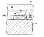
以下、本実施の形態に係る電球形ランプ1の特徴について、図6を用いて説明する。図6は、本発明の実施の形態に係る電球形ランプの要部拡大断面図(図3の破線Aで囲まれる領域の拡大図)である。  Hereinafter, the characteristics of the light bulb shapedlamp 1 according to the present embodiment will be described with reference to FIG. FIG. 6 is an enlarged cross-sectional view of an essential part of the light bulb shaped lamp according to the embodiment of the present invention (enlarged view of a region surrounded by a broken line A in FIG. 3).

第1筐体60の線膨張係数と第2筐体70の線膨張係数とが異なっている場合、温度変化によって、第1筐体60及び第2筐体70にクラック(割れ)が発生するという問題がある。  When the linear expansion coefficient of thefirst casing 60 and the linear expansion coefficient of thesecond casing 70 are different, cracks are generated in thefirst casing 60 and thesecond casing 70 due to temperature changes. There's a problem.

特に、LED電球が低温環境下で使用される場合に、クラックが生じやすい。この原因の一つとして、LED電球は常温で設計されるということがある。  In particular, cracks are likely to occur when the LED bulb is used in a low temperature environment. One reason for this is that LED bulbs are designed at room temperature.

例えば、消灯状態であっても低温環境下にあるLED電球では、低温による部材の熱収縮差によってクラックが発生する。これは、同一温度では外側の部材の方が内側の部材よりも熱収縮するからである。特に、LED電球が寒冷環境下で使用される場合は、より顕著にクラックが発生する。  For example, in an LED bulb that is in a low temperature environment even in a light-off state, a crack is generated due to a difference in thermal contraction of the member due to the low temperature. This is because at the same temperature, the outer member shrinks more than the inner member. In particular, when the LED bulb is used in a cold environment, cracks are more prominent.

具体的には、本実施の形態のように、第1筐体60が金属製で、外郭をなす第2筐体70が樹脂製であって第1筐体60の外周面と第2筐体70の内周面とが面接触しているような場合、低温によって第1筐体60及び第2筐体70が熱収縮(体積収縮)すると、樹脂製の第2筐体70の方が金属製の第1筐体60よりも線膨張係数が数倍も高いことから、第1筐体60と第2筐体70との熱収縮差によって樹脂製の第2筐体70に応力歪みが生じてクラックが発生する。仮に、第1筐体60と第2筐体70との間に寸法公差程度の隙間があったとしても、第1筐体60と第2筐体70との熱収縮差を吸収することができない。なお、第1筐体60及び第2筐体70が熱収縮する方向は、第1筐体60(第2筐体70)の外周面に対して垂直な方向(紙面左右方向)が支配的となる。  Specifically, as in the present embodiment, thefirst casing 60 is made of metal, and thesecond casing 70 forming the outer shell is made of resin, and the outer peripheral surface of thefirst casing 60 and the second casing When thefirst casing 60 and thesecond casing 70 are thermally shrunk (volume contraction) at a low temperature when the inner peripheral surface of the 70 is in surface contact, the resin-madesecond casing 70 is more metallic. Since the linear expansion coefficient is several times higher than that of thefirst housing 60 made of a resin, stress distortion occurs in thesecond housing 70 made of resin due to a difference in thermal contraction between thefirst housing 60 and thesecond housing 70. Cracks. Even if there is a gap of about dimensional tolerance between thefirst housing 60 and thesecond housing 70, the thermal contraction difference between thefirst housing 60 and thesecond housing 70 cannot be absorbed. . Note that the direction in which thefirst casing 60 and thesecond casing 70 contract by heat is predominantly the direction perpendicular to the outer peripheral surface of the first casing 60 (second casing 70) (the left-right direction on the paper). Become.

また、低温環境下で点灯状態のLED電球は、LEDモジュール20及び駆動回路40から熱が発生するので、内側に存在する金属製の第1筐体60は高温となるが、外側に存在する樹脂製の第2筐体70は外気(冷気)に曝されるので低温となる。この場合、内側の金属製の第1筐体60のみが熱膨張(体積膨張)することになるので、第1筐体60の外周面と第2筐体70の内周面とが面接触していると、第1筐体60と第2筐体70との熱膨張差によって樹脂製の第2筐体70に応力歪みが生じてクラックが発生する。仮に、第1筐体60と第2筐体70との間に寸法公差程度の隙間があったとしても、第1筐体60と第2筐体70との熱膨張差を吸収することができない。なお、第1筐体60及び第2筐体70が熱膨張する方向は、熱収縮する方向と同様に、第1筐体60(第2筐体70)の外周面に対して垂直な方向(紙面左右方向)が支配的となる。  In addition, since the LED bulb that is lit in a low temperature environment generates heat from theLED module 20 and thedrive circuit 40, the metalfirst housing 60 that is present on the inside is hot, but the resin that is present on the outside. Since thesecond housing 70 is exposed to the outside air (cold air), the temperature becomes low. In this case, only the inner metalfirst housing 60 thermally expands (volume expansion), so that the outer peripheral surface of thefirst housing 60 and the inner peripheral surface of thesecond housing 70 are in surface contact. In this case, a stress distortion occurs in the resin-madesecond housing 70 due to a difference in thermal expansion between thefirst housing 60 and thesecond housing 70, and a crack is generated. Even if there is a gap of about dimensional tolerance between thefirst casing 60 and thesecond casing 70, the difference in thermal expansion between thefirst casing 60 and thesecond casing 70 cannot be absorbed. . The direction in which thefirst casing 60 and thesecond casing 70 thermally expand is the direction perpendicular to the outer peripheral surface of the first casing 60 (second casing 70), similarly to the direction in which heat contracts. The left and right direction on the paper becomes dominant.

特に、低温環境下でLED電球を点灯させたり消灯させたりすると、点灯時又は消灯時では温度変化が大きいので、第2筐体70にクラックが生じやすい。例えば、点灯中のLEDランプを消灯させると、外郭をなす第2筐体70が内側の第1筐体60よりも先に急激に冷却されるので、第2筐体70にクラックが生じやすい。  In particular, when the LED bulb is turned on or off in a low temperature environment, thesecond housing 70 is likely to crack because the temperature change is large at the time of turning on or off. For example, when the LED lamp that is turned on is turned off, thesecond casing 70 that forms the outer shell is rapidly cooled before the innerfirst casing 60, so that thesecond casing 70 is likely to crack.

このように、LED電球が低温環境下にあると、樹脂製の第2筐体70にクラックが発生しやすい。  Thus, when the LED bulb is in a low temperature environment, cracks are likely to occur in thesecond housing 70 made of resin.

一方、LED電球が低温環境下にない場合であっても、第1筐体60と第2筐体70とが接着等によって固定されていると、第2筐体70にクラックが発生する。例えば、LED電球が高温環境下にある場合は、高温によって接着状態の第1筐体60及び第2筐体70が熱膨張(体積膨張)するので、第1筐体60と第2筐体70との熱膨張差によって樹脂製の第2筐体70に応力歪みが生じてクラックが発生する。あるいは、LED電球が常温下にある場合であっても、点灯状態のLED電球では、LEDモジュール20及び駆動回路40から熱が発生する。この熱によって第1筐体60及び第2筐体70が接着状態で熱膨張(体積膨張)するので、第1筐体60と第2筐体70との熱膨張差によって第2筐体70にクラックが発生する。  On the other hand, even if the LED bulb is not in a low temperature environment, if thefirst housing 60 and thesecond housing 70 are fixed by adhesion or the like, a crack occurs in thesecond housing 70. For example, when the LED bulb is in a high temperature environment, thefirst casing 60 and thesecond casing 70 in the bonded state are thermally expanded (volume expansion) due to the high temperature, and thus thefirst casing 60 and thesecond casing 70 are heated. Due to the difference in thermal expansion, stress strain occurs in thesecond housing 70 made of resin, and cracks occur. Alternatively, even when the LED bulb is at room temperature, heat is generated from theLED module 20 and thedrive circuit 40 in the LED bulb that is lit. This heat causes thefirst housing 60 and thesecond housing 70 to thermally expand (volume expansion) in the bonded state, and therefore, due to the difference in thermal expansion between thefirst housing 60 and thesecond housing 70, Cracks occur.

そこで、本実施の形態における電球形ランプ1では、第1筐体60と第2筐体70との間に、第1筐体60及び第2筐体70の体積膨張(熱膨張)や体積収縮(熱収縮)を吸収するための物理的な隙間(空気層)が存在するようにして、第1筐体60と第2筐体70とを配置している。本実施の形態では、第2筐体70の内径を第1筐体60の外径よりも大きくすることで、第1筐体60の外周面と第2筐体70の内周面との間に隙間(クリアランス)を設けている。このように、第1筐体60と第2筐体70との間の隙間は、第1筐体60(第2筐体70)が熱膨張(熱収縮)しやすい方向に設けられている。  Therefore, in the light bulb shapedlamp 1 according to the present embodiment, the volume expansion (thermal expansion) or volume contraction of thefirst casing 60 and thesecond casing 70 is between thefirst casing 60 and thesecond casing 70. Thefirst housing 60 and thesecond housing 70 are arranged so that there is a physical gap (air layer) for absorbing (heat shrinkage). In the present embodiment, by making the inner diameter of thesecond housing 70 larger than the outer diameter of thefirst housing 60, the space between the outer peripheral surface of thefirst housing 60 and the inner peripheral surface of thesecond housing 70 is increased. Is provided with a clearance. As described above, the gap between thefirst casing 60 and thesecond casing 70 is provided in a direction in which the first casing 60 (second casing 70) is likely to thermally expand (heat contract).

これにより、線膨張係数の異なる第1筐体60と第2筐体70とが熱膨張又は熱収縮したとしても、第1筐体60と第2筐体70との熱膨張差又は熱収縮差を当該隙間によって吸収することができる。これにより、第2筐体70にクラックが発生することを抑制することができる。  Thereby, even if thefirst casing 60 and thesecond casing 70 having different linear expansion coefficients are thermally expanded or contracted, the difference in thermal expansion or the difference between thefirst casing 60 and thesecond casing 70 is caused. Can be absorbed by the gap. Thereby, it can suppress that a crack generate | occur | produces in the 2nd housing | casing 70. FIG.

なお、本実施の形態において、第1筐体60の外周面と第2筐体70の内周面との一部は接触していても構わない。例えば、第1筐体60と第2筐体70との中心軸がずれて第1筐体60の外周面と第2筐体70の内周面の一部が接触していても構わない。この場合、接触している箇所の反対側には隙間が存在することになる。このように、第1筐体60の外周面と第2筐体70の内周面との間のどこかに隙間が設けられていればよい。ただし、第1筐体60の外周面と第2筐体70の内周面とは、全域において非接触であることが好ましい。  In the present embodiment, a part of the outer peripheral surface of thefirst housing 60 and the inner peripheral surface of thesecond housing 70 may be in contact with each other. For example, the central axes of thefirst housing 60 and thesecond housing 70 may be shifted so that the outer peripheral surface of thefirst housing 60 and a part of the inner peripheral surface of thesecond housing 70 are in contact with each other. In this case, a gap exists on the opposite side of the contacted portion. Thus, it is sufficient that a gap is provided somewhere between the outer peripheral surface of thefirst housing 60 and the inner peripheral surface of thesecond housing 70. However, it is preferable that the outer peripheral surface of thefirst housing 60 and the inner peripheral surface of thesecond housing 70 are not in contact with each other.

また、本実施の形態において、第1筐体60は、当該第1筐体60の円筒部材の内方に向かって折れ曲がるように設けられた屈曲部60aを有する。第1筐体60の屈曲部60aは、第1筐体60の円筒部材の口金側の開口端部に設けられている。さらに、第2筐体70も、当該第2筐体70の円筒部材の内方に向かって折れ曲がるように設けられた屈曲部70aを有する。さらに、回路ケース50も、当該回路ケース50の円筒部材の内方に向かって折れ曲がるように設けられた屈曲部50aを有する。屈曲部50a、屈曲部60a及び屈曲部70aの主面垂直方向は、いずれもランプ軸Jと平行であり、屈曲部60aは、屈曲部50aと屈曲部70aとによって挟持されている。  Further, in the present embodiment, thefirst housing 60 has abent portion 60 a provided so as to be bent inward of the cylindrical member of thefirst housing 60. Thebent portion 60 a of thefirst housing 60 is provided at the opening end on the base side of the cylindrical member of thefirst housing 60. Furthermore, thesecond housing 70 also has abent portion 70 a provided so as to be bent inward of the cylindrical member of thesecond housing 70. Further, thecircuit case 50 also has abent portion 50 a provided so as to be bent inward of the cylindrical member of thecircuit case 50. The principal surface perpendicular directions of thebent portion 50a, thebent portion 60a, and thebent portion 70a are all parallel to the lamp axis J, and thebent portion 60a is sandwiched between thebent portion 50a and thebent portion 70a.

これにより、第1筐体60の屈曲部60aの外面と第2筐体70の屈曲部70aの内面とを接触させることができる。このため、第1筐体60に伝導したLEDモジュール20の熱を効率良く第2筐体70に伝導させることができるので、LEDモジュール20の放熱性を向上させることができる。  Thereby, the outer surface of the bendingpart 60a of the 1st housing | casing 60 and the inner surface of the bendingpart 70a of the 2nd housing | casing 70 can be made to contact. For this reason, since the heat of theLED module 20 conducted to thefirst housing 60 can be efficiently conducted to thesecond housing 70, the heat dissipation of theLED module 20 can be improved.

このように、屈曲部60aと屈曲部70aとを接触させることで、第2筐体70のクラックを防止するだけではなく、放熱性にも優れた電球形ランプを実現することができる。  In this way, by bringing thebent portion 60a and thebent portion 70a into contact with each other, it is possible not only to prevent cracks in thesecond housing 70 but also to realize a light bulb shaped lamp that is excellent in heat dissipation.

なお、第1筐体60(第2筐体70)が熱膨張(熱収縮)する方向は、上述のとおり、第1筐体60(第2筐体70)の外周面に対して垂直な方向(ランプ軸Jと直交する方向)が支配的となり、屈曲部60aと屈曲部70aとの接触面における法線は、熱膨張(熱収縮)が支配的ではないランプ軸Jと平行な方向である。したがって、第1筐体60と第2筐体70とを屈曲部60a及び屈曲部70aの位置で接触させたとしても、第2筐体70にクラックは発生しない。  The direction in which the first casing 60 (second casing 70) thermally expands (thermal contraction) is a direction perpendicular to the outer peripheral surface of the first casing 60 (second casing 70) as described above. (The direction orthogonal to the lamp axis J) becomes dominant, and the normal line at the contact surface between thebent portion 60a and thebent portion 70a is a direction parallel to the lamp axis J where thermal expansion (thermal contraction) is not dominant. . Therefore, even if thefirst housing 60 and thesecond housing 70 are brought into contact with each other at the positions of thebent portion 60a and thebent portion 70a, no cracks are generated in thesecond housing 70.

また、第1筐体60の外周面と第2筐体70の内周面との間の隙間は、ランプ点灯時の温度と第1筐体60及び第2筐体70の線膨張係数とを考慮すると、少なくとも0.1mm以上とすることが好ましい。より好ましくは、第1筐体60の外周面と第2筐体70の内周面との間の隙間は、0.15mm程度以上である。これは、LED電球程度のスケールであれば、常温環境から低温環境への温度変化の場合、外郭をなす樹脂製の第2筐体70は、内側の金属製の第1筐体60よりも径が0.15mm程度収縮するからである。  Further, the gap between the outer peripheral surface of thefirst housing 60 and the inner peripheral surface of thesecond housing 70 determines the temperature at the time of lamp lighting and the linear expansion coefficients of thefirst housing 60 and thesecond housing 70. Considering it, it is preferable to set it to at least 0.1 mm or more. More preferably, the gap between the outer peripheral surface of thefirst housing 60 and the inner peripheral surface of thesecond housing 70 is about 0.15 mm or more. If this is a scale similar to that of an LED bulb, the resin-madesecond housing 70 that forms the outer shell has a diameter larger than the inner metal-madefirst housing 60 in the case of a temperature change from a normal temperature environment to a low temperature environment. Is about 0.15 mm.

また、本実施の形態では、第1筐体60と第2筐体70との間だけではなく、第1筐体60の内周面と回路ケース50の外周面との間にも、第1筐体60及び回路ケース50の体積膨張(熱膨張)や体積収縮(熱収縮)を吸収するための所定の隙間が設けられている。これにより、線膨張係数の異なる金属製の第1筐体60と樹脂製の回路ケース50(ケース本体部51)とが熱膨張又は熱収縮したとしても、第1筐体60と回路ケース50との熱膨張差又は熱収縮差を当該隙間によって吸収することができる。これにより、第2筐体70にクラックが発生することを抑制することができる。  In the present embodiment, not only between thefirst housing 60 and thesecond housing 70 but also between the inner peripheral surface of thefirst housing 60 and the outer peripheral surface of thecircuit case 50. A predetermined gap for absorbing volume expansion (thermal expansion) and volume contraction (thermal contraction) of thehousing 60 and thecircuit case 50 is provided. As a result, even if the metalfirst housing 60 and the resin circuit case 50 (case body 51) having different linear expansion coefficients thermally expand or contract, thefirst housing 60 and thecircuit case 50 The thermal expansion difference or thermal contraction difference can be absorbed by the gap. Thereby, it can suppress that a crack generate | occur | produces in the 2nd housing | casing 70. FIG.

また、本実施の形態において、第1筐体60と第2筐体70との間の隙間(第1の隙間)は、第1筐体60と回路ケース50との間の隙間(第2の隙間)よりも小さい。すなわち、第1筐体60と第2筐体70との間の隙間の距離d1は、第1筐体60と回路ケース50(ケース本体部51)との間の隙間の距離d2よりも小さくなっている。これにより、第1筐体60と第2筐体70との間における熱伝導性を向上させつつ、第1筐体60と回路ケース50との間における熱伝導性を低下させることができる。この結果、駆動回路40で発生した熱の放熱経路とLEDモジュール20で発生した熱の放熱経路とを分けることができる。したがって、LEDモジュール20で発生した熱は、第1筐体60を介して第2筐体70に効率良く伝導させることができる。一方、駆動回路40で発生した熱は、主に、第1筐体60ではなく、口金80の方へと伝導させることができる。  In the present embodiment, the gap between the
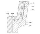
first casing 60 and the second casing 70 (first gap) is the gap between thefirst casing 60 and the circuit case 50 (second gap). Smaller than the gap). That is, the gap distance d1 between thefirst housing 60 and thesecond housing 70 is smaller than the gap distance d2 between thefirst housing 60 and the circuit case 50 (case body 51). ing. Thereby, the thermal conductivity between the 1st housing | casing 60 and thecircuit case 50 can be reduced, improving the thermal conductivity between the 1st housing | casing 60 and the 2nd housing | casing 70. FIG. As a result, the heat radiation path of the heat generated in thedrive circuit 40 and the heat radiation path of the heat generated in theLED module 20 can be separated. Therefore, the heat generated in theLED module 20 can be efficiently conducted to thesecond housing 70 via thefirst housing 60. On the other hand, the heat generated in thedrive circuit 40 can be mainly conducted not to thefirst housing 60 but to thebase 80.

(変形例1)
次に、本実施の形態の変形例1について、図7を用いて説明する。図7は、本発明の実施の形態の変形例1に係る電球形ランプの要部拡大断面図である。
(Modification 1)
Next,Modification 1 of the present embodiment will be described with reference to FIG. FIG. 7 is an enlarged cross-sectional view of a main part of a light bulb shaped lamp according to a first modification of the embodiment of the present invention.

図7に示すように、本変形例に係る電球形ランプは、上記の実施の形態における電球形ランプ1に対して、さらに、第1筐体60の屈曲部60aに孔部60a1が形成されているとともに、第2筐体70の屈曲部70aに凸部70a1が形成されている。  As shown in FIG. 7, the light bulb shaped lamp according to the present modification has ahole 60 a 1 formed in thebent portion 60 a of thefirst housing 60 in addition to the light bulb shapedlamp 1 in the above embodiment. In addition, aconvex portion 70 a 1 is formed on thebent portion 70 a of thesecond housing 70.

本変形例では、孔部60a1と凸部70a1とが嵌合するように構成されており、第1筐体60と第2筐体70とを組み合わせるときに、凸部70a1を孔部60a1に嵌合させることによって、第2筐体70に対する第1筐体60の位置を決定することができる。これにより、孔部60a1と凸部70a1とによって第1筐体60と第2筐体70との相対的な位置関係を決めることができる。  In this modification, the hole 60a1 and the protrusion 70a1 are configured to be fitted together, and when thefirst casing 60 and thesecond casing 70 are combined, the protrusion 70a1 is fitted into the hole 60a1. By combining, the position of thefirst housing 60 with respect to thesecond housing 70 can be determined. Thereby, the relative positional relationship between thefirst housing 60 and thesecond housing 70 can be determined by the hole 60a1 and the convex portion 70a1.

この結果、第1筐体60と第2筐体70との間の隙間が所定の間隔となるように、精度良く第1筐体60と第2筐体70とを配置することができる。また、第1筐体60と回路ケース50との間の隙間が所定の間隔となるように、精度良く第1筐体60と回路ケース50とを配置することもできる。  As a result, thefirst casing 60 and thesecond casing 70 can be arranged with high accuracy so that the gap between thefirst casing 60 and thesecond casing 70 becomes a predetermined interval. In addition, thefirst casing 60 and thecircuit case 50 can be arranged with high accuracy so that the gap between thefirst casing 60 and thecircuit case 50 is a predetermined interval.

(変形例2)
次に、本実施の形態の変形例2について、図8を用いて説明する。図8は、本発明の実施の形態の変形例2に係る電球形ランプの要部拡大断面図である。
(Modification 2)
Next, Modification Example 2 of the present embodiment will be described with reference to FIG. FIG. 8 is an enlarged cross-sectional view of a main part of a light bulb shaped lamp according to a second modification of the embodiment of the present invention.

図8に示すように、本変形例に係る電球形ランプは、上記の実施の形態における電球形ランプ1に対して、さらに、第1筐体60に弾力性を有する爪部61が形成されている。爪部61は、金属製の第1筐体60の一部を切り欠いて、第2筐体70の内周面に向かって屈曲させることで構成することができる。本変形例において、爪部61の先端部は、第2筐体70の内周面に当接している。  As shown in FIG. 8, the light bulb shaped lamp according to the present modified example is further provided with aclaw portion 61 having elasticity in thefirst housing 60 compared to the light bulb shapedlamp 1 in the above embodiment. Yes. Theclaw portion 61 can be configured by cutting out a part of the metalfirst casing 60 and bending it toward the inner peripheral surface of thesecond casing 70. In this modification, the tip of theclaw 61 is in contact with the inner peripheral surface of thesecond housing 70.

このように、爪部61を設けることによって、第1筐体60の外周面と第2筐体70の内周面との間に隙間を設けつつ、第1筐体60の一部を第2筐体70の内周面に接触させることができる。  As described above, by providing theclaw portion 61, a part of thefirst housing 60 is made to be the second while providing a gap between the outer peripheral surface of thefirst housing 60 and the inner peripheral surface of thesecond housing 70. The inner peripheral surface of thehousing 70 can be contacted.

これにより、線膨張係数の異なる第1筐体60と第2筐体70とが熱膨張したとしても、爪部61が弾性力を有するので、第1筐体60と第2筐体70との接触状態を維持しつつ、第1筐体60と第2筐体70との熱膨張差又は熱収縮差を、上記隙間によって吸収することができる。  Thereby, even if thefirst casing 60 and thesecond casing 70 having different linear expansion coefficients thermally expand, theclaw portion 61 has an elastic force, so that thefirst casing 60 and thesecond casing 70 While maintaining the contact state, the thermal expansion difference or thermal contraction difference between thefirst casing 60 and thesecond casing 70 can be absorbed by the gap.

したがって、第2筐体70のクラックを防止するだけではなく、放熱性にも優れた電球形ランプを実現することができる。  Therefore, it is possible to realize a light bulb shaped lamp that not only prevents cracking of thesecond housing 70 but also has excellent heat dissipation.

(照明装置)
また、本発明は、このような電球形ランプとして実現することができるだけでなく、電球形ランプを備える照明装置としても実現することができる。以下、本発明の実施の形態に係る照明装置について、図9を用いて説明する。図9は、本発明の実施の形態に係る照明装置の概略断面図である。
(Lighting device)
Further, the present invention can be realized not only as such a light bulb shaped lamp but also as an illumination device including a light bulb shaped lamp. Hereinafter, a lighting device according to an embodiment of the present invention will be described with reference to FIG. FIG. 9 is a schematic cross-sectional view of the illumination device according to the embodiment of the present invention.

図9に示すように、本発明の実施の形態に係る照明装置2は、例えば、室内の天井に装着されて使用され、上記の実施の形態に係る電球形ランプ1と、点灯器具3とを備える。  As shown in FIG. 9, thelighting device 2 according to the embodiment of the present invention is used, for example, mounted on an indoor ceiling, and includes the light bulb shapedlamp 1 according to the above embodiment and thelighting fixture 3. Prepare.

点灯器具3は、電球形ランプ1を消灯及び点灯させるものであり、天井に取り付けられる器具本体4と、電球形ランプ1を覆う透光性のランプカバー5とを備える。  Thelighting device 3 turns off and turns on the light bulb shapedlamp 1 and includes a devicemain body 4 attached to the ceiling and a translucent lamp cover 5 that covers the light bulb shapedlamp 1.

器具本体4は、ソケット4aを有する。ソケット4aには、電球形ランプ1の口金80がねじ込まれる。このソケット4aを介して電球形ランプ1に電力が供給される。  Theinstrument body 4 has asocket 4a. Abase 80 of the light bulb shapedlamp 1 is screwed into thesocket 4a. Electric power is supplied to the light bulb shapedlamp 1 through thesocket 4a.

(その他)
以上、本発明に係る電球形ランプ及び照明装置について、実施の形態及び変形例に基づいて説明したが、本発明は、これらの実施の形態に限定されるものではない。
(Other)
As described above, the light bulb shaped lamp and the lighting device according to the present invention have been described based on the embodiments and the modified examples. However, the present invention is not limited to these embodiments.

例えば、上記の実施の形態及び変形例において、LEDモジュール20は基台21上にLEDチップを直接実装したCOB型の構成としたが、これに限らない。例えば、樹脂製の容器の凹部(キャビティ)の中にLEDチップ(発光素子)を実装して当該凹部内に封止部材(蛍光体含有樹脂)を封入したパッケージ型のLED素子(SMD型LED素子)を用いて、このLED素子を金属配線が形成された基台21上に複数個実装することで構成されたSMD型のLEDモジュールを用いても構わない。  For example, in the above-described embodiment and modification, theLED module 20 has a COB type configuration in which the LED chip is directly mounted on thebase 21, but is not limited thereto. For example, a package type LED element (SMD type LED element) in which an LED chip (light emitting element) is mounted in a recess (cavity) of a resin container and a sealing member (phosphor-containing resin) is enclosed in the recess ), An SMD type LED module configured by mounting a plurality of the LED elements on thebase 21 on which the metal wiring is formed may be used.

また、上記の実施の形態及び変形例において、LEDモジュール20の基台21としては、1枚の白色基板を用いたが、表面にLED22及び封止部材23を形成した2枚の白色基板の裏側の面同士を貼り合わせることで、1つのLEDモジュール20を構成しても構わない。  In the above-described embodiment and modification, one white substrate is used as thebase 21 of theLED module 20, but the back side of the two white substrates having theLED 22 and the sealingmember 23 formed on the surface thereof. Asingle LED module 20 may be configured by bonding the two surfaces together.

また、上記の実施の形態及び変形例において、LEDモジュール20は、青色LEDチップと黄色蛍光体とによって白色光を放出するように構成したが、これに限らない。例えば、演色性を高めるために、黄色蛍光体に加えて、さらに赤色蛍光体や緑色蛍光体を混ぜても構わない。また、黄色蛍光体を用いずに、赤色蛍光体及び緑色蛍光体を含有する蛍光体含有樹脂を用いて、これと青色LEDチップとを組み合わせることによりに白色光を放出するように構成することもできる。  Moreover, in said embodiment and modification, although theLED module 20 was comprised so that a white light might be emitted by a blue LED chip and a yellow fluorescent substance, it is not restricted to this. For example, in order to improve color rendering properties, a red phosphor or a green phosphor may be further mixed in addition to the yellow phosphor. Moreover, it is also possible to use a phosphor-containing resin containing a red phosphor and a green phosphor without using a yellow phosphor, and to emit white light by combining this with a blue LED chip. it can.

また、上記の実施の形態及び変形例において、LEDチップは、青色以外の色を発光するLEDチップを用いても構わない。例えば、紫外線発光のLEDチップを用いる場合、蛍光体粒子としては、三原色(赤色、緑色、青色)に発光する各色蛍光体粒子を組み合わせたものを用いることができる。さらに、蛍光体粒子以外の波長変換材を用いてもよく、例えば、波長変換材として、半導体、金属錯体、有機染料、顔料など、ある波長の光を吸収し、吸収した光とは異なる波長の光を発する物質を含んでいる材料を用いてもよい。  Moreover, in said embodiment and modification, you may use the LED chip which light-emits colors other than blue as an LED chip. For example, when an ultraviolet light emitting LED chip is used, a combination of phosphor particles that emit light in three primary colors (red, green, and blue) can be used as the phosphor particles. Furthermore, a wavelength conversion material other than the phosphor particles may be used. For example, the wavelength conversion material absorbs light of a certain wavelength such as a semiconductor, a metal complex, an organic dye, or a pigment, and has a wavelength different from the absorbed light. A material containing a substance that emits light may be used.

また、上記の実施の形態及び変形例において、発光素子としてLEDを例示したが、半導体レーザ等の半導体発光素子、有機EL(Electro Luminescence)又は無機EL等の発光素子を用いてもよい。  Further, in the above embodiments and modifications, the LED is exemplified as the light emitting element, but a semiconductor light emitting element such as a semiconductor laser, a light emitting element such as an organic EL (Electro Luminescence), or an inorganic EL may be used.

その他、各実施の形態に対して当業者が思いつく各種変形を施して得られる形態、又は、本発明の趣旨を逸脱しない範囲で各実施の形態における構成要素及び機能を任意に組み合わせることで実現される形態も本発明に含まれる。  In addition, the present invention can be realized by various combinations conceived by those skilled in the art for each embodiment, or by arbitrarily combining the components and functions in each embodiment without departing from the spirit of the present invention. This form is also included in the present invention.

本発明は、従来の白熱電球等を代替する電球形ランプとして有用であり、照明装置等において広く利用することができる。  INDUSTRIAL APPLICABILITY The present invention is useful as a light bulb shaped lamp that replaces a conventional incandescent light bulb and the like, and can be widely used in lighting devices and the like.

1 電球形ランプ
2 照明装置
3 点灯器具
4 器具本体
4a ソケット
5 ランプカバー
10 グローブ
11 開口部
20 LEDモジュール
21 基台
22 LED
22a サファイア基板
22b 窒化物半導体層
22c カソード電極
22d アノード電極
22e、22f ワイヤーボンド部
22g チップボンディング材
23 封止部材
24 金属配線
25 ワイヤー
26a、26b 端子
27、28a、28b 貫通孔
30 支持部材
31 支柱
32 台座
32a 径小部
32b 径大部
40 駆動回路
41 回路基板
42 回路素子
43a、43b、43c、43d リード線
50 回路ケース
50a、60a、70a 屈曲部
51 ケース本体部
51a 第1ケース部
51b 第2ケース部
52 キャップ部
60 第1筐体
60a1 孔部
61 爪部
70 第2筐体
70a1 凸部
80 口金
81 シェル部
82 絶縁部
83 アイレット部
90 ネジ
DESCRIPTION OFSYMBOLS 1 Light bulb shapedlamp 2Illuminating device 3Lighting fixture 4 Appliancemain body 4a Socket 5Lamp cover 10Globe 11Opening 20LED module 21Base 22 LED
22a Sapphire substrate 22bNitride semiconductor layer 22c Cathode electrode22d Anode electrode 22e, 22f Wire bond part 22gChip bonding material 23 Sealingmember 24Metal wiring 25Wire 26a,26b Terminal 27, 28a, 28b Throughhole 30Support member 31Support column 31Pedestal 32aSmall diameter part 32bLarge diameter part 40Drive circuit 41Circuit board 42Circuit element 43a, 43b, 43c,43d Lead wire 50Circuit case 50a, 60a,70a Bent part 51Case body part 51aFirst case part 51bSecond case Part 52Cap part 60 1st housing |casing 60a1 Hole 61Claw part 70 2nd housing | casing70a1 Convex part 80Base 81 Shell part 82 Insulatingpart 83Eyelet part 90 Screw

Claims (5)

Translated fromJapanese
発光モジュールと、
前記発光モジュールを発光させるための駆動回路と、
前記駆動回路を囲むように構成された金属製の第1筐体と、
前記第1筐体を囲むように構成されるとともに外郭をなす樹脂製の第2筐体と、
前記第1筐体の内側に配置されるとともに前記駆動回路を囲むように構成された回路ケースと、を備え、
前記第2筐体の線膨張係数は、前記第1筐体の線膨張係数よりも大きく、
前記第1筐体と前記第2筐体との間には隙間が設けられており、
前記第1筐体と前記回路ケースとの間には隙間が設けられており、
前記回路ケースの外周面には、口金と螺合するための螺合部が形成されており、
前記第1筐体、前記第2筐体及び前記回路ケースの各々は、円筒部材であり、
前記第1筐体、前記第2筐体及び前記回路ケースの各々は、前記円筒部材の内方に向かって折れ曲がるように設けられた屈曲部を有し、
前記第1筐体の前記屈曲部の外面と前記第2筐体の前記屈曲部の内面とが接触しており、かつ、前記回路ケースの前記屈曲部の外面と前記第1筐体の前記屈曲部の内面とが接触している
照明用光源。
A light emitting module;
A driving circuit for causing the light emitting module to emit light;
Ametal first housing configured to surround the drive circuit;
A second housingmade of resin and surrounding the first housing;
A circuit case disposed inside the first housing and configured to surround the drive circuit ,
The linear expansion coefficient of the second housing is larger than the linear expansion coefficient of the first housing,
A gap is provided between the first housing and the second housing,
A gap is provided between the first housing and the circuit case,
The outer peripheral surface of the circuit case is formed with a screwing portion for screwing with the base,
Each of the first housing, the second housing, and the circuit case is a cylindrical member,
Each of the first housing, the second housing, and the circuit case has a bent portion that is provided so as to be bent inward of the cylindrical member;
The outer surface of the bent portion of the first housing is in contact with the inner surface of the bent portion of the second housing, and the outer surface of the bent portion of the circuit case and the bent of the first housing. Illumination light source incontact with the inner surface of the part .
記隙間は、前記第1筐体の外周面と前記第2筐体の内周面との間に設けられている
請求項1に記載の照明用光源。
Before SL gap, the illumination light source according to claim 1 is provided between the outer surface and the inner peripheral surface of the second housing of the first housing.
前記第1筐体と前記第2筐体との間の隙間は、前記第1筐体と前記回路ケースとの間の隙間よりも小さい
請求項に記載の照明用光源。
The gap between the first housing and the second housing, the illumination light source according to claim1 smaller than the gap between the first housing and the circuit case.
さらに、前記発光モジュールを支持する支持部材を備え、
前記第1筐体は、前記支持部材と接触している
請求項1〜のいずれか1項に記載の照明用光源。
Furthermore, a support member for supporting the light emitting module is provided,
Said first housing, the illumination light source according to any one of claims 1 to3 in contact with the support member.
請求項1〜のいずれか1項に記載の照明用光源を備える
照明装置。
An illumination device comprising the illumination light source according to any one of claims 1 to4 .
JP2012256695A2012-11-222012-11-22 Illumination light source and illumination deviceActiveJP5948666B2 (en)

Priority Applications (1)

Application NumberPriority DateFiling DateTitle
JP2012256695AJP5948666B2 (en)2012-11-222012-11-22 Illumination light source and illumination device

Applications Claiming Priority (1)

Application NumberPriority DateFiling DateTitle
JP2012256695AJP5948666B2 (en)2012-11-222012-11-22 Illumination light source and illumination device

Publications (2)

Publication NumberPublication Date
JP2014107022A JP2014107022A (en)2014-06-09
JP5948666B2true JP5948666B2 (en)2016-07-06

Family

ID=51028359

Family Applications (1)

Application NumberTitlePriority DateFiling Date
JP2012256695AActiveJP5948666B2 (en)2012-11-222012-11-22 Illumination light source and illumination device

Country Status (1)

CountryLink
JP (1)JP5948666B2 (en)

Families Citing this family (2)

* Cited by examiner, † Cited by third party
Publication numberPriority datePublication dateAssigneeTitle
JP6788860B2 (en)2016-08-232020-11-25パナソニックIpマネジメント株式会社 Light emitting device and lighting device
KR102450579B1 (en)*2017-06-052022-10-07삼성전자주식회사Led lamp

Family Cites Families (3)

* Cited by examiner, † Cited by third party
Publication numberPriority datePublication dateAssigneeTitle
JP4569465B2 (en)*2005-04-082010-10-27東芝ライテック株式会社 lamp
US8471443B2 (en)*2009-11-092013-06-25Lg Innotek Co., Ltd.Lighting device
TWM391052U (en)*2010-04-272010-10-21Advanced Connectek IncHeat dissipation auxiliary device for lamp

Also Published As

Publication numberPublication date
JP2014107022A (en)2014-06-09

Similar Documents

PublicationPublication DateTitle
JP5830668B2 (en) Light emitting device and light source for illumination
JPWO2014010141A1 (en) Light bulb shaped lamp and lighting device
JP2014157691A (en)Light emitting device and light source for lighting
JP5948666B2 (en) Illumination light source and illumination device
JP6176572B2 (en) Illumination light source and illumination device
JP6098928B2 (en) Illumination light source and illumination device
JP5967483B2 (en) Light source for illumination
JPWO2014013671A1 (en) Light bulb shaped lamp and lighting device
JP5588569B2 (en) Light bulb shaped lamp and lighting device
JP5420124B1 (en) Light bulb shaped lamp, lighting device, and method of manufacturing light bulb shaped lamp
JP5793721B2 (en) Illumination light source and illumination device
JP5563730B1 (en) Illumination light source and illumination device
JP6225397B2 (en) Illumination light source and illumination device
JP6191813B2 (en) Illumination light source and illumination device
JP5417556B1 (en) Light bulb shaped lamp and lighting device
JP5493058B1 (en) Light bulb shaped lamp and lighting device
WO2014024339A1 (en)Bulb-type lamp, illumination device, and method for manufacturing bulb-type lamp
WO2014030276A1 (en)Bulb lamp and illumination device
JPWO2014010146A1 (en) Light bulb shaped lamp and lighting device
JP5433818B1 (en) Light bulb shaped lamp and lighting device
WO2014041721A1 (en)Light source for illumination and illumination device
JP2014146510A (en)Light source for lighting and lighting device
JPWO2014006790A1 (en) Light bulb shaped lamp, lighting device, and method of manufacturing light bulb shaped lamp

Legal Events

DateCodeTitleDescription
A621Written request for application examination

Free format text:JAPANESE INTERMEDIATE CODE: A621

Effective date:20150213

A711Notification of change in applicant

Free format text:JAPANESE INTERMEDIATE CODE: A711

Effective date:20150312

A977Report on retrieval

Free format text:JAPANESE INTERMEDIATE CODE: A971007

Effective date:20151118

A131Notification of reasons for refusal

Free format text:JAPANESE INTERMEDIATE CODE: A131

Effective date:20151201

A521Written amendment

Free format text:JAPANESE INTERMEDIATE CODE: A523

Effective date:20160112

TRDDDecision of grant or rejection written
A01Written decision to grant a patent or to grant a registration (utility model)

Free format text:JAPANESE INTERMEDIATE CODE: A01

Effective date:20160510

A61First payment of annual fees (during grant procedure)

Free format text:JAPANESE INTERMEDIATE CODE: A61

Effective date:20160518

R151Written notification of patent or utility model registration

Ref document number:5948666

Country of ref document:JP

Free format text:JAPANESE INTERMEDIATE CODE: R151


[8]ページ先頭

©2009-2025 Movatter.jp