JP5947263B2 - Antenna and wireless communication device - Google Patents
Antenna and wireless communication deviceDownload PDFInfo
- Publication number
- JP5947263B2 JP5947263B2JP2013175562AJP2013175562AJP5947263B2JP 5947263 B2JP5947263 B2JP 5947263B2JP 2013175562 AJP2013175562 AJP 2013175562AJP 2013175562 AJP2013175562 AJP 2013175562AJP 5947263 B2JP5947263 B2JP 5947263B2
- Authority
- JP
- Japan
- Prior art keywords
- antenna
- srr
- distance
- dummy
- conductor plate
- Prior art date
- Legal status (The legal status is an assumption and is not a legal conclusion. Google has not performed a legal analysis and makes no representation as to the accuracy of the status listed.)
- Active
Links
Images


Classifications
- H—ELECTRICITY
- H01—ELECTRIC ELEMENTS
- H01Q—ANTENNAS, i.e. RADIO AERIALS
- H01Q1/00—Details of, or arrangements associated with, antennas
- H01Q1/12—Supports; Mounting means
- H01Q1/22—Supports; Mounting means by structural association with other equipment or articles
- H01Q1/24—Supports; Mounting means by structural association with other equipment or articles with receiving set
- H01Q1/241—Supports; Mounting means by structural association with other equipment or articles with receiving set used in mobile communications, e.g. GSM
- H01Q1/242—Supports; Mounting means by structural association with other equipment or articles with receiving set used in mobile communications, e.g. GSM specially adapted for hand-held use
- H01Q1/243—Supports; Mounting means by structural association with other equipment or articles with receiving set used in mobile communications, e.g. GSM specially adapted for hand-held use with built-in antennas
- H—ELECTRICITY
- H01—ELECTRIC ELEMENTS
- H01Q—ANTENNAS, i.e. RADIO AERIALS
- H01Q1/00—Details of, or arrangements associated with, antennas
- H01Q1/12—Supports; Mounting means
- H01Q1/22—Supports; Mounting means by structural association with other equipment or articles
- H01Q1/2291—Supports; Mounting means by structural association with other equipment or articles used in bluetooth or WI-FI devices of Wireless Local Area Networks [WLAN]
- H—ELECTRICITY
- H01—ELECTRIC ELEMENTS
- H01Q—ANTENNAS, i.e. RADIO AERIALS
- H01Q1/00—Details of, or arrangements associated with, antennas
- H01Q1/36—Structural form of radiating elements, e.g. cone, spiral, umbrella; Particular materials used therewith
- H01Q1/38—Structural form of radiating elements, e.g. cone, spiral, umbrella; Particular materials used therewith formed by a conductive layer on an insulating support
- H—ELECTRICITY
- H01—ELECTRIC ELEMENTS
- H01Q—ANTENNAS, i.e. RADIO AERIALS
- H01Q1/00—Details of, or arrangements associated with, antennas
- H01Q1/48—Earthing means; Earth screens; Counterpoises
- H—ELECTRICITY
- H01—ELECTRIC ELEMENTS
- H01Q—ANTENNAS, i.e. RADIO AERIALS
- H01Q1/00—Details of, or arrangements associated with, antennas
- H01Q1/52—Means for reducing coupling between antennas; Means for reducing coupling between an antenna and another structure
- H—ELECTRICITY
- H01—ELECTRIC ELEMENTS
- H01Q—ANTENNAS, i.e. RADIO AERIALS
- H01Q1/00—Details of, or arrangements associated with, antennas
- H01Q1/52—Means for reducing coupling between antennas; Means for reducing coupling between an antenna and another structure
- H01Q1/521—Means for reducing coupling between antennas; Means for reducing coupling between an antenna and another structure reducing the coupling between adjacent antennas
- H—ELECTRICITY
- H01—ELECTRIC ELEMENTS
- H01Q—ANTENNAS, i.e. RADIO AERIALS
- H01Q19/00—Combinations of primary active antenna elements and units with secondary devices, e.g. with quasi-optical devices, for giving the antenna a desired directional characteristic
- H—ELECTRICITY
- H01—ELECTRIC ELEMENTS
- H01Q—ANTENNAS, i.e. RADIO AERIALS
- H01Q21/00—Antenna arrays or systems
- H01Q21/28—Combinations of substantially independent non-interacting antenna units or systems
- H—ELECTRICITY
- H01—ELECTRIC ELEMENTS
- H01Q—ANTENNAS, i.e. RADIO AERIALS
- H01Q9/00—Electrically-short antennas having dimensions not more than twice the operating wavelength and consisting of conductive active radiating elements
- H01Q9/04—Resonant antennas
- H01Q9/0407—Substantially flat resonant element parallel to ground plane, e.g. patch antenna
- H01Q9/0421—Substantially flat resonant element parallel to ground plane, e.g. patch antenna with a shorting wall or a shorting pin at one end of the element
Landscapes
- Engineering & Computer Science (AREA)
- Computer Networks & Wireless Communication (AREA)
- Support Of Aerials (AREA)
- Details Of Aerials (AREA)
- Waveguide Aerials (AREA)
Description
Translated fromJapanese本発明は、アンテナおよび無線通信装置に関し、特に、通信装置との無線通信に使用されるアンテナおよび無線通信装置に関する。 The present invention relates to an antenna and a wireless communication device, and more particularly to an antenna and a wireless communication device used for wireless communication with a communication device.
無線通信の普及と共に、1つの装置で複数の無線方式に対応できることが一般的になってきている。1つの装置において、時間や場所に制約されることなくいつでも様々な無線方式に対応するために、アンテナを装置内の最適な位置に配置することが求められる。また、複数の無線方式に対応するために、装置内に複数のアンテナを配置する場合もある。 With the widespread use of wireless communication, it has become common for a single device to support multiple wireless systems. In one apparatus, it is required to arrange an antenna at an optimal position in the apparatus in order to support various wireless systems at any time without being restricted by time and place. In order to support a plurality of wireless systems, a plurality of antennas may be arranged in the apparatus.
一方、携帯電話やスマートフォン等を代表とする可搬端末に対しては、高機能化に加えて小型化が要求されている。従って、装置設計においては、多数の部品を配置することが要求される。複数の無線方式に対応するためには最適な位置にアンテナを配置する必要があるが、他部品とのトレードオフの結果、アンテナを装置内の最適な位置に配置できない場合がある。 On the other hand, for portable terminals such as mobile phones and smartphones, downsizing is required in addition to high functionality. Therefore, it is required to arrange a large number of parts in the device design. In order to support a plurality of wireless systems, it is necessary to arrange the antenna at an optimal position. However, as a result of trade-off with other components, the antenna may not be arranged at an optimal position in the apparatus.
そこで、多層化プリント基板上の外周であれば、何処に実装しても良好な特性を維持できる、スプリットリング共振器(SRR:Sprit Ring Resonator)アンテナを適用することが提案されている。SRRアンテナは、例えば、特許文献1に開示されている。 Therefore, it has been proposed to apply a split ring resonator (SRR) antenna that can maintain good characteristics wherever it is mounted on the outer periphery of a multilayer printed circuit board. An SRR antenna is disclosed in
特許文献1のアンテナを図13に示す。図13に示したアンテナ900において、多層化プリント基板910の誘電体層920の上下に配置された導体層930、940の端部領域に開口931、941および切欠932、942を形成することによって、スプリットリング部951、952が形成される。そして、スプリットリング部951、952を電気的に接続する導電ビア953および、導電ビア953に接続された給電線954を誘電体層920内に配置することにより、SRRアンテナ950が形成される。 The antenna of
SRRアンテナは、多層化プリント基板上の外周であれば、何処に実装しても特性の良いアンテナとして機能する。しかし、特定の方向のアンテナ利得を得たい場合には、何処に実装しても良い訳では無い。例えば、他部品とのトレードオフの結果、SRRアンテナを天地方向の中央位置に配置できない場合は水平方向のアンテナ利得が低下することがある。さらに、SRRアンテナを装置内に複数配置した場合は、複数のSRRアンテナが干渉し合い、アイソレーションが悪化する。 The SRR antenna functions as an antenna having good characteristics wherever it is mounted on the outer periphery of the multilayer printed circuit board. However, if it is desired to obtain an antenna gain in a specific direction, it may not be installed anywhere. For example, when the SRR antenna cannot be disposed at the center position in the vertical direction as a result of trade-off with other components, the antenna gain in the horizontal direction may decrease. Further, when a plurality of SRR antennas are arranged in the apparatus, the plurality of SRR antennas interfere with each other, and isolation is deteriorated.
本発明は上記の課題に鑑みてなされたものであり、アンテナを所望の位置に配置できない場合や装置内にアンテナを複数配置した場合においても、良好なアンテナ特性を維持できる、アンテナおよび無線通信装置を提供することを目的とする。 The present invention has been made in view of the above problems, and an antenna and a wireless communication apparatus capable of maintaining good antenna characteristics even when the antenna cannot be arranged at a desired position or when a plurality of antennas are arranged in the apparatus. The purpose is to provide.
上記目的を達成するために本発明に係るアンテナは、プリント配線基板と、プリント配線基板の所定の端部に配置され、波長λの電波を送受信するアンテナ回路と、プリント配線基板の所定の端部の、アンテナ回路から所定の距離だけ離れた位置に配置された直列共振回路と、を備え、所定の端部は、アンテナがXY平面上に設置される場合に該XY平面と直交するZ方向に延びていることを特徴とする。 In order to achieve the above object, an antenna according to the present invention includes a printed wiring board, an antenna circuit that is disposed at a predetermined end of the printed wiring board and transmits / receives a radio wave of wavelength λ, and a predetermined end of the printed wiring board. A series resonant circuit disposed at a position away from the antenna circuit by a predetermined distance, and the predetermined end portion is in the Z direction orthogonal to the XY plane when the antenna is installed on the XY plane. It is characterized by extending.
上記目的を達成するために本発明に係る無線通信装置は、無線ICと、外部装置から受信した波長λの電波を無線ICへ送信し、無線ICから受信した波長λの電波を外部装置へ送信する、上記のアンテナと、を備え、外部装置とXY平面上において対向配置されることを特徴とする。 In order to achieve the above object, a wireless communication apparatus according to the present invention transmits a radio wave of wavelength λ received from a radio IC and an external device to the radio IC, and transmits a radio wave of wavelength λ received from the radio IC to the external device. And the antenna described above, and is arranged to face the external device on the XY plane.
上述した本発明の態様によれば、アンテナを所望の位置に配置できない場合や装置内にアンテナを複数配置した場合においても、良好なアンテナ特性を維持できる。 According to the aspect of the present invention described above, good antenna characteristics can be maintained even when the antenna cannot be arranged at a desired position or when a plurality of antennas are arranged in the apparatus.
(第1の実施形態)
本発明の第1の実施形態について説明する。本実施形態に係るアンテナの正面図を図1(a)に示す。図1(a)において、アンテナ10は、プリント配線基板20、アンテナ回路30および直列共振回路40によって構成される。本実施形態に係るアンテナ10は、外部装置と無線通信する無線通信装置等に配置される。アンテナ10は、無線通信の相手である外部装置とXY平面上において対向するように配置される。(First embodiment)
A first embodiment of the present invention will be described. A front view of the antenna according to the present embodiment is shown in FIG. In FIG. 1A, the
プリント配線基板20は、アンテナ回路30および直列共振回路40の他、図示されない多数の電気部品が実装されている。アンテナ10がXY平面上に配置される時、プリント配線基板20はXY平面と直交するYZ平面と平行に配置される。 In addition to the
アンテナ回路30は、プリント配線基板20のZ方向に延びる端部に配置されている。アンテナ回路30は、アンテナ回路30において生成される+Z方向に流れる高周波電流と、−Z方向に流れる高周波電流とが互いに打ち消し合うことを避けるために、プリント配線基板20のZ方向の中央に配置されることが望ましい。+Z方向に流れる高周波電流と、−Z方向に流れる高周波電流とが互いに打ち消し合う場合、外部装置と対向するXY方向のアンテナ利得が劣化する。本実施形態においては、他の電気部品とのトレードオフの結果、アンテナ回路30はプリント配線基板20のZ方向の中央以外の位置に配置されている。 The
直列共振回路40は、プリント配線基板20のアンテナ回路30が配置されている端部の、アンテナ回路30から所定の距離だけ離れた位置に配置される。直列共振回路40としては、例えば、プリント配線基板20の上面において、リング状の金属膜の一部を切断することによって略C字型に形成されたスプリットリング共振器を適用することができる。スプリットリング共振器は、切断部に生じたキャパシタンスと、C字型の周囲をリング状に流れる電流によって生じるインダクタンスとからLC直列共振回路として機能し、ターゲットとする周波数の電流を吸収する。 The
上記のように構成された直列共振回路40を、プリント配線基板20のアンテナ回路30が配置されているZ方向に伸びる端部に配置することにより、直列共振回路40は、アンテナ回路30において生成された+Z方向に流れる高周波電流および−Z方向に流れる高周波電流を吸収する。これにより、+Z方向に流れる高周波電流と、−Z方向に流れる高周波電流とが互いに打ち消し合うことを低減することができ、XY方向のアンテナ利得が良好に維持される。 The series
以上のように、本実施形態に係るアンテナ10は、直列共振回路40を、プリント配線基板20のアンテナ回路30が配置されている端部に配置することにより、アンテナ回路30をプリント配線基板20のZ方向の中央位置に配置できない場合においても良好なアンテナ特性を維持することができる。 As described above, in the
なお、複数の無線方式に対応するために、プリント配線基板に複数のアンテナ回路を配置する場合においても、直列共振回路をプリント配線基板のアンテナ回路が配置されている端部に配置することにより良好なアンテナ特性を維持することができる。 In order to support a plurality of wireless systems, even when a plurality of antenna circuits are arranged on the printed wiring board, it is better to arrange the series resonance circuit at the end of the printed wiring board where the antenna circuit is arranged. Antenna characteristics can be maintained.
プリント配線基板に複数のアンテナ回路が配置されたアンテナの正面図を図1(b)に示す。図1(b)において、アンテナ10Bは、プリント配線基板20B、第1アンテナ回路31B、第2アンテナ回路32Bおよび直列共振回路40Bによって構成される。 FIG. 1B shows a front view of an antenna in which a plurality of antenna circuits are arranged on a printed wiring board. In FIG.1 (b), the antenna 10B is comprised by the printed
第1アンテナ回路31Bおよび第2アンテナ回路32Bは、例えば、スプリットリング共振器アンテナや逆L型アンテナを適用することができる。また、直列共振回路40Bは、図1(a)で説明した上述の直列共振回路40を適用することができる。 For example, a split ring resonator antenna or an inverted L-type antenna can be applied to the
そして、図1(b)に示すように、プリント配線基板20BのZ方向に延びる端部に、第1アンテナ回路31B、直列共振回路40B、第2アンテナ回路32Bが、この順で配置されている。プリント配線基板20Bの所定の端部に2つのアンテナ回路31B、32Bを配置する場合、プリント配線基板20Bには、第1アンテナ回路31Bから発せられた+Z方向に流れる高周波電流α1および−Z方向に流れる高周波電流β1、第2アンテナ回路32Bから発せられた+Z方向に流れる高周波電流α2および−Z方向に流れる高周波電流β2が流れる。 As shown in FIG. 1B, the
そして、第1アンテナ回路31Bと、第2アンテナ回路32Bとの間に直列共振回路40Bを配置することにより、アンテナ回路31B、32Bから発せられた高周波電流α1、α2、β1、β2が直列共振回路40Bによって吸収され、高周波電流α1、α2、β1、β2が互いに打消し合うことを抑制することができる。従って、本実施形態に係るアンテナ10Bは、プリント配線基板20Bに複数のアンテナ回路31B、32Bを配置した場合においても、良好なアンテナ特性を維持することができる。 Then, by arranging the
(第2の実施形態)
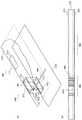
第2の実施形態について説明する。本実施形態では、無線通信装置として無線ルーターを適用する。本実施形態に係る無線ルーターを部屋内に設置した時の状態を図2に示す。本実施形態に係る無線ルーター100は、通常、内部に配置されたプリント基板200が部屋の床面と直交する方向に設置される。そして、本実施形態に係る無線ルーター100を部屋内に設置した時、プリント基板200の右上領域に無線IC300が、その近傍にSRR(Sprit Ring Resonator:スプリットリング共振器)アンテナ400が、SRRアンテナ400の下方にダミーSRR500が配置される。以下、床面と平行な面をXY面、無線ルーター100の背面と平行な面をYZ面とする。(Second Embodiment)
A second embodiment will be described. In the present embodiment, a wireless router is applied as the wireless communication device. FIG. 2 shows a state when the wireless router according to the present embodiment is installed in the room. In the
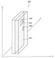
図2のように無線ルーター100を部屋内の床面(XY面)に設置した時、無線ルーター100とスマートフォンやタブレット等の対抗機とはXY方向に対向する。無線ルーター100は対抗機との間で電波を送受信することから、XY方向のアンテナ利得が最も重要となる。 When the
プリント基板200は、無線ルーター100を部屋内に設置した時に床面と直交する。プリント基板200には、無線IC300、SRRアンテナ400およびダミーSRR500の他、図示されない多数の電気部品が実装されている。プリント基板200の正面図を図3(a)に、A−A線で切断した時の断面図を図3(b)に示す。プリント基板200は、図3(b)に示すように、誘電体230の前面に第1導体層210を、後面に第2導体層220を配置することによって構成される。ここで、本実施形態に係るプリント基板200のZ方向の長さは、無線IC300が扱う電波の波長λと略同じ長さに形成されている。 The printed
無線IC300は、プリント基板200の前面に配置され、SRRアンテナ400を介して、図示しないスマートフォンやタブレット等の対抗機との間で電波を送受信する。本実施形態において、無線IC300は、他の電気部品とのトレードオフの結果、プリント基板200の上端から略λ/4下方位置に配置されている。 The
SRRアンテナ400は、プリント基板200の端部に配置され、対抗機から受信した電波を無線IC300へ送信し、無線IC300から受信した電波を対抗機へ送信する。SRRアンテナ400は、電波の通過ロスを最小限にするために、無線IC300の入出力端子の極近に配置される。無線IC300がプリント基板200の上端から略λ/4下方位置に配置されていることから、本実施形態のSRRアンテナ400はプリント基板200の上端からλ/4下方位置の端部に配置される。 The
ダミーSRR500は、SRRアンテナ400からλ/4下方、すなわち、プリント基板200のZ方向の中心位置(λ/2の高さ)に配置される。ダミーSRR500は、SRRアンテナ400からλ/4下方位置において、SRRアンテナ400から発せられる高周波電流を吸収する。
SRRアンテナ400およびダミーSRR500について詳細に説明する。SRRアンテナ400およびダミーSRR500の分解斜視図を図4(a)に、断面図を図4(b)に、SRRアンテナ400およびダミーSRR500の機能構成図を図5(a)、(b)にそれぞれ示す。 The
SRRアンテナ400は、図4に示すように、背景技術で説明した図13のSRRアンテナと同様に構成され、第1スプリットリング部401、第2スプリットリング部402、複数の導電ビア403および給電線404によって構成される。 As shown in FIG. 4, the
第1スプリットリング部401は、第1導体層210の無線IC300近傍の端部領域に第1開口211を形成し、第1開口211と第1導体層210の端部との間に形成された帯状領域を分断する第1切欠212をさらに形成することによって、スプリットリング型に形成される。 The first
第2スプリットリング部402は、同様に、第2導体層220の第1開口211と対向する位置に第2開口221を形成し、さらに、第1切欠212と対向する位置に第2切欠222を形成することによって、スプリットリング型に形成される。 Similarly, the second
導電ビア403は、開口211、212の周囲に複数配置される。導電ビア403は、例えば、第1導体層210、誘電体230および第2導体層220をドリルによって貫通させ、内部をめっきすることによって形成される。 A plurality of
給電線404は、誘電体230の内部に配置された長尺の導電層である。給電線404の一端は導電ビア403に接続され、他端はプリント基板200の反対側の端部において図示しないRF(Radio Frequency)回路に接続されている。 The
本実施形態では、第1スプリットリング部401、第2スプリットリング部402および給電線404を銅箔によって形成した。なお、第1スプリットリング部401、第2スプリットリング部402および給電線404は導電性であれば他の材料によって形成されても良い。 In the present embodiment, the first
上記のように構成されたSRRアンテナ400は、第1切欠212および第2切欠222によって生じるキャパシタンスと、第1開口211および第2開口221の周囲をリング状に流れる電流によって生じるインダクタンスとにより、LC直列共振回路を構成する。 The
すなわち、図5(a)において点線で示した左側領域によって、スプリットリング共振器が構成される。スプリットリング共振器の給電点に給電線404を介してRF回路から高周波信号が給電されることにより、SRRアンテナ400が共振周波数付近においてアンテナとして機能する。なお、第1開口211および第2開口221の大きさを大きくする、または、第1切欠212および第2切欠222の幅を狭くすることによって、共振周波数を低周波化できる。 That is, a split ring resonator is constituted by the left region indicated by the dotted line in FIG. When the high frequency signal is fed from the RF circuit to the feed point of the split ring resonator via the
また、図5(a)において一点鎖線で示した右側領域によって、インピーダンス整合用ループが構成される。インピーダンス整合用ループにより、無線IC300の入出力端子とSRRアンテナ400とのインピーダンス整合を行う。 In addition, an impedance matching loop is configured by the right side region indicated by the alternate long and short dash line in FIG. Impedance matching between the input / output terminals of the
ダミーSRR500は、図4(a)に示すように、第1導体層210の端部領域に第3開口213を形成し、第3開口213と第1導体層210の端部との間に形成された帯状領域を分断する第3切欠214をさらに形成することによって、スプリットリング型に形成される。そして、図5(b)に示すように、ダミーSRR500は、第3切欠214に生じるキャパシタンスと、第3開口213の周囲をリング状に流れる電流によって生じるインダクタンスとから、LC直列共振回路を構成する。ダミーSRR500はスプリットリング共振器として機能し、所望の周波数の電流を吸収する。 As shown in FIG. 4A, the
上記のように構成されたSRRアンテナ400およびダミーSRR500を備えた無線ルーター100をWiFi(ワイファイ、Wireless Fidelity、周波数:2.4GHz、λ=125mm)に適用した場合のアンテナ特性について検討する。以下、プリント基板200のZ方向の長さをWiFiで使用される電波の波長λと同じ125mmに形成し、プリント基板200の右側側辺の上端からλ/4高さの位置にSRRアンテナ400を、λ/2高さの位置(中央位置)にダミーSRR500を配置した場合について説明する。 The antenna characteristics when the
なお、比較として、ダミーSRRを配置していない、背景技術で説明した図11の無線ルーター900をWiFiに適用した場合のアンテナ特性も合わせて示す。 For comparison, an antenna characteristic when the
ダミーSRRを配置していない無線ルーター900をWiFiに適用した場合のアンテナ利得を図6(a)に、ダミーSRR500を配置した無線ルーター100をWiFiに適用した場合のアンテナ利得を図6(b)に示す。なお、アンテナ利得の理想放射パターンを図6(a)、(b)にそれぞれ点線で示す。 6A shows the antenna gain when the
図6(a)に示すように、ダミーSRRが配置されていない無線ルーター900のアンテナ利得はXYの全方向において低く、特に、SRRアンテナが配置されていない側の利得が顕著に低い。一方、図6(b)に示すように、本実施形態に係る無線ルーター100は、SRRアンテナ400のλ/4下方にダミーSRR500が配置されることによって、アンテナ利得が理想放射パターンとほぼ一致する。 As shown in FIG. 6A, the antenna gain of the
これは、SRRアンテナ400のλ/4下方にダミーSRR500を配置することによってSRRアンテナ400から発せられる互いに向きが異なる高周波電流がダミーSRR500によって吸収されるためである。ここで、高周波電流とはまさに電波を放射するための高周波の交流電流であり、WiFi(周波数:2.4GHz)の場合は1秒間に2億4千回振幅する交流電流である。 This is because the
ダミーSRRを配置しない無線ルーター900をWiFiに適用した場合の高周波電流の状態を図7(a)に、本実施形態に係る無線ルーター100をWiFiに適用した場合の高周波電流の状態を図7(b)に示す。 FIG. 7A shows the state of the high-frequency current when the
図7(a)に示すように、ダミーSRRを配置しない無線ルーター900の場合、SRRアンテナから発せられた上端部から下方へ流れる高周波電流αと、下端部から上方へ流れる高周波電流βとが、互いに打ち消し合う。この場合、スプリットリング共振器としての機能が低下し、XY方向のアンテナ利得が低下する。 As shown in FIG. 7A, in the case of the
一方、図7(b)に示すように、SRRアンテナ400からλ/4下方位置にダミーSRR500を配置する場合、SRRアンテナ400から発せられた互いに向きが異なる高周波電流がダミーSRR500によって吸収され、互いに打ち消し合うことが低減される。これにより、XY方向のアンテナ利得が低下することが抑制される。 On the other hand, as shown in FIG. 7B, when the
なお、プリント基板200の端部の中央高さにSRRアンテナ400を配置できる場合は、高周波電流αと高周波電流βとが互いに打消し合うことがなく、アンテナ利得の低下は発生しない。 When the
上記のように、本実施形態に係る無線ルーター100は、SRRアンテナ400をプリント基板200の端部の中央高さに配置できない場合に、SRRアンテナ400からλ/4下方位置にダミーSRR500を配置した。これにより、SRRアンテナ400から発せられる互いに向きが異なる2つの高周波電流がダミーSRR500によって吸収され、高周波電流同士が打消し合うことが低減される。従って、他部品とのトレードオフの結果、プリント基板200の中央高さにSRRアンテナ400を配置できない場合においても、床面と平行な方向のアンテナ利得を良好に維持することができる。 As described above, in the
なお、本実施形態では、プリント基板200のZ方向の長さを、無線IC300が扱う電波の波長λと略同じ長さに形成したが、λよりも長く形成することもできる。この場合、SRRアンテナ400の上下にλ/4の間隔でダミーSRR500を配置すれば良い。λ/4の間隔でダミーSRR500を配置することにより、ダミーSRR500において不要な高周波電流が吸収され、XY方向のアンテナ利得が良好に維持される。 In the present embodiment, the length in the Z direction of the printed
(第3の実施形態)
第3の実施形態について説明する。本実施形態に係る無線ルーターは、MIMO(Multiple-input and Multiple-output)技術に対応する。MIMO技術とは、複数のアンテナを組み合わせることによって広い通信帯域に対応する無線通信技術であり、WiFiやLTE(Long Term Evolution)等の通信方式に適用される。本実施形態に係る無線ルーター100Bは、第2の実施形態で説明した図2の無線ルーター100と同様に構成されると共に、MIMO技術に対応するために2つのSRRアンテナが内部に配置されている。(Third embodiment)
A third embodiment will be described. The wireless router according to the present embodiment corresponds to MIMO (Multiple-input and Multiple-output) technology. The MIMO technology is a wireless communication technology that supports a wide communication band by combining a plurality of antennas, and is applied to communication methods such as WiFi and LTE (Long Term Evolution). The wireless router 100B according to the present embodiment is configured in the same manner as the
本実施形態に係る無線ルーター100B内に配置されているプリント基板の正面図を図8に示す。図8に示すように、プリント基板200BはZ方向の長さがλに形成され、プリント基板200Bの上端からλ/4下方位置に無線IC310Bが、プリント基板200Bの下端からλ/4上方位置に無線IC320Bが配置されている。 FIG. 8 shows a front view of a printed circuit board arranged in the wireless router 100B according to the present embodiment. As shown in FIG. 8, the printed
そして、プリント基板200Bの無線IC310Bと同じ高さの端部領域にSRRアンテナ410Bが、プリント基板200Bの無線IC320Bと同じ高さの端部領域にSRRアンテナ420Bが配置されている。また、プリント基板200BのZ方向中央(λ/2)の端部領域にダミーSRR500Bが配置されている。 The
SRRアンテナ410BおよびSRRアンテナ420Bは、第2の実施形態で説明した図4のSRRアンテナ400と同様に構成され、ダミーSRR500Bは、第2の実施形態で説明した図4のダミーSRR500と同様に構成される。つまり、SRRアンテナ410BおよびSRRアンテナ420Bはスプリットリング共振器を構成し、給電点に高周波信号が給電されることによってアンテナとして機能する。また、ダミーSRR500Bは、スプリットリング共振器を構成し、SRRアンテナ410BおよびSRRアンテナ420Bから発せられた高周波電流を吸収する。 The
2つのSRRアンテナを配置した無線ルーターにおいて、ダミーSRRを配置しない場合の高周波電流の状態を図9(a)に、ダミーSRR500Bを配置した時の高周波電流の状態を図9(b)に示す。また、2つのSRRアンテナを配置した無線ルーターをWiFiに適用した場合において、ダミーSRRを配置しない場合のアイソレーショングラフを図10(a)に、ダミーSRR500Bを配置した時のアイソレーショングラフを図10(b)に示す。ここで、WiFiでは周波数:2.4GHzの電波が使用される。 FIG. 9A shows the state of the high-frequency current when the dummy SRR is not arranged in the wireless router having two SRR antennas, and FIG. 9B shows the state of the high-frequency current when the
アイソレーションとは、複数のアンテナ同士の干渉を示す度合いである。アイソレーションが小さい状態とは、複数のアンテナ同士の干渉が大きく、互いのアンテナ特性に悪影響を及ぼしている状態である。図10において、X軸は周波数(MHz)、Y軸はアイソレーション(dB)である。なお、図10のY軸は、下に向かうほどアイソレーションが改善されるようにした。 Isolation is a degree indicating interference between a plurality of antennas. The state in which the isolation is small is a state in which interference between a plurality of antennas is large and adversely affects each other's antenna characteristics. In FIG. 10, the X axis is frequency (MHz) and the Y axis is isolation (dB). It should be noted that the Y-axis in FIG. 10 is improved in isolation toward the bottom.
図9(a)に示すように、ダミーSRRを配置しない場合、SRRアンテナ410Bから発せられた上端部から下方へ流れる高周波電流α1および下端部から上方へ流れる高周波電流β1、SRRアンテナ420Bから発せられた上端部から下方へ流れる高周波電流α2および下端部から上方へ流れる高周波電流β2が、互いに干渉して打ち消し合う。この場合、図10(a)に示すように、ターゲットである2400〜2500(MHz)において十分なアイソレーションが得られない。 As shown in FIG. 9A, when the dummy SRR is not arranged, the high-frequency current α1 flowing downward from the upper end portion emitted from the
一方、図9(b)に示すように、ダミーSRR500Bを配置することにより、例えば、SRRアンテナ410Bから発せられる下端部から上方へ流れる高周波電流β1と、SRRアンテナ420Bから発せられる上端部から下方へ流れる高周波電流α2とが、ダミーSRR500Bによって吸収され、干渉が小さくなる。その結果、図10(b)に示すように、ターゲットである2400〜2500(MHz)において、アイソレーションが数dB改善される。 On the other hand, as shown in FIG. 9B, by arranging the
なお、本実施形態においては、プリント基板200BのZ方向の長さをλに形成し、Z方向にλ/4の間隔で、SRRアンテナ410B、ダミーSRR500BおよびSRRアンテナ420Bをこの順に配置したが、これに限定されない。例えば、プリント基板200BのZ方向の長さがλより大きい場合は、λ/4の間隔でSRRアンテナとダミーSRRとを交互に配置することにより、アイソレーションの悪化を抑制することができる。 In the present embodiment, the length of the printed
(第3の実施形態の変形例)
第3の実施形態においては、アンテナとしてSRRアンテナ410B、420Bを適用したが、これに限定されない。例えば、アンテナとして逆L型アンテナを適用することもできる。無線ルーター100C内に2つの逆L型アンテナを配置した時のプリント基板の正面図を図11に示す。(Modification of the third embodiment)
In the third embodiment, the
図11に示すように、プリント基板200CはZ方向の長さがλに形成され、プリント基板200Cの上端からλ/4下方位置に無線IC310Cが、プリント基板200Cの下端からλ/4上方位置に無線IC320Cが配置されている。そして、プリント基板200Cの無線IC310Cと同じ高さの端部領域に逆L型アンテナ610Cが、プリント基板200Cの無線IC320Cと同じ高さの端部領域に逆L型アンテナ620Cが配置されている。また、プリント基板200CのZ方向中央(λ/2)の端部領域にダミーSRR500Cが配置されている。 As shown in FIG. 11, the printed circuit board 200C is formed with a length of λ in the Z direction, and the
そして、逆L型アンテナ610C、620Cを適用した場合において、ダミーSRRを配置しない場合のアイソレーショングラフを図12(a)に、ダミーSRR500Cを配置した時のアイソレーショングラフを図12(b)に示す。 When the inverted L antennas 610C and 620C are applied, the isolation graph when the dummy SRR is not arranged is shown in FIG. 12A, and the isolation graph when the
逆L型アンテナを適用した場合においても、逆L型アンテナ610C、620Cからそれぞれλ/4だけ離れた位置にダミーSRR500Cを配置することにより、例えば、逆L型アンテナ610Cから発せられる下端部から上方へ流れる高周波電流と、逆L型アンテナ620Cから発せられる上端部から下方へ流れる高周波電流とが、ダミーSRR500Cによって吸収され、干渉が小さくなる。その結果、図12(b)に示すように、ターゲットである2400〜2500(MHz)において、アイソレーションが数dB改善される。 Even when the inverted L-type antenna is applied, the
本願発明は上記実施形態に限定されるものではなく、この発明の要旨を逸脱しない範囲の設計の変更等があってもこの発明に含まれる。 The present invention is not limited to the above-described embodiment, and design changes and the like within a range not departing from the gist of the present invention are included in the present invention.
10、10B アンテナ
20、20B プリント配線基板
30、31B、32B アンテナ回路
40、40B 直列共振回路
100、100B、100C 無線ルーター
200、200B、200C プリント基板
210、220 導体層
211、213、221 開口
212、214、222 切欠
230 誘電体
300、310B、320B 無線IC
400、410B、420B SRRアンテナ
401 第1スプリットリング部
402 第2スプリットリング部
403 導電ビア
404 給電線
500、500B、500C ダミーSRR
610C、620C 逆L型アンテナ
900 アンテナ
910 多層化プリント基板
920 誘電体層
930、940 導体層
931、941 開口
932、942 切欠
950 SRRアンテナ
951、952 スプリットリング部
953 導電ビア
954 給電線10,
400, 410B,
610C, 620C Reverse
Claims (9)
Translated fromJapanese前記導体板の面内の第1の開口が前記第1の端部と第1の空隙で接続され前記第1の開口と第2の端部との最短距離が第1の距離であるスプリットリングアンテナ素子と、
前記導体板の面内の第2の開口が前記第1の端部と第2の空隙で接続され前記第2の開口と前記第2の端部との最短距離が第2の距離であるスプリットリング共振器とを備えることを特徴とするアンテナ。A conductor plate having a linear first end and a linear second end orthogonal to each other;
A split ring in which a first opening in a plane of the conductor plate is connected to the first end by a first gap, and a shortest distance between the first opening and the second end is a first distance. An antenna element;
A split in which a second opening in the plane of the conductor plate is connected to the first end by a second gap, and a shortest distance between the second opening and the second end is a second distance. An antenna comprising aring resonator .
前記第1の距離は前記スプリットリングアンテナ素子の動作波長に対して略1/4であり、前記第2の距離は、前記スプリットリングアンテナ素子の動作波長に対して略1/2であることを特徴とする請求項1に記載のアンテナ。The length of the first end is substantially equal to the operating wavelength of the split ring antenna element,
The first distance is approximately ¼ of the operating wavelength of the split ring antenna element, and the second distance is approximately ½ of the operating wavelength of the split ring antenna element. The antenna accordingto claim 1 .
前記導体板の面内の第3の開口が前記第1の端部と第3の空隙で接続され前記第3の開口と前記第3の端部との最短距離が第3の距離であるスプリットリングアンテナ素子を更に備えることを特徴とする請求項1に記載のアンテナ。The conductor plate further includes the third end portion in a straight line parallel to the second end portion,
A split in which a third opening in the plane of the conductor plate is connected to the first end by a third gap, and the shortest distance between the third opening and the third end is a third distance. The antenna according to claim 1, further comprising a ring antenna element .
前記第1の距離および前記第3の距離は前記スプリットリングアンテナ素子の動作波長に対して略1/4であり、前記第2の距離は、前記スプリットリングアンテナ素子の動作波長に対して略1/2であることを特徴とする請求項3に記載のアンテナ。The length of the first end is substantially equal to the operating wavelength of the split ring antenna element,
The first distance and the third distance are approximately 1/4 with respect to the operating wavelength of the split ring antenna element, and the second distance is approximately 1 with respect to the operating wavelength of the split ring antenna element. The antenna accordingto claim 3, which is / 2 .
第2の端部との最短距離が第1の距離であり前記導体板上に搭載される部品の前記導体板の板厚方向の高さの間隙をもち前記第2の端部と平行な第1の導体部と、前記第1の導体部の先端に接続され前記導体板の延伸に対して前記間隙を有し前記第1の端部と平行な第2の導体部を有する逆L型アンテナ素子と、 The shortest distance to the second end is the first distance, and a component mounted on the conductor plate has a gap in the thickness direction of the conductor plate and has a height parallel to the second end. An inverted L-shaped antenna having a first conductor portion and a second conductor portion connected to the tip of the first conductor portion and having the gap with respect to the extension of the conductor plate and parallel to the first end portion Elements,
前記導体板の面内の開口が前記第1の端部と第2の空隙で接続され前記開口と前記第2の端部との最短距離が第2の距離であるスプリットリング共振器とを備えることを特徴とするアンテナ。 An opening in a plane of the conductor plate is connected to the first end portion by a second gap, and a split ring resonator having a shortest distance between the opening and the second end portion is a second distance. An antenna characterized by that.
前記第1の距離は、前記逆L型アンテナ素子の動作波長に対して略1/4であり、前記第2の距離は、前記逆L型アンテナ素子の動作波長に対して略1/2であることを特徴とする請求項5に記載のアンテナ。The length of the first end is substantially equal to the operating wavelength of the inverted L antenna element,
The first distance is approximately 1/4 with respect to the operating wavelength of the inverted L-type antenna element, and the second distance is approximately 1/2 with respect to the operating wavelength of the inverted L-type antenna element. The antenna accordingto claim 5, wherein the antennais provided.
第2の端部との最短距離が第3の距離であり前記導体板上に搭載される部品の前記導体板の板厚方向の高さの間隙をもち前記第2の端部と平行な第1の導体部と、前記第1の導体部の先端に接続され前記導体板の延伸に対して前記間隙を有し前記第1の端部と平行な第2の導体部を有する逆L型アンテナ素子を更に備えることを特徴とする請求項5に記載のアンテナ。The conductor plate further includes the third end portion in a straight line parallel to the second end portion,
The shortest distance from the second end is the third distance, and a part mounted on the conductor plate has a height gap in the thickness direction of the conductor plate and is parallel to the second end. An inverted L-shaped antenna having a first conductor portion and a second conductor portion connected to the tip of the first conductor portion and having the gap with respect to the extension of the conductor plate and parallel to the first end portion The antenna accordingto claim 5, further comprising an element .
前記第1の距離および前記第3の距離は前記逆L型アンテナ素子の動作波長に対して略1/4であり、前記第2の距離は、前記逆L型アンテナ素子の動作波長に対して略1/2であることを特徴とする請求項7に記載のアンテナ。The length of the first end is substantially equal to the operating wavelength of the inverted L antenna element,
The first distance and the third distance are approximately 1/4 with respect to the operating wavelength of the inverted L-type antenna element, and the second distance is relative to the operating wavelength of the inverted L-type antenna element. The antenna accordingto claim 7, wherein the antennais approximately ½ .
前記アンテナに接続される無線回路とを備えることを特徴とする無線通信装置。An antenna according to any one of claims 1 to 8,
A wireless communication devicecomprising: a wireless circuit connected to the antenna .
Priority Applications (4)
| Application Number | Priority Date | Filing Date | Title |
|---|---|---|---|
| JP2013175562AJP5947263B2 (en) | 2013-08-27 | 2013-08-27 | Antenna and wireless communication device |
| CN201480047999.3ACN106063031B (en) | 2013-08-27 | 2014-07-23 | Antenna and wireless communication device |
| PCT/JP2014/003870WO2015029322A1 (en) | 2013-08-27 | 2014-07-23 | Antenna and wireless communication apparatus |
| US14/910,348US10374285B2 (en) | 2013-08-27 | 2014-07-23 | Antenna and wireless communication apparatus |
Applications Claiming Priority (1)
| Application Number | Priority Date | Filing Date | Title |
|---|---|---|---|
| JP2013175562AJP5947263B2 (en) | 2013-08-27 | 2013-08-27 | Antenna and wireless communication device |
Publications (2)
| Publication Number | Publication Date |
|---|---|
| JP2015046681A JP2015046681A (en) | 2015-03-12 |
| JP5947263B2true JP5947263B2 (en) | 2016-07-06 |
Family
ID=52585922
Family Applications (1)
| Application Number | Title | Priority Date | Filing Date |
|---|---|---|---|
| JP2013175562AActiveJP5947263B2 (en) | 2013-08-27 | 2013-08-27 | Antenna and wireless communication device |
Country Status (4)
| Country | Link |
|---|---|
| US (1) | US10374285B2 (en) |
| JP (1) | JP5947263B2 (en) |
| CN (1) | CN106063031B (en) |
| WO (1) | WO2015029322A1 (en) |
Families Citing this family (9)
| Publication number | Priority date | Publication date | Assignee | Title |
|---|---|---|---|---|
| JP6606871B2 (en)* | 2015-06-04 | 2019-11-20 | 日本電気株式会社 | Antenna and wireless communication device |
| JP2017130770A (en)* | 2016-01-20 | 2017-07-27 | 株式会社村田製作所 | Antenna device |
| CN106785476B (en)* | 2017-02-28 | 2019-12-27 | 南京理工大学 | Metamaterial wave absorber |
| JP6658974B1 (en) | 2018-07-24 | 2020-03-04 | 株式会社村田製作所 | RFID tag reading antenna |
| EP3826110A4 (en)* | 2018-09-12 | 2021-08-25 | Japan Aviation Electronics Industry, Limited | ANTENNA AND COMMUNICATION DEVICE |
| KR102542096B1 (en)* | 2019-04-17 | 2023-06-13 | 니혼 고꾸 덴시 고교 가부시끼가이샤 | Split-ring resonators and communication devices |
| EP3988022A4 (en)* | 2019-06-21 | 2023-07-26 | UNIST (Ulsan National Institute of Science and Technology) | RESONATOR ASSEMBLY FOR BIOMETRIC AND BIOSENSOR DETECTION USING ELECTROMAGNETIC WAVES |
| US11251522B2 (en) | 2019-08-15 | 2022-02-15 | Ademco Inc. | Cancelation circuit for radio frequency antenna systems |
| JP7315235B2 (en)* | 2020-10-30 | 2023-07-26 | Necプラットフォームズ株式会社 | antenna device |
Family Cites Families (57)
| Publication number | Priority date | Publication date | Assignee | Title |
|---|---|---|---|---|
| GB0102768D0 (en)* | 2001-02-02 | 2001-03-21 | Koninkl Philips Electronics Nv | Wireless terminal |
| US6985114B2 (en)* | 2003-06-09 | 2006-01-10 | Houkou Electric Co., Ltd. | Multi-frequency antenna and constituting method thereof |
| US7009565B2 (en)* | 2004-07-30 | 2006-03-07 | Lucent Technologies Inc. | Miniaturized antennas based on negative permittivity materials |
| JP2007013643A (en)* | 2005-06-30 | 2007-01-18 | Lenovo Singapore Pte Ltd | Integrally formed flat-plate multi-element antenna and electronic apparatus |
| KR100699472B1 (en)* | 2005-09-27 | 2007-03-26 | 삼성전자주식회사 | Flat Panel Array Antenna with Isolation Element |
| US7492329B2 (en)* | 2006-10-12 | 2009-02-17 | Hewlett-Packard Development Company, L.P. | Composite material with chirped resonant cells |
| JP5294443B2 (en)* | 2007-06-21 | 2013-09-18 | 三星電子株式会社 | Antenna device and wireless communication terminal |
| WO2010008785A2 (en)* | 2008-06-24 | 2010-01-21 | Federal-Mogul Corporation | Wrist pin, connecting rod, piston and piston assembly therewith and methods of constructing and assembling the same |
| JP5304220B2 (en)* | 2008-12-24 | 2013-10-02 | 富士通株式会社 | Antenna device, printed circuit board including antenna device, and wireless communication device including antenna device |
| US8085202B2 (en)* | 2009-03-17 | 2011-12-27 | Research In Motion Limited | Wideband, high isolation two port antenna array for multiple input, multiple output handheld devices |
| US8552913B2 (en)* | 2009-03-17 | 2013-10-08 | Blackberry Limited | High isolation multiple port antenna array handheld mobile communication devices |
| TWI420739B (en)* | 2009-05-21 | 2013-12-21 | Ind Tech Res Inst | Radiation pattern insulator and antenna system thereof and communication device using the antenna system |
| TWI420743B (en)* | 2009-11-13 | 2013-12-21 | Ralink Technology Corp | Dual frequency printed circuit antenna for electronic devices |
| JP5532847B2 (en)* | 2009-11-20 | 2014-06-25 | 船井電機株式会社 | Multi-antenna device and portable device |
| JP5482171B2 (en)* | 2009-12-11 | 2014-04-23 | 富士通株式会社 | ANTENNA DEVICE AND WIRELESS TERMINAL DEVICE |
| KR101241388B1 (en)* | 2009-12-18 | 2013-03-12 | 한국전자통신연구원 | Multi Input Multi Output antenna for improving the isolation characteristic |
| FI124066B (en)* | 2010-06-01 | 2014-02-28 | Marisense Oy | Arrangements for reducing interference in an electronic shelf label |
| TWI455404B (en)* | 2010-11-02 | 2014-10-01 | Ind Tech Res Inst | Structure for adjusting em wave penetration response and antenna structure for adjusting em wave radiation characteristic |
| US8890763B2 (en)* | 2011-02-21 | 2014-11-18 | Funai Electric Co., Ltd. | Multiantenna unit and communication apparatus |
| JP5673270B2 (en)* | 2011-03-22 | 2015-02-18 | 船井電機株式会社 | Multi-antenna device and communication device |
| US8816921B2 (en)* | 2011-04-27 | 2014-08-26 | Blackberry Limited | Multiple antenna assembly utilizing electro band gap isolation structures |
| CN102760949A (en)* | 2011-04-27 | 2012-10-31 | 鸿富锦精密工业(深圳)有限公司 | Multiple-input-and-output antenna |
| DE102011002320B3 (en)* | 2011-04-28 | 2012-06-21 | Knauf Gips Kg | Method and device for generating electricity from hydrogen sulfide-containing exhaust gases |
| US9444129B2 (en)* | 2011-05-13 | 2016-09-13 | Funai Electric Co., Ltd. | Multi-band compatible multi-antenna device and communication equipment |
| JP5791961B2 (en)* | 2011-05-13 | 2015-10-07 | 船井電機株式会社 | Multi-antenna device and communication device |
| US9236653B2 (en)* | 2011-05-17 | 2016-01-12 | Kuang-Chi Innovative Technology Ltd. | Antenna device |
| US9306276B2 (en)* | 2011-07-13 | 2016-04-05 | Qualcomm Incorporated | Wideband antenna system with multiple antennas and at least one parasitic element |
| JP5885416B2 (en)* | 2011-07-14 | 2016-03-15 | キヤノン株式会社 | IMAGING DEVICE AND IMAGING DEVICE CONTROL METHOD |
| CN103748741B (en)* | 2011-08-24 | 2016-05-11 | 日本电气株式会社 | Antennas and Electronics |
| JP5162012B1 (en)* | 2011-08-31 | 2013-03-13 | 株式会社東芝 | ANTENNA DEVICE AND ELECTRONIC DEVICE HAVING THE ANTENNA DEVICE |
| TWI495197B (en)* | 2011-10-11 | 2015-08-01 | Univ Southern Taiwan | Monopole slot antenna of multiple-input and multiple-output with good isolation degree |
| JP5076019B1 (en)* | 2011-10-19 | 2012-11-21 | 株式会社東芝 | ANTENNA DEVICE AND ELECTRONIC DEVICE HAVING THE ANTENNA DEVICE |
| TWI493789B (en)* | 2011-10-28 | 2015-07-21 | Hon Hai Prec Ind Co Ltd | An antenna |
| JP5708475B2 (en)* | 2011-12-26 | 2015-04-30 | 船井電機株式会社 | Multi-antenna device and communication device |
| JPWO2013145623A1 (en)* | 2012-03-28 | 2015-12-10 | 日本電気株式会社 | ANTENNA DEVICE AND PORTABLE RADIO DEVICE HAVING THE SAME |
| TWI511378B (en)* | 2012-04-03 | 2015-12-01 | Ind Tech Res Inst | Multi-band multi-antenna system and communiction device thereof |
| TWI513104B (en)* | 2012-08-28 | 2015-12-11 | Compal Electronics Inc | Electronic device |
| US8922448B2 (en)* | 2012-09-26 | 2014-12-30 | Mediatek Singapore Pte. Ltd. | Communication device and antennas with high isolation characteristics |
| CN104781986B (en)* | 2012-11-12 | 2019-07-12 | 日本电气株式会社 | Antenna and wireless telecom equipment |
| TWI539672B (en)* | 2012-11-16 | 2016-06-21 | 宏碁股份有限公司 | Communication device |
| JP6102211B2 (en)* | 2012-11-20 | 2017-03-29 | 船井電機株式会社 | Multi-antenna device and communication device |
| JP2014116883A (en)* | 2012-12-12 | 2014-06-26 | Sony Corp | Antenna device and communication device |
| CN203339302U (en)* | 2013-01-28 | 2013-12-11 | 中兴通讯股份有限公司 | Antenna system |
| WO2014129147A1 (en)* | 2013-02-20 | 2014-08-28 | Necアクセステクニカ株式会社 | Antenna device and method for designing same |
| JP5725573B2 (en)* | 2013-02-26 | 2015-05-27 | Necプラットフォームズ株式会社 | Antenna and electronic device |
| US9960483B2 (en)* | 2013-02-26 | 2018-05-01 | Nec Corporation | Antenna, printed circuit board, and wireless communication device |
| US9019160B2 (en)* | 2013-03-18 | 2015-04-28 | King Fahd University Of Petroleum And Minerals | CSRR-loaded MIMO antenna systems |
| TW201442340A (en)* | 2013-04-18 | 2014-11-01 | Ind Tech Res Inst | Multi-antenna system |
| WO2014192268A1 (en)* | 2013-05-28 | 2014-12-04 | 日本電気株式会社 | Mimo antenna device |
| CN104466401B (en)* | 2013-09-25 | 2019-03-12 | 中兴通讯股份有限公司 | Multi-antenna terminal |
| JP6183249B2 (en)* | 2014-03-13 | 2017-08-23 | 富士通株式会社 | Wireless device |
| US11079339B2 (en)* | 2014-09-24 | 2021-08-03 | Bogazici Universitesi | Biosensor with integrated antenna and measurement method for biosensing applications |
| US10067075B2 (en)* | 2014-09-24 | 2018-09-04 | Bogazici Universitesi | Biosensor with integrated antenna and measurement method for biosensing applications |
| TW201712950A (en)* | 2015-09-23 | 2017-04-01 | 啟碁科技股份有限公司 | Antenna system |
| TW201739105A (en)* | 2016-04-28 | 2017-11-01 | 智易科技股份有限公司 | Dual-band antenna |
| JP6659519B2 (en)* | 2016-11-02 | 2020-03-04 | 株式会社東芝 | Antenna device |
| TWI618296B (en)* | 2017-03-15 | 2018-03-11 | 智易科技股份有限公司 | Antenna structure |
- 2013
- 2013-08-27JPJP2013175562Apatent/JP5947263B2/enactiveActive
- 2014
- 2014-07-23CNCN201480047999.3Apatent/CN106063031B/enactiveActive
- 2014-07-23WOPCT/JP2014/003870patent/WO2015029322A1/enactiveApplication Filing
- 2014-07-23USUS14/910,348patent/US10374285B2/enactiveActive
Also Published As
| Publication number | Publication date |
|---|---|
| CN106063031A (en) | 2016-10-26 |
| CN106063031B (en) | 2020-03-03 |
| US10374285B2 (en) | 2019-08-06 |
| JP2015046681A (en) | 2015-03-12 |
| WO2015029322A1 (en) | 2015-03-05 |
| US20160190676A1 (en) | 2016-06-30 |
Similar Documents
| Publication | Publication Date | Title |
|---|---|---|
| JP5947263B2 (en) | Antenna and wireless communication device | |
| US11011843B2 (en) | Antenna element, antenna module, and communication apparatus | |
| US10224622B2 (en) | Antennas including dual radiating elements for wireless electronic devices | |
| TWI628846B (en) | Antenna structure and wireless communication device having the same | |
| EP3667817B1 (en) | Antenna device and terminal | |
| CN107534206B (en) | Wireless electronic device | |
| KR102138841B1 (en) | Antenna device | |
| JP6763372B2 (en) | Multi-band antenna and wireless communication device | |
| US10476132B2 (en) | Antenna, antenna array, and radio communication apparatus | |
| WO2006098089A1 (en) | Antenna assembly and radio communication apparatus employing same | |
| JP2015033049A (en) | Antenna device and radio communication equipment employing the same | |
| JP6950084B2 (en) | Patch antenna for millimeter wave communication | |
| JP2017195589A (en) | Antenna and antenna module including the antenna | |
| JP6138839B2 (en) | Antenna structure | |
| KR101670173B1 (en) | Antenna Using Metal Case for Wireless Headset | |
| KR100970016B1 (en) | Built-in Antenna with Stacked Structure | |
| CN210379412U (en) | Antenna, antenna assembly and electronic equipment | |
| JP2018152694A (en) | ANTENNA DEVICE AND ELECTRONIC DEVICE HAVING ANTENNA DEVICE | |
| JP4661816B2 (en) | Antenna and wireless communication device | |
| US20240154316A1 (en) | Antenna | |
| KR101056347B1 (en) | Chip antenna | |
| JP2025025672A (en) | Composite patch antenna device | |
| JP2020098959A (en) | Antenna module and communication device mounting the same | |
| JP2014171087A (en) | Broadband antenna |
Legal Events
| Date | Code | Title | Description |
|---|---|---|---|
| A621 | Written request for application examination | Free format text:JAPANESE INTERMEDIATE CODE: A621 Effective date:20141217 | |
| A131 | Notification of reasons for refusal | Free format text:JAPANESE INTERMEDIATE CODE: A131 Effective date:20160223 | |
| A521 | Written amendment | Free format text:JAPANESE INTERMEDIATE CODE: A523 Effective date:20160408 | |
| TRDD | Decision of grant or rejection written | ||
| A01 | Written decision to grant a patent or to grant a registration (utility model) | Free format text:JAPANESE INTERMEDIATE CODE: A01 Effective date:20160510 | |
| A61 | First payment of annual fees (during grant procedure) | Free format text:JAPANESE INTERMEDIATE CODE: A61 Effective date:20160602 | |
| R150 | Certificate of patent or registration of utility model | Ref document number:5947263 Country of ref document:JP Free format text:JAPANESE INTERMEDIATE CODE: R150 |