JP5945886B2 - Manufacturing support method for multilayer substrate, manufacturing method for multilayer substrate, failure cause identification method, manufacturing support program for multilayer substrate, and multilayer substrate - Google Patents
Manufacturing support method for multilayer substrate, manufacturing method for multilayer substrate, failure cause identification method, manufacturing support program for multilayer substrate, and multilayer substrateDownload PDFInfo
- Publication number
- JP5945886B2 JP5945886B2JP2012040741AJP2012040741AJP5945886B2JP 5945886 B2JP5945886 B2JP 5945886B2JP 2012040741 AJP2012040741 AJP 2012040741AJP 2012040741 AJP2012040741 AJP 2012040741AJP 5945886 B2JP5945886 B2JP 5945886B2
- Authority
- JP
- Japan
- Prior art keywords
- substrate
- stack
- layer
- manufacturing
- film thickness
- Prior art date
- Legal status (The legal status is an assumption and is not a legal conclusion. Google has not performed a legal analysis and makes no representation as to the accuracy of the status listed.)
- Active
Links
Images


Classifications
- Y—GENERAL TAGGING OF NEW TECHNOLOGICAL DEVELOPMENTS; GENERAL TAGGING OF CROSS-SECTIONAL TECHNOLOGIES SPANNING OVER SEVERAL SECTIONS OF THE IPC; TECHNICAL SUBJECTS COVERED BY FORMER USPC CROSS-REFERENCE ART COLLECTIONS [XRACs] AND DIGESTS
- Y02—TECHNOLOGIES OR APPLICATIONS FOR MITIGATION OR ADAPTATION AGAINST CLIMATE CHANGE
- Y02E—REDUCTION OF GREENHOUSE GAS [GHG] EMISSIONS, RELATED TO ENERGY GENERATION, TRANSMISSION OR DISTRIBUTION
- Y02E10/00—Energy generation through renewable energy sources
- Y02E10/50—Photovoltaic [PV] energy
Landscapes
- Electroluminescent Light Sources (AREA)
- Photovoltaic Devices (AREA)
Description
Translated fromJapanese本発明は、積層基板の製造支援方法、積層基板の製造方法、故障原因特定方法、積層基板の製造支援プログラム及び積層基板に関し、特に、積層基板が太陽電池である場合に適用して有用なものである。 The present invention relates to a laminated substrate manufacturing support method, a laminated substrate manufacturing method, a failure cause identifying method, a laminated substrate manufacturing support program, and a laminated substrate, and particularly useful when applied to a laminated substrate that is a solar cell. It is.
受光面への光の入射を促進し光電変換効率を高めるために、光電変換する発電層及び反射防止膜を設けた太陽電池が知られている(例えば、特許文献1参照)。太陽電池等に用いる反射防止技術には、反射率を算出することで、それを低減するように反射防止膜の多層構造の仕様(膜厚等)を決定するものがある。しかし、このような反射防止技術では、太陽電池の性能上、最も重要な発電能力を直接的に評価していないため、発電層における発電性能の十分な向上ができないことがある。 In order to promote the incidence of light on the light receiving surface and increase the photoelectric conversion efficiency, a solar cell provided with a power generation layer for photoelectric conversion and an antireflection film is known (for example, see Patent Document 1). Among the antireflection techniques used for solar cells and the like, there is one that determines the specifications (film thickness and the like) of the multilayer structure of the antireflection film so as to reduce the reflectance by calculating the reflectance. However, such antireflection technology does not directly evaluate the most important power generation capacity in terms of the performance of the solar cell, and therefore may not be able to sufficiently improve the power generation performance in the power generation layer.
また、太陽電池は、通常、厚さがミリメートルオーダーの基板の上に作成されるが、基板以外の構造(太陽電池及び反射防止膜の各層)はナノメートルオーダーの膜厚を有する薄膜であり、基板に比べて非常に薄い。このため、従来の方法では、基板と基板以外の両者を同時に扱った電磁波の解析が困難であった。 In addition, the solar cell is usually formed on a substrate with a thickness on the order of millimeters, but the structure other than the substrate (each layer of the solar cell and the antireflection film) is a thin film having a thickness on the order of nanometers. Very thin compared to the substrate. For this reason, in the conventional method, it has been difficult to analyze the electromagnetic wave simultaneously handling both the substrate and the substrate other than the substrate.
さらに、従来の反射防止膜の設計法は、太陽電池及び反射防止膜を製造する際の、膜厚・屈折率等に関する誤差(製造誤差)の影響を考慮せずに、設計時の状態において最も性能の良い最適解を探すものであった。製造誤差の無い場合には性能が最適解に比べて若干劣っても、製造誤差に対する性能低下レベルが小さい(ロバストである)準最適解が必要な場合が実際には多いが、従来の手法では、製造誤差を考慮することができなかった。 Furthermore, the conventional design method of antireflection film is the most suitable in the state of design without considering the influence of film thickness, refractive index, etc. (manufacturing error) when manufacturing solar cells and antireflection films. We searched for an optimal solution with good performance. When there is no manufacturing error, even though the performance is slightly inferior to the optimal solution, there are actually many cases where a suboptimal solution with a low level of performance degradation against the manufacturing error is required (robust). The manufacturing error could not be taken into account.
なお、このような問題は、太陽電池にのみ生じるものではなく、光を吸収する特定層(太陽電池における発電層)及び反射防止膜を含む積層基板(太陽電池)において、特定層で吸収される光吸収量(太陽電池における発電量)を直接的に評価する場合においても同様に存在する。 In addition, such a problem does not occur only in the solar cell, but is absorbed in the specific layer in the multilayer substrate (solar cell) including the specific layer that absorbs light (power generation layer in the solar cell) and the antireflection film. The same exists when the light absorption amount (power generation amount in the solar cell) is directly evaluated.
本発明は、上記従来技術に鑑み、光を吸収する光吸収層及び反射防止膜(第1積層及び第2積層)を含む積層基板において光吸収層における光吸収量を直接的に評価し、当該光吸収量が最適又は準最適となるような積層基板の膜厚及び材料を得ることができる積層基板の製造支援方法及び積層基板の製造支援プログラムを提供することを目的とする。 In view of the above prior art, the present invention directly evaluates the amount of light absorption in a light absorption layer in a multilayer substrate including a light absorption layer that absorbs light and an antireflection film (first stack and second stack), and It is an object of the present invention to provide a manufacturing support method for a multilayer substrate and a manufacturing support program for the multilayer substrate, which can obtain the film thickness and material of the multilayer substrate so that the light absorption amount is optimal or semi-optimal.
また、積層基板の製造支援方法により得られた膜厚及び材料を用いて、光吸収量が最適又は準最適となるような積層基板の製造方法を提供することを目的とする。ならびに、積層基板の製造支援方法により得られた膜厚及び材料を用いて、積層基板を製造する過程での故障原因を特定する故障原因特定方法を提供することを目的とする。 It is another object of the present invention to provide a method for manufacturing a laminated substrate in which the amount of light absorption is optimal or sub-optimal using the film thickness and material obtained by the method for supporting the production of a laminated substrate. It is another object of the present invention to provide a failure cause identifying method for identifying a cause of a failure in the process of manufacturing a laminated substrate using the film thickness and material obtained by the method for supporting the production of a laminated substrate.
さらに、光吸収量が最適又は準最適となるような膜厚及び材料からなる積層基板を提供することを目的とする。 It is another object of the present invention to provide a laminated substrate made of a film thickness and a material so that the light absorption amount is optimal or semi-optimal.
上記目的を達成するための本発明の第1の態様は、基板と、複数の材料からなる第1積層及び第2積層と、光を吸収する光吸収層とを備え、前記第1積層は前記基板の一方面に設けられ、前記第2積層は前記基板の他方面に設けられ、前記光吸収層は前記第2積層上に設けられた積層基板の製造支援方法であって、前記第1積層及び前記第2積層に用いる材料、並びに前記材料について光の波長に依存する屈折率及び消衰係数を用いて、前記第1積層側から光が入射した際の前記第1積層及び前記第2積層の反射率及び透過率をマトリクス法により求め、前記基板の膜厚から当該基板の内部透過率を計算し、前記第1積層及び前記第2積層の反射率及び透過率並びに前記内部透過率から、前記第1積層側に入射した光が前記光吸収層に吸収される光吸収量を波長ごとに計算し、該光吸収量を積分して総光吸収量を求め、前記総光吸収量が最大となる前記第1積層及び前記第2積層の材料及び膜厚を求めることを特徴とする積層基板の製造支援方法にある。In order to achieve the above object, afirst aspect of the present invention includes a substrate, a first stack and a second stack made of a plurality of materials, and a light absorbing layer that absorbs light. Provided on one side of the substrate, the second stack is provided on the other side of the substrate, and the light absorption layer is a manufacturing support method for a stacked substrate provided on the second stack, the first stack And the material used for the second stack, and the first stack and the second stack when light is incident from the first stack using the refractive index and extinction coefficient depending on the wavelength of light for the material. The reflectance and transmittance of the substrate is obtained by a matrix method, the internal transmittance of the substrate is calculated from the film thickness of the substrate, and the reflectance and transmittance of the first stack and the second stack, and the internal transmittance, Light incident on the first stack side is absorbed by the light absorption layer. Calculating the light absorption amount for each wavelength, integrating the light absorption amount to obtain the total light absorption amount, and determining the materials and film thicknesses of the first and second stacks that maximize the total light absorption amount. It is in the manufacturing support method of the laminated substrate characterized by calculating | requiring.
かかる第1の態様では、光吸収層における光吸収量を十分に向上することができる積層基板の構成を得ることができる。積層基板の一例として太陽電池を含むものであれば、性能上、最も重要な発電電流量を直接的に評価した上で、発電層における発電電流量を十分に向上することができる積層基板の構成を得ることができる。また、厚さがミリメートルオーダーのガラス基板を含む積層基板について、ガラス基板とそれ以外(第1積層、第2積層及び太陽電池)の両者を同時に扱った光の解析が可能となる。In thefirst aspect, it ispossible to obtain a configuration of the laminated substrate that can sufficiently improve the light absorption amount in thelight absorption layer. If a solar cell is included as an example of a multilayer substrate, the configuration of the multilayer substrate that can sufficiently improve the amount of generated current in the power generation layer after directly evaluating the most important amount of generated current in terms of performance Can be obtained. In addition, for a laminated substrate including a glass substrate havinga thickness of the order of millimeters, it is possible to analyze light in which both the glass substrate and the other substrates (first laminated layer, second laminated layer, and solar cell) are handled simultaneously.
本発明の第2の態様は、第1の態様に記載する積層基板の製造支援方法において、前記総光吸収量が最大となる前記第1積層及び前記第2積層の膜厚を求める方法は、前記第1積層及び前記第2積層の各膜厚に初期値として任意の数値を与え、準ニュートン法を用いて前記第1積層及び前記第2積層の膜厚の最適値を求め、当該最適値を求める工程を複数回実行することで、複数の最適値からなる準最適値リストを求めることを特徴とする積層基板の製造支援方法にある。According to asecond aspect of the present invention, in the laminated substrate manufacturing support method described in thefirst aspect, the method of obtaining the film thicknesses of the first and second layers that maximize the total light absorption amount is as follows. Arbitrary numerical values are given as initial values to the respective film thicknesses of the first stack and the second stack, the optimum values of the film thicknesses of the first stack and the second stack are obtained using a quasi-Newton method, The multilayer substrate manufacturing support method is characterized in that a sub-optimal value list including a plurality of optimum values is obtained by executing the step of obtaining a plurality of times.
かかる第2の態様では、複数のランダムな初期値から複数の最適値からなる準最適値リストを求めることができる。In thesecond aspect, a sub-optimal value list including a plurality of optimum values can be obtained from a plurality of random initial values.
本発明の第3の態様は、第1又は第2の態様に記載する積層基板の製造支援方法において、前記第1積層又は前記第2積層について得られた膜厚の最適値と、当該膜厚に対応する総光吸収量との対応を表示すると共に、当該膜厚を一定値で変動させたときの総光吸収量の変動を表示することを特徴とする積層基板の製造支援方法にある。According to athird aspect of the present invention, in the laminated substrate manufacturing support method described in the firstor second aspect, an optimum value of the film thickness obtained for the first stack or the second stack, and the film thickness. And a change in the total light absorption amount when the film thickness is changed at a constant value is displayed.
かかる第3の態様では、製造誤差に対する性能低下レベルが小さい(ロバストである)準最適解をも出力することができる。In thethird aspect, it is also possible to output a suboptimal solution having a small performance deterioration level against manufacturing errors (ie, robust).
本発明の第4の態様は、第1〜第3の何れか一つの態様に記載する積層基板の製造支援方法を用いて、前記第1積層及び前記第2積層に用いる材料及び膜厚を決定し、当該材料及び膜厚の積層基板を製造することを特徴とする積層基板の製造方法にある。In thefourth aspect of the present invention, the material and film thickness used for the first and second stacks are determined using the manufacturing support method for stacked substrates described in any one of the first tothird aspects. In addition, the present invention resides in a method for manufacturing a multilayer substrate, wherein the multilayer substrate having the material and film thickness is manufactured.
かかる第4の態様では、この製造方法により得られた積層基板は、選択した材料の中で光吸収量が最適となる。In thefourth aspect, the laminated substrate obtained by this manufacturing method has the optimum light absorption amount among the selected materials.
本発明の第5の態様は、第2又は第3の態様に記載する積層基板の製造支援方法を用いて、前記積層基板を製造する過程での故障原因を特定する故障原因特定方法にある。According to afifth aspect of the present invention, there is provided a failure cause identifying method for identifying a cause of a failure in a process of manufacturing the multilayer substrate using the multilayer substrate manufacturing support method described in thesecond orthird aspect.
かかる第5の態様では、太陽電池用の前記積層基板を製造する過程において、それを用いて製造された太陽電池の発電性能が設計より低下してしまう故障の要因解析に効を奏する。つまり、太陽電池製造を目的とした第1積層及び第2積層に用いられる材料の薄膜形成工程において、各積層の各膜厚を評価し、その結果と本発明の第3又は第4の態様からなる方法で得られた準最適解のリストとを照らし合わせ、どの積層での膜厚変動が性能低下により大きく影響しているかを把握することができ、もっとも影響の大きい層から膜厚変動を抑える努力をすることにおいて、効率的に太陽電池の性能低下故障の解消を図ることができる。In thefifth aspect, in the process of manufacturing the laminated substrate for a solar cell, it is effective in analyzing the cause of failure in which the power generation performance of the solar cell manufactured using the solar cell is lower than the design. That is, in the thin film formation process of the material used for the first stack and the second stack for the purpose of manufacturing the solar cell, each film thickness of each stack is evaluated, and the result and the third or fourth aspect of the present invention are used. Compared with the list of sub-optimal solutions obtained by this method, it is possible to grasp which layer thickness fluctuation greatly affects performance degradation, and suppress the film thickness fluctuation from the most influential layer. By making an effort, it is possible to efficiently eliminate the performance degradation failure of the solar cell.
本発明の第6の態様は、第4の態様に記載する積層基板の製造方法において、前記基板としてガラス基板を用い、前記ガラス基板の一方面上に、94〜114nmのアルミナ、0〜16nmのZnS、及び82〜102nmのMgF2を順次積層した前記第1積層を形成し、前記ガラス基板の他方面上に、134〜154nmのMgF2、125〜145nmのアルミナ及び25〜45nmのMgF2を順次積層した前記第2積層を形成し、前記第2積層上に、透明導電膜と太陽電池を設けることを特徴とする積層基板の製造方法にある。Asixth aspect of the present invention isa method of manufacturing a multilayer substrate according to thefourth embodiment,the glass substrate isused,prior Symbol on one surface of the glass substrateas the substrate, alumina 94~114nm, 0~16nm MgF of ZnS, andforming said first stacked sequentially laminating MgF2 of82~102Nm, before SL on the other surface of the glass substrate,MgF 2 of 134~154Nm, alumina and 25~45nm of 125~145nmIn themethod formanufacturing a laminated substrate,the second laminated layer is formed by sequentially laminating2 and a transparent conductive film and a solar cellare provided on the second laminated layer.
かかる第6の態様では、製造支援方法により得られた材料と膜厚を用いて、最適な光吸収量を有する積層基板が得られる。In thesixth aspect, a laminated substrate having an optimum light absorption amount can be obtained by using the material and the film thickness obtained by the manufacturing support method.
本発明の第7の態様は、第4の態様に記載する積層基板の製造方法において、前記基板としてガラス基板を用い、前記ガラス基板の一方面上に、屈折率1.0〜1.1の材料を膜厚2〜22nmで形成した層、屈折率1.15〜1.35の材料を膜厚72〜92nmで形成した層、及び屈折率1.0〜1.8の材料を膜厚204〜224nmで形成した層を順次積層した前記第1積層を形成し、前記ガラス基板の他方面上に、屈折率2.09〜2.29の材料を膜厚108〜128nmで形成した層、及び屈折率1.01〜1.1の材料を膜厚20〜30nmで形成した層を順次積層した前記第2積層を形成し、前記第2積層上に、透明導電膜と太陽電池を設けることを特徴とする積層基板の製造方法にある。Aseventh aspect of the present invention isa method of manufacturing a multilayer substrate according to thefourth embodiment,the glass substrate isused,prior Symbol on one surface of the glass substrateas the substrate, the refractive index 1.0 to 1.1 A layer formed of a material having a thickness of 2 to 22 nm, a layer formed of a material having a refractive index of 1.15 to 1.35 with a thickness of 72 to 92 nm, and a material having a refractive index of 1.0 to 1.8 the layer formed sequentiallythe first laminate formed by laminating at 204~224Nm,before SL on the other surface of the glass substrate to form a material having a refractive index from 2.09 to 2.29 with a thickness of 108~128nm layer , And a layer having a refractive index of 1.01 to 1.1 formed in a film thickness of 20 to 30 nm,the second stack is sequentiallyformed , and a transparent conductive film and a solar cellare provided on the second stack. The present invention resides ina method formanufacturing a laminated substrate.
かかる第7の態様では、製造支援方法により得られた屈折率と膜厚を用いて、最適な光吸収量を有する積層基板が得られる。In theseventh aspect, a laminated substrate having an optimum light absorption amount can be obtained by using the refractive index and the film thickness obtained by the manufacturing support method.
本発明の第8の態様は、基板の一方面に複数の材料からなる第1積層、当該基板の他方面に複数の材料からなる第2積層を設けた積層基板であって、前記基板は、ガラス基板であり、前記第1積層は、前記ガラス基板の一方面上に、94〜114nmのアルミナ、0〜16nmのZnS、及び82〜102nmのMgF2を順次積層したものであり、前記第2積層は、前記ガラス基板の他方面上に、134〜154nmのMgF2、125〜145nmのアルミナ及び25〜45nmのMgF2を順次積層したものであり、前記第2積層上に、透明導電膜と太陽電池が設けられていることを特徴とする積層基板にある。Aneighth aspect of the present invention is a laminated substrate in which a first laminate made of a plurality of materials is provided on one surface of the substrate, and a second laminate made of a plurality of materials is provided on the other surface of the substrate, It is a glass substrate, and the first laminate is obtained by sequentially laminating 94 to 114 nm of alumina, 0 to 16 nm of ZnS, and 82 to 102 nm of MgF2 on one surface of the glass substrate. is on the other surface of the glass substrate is obtained by sequentially stacking a MgF2 alumina and 25~45nm of MgF2,125~145nm of 134~154Nm, the secondproduct layer on the transparent conductive film and the solar cell Is provided in the multilayer substrate.
かかる第8の態様では、最適な光吸収量を有する積層基板が得られる。In theeighth aspect, a laminated substrate having an optimum light absorption amount can be obtained.
本発明の第9の態様は、基板の一方面に複数の材料からなる第1積層、当該基板の他方面に複数の材料からなる第2積層を設けた積層基板であって、前記基板は、ガラス基板であり、前記第1積層は、前記ガラス基板の一方面上に、屈折率1.0〜1.1の材料を膜厚2〜22nmで形成した層、屈折率1.15〜1.35の材料を膜厚72〜92nmで形成した層、及び屈折率1.0〜1.8の材料を膜厚204〜224nmで形成した層を順次積層したものであり、前記第2積層は、前記ガラス基板の他方面上に、屈折率2.09〜2.29の材料を膜厚108〜128nmで形成した層、及び屈折率1.01〜1.1の材料を膜厚20〜30nmで形成した層を順次積層したものであり、前記第2積層上に、透明導電耐膜と太陽電池が設けられていることを特徴とする積層基板にある。According to aninth aspect of the present invention, there is provided a laminated substrate in which a first laminate made of a plurality of materials is provided on one surface of the substrate, and a second laminate made of a plurality of materials is provided on the other surface of the substrate, It is a glass substrate, and the first laminate is a layer in which a material having a refractive index of 1.0 to 1.1 is formed on one surface of the glass substrate with a film thickness of 2 to 22 nm, and a refractive index of 1.15 to 1. A layer in which a material of 35 is formed with a film thickness of 72 to 92 nm and a layer in which a material with a refractive index of 1.0 to 1.8 is formed with a film thickness of 204 to 224 nm are sequentially stacked. A layer in which a material having a refractive index of 2.09 to 2.29 is formed with a thickness of 108 to 128 nm and a material having a refractive index of 1.01 to 1.1 are formed with a thickness of 20 to 30 nm on the other surface of the glass substrate. The formed layers are sequentially stacked, and a transparent conductive film and a solar cell are formed on the second stack. In multilayer substrate, characterized in that they are kicked.
かかる第9の態様では、最適な光吸収量を有する積層基板が得られる。In theninth aspect, a laminated substrate having an optimum light absorption amount can be obtained.
本発明の第10の態様は、第1〜第3の何れか一つの態様に記載する積層基板の製造支援方法をコンピュータに実行させるための積層基板の製造支援プログラムにある。Atenth aspect of the present invention resides in a laminated substrate manufacturing support program for causing a computer to execute the laminated substrate manufacturing support method described in any one of the first tothird aspects.
かかる第10の態様では、コンピュータを用いて、光吸収層における光吸収量を十分に向上することができる積層基板の構成を得ることができる。In thetenth aspect, it is possible to obtain the configuration of the multilayer substrate that can sufficiently improve the light absorption amount in the light absorption layer using a computer.
本発明によれば、光を吸収する光吸収層及び反射防止膜(第1積層及び第2積層)を含む積層基板において当該光吸収層における光吸収量を直接的に評価し、当該光吸収量が最適又は準最適となるような積層基板の膜厚及び材料を得ることができる積層基板の製造支援方法及び積層基板の製造支援プログラムが提供される。 According to the present invention, the light absorption amount in the light absorption layer is directly evaluated in the laminated substrate including the light absorption layer that absorbs light and the antireflection film (first lamination and second lamination), and the light absorption amount. A multilayer substrate manufacturing support method and a multilayer substrate manufacturing support program capable of obtaining the thickness and material of the multilayer substrate that are optimal or sub-optimal are provided.
また、積層基板の製造支援方法により得られた膜厚及び材料を用いて、光吸収量が最適又は準最適となるような積層基板の製造方法が提供される。ならびに、積層基板の製造支援方法により得られた膜厚及び材料を用いて、積層基板を製造する過程での故障原因を特定する故障原因特定方法が提供される。 In addition, by using the film thickness and material obtained by the manufacturing support method for a multilayer substrate, there is provided a method for manufacturing a multilayer substrate in which the amount of light absorption is optimal or suboptimal. In addition, there is provided a failure cause specifying method for specifying a cause of failure in the process of manufacturing a laminated substrate using the film thickness and material obtained by the manufacturing support method of the laminated substrate.
さらに、光吸収量が最適又は準最適となるような膜厚及び材料からなる積層基板が提供される。 Furthermore, there is provided a laminated substrate made of a film thickness and a material so that the light absorption amount is optimal or semi-optimal.
本発明の実施形態に係る積層基板の製造支援方法について説明する。ここでは、積層基板に含まれる光吸収層として太陽電池を用いる。本発明の製造支援方法は、この太陽電池における光吸収量が最大となるような積層基板の構成を得るためのものである。しかし、光吸収量を最大にするということは、太陽電池の発電電流を最大にすると同じことである。よって、太陽電池における発電電流を最大とするような積層基板の構成を得るための場合について説明する。 A manufacturing support method for a multilayer substrate according to an embodiment of the present invention will be described. Here, a solar cell is used as the light absorption layer included in the multilayer substrate. The production support method of the present invention is for obtaining a configuration of a laminated substrate that maximizes the amount of light absorption in the solar cell. However, maximizing the amount of light absorption is the same as maximizing the power generation current of the solar cell. Therefore, a case for obtaining the configuration of the laminated substrate that maximizes the generated current in the solar cell will be described.
図1(a)〜(c)のそれぞれは、積層基板の概略構成を示す図である。図1を用いて、本製造支援方法の対象となる積層基板の構成を説明する。 Each of FIGS. 1A to 1C is a diagram illustrating a schematic configuration of a laminated substrate. With reference to FIG. 1, the configuration of the multilayer substrate that is the target of the manufacturing support method will be described.
図1(a)に示すように、積層基板1は、ガラス基板の一方面(同図の上側)に設けられた第1積層、ガラス基板の他方面(同図の下側)に設けられた第2積層、第2積層上に設けられた太陽電池からなる光吸収層を備えている。 As shown to Fig.1 (a), the
ガラス基板は、請求項に記載する基板の一例であり、例えば、平行平板状に形成されている。ただし、基板としては、ガラス基板に限定されず、光が透過するものであればよく、例えば、ポリエチレンテレフタレート(PET)、ポリエチレンナフタレート(PEN)、ポリイミド、ポリカーボネート(PC)、COP(シクロオレフィンポリマー)等のプラスチック基板であってもよい。また、ガラス基板は、平行平板状である必要はなく、一方面と他方面とが対向している形状であればよい。 The glass substrate is an example of a substrate described in claims, and is formed in, for example, a parallel plate shape. However, the substrate is not limited to a glass substrate, and may be any material that transmits light. For example, polyethylene terephthalate (PET), polyethylene naphthalate (PEN), polyimide, polycarbonate (PC), COP (cycloolefin polymer) It may be a plastic substrate. Moreover, the glass substrate does not need to be a parallel plate shape, and may be a shape in which one surface and the other surface are opposed to each other.
第1積層及び第2積層は、太陽電池の反射防止層として機能するものである。第1積層及び第2積層ともに、複数の材料からなる薄膜が積層されたものである。第1積層は、ガラス基板の一方面上に設けられ、太陽光などの光が入射する側となる。第2積層は、ガラス基板の他方面上に設けられている。第2積層には、第1積層、ガラス基板を透過した光が到達し、第2積層を透過した光は太陽電池に到達する。 The first stack and the second stack function as antireflection layers of the solar cell. In both the first stack and the second stack, thin films made of a plurality of materials are stacked. The first stack is provided on one surface of the glass substrate and is a side on which light such as sunlight enters. The second stack is provided on the other surface of the glass substrate. The light that has passed through the first stack and the glass substrate reaches the second stack, and the light that has passed through the second stack reaches the solar cell.
第1積層及び第2積層を構成する材料に特に限定はないが、本実施形態では、次のような材料から構成されている。 Although there is no limitation in particular in the material which comprises a 1st lamination | stacking and a 2nd lamination | stacking, in this embodiment, it is comprised from the following materials.
第1積層は、ガラス基板側からAl2O3、ZnS、MgF2の3層を積層したものである。第2積層は、ガラス基板側からMgF2、Al2O3、MgF2を積層したものである。これらの材料は、詳細は後述するが、第1積層及び第2積層に適用可能な材料群の中から本発明の積層基板の製造支援方法により最適・準最適な材料として選択されたものである。もちろん、第1積層及び第2積層の層の数は3層に限定されず、任意の選択できるものである。The first stack is formed by stacking three layers of Al2 O3 , ZnS, and MgF2 from the glass substrate side. In the second stack, MgF2 , Al2 O3 , and MgF2 are stacked from the glass substrate side. Although these materials will be described in detail later, these materials are selected from the group of materials applicable to the first stack and the second stack as the optimum / sub-optimal materials by the manufacturing support method of the multilayer substrate of the present invention. . Of course, the number of layers of the first and second layers is not limited to three, and can be arbitrarily selected.
また、第1積層及び第2積層を構成する各層の膜厚としては、図1(a)に示す厚さであるが、これらの膜厚についても、後述する積層基板の製造支援方法により最適・準最適な膜厚として選択されたものである。 Further, the thickness of each layer constituting the first stack and the second stack is the thickness shown in FIG. 1 (a). This is selected as a sub-optimal film thickness.
太陽電池は、太陽光等を受光し、その受光した光のエネルギーを電力に変換する光電変換素子である。太陽電池の形態としては特に限定はなく、例えば、シリコン薄膜を用いたもの、結晶シリコン、多結晶シリコン、微結晶シリコンを用いたもの、III−V族系、CdTe系、ClGS系の無機化合物を用いたもの、導電性ポリマーやフラーレン等の有機化合物を用いたもの、および有機色素を用いたもの(色素増感型)等、様々なタイプの太陽電池が挙げられる。ここでは、その一例として、有機化合物を用いた有機薄膜太陽電池を用いている。 A solar cell is a photoelectric conversion element that receives sunlight or the like and converts the energy of the received light into electric power. The form of the solar cell is not particularly limited. For example, those using a silicon thin film, those using crystalline silicon, polycrystalline silicon, microcrystalline silicon, III-V group, CdTe type, ClGS type inorganic compounds are used. There are various types of solar cells such as those used, those using organic compounds such as conductive polymers and fullerenes, and those using organic dyes (dye sensitized type). Here, as an example, an organic thin film solar cell using an organic compound is used.
具体的には、有機半導体からなる発電層として、P3HT(ポリ−3−ヘキシルチオフェン)とフェニル−C61−酪酸メチルとを混合させた混合物を用いている。なお、発電層は請求項の光吸収層に相当する。 Specifically, a mixture in which P3HT (poly-3-hexylthiophene) and phenyl-C61-methyl butyrate are mixed is used as a power generation layer made of an organic semiconductor. The power generation layer corresponds to the light absorption layer in the claims.
この発電層の一方面(図中の上側)には、MoO3(酸化モリブデン)からなる層が設けられ、さらに、このMoO3からなる層上に透明電極であるITO層が設けられている。また、発電層の下方面(図中の下側)には、電極としてのAl層が設けられている。A layer made of MoO3 (molybdenum oxide) is provided on one surface (upper side in the figure) of the power generation layer, and an ITO layer as a transparent electrode is further provided on the layer made of MoO3 . An Al layer as an electrode is provided on the lower surface (lower side in the figure) of the power generation layer.
このような太陽電池は、第2積層側に設けられており、第1積層、ガラス基板及び第2積層を透過した光が太陽電池に到達する。 Such a solar cell is provided on the second stack side, and light transmitted through the first stack, the glass substrate, and the second stack reaches the solar cell.
図1(b)に示す積層基板2は、第1積層及び第2積層が材料ではなく屈折率(n)で特定されている点が積層基板1と異なる。例えば、第1積層は、ガラス基板から順に、屈折率が1.05である材料からなる層、屈折率が1.25である材料からなる層、屈折率が1.05である材料からなる層が積層されたものである。 The
第1積層及び第2積層を構成する材料の屈折率は、後述する積層基板の製造支援方法により得られたものである。 The refractive index of the material constituting the first stack and the second stack is obtained by a manufacturing support method for a stacked substrate described later.
また、図1(c)に示す積層基板3は、第1積層が材料により特定され、第2積層が屈折率により特定されている点が積層基板1及び積層基板2と異なる。積層基板3についても、第1積層及び第2積層を構成する材料及びその屈折率は、後述する積層基板の製造支援方法により得られたものである。 The
ここで、図2〜図3を用いて、上述した積層基板1〜3の第1積層及び第2積層の各材料や膜厚を得る積層基板の製造支援方法をコンピュータに実行させるプログラム(積層基板の製造支援プログラム)について説明する。なお、特に図示しないが、コンピュータとは、CPU、RAM、ROM、ハードディスク等の記憶手段を備え、キーボードや記憶媒体読み取り装置などの入力装置と、ディスプレイ、プリンタ等の出力装置が接続された一般的な情報処理装置である。プログラムは、後述する積層基板の製造支援方法をコンピュータに実行させるためのものである。 Here, a program (laminated substrate) for causing a computer to execute a manufacturing support method for a laminated substrate that obtains the materials and film thicknesses of the first and second
まず、予め、第1積層及び第2積層として利用可能な材料や、その材料について光の波長に依存する屈折率及び消衰係数をデータベースとしてコンピュータに記憶させておく。つまり、各種波長に応じて定まる屈折率及び消衰係数を材料ごとに情報としてコンピュータに記憶させておく。材料に特に限定はないが、第1積層及び第2積層として利用可能なもの、すなわち反射防止膜として機能しうる材料であればよい。 First, a material that can be used as the first and second stacks, and a refractive index and an extinction coefficient that depend on the wavelength of light for the materials are stored in a computer as a database. That is, the refractive index and extinction coefficient determined according to various wavelengths are stored in the computer as information for each material. The material is not particularly limited, but may be any material that can be used as the first and second layers, that is, a material that can function as an antireflection film.
次に、種々の初期情報をコンピュータに入力する。例えば、太陽電池の構成、第1積層及び第2積層の仕様、誤差の評価方法に関するパラメータを入力させる。なお、上述したデータベースに無い材料や波長ごとの屈折率及び消衰係数を入力させてもよい。プログラムは、コンピュータの入力装置を介してユーザが入力した種々の初期情報を得て、記憶装置に記憶する。 Next, various initial information is input to the computer. For example, parameters relating to the configuration of the solar cell, the specifications of the first stack and the second stack, and the error evaluation method are input. In addition, you may input the refractive index and extinction coefficient for every material and wavelength which are not in the database mentioned above. The program obtains various initial information input by the user via the input device of the computer and stores it in the storage device.
例えば、図1(c)に示したような構成の積層基板3については、表1に示すような情報が入力される。 For example, information as shown in Table 1 is input for the

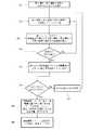
入力を終えたら、第1積層及び第2積層の各層に用いる材料の組み合わせを選択する(ステップS1)。例えば、第1積層及び第2積層はガラス基板側からZnS、MgF2、Al2O3の順からなる材料の組み合わせを選択する。When the input is completed, a combination of materials used for each layer of the first stack and the second stack is selected (step S1). For example, for the first stack and the second stack, a combination of materials consisting of ZnS, MgF2 , and Al2 O3 is selected from the glass substrate side.
次に、第1積層及び第2積層の各層の膜厚の初期値をランダムに決定する(ステップS2)。 Next, the initial value of the film thickness of each layer of the first stack and the second stack is randomly determined (step S2).
次に、準ニュートン法を用いて、発電電流を極大とする第1積層及び第2積層の各層の膜厚の局所的な最適解を算出する(ステップS3)。この局所的な最適解の算出は探索終了条件を満足するまで行う(ステップS4)。探索終了条件としては、ユーザが予め入力した指定回数に探索回数が達した場合を挙げることができる。他にも、現在までに行った探索の回数(k)と、実際に見つかった互いに異なる局所最適解の個数(NL)の関数として、局所最適解全体の個数の推定値(NE)を定義する(NE=f(NL、k))。そして、NL/NE>alphaとなったときに探索終了としてもよい。なおalphaはユーザが予め入力した値である。 Next, using the quasi-Newton method, the local optimum solution of the film thickness of each layer of the first stack and the second stack that maximizes the generated current is calculated (step S3). The calculation of the local optimum solution is performed until the search end condition is satisfied (step S4). An example of the search end condition is a case where the number of searches reaches the specified number of times input in advance by the user. In addition, an estimation value (NE) of the total number of local optimum solutions is defined as a function of the number of searches performed so far (k) and the number of different local optimum solutions actually found (NL). (NE = f (NL, k)). The search may be terminated when NL / NE> alpha. Note that alpha is a value input in advance by the user.
探索終了条件を満足したら(ステップS4;Yes)得られた局所最適解の中から発電電流の大きなn個(nは予め入力した値である)を準最適解リストとして記憶しておく(ステップS5)。このようなステップS2〜S5を全ての材料の組合せが終わるまで実行する。 If the search end condition is satisfied (step S4; Yes), n pieces of large generated currents (n is a value input in advance) among the obtained local optimum solutions are stored as a quasi-optimal solution list (step S5). ). Such steps S2 to S5 are executed until the combination of all materials is completed.
ここで、準ニュートン法を用いた局所最適解の探索に必要となる、発電電流の計算について詳細に説明する。図3に示すように、発電電流の計算においては、積層基板を(a)第1積層、(b)ガラス基板、(c)第2積層及び太陽電池(発電層)の3つに分割する。そして、(a)及び(c)については、マトリクス法を適用することで、(a)及び(c)の反射率及び透過率を計算する。 Here, the calculation of the generated current required for searching for the local optimum solution using the quasi-Newton method will be described in detail. As shown in FIG. 3, in the calculation of the generated current, the laminated substrate is divided into three parts: (a) a first laminated layer, (b) a glass substrate, (c) a second laminated layer, and a solar cell (power generating layer). And about (a) and (c), the reflectance and transmittance | permeability of (a) and (c) are calculated by applying the matrix method.
具体的には、プログラムに、ステップS1で定めた第1積層及び第2積層の各層の材料に対応する屈折率及び消衰係数をデータベースから検索させ、これらの屈折率、消衰係数、及びステップS2で定めた第1積層及び第2積層の各層の膜厚の初期値を元に、マトリクス法により(a)及び(b)の反射率及び透過率を計算させる。 Specifically, the program is made to retrieve from the database the refractive index and the extinction coefficient corresponding to the material of each layer of the first stack and the second stack determined in step S1, and the refractive index, the extinction coefficient, and the step Based on the initial values of the film thicknesses of the first and second layers determined in S2, the reflectance and transmittance of (a) and (b) are calculated by the matrix method.
外部から第1積層に向けて入射される入射光が第1積層を透過する透過率をTa、第1積層で反射する反射率をRaとする。ガラス基板から第1積層に向けて入射する入射光が第1積層を透過する透過率をTb、第1積層で反射する反射率をRbとする。ガラス基板から第2積層に向けて入射される入射光が第2積層を透過する透過率をTc、第2積層で反射する反射率をRcとする。上述したマトリクス法により、このRa,Ta,Rb,Tb,Rc,Tcが算出される。 It is assumed that the incident light incident from the outside toward the first stack is Ta, and the transmittance at which the first stack is reflected is Ra. The incident light incident from the glass substrate toward the first stack is Tb, and the reflectance at which the incident light is reflected by the first stack is Rb. The incident light incident from the glass substrate toward the second stack is defined as Tc, and the reflectance at which the second stack is reflected is represented by Rc. Ra, Ta, Rb, Tb, Rc, and Tc are calculated by the matrix method described above.
また、第2積層を透過する光が発電層において吸収される割合を計算する。具体的には、発電層に用いられる材料やその膜厚によりマトリクス法を用いて計算する。この割合をΨ(ポテンシャルトランスミッタンス)とする。さらに、ガラス基板の内部透過率Tpを算出する。この内部透過率Tpは、ガラス基板の膜厚から計算する。 In addition, the ratio of the light transmitted through the second stack that is absorbed in the power generation layer is calculated. Specifically, calculation is performed using a matrix method depending on the material used for the power generation layer and its film thickness. This ratio is defined as ψ (potential transmission). Furthermore, the internal transmittance Tp of the glass substrate is calculated. This internal transmittance Tp is calculated from the film thickness of the glass substrate.
積層基板においては、入射した光は、ガラス基板の表面、裏面(第1積層、第2積層との境界面)において多重反射する。このような多重反射を考慮して、発電層で吸収されるエネルギー量を算出する。発電層の吸収エネルギーA(光吸収量)は、次式により得られる。 In the laminated substrate, the incident light is multiple-reflected on the front surface and the back surface (boundary surface between the first laminated layer and the second laminated layer) of the glass substrate. The amount of energy absorbed by the power generation layer is calculated in consideration of such multiple reflection. The absorption energy A (light absorption amount) of the power generation layer is obtained by the following equation.
このような吸収エネルギーAは、入射する光の波長を変えて波長ごとに計算する。そして、波長毎の光吸収量を積分することで、総吸収エネルギー(総光吸収量)を算出する。この総吸収エネルギーと、表1に示した光電変換効率とを用いて、光子数に換算することにより、太陽電池で発生する発電電流を得ることができる。 Such absorption energy A is calculated for each wavelength by changing the wavelength of incident light. Then, the total absorption energy (total light absorption amount) is calculated by integrating the light absorption amount for each wavelength. By using this total absorbed energy and the photoelectric conversion efficiency shown in Table 1 and converting it to the number of photons, a power generation current generated in the solar cell can be obtained.
ここで、一般に、マトリクス法は、ミリメートルオーダーの膜厚を有するガラス基板には直接適用することができない。つまり、ミリメートルオーダーのガラス基板を含む積層基板全体は、マトリクス法を適用できないため、発電電流を算出することが困難である。 Here, in general, the matrix method cannot be directly applied to a glass substrate having a film thickness on the order of millimeters. That is, since the matrix method cannot be applied to the entire laminated substrate including the millimeter-order glass substrate, it is difficult to calculate the generated current.
しかしながら、本発明においては、上述したように、発電電流の算出に際しては、第1積層、第2積層、太陽電池に関してはマトリクス法を使用して光の反射率、透過率、ポテンシャルトランスミッタンスを算出し、ガラス基板に関しては膜厚から内部透過率を算出した。このように、従来のマトリクス法を直接適用したのでは光吸収量を算出できない積層基板についても、本発明においては、積層基板の構成を考慮してマトリクス法を適用し、発電電流を得ることが可能となった。 However, in the present invention, as described above, when the generated current is calculated, the first stack, the second stack, and the solar cell are calculated using the matrix method to calculate the light reflectance, transmittance, and potential transmitter. For the glass substrate, the internal transmittance was calculated from the film thickness. As described above, in the present invention, the matrix method can be applied in consideration of the configuration of the multilayer substrate to obtain the generated current even for the multilayer substrate in which the light absorption amount cannot be calculated by directly applying the conventional matrix method. It has become possible.
このようにして、ランダムな膜厚の初期値から始めて、準ニュートン法により発電電流が極大となるような第1積層及び第2積層の膜厚(局所最適解)を求めることが可能となった。1つの局所最適解が求まったら、別のランダムな膜厚の初期値を与えて、局所最適解を得る(図2;ステップS2〜S4の繰り返し)。このようにして得られた局所最適解は、準最適解リストとして記憶しておく(図2;ステップS5)。準最適解リストとは、発電電流の高いn個の局所最適解(第1積層及び第2積層の膜厚)の集合である。 In this way, starting from the initial value of the random film thickness, it has become possible to obtain the film thickness (local optimum solution) of the first stack and the second stack that maximize the generated current by the quasi-Newton method. . When one local optimum solution is obtained, an initial value of another random film thickness is given to obtain a local optimum solution (FIG. 2; repetition of steps S2 to S4). The local optimal solution obtained in this way is stored as a semi-optimal solution list (FIG. 2; step S5). The quasi-optimal solution list is a set of n local optimum solutions (film thicknesses of the first stack and the second stack) having a high generated current.
準最適解リストを得られた後、全ての材料の組み合わせが終了したかを判断する(ステップS6)。先に述べた例では、第1積層及び第2積層に適用可能な材料としてZnS、MgF2、Al2O3を指定した(表1参照)。そして、第1積層及び第2積層にはガラス基板側からZnS、MgF2、Al2O3の順からなる材料の組み合わせを選択した。したがって、それら以外の組み合わせについては、上述したステップS2〜S5の処理を行っていない。After the suboptimal solution list is obtained, it is determined whether or not all the material combinations have been completed (step S6). In the example described above, ZnS, MgF2 , and Al2 O3 were designated as materials applicable to the first stack and the second stack (see Table 1). Then, the first laminate and the second laminate was selected combinations of materials consisting of glass substrate sideZnS, from the order of
そこで、第1積層及び第2積層に適用する材料の組み合わせを変更し(ステップS7)、上述したステップS2〜S5の処理を行うことで、準最適解リストを更新する。そして、表1に示した入力値のうち、第1積層及び第2積層に適用可能な材料の全ての組み合わせについて、発電電力を算出し、準最適解リストを更新する。 Therefore, the combination of materials applied to the first stack and the second stack is changed (step S7), and the process of steps S2 to S5 described above is performed to update the semi-optimal solution list. Then, among the input values shown in Table 1, the generated power is calculated for all combinations of materials applicable to the first stack and the second stack, and the suboptimal solution list is updated.
このように、全ての材料の組み合わせについて全数探索を行い、各材料の組み合わせについて、膜厚及び屈折率の最適化を行った結果が準最適解リストとして得られる。そして、準最適解リストの中から発電電流量が最も高いものが最適解となる。このようなアルゴリズムをMultistartと称する。すなわち、Multistartとは、ランダムに選んだ多数の膜厚の初期値から準ニュートン法による局所的最適解の探索を繰り返し、得られた多数の局所的最適解(準最適解リスト)の中で最も良い解を最適解とするアルゴリズムである。このアルゴリズムによれば、大域的な最適解(又はそれに近い解)を高速に求めることができる。 In this way, the exhaustive search is performed for all combinations of materials, and the result of optimization of the film thickness and refractive index for each combination of materials is obtained as a semi-optimal solution list. Then, the one with the highest generated current amount from the sub-optimal solution list is the optimum solution. Such an algorithm is referred to as Multistart. In other words, Multistart is a search for a local optimum solution by a quasi-Newton method from a large number of randomly selected initial values of the film thickness, and the most of the obtained many local optimum solutions (sub-optimal solution list). It is an algorithm that makes a good solution an optimal solution. According to this algorithm, a global optimum solution (or a solution close thereto) can be obtained at high speed.
次のステップでは、準最適解リストの各局所最適解を、発電電流量の高い順に並び替えて、発電電流が大きいK個(Kは予め入力した値である)について、膜厚・屈折率の誤差による発電電流量の低下を計算する(ステップS8)。具体的には、表1に示した膜厚誤差を考慮する各層について、膜厚及び屈折率を膜厚誤差の大きさだけ変動させ、発電電流を計算する。この発電電流の計算は上述した方法(ステップS3)により行う。 In the next step, the local optimum solutions in the semi-optimal solution list are rearranged in descending order of the amount of generated current, and the film thickness / refractive index of K pieces (K is a value input in advance) with a large generated current. A reduction in the amount of generated current due to the error is calculated (step S8). Specifically, for each layer considering the film thickness error shown in Table 1, the film thickness and the refractive index are varied by the magnitude of the film thickness error, and the generated current is calculated. The calculation of the generated current is performed by the method described above (step S3).
例えば、第1積層及び第2積層がそれぞれ1層(a層、b層とする)であり、a層、b層の膜厚誤差が10nmとした場合、次の4つのケースについて発電電流量を計算する。
(1)a層の膜厚を10nm増加、b層の膜厚を10nm増加させた場合
(2)a層の膜厚を10nm増加、b層の膜厚を10nm減少させた場合
(3)a層の膜厚を10nm減少、b層の膜厚を10nm増加させた場合
(4)a層の膜厚を10nm減少、b層の膜厚を10nm減少させた場合For example, when the first stack and the second stack are each one layer (a layer and b layer), and the film thickness error of the a layer and the b layer is 10 nm, the generated current amount is set to the following four cases. calculate.
(1) When the thickness of the a layer is increased by 10 nm and when the thickness of the b layer is increased by 10 nm (2) When the thickness of the a layer is increased by 10 nm and when the thickness of the b layer is decreased by 10 nm (3) a When the layer thickness is decreased by 10 nm and the thickness of the b layer is increased by 10 nm (4) When the thickness of the a layer is decreased by 10 nm and the thickness of the b layer is decreased by 10 nm
これらの各ケースについての発電電流量を平均化したものと、誤差がない場合の発電電流量との差異を、膜厚誤差による発電電流量の低下と推定する。あるいは、発電電流量の低下量は、上記の各ケースについての発電電流量と、誤差が無い場合の発電電流の差の二乗平均の平方根をとってもよい。このように、あらかじめ指定された範囲内の様々な膜厚・屈折率の誤差を考慮した発電電流量と、誤差が無い場合の発電電流量との差を用いて、平均化等の統計的操作を行うことで、製造誤差が発電電流量に及ぼす影響を評価する。 The difference between the average of the generated current amount for each of these cases and the generated current amount when there is no error is estimated as a decrease in the generated current amount due to the film thickness error. Alternatively, the amount of decrease in the amount of generated current may be the square root of the root mean square of the difference between the amount of generated current for each of the above cases and the generated current when there is no error. In this way, statistical operations such as averaging are performed using the difference between the amount of generated current in consideration of various film thickness / refractive index errors within a pre-specified range and the amount of generated current when there is no error. To evaluate the effects of manufacturing errors on the amount of generated current.
そして、準最適解リストの内、製造誤差がある場合の影響を計算したK個の内容を、計算結果として出力する(ステップS9)。この出力例を表2に示す。 Then, in the sub-optimal solution list, K contents for which the influence when there is a manufacturing error is calculated are output as calculation results (step S9). Table 2 shows an example of this output.
表2に示すように、発電電流の高い順に5つ(n=5)の局所最適解が出力されている。発電電流量としては、絶対値ではなく、第1積層、第2積層が無い構造(ガラス基板の太陽電池のみの構造)における発電電流量との相対比である。 As shown in Table 2, five (n = 5) local optimum solutions are output in descending order of the generated current. The amount of generated current is not an absolute value but a relative ratio to the amount of generated current in a structure without a first stack and a second stack (a structure of only a solar cell on a glass substrate).
製造時の誤差を考慮しない場合(誤差無し)においては、最も発電電流量が高いものとしては+7.5%のNo.1の構成が例示される。すなわち、No.1が最適解として得られることになる。 When the error at the time of manufacture is not taken into consideration (no error), the highest generated current amount is + 7.5%. One configuration is exemplified. That is, no. 1 is obtained as the optimum solution.
一方、製造時の誤差を考慮した場合(誤差有り)においては、最も発電電流量が高いものとしては、+6.5%のNo.2の構成が例示される。つまり、製造時に膜厚が10nmの誤差(表1参照)が生じうることを考慮したとき、No.2では、+6.5%の発電電流量の増加が見込めることが分かる。一方、No.1は、誤差無しでは最適であるものの、誤差を考慮したら、+5.8%の発電電流量の増加となり、No.2よりも少ないことが分かる。 On the other hand, when the error at the time of manufacture is taken into account (with an error), the No. of + 6.5% is the highest generated current. Two configurations are exemplified. That is, when considering that an error with a film thickness of 10 nm (see Table 1) may occur at the time of manufacture, no. 2 shows that an increase in the amount of generated current of + 6.5% can be expected. On the other hand, no. No. 1 is optimal without error, but if the error is considered, the amount of generated current increases by + 5.8%. It can be seen that it is less than 2.
以上に説明した本発明の積層基板の製造支援方法及びプログラムによれば、太陽電池の性能上、最も重要な発電電流量を直接的に評価しているため、発電層における発電性能を十分に向上することができる積層基板の構成を得ることができる。 According to the manufacturing support method and program of the multilayer substrate of the present invention described above, the power generation performance in the power generation layer is sufficiently improved because the most important power generation current is directly evaluated on the performance of the solar cell. The structure of the laminated substrate that can be obtained can be obtained.
また、厚さがミリメートルオーダーのガラス基板を含む積層基板について、ガラス基板とそれ以外(第1積層、第2積層及び太陽電池)の両者を同時に扱った光の解析が可能となる。 In addition, for a laminated substrate including a glass substrate having a thickness of the order of millimeters, it is possible to analyze light in which both the glass substrate and the other substrates (first laminated layer, second laminated layer, and solar cell) are handled simultaneously.
さらに、本発明の積層基板の製造支援方法及びプログラムによれば、設計性能が最も良い最適解を出力するのみならず、膜厚や屈折率の製造誤差に対する性能低下レベルが小さい(ロバストである)準最適解をも出力することができる。これにより、製造誤差を考慮した上での最適な発電電流量を発揮できる積層基板の構成(第1積層及び第2積層の材料、膜厚及び屈折率)を得ることができる。 Furthermore, according to the manufacturing support method and program of the multilayer substrate of the present invention, not only the optimum solution with the best design performance is output, but also the performance degradation level with respect to the manufacturing error of the film thickness and the refractive index is small (robust). A suboptimal solution can also be output. Thereby, it is possible to obtain a configuration (a material of the first and second laminates, a film thickness and a refractive index) of the laminated substrate capable of exhibiting an optimal amount of generated current in consideration of manufacturing errors.
また、準最適解リストの表示としては、第1積層及び第2積層の材料を表示するのではなく、屈折率を表示するようにしてもよい。これにより、そのような屈折率を有する材料を任意に選ぶことが可能となる。 Further, as the display of the semi-optimal solution list, the refractive index may be displayed instead of displaying the materials of the first stack and the second stack. This makes it possible to arbitrarily select a material having such a refractive index.
さらに、本発明の積層基板の製造支援方法及びプログラムは、上述した太陽電池を含む積層基板にのみ適用可能なものではない。基板の両面に第1積層及び第2積層が設けられ、第1積層、基板及び第2積層を透過した光が第2積層側に設けられた光吸収層により吸収されるもの一般に適用可能である。 Furthermore, the manufacturing support method and program for the multilayer substrate of the present invention are not applicable only to the multilayer substrate including the solar cell described above. The first stack and the second stack are provided on both surfaces of the substrate, and the light transmitted through the first stack, the substrate, and the second stack is absorbed by the light absorption layer provided on the second stack side. .
ここで、本発明の積層基板の製造方法は、上述した積層基板の製造支援方法により得られた材料及び膜厚で積層基板を製造することを特徴とする。具体的な製造方法は、ガラス基板に各種材料からなる薄膜を成膜する公知の方法により行うことができる。この製造方法により得られた積層基板は、選択した材料の中で発電電流量(光吸収量)が最適(誤差無し又は誤差有り)となる。 Here, the manufacturing method of the multilayer substrate of the present invention is characterized in that the multilayer substrate is manufactured with the material and the film thickness obtained by the above-described multilayer substrate manufacturing support method. A specific manufacturing method can be performed by a known method of forming a thin film made of various materials on a glass substrate. The laminated substrate obtained by this manufacturing method has the optimum amount of generated current (light absorption amount) among the selected materials (no error or with error).
さらに、本発明の故障原因特定方法は、上述した積層基板の製造支援方法を用いて、積層基板を製造する過程での故障原因を特定することを特徴とする。たとえば、太陽電池用の積層基板を製造する過程において、それを用いて製造された太陽電池の発電性能が設計より低下してしまう故障の要因解析に効を奏する。つまり、太陽電池製造を目的とした第1積層及び第2積層に用いられる材料の薄膜形成工程において、各積層の各膜厚を評価し、その結果と、本発明に係る製造支援方法で得られた準最適解のリストとを照らし合わせ、どの積層での膜厚変動が性能低下により大きく影響しているかを把握することができ、もっとも影響の大きい層から膜厚変動を抑える努力をすることにおいて、効率的に太陽電池の性能低下故障の解消を図ることができる。 Furthermore, the failure cause identifying method of the present invention is characterized in that the cause of failure in the process of manufacturing a laminated substrate is specified using the above-described laminated substrate manufacturing support method. For example, in the process of manufacturing a laminated substrate for a solar cell, it is effective for analyzing the cause of a failure in which the power generation performance of the solar cell manufactured using the substrate is lower than the design. That is, in the thin film formation process of the material used for the first stack and the second stack for the purpose of manufacturing a solar cell, each film thickness of each stack is evaluated, and the result and the manufacturing support method according to the present invention are obtained. In comparison with the list of sub-optimal solutions, it is possible to grasp which film thickness fluctuation is greatly affected by the performance degradation, and in making an effort to suppress film thickness fluctuation from the most influential layer. Thus, it is possible to efficiently eliminate the performance degradation failure of the solar cell.
ここで、図1に示した積層基板1のうち、製造支援方法により得られた材料と膜厚を次のようにした積層基板が最適な発電電流量を有するものであった。 Here, among the
すなわち、第1積層は、ガラス基板の一方面上に、94〜114nmのAl2O3、0〜16nmのZnS、及び82〜102nmのMgF2を順次積層したものである。第2積層は、ガラス基板の他方面上に、134〜154nmのMgF2、125〜145nmのAl2O3、25〜45nmのMgF2を順次積層したものである。なお、第1層のZnSは、0nmすなわち無くても最適な発電電流量を有するものであった。That is, in the first stack, 94 to 114 nm of Al2 O3 , 0 to 16 nm of ZnS, and 82 to 102 nm of MgF2 are sequentially stacked on one surface of the glass substrate. In the second lamination, 134 to 154 nm MgF2 , 125 to 145 nm Al2 O3 , and 25 to 45 nm MgF2 are sequentially laminated on the other surface of the glass substrate. Note that the ZnS of the first layer had an optimum amount of generated current even if it was 0 nm, that is, it was not present.
なお、これらの第1積層及び第2積層に用いる材料は、一例として、Al2O3,Fe3O4,GeO2,Cu2O,TiO2,MnO3,SiO2,SnO2,ZnO,HfOx,Si,SiGe,SiC,a−Si,AlGaAs,GaAs,GaP,Ge,InGaAs,CdHg,Pb4,ITO,TiN,ZnSe,SiN,Pd,Zn,Moからなる材料群から選択されたものである。The materials used for the first and second stacks are, for example, Al2 O3 , Fe3 O4 , GeO2 , Cu2 O, TiO2 , MnO3 , SiO2 , SnO2 , ZnO, HfOx, those selected Si, SiGe, SiC, a- Si, AlGaAs, GaAs, GaP, Ge, InGaAs, CdHg,
さらに、図1に示した積層基板2のうち、製造支援方法により得られた屈折率と膜厚を次のようにした積層基板が最適な発電電流量を有するものであった。 Furthermore, among the
すなわち、第1積層は、ガラス基板の一方面上に、屈折率1.0〜1.1の材料を膜厚2〜22nmで形成した層、屈折率1.15〜1.35の材料を膜厚72〜92nmで形成した層、及び屈折率1.0〜1.8の材料を膜厚204〜224nmで形成した層を順次積層したものである。第2積層は、ガラス基板の他方面上に、屈折率2.09〜2.29の材料を膜厚108〜128nmで形成した層、屈折率1.01〜1.1の材料を膜厚20〜30nmで形成した層を順次積層したものである。 That is, the first laminate is a layer in which a material having a refractive index of 1.0 to 1.1 is formed with a film thickness of 2 to 22 nm on one surface of the glass substrate, and a material having a refractive index of 1.15 to 1.35. A layer formed with a thickness of 72 to 92 nm and a layer formed of a material with a refractive index of 1.0 to 1.8 with a thickness of 204 to 224 nm are sequentially stacked. The second laminate is a layer in which a material having a refractive index of 2.09 to 2.29 is formed on the other surface of the glass substrate with a film thickness of 108 to 128 nm, and a material having a refractive index of 1.01 to 1.1 is 20 in thickness. The layers formed at ˜30 nm are sequentially stacked.
本発明は、基板の両面に第1積層及び第2積層を設け、第2積層側に光吸収層を設けた積層基板の設計、製造等を行う産業分野で利用することができる。 INDUSTRIAL APPLICABILITY The present invention can be used in an industrial field in which a first laminated layer and a second laminated layer are provided on both sides of a substrate, and a laminated substrate having a light absorbing layer on the second laminated side is designed and manufactured.
1、2、3 積層基板1, 2, 3 Multilayer substrate
Claims (10)
Translated fromJapanese前記第1積層及び前記第2積層に用いる材料、並びに前記材料について光の波長に依存する屈折率及び消衰係数を用いて、前記第1積層側から光が入射した際の前記第1積層及び前記第2積層の反射率及び透過率をマトリクス法により求め、
前記基板の膜厚から当該基板の内部透過率を計算し、
前記第1積層及び前記第2積層の反射率及び透過率並びに前記内部透過率から、前記第1積層側に入射した光が前記光吸収層に吸収される光吸収量を波長ごとに計算し、該光吸収量を積分して総光吸収量を求め、
前記総光吸収量が最大となる前記第1積層及び前記第2積層の材料及び膜厚を求める
ことを特徴とする積層基板の製造支援方法。A substrate, a first stack and a second stack made of a plurality of materials, and a light absorption layer that absorbs light, wherein the first stack is provided on one surface of the substrate, and the second stack is formed on the substrate. Provided on the other surface, the light absorption layer is a manufacturing support method of a laminated substrate provided on the second laminate,
The material used for the first stack and the second stack, and the first stack when light is incident from the first stack side using the refractive index and extinction coefficient depending on the wavelength of light for the material. Obtaining the reflectance and transmittance of the second laminate by a matrix method,
Calculate the internal transmittance of the substrate from the thickness of the substrate,
From the reflectance and transmittance of the first stack and the second stack, and the internal transmittance, the amount of light absorbed by the light absorption layer by the light incident on the first stack is calculated for each wavelength. Integrating the light absorption amount to obtain the total light absorption amount,
A method for supporting the manufacture of a laminated substrate, comprising: obtaining a material and a film thickness of the first laminated layer and the second laminated layer that maximize the total light absorption amount.
前記総光吸収量が最大となる前記第1積層及び前記第2積層の膜厚を求める方法は、
前記第1積層及び前記第2積層の各膜厚に初期値として任意の数値を与え、準ニュートン法を用いて前記第1積層及び前記第2積層の膜厚の最適値を求め、
当該最適値を求める工程を複数回実行することで、複数の最適値からなる準最適値リストを求める
ことを特徴とする積層基板の製造支援方法。In the manufacturing support method of the multilayer substrate according to claim1 ,
The method of obtaining the film thickness of the first stack and the second stack that maximizes the total light absorption amount,
An arbitrary numerical value is given as an initial value to each film thickness of the first stack and the second stack, and an optimum value of the film thickness of the first stack and the second stack is obtained using a quasi-Newton method.
A manufacturing support method for a laminated substrate, wherein a sub-optimal value list including a plurality of optimum values is obtained by executing the step of obtaining the optimum values a plurality of times.
前記第1積層又は前記第2積層について得られた膜厚の最適値と、当該膜厚に対応する総光吸収量との対応を表示すると共に、当該膜厚を一定値で変動させたときの総光吸収量の変動を表示する
ことを特徴とする積層基板の製造支援方法。In the manufacturing support method of the multilayer substrate according toclaim 1or 2 ,
When the correspondence between the optimum value of the film thickness obtained for the first stack or the second stack and the total light absorption corresponding to the film thickness is displayed, and when the film thickness is varied by a constant value A method for supporting the production of a multilayer substrate, characterized by displaying a change in total light absorption.
当該材料及び膜厚の積層基板を製造する
ことを特徴とする積層基板の製造方法。Using the manufacturing support method for a multilayer substrate according to any one of claims 1 to3, a material and a film thickness used for the first stack and the second stack are determined,
A method for manufacturing a multilayer substrate, comprising: manufacturing the multilayer substrate having the material and film thickness.
前記基板としてガラス基板を用い、
前記ガラス基板の一方面上に、94〜114nmのアルミナ、0〜16nmのZnS、及び82〜102nmのMgF2を順次積層した前記第1積層を形成し、
前記ガラス基板の他方面上に、134〜154nmのMgF2、125〜145nmのアルミナ及び25〜45nmのMgF2を順次積層した前記第2積層を形成し、
前記第2積層上に、透明導電膜と太陽電池を設ける
ことを特徴とする積層基板の製造方法。In the manufacturing methodof the laminated substrate of Claim4 ,
Using a glass substrateas the substrate,
Before SL on one surface of a glass substrate,forming alumina 94~114Nm, ZnS of 0~16Nm, andthe first laminated sequentially laminating MgF2 of82~102Nm,
Before SL on the other surface of the glass substrate,MgF 2 of 134~154Nm,to form the second laminated sequentially laminating MgF2 of alumina and 25~45nm of125~145Nm,
A transparent conductive film and a solar cellare provided on the second stack. Amethod for manufacturing a stacked substrate.
前記基板としてガラス基板を用い、
前記ガラス基板の一方面上に、屈折率1.0〜1.1の材料を膜厚2〜22nmで形成した層、屈折率1.15〜1.35の材料を膜厚72〜92nmで形成した層、及び屈折率1.0〜1.8の材料を膜厚204〜224nmで形成した層を順次積層した前記第1積層を形成し、
前記ガラス基板の他方面上に、屈折率2.09〜2.29の材料を膜厚108〜128nmで形成した層、及び屈折率1.01〜1.1の材料を膜厚20〜30nmで形成した層を順次積層した前記第2積層を形成し、
前記第2積層上に、透明導電膜と太陽電池を設ける
ことを特徴とする積層基板の製造方法。In the manufacturing methodof the laminated substrate of Claim4 ,
Using a glass substrateas the substrate,
On one side of thefront Symbol glass substrate, a layer formed of the material having a refractive index 1.0 to 1.1 at a film thickness 2~22Nm, a material having a refractive index 1.15 to 1.35 in a thickness 72~92nm Formingthe first stack in which the formed layer and a layer formed of a material having a refractive index of 1.0 to 1.8 in a film thickness of 204 to 224 nm are sequentially stacked;
On the other side of thepre-Symbol glass substrate, the layer was formed of material of refractive index from 2.09 to 2.29 in thickness 108~128Nm, and thickness of material of refractive index 1.01-1.1 20 to 30 nm Formingthe second stack in which the layers formed in step 1 are sequentially stacked;
A transparent conductive film and a solar cellare provided on the second stack. Amethod for manufacturing a stacked substrate.
前記基板は、ガラス基板であり、
前記第1積層は、前記ガラス基板の一方面上に、94〜114nmのアルミナ、0〜16nmのZnS、及び82〜102nmのMgF2を順次積層したものであり、
前記第2積層は、前記ガラス基板の他方面上に、134〜154nmのMgF2、125〜145nmのアルミナ及び25〜45nmのMgF2を順次積層したものであり、
前記第2積層上に、透明導電膜と太陽電池が設けられている
ことを特徴とする積層基板。A laminated substrate in which a first laminate made of a plurality of materials is provided on one surface of the substrate, and a second laminate made of a plurality of materials is provided on the other surface of the substrate,
The substrate is a glass substrate;
The first stack is formed by sequentially stacking 94 to 114 nm of alumina, 0 to 16 nm of ZnS, and 82 to 102 nm of MgF2 on one surface of the glass substrate.
The second stack is on the other surface of the glass substrate,MgF 2 of 134~154Nm, are those which are sequentially stacked MgF2 of alumina and 25~45nm of 125~145Nm,
Multilayer substrate, characterized in that the secondproduct layer, a transparent conductive film and the solar cell are provided.
前記基板は、ガラス基板であり、
前記第1積層は、前記ガラス基板の一方面上に、屈折率1.0〜1.1の材料を膜厚2〜22nmで形成した層、屈折率1.15〜1.35の材料を膜厚72〜92nmで形成した層、及び屈折率1.0〜1.8の材料を膜厚204〜224nmで形成した層を順次
積層したものであり、
前記第2積層は、前記ガラス基板の他方面上に、屈折率2.09〜2.29の材料を膜厚108〜128nmで形成した層、及び屈折率1.01〜1.1の材料を膜厚20〜30nmで形成した層を順次積層したものであり、
前記第2積層上に、透明導電膜と太陽電池が設けられている
ことを特徴とする積層基板。A laminated substrate in which a first laminate made of a plurality of materials is provided on one surface of the substrate, and a second laminate made of a plurality of materials is provided on the other surface of the substrate,
The substrate is a glass substrate;
The first laminated layer is a layer in which a material having a refractive index of 1.0 to 1.1 is formed with a film thickness of 2 to 22 nm on one surface of the glass substrate, and a material having a refractive index of 1.15 to 1.35. A layer formed with a thickness of 72 to 92 nm and a layer formed with a material with a refractive index of 1.0 to 1.8 with a film thickness of 204 to 224 nm are sequentially stacked.
The second laminate includes a layer in which a material having a refractive index of 2.09 to 2.29 is formed with a film thickness of 108 to 128 nm and a material having a refractive index of 1.01 to 1.1 on the other surface of the glass substrate. Layers formed with a film thickness of 20 to 30 nm are sequentially stacked,
A transparent conductive film and a solar cell are provided on the second stacked layer.
Priority Applications (1)
| Application Number | Priority Date | Filing Date | Title |
|---|---|---|---|
| JP2012040741AJP5945886B2 (en) | 2012-02-27 | 2012-02-27 | Manufacturing support method for multilayer substrate, manufacturing method for multilayer substrate, failure cause identification method, manufacturing support program for multilayer substrate, and multilayer substrate |
Applications Claiming Priority (1)
| Application Number | Priority Date | Filing Date | Title |
|---|---|---|---|
| JP2012040741AJP5945886B2 (en) | 2012-02-27 | 2012-02-27 | Manufacturing support method for multilayer substrate, manufacturing method for multilayer substrate, failure cause identification method, manufacturing support program for multilayer substrate, and multilayer substrate |
Publications (2)
| Publication Number | Publication Date |
|---|---|
| JP2013175690A JP2013175690A (en) | 2013-09-05 |
| JP5945886B2true JP5945886B2 (en) | 2016-07-05 |
Family
ID=49268327
Family Applications (1)
| Application Number | Title | Priority Date | Filing Date |
|---|---|---|---|
| JP2012040741AActiveJP5945886B2 (en) | 2012-02-27 | 2012-02-27 | Manufacturing support method for multilayer substrate, manufacturing method for multilayer substrate, failure cause identification method, manufacturing support program for multilayer substrate, and multilayer substrate |
Country Status (1)
| Country | Link |
|---|---|
| JP (1) | JP5945886B2 (en) |
Families Citing this family (1)
| Publication number | Priority date | Publication date | Assignee | Title |
|---|---|---|---|---|
| CN115508932B (en)* | 2022-10-12 | 2025-05-30 | 广西泛华于成信息科技有限公司 | A dual-bandpass narrowband filter for gas detection and its manufacturing method |
Family Cites Families (13)
| Publication number | Priority date | Publication date | Assignee | Title |
|---|---|---|---|---|
| JPH0575156A (en)* | 1991-09-12 | 1993-03-26 | Mitsubishi Electric Corp | Solar cell |
| JP3900552B2 (en)* | 1996-07-11 | 2007-04-04 | 株式会社デンソー | Manufacturing method of optical sensor |
| JP3723392B2 (en)* | 1999-11-29 | 2005-12-07 | 大日本スクリーン製造株式会社 | Film thickness measuring apparatus and film thickness measuring method |
| FR2810118B1 (en)* | 2000-06-07 | 2005-01-21 | Saint Gobain Vitrage | TRANSPARENT SUBSTRATE HAVING ANTIREFLECTION COATING |
| JP3646158B2 (en)* | 2000-09-07 | 2005-05-11 | 独立行政法人産業技術総合研究所 | Dielectric multilayer dispersion compensating reflector |
| JP2002270879A (en)* | 2001-03-14 | 2002-09-20 | Mitsubishi Electric Corp | Semiconductor device |
| JP4245134B2 (en)* | 2003-01-30 | 2009-03-25 | パナソニック株式会社 | Mounting process simulation apparatus and mounting process simulation method |
| JP4856454B2 (en)* | 2006-03-16 | 2012-01-18 | 株式会社竹中工務店 | Solar cell installation evaluation device, solar cell installation evaluation program, and solar cell installation evaluation calculation method |
| WO2009085601A2 (en)* | 2007-12-21 | 2009-07-09 | Qualcom Mems Technologies, Inc. | Multijunction photovoltaic cells |
| US8716595B2 (en)* | 2008-03-24 | 2014-05-06 | The University Of Houston | Boron nitride anti-reflection coatings and methods |
| JPWO2010023867A1 (en)* | 2008-08-25 | 2012-01-26 | 株式会社エバテック | Thin film solar cell, method for manufacturing the same, and substrate for thin film solar cell |
| JP2011049460A (en)* | 2009-08-28 | 2011-03-10 | Mitsubishi Heavy Ind Ltd | Photoelectric converter and substrate with transparent electrode layer |
| US8895838B1 (en)* | 2010-01-08 | 2014-11-25 | Magnolia Solar, Inc. | Multijunction solar cell employing extended heterojunction and step graded antireflection structures and methods for constructing the same |
- 2012
- 2012-02-27JPJP2012040741Apatent/JP5945886B2/enactiveActive
Also Published As
| Publication number | Publication date |
|---|---|
| JP2013175690A (en) | 2013-09-05 |
Similar Documents
| Publication | Publication Date | Title |
|---|---|---|
| Bermel et al. | Improving thin-film crystalline silicon solar cell efficiencies with photonic crystals | |
| Schneider et al. | Pyramidal surface textures for light trapping and antireflection in perovskite-on-silicon tandem solar cells | |
| Meng et al. | Combined front and back diffraction gratings for broad band light trapping in thin film solar cell | |
| Jäger et al. | Prospects of light management in perovskite/silicon tandem solar cells | |
| Altazin et al. | Design of perovskite/crystalline-silicon monolithic tandem solar cells | |
| Filipič et al. | CH_3NH_3PbI_3 perovskite/silicon tandem solar cells: characterization based optical simulations | |
| Agrawal et al. | Broadband optical absorption enhancement through coherent light trapping in thin-film photovoltaic cells | |
| Fahr et al. | Approaching the Lambertian limit in randomly textured thin-film solar cells | |
| Yahaya et al. | Characterization of light absorption in thin-film silicon with periodic nanohole arrays | |
| US20120042948A1 (en) | Thin-film solar cell and manufacture method thereof | |
| Jang et al. | Antireflective property of thin film a-Si solar cell structures with graded refractive index structure | |
| Oh et al. | Enhanced broadband and omni-directional performance of polycrystalline Si solar cells by using discrete multilayer antireflection coatings | |
| Kim et al. | Silicon nanodisk array design for effective light trapping in ultrathin c-Si | |
| Leem et al. | Broadband antireflective germanium surfaces based on subwavelength structures for photovoltaic cell applications | |
| Hoffmann et al. | Advancing tandem solar cells by spectrally selective multilayer intermediate reflectors | |
| Kuo et al. | Quantum efficiency enhancement in selectively transparent silicon thin film solar cells by distributed Bragg reflectors | |
| US20120048374A1 (en) | Thin film solar cell and manufacturing method thereof | |
| Han et al. | Surface antireflection properties of GaN nanostructures with various effective refractive index profiles | |
| Yang et al. | High-efficiency photon capturing in ultrathin silicon solar cells with front nanobowl texture and truncated-nanopyramid reflector | |
| Cozza et al. | Optical modeling and optimizations of Cu_2ZnSnSe_4 solar cells using the modified transfer matrix method | |
| Vismara et al. | Back-contacted basi_2 solar cells: An optical study | |
| Goldman et al. | Nanophotonic resonators for InP solar cells | |
| O’Brien et al. | Photonic crystal intermediate reflectors for micromorph solar cells: a comparative study | |
| Wang et al. | Highly-ordered vertical Si nanowire/nanowall decorated solar cells | |
| Kowalczewski et al. | Silicon solar cells reaching the efficiency limits: from simple to complex modelling |
Legal Events
| Date | Code | Title | Description |
|---|---|---|---|
| A621 | Written request for application examination | Free format text:JAPANESE INTERMEDIATE CODE: A621 Effective date:20150223 | |
| A521 | Request for written amendment filed | Free format text:JAPANESE INTERMEDIATE CODE: A523 Effective date:20150312 | |
| RD04 | Notification of resignation of power of attorney | Free format text:JAPANESE INTERMEDIATE CODE: A7424 Effective date:20150422 | |
| A521 | Request for written amendment filed | Free format text:JAPANESE INTERMEDIATE CODE: A523 Effective date:20150420 | |
| A977 | Report on retrieval | Free format text:JAPANESE INTERMEDIATE CODE: A971007 Effective date:20151130 | |
| A131 | Notification of reasons for refusal | Free format text:JAPANESE INTERMEDIATE CODE: A131 Effective date:20151209 | |
| A521 | Request for written amendment filed | Free format text:JAPANESE INTERMEDIATE CODE: A523 Effective date:20160208 | |
| TRDD | Decision of grant or rejection written | ||
| A01 | Written decision to grant a patent or to grant a registration (utility model) | Free format text:JAPANESE INTERMEDIATE CODE: A01 Effective date:20160420 | |
| A61 | First payment of annual fees (during grant procedure) | Free format text:JAPANESE INTERMEDIATE CODE: A61 Effective date:20160518 | |
| R150 | Certificate of patent or registration of utility model | Ref document number:5945886 Country of ref document:JP Free format text:JAPANESE INTERMEDIATE CODE: R150 | |
| S111 | Request for change of ownership or part of ownership | Free format text:JAPANESE INTERMEDIATE CODE: R313117 | |
| S531 | Written request for registration of change of domicile | Free format text:JAPANESE INTERMEDIATE CODE: R313531 | |
| R350 | Written notification of registration of transfer | Free format text:JAPANESE INTERMEDIATE CODE: R350 | |
| R250 | Receipt of annual fees | Free format text:JAPANESE INTERMEDIATE CODE: R250 | |
| S531 | Written request for registration of change of domicile | Free format text:JAPANESE INTERMEDIATE CODE: R313531 | |
| R350 | Written notification of registration of transfer | Free format text:JAPANESE INTERMEDIATE CODE: R350 | |
| S111 | Request for change of ownership or part of ownership | Free format text:JAPANESE INTERMEDIATE CODE: R313117 | |
| R350 | Written notification of registration of transfer | Free format text:JAPANESE INTERMEDIATE CODE: R350 | |
| R250 | Receipt of annual fees | Free format text:JAPANESE INTERMEDIATE CODE: R250 | |
| R250 | Receipt of annual fees | Free format text:JAPANESE INTERMEDIATE CODE: R250 | |
| R250 | Receipt of annual fees | Free format text:JAPANESE INTERMEDIATE CODE: R250 | |
| R250 | Receipt of annual fees | Free format text:JAPANESE INTERMEDIATE CODE: R250 |