JP5939752B2 - Wafer dividing method - Google Patents
Wafer dividing methodDownload PDFInfo
- Publication number
- JP5939752B2 JP5939752B2JP2011190647AJP2011190647AJP5939752B2JP 5939752 B2JP5939752 B2JP 5939752B2JP 2011190647 AJP2011190647 AJP 2011190647AJP 2011190647 AJP2011190647 AJP 2011190647AJP 5939752 B2JP5939752 B2JP 5939752B2
- Authority
- JP
- Japan
- Prior art keywords
- wafer
- etching
- modified layer
- resistant mask
- forming step
- Prior art date
- Legal status (The legal status is an assumption and is not a legal conclusion. Google has not performed a legal analysis and makes no representation as to the accuracy of the status listed.)
- Active
Links
Images


Classifications
- H—ELECTRICITY
- H01—ELECTRIC ELEMENTS
- H01L—SEMICONDUCTOR DEVICES NOT COVERED BY CLASS H10
- H01L21/00—Processes or apparatus adapted for the manufacture or treatment of semiconductor or solid state devices or of parts thereof
- H01L21/02—Manufacture or treatment of semiconductor devices or of parts thereof
- H01L21/04—Manufacture or treatment of semiconductor devices or of parts thereof the devices having potential barriers, e.g. a PN junction, depletion layer or carrier concentration layer
- H01L21/18—Manufacture or treatment of semiconductor devices or of parts thereof the devices having potential barriers, e.g. a PN junction, depletion layer or carrier concentration layer the devices having semiconductor bodies comprising elements of Group IV of the Periodic Table or AIIIBV compounds with or without impurities, e.g. doping materials
- H01L21/30—Treatment of semiconductor bodies using processes or apparatus not provided for in groups H01L21/20 - H01L21/26
- H01L21/302—Treatment of semiconductor bodies using processes or apparatus not provided for in groups H01L21/20 - H01L21/26 to change their surface-physical characteristics or shape, e.g. etching, polishing, cutting
- H01L21/306—Chemical or electrical treatment, e.g. electrolytic etching
- H01L21/3065—Plasma etching; Reactive-ion etching
- B—PERFORMING OPERATIONS; TRANSPORTING
- B23—MACHINE TOOLS; METAL-WORKING NOT OTHERWISE PROVIDED FOR
- B23K—SOLDERING OR UNSOLDERING; WELDING; CLADDING OR PLATING BY SOLDERING OR WELDING; CUTTING BY APPLYING HEAT LOCALLY, e.g. FLAME CUTTING; WORKING BY LASER BEAM
- B23K26/00—Working by laser beam, e.g. welding, cutting or boring
- B23K26/352—Working by laser beam, e.g. welding, cutting or boring for surface treatment
- B23K26/3568—Modifying rugosity
- B—PERFORMING OPERATIONS; TRANSPORTING
- B23—MACHINE TOOLS; METAL-WORKING NOT OTHERWISE PROVIDED FOR
- B23K—SOLDERING OR UNSOLDERING; WELDING; CLADDING OR PLATING BY SOLDERING OR WELDING; CUTTING BY APPLYING HEAT LOCALLY, e.g. FLAME CUTTING; WORKING BY LASER BEAM
- B23K26/00—Working by laser beam, e.g. welding, cutting or boring
- B23K26/36—Removing material
- B23K26/362—Laser etching
- B23K26/364—Laser etching for making a groove or trench, e.g. for scribing a break initiation groove
- B—PERFORMING OPERATIONS; TRANSPORTING
- B23—MACHINE TOOLS; METAL-WORKING NOT OTHERWISE PROVIDED FOR
- B23K—SOLDERING OR UNSOLDERING; WELDING; CLADDING OR PLATING BY SOLDERING OR WELDING; CUTTING BY APPLYING HEAT LOCALLY, e.g. FLAME CUTTING; WORKING BY LASER BEAM
- B23K26/00—Working by laser beam, e.g. welding, cutting or boring
- B23K26/36—Removing material
- B23K26/40—Removing material taking account of the properties of the material involved
- B—PERFORMING OPERATIONS; TRANSPORTING
- B23—MACHINE TOOLS; METAL-WORKING NOT OTHERWISE PROVIDED FOR
- B23K—SOLDERING OR UNSOLDERING; WELDING; CLADDING OR PLATING BY SOLDERING OR WELDING; CUTTING BY APPLYING HEAT LOCALLY, e.g. FLAME CUTTING; WORKING BY LASER BEAM
- B23K26/00—Working by laser beam, e.g. welding, cutting or boring
- B23K26/50—Working by transmitting the laser beam through or within the workpiece
- B23K26/53—Working by transmitting the laser beam through or within the workpiece for modifying or reforming the material inside the workpiece, e.g. for producing break initiation cracks
- B—PERFORMING OPERATIONS; TRANSPORTING
- B28—WORKING CEMENT, CLAY, OR STONE
- B28D—WORKING STONE OR STONE-LIKE MATERIALS
- B28D5/00—Fine working of gems, jewels, crystals, e.g. of semiconductor material; apparatus or devices therefor
- H—ELECTRICITY
- H01—ELECTRIC ELEMENTS
- H01L—SEMICONDUCTOR DEVICES NOT COVERED BY CLASS H10
- H01L21/00—Processes or apparatus adapted for the manufacture or treatment of semiconductor or solid state devices or of parts thereof
- H01L21/02—Manufacture or treatment of semiconductor devices or of parts thereof
- H01L21/04—Manufacture or treatment of semiconductor devices or of parts thereof the devices having potential barriers, e.g. a PN junction, depletion layer or carrier concentration layer
- H01L21/18—Manufacture or treatment of semiconductor devices or of parts thereof the devices having potential barriers, e.g. a PN junction, depletion layer or carrier concentration layer the devices having semiconductor bodies comprising elements of Group IV of the Periodic Table or AIIIBV compounds with or without impurities, e.g. doping materials
- H01L21/30—Treatment of semiconductor bodies using processes or apparatus not provided for in groups H01L21/20 - H01L21/26
- H01L21/302—Treatment of semiconductor bodies using processes or apparatus not provided for in groups H01L21/20 - H01L21/26 to change their surface-physical characteristics or shape, e.g. etching, polishing, cutting
- H01L21/306—Chemical or electrical treatment, e.g. electrolytic etching
- H01L21/30604—Chemical etching
- H01L21/30608—Anisotropic liquid etching
- H—ELECTRICITY
- H01—ELECTRIC ELEMENTS
- H01L—SEMICONDUCTOR DEVICES NOT COVERED BY CLASS H10
- H01L21/00—Processes or apparatus adapted for the manufacture or treatment of semiconductor or solid state devices or of parts thereof
- H01L21/70—Manufacture or treatment of devices consisting of a plurality of solid state components formed in or on a common substrate or of parts thereof; Manufacture of integrated circuit devices or of parts thereof
- H01L21/77—Manufacture or treatment of devices consisting of a plurality of solid state components or integrated circuits formed in, or on, a common substrate
- H01L21/78—Manufacture or treatment of devices consisting of a plurality of solid state components or integrated circuits formed in, or on, a common substrate with subsequent division of the substrate into plural individual devices
- B—PERFORMING OPERATIONS; TRANSPORTING
- B23—MACHINE TOOLS; METAL-WORKING NOT OTHERWISE PROVIDED FOR
- B23K—SOLDERING OR UNSOLDERING; WELDING; CLADDING OR PLATING BY SOLDERING OR WELDING; CUTTING BY APPLYING HEAT LOCALLY, e.g. FLAME CUTTING; WORKING BY LASER BEAM
- B23K2101/00—Articles made by soldering, welding or cutting
- B23K2101/36—Electric or electronic devices
- B23K2101/40—Semiconductor devices
- B—PERFORMING OPERATIONS; TRANSPORTING
- B23—MACHINE TOOLS; METAL-WORKING NOT OTHERWISE PROVIDED FOR
- B23K—SOLDERING OR UNSOLDERING; WELDING; CLADDING OR PLATING BY SOLDERING OR WELDING; CUTTING BY APPLYING HEAT LOCALLY, e.g. FLAME CUTTING; WORKING BY LASER BEAM
- B23K2103/00—Materials to be soldered, welded or cut
- B23K2103/50—Inorganic material, e.g. metals, not provided for in B23K2103/02 – B23K2103/26
Landscapes
- Engineering & Computer Science (AREA)
- Physics & Mathematics (AREA)
- Optics & Photonics (AREA)
- Plasma & Fusion (AREA)
- Mechanical Engineering (AREA)
- Computer Hardware Design (AREA)
- General Physics & Mathematics (AREA)
- Manufacturing & Machinery (AREA)
- Condensed Matter Physics & Semiconductors (AREA)
- Microelectronics & Electronic Packaging (AREA)
- Power Engineering (AREA)
- Chemical & Material Sciences (AREA)
- Chemical Kinetics & Catalysis (AREA)
- General Chemical & Material Sciences (AREA)
- Oil, Petroleum & Natural Gas (AREA)
- Dicing (AREA)
- Laser Beam Processing (AREA)
Description
Translated fromJapanese本発明は、各種ウェーハを個々のチップに分割するウェーハの分割方法に関する。 The present invention relates to a wafer dividing method for dividing various wafers into individual chips.
IC、LSI等のデバイスが分割予定ラインによって区画されて表面に形成されたウェーハは、個々のデバイスに分割され、携帯電話機、パソコン等の各種電気機器等に利用されている。 Wafers formed on the surface by dividing devices such as IC and LSI by dividing lines are divided into individual devices and used for various electric devices such as mobile phones and personal computers.
ウェーハを個々のデバイスに分割する方法として、ウェーハに対して透過性を有する波長のレーザー光線を分割予定ラインの内部に集光することにより分割予定ラインに沿って改質層を形成し、その後、ウェーハに対して外力を加えることにより、改質層を起点としてデバイスに分割する技術が提案され、実用に供されている(例えば特許文献1参照)。 As a method of dividing a wafer into individual devices, a modified layer is formed along the planned dividing line by condensing a laser beam having a wavelength transparent to the wafer inside the planned dividing line. By applying an external force, a technique for dividing a modified layer into devices from a modified layer has been proposed and put into practical use (see, for example, Patent Document 1).
しかし、ウェーハに外力を加えて個々のデバイスに分割すると、改質層が粉砕されるため、微粉末がデバイスの表面に付着し、デバイスの品質を低下させるという問題がある。 However, when an external force is applied to the wafer to divide the wafer into individual devices, the modified layer is pulverized, so that there is a problem that the fine powder adheres to the surface of the device and the quality of the device is lowered.
また、ウェーハの分割後は改質層がデバイスの側面に残存するため、残存した改質層がデバイスの抗折強度を低下させるという問題がある。 Further, since the modified layer remains on the side surface of the device after the wafer is divided, there is a problem that the remaining modified layer reduces the bending strength of the device.
本発明は、このような問題にかんがみなされたもので、レーザー光線の照射によりウェーハの内部に改質層を形成し、改質層を起点としてウェーハを個々のデバイスに分割する場合において、デバイスの品質および抗折強度を低下させないようにすることを課題とする。 The present invention has been considered in view of such problems. In the case where a modified layer is formed inside a wafer by irradiation with a laser beam, and the wafer is divided into individual devices starting from the modified layer, the quality of the device is improved. Another object is to prevent the bending strength from being lowered.
本発明は、複数のデバイスが分割予定ラインによって区画されて表面に形成されたウェーハを個々のデバイスに分割するウェーハの分割方法に関し、ウェーハに対して透過性を有する波長のレーザー光線の集光点を分割予定ラインの内部に位置づけて照射し、分割予定ラインの内部にウェーハの表面側から裏面側に至る改質層を形成する改質層形成工程と、ウェーハをエッチングするエッチングガスまたはエッチング液をウェーハに供給し、改質層を侵食させてウェーハを個々のデバイスに分割するエッチング工程と、から少なくとも構成され、改質層形成工程の前にウェーハの表面に保護部材を貼着し、耐エッチングマスクをウェーハの裏面に被覆し分割予定ラインに沿って耐エッチングマスクを除去してウェーハ裏面を露出させる溝を形成する耐エッチングマスク形成工程が含まれる。The present invention relates to a wafer dividing method in which a plurality of devices are partitioned by a predetermined dividing line and a wafer formed on the surface is divided into individual devices, and a condensing point of a laser beam having a wavelength having transparency to the wafer is provided. A modified layer forming step for forming a modified layer from the front surface side to the back surface side of the wafer within the planned dividing line and irradiating it within the planned dividing line, and an etching gas or etching solution for etching the wafer. And an etching process in which the modified layer is eroded to divide the wafer into individual devices,and a protective member is attached to the surface of the wafer before the modified layer forming process. A groove that exposes the backside of the wafer by covering the backside of the wafer and removing the anti-etching mask along the planned dividing line It includes anti-etching mask forming process of the.
また、本発明は、複数のデバイスが分割予定ラインによって区画されて表面に形成されたウェーハを個々のデバイスに分割するウェーハの分割方法であって、ウェーハに対して透過性を有する波長のレーザー光線の集光点を分割予定ラインの内部に位置づけて照射し、分割予定ラインの内部にウェーハの表面側から裏面側に至る改質層を形成する改質層形成工程と、ウェーハをエッチングするエッチングガスまたはエッチング液をウェーハに供給し、改質層を侵食させてウェーハを個々のデバイスに分割するエッチング工程と、から少なくとも構成され、改質層形成工程の前にウェーハの裏面に保護部材を貼着し、耐エッチングマスクをウェーハの表面に被覆し分割予定ラインに沿って耐エッチングマスクを除去してウェーハ表面を露出させる溝を形成する耐エッチングマスク形成工程が含まれる。The present invention also relates to a wafer dividing method for dividing a wafer formed on a surface by dividing a plurality of devices into lines to be divided into individual devices, the laser beam having a wavelength having transparency to the wafer. A focused layer is positioned inside the planned dividing line and irradiated, and a modified layer forming step for forming a modified layer from the front side to the back side of the wafer inside the planned dividing line, and an etching gas for etching the wafer or An etching process that supplies an etchant to the wafer, erodes the modified layer, and divides the wafer into individual devices, and a protective member is attached to the back surface of the wafer before the modified layer forming process. Then, cover the surface of the wafer with an anti-etching mask and remove the anti-etching mask along the planned dividing line to expose the wafer surface. It includes anti-etching mask formation step of forming a groove.
上記発明において、耐エッチングマスク形成工程では、ダイシング又はレーザー照射により分割予定ラインに沿って耐エッチングマスクを除去して溝を形成し、改質層形成工程では、溝を介してレーザー光線を照射するとよい。In the above invention, in the etching resistant mask forming step, the etching resistant mask is removed along the planned dividing line by dicing or laser irradiation to form a groove, and in the modified layer forming step, the laser beam may be irradiated through the groove. .
本発明では、エッチング工程においてエッチングガスまたはエッチング液によって改質層を侵食させるようにしたことで、改質層が粉砕されないため、微粉末を発生させずにデバイスに分割することができる。したがって、微粉末がデバイスの表面に付着してデバイスの品質を低下させることがない。 In the present invention, since the modified layer is eroded by the etching gas or the etchant in the etching process, the modified layer is not crushed, and thus can be divided into devices without generating fine powder. Therefore, the fine powder does not adhere to the surface of the device and deteriorate the quality of the device.
また、エッチングによって改質層が除去されるため、改質層の残存に起因するデバイスの抗折強度の低下を防止することができる。 In addition, since the modified layer is removed by etching, it is possible to prevent a decrease in the bending strength of the device due to the remaining of the modified layer.
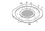
1 第1の実施形態
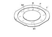
図1に示すウェーハWにおいては、表面W1に、縦横に分割予定ラインLが形成されている。そして、分割予定ラインLによって区画された領域には、デバイスDが複数形成されている。1 1st Embodiment In the wafer W shown in FIG. 1, the division | segmentation scheduled line L is formed in the surface W1 vertically and horizontally. A plurality of devices D are formed in the area partitioned by the division lines L.
(1)保護部材貼着工程
このウェーハWを裏返し、図2に示すように、表面W1を粘着テープ等からなる保護部材Pに貼着する。保護部材Pの周縁部にはリング状に形成されたフレームFが貼着されており、ウェーハWは、保護部材Pを介してフレームFに支持される。このとき、ウェーハWの裏面W2が露出した状態となる。(1) Protection member sticking process This wafer W is turned over and the surface W1 is stuck to the protection member P which consists of adhesive tapes etc., as shown in FIG. A frame F formed in a ring shape is attached to the periphery of the protection member P, and the wafer W is supported by the frame F via the protection member P. At this time, the back surface W2 of the wafer W is exposed.
(2)改質層形成工程
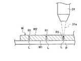
次に、このウェーハWに対してレーザー光線を照射し、分割予定ラインLに沿って、その内部に改質層を形成する。改質層の形成には、例えば図3に示すレーザー加工装置1を使用することができる。(2) Modified Layer Formation Step Next, the wafer W is irradiated with a laser beam, and a modified layer is formed along the division line L. For example, a laser processing apparatus 1 shown in FIG. 3 can be used to form the modified layer.
このレーザー加工装置1は、被加工物を保持するチャックテーブル2と、チャックテーブル2に保持された被加工物に対してレーザー光線を照射するレーザー照射手段3とを備えている。 The laser processing apparatus 1 includes a chuck table 2 that holds a workpiece, and a
保持手段2は、ウェーハWを吸引保持する保持面20と、フレームFを固定する固定部21とから構成されている。固定部21は、フレームFを上方から押圧する押さえ部210を備えている。 The holding unit 2 includes a
保持手段2は、加工送り手段4によって加工送り方向(X軸方向)に移動可能に支持されているとともに、割り出し送り手段5によってX軸方向に対して水平方向に直交する割り出し送り方向(Y軸方向)に移動可能に支持されている。加工送り手段4及び割り出し送り手段5は、制御手段6によって制御される。 The holding means 2 is supported by the machining feed means 4 so as to be movable in the machining feed direction (X-axis direction), and the index feed direction (Y-axis) orthogonal to the X-axis direction by the index feed means 5. Direction). The processing feed means 4 and the index feed means 5 are controlled by the control means 6.
加工送り手段4は、平板状の基台53上に配設され、X軸方向の軸心を有するボールネジ40と、ボールネジ40と平行に配設された一対のガイドレール41と、ボールネジ40の一端に連結されたモータ42と、図示しない内部のナットがボールネジ40に螺合すると共に下部がガイドレール41に摺接するスライド部43とから構成されている。この加工送り手段4は、制御手段6による制御の下でモータ42に駆動されてボールネジ40が回動するのに伴い、スライド部43がガイドレール41上をX軸方向に摺動して保持手段2をX軸方向に移動させる構成となっている。 The processing feed means 4 is disposed on a
保持手段2及び加工送り手段4は、割り出し送り手段5によってY軸方向に移動可能に支持されている。割り出し送り手段5は、Y軸方向の軸心を有するボールネジ50と、ボールネジ50に平行に配設された一対のガイドレール51と、ボールネジ50の一端に連結されたモータ52と、図示しない内部のナットがボールネジ50に螺合すると共に下部がガイドレール51に摺接する基台53とから構成されている。この割り出し送り手段5は、制御手段6による制御の下でモータ52に駆動されてボールネジ50が回動するのに伴い、基台53がガイドレール51上をY軸方向に摺動して保持手段2及び加工送り手段4をY軸方向に移動させる構成となっている。 The holding means 2 and the processing feed means 4 are supported by the index feed means 5 so as to be movable in the Y-axis direction. The index feeding means 5 includes a
レーザー照射手段3は、壁部10に固定された基台30と、基台30の先端部に固定された照射ヘッド31とを備えている。照射ヘッド31は、鉛直方向の光軸を有するレーザー光線を照射する機能を有しており、集光レンズを備えている。 The laser irradiation means 3 includes a
保持手段2においては、保護部材Pを介してウェーハWが保持面20に吸引保持され、フレームFが固定部21に固定される。そして、図示しないカメラによる撮像によってウェーハWの表面W1を撮像し、分割予定ラインLを検出する。なお、カメラがウェーハWの裏面W2側に位置する本発明の場合は、赤外線カメラを用いて裏面W2側から透過させて表面W1を撮像する。 In the holding means 2, the wafer W is sucked and held on the
分割予定ラインLの検出後、その分割予定ラインLと照射ヘッド31のY軸方向の位置をあわせる。そして、図4に示すように、保持手段2に保持されたウェーハWをX軸方向に送りながら、ウェーハWに対して透過性を有する波長のレーザー光線31aを照射ヘッド31から分割予定ラインLに沿って照射する。レーザー光線31aは、分割予定ラインLの内部の集光点に集光する。例えば以下の加工条件にてレーザー照射を行う。
レーザー光線の波長: 1064[nm]
平均出力: 0.3[W]
繰り返し周波数: 100[kHz]
スポット径: 1[μm]
送り速度: 100[mm/秒]After detecting the planned division line L, the division planned line L and the position of the
Laser beam wavelength: 1064 [nm]
Average output: 0.3 [W]
Repetition frequency: 100 [kHz]
Spot diameter: 1 [μm]
Feeding speed: 100 [mm / sec]
このような加工条件の下で分割予定ラインLの内部にレーザー光線を集光すると、図5に示すように、分割予定ラインLに沿ってウェーハWの内部に表面W1側から裏面W2側に至る改質層R1が形成される。改質層R1の形成時は、必要に応じて集光点をウェーハWの厚さ方向に移動させることにより、改質層R1の深さを調整する。 When the laser beam is condensed inside the planned division line L under such processing conditions, the modification from the front surface W1 side to the back surface W2 side inside the wafer W along the planned division line L as shown in FIG. A quality layer R1 is formed. When forming the modified layer R1, the depth of the modified layer R1 is adjusted by moving the condensing point in the thickness direction of the wafer W as necessary.
同様に、保持手段2のY軸方向の割り出し送りとともに、順次分割予定ラインLに沿ってレーザー照射を行い、さらに、保持手段2を90度回転させてから同様のレーザー照射を行うと、図6に示すように、すべての分割予定ラインLに沿って、その内部に改質層R1が形成される。 Similarly, when the holding unit 2 is indexed and fed in the Y-axis direction, laser irradiation is sequentially performed along the scheduled division line L, and when the same laser irradiation is performed after the holding unit 2 is rotated 90 degrees, FIG. As shown in FIG. 5, along all the planned division lines L, the modified layer R1 is formed therein.
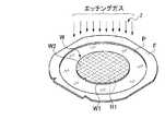
(3)エッチング工程
このようにしてすべての分割予定ラインLに沿って改質層R1が形成された後、図6に示すように、裏面W2側からエッチングガス7を供給して裏面W2側に対してドライエッチングを行う。図示していないが、エッチングガス7の供給は、密閉された真空室内で行う。エッチングガスとしては、例えばプラズマ化したSF6(六フッ化硫黄)を使用する。(3) Etching Step After the modified layer R1 is formed along all the planned division lines L in this way, as shown in FIG. 6, the
そうすると、図7及び図8に示すように、改質層R1に沿ってエッチングガスによる侵食が行われ、改質層R1が除去され、改質層R1が形成されていた部分に溝G1が形成され、溝G1によって個々のデバイスDに分割される。 Then, as shown in FIGS. 7 and 8, erosion by the etching gas is performed along the modified layer R1, the modified layer R1 is removed, and a groove G1 is formed in the portion where the modified layer R1 was formed. And divided into individual devices D by the grooves G1.
なお、エッチングガスによるドライエッチングに代えて、エッチング液によるウェットエッチングを用いることもできる。ウェットエッチングの場合は、ウェーハWをエッチング液、例えばKOH(水酸化カリウム)に浸漬する。なお、ウェーハWの裏面W2もエッチングされるが、改質層R1の方がエッチング速度が速いため、問題にはならない。 Note that wet etching using an etchant may be used instead of dry etching using an etching gas. In the case of wet etching, the wafer W is immersed in an etching solution such as KOH (potassium hydroxide). Although the back surface W2 of the wafer W is also etched, there is no problem because the modified layer R1 has a higher etching rate.
2 第2の実施形態
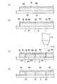
(1)保護部材貼着工程
図9(a)に示すように、ウェーハWの表面W1を粘着テープ等からなる保護部材Pに貼着する。保護部材Pの周縁部には、図2に示したようにリング状に形成されたフレームFが貼着されており、ウェーハWは、保護部材Pを介してフレームFに支持される。このとき、ウェーハWの裏面W2が露出した状態となる。保護部材貼着工程は、少なくとも後述する改質層形成工程の前に行うようにする。2 2nd Embodiment (1) Protection member sticking process As shown to Fig.9 (a), the surface W1 of the wafer W is stuck to the protection member P which consists of adhesive tapes. A frame F formed in a ring shape as shown in FIG. 2 is attached to the peripheral edge of the protective member P, and the wafer W is supported by the frame F via the protective member P. At this time, the back surface W2 of the wafer W is exposed. The protective member attaching step is performed at least before the modified layer forming step described later.
(2)耐エッチングマスク形成工程
次に、図9(a)に示すように、ウェーハWの裏面W2に耐エッチングマスクM1を被覆する。耐エッチングマスクM1としては、例えば、レジスト膜、SiO2(二酸化ケイ素)膜等を使用することができる。耐エッチングマスクM1は、例えば、熱酸化法によって形成することができる。(2) Etching-resistant mask formation process Next, as shown to Fig.9 (a), the back surface W2 of the wafer W is coat | covered with the etching-resistant mask M1. As the etching resistant mask M1, for example, a resist film, a SiO2 (silicon dioxide) film, or the like can be used. The etching resistant mask M1 can be formed by, for example, a thermal oxidation method.
裏面W2全面に耐エッチングマスクM1を被覆した後、図9(b)に示すように、耐エッチングマスクM1のうち、分割予定ラインLの裏面側に対面する部分を除去し、溝G2を形成する。耐エッチングマスクM1がレジスト膜の場合は、例えばフォトマスクを使用し、耐エッチングマスクM1のうち、分割予定ラインLの上方に位置する部分を露光させて除去することができる。また、耐エッチングマスクM1がSiO2膜の場合は、ダイシングによって除去することができる。After covering the entire back surface W2 with the etching resistant mask M1, as shown in FIG. 9B, the portion of the etching resistant mask M1 that faces the back surface side of the division line L is removed to form the groove G2. . When the etching resistant mask M1 is a resist film, for example, a photomask is used, and the portion of the etching resistant mask M1 located above the planned division line L can be exposed and removed. Further, when the etching resistant mask M1 is a SiO2 film, it can be removed by dicing.
さらに、耐エッチングマスクM1に対してレーザー光線を照射することによっても溝G2を形成することができる。この場合の加工条件は、例えば以下のとおりである。
レーザー光線の波長: 355[nm]
平均出力: 1.0[W]
繰り返し周波数: 10[kHz]
スポット径: 20[μm]
送り速度: 100[mm/秒]Furthermore, the groove G2 can also be formed by irradiating the etching resistant mask M1 with a laser beam. The processing conditions in this case are as follows, for example.
Laser beam wavelength: 355 [nm]
Average output: 1.0 [W]
Repetition frequency: 10 [kHz]
Spot diameter: 20 [μm]
Feeding speed: 100 [mm / sec]
(3)改質層形成工程
次に、図9(c)に示すように、ウェーハWに対して透過性を有する波長のレーザー光線31aを照射ヘッド31から照射し、ウェーハWの裏面W2側から溝G2の下方のウェーハWの内部に集光する。そうすると、溝G2は分割予定ラインLに対応してその上方に形成されているため、分割予定ラインLに沿って改質層R2が形成される。レーザー加工の条件は、上記第1の実施形態における改質層形成工程と同様である。(3) Modified Layer Formation Step Next, as shown in FIG. 9C, a
(4)エッチング工程
ウェーハWの内部に改質層R2が形成された後、第1の実施形態と同様に、ドライエッチング又はウェットエッチングによって、改質層R2を侵食させる。そうすると、図9(d)に示すように、改質層R2が除去され、分割予定ラインLに沿って溝G3が形成され、個々のデバイスDに分割される。(4) Etching Step After the modified layer R2 is formed inside the wafer W, the modified layer R2 is eroded by dry etching or wet etching, as in the first embodiment. Then, as shown in FIG. 9D, the modified layer R2 is removed, the groove G3 is formed along the planned division line L, and is divided into individual devices D.
なお、保護部材貼着工程は、耐エッチングマスク形成工程の前、後のいずれに行うようにしてもよい The protective member attaching step may be performed either before or after the etching resistant mask forming step.
3 第3の実施形態
(1)保護部材貼着工程
図10に示すように、ウェーハWの裏面W2を粘着テープ等からなる保護部材Pに貼着する。保護部材Pの周縁部には、リング状に形成されたフレームFが貼着されており、ウェーハWは、保護部材Pを介してフレームFに支持される。このとき、ウェーハWの表面W1が露出した状態となる。表面W1においては、分割予定ラインLによって区画されて複数のデバイスDが形成されている。保護部材貼着工程は、少なくとも後述する改質層形成工程の前に行うようにする。3 3rd Embodiment (1) Protection member sticking process As shown in FIG. 10, the back surface W2 of the wafer W is stuck to the protection member P which consists of adhesive tapes. A frame F formed in a ring shape is attached to the periphery of the protection member P, and the wafer W is supported by the frame F via the protection member P. At this time, the surface W1 of the wafer W is exposed. On the front surface W <b> 1, a plurality of devices D are formed by being partitioned by the division lines L. The protective member attaching step is performed at least before the modified layer forming step described later.
(2)耐エッチングマスク形成工程
図11(a)に示すように、表面W1に耐エッチングマスクM2を被覆する。上記第2の実施形態と同様に、耐エッチングマスクM2としては、例えば、レジスト膜等を使用することができる。(2) Etching-resistant mask formation process As shown in Drawing 11 (a), surface W1 is covered with etching-resistant mask M2. As in the second embodiment, a resist film or the like can be used as the etching resistant mask M2, for example.
次に、図11(b)に示すように、耐エッチングマスクM2のうち、分割予定ラインLに対面する部分を除去し、分割予定ラインLに沿って溝G4を形成する。溝G4の除去方法は、上記第2の実施形態における耐エッチングマスク形成工程と同様である。 Next, as shown in FIG. 11B, the portion of the etching resistant mask M2 that faces the planned division line L is removed, and a groove G4 is formed along the planned division line L. The method for removing the groove G4 is the same as the etching resistant mask forming step in the second embodiment.
(3)改質層形成工程
図11(c)に示すように、ウェーハWに対して透過性を有するレーザー光線31aを照射ヘッド31から照射し、ウェーハWの表面W1側から溝G4の下方のウェーハWの内部に集光する。そうすると、溝G4は分割予定ラインLの上方に形成されているため、分割予定ラインLに沿って改質層R3が形成される。レーザー加工の条件は、上記第1の実施形態と同様である。(3) Modified layer forming step As shown in FIG. 11C, a
(4)エッチング工程
ウェーハWの内部に改質層R3が形成された後、第1の実施形態と同様に、ドライエッチング又はウェットエッチングによって、改質層R3を侵食させる。そうすると、図11(d)及び図12に示すように、改質層R3が除去され、分割予定ラインLに沿って溝G5が形成され、個々のデバイスDに分割される。(4) Etching Step After the modified layer R3 is formed inside the wafer W, the modified layer R3 is eroded by dry etching or wet etching as in the first embodiment. Then, as shown in FIGS. 11D and 12, the modified layer R <b> 3 is removed, a groove G <b> 5 is formed along the planned division line L, and is divided into individual devices D.
以上のように、第1、第2、第3の実施形態のいずれにおいても、ウェーハWの分割予定ラインLに沿ってウェーハWの内部に改質層を形成した後、エッチングによって改質層を侵食させて除去するため、改質層から微粉末が発生することがない。したがって、微粉末がデバイスの表面に付着してデバイスの品質を低下させることがない。また、エッチングによって改質層が除去されるため、改質層の残存に起因するデバイスの抗折強度の低下を防止することができる。 As described above, in any of the first, second, and third embodiments, after the modified layer is formed inside the wafer W along the division line L of the wafer W, the modified layer is formed by etching. Since it is eroded and removed, fine powder is not generated from the modified layer. Therefore, the fine powder does not adhere to the surface of the device and deteriorate the quality of the device. In addition, since the modified layer is removed by etching, it is possible to prevent a decrease in the bending strength of the device due to the remaining of the modified layer.
1:レーザー加工装置
2:保持手段 20:保持面 21:固定部
3:レーザー加工手段
30:基台 31:照射ヘッド
4:加工送り手段
40:ボールネジ 41:ガイドレール 42:モータ 43:スライド部
5:割り出し送り手段
50:ボールネジ 51:ガイドレール 52:モータ 53:基台
6:制御手段
W:ウェーハ
W1:表面 L:分割予定ライン D:デバイス
W2:裏面
P:保護部材 F:フレーム
R1、R2、R3:改質層
G1、G2、G3、G4、G5:溝
M1、M2:耐エッチングマスクDESCRIPTION OF SYMBOLS 1: Laser processing apparatus 2: Holding means 20: Holding surface 21: Fixed part 3: Laser processing means 30: Base 31: Irradiation head 4: Processing feed means 40: Ball screw 41: Guide rail 42: Motor 43: Slide part 5 : Indexing feeding means 50: Ball screw 51: Guide rail 52: Motor 53: Base 6: Control means W: Wafer W 1: Front surface L: Line to be divided D: Device W 2: Back surface P: Protection member F: Frames R 1 and R 2 R3: Modified layers G1, G2, G3, G4, G5: Grooves M1, M2: Etching resistant mask
Claims (3)
Translated fromJapaneseウェーハに対して透過性を有する波長のレーザー光線の集光点を分割予定ラインの内部に位置づけて照射し、該分割予定ラインの内部に該ウェーハの表面側から裏面側に至る改質層を形成する改質層形成工程と、
ウェーハをエッチングするエッチングガスまたはエッチング液を該ウェーハに供給し、該改質層を侵食させて該ウェーハを個々のデバイスに分割するエッチング工程と、
から少なくとも構成され、
該改質層形成工程の前に該ウェーハの表面に保護部材を貼着し、耐エッチングマスクを該ウェーハの裏面に被覆し該分割予定ラインに沿って該耐エッチングマスクを除去して該ウェーハ裏面を露出させる溝を形成する耐エッチングマスク形成工程が含まれる
ウェーハの分割方法。A wafer dividing method in which a plurality of devices are partitioned by lines to be divided and a wafer formed on the surface is divided into individual devices,
A condensing point of a laser beam having a wavelength that is transmissive to the wafer is positioned and irradiated inside the planned division line, and a modified layer extending from the front side to the back side of the wafer is formed inside the planned division line. A modified layer forming step;
Supplying an etching gas or etchant for etching the wafer to erode the modified layer to divide the wafer into individual devices;
At least it consistsof,
Prior to the modified layer forming step, a protective member is attached to the front surface of the wafer, an etching resistant mask is coated on the back surface of the wafer, and the etching resistant mask is removed along the planned dividing line. An etching-resistant mask forming step of forming a groove exposing the waferis included .
ウェーハに対して透過性を有する波長のレーザー光線の集光点を分割予定ラインの内部に位置づけて照射し、該分割予定ラインの内部に該ウェーハの表面側から裏面側に至る改質層を形成する改質層形成工程と、
ウェーハをエッチングするエッチングガスまたはエッチング液を該ウェーハに供給し、該改質層を侵食させて該ウェーハを個々のデバイスに分割するエッチング工程と、
から少なくとも構成され、
該改質層形成工程の前に該ウェーハの裏面に保護部材を貼着し、耐エッチングマスクを該ウェーハの表面に被覆し該分割予定ラインに沿って該耐エッチングマスクを除去して該ウェーハ表面を露出させる溝を形成する耐エッチングマスク形成工程が含まれる
ウェーハの分割方法。A wafer dividing method in which a plurality of devices are partitioned by lines to be divided and a wafer formed on the surface is divided into individual devices,
A condensing point of a laser beam having a wavelength that is transmissive to the wafer is positioned and irradiated inside the planned division line, and a modified layer extending from the front side to the back side of the wafer is formed inside the planned division line. A modified layer forming step;
Supplying an etching gas or etchant for etching the wafer to erode the modified layer to divide the wafer into individual devices;
Consisting of at least
Prior to the modified layer forming step, a protective member is attached to the back surface of the wafer, an etching resistant mask is coated on the surface of the wafer, and the etching resistant mask is removed along the division line. An etching-resistant mask forming step of forming a groove exposing the waferis included .
前記改質層形成工程では、該溝を介してレーザー光線を照射する
請求項1又は2に記載のウェーハの分割方法。In the etching resistant mask forming step, a groove is formed by removing the etching resistant mask along the division line by dicing or laser irradiation,
The wafer dividing method according to claim 1or 2 ,wherein in the modified layer forming step, a laser beam is irradiated through the groove .
Priority Applications (3)
| Application Number | Priority Date | Filing Date | Title |
|---|---|---|---|
| JP2011190647AJP5939752B2 (en) | 2011-09-01 | 2011-09-01 | Wafer dividing method |
| US13/598,147US8673743B2 (en) | 2011-09-01 | 2012-08-29 | Wafer dividing method |
| CN2012103164343ACN102969236A (en) | 2011-09-01 | 2012-08-30 | Wafer dividing method |
Applications Claiming Priority (1)
| Application Number | Priority Date | Filing Date | Title |
|---|---|---|---|
| JP2011190647AJP5939752B2 (en) | 2011-09-01 | 2011-09-01 | Wafer dividing method |
Publications (2)
| Publication Number | Publication Date |
|---|---|
| JP2013055120A JP2013055120A (en) | 2013-03-21 |
| JP5939752B2true JP5939752B2 (en) | 2016-06-22 |
Family
ID=47753474
Family Applications (1)
| Application Number | Title | Priority Date | Filing Date |
|---|---|---|---|
| JP2011190647AActiveJP5939752B2 (en) | 2011-09-01 | 2011-09-01 | Wafer dividing method |
Country Status (3)
| Country | Link |
|---|---|
| US (1) | US8673743B2 (en) |
| JP (1) | JP5939752B2 (en) |
| CN (1) | CN102969236A (en) |
Families Citing this family (27)
| Publication number | Priority date | Publication date | Assignee | Title |
|---|---|---|---|---|
| JP6161496B2 (en)* | 2013-10-01 | 2017-07-12 | 株式会社ディスコ | Photomask manufacturing method |
| JP6235396B2 (en)* | 2014-03-28 | 2017-11-22 | 株式会社ディスコ | Wafer processing method |
| JP6391471B2 (en)* | 2015-01-06 | 2018-09-19 | 株式会社ディスコ | Wafer generation method |
| FI3467565T3 (en)* | 2016-05-27 | 2024-03-19 | Hamamatsu Photonics Kk | Production method for fabry-perot interference filter |
| JP6341959B2 (en) | 2016-05-27 | 2018-06-13 | 浜松ホトニクス株式会社 | Manufacturing method of Fabry-Perot interference filter |
| TWI717519B (en)* | 2016-05-27 | 2021-02-01 | 日商濱松赫德尼古斯股份有限公司 | Manufacturing method of Fabry-Peru interference filter |
| JP6820682B2 (en)* | 2016-07-29 | 2021-01-27 | 株式会社タムラ製作所 | Substrate separation method and semiconductor elements |
| US10724902B2 (en) | 2016-08-24 | 2020-07-28 | Hamamatsu Photonics K.K. | Fabry-Perot interference filter |
| JP6821245B2 (en)* | 2016-10-11 | 2021-01-27 | 株式会社ディスコ | Wafer processing method |
| DE102016224978B4 (en)* | 2016-12-14 | 2022-12-29 | Disco Corporation | substrate processing method |
| DE102017200631B4 (en) | 2017-01-17 | 2022-12-29 | Disco Corporation | Method of processing a substrate |
| CN108630599A (en)* | 2017-03-22 | 2018-10-09 | 东莞新科技术研究开发有限公司 | The forming method of chip |
| JP7063543B2 (en)* | 2017-04-17 | 2022-05-09 | 浜松ホトニクス株式会社 | How to cut the object to be machined |
| JP2018182141A (en)* | 2017-04-17 | 2018-11-15 | 浜松ホトニクス株式会社 | Workpiece cutting method |
| JP7063542B2 (en) | 2017-04-17 | 2022-05-09 | 浜松ホトニクス株式会社 | How to cut the object to be machined |
| JP2018182138A (en)* | 2017-04-17 | 2018-11-15 | 浜松ホトニクス株式会社 | Workpiece cutting method |
| JP6957185B2 (en)* | 2017-04-17 | 2021-11-02 | 浜松ホトニクス株式会社 | Processing object cutting method and semiconductor chip |
| JP7098284B2 (en) | 2017-07-06 | 2022-07-11 | 株式会社ディスコ | Laser processing equipment and laser processing method |
| JP6925900B2 (en)* | 2017-07-20 | 2021-08-25 | 岩谷産業株式会社 | Cutting method |
| JP6957252B2 (en) | 2017-07-20 | 2021-11-02 | 岩谷産業株式会社 | Cutting method |
| DE102017212858B4 (en) | 2017-07-26 | 2024-08-29 | Disco Corporation | Method for processing a substrate |
| JP6985060B2 (en)* | 2017-08-17 | 2021-12-22 | 株式会社ディスコ | Wafer processing method |
| JP2019079884A (en) | 2017-10-23 | 2019-05-23 | 株式会社ディスコ | Wafer processing method |
| US10818551B2 (en)* | 2019-01-09 | 2020-10-27 | Semiconductor Components Industries, Llc | Plasma die singulation systems and related methods |
| JP7446673B2 (en)* | 2020-02-21 | 2024-03-11 | 株式会社ディスコ | Wafer processing method |
| DE102020204910A1 (en)* | 2020-04-17 | 2021-10-21 | Robert Bosch Gesellschaft mit beschränkter Haftung | A method of making at least first and second micromirror devices |
| JP2023179101A (en)* | 2022-06-07 | 2023-12-19 | 日本電気硝子株式会社 | Glass sheet and manufacturing method thereof |
Family Cites Families (20)
| Publication number | Priority date | Publication date | Assignee | Title |
|---|---|---|---|---|
| JPH097975A (en)* | 1995-06-22 | 1997-01-10 | Hitachi Ltd | Semiconductor device and manufacturing method thereof |
| JP3408805B2 (en) | 2000-09-13 | 2003-05-19 | 浜松ホトニクス株式会社 | Cutting origin region forming method and workpiece cutting method |
| JP4659300B2 (en)* | 2000-09-13 | 2011-03-30 | 浜松ホトニクス株式会社 | Laser processing method and semiconductor chip manufacturing method |
| JP4018096B2 (en)* | 2004-10-05 | 2007-12-05 | 松下電器産業株式会社 | Semiconductor wafer dividing method and semiconductor element manufacturing method |
| JP4809632B2 (en)* | 2005-06-01 | 2011-11-09 | ルネサスエレクトロニクス株式会社 | Manufacturing method of semiconductor device |
| JP2007134454A (en)* | 2005-11-09 | 2007-05-31 | Toshiba Corp | Manufacturing method of semiconductor device |
| JP4372115B2 (en)* | 2006-05-12 | 2009-11-25 | パナソニック株式会社 | Semiconductor device manufacturing method and semiconductor module manufacturing method |
| JP5197586B2 (en)* | 2007-05-25 | 2013-05-15 | 浜松ホトニクス株式会社 | Cutting method |
| JP2009200140A (en)* | 2008-02-20 | 2009-09-03 | Disco Abrasive Syst Ltd | Method of manufacturing semiconductor chip |
| US7859084B2 (en)* | 2008-02-28 | 2010-12-28 | Panasonic Corporation | Semiconductor substrate |
| JP2009206291A (en)* | 2008-02-28 | 2009-09-10 | Panasonic Corp | Semiconductor substrate, semiconductor device, and manufacturing method thereof |
| JP2009290148A (en)* | 2008-06-02 | 2009-12-10 | Disco Abrasive Syst Ltd | Method of dividing wafer |
| JP2010016116A (en)* | 2008-07-02 | 2010-01-21 | Disco Abrasive Syst Ltd | Method of manufacturing semiconductor device |
| JP2010050175A (en)* | 2008-08-20 | 2010-03-04 | Disco Abrasive Syst Ltd | Laser processing method and laser processing device |
| US20120234807A1 (en)* | 2009-12-07 | 2012-09-20 | J.P. Sercel Associates Inc. | Laser scribing with extended depth affectation into a workplace |
| JP2011165766A (en)* | 2010-02-05 | 2011-08-25 | Disco Abrasive Syst Ltd | Method of processing optical device wafer |
| JP2011224931A (en)* | 2010-04-22 | 2011-11-10 | Disco Corp | Optical device wafer processing method and laser processing apparatus |
| JP5645593B2 (en)* | 2010-10-21 | 2014-12-24 | 株式会社ディスコ | Wafer division method |
| JP5904720B2 (en)* | 2011-05-12 | 2016-04-20 | 株式会社ディスコ | Wafer division method |
| JP5860228B2 (en)* | 2011-06-13 | 2016-02-16 | 株式会社ディスコ | Laser processing equipment |
- 2011
- 2011-09-01JPJP2011190647Apatent/JP5939752B2/enactiveActive
- 2012
- 2012-08-29USUS13/598,147patent/US8673743B2/enactiveActive
- 2012-08-30CNCN2012103164343Apatent/CN102969236A/enactivePending
Also Published As
| Publication number | Publication date |
|---|---|
| CN102969236A (en) | 2013-03-13 |
| US20130059428A1 (en) | 2013-03-07 |
| US8673743B2 (en) | 2014-03-18 |
| JP2013055120A (en) | 2013-03-21 |
Similar Documents
| Publication | Publication Date | Title |
|---|---|---|
| JP5939752B2 (en) | Wafer dividing method | |
| JP5162163B2 (en) | Wafer laser processing method | |
| JP6532273B2 (en) | Wafer processing method | |
| JP6162018B2 (en) | Wafer processing method | |
| JP6178077B2 (en) | Wafer processing method | |
| TWI411487B (en) | Laser processing of gallium arsenide wafers | |
| JP2005129607A (en) | Wafer division method | |
| JP2018037432A (en) | Wafer production method | |
| JP2017041482A (en) | Wafer processing method | |
| JP2005135964A (en) | Wafer division method | |
| JP2011161491A (en) | Laser beam machining apparatus | |
| JP2016076671A (en) | Wafer processing method | |
| CN105304563A (en) | Processing method of package substrate | |
| JP2004179302A (en) | Method of dividing semiconductor wafer | |
| JP2015056489A (en) | Wafer processing method | |
| JP5536344B2 (en) | Laser processing equipment | |
| JP6692578B2 (en) | Wafer processing method | |
| KR102527033B1 (en) | Wafer processing method | |
| JP6521711B2 (en) | Wafer processing method | |
| JP2018067647A (en) | Wafer processing method | |
| JP6068074B2 (en) | Method for forming gettering layer | |
| JP2013102039A (en) | Semiconductor wafer processing method | |
| JP2012160515A (en) | Workpiece processing method | |
| JP2016162809A (en) | Wafer processing method | |
| JP5912283B2 (en) | Processing method of adhesive tape and wafer |
Legal Events
| Date | Code | Title | Description |
|---|---|---|---|
| A621 | Written request for application examination | Free format text:JAPANESE INTERMEDIATE CODE: A621 Effective date:20140825 | |
| RD02 | Notification of acceptance of power of attorney | Free format text:JAPANESE INTERMEDIATE CODE: A7422 Effective date:20150427 | |
| A977 | Report on retrieval | Free format text:JAPANESE INTERMEDIATE CODE: A971007 Effective date:20150820 | |
| A131 | Notification of reasons for refusal | Free format text:JAPANESE INTERMEDIATE CODE: A131 Effective date:20150929 | |
| A521 | Request for written amendment filed | Free format text:JAPANESE INTERMEDIATE CODE: A523 Effective date:20151127 | |
| TRDD | Decision of grant or rejection written | ||
| A01 | Written decision to grant a patent or to grant a registration (utility model) | Free format text:JAPANESE INTERMEDIATE CODE: A01 Effective date:20160421 | |
| A61 | First payment of annual fees (during grant procedure) | Free format text:JAPANESE INTERMEDIATE CODE: A61 Effective date:20160517 | |
| R150 | Certificate of patent or registration of utility model | Ref document number:5939752 Country of ref document:JP Free format text:JAPANESE INTERMEDIATE CODE: R150 | |
| R250 | Receipt of annual fees | Free format text:JAPANESE INTERMEDIATE CODE: R250 | |
| R250 | Receipt of annual fees | Free format text:JAPANESE INTERMEDIATE CODE: R250 | |
| R250 | Receipt of annual fees | Free format text:JAPANESE INTERMEDIATE CODE: R250 | |
| R250 | Receipt of annual fees | Free format text:JAPANESE INTERMEDIATE CODE: R250 | |
| R250 | Receipt of annual fees | Free format text:JAPANESE INTERMEDIATE CODE: R250 | |
| R250 | Receipt of annual fees | Free format text:JAPANESE INTERMEDIATE CODE: R250 | |
| R250 | Receipt of annual fees | Free format text:JAPANESE INTERMEDIATE CODE: R250 |