JP5939184B2 - Manufacturing method of semiconductor device - Google Patents
Manufacturing method of semiconductor deviceDownload PDFInfo
- Publication number
- JP5939184B2 JP5939184B2JP2013060691AJP2013060691AJP5939184B2JP 5939184 B2JP5939184 B2JP 5939184B2JP 2013060691 AJP2013060691 AJP 2013060691AJP 2013060691 AJP2013060691 AJP 2013060691AJP 5939184 B2JP5939184 B2JP 5939184B2
- Authority
- JP
- Japan
- Prior art keywords
- substrate
- film
- thin film
- insulating thin
- electrode
- Prior art date
- Legal status (The legal status is an assumption and is not a legal conclusion. Google has not performed a legal analysis and makes no representation as to the accuracy of the status listed.)
- Active
Links
- 239000004065semiconductorSubstances0.000titleclaimsdescription87
- 238000004519manufacturing processMethods0.000titleclaimsdescription38
- 239000000758substrateSubstances0.000claimsdescription185
- 239000010408filmSubstances0.000claimsdescription141
- 239000010409thin filmSubstances0.000claimsdescription98
- 238000000034methodMethods0.000claimsdescription80
- 230000008569processEffects0.000claimsdescription29
- 238000000231atomic layer depositionMethods0.000claimsdescription23
- 239000002184metalSubstances0.000claimsdescription20
- 229910052751metalInorganic materials0.000claimsdescription20
- 239000000463materialSubstances0.000claimsdescription14
- 239000013078crystalSubstances0.000claimsdescription10
- 238000000151depositionMethods0.000claimsdescription6
- 239000010410layerSubstances0.000description100
- 239000010949copperSubstances0.000description62
- RYGMFSIKBFXOCR-UHFFFAOYSA-NCopperChemical compound[Cu]RYGMFSIKBFXOCR-UHFFFAOYSA-N0.000description27
- 229910052802copperInorganic materials0.000description27
- 230000015572biosynthetic processEffects0.000description24
- 238000003384imaging methodMethods0.000description23
- 239000000376reactantSubstances0.000description21
- 238000006243chemical reactionMethods0.000description18
- 230000004888barrier functionEffects0.000description17
- 238000010438heat treatmentMethods0.000description17
- BOTDANWDWHJENH-UHFFFAOYSA-NTetraethyl orthosilicateChemical compoundCCO[Si](OCC)(OCC)OCCBOTDANWDWHJENH-UHFFFAOYSA-N0.000description15
- 239000007789gasSubstances0.000description13
- 239000012535impuritySubstances0.000description11
- 238000009792diffusion processMethods0.000description8
- 239000011229interlayerSubstances0.000description8
- 230000001681protective effectEffects0.000description7
- VYPSYNLAJGMNEJ-UHFFFAOYSA-NSilicium dioxideChemical groupO=[Si]=OVYPSYNLAJGMNEJ-UHFFFAOYSA-N0.000description6
- 150000004767nitridesChemical class0.000description6
- 230000003287optical effectEffects0.000description6
- 229910052814silicon oxideInorganic materials0.000description6
- 229910052581Si3N4Inorganic materials0.000description5
- 229910004298SiO 2Inorganic materials0.000description5
- 238000010586diagramMethods0.000description5
- HQVNEWCFYHHQES-UHFFFAOYSA-Nsilicon nitrideChemical compoundN12[Si]34N5[Si]62N3[Si]51N64HQVNEWCFYHHQES-UHFFFAOYSA-N0.000description5
- XLYOFNOQVPJJNP-UHFFFAOYSA-NwaterChemical compoundOXLYOFNOQVPJJNP-UHFFFAOYSA-N0.000description5
- 238000005229chemical vapour depositionMethods0.000description4
- 230000008021depositionEffects0.000description4
- 229910021421monocrystalline siliconInorganic materials0.000description4
- 238000001179sorption measurementMethods0.000description4
- 239000002344surface layerSubstances0.000description4
- 230000000694effectsEffects0.000description3
- 230000006870functionEffects0.000description3
- 238000002360preparation methodMethods0.000description3
- CBENFWSGALASAD-UHFFFAOYSA-NOzoneChemical compound[O-][O+]=OCBENFWSGALASAD-UHFFFAOYSA-N0.000description2
- 238000009833condensationMethods0.000description2
- 230000005494condensationEffects0.000description2
- 239000000470constituentSubstances0.000description2
- 238000007872degassingMethods0.000description2
- 230000018044dehydrationEffects0.000description2
- 238000006297dehydration reactionMethods0.000description2
- 230000002542deteriorative effectEffects0.000description2
- CJNBYAVZURUTKZ-UHFFFAOYSA-Nhafnium(iv) oxideChemical compoundO=[Hf]=OCJNBYAVZURUTKZ-UHFFFAOYSA-N0.000description2
- 230000002093peripheral effectEffects0.000description2
- 238000003860storageMethods0.000description2
- 239000000126substanceSubstances0.000description2
- 239000011800void materialSubstances0.000description2
- QGZKDVFQNNGYKY-UHFFFAOYSA-NAmmoniaChemical compoundNQGZKDVFQNNGYKY-UHFFFAOYSA-N0.000description1
- IJGRMHOSHXDMSA-UHFFFAOYSA-NAtomic nitrogenChemical compoundN#NIJGRMHOSHXDMSA-UHFFFAOYSA-N0.000description1
- BLRPTPMANUNPDV-UHFFFAOYSA-NSilaneChemical compound[SiH4]BLRPTPMANUNPDV-UHFFFAOYSA-N0.000description1
- XUIMIQQOPSSXEZ-UHFFFAOYSA-NSiliconChemical compound[Si]XUIMIQQOPSSXEZ-UHFFFAOYSA-N0.000description1
- 239000003990capacitorSubstances0.000description1
- 238000000576coating methodMethods0.000description1
- 239000003086colorantSubstances0.000description1
- 239000012141concentrateSubstances0.000description1
- 239000004020conductorSubstances0.000description1
- MROCJMGDEKINLD-UHFFFAOYSA-NdichlorosilaneChemical compoundCl[SiH2]ClMROCJMGDEKINLD-UHFFFAOYSA-N0.000description1
- 229910001873dinitrogenInorganic materials0.000description1
- -1for exampleSubstances0.000description1
- 125000002887hydroxy groupChemical group[H]O*0.000description1
- 230000006872improvementEffects0.000description1
- 239000011261inert gasSubstances0.000description1
- 238000005304joiningMethods0.000description1
- 239000012528membraneSubstances0.000description1
- 239000000203mixtureSubstances0.000description1
- 238000002161passivationMethods0.000description1
- 238000005498polishingMethods0.000description1
- 238000007781pre-processingMethods0.000description1
- 230000002265preventionEffects0.000description1
- 230000001737promoting effectEffects0.000description1
- 238000010926purgeMethods0.000description1
- 229910000077silaneInorganic materials0.000description1
- 229910052710siliconInorganic materials0.000description1
- 239000010703siliconSubstances0.000description1
- 239000002356single layerSubstances0.000description1
- 238000000427thin-film depositionMethods0.000description1
Images


Classifications
- H—ELECTRICITY
- H01—ELECTRIC ELEMENTS
- H01L—SEMICONDUCTOR DEVICES NOT COVERED BY CLASS H10
- H01L21/00—Processes or apparatus adapted for the manufacture or treatment of semiconductor or solid state devices or of parts thereof
- H01L21/02—Manufacture or treatment of semiconductor devices or of parts thereof
- H01L21/04—Manufacture or treatment of semiconductor devices or of parts thereof the devices having potential barriers, e.g. a PN junction, depletion layer or carrier concentration layer
- H01L21/18—Manufacture or treatment of semiconductor devices or of parts thereof the devices having potential barriers, e.g. a PN junction, depletion layer or carrier concentration layer the devices having semiconductor bodies comprising elements of Group IV of the Periodic Table or AIIIBV compounds with or without impurities, e.g. doping materials
- H01L21/20—Deposition of semiconductor materials on a substrate, e.g. epitaxial growth solid phase epitaxy
- H01L21/2003—Deposition of semiconductor materials on a substrate, e.g. epitaxial growth solid phase epitaxy characterised by the substrate
- H01L21/2007—Bonding of semiconductor wafers to insulating substrates or to semiconducting substrates using an intermediate insulating layer
- H—ELECTRICITY
- H01—ELECTRIC ELEMENTS
- H01L—SEMICONDUCTOR DEVICES NOT COVERED BY CLASS H10
- H01L21/00—Processes or apparatus adapted for the manufacture or treatment of semiconductor or solid state devices or of parts thereof
- H01L21/70—Manufacture or treatment of devices consisting of a plurality of solid state components formed in or on a common substrate or of parts thereof; Manufacture of integrated circuit devices or of parts thereof
- H01L21/71—Manufacture of specific parts of devices defined in group H01L21/70
- H01L21/768—Applying interconnections to be used for carrying current between separate components within a device comprising conductors and dielectrics
- H01L21/76801—Applying interconnections to be used for carrying current between separate components within a device comprising conductors and dielectrics characterised by the formation and the after-treatment of the dielectrics, e.g. smoothing
- H01L21/76822—Modification of the material of dielectric layers, e.g. grading, after-treatment to improve the stability of the layers, to increase their density etc.
- H01L21/76823—Modification of the material of dielectric layers, e.g. grading, after-treatment to improve the stability of the layers, to increase their density etc. transforming an insulating layer into a conductive layer
- H—ELECTRICITY
- H01—ELECTRIC ELEMENTS
- H01L—SEMICONDUCTOR DEVICES NOT COVERED BY CLASS H10
- H01L21/00—Processes or apparatus adapted for the manufacture or treatment of semiconductor or solid state devices or of parts thereof
- H01L21/70—Manufacture or treatment of devices consisting of a plurality of solid state components formed in or on a common substrate or of parts thereof; Manufacture of integrated circuit devices or of parts thereof
- H01L21/71—Manufacture of specific parts of devices defined in group H01L21/70
- H01L21/768—Applying interconnections to be used for carrying current between separate components within a device comprising conductors and dielectrics
- H01L21/76801—Applying interconnections to be used for carrying current between separate components within a device comprising conductors and dielectrics characterised by the formation and the after-treatment of the dielectrics, e.g. smoothing
- H01L21/76822—Modification of the material of dielectric layers, e.g. grading, after-treatment to improve the stability of the layers, to increase their density etc.
- H01L21/76828—Modification of the material of dielectric layers, e.g. grading, after-treatment to improve the stability of the layers, to increase their density etc. thermal treatment
- H—ELECTRICITY
- H01—ELECTRIC ELEMENTS
- H01L—SEMICONDUCTOR DEVICES NOT COVERED BY CLASS H10
- H01L21/00—Processes or apparatus adapted for the manufacture or treatment of semiconductor or solid state devices or of parts thereof
- H01L21/70—Manufacture or treatment of devices consisting of a plurality of solid state components formed in or on a common substrate or of parts thereof; Manufacture of integrated circuit devices or of parts thereof
- H01L21/71—Manufacture of specific parts of devices defined in group H01L21/70
- H01L21/768—Applying interconnections to be used for carrying current between separate components within a device comprising conductors and dielectrics
- H01L21/76838—Applying interconnections to be used for carrying current between separate components within a device comprising conductors and dielectrics characterised by the formation and the after-treatment of the conductors
- H01L21/76841—Barrier, adhesion or liner layers
- H01L21/76853—Barrier, adhesion or liner layers characterized by particular after-treatment steps
- H01L21/76861—Post-treatment or after-treatment not introducing additional chemical elements into the layer
- H01L21/76864—Thermal treatment
- H—ELECTRICITY
- H01—ELECTRIC ELEMENTS
- H01L—SEMICONDUCTOR DEVICES NOT COVERED BY CLASS H10
- H01L24/00—Arrangements for connecting or disconnecting semiconductor or solid-state bodies; Methods or apparatus related thereto
- H01L24/01—Means for bonding being attached to, or being formed on, the surface to be connected, e.g. chip-to-package, die-attach, "first-level" interconnects; Manufacturing methods related thereto
- H01L24/02—Bonding areas ; Manufacturing methods related thereto
- H01L24/04—Structure, shape, material or disposition of the bonding areas prior to the connecting process
- H01L24/05—Structure, shape, material or disposition of the bonding areas prior to the connecting process of an individual bonding area
- H—ELECTRICITY
- H01—ELECTRIC ELEMENTS
- H01L—SEMICONDUCTOR DEVICES NOT COVERED BY CLASS H10
- H01L24/00—Arrangements for connecting or disconnecting semiconductor or solid-state bodies; Methods or apparatus related thereto
- H01L24/01—Means for bonding being attached to, or being formed on, the surface to be connected, e.g. chip-to-package, die-attach, "first-level" interconnects; Manufacturing methods related thereto
- H01L24/02—Bonding areas ; Manufacturing methods related thereto
- H01L24/07—Structure, shape, material or disposition of the bonding areas after the connecting process
- H01L24/08—Structure, shape, material or disposition of the bonding areas after the connecting process of an individual bonding area
- H—ELECTRICITY
- H01—ELECTRIC ELEMENTS
- H01L—SEMICONDUCTOR DEVICES NOT COVERED BY CLASS H10
- H01L24/00—Arrangements for connecting or disconnecting semiconductor or solid-state bodies; Methods or apparatus related thereto
- H01L24/80—Methods for connecting semiconductor or other solid state bodies using means for bonding being attached to, or being formed on, the surface to be connected
- H—ELECTRICITY
- H04—ELECTRIC COMMUNICATION TECHNIQUE
- H04N—PICTORIAL COMMUNICATION, e.g. TELEVISION
- H04N23/00—Cameras or camera modules comprising electronic image sensors; Control thereof
- H04N23/50—Constructional details
- H04N23/55—Optical parts specially adapted for electronic image sensors; Mounting thereof
- H—ELECTRICITY
- H10—SEMICONDUCTOR DEVICES; ELECTRIC SOLID-STATE DEVICES NOT OTHERWISE PROVIDED FOR
- H10F—INORGANIC SEMICONDUCTOR DEVICES SENSITIVE TO INFRARED RADIATION, LIGHT, ELECTROMAGNETIC RADIATION OF SHORTER WAVELENGTH OR CORPUSCULAR RADIATION
- H10F39/00—Integrated devices, or assemblies of multiple devices, comprising at least one element covered by group H10F30/00, e.g. radiation detectors comprising photodiode arrays
- H10F39/011—Manufacture or treatment of image sensors covered by group H10F39/12
- H10F39/014—Manufacture or treatment of image sensors covered by group H10F39/12 of CMOS image sensors
- H—ELECTRICITY
- H10—SEMICONDUCTOR DEVICES; ELECTRIC SOLID-STATE DEVICES NOT OTHERWISE PROVIDED FOR
- H10F—INORGANIC SEMICONDUCTOR DEVICES SENSITIVE TO INFRARED RADIATION, LIGHT, ELECTROMAGNETIC RADIATION OF SHORTER WAVELENGTH OR CORPUSCULAR RADIATION
- H10F39/00—Integrated devices, or assemblies of multiple devices, comprising at least one element covered by group H10F30/00, e.g. radiation detectors comprising photodiode arrays
- H10F39/011—Manufacture or treatment of image sensors covered by group H10F39/12
- H10F39/018—Manufacture or treatment of image sensors covered by group H10F39/12 of hybrid image sensors
- H—ELECTRICITY
- H10—SEMICONDUCTOR DEVICES; ELECTRIC SOLID-STATE DEVICES NOT OTHERWISE PROVIDED FOR
- H10F—INORGANIC SEMICONDUCTOR DEVICES SENSITIVE TO INFRARED RADIATION, LIGHT, ELECTROMAGNETIC RADIATION OF SHORTER WAVELENGTH OR CORPUSCULAR RADIATION
- H10F39/00—Integrated devices, or assemblies of multiple devices, comprising at least one element covered by group H10F30/00, e.g. radiation detectors comprising photodiode arrays
- H10F39/10—Integrated devices
- H10F39/12—Image sensors
- H10F39/18—Complementary metal-oxide-semiconductor [CMOS] image sensors; Photodiode array image sensors
- H—ELECTRICITY
- H10—SEMICONDUCTOR DEVICES; ELECTRIC SOLID-STATE DEVICES NOT OTHERWISE PROVIDED FOR
- H10F—INORGANIC SEMICONDUCTOR DEVICES SENSITIVE TO INFRARED RADIATION, LIGHT, ELECTROMAGNETIC RADIATION OF SHORTER WAVELENGTH OR CORPUSCULAR RADIATION
- H10F39/00—Integrated devices, or assemblies of multiple devices, comprising at least one element covered by group H10F30/00, e.g. radiation detectors comprising photodiode arrays
- H10F39/10—Integrated devices
- H10F39/12—Image sensors
- H10F39/199—Back-illuminated image sensors
- H—ELECTRICITY
- H10—SEMICONDUCTOR DEVICES; ELECTRIC SOLID-STATE DEVICES NOT OTHERWISE PROVIDED FOR
- H10F—INORGANIC SEMICONDUCTOR DEVICES SENSITIVE TO INFRARED RADIATION, LIGHT, ELECTROMAGNETIC RADIATION OF SHORTER WAVELENGTH OR CORPUSCULAR RADIATION
- H10F39/00—Integrated devices, or assemblies of multiple devices, comprising at least one element covered by group H10F30/00, e.g. radiation detectors comprising photodiode arrays
- H10F39/80—Constructional details of image sensors
- H10F39/803—Pixels having integrated switching, control, storage or amplification elements
- H10F39/8037—Pixels having integrated switching, control, storage or amplification elements the integrated elements comprising a transistor
- H—ELECTRICITY
- H10—SEMICONDUCTOR DEVICES; ELECTRIC SOLID-STATE DEVICES NOT OTHERWISE PROVIDED FOR
- H10F—INORGANIC SEMICONDUCTOR DEVICES SENSITIVE TO INFRARED RADIATION, LIGHT, ELECTROMAGNETIC RADIATION OF SHORTER WAVELENGTH OR CORPUSCULAR RADIATION
- H10F39/00—Integrated devices, or assemblies of multiple devices, comprising at least one element covered by group H10F30/00, e.g. radiation detectors comprising photodiode arrays
- H10F39/80—Constructional details of image sensors
- H10F39/804—Containers or encapsulations
- H—ELECTRICITY
- H10—SEMICONDUCTOR DEVICES; ELECTRIC SOLID-STATE DEVICES NOT OTHERWISE PROVIDED FOR
- H10F—INORGANIC SEMICONDUCTOR DEVICES SENSITIVE TO INFRARED RADIATION, LIGHT, ELECTROMAGNETIC RADIATION OF SHORTER WAVELENGTH OR CORPUSCULAR RADIATION
- H10F39/00—Integrated devices, or assemblies of multiple devices, comprising at least one element covered by group H10F30/00, e.g. radiation detectors comprising photodiode arrays
- H10F39/80—Constructional details of image sensors
- H10F39/805—Coatings
- H10F39/8053—Colour filters
- H—ELECTRICITY
- H10—SEMICONDUCTOR DEVICES; ELECTRIC SOLID-STATE DEVICES NOT OTHERWISE PROVIDED FOR
- H10F—INORGANIC SEMICONDUCTOR DEVICES SENSITIVE TO INFRARED RADIATION, LIGHT, ELECTROMAGNETIC RADIATION OF SHORTER WAVELENGTH OR CORPUSCULAR RADIATION
- H10F39/00—Integrated devices, or assemblies of multiple devices, comprising at least one element covered by group H10F30/00, e.g. radiation detectors comprising photodiode arrays
- H10F39/80—Constructional details of image sensors
- H10F39/805—Coatings
- H10F39/8057—Optical shielding
- H—ELECTRICITY
- H10—SEMICONDUCTOR DEVICES; ELECTRIC SOLID-STATE DEVICES NOT OTHERWISE PROVIDED FOR
- H10F—INORGANIC SEMICONDUCTOR DEVICES SENSITIVE TO INFRARED RADIATION, LIGHT, ELECTROMAGNETIC RADIATION OF SHORTER WAVELENGTH OR CORPUSCULAR RADIATION
- H10F39/00—Integrated devices, or assemblies of multiple devices, comprising at least one element covered by group H10F30/00, e.g. radiation detectors comprising photodiode arrays
- H10F39/80—Constructional details of image sensors
- H10F39/806—Optical elements or arrangements associated with the image sensors
- H10F39/8063—Microlenses
- H—ELECTRICITY
- H10—SEMICONDUCTOR DEVICES; ELECTRIC SOLID-STATE DEVICES NOT OTHERWISE PROVIDED FOR
- H10F—INORGANIC SEMICONDUCTOR DEVICES SENSITIVE TO INFRARED RADIATION, LIGHT, ELECTROMAGNETIC RADIATION OF SHORTER WAVELENGTH OR CORPUSCULAR RADIATION
- H10F39/00—Integrated devices, or assemblies of multiple devices, comprising at least one element covered by group H10F30/00, e.g. radiation detectors comprising photodiode arrays
- H10F39/80—Constructional details of image sensors
- H10F39/809—Constructional details of image sensors of hybrid image sensors
- H—ELECTRICITY
- H10—SEMICONDUCTOR DEVICES; ELECTRIC SOLID-STATE DEVICES NOT OTHERWISE PROVIDED FOR
- H10F—INORGANIC SEMICONDUCTOR DEVICES SENSITIVE TO INFRARED RADIATION, LIGHT, ELECTROMAGNETIC RADIATION OF SHORTER WAVELENGTH OR CORPUSCULAR RADIATION
- H10F39/00—Integrated devices, or assemblies of multiple devices, comprising at least one element covered by group H10F30/00, e.g. radiation detectors comprising photodiode arrays
- H10F39/80—Constructional details of image sensors
- H10F39/811—Interconnections
- H—ELECTRICITY
- H01—ELECTRIC ELEMENTS
- H01L—SEMICONDUCTOR DEVICES NOT COVERED BY CLASS H10
- H01L2224/00—Indexing scheme for arrangements for connecting or disconnecting semiconductor or solid-state bodies and methods related thereto as covered by H01L24/00
- H01L2224/01—Means for bonding being attached to, or being formed on, the surface to be connected, e.g. chip-to-package, die-attach, "first-level" interconnects; Manufacturing methods related thereto
- H01L2224/02—Bonding areas; Manufacturing methods related thereto
- H01L2224/04—Structure, shape, material or disposition of the bonding areas prior to the connecting process
- H01L2224/05—Structure, shape, material or disposition of the bonding areas prior to the connecting process of an individual bonding area
- H01L2224/05001—Internal layers
- H01L2224/05099—Material
- H01L2224/051—Material with a principal constituent of the material being a metal or a metalloid, e.g. boron [B], silicon [Si], germanium [Ge], arsenic [As], antimony [Sb], tellurium [Te] and polonium [Po], and alloys thereof
- H01L2224/05138—Material with a principal constituent of the material being a metal or a metalloid, e.g. boron [B], silicon [Si], germanium [Ge], arsenic [As], antimony [Sb], tellurium [Te] and polonium [Po], and alloys thereof the principal constituent melting at a temperature of greater than or equal to 950°C and less than 1550°C
- H01L2224/05147—Copper [Cu] as principal constituent
- H—ELECTRICITY
- H01—ELECTRIC ELEMENTS
- H01L—SEMICONDUCTOR DEVICES NOT COVERED BY CLASS H10
- H01L2224/00—Indexing scheme for arrangements for connecting or disconnecting semiconductor or solid-state bodies and methods related thereto as covered by H01L24/00
- H01L2224/01—Means for bonding being attached to, or being formed on, the surface to be connected, e.g. chip-to-package, die-attach, "first-level" interconnects; Manufacturing methods related thereto
- H01L2224/02—Bonding areas; Manufacturing methods related thereto
- H01L2224/04—Structure, shape, material or disposition of the bonding areas prior to the connecting process
- H01L2224/05—Structure, shape, material or disposition of the bonding areas prior to the connecting process of an individual bonding area
- H01L2224/0554—External layer
- H01L2224/05541—Structure
- H01L2224/05547—Structure comprising a core and a coating
- H—ELECTRICITY
- H01—ELECTRIC ELEMENTS
- H01L—SEMICONDUCTOR DEVICES NOT COVERED BY CLASS H10
- H01L2224/00—Indexing scheme for arrangements for connecting or disconnecting semiconductor or solid-state bodies and methods related thereto as covered by H01L24/00
- H01L2224/01—Means for bonding being attached to, or being formed on, the surface to be connected, e.g. chip-to-package, die-attach, "first-level" interconnects; Manufacturing methods related thereto
- H01L2224/02—Bonding areas; Manufacturing methods related thereto
- H01L2224/04—Structure, shape, material or disposition of the bonding areas prior to the connecting process
- H01L2224/05—Structure, shape, material or disposition of the bonding areas prior to the connecting process of an individual bonding area
- H01L2224/0554—External layer
- H01L2224/05573—Single external layer
- H—ELECTRICITY
- H01—ELECTRIC ELEMENTS
- H01L—SEMICONDUCTOR DEVICES NOT COVERED BY CLASS H10
- H01L2224/00—Indexing scheme for arrangements for connecting or disconnecting semiconductor or solid-state bodies and methods related thereto as covered by H01L24/00
- H01L2224/01—Means for bonding being attached to, or being formed on, the surface to be connected, e.g. chip-to-package, die-attach, "first-level" interconnects; Manufacturing methods related thereto
- H01L2224/02—Bonding areas; Manufacturing methods related thereto
- H01L2224/04—Structure, shape, material or disposition of the bonding areas prior to the connecting process
- H01L2224/05—Structure, shape, material or disposition of the bonding areas prior to the connecting process of an individual bonding area
- H01L2224/0554—External layer
- H01L2224/05599—Material
- H01L2224/05686—Material with a principal constituent of the material being a non metallic, non metalloid inorganic material
- H—ELECTRICITY
- H01—ELECTRIC ELEMENTS
- H01L—SEMICONDUCTOR DEVICES NOT COVERED BY CLASS H10
- H01L2224/00—Indexing scheme for arrangements for connecting or disconnecting semiconductor or solid-state bodies and methods related thereto as covered by H01L24/00
- H01L2224/01—Means for bonding being attached to, or being formed on, the surface to be connected, e.g. chip-to-package, die-attach, "first-level" interconnects; Manufacturing methods related thereto
- H01L2224/02—Bonding areas; Manufacturing methods related thereto
- H01L2224/07—Structure, shape, material or disposition of the bonding areas after the connecting process
- H01L2224/08—Structure, shape, material or disposition of the bonding areas after the connecting process of an individual bonding area
- H01L2224/0805—Shape
- H01L2224/08057—Shape in side view
- H01L2224/08058—Shape in side view being non uniform along the bonding area
- H—ELECTRICITY
- H01—ELECTRIC ELEMENTS
- H01L—SEMICONDUCTOR DEVICES NOT COVERED BY CLASS H10
- H01L2224/00—Indexing scheme for arrangements for connecting or disconnecting semiconductor or solid-state bodies and methods related thereto as covered by H01L24/00
- H01L2224/01—Means for bonding being attached to, or being formed on, the surface to be connected, e.g. chip-to-package, die-attach, "first-level" interconnects; Manufacturing methods related thereto
- H01L2224/02—Bonding areas; Manufacturing methods related thereto
- H01L2224/07—Structure, shape, material or disposition of the bonding areas after the connecting process
- H01L2224/08—Structure, shape, material or disposition of the bonding areas after the connecting process of an individual bonding area
- H01L2224/0805—Shape
- H01L2224/0807—Shape of bonding interfaces, e.g. interlocking features
- H—ELECTRICITY
- H01—ELECTRIC ELEMENTS
- H01L—SEMICONDUCTOR DEVICES NOT COVERED BY CLASS H10
- H01L2224/00—Indexing scheme for arrangements for connecting or disconnecting semiconductor or solid-state bodies and methods related thereto as covered by H01L24/00
- H01L2224/01—Means for bonding being attached to, or being formed on, the surface to be connected, e.g. chip-to-package, die-attach, "first-level" interconnects; Manufacturing methods related thereto
- H01L2224/02—Bonding areas; Manufacturing methods related thereto
- H01L2224/07—Structure, shape, material or disposition of the bonding areas after the connecting process
- H01L2224/08—Structure, shape, material or disposition of the bonding areas after the connecting process of an individual bonding area
- H01L2224/081—Disposition
- H01L2224/0812—Disposition the bonding area connecting directly to another bonding area, i.e. connectorless bonding, e.g. bumpless bonding
- H01L2224/08135—Disposition the bonding area connecting directly to another bonding area, i.e. connectorless bonding, e.g. bumpless bonding the bonding area connecting between different semiconductor or solid-state bodies, i.e. chip-to-chip
- H01L2224/08137—Disposition the bonding area connecting directly to another bonding area, i.e. connectorless bonding, e.g. bumpless bonding the bonding area connecting between different semiconductor or solid-state bodies, i.e. chip-to-chip the bodies being arranged next to each other, e.g. on a common substrate
- H—ELECTRICITY
- H01—ELECTRIC ELEMENTS
- H01L—SEMICONDUCTOR DEVICES NOT COVERED BY CLASS H10
- H01L2224/00—Indexing scheme for arrangements for connecting or disconnecting semiconductor or solid-state bodies and methods related thereto as covered by H01L24/00
- H01L2224/01—Means for bonding being attached to, or being formed on, the surface to be connected, e.g. chip-to-package, die-attach, "first-level" interconnects; Manufacturing methods related thereto
- H01L2224/02—Bonding areas; Manufacturing methods related thereto
- H01L2224/07—Structure, shape, material or disposition of the bonding areas after the connecting process
- H01L2224/08—Structure, shape, material or disposition of the bonding areas after the connecting process of an individual bonding area
- H01L2224/081—Disposition
- H01L2224/0812—Disposition the bonding area connecting directly to another bonding area, i.e. connectorless bonding, e.g. bumpless bonding
- H01L2224/08135—Disposition the bonding area connecting directly to another bonding area, i.e. connectorless bonding, e.g. bumpless bonding the bonding area connecting between different semiconductor or solid-state bodies, i.e. chip-to-chip
- H01L2224/08145—Disposition the bonding area connecting directly to another bonding area, i.e. connectorless bonding, e.g. bumpless bonding the bonding area connecting between different semiconductor or solid-state bodies, i.e. chip-to-chip the bodies being stacked
- H01L2224/08147—Disposition the bonding area connecting directly to another bonding area, i.e. connectorless bonding, e.g. bumpless bonding the bonding area connecting between different semiconductor or solid-state bodies, i.e. chip-to-chip the bodies being stacked the bonding area connecting to a bonding area disposed in a recess of the surface of the body
- H—ELECTRICITY
- H01—ELECTRIC ELEMENTS
- H01L—SEMICONDUCTOR DEVICES NOT COVERED BY CLASS H10
- H01L2224/00—Indexing scheme for arrangements for connecting or disconnecting semiconductor or solid-state bodies and methods related thereto as covered by H01L24/00
- H01L2224/01—Means for bonding being attached to, or being formed on, the surface to be connected, e.g. chip-to-package, die-attach, "first-level" interconnects; Manufacturing methods related thereto
- H01L2224/02—Bonding areas; Manufacturing methods related thereto
- H01L2224/07—Structure, shape, material or disposition of the bonding areas after the connecting process
- H01L2224/08—Structure, shape, material or disposition of the bonding areas after the connecting process of an individual bonding area
- H01L2224/085—Material
- H01L2224/08501—Material at the bonding interface
- H—ELECTRICITY
- H01—ELECTRIC ELEMENTS
- H01L—SEMICONDUCTOR DEVICES NOT COVERED BY CLASS H10
- H01L2224/00—Indexing scheme for arrangements for connecting or disconnecting semiconductor or solid-state bodies and methods related thereto as covered by H01L24/00
- H01L2224/80—Methods for connecting semiconductor or other solid state bodies using means for bonding being attached to, or being formed on, the surface to be connected
- H01L2224/80001—Methods for connecting semiconductor or other solid state bodies using means for bonding being attached to, or being formed on, the surface to be connected by connecting a bonding area directly to another bonding area, i.e. connectorless bonding, e.g. bumpless bonding
- H01L2224/80009—Pre-treatment of the bonding area
- H01L2224/8003—Reshaping the bonding area in the bonding apparatus, e.g. flattening the bonding area
- H01L2224/80035—Reshaping the bonding area in the bonding apparatus, e.g. flattening the bonding area by heating means
- H—ELECTRICITY
- H01—ELECTRIC ELEMENTS
- H01L—SEMICONDUCTOR DEVICES NOT COVERED BY CLASS H10
- H01L2224/00—Indexing scheme for arrangements for connecting or disconnecting semiconductor or solid-state bodies and methods related thereto as covered by H01L24/00
- H01L2224/80—Methods for connecting semiconductor or other solid state bodies using means for bonding being attached to, or being formed on, the surface to be connected
- H01L2224/80001—Methods for connecting semiconductor or other solid state bodies using means for bonding being attached to, or being formed on, the surface to be connected by connecting a bonding area directly to another bonding area, i.e. connectorless bonding, e.g. bumpless bonding
- H01L2224/8034—Bonding interfaces of the bonding area
- H01L2224/80357—Bonding interfaces of the bonding area being flush with the surface
- H—ELECTRICITY
- H01—ELECTRIC ELEMENTS
- H01L—SEMICONDUCTOR DEVICES NOT COVERED BY CLASS H10
- H01L2224/00—Indexing scheme for arrangements for connecting or disconnecting semiconductor or solid-state bodies and methods related thereto as covered by H01L24/00
- H01L2224/80—Methods for connecting semiconductor or other solid state bodies using means for bonding being attached to, or being formed on, the surface to be connected
- H01L2224/80001—Methods for connecting semiconductor or other solid state bodies using means for bonding being attached to, or being formed on, the surface to be connected by connecting a bonding area directly to another bonding area, i.e. connectorless bonding, e.g. bumpless bonding
- H01L2224/8034—Bonding interfaces of the bonding area
- H01L2224/80359—Material
- H—ELECTRICITY
- H01—ELECTRIC ELEMENTS
- H01L—SEMICONDUCTOR DEVICES NOT COVERED BY CLASS H10
- H01L2224/00—Indexing scheme for arrangements for connecting or disconnecting semiconductor or solid-state bodies and methods related thereto as covered by H01L24/00
- H01L2224/80—Methods for connecting semiconductor or other solid state bodies using means for bonding being attached to, or being formed on, the surface to be connected
- H01L2224/80001—Methods for connecting semiconductor or other solid state bodies using means for bonding being attached to, or being formed on, the surface to be connected by connecting a bonding area directly to another bonding area, i.e. connectorless bonding, e.g. bumpless bonding
- H01L2224/808—Bonding techniques
- H01L2224/80801—Soldering or alloying
- H01L2224/8082—Diffusion bonding
- H01L2224/8083—Solid-solid interdiffusion
- H—ELECTRICITY
- H01—ELECTRIC ELEMENTS
- H01L—SEMICONDUCTOR DEVICES NOT COVERED BY CLASS H10
- H01L2224/00—Indexing scheme for arrangements for connecting or disconnecting semiconductor or solid-state bodies and methods related thereto as covered by H01L24/00
- H01L2224/80—Methods for connecting semiconductor or other solid state bodies using means for bonding being attached to, or being formed on, the surface to be connected
- H01L2224/80001—Methods for connecting semiconductor or other solid state bodies using means for bonding being attached to, or being formed on, the surface to be connected by connecting a bonding area directly to another bonding area, i.e. connectorless bonding, e.g. bumpless bonding
- H01L2224/808—Bonding techniques
- H01L2224/80894—Direct bonding, i.e. joining surfaces by means of intermolecular attracting interactions at their interfaces, e.g. covalent bonds, van der Waals forces
- H01L2224/80895—Direct bonding, i.e. joining surfaces by means of intermolecular attracting interactions at their interfaces, e.g. covalent bonds, van der Waals forces between electrically conductive surfaces, e.g. copper-copper direct bonding, surface activated bonding
- H—ELECTRICITY
- H01—ELECTRIC ELEMENTS
- H01L—SEMICONDUCTOR DEVICES NOT COVERED BY CLASS H10
- H01L2224/00—Indexing scheme for arrangements for connecting or disconnecting semiconductor or solid-state bodies and methods related thereto as covered by H01L24/00
- H01L2224/80—Methods for connecting semiconductor or other solid state bodies using means for bonding being attached to, or being formed on, the surface to be connected
- H01L2224/80001—Methods for connecting semiconductor or other solid state bodies using means for bonding being attached to, or being formed on, the surface to be connected by connecting a bonding area directly to another bonding area, i.e. connectorless bonding, e.g. bumpless bonding
- H01L2224/808—Bonding techniques
- H01L2224/80894—Direct bonding, i.e. joining surfaces by means of intermolecular attracting interactions at their interfaces, e.g. covalent bonds, van der Waals forces
- H01L2224/80896—Direct bonding, i.e. joining surfaces by means of intermolecular attracting interactions at their interfaces, e.g. covalent bonds, van der Waals forces between electrically insulating surfaces, e.g. oxide or nitride layers
- H—ELECTRICITY
- H01—ELECTRIC ELEMENTS
- H01L—SEMICONDUCTOR DEVICES NOT COVERED BY CLASS H10
- H01L2224/00—Indexing scheme for arrangements for connecting or disconnecting semiconductor or solid-state bodies and methods related thereto as covered by H01L24/00
- H01L2224/80—Methods for connecting semiconductor or other solid state bodies using means for bonding being attached to, or being formed on, the surface to be connected
- H01L2224/80001—Methods for connecting semiconductor or other solid state bodies using means for bonding being attached to, or being formed on, the surface to be connected by connecting a bonding area directly to another bonding area, i.e. connectorless bonding, e.g. bumpless bonding
- H01L2224/80909—Post-treatment of the bonding area
- H01L2224/8093—Reshaping
- H01L2224/80935—Reshaping by heating means, e.g. reflowing
- H—ELECTRICITY
- H01—ELECTRIC ELEMENTS
- H01L—SEMICONDUCTOR DEVICES NOT COVERED BY CLASS H10
- H01L2224/00—Indexing scheme for arrangements for connecting or disconnecting semiconductor or solid-state bodies and methods related thereto as covered by H01L24/00
- H01L2224/80—Methods for connecting semiconductor or other solid state bodies using means for bonding being attached to, or being formed on, the surface to be connected
- H01L2224/80001—Methods for connecting semiconductor or other solid state bodies using means for bonding being attached to, or being formed on, the surface to be connected by connecting a bonding area directly to another bonding area, i.e. connectorless bonding, e.g. bumpless bonding
- H01L2224/80986—Specific sequence of steps, e.g. repetition of manufacturing steps, time sequence
Landscapes
- Engineering & Computer Science (AREA)
- Computer Hardware Design (AREA)
- Power Engineering (AREA)
- Microelectronics & Electronic Packaging (AREA)
- Physics & Mathematics (AREA)
- General Physics & Mathematics (AREA)
- Manufacturing & Machinery (AREA)
- Condensed Matter Physics & Semiconductors (AREA)
- Signal Processing (AREA)
- Multimedia (AREA)
- Internal Circuitry In Semiconductor Integrated Circuit Devices (AREA)
- Solid State Image Pick-Up Elements (AREA)
- Transforming Light Signals Into Electric Signals (AREA)
Description
Translated fromJapanese本開示は、半導体装置の製造方法に関し、特に、電極同士が電気的に接合された状態で2枚の基板を貼り合わせて構成される半導体装置の製造方法に関する。The present disclosure relates toa methodof manufacturinga semiconductor device, particularly, electrodes each other to a methodof manufacturinga semiconductor device constructed by bonding two substrates in a state of being electrically connected.
従来、2次元構造の半導体装置の高集化は、微細プロセスの導入と実装密度の向上によって実現されてきたが、これらによる2次元構造の高集化には物理的な限界がある。そこで、さらなる半導体装置の小型化および画素の高密度化を実現するため、3次元構造の半導体装置が開発されている。例えば、特許文献1には、光電変換部を有するセンサ基板と周辺回路部を有する回路基板とを積層させて貼り合わせてなる3次元構造の半導体装置が提案されている。 Conventionally, high concentration of a semiconductor device having a two-dimensional structure has been realized by introduction of a fine process and improvement in mounting density. However, high concentration of a two-dimensional structure by these has physical limitations. Therefore, in order to realize further downsizing of the semiconductor device and higher density of pixels, a semiconductor device having a three-dimensional structure has been developed. For example,
上述の3次元構造の半導体装置は、Cu電極と絶縁膜とを露出させた貼合せ面を有する基板を2枚用いて、貼合せ面を対向させた状態でCu電極同士を位置合わせし、さらに熱処理をすることにより、基板同士を貼り合わせて作製される。このようにCu電極を直接接合(Cu−Cu接合)することによって、基板を積層して貼り合わせてなる3次元構造の半導体装置がある(例えば、特許文献2乃至5参照)。 The semiconductor device having the above-described three-dimensional structure uses two substrates having a bonding surface exposing a Cu electrode and an insulating film, aligns the Cu electrodes with the bonding surfaces facing each other, and By performing heat treatment, the substrates are bonded to each other. There is a semiconductor device having a three-dimensional structure in which substrates are stacked and bonded together by directly bonding Cu electrodes (Cu-Cu bonding) in this way (see, for example,
しかしながら、上述した3次元構造の半導体装置は、製造工程中のCu電極同士の位置合わせにおいて生じるズレや、またはCu電極の形状や大きさの違い等により、Cu電極と絶縁膜との接合面が形成される。このCu電極と絶縁膜が接合される接合面おいては、ボイドが発生する。そのため、接合面の貼合せ強度の低下による基板間の剥がれ等の問題点が生じる。 However, in the semiconductor device having the above-described three-dimensional structure, the bonding surface between the Cu electrode and the insulating film is caused by misalignment that occurs in the alignment of the Cu electrodes during the manufacturing process or the difference in the shape and size of the Cu electrode. It is formed. Voids are generated at the bonding surface where the Cu electrode and the insulating film are bonded. For this reason, problems such as peeling between the substrates due to a decrease in the bonding strength of the bonding surfaces occur.
本開示はこのような状況に鑑みてなされたものであり、2枚の基板を貼り合わせて電極同士を接合させた構成において、基板の接合面でのボイドの発生を防止して、基板間の貼合せ強度の向上が図られた3次元構造の半導体装置を提供できるようにするものである。 The present disclosure has been made in view of such a situation. In a configuration in which two substrates are bonded to each other and electrodes are bonded to each other, generation of voids at the bonding surface of the substrates is prevented, and A semiconductor device having a three-dimensional structure in which bonding strength is improved can be provided.
本開示の第2の側面である製造方法は、半導体装置の製造方法において、電極および絶縁膜が露出された貼合せ面を有する2枚の基板のうち少なくとも一方の貼合せ面を覆う状態で、絶縁性薄膜を成膜し、前記絶縁性薄膜を介して前記2枚の基板の貼合せ面同士を対向配置し、前記2枚の基板の電極同士が前記絶縁性薄膜を介して電気的に接続される状態に位置合わせをして、前記2枚の基板を貼り合わせ、貼り合わされた前記2枚の基板を、前記電極の成膜温度よりも高温で熱処理して、前記電極同士で狭持された絶縁性薄膜を、対応する電極それぞれを構成する金属の結晶粒成長による変形・移動によって破壊し、前記電極同士を直接接触させる。The manufacturing method according to the second aspect of the present disclosure is a method for manufacturing a semiconductor device in a state of covering at least one bonding surface of two substrates having a bonding surface from which an electrode and an insulating film are exposed. An insulating thin film is formed, the bonding surfaces of the two substrates are arranged opposite to each other via the insulating thin film, and the electrodes of the two substrates are electrically connected via the insulating thin film The two substrates are bonded together, and the two bonded substrates are heat-treated at a temperature higher than the film forming temperature of the electrodes so that the electrodes are sandwiched between the electrodes. The insulative thin film is broken by deformation / movement due to crystal grain growth of the metal constituting each of the corresponding electrodes, and the electrodes are brought into direct contact with each other.
前記2枚の基板の両方に、前記絶縁性薄膜を成膜することができる。 The insulating thin film can be formed on both of the two substrates.
前記2枚の基板の両方に、同じ材料からなる前記絶縁性薄膜を成膜することができる。 The insulating thin film made of the same material can be formed on both of the two substrates.
原子層堆積法により前記絶縁性薄膜を成膜することができる。 The insulating thin film can be formed by atomic layer deposition.
前記2枚の基板の貼合せ面は、平坦化処理によって形成することができる。 The bonding surface of the two substrates can be formed by a planarization process.
本開示によれば、2枚の基板を貼り合わせて電極同士を接続させた構成において、接合界面におけるボイドの発生を防止でき、これにより2枚の基板間の接合強度が増して信頼性の向上が図られた半導体装置を得ることが可能になる。 According to the present disclosure, in the configuration in which two substrates are bonded to each other and the electrodes are connected to each other, generation of voids at the bonding interface can be prevented, thereby increasing the bonding strength between the two substrates and improving the reliability. It is possible to obtain a semiconductor device in which
以下、本開示の実施の形態を、図面に基づいて次に示す順に説明する。
1.本実施形態の半導体装置の概略構成例
2.本実施形態の半導体装置の構成
3.本実施形態の半導体装置の製造における第1基板(センサ基板)の作製手順
4.本実施形態の半導体装置の製造における第2基板(回路基板)の作製手順
5.本実施形態の半導体装置の製造における基板の貼り合わせ手順
6.本実施形態の半導体装置を用いた電子機器の一例Hereinafter, embodiments of the present disclosure will be described in the following order based on the drawings.
1. 1. Schematic configuration example of semiconductor device of this
≪1.本実施形態の半導体装置の概略構成例≫
図1に、本開示が適用される半導体装置の一例として、固体撮像装置の概略構成を示す。<< 1. Schematic configuration example of semiconductor device of this embodiment >>
FIG. 1 illustrates a schematic configuration of a solid-state imaging device as an example of a semiconductor device to which the present disclosure is applied.
この固体撮像装置1は、センサ基板としての第1基板2と、この第1基板2に対して積層された状態で貼り合せらされた回路基板としての第2基板7とを含む、いわゆる3次元構造の半導体装置である。 The solid-
このうち、第1基板2には、光電変換部を含む複数の画素3が規則的に2次元配列された画素領域4が設けられている。この画素領域4には、複数の画素駆動線5が行方向に配線され、複数の垂直信号線6が列方向に配線されており、1つの画素3が1本の画素駆動線5と1本の垂直信号線6とに接続される状態で配置されている。これらの各画素3には、光電変換部と、フローティングディフュージョンと、複数のトランジスタ(いわゆるMOSトランジスタ)および容量素子等で構成された画素回路とが設けられている。なお、複数の画素で画素回路の一部を共有している場合もある。 Among these, the
また、第2基板7には、第1基板2に設けられた各画素3を駆動するための垂直駆動回路8、カラム信号処理回路9、水平駆動回路10、およびシステム制御回路11などの周辺回路が設けられている。 The
≪2.本実施形態の半導体装置の構成≫
図2は、本実施形態の半導体装置の構成を示す要部断面図であり、図1における3画素分の断面図である。以下、この要部断面図に基づいて、本実施形態の半導体装置の詳細な構成を説明する。≪2. Configuration of Semiconductor Device of this Embodiment >>
FIG. 2 is a cross-sectional view of the main part showing the configuration of the semiconductor device of this embodiment, and is a cross-sectional view of three pixels in FIG. The detailed configuration of the semiconductor device according to the present embodiment will be described below based on the cross-sectional view of the main part.
図2に示す半導体装置1は、絶縁性薄膜12を挟持する状態で第1基板2の貼合せ面41と第2基板7の貼合せ面71が対向配置されて、第1基板2と第2基板7とが貼り合わせられた3次元構造の固体撮像装置である。 In the
ここで、第1基板2は、半導体層2a、配線層2b、および電極層2cが、第2基板7とは反対側から順に積層されており、さらに電極層2cの表面が第2基板7に対する貼合せ面41として構成されている。一方、第2基板7は、半導体層7a、配線層7b、および電極層7cが、第1基板2の反対側から順に積層されており、さらに電極層7cの表面が第1基板2に対する貼合せ面71として構成されている。 Here, in the
また、第1基板2における第2基板7と反対側の面には、保護膜15、カラーフィルタ層17、およびオンチップレンズ19が図示される順に積層されている。 A
次に、第1基板2および第2基板7を構成する各層、および絶縁性薄膜12の詳細な構成を順次説明し、さらに、保護膜15、カラーフィルタ層17、およびオンチップレンズ19の構成を順次説明する。 Next, detailed configurations of the layers constituting the
[半導体層2a(第1基板2側)]
第1基板2側の半導体層2aは、例えば単結晶シリコンからなる半導体基板20を薄膜化したものである。この半導体層2aにおいて、カラーフィルタ層17やオンチップレンズ19等が配置されている第1面側には、例えばn型不純物層(またはp型不純物層)からなる光電変換部21が画素毎に設けられている。一方、半導体層2aの第2面側には、n+型不純物層からなるフローティングディフュージョンFDおよびトランジスタTrのソース/ドレイン23、さらにはここでの図示を省略した他の不純物層などが設けられている。[
The
[配線層2b(第1基板2側)]
第1基板2において半導体層2a上に設けられた配線層2bは、半導体層2aとの界面側に、ゲート絶縁膜25を介して設けられた転送ゲートTGおよびトランジスタTrのゲート電極27、さらにはここでの図示を省略した他の電極を有している。これらの転送ゲートTGおよびゲート電極27は、層間絶縁膜29で覆われており、層間絶縁膜29に形成された溝パターン内には埋込配線31が設けられている。この埋込配線31は、溝パターンの内壁を覆うバリアメタル層31aと、バリアメタル層31aを介して溝パターンに埋め込まれた銅(Cu)からなる配線層31bとにより構成されている。[
The
なお、以上のような配線層2bは、さらに積層された多層配線層として構成されていてもよい。 The
[電極層2c(第1基板2側)]
第1基板2において配線層2b上に設けられた電極層2cは、配線層2bとの界面側に、銅(Cu)に対する拡散防止絶縁膜32と、これに積層された第1絶縁膜35とを備えている。第1絶縁膜35は、例えばTEOS膜からなり、第1絶縁膜35に形成された溝パターン内には、埋込電極として第1電極33が設けられている。なおTEOS膜とは、TEOSガス(Tetra Ethoxy Silaneガス:組成Si(OC2H5)4)を原料ガスとする化学気相成長法(Chemical Vapor Deposition:以下CVD法)により成膜された酸化シリコン膜である。[
The
そして、第1電極33は、溝パターンの内壁を覆うバリアメタル層33aと、バリアメタル層33aを介して溝パターンに埋め込まれた銅(Cu)からなる第1電極膜33bとにより構成されている。また、少なくとも貼り合わせられる面となる電極層2cを形成する銅(Cu)は、貼り合わせ後の熱処理温度よりも低い温度で成膜されることが必要である。このような構成の電極層2cの表面が、第2基板7に対する第1基板2側の貼合せ面41となっている。貼合せ面41は、第1電極33および第1絶縁膜35が露出して構成されており、例えば化学的機械研磨(Chemical Mechanical Polishing:以下CMP)によって平坦化された状態となっている。 The
なお、ここでの図示は省略したが、第1絶縁膜35に設けられた溝パターンの一部は、配線層2bに設けた埋込配線31に達しており、この溝パターン内部に埋め込まれた第1電極33が必要に応じて埋込配線31に接続された状態となっている。 Although illustration is omitted here, a part of the groove pattern provided in the first insulating
[半導体層7a(第2基板7側)]
一方、第2基板7側の半導体層7aは、例えば単結晶シリコンからなる半導体基板50を薄膜化したものである。この半導体層7aにおいて、第1基板2側の表面層には、トランジスタTrのソース/ドレイン51、さらにはここでの図示を省略した不純物層などが設けられている。[
On the other hand, the
[配線層7b(第2基板7側)]
第2基板7において半導体層7a上に設けられた配線層7bは、半導体層7aとの界面側に、ゲート絶縁膜53を介して設けられたゲート電極55、さらにはここでの図示を省略した他の電極を有している。これらのゲート電極55および他の電極は、層間絶縁膜57で覆われており、層間絶縁膜57に形成された溝パターン内には埋込配線59が設けられている。埋込配線59は、溝パターンの内壁を覆うバリアメタル層59aと、バリアメタル層59aを介して溝パターンに埋め込まれた銅(Cu)からなる配線層59bとにより構成されている。
なお、以上のような配線層7bは、多層配線層構造としてもよい。[
The
Note that the
[電極層7c(第2基板7側)]
第2基板7において配線層7b上に設けられた電極層7cは、配線層7bとの界面側に、銅(Cu)に対する拡散防止絶縁膜61と、この上部に積層された第2絶縁膜69とを備えている。第2絶縁膜69は例えばTEOS膜からなり、第2絶縁膜69に形成された溝パターン内には、埋込電極として第2電極67が設けられている。第2電極67は、溝パターンの内壁を覆うバリアメタル層67aと、バリアメタル層67aを介して溝パターンに埋め込まれた銅(Cu)からなる第2電極膜67bとにより構成されている。[
The
また、第1基板2と同様に、少なくとも貼り合わせられる面となる電極層7cを形成する銅(Cu)は、貼り合わせ後の熱処理温度よりも低い温度で成膜されることが必要である。この第2電極67は、第1基板2側の第1電極33と対応するように配置され、絶縁性薄膜12を介した状態で第1基板2側の第1電極33と電気的に接続される。このような電極層7cの表面が、第1基板2に対する第2基板7側の貼合せ面71となっている。貼合せ面71は、第2電極67および第2絶縁膜69が露出して構成されており、例えばCMPによって平坦化された状態となっている。 Similarly to the
[絶縁性薄膜12]
絶縁性薄膜12は、第1基板2側の貼合せ面41と第2基板7側の貼合せ面71との間に狭持されており、貼合せ面41および貼合せ面71の全面を覆っている。すなわち、第1基板2と第2基板7とは、この絶縁性薄膜12を介して貼り合わされる。貼り合わされた第1基板2と第2基板7を銅(Cu)の成膜温度よりも高い温度で熱処理することにより、銅(Cu)の結晶粒が移動し、絶縁性薄膜を破壊することが可能となる。このときの熱処理温度は、銅(Cu)の成膜温度との差が大きいほど絶縁性薄膜12を破壊することが可能である。すなわち、銅(Cu)の結晶粒成長がより大きくなる為である。また、絶縁性薄膜12は銅(Cu)の存在する箇所のみで破壊されるため、電極以外の部分は絶縁性を保つことができる。[Insulating thin film 12]
The insulating
上述のような絶縁性薄膜12は、例えば、酸化膜および窒化膜からなり、半導体に一般的に使用されている酸化膜および窒化膜が用いられる。ただし、前述のとおり、貼り合わせ後に銅(Cu)の結晶粒成長によって絶縁性薄膜12を破壊するため、絶縁性薄膜12の成膜時に銅(Cu)の結晶粒成長を促進してはいけない。そのため、この成膜は銅(Cu)の成膜を含む、接合面にくる電極形時の温度以下にする必要がある。絶縁性薄膜12の構成材料について詳しく説明する。 The insulating
絶縁性薄膜12が酸化膜からなる場合は、例えば、酸化シリコン(SiO2)、酸化ハフニウム(HfO2)を用いる。When the insulating
絶縁性薄膜12が窒化膜からなる場合は、例えば、窒化シリコン(SiN)を用いる。 When the insulating
また特に本実施形態では、絶縁性薄膜12を介した状態で、第1基板2側の第1電極33と第2基板7側の第2電極67とが貼り合わされた後に熱処理され、電極部分の絶縁性薄膜12が破壊されて、電極同士が直接接続されることが重要である。そのため、絶縁性薄膜12の膜厚は極めて薄い。その膜厚は、絶縁性薄膜12の材料により異なるものの、例えば、酸化シリコン(SiO2)、ハフニア(HfO2)等の酸化物や、その他のほとんどの材料において、およそ1nm以下が望ましい。これは、例えば銅(Cu)の成膜温度を150℃で行った後に400℃の熱処理をした場合に銅(Cu)の表面が結晶粒成長によって変化する量から決定される。ただし、絶縁性薄膜12の膜質および成膜温度と熱処理の温度差によっては、さらに厚い膜を用いることも可能である。このような方法で直接接触された第1電極33と第2電極67との間は完全な導通状態となり電流が流れる。Further, in particular, in the present embodiment, the
なお、本実施形態の半導体装置1において、絶縁性薄膜12は、上述の一層の構造に限らず、同じ材料による積層構造であってもよく、また異なる材料による積層構造であってもよい。 In the
[保護膜15、カラーフィルタ層17、オンチップレンズ19]
保護膜15は、第1基板2の光電変換部21を覆って設けられている。この保護膜15は、パッシベーション性を有する材料膜で構成され、例えば酸化シリコン膜、窒化シリコン膜、または酸窒化シリコン膜などが用いられる。
カラーフィルタ層17は、各光電変換部21に対応して1対1で設けられた各色のカラーフィルタで構成されている。各色のカラーフィルタの配列が限定されることはない。
オンチップレンズ19は、各光電変換部21およびカラーフィルタ層17を構成する各色のカラーフィルタに対応して1対1で設けられ、各光電変換部21に入射光が集光されるように構成されている。[
The
The
The on-
[本実施形態の半導体装置の構成による効果]
上述のように構成された本実施形態の半導体装置1は、図2に示すように、絶縁性薄膜12を介して第1基板2と第2基板7とが貼り合わせられたことにより、第1基板2の貼合せ面41と第2基板7の貼合せ面71とが直接接することはない。したがって、これらの貼合せ面が直接接合された構成において接合界面に生じていたボイドの発生が防止される。これにより、2枚の基板間の接合強度が増して信頼性の向上が図られた半導体装置を得ることが可能になる。[Effects of the configuration of the semiconductor device of this embodiment]
As shown in FIG. 2, the
特に第1絶縁膜35および第2絶縁膜69がTEOS膜からなる場合には、TEOS膜表面にOH基が多く存在するため、TEOS膜からなる絶縁膜同士が直接接合する接合界面において、脱水縮合によるボイドが発生する。このように絶縁膜がTEOS膜である場合においても、本実施形態の半導体装置1では、絶縁性薄膜12を介して基板を貼り合わせるので、TEOS膜同士が直接接合することはなく、脱水縮合によるボイドの発生を防止できる。これにより、2枚の基板間の接合強度が増して信頼性の向上が図られた半導体装置を得ることが可能になる。 In particular, when the first insulating
≪3.本実施形態の半導体装置の製造における第1基板(センサ基板)の作製手順≫
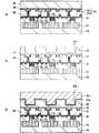
図3は上述した本実施形態の半導体装置の製造に用いる第1基板2の作製手順を示す断面工程図(その1)であり、図4はこの図3に続く断面工程図(その2)である。以下、これらの図に基づいて本実施形態に用いる第1基板2(センサ基板)の作製手順を説明する。≪3. Manufacturing Procedure of First Substrate (Sensor Substrate) in Manufacturing Semiconductor Device of this Embodiment >>
FIG. 3 is a cross-sectional process diagram (part 1) showing a manufacturing procedure of the
図3Aに示すように、例えば単結晶シリコンからなる半導体基板20を用意する。この半導体基板20の所定深さにn型不純物層からなる光電変換部21を形成し、さらに光電変換部21の表面層に、n+型不純物層からなる電荷転送部やp+型不純物層からなる正孔用の電荷蓄積部を形成する。また半導体基板20の表面層に、n+型不純物層からなるフローティングディフュージョンFD、およびソース/ドレイン23、さらにはここでの図示を省略した他の不純物層を形成する。As shown in FIG. 3A, a
次に、半導体基板20上に、ゲート絶縁膜25を成膜し、さらにこの上部に転送ゲートTGおよびゲート電極27を形成する。ここで、転送ゲートTGはフローティングディフュージョンFDと光電変換部21との間に形成され、ゲート電極27は、ソース/ドレイン23間に形成される。またこれと同一工程により、ここでの図示を省略した他の電極を形成する。
なお、ここまでの工程は、通常の作製手順を適宜選択して行なってもよい。Next, a
Note that the steps up to here may be performed by appropriately selecting a normal manufacturing procedure.
その後、ゲート絶縁膜25上に、転送ゲートTGおよびゲート電極27を覆う状態で、例えば酸化シリコンからなる層間絶縁膜29を成膜する。さらに層間絶縁膜29に溝パターンを形成し、この溝パターン内にバリアメタル層31aを介して配線層31bを埋め込んでなる埋込配線31を形成する。この埋込配線31は、必要箇所で転送ゲートTGに接続して形成される。またここでの図示は省略したが、一部の埋込配線31は、必要箇所でソース/ドレイン23に接続して形成される。以上により、埋込配線31を備えた配線層2bを得る。なお、この埋込配線31の形成には、図3B以下を用いて説明する埋込配線技術を適用する。 Thereafter, an
続いて、配線層2b上に、拡散防止絶縁膜32を成膜し、さらにこの上に第1絶縁膜35を成膜する。例えばTEOSガスを用いたCVD法により、TEOS膜からなる第1絶縁膜35を成膜する。その後、この第1絶縁膜35に、以下に説明する埋込配線技術を適用して、第1電極33を形成する。 Subsequently, a diffusion preventing insulating
図3Bに示すように、第1絶縁膜35に溝パターン35aを形成する。ここでの図示は省略したが、溝パターン35aは、必要な箇所では埋込配線31に達する形状で形成される。 As shown in FIG. 3B, a
図3Cに示すように、溝パターン35aの内壁を覆う状態でバリアメタル層33aを成膜し、この上部に溝パターン35aを埋め込む状態で第1電極膜33bを成膜する。バリアメタル層33aは、第1電極膜33bが第1絶縁膜35に拡散することを防ぐようなバリア性のある材料で構成され、一方、第1電極膜33bは銅(Cu)からなるが、これに限らず、導電性のある材料により構成される。 As shown in FIG. 3C, a
図4Dに示すように、CMP法により、バリアメタル層33aが露出するまで第1電極膜33bを平坦化除去し、さらに、第1絶縁膜35が露出するまでバリアメタル層33aを平坦化除去する。これにより、溝パターン35a内にバリアメタル層33aを介して第1電極膜33bを埋め込んでなる第1電極33を形成する。以上により、第1電極33を備えた電極層2cを得る。 As shown in FIG. 4D, the
以上の工程により、第1電極33と第1絶縁膜35とが露出された平坦な貼合せ面41を有する第1基板2が、センサ基板として作製される。なお、必要に応じて、貼合せ面41に対して、ウェット処理またはプラズマ処理による前処理を施しておく。
ここまでの工程は、一般的な半導体装置の製造工程手順で行えばよく、また特に工程手順が限定されることはなく、適宜の手順で行うことができる。ただし、貼り合わせ面となる第1電極33の形成において、銅(Cu)の成膜温度は例えば100℃程度に低くし、貼り合わせ後の熱処理温度(例えば400℃)との温度差を可能な限り大きくする。本開示では、次の絶縁性薄膜の成膜が特徴的な工程となる。Through the above steps, the
The steps so far may be performed according to a general semiconductor device manufacturing process procedure, and the process procedure is not particularly limited, and can be performed according to an appropriate procedure. However, in the formation of the
[絶縁性薄膜の成膜手順]
図4Eに示すように、第1基板2における貼合せ面41の全面を覆う状態で、原子層堆積法(Atomic Layer Deposition:以下ALD法)によって絶縁性薄膜12aを成膜する。[Insulating thin film deposition procedure]
As shown in FIG. 4E, the insulating
ALD法の手順について、概略を説明する。
まず、成膜される薄膜の構成元素を含有する第1反応物と第2反応物とを準備する。成膜工程として、基板上に、第1反応物を含むガスを供給して吸着反応させる第1工程と、第2反応物を含むガス供給して吸着反応させる第2工程とがあり、この工程の間には不活性ガスを流して、未吸着の反応物をパージする。この成膜工程を1サイクル行なうことで原子層1層を堆積させ、繰り返すことにより所望膜厚の成膜をする。なお、第1工程と第2工程は、どちらを先に行なってもよい。
以上のような成膜方法がALD法であり、次のような特徴がある。An outline of the procedure of the ALD method will be described.
First, a first reactant and a second reactant containing constituent elements of a thin film to be formed are prepared. As the film forming process, there are a first process in which a gas containing a first reactant is supplied and subjected to an adsorption reaction on the substrate, and a second process in which a gas containing a second reactant is supplied and subjected to an adsorption reaction. In the meantime, an inert gas is allowed to flow to purge unadsorbed reactants. By performing this film forming process for one cycle, one atomic layer is deposited and repeated to form a film with a desired film thickness. Note that either the first step or the second step may be performed first.
The film formation method as described above is the ALD method and has the following characteristics.
ALD法は、上述のように、成膜工程のサイクルを繰り返して成膜する方法であり、このサイクル数の調整によって、成膜する膜厚を原子層単位で高精度に制御した成膜が可能である。このようなALD法を絶縁性薄膜12aの成膜に適用すると、極めて薄い絶縁性薄膜12aであっても膜厚制御性よく成膜できる。 As described above, the ALD method is a method of forming a film by repeating the cycle of the film forming process. By adjusting the number of cycles, the film thickness can be controlled with high accuracy in units of atomic layers. It is. When such an ALD method is applied to the formation of the insulating
ALD法は、さらに約500℃以下の低温プロセスでの成膜が可能な方法である。さらにSiO2などでは室温での成膜も可能となっている。絶縁性薄膜12aの成膜時には、すでに電極層2cが形成されているため、電極層2cを構成する金属への耐熱性を考慮する必要があり、絶縁性薄膜12aの成膜には低温プロセスが要求される。そこで、このようなALD法を絶縁性薄膜12aの成膜に適用すると、低温プロセスにより電極層2cを劣化させることなく絶縁性薄膜12aを成膜できる。The ALD method is a method capable of forming a film at a low temperature process of about 500 ° C. or lower. Furthermore, film formation at room temperature is possible with SiO2 or the like. Since the
ALD法は、上述のように、原子層を1層ずつ堆積させて成膜する方法である。このようなALD法を絶縁性薄膜12aの成膜に適用すると、CMPにより超平坦化された基板表面の凹凸を悪化させることなく、平坦かつ均一な絶縁性薄膜12で貼合せ面41の全面を覆うことができる。 As described above, the ALD method is a method of forming a film by depositing atomic layers one by one. When such an ALD method is applied to the formation of the insulating
以下に、一例として、酸化膜または窒化膜からなる絶縁性薄膜12aのALD法による成膜条件について、具体的に説明する。 Hereinafter, as an example, film formation conditions by the ALD method of the insulating
絶縁性薄膜12aが酸化膜(SiO2、HfO2等)からなる場合、上述のALD法において、第1反応物をSi含有反応物またはHf含有反応物とし、第2反応物をO含有反応物とする。これらの反応物を供給して吸着反応させる工程を交互に繰り返すことによって、酸化膜(SiO2またはHfO2)からなる絶縁性薄膜12aを貼合せ面41上に成膜する。ここで、Si含有反応物は、例えば、シラン(SiH4)、ジクロロシラン(H2SiCl2)等のガス状で供給可能な物質を用いる。Hf含有反応物は、テトラキスジメチルアミノハフニウム(Hf[N(CH3)2]4等を用いる。O含有反応物は、水蒸気ガス、オゾンガス等を用いる。When the insulating
一方、絶縁性薄膜12aが窒化膜(SiN等)からなる場合、上述のALD法において、第1反応物をSi含有反応物とし、第2反応物をN含有反応物とする。これらの反応物を供給して吸着反応させる工程を交互に繰り返すことによって、窒化膜(SiN)からなる絶縁性薄膜12aを貼合せ面41上に成膜する。ここで、N含有反応物は、例えば、窒素ガスやアンモニアガス等を用いる。O含有反応物は、水蒸気ガス、オゾンガス等を用いる。 On the other hand, when the insulating
以上により、第1基板2上に、貼合せ面41の全面を覆う状態で、極めて薄い均一な絶縁性薄膜12aを成膜する。 As described above, the extremely thin uniform insulating
≪4.本実施形態の半導体装置の製造における第2基板(回路基板)の作製手順≫
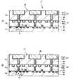
図5は、上述した本実施形態の半導体装置の製造に用いる第2基板7の作製手順を説明するための断面工程図である。以下、この図に基づいて本実施形態に用いる第2基板7(回路基板)の作製手順を説明する。<< 4. Manufacturing Procedure of Second Substrate (Circuit Substrate) in Manufacturing Semiconductor Device of this Embodiment >>
FIG. 5 is a cross-sectional process diagram for explaining a procedure for manufacturing the
図5Aに示すように、例えば単結晶シリコンからなる半導体基板50を用意する。この半導体基板50の表面層に、各導電型のソース/ドレイン51、およびここでの図示を省略した他の不純物層を形成する。これにより、半導体層7aを得る。 As shown in FIG. 5A, a
次に、半導体層7aの上に、ゲート絶縁膜53を成膜し、さらにこの上部にゲート電極55を形成する。ゲート電極55は、ソース/ドレイン51間に形成される。また、これと同一工程で、ここでの図示を省略した他の電極を形成する。 Next, a
続いて、ゲート絶縁膜53の上に、ゲート電極55を覆う状態で、例えば酸化シリコンからなる層間絶縁膜57を成膜する。この層間絶縁膜57の溝パターン内にバリアメタル層59aを介して配線層59bを埋め込んでなる埋込配線59を形成し、埋込配線59を備えた配線層7bを得る。ここでの埋込配線59の形成は、上述した第1電極33の形成と同様に、埋込配線技術を適用して行なう。 Subsequently, an
その後、配線層7b上に拡散防止絶縁膜61を介して、例えばTEOS膜からなる第2絶縁膜69を積層させて成膜する。これにより、第2絶縁膜69の溝パターン内にバリアメタル層67aを介して第2電極膜67bを埋め込んでなる第2電極67を形成し、第2電極67を備えた電極層7cを得る。ここでの第2電極67の形成は、上述した第1電極33の形成と同様にして行なう。 Thereafter, a second insulating
以上の工程により、第2電極67と第2絶縁膜69とが露出された平坦な貼合せ面71を有する第2基板7が、回路基板として作製される。
ここまでの工程は、通常の工程手順で行えばよく、また特に工程手順が限定されることはなく、適宜の手順で行うことができる。ただし、貼り合わせ面となる第2電極67の形成において、銅(Cu)の成膜温度は例えば100℃程度に低くし、貼り合わせ後の熱処理温度(例えば400℃)との温度差を可能な限り大きくする。本開示では、次の絶縁性薄膜の成膜、および基板の貼り合わせが特徴的な工程となる。Through the above steps, the
The steps up to here may be performed according to a normal process procedure, and the process procedure is not particularly limited, and can be performed according to an appropriate procedure. However, in forming the
図5Bに示すように、第1基板2側の絶縁性薄膜12aと同様にして、貼合せ面71の上に、ALD法により絶縁性薄膜12bを成膜する。
これにより、第2基板7上に、貼合せ面71の全面を覆う状態で、極めて薄い均一な絶縁性薄膜12bを成膜する。なお、絶縁性薄膜12bは、第1基板2側の絶縁性薄膜12aと異なる膜でもよいが、同じ膜でもよい。As shown in FIG. 5B, the insulating
Thus, an extremely thin uniform insulating
≪5.本実施形態の半導体装置の製造における基板の貼り合わせ手順≫
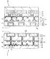
図6および図7を用いて、貼合せ面41上に絶縁性薄膜12aを成膜した第1基板2と、貼合せ面71上に絶縁性薄膜12bを成膜した第2基板7との貼り合わせ手順を説明する。≪5. Procedure for bonding substrates in manufacturing the semiconductor device of this embodiment >>
6 and 7, the
図6に示すように、絶縁性薄膜を介した状態で第1基板2の貼合せ面41と第2基板7の貼合せ面71とを対向配置させ、さらに、第1基板2の第1電極33と、第2基板7の第2電極67とが対応するように位置合わせする。図示した例では、第1電極33と第2電極67とが1:1で対応している状態を示したが、対応状態はこれに限定されることはない。 As shown in FIG. 6, the
図7に示すように、第1基板2上の絶縁性薄膜12aと、第2基板7上の絶縁性薄膜12bとを対向させた状態で熱処理を行うことにより、絶縁性薄膜12aと絶縁性薄膜12bとの間の接合をする。このような熱処理は、第1基板2および第2基板7に形成された素子や配線に影響のない範囲で、絶縁性薄膜12同士が十分に接合する温度および時間で行われる。さらにこのとき、銅(Cu)の結晶粒成長が発生し、第1電極33と第2電極67の間の絶縁性薄膜12を両側から破壊する。これにより、電極の銅(Cu)同士が直接接触する。 As shown in FIG. 7, the insulating
例えば、第1電極33および第2電極67が、銅(Cu)を主とする材料で構成される場合、200℃〜600℃で15分〜5時間程度の熱処理が行われる。このような熱処理は、加圧雰囲気下で行ってもよく、または、第1基板2と第2基板7とを両面側から押圧した状態で行ってもよい。一例として、400℃で4時間の熱処理を行うことで、絶縁性薄膜12を介した第1電極33と第2電極67との間の接続を行なう。これにより、絶縁性薄膜12aと絶縁性薄膜12bとの間が接合され、第1基板2と第2基板7とが貼り合わせられる。ここで、銅(Cu)の成膜時の温度と熱処理の温度差が大きいほど、銅(Cu)の結晶粒成長を促進できるため、絶縁性薄膜12の破壊が容易になる。 For example, when the
ここで、上述のように第1基板2および第2基板7の両方の貼合せ面41,71上に絶縁性薄膜12a,12bが成膜される場合は、その絶縁性薄膜12a,12bが同じ材料であっても、異なる材料であってもよい。 Here, when the insulating
なお、本実施形態の半導体装置の製造方法では、第1基板2および第2基板7のうちどちらか一方の基板の貼合せ面のみに絶縁性薄膜を成膜してもよい。例えば、第1基板2の貼合せ面41上のみに絶縁性薄膜12aを成膜して、第1基板2側の絶縁性薄膜12aと第2基板7側の貼合せ面71との間の接合により、第1基板2と第2基板7を貼り合わせてもよい。 In the semiconductor device manufacturing method of the present embodiment, an insulating thin film may be formed only on the bonding surface of one of the
以上のように、第1基板2と第2基板7とを貼り合わせた後、第1基板2側の半導体基板20を薄膜化して半導体層2aとし、光電変換部21を露出させる。また必要に応じて、第2基板7側の半導体層7aにおいて、半導体基板50を薄膜化してもよい。 As described above, after bonding the
その後は図2に示すように、第1基板2における光電変換部21の露出面上に保護膜15を成膜し、さらに保護膜15上にカラーフィルタ層17およびオンチップレンズ19を形成し、半導体装置(固体撮像装置)1を完成させる。 Thereafter, as shown in FIG. 2, a
[本実施形態の半導体装置の製造方法による効果]
上述のような本実施形態の半導体装置の製造方法では、第1基板2および第2基板7の上にそれぞれ絶縁性薄膜12a,12bを成膜し、この絶縁性薄膜12a,12bが成膜された面同士を接合することにより、第1基板2と第2基板7を貼り合わせている。このため、CMPにより平坦化処理された貼合せ面41,71同士を直接接合する場合と比較して、絶縁性薄膜12a,12bが成膜された面同士の接合によって、第1基板2と第2基板7を貼り合わせる本実施形態の半導体装置1は接合性がよい。なお、第1基板2の貼合せ面41上にのみ絶縁性薄膜12aを成膜した場合であっても、第1基板2側の絶縁性薄膜12aと第2基板7側の貼合せ面71との間の接合になり、貼合せ面41,71同士を直接接合する場合よりも基板の接合性がよい。[Effects of Semiconductor Device Manufacturing Method of Present Embodiment]
In the manufacturing method of the semiconductor device according to the present embodiment as described above, the insulating
例えば、CMPにより平坦化処理された貼合せ面41,71は、CMPの工程において貼合せ面41,71を構成する第1絶縁膜35および第2絶縁膜69が含水する可能性がある。また、この貼合せ面41,71を構成する第1絶縁膜35および第2絶縁膜69がTEOS膜からなる場合であれば、そのTEOS膜の成膜条件ゆえに、もともと含水率の高い膜として第1絶縁膜35および第2絶縁膜69が形成される。したがって、このような含水している貼合せ面41,71同士を直接接合する場合、貼合せ後の熱処理において、脱ガスが接合界面に集中しボイドを形成する。しかしながら、本実施形態では、貼合せ面41,71の全面を絶縁性薄膜12a,12bで覆うことにより、脱ガスが接合界面に集中することを防止しボイドの発生を抑えることが可能である。 For example, the bonding surfaces 41 and 71 that have been planarized by CMP may contain water in the first insulating
特に、第1基板2の貼合せ面41上の絶縁性薄膜12aと第2基板7の貼合せ面71上の絶縁性薄膜12bが、同一材料膜で構成されている場合は、同一材料膜同士の接合となるので、より強固な接合が可能になる。これにより、基板の接合強度が増して信頼性の向上が図られた半導体装置を得ることができる。 In particular, when the insulating
さらには、絶縁性薄膜12a,12bの成膜をALD法により行なったことにより、次のような効果もある。 Furthermore, since the insulating
まず、ALD法は原子層単位の成膜により膜厚制御性のよい方法なので、極めて薄い絶縁性薄膜を成膜できる。これにより、第1基板2側の第1電極33と第2基板7側の第2電極67とが絶縁性薄膜12を介して対向配置された構造であっても、この絶縁性薄膜12が極めて薄い膜厚であるので、第1電極33と第2電極67との間の電気的な接続が可能となる。 First, since the ALD method is a method with good film thickness controllability by film formation in units of atomic layers, an extremely thin insulating thin film can be formed. Thus, even if the
次に、ALD法は原子層単位の成膜により膜厚均一性のよい方法なので、CMPにより平坦化された貼合せ面41,71の平坦性を維持して、均一な絶縁性薄膜12a,12bを第1基板2および第2基板7の上に成膜する。このような絶縁性薄膜12a,12bの成膜された平坦な接合面同士によって接合が図られるので、密着性に優れた接合が行なわれ、接合強度の向上した基板の接合が可能となる。 Next, since the ALD method is a method with good film thickness uniformity by film formation in units of atomic layers, the flatness of the bonding surfaces 41 and 71 flattened by CMP is maintained, and the uniform insulating
続いて、ALD法は低温プロセスでの成膜をする方法なので、第1基板2側の電極層2cおよび第2基板7側の電極層7cを構成する金属が高熱により劣化することなく、第1基板2および第2基板7の上に絶縁性薄膜12a,12bを成膜できる。従って、本開示の要点である、銅(Cu)の結晶粒成長を貼り合わせ後の熱処理で促進する目的に適している。ここまでALD法による利点を記述したが、CVD法による方法であっても、上述した利点を実現できるのであればALD法による成膜にはこだわらない。さらに、ガスを用いた気相成長による成膜以外でも、例えば塗布方法などによる成膜であっても、本開示の原理を実現できる薄膜が形成出来れば良い。 Subsequently, since the ALD method is a method of forming a film by a low temperature process, the metal constituting the
最後に、ALD法は原子層単位の成膜方法なので、成膜された絶縁性薄膜12a,12bは緻密な膜であって含水率が極めて低い。含水率の低い絶縁性薄膜12a,12bの成膜された接合面同士による接合となるので、接合面にボイドの発生する虞は全くない。
以上により、基板の接合強度が増して信頼性の向上が図られた半導体装置が得られる。Finally, since the ALD method is a film formation method in units of atomic layers, the formed insulating
Thus, a semiconductor device in which the bonding strength of the substrate is increased and the reliability is improved can be obtained.
≪6.本実施形態の半導体装置を用いた電子機器の一例≫
上述の本実施形態で説明した本開示に係る半導体装置(固体撮像装置)は、例えばデジタルカメラやビデオカメラ等のカメラシステム、さらには撮像機能を有する携帯電話、あるいは撮像機能を備えた他の機器などの電子機器に適用することができる。≪6. Example of Electronic Device Using Semiconductor Device of this Embodiment >>
The semiconductor device (solid-state imaging device) according to the present disclosure described in the above-described embodiment includes, for example, a camera system such as a digital camera or a video camera, a mobile phone having an imaging function, or another device having an imaging function. It can be applied to such electronic devices.
図8は、本開示に係る電子機器の一例として、固体撮像装置を用いたカメラの構成図を示す。本実施形態に係るカメラ91は、静止画像又は動画撮影可能なビデオカメラを例としたものである。このカメラ91は、固体撮像装置92と、固体撮像装置92の光電変換部に入射光を導く光学系93と、シャッタ装置94と、固体撮像装置92を駆動する駆動回路95と、固体撮像装置92の出力信号を処理する信号処理回路96とを有する。 FIG. 8 is a configuration diagram of a camera using a solid-state imaging device as an example of the electronic apparatus according to the present disclosure. The
固体撮像装置92は、上述した本実施形態で説明した構成の半導体装置(1)が適用される。光学系(光学レンズ)93は、被写体からの像光(入射光)を固体撮像装置92の撮像面上に結像させる。これにより、固体撮像装置92内に、一定期間信号電荷が蓄積される。このような光学系93は、複数の光学レンズから構成された光学レンズ系としてもよい。シャッタ装置94は、固体撮像装置92への光照射期間および遮光期間を制御する。駆動回路95は、固体撮像装置92およびシャッタ装置94に駆動信号を供給し、供給した駆動信号(タイミング信号)により、固体撮像装置92の信号処理回路96への信号出力動作の制御、およびシャッタ装置94のシャッタ動作を制御する。すなわち、駆動回路95は、駆動信号(タイミング信号)の供給により、固体撮像装置92から信号処理回路96への信号転送動作を行う。信号処理回路96は、固体撮像装置92から転送された信号に対して、各種の信号処理を行う。信号処理が行われた映像信号は、メモリなどの記憶媒体に記憶され、或いは、モニタに出力される。 As the solid-
以上説明した本実施形態に係る電子機器によれば、センサ基板と回路基板とを積層させた信頼性の高い3次元構造の半導体装置1を固体撮像装置として用いたことにより、撮像機能を有する電子機器の小型化および信頼性の向上を図ることが可能になる。 According to the electronic device according to the present embodiment described above, an electronic device having an imaging function is obtained by using the highly reliable three-
1 半導体装置, 2 第1基板(センサ基板), 7 第2基板(回路基板), 12 絶縁性薄膜, 33 第1電極, 35 第1絶縁膜, 41,71 貼合せ面, 67 第2電極, 69 第2絶縁膜 DESCRIPTION OF
Claims (5)
Translated fromJapanese電極および絶縁膜が露出された貼合せ面を有する2枚の基板のうち少なくとも一方の貼合せ面を覆う状態で、絶縁性薄膜を成膜し、
前記絶縁性薄膜を介して前記2枚の基板の貼合せ面同士を対向配置し、
前記2枚の基板の電極同士が前記絶縁性薄膜を介して電気的に接続される状態に位置合わせをして、前記2枚の基板を貼り合わせ、
貼り合わされた前記2枚の基板を、前記電極の成膜温度よりも高温で熱処理して、前記電極同士で狭持された絶縁性薄膜を、対応する電極それぞれを構成する金属の結晶粒成長による変形・移動によって破壊し、前記電極同士を直接接触させる
製造方法。In a method for manufacturing a semiconductor device,
An insulating thin film is formed in a state where at least one of the two substrates having the bonding surface from which the electrode and the insulating film are exposed is covered,
Place the bonding surfaces of the two substrates opposite to each other through the insulating thin film,
Position the electrodes of the two substrates to be in an electrically connected state via the insulating thin film, and bond the two substrates together.
The bonded two substrates are heat-treated at a temperature higher than the film forming temperature of the electrodes, and the insulating thin film held between the electrodes is grown by crystal grain growth of the metal constituting each of the corresponding electrodes. A manufacturing method in which the electrodes are directly brought into contact with each other by being broken by deformation or movement.
請求項1に記載の製造方法。Wherein both the two substrates, the manufacturing method according to claim1 of forming the insulating thin film.
請求項1または2に記載の製造方法。Wherein both the two substrates, the manufacturing method according to claim1 or2 for forming the insulating thin film made of the same material.
請求項1から3のいずれかに記載の製造方法。The process according to any one of claims1 to3, depositing said insulating thin film by atomic layer deposition.
請求項1から4のいずれかに記載の製造方法。The cemented surface of the two substrates, the manufacturing method according to claim1 formed4 of the planarization process.
Priority Applications (13)
| Application Number | Priority Date | Filing Date | Title |
|---|---|---|---|
| JP2013060691AJP5939184B2 (en) | 2013-03-22 | 2013-03-22 | Manufacturing method of semiconductor device |
| TW103104291ATWI614880B (en) | 2013-03-22 | 2014-02-10 | Semiconductor device and manufacturing method |
| KR1020140020012AKR102158394B1 (en) | 2013-03-22 | 2014-02-21 | Semiconductor device and manufacturing method |
| US14/206,489US9190275B2 (en) | 2013-03-22 | 2014-03-12 | Bonding substrates with electrical connection through insulating film |
| CN201910445485.8ACN110190076B (en) | 2013-03-22 | 2014-03-14 | Semiconductor device and method of manufacture |
| CN201410095150.5ACN104064574B (en) | 2013-03-22 | 2014-03-14 | Semiconductor device and manufacturing method |
| CN201910468930.2ACN110211979B (en) | 2013-03-22 | 2014-03-14 | Photodetector and method for manufacturing the same |
| CN201810156644.8ACN108198834A (en) | 2013-03-22 | 2014-03-14 | Semiconductor device and manufacturing method |
| US14/880,957US9666627B2 (en) | 2013-03-22 | 2015-10-12 | Electronic apparatus and manufacturing method for an electronic apparatus having multiple substrates directly electrically connected through an insulating film |
| US15/607,845US10134795B2 (en) | 2013-03-22 | 2017-05-30 | Semiconductor device with multiple substrates electrically connected through an insulating film and manufacturing method |
| US15/987,278US10707258B2 (en) | 2013-03-22 | 2018-05-23 | Semiconductor device with multiple substrates electrically connected through an insulating film |
| US16/554,347US11107855B2 (en) | 2013-03-22 | 2019-08-28 | Method for bonding and connecting substrates |
| US17/392,733US20210366958A1 (en) | 2013-03-22 | 2021-08-03 | Semiconductor device and manufacturing method |
Applications Claiming Priority (1)
| Application Number | Priority Date | Filing Date | Title |
|---|---|---|---|
| JP2013060691AJP5939184B2 (en) | 2013-03-22 | 2013-03-22 | Manufacturing method of semiconductor device |
Publications (3)
| Publication Number | Publication Date |
|---|---|
| JP2014187166A JP2014187166A (en) | 2014-10-02 |
| JP2014187166A5 JP2014187166A5 (en) | 2015-03-19 |
| JP5939184B2true JP5939184B2 (en) | 2016-06-22 |
Family
ID=51552209
Family Applications (1)
| Application Number | Title | Priority Date | Filing Date |
|---|---|---|---|
| JP2013060691AActiveJP5939184B2 (en) | 2013-03-22 | 2013-03-22 | Manufacturing method of semiconductor device |
Country Status (5)
| Country | Link |
|---|---|
| US (6) | US9190275B2 (en) |
| JP (1) | JP5939184B2 (en) |
| KR (1) | KR102158394B1 (en) |
| CN (4) | CN110190076B (en) |
| TW (1) | TWI614880B (en) |
Families Citing this family (27)
| Publication number | Priority date | Publication date | Assignee | Title |
|---|---|---|---|---|
| JP5517800B2 (en)* | 2010-07-09 | 2014-06-11 | キヤノン株式会社 | Member for solid-state imaging device and method for manufacturing solid-state imaging device |
| JP5682327B2 (en) | 2011-01-25 | 2015-03-11 | ソニー株式会社 | Solid-state imaging device, manufacturing method of solid-state imaging device, and electronic apparatus |
| JP5939184B2 (en)* | 2013-03-22 | 2016-06-22 | ソニー株式会社 | Manufacturing method of semiconductor device |
| TWI648986B (en)* | 2014-04-15 | 2019-01-21 | 日商新力股份有限公司 | Image element, electronic equipment |
| TWI676280B (en)* | 2014-04-18 | 2019-11-01 | 日商新力股份有限公司 | Solid-state imaging device and electronic device therewith |
| JP6570417B2 (en)* | 2014-10-24 | 2019-09-04 | 株式会社半導体エネルギー研究所 | Imaging apparatus and electronic apparatus |
| US9761730B2 (en)* | 2014-10-29 | 2017-09-12 | Semiconductor Energy Laboratory Co., Ltd. | Imaging device and electronic device |
| JP6335099B2 (en) | 2014-11-04 | 2018-05-30 | 東芝メモリ株式会社 | Semiconductor device and manufacturing method of semiconductor device |
| JP2016174016A (en)* | 2015-03-16 | 2016-09-29 | 株式会社東芝 | Semiconductor device and manufacturing method of semiconductor device |
| JP2016181531A (en)* | 2015-03-23 | 2016-10-13 | ソニー株式会社 | Semiconductor device, semiconductor device manufacturing method, solid state image pickup element, image pickup device and electronic apparatus |
| JP2017117828A (en)* | 2015-12-21 | 2017-06-29 | ソニー株式会社 | Solid-state imaging device and electronic device |
| US11405569B2 (en)* | 2017-07-25 | 2022-08-02 | Sony Semiconductor Solutions Corporation | Solid-state imaging device |
| TW202315106A (en)* | 2017-10-30 | 2023-04-01 | 日商索尼半導體解決方案公司 | Solid-state imaging device, and electronic apparatus |
| CN112640112B (en)* | 2018-10-15 | 2025-02-25 | 索尼半导体解决方案公司 | Solid-state imaging device and electronic equipment |
| CN110233980B (en)* | 2019-06-27 | 2021-11-02 | Oppo广东移动通信有限公司 | Active pixel image sensor, image processing method, and storage medium |
| KR102780353B1 (en)* | 2019-08-26 | 2025-03-12 | 삼성전자주식회사 | Semiconductor device and method of manufacturing the same |
| US11094653B2 (en)* | 2019-11-13 | 2021-08-17 | Sandisk Technologies Llc | Bonded assembly containing a dielectric bonding pattern definition layer and methods of forming the same |
| CN112885777B (en) | 2020-01-07 | 2022-12-09 | 长江存储科技有限责任公司 | Metal-dielectric bonding method and structure |
| US20230139201A1 (en)* | 2020-03-31 | 2023-05-04 | Sony Semiconductor Solutions Corporation | Imaging element and method for manufacturing imaging element |
| US12199018B2 (en)* | 2020-09-18 | 2025-01-14 | Intel Corporation | Direct bonding in microelectronic assemblies |
| US11990448B2 (en) | 2020-09-18 | 2024-05-21 | Intel Corporation | Direct bonding in microelectronic assemblies |
| WO2022176687A1 (en)* | 2021-02-22 | 2022-08-25 | 東京エレクトロン株式会社 | Semiconductor device, joining method, and joining system |
| US12094849B2 (en)* | 2021-07-22 | 2024-09-17 | Taiwan Semiconductor Manufacturing Company, Ltd. | Atomic layer deposition bonding layer for joining two semiconductor devices |
| KR20230052360A (en)* | 2021-10-12 | 2023-04-20 | 삼성전자주식회사 | Semiconductor package and method of manufacturing the same |
| JP2023137581A (en)* | 2022-03-18 | 2023-09-29 | キオクシア株式会社 | Semiconductor device and manufacturing method thereof |
| US20230411325A1 (en)* | 2022-06-15 | 2023-12-21 | Xilinx, Inc. | Chip package integration with hybrid bonding |
| WO2024024450A1 (en)* | 2022-07-26 | 2024-02-01 | ソニーセミコンダクタソリューションズ株式会社 | Semiconductor device and manufacturing method for same |
Family Cites Families (22)
| Publication number | Priority date | Publication date | Assignee | Title |
|---|---|---|---|---|
| JP3663786B2 (en)* | 1996-10-14 | 2005-06-22 | ヤマハ株式会社 | Semiconductor chip mounting method and structure |
| JP3532788B2 (en) | 1999-04-13 | 2004-05-31 | 唯知 須賀 | Semiconductor device and manufacturing method thereof |
| WO2004059720A1 (en) | 2002-12-20 | 2004-07-15 | International Business Machines Corporation | Three-dimensional device fabrication method |
| KR100610481B1 (en) | 2004-12-30 | 2006-08-08 | 매그나칩 반도체 유한회사 | Image sensor with wider light receiving area and manufacturing method |
| GB2430172B (en)* | 2005-08-01 | 2009-04-15 | Honda Motor Co Ltd | Method of and apparatus for manufacturing joined body |
| JP2007049040A (en)* | 2005-08-11 | 2007-02-22 | Omron Corp | Joining method |
| US8288184B2 (en)* | 2007-12-18 | 2012-10-16 | Sharp Kabushiki Kaisha | Production method of semiconductor device and semiconductor device |
| JP2010066723A (en)* | 2008-09-12 | 2010-03-25 | Kobe Steel Ltd | Method for manufacturing display device |
| JP2010129576A (en) | 2008-11-25 | 2010-06-10 | Nikon Corp | Lamination semiconductor substrate, and method of manufacturing lamination semiconductor substrate |
| KR20100129576A (en) | 2009-06-01 | 2010-12-09 | 주식회사 유니온 메디칼 | Stamp with Micro Needle |
| EP2518768B1 (en)* | 2009-12-26 | 2019-03-20 | Canon Kabushiki Kaisha | Solid-state imaging device and imaging system |
| JP5843475B2 (en)* | 2010-06-30 | 2016-01-13 | キヤノン株式会社 | Solid-state imaging device and method for manufacturing solid-state imaging device |
| US8377798B2 (en)* | 2010-11-10 | 2013-02-19 | Taiwan Semiconductor Manufacturing Co., Ltd | Method and structure for wafer to wafer bonding in semiconductor packaging |
| US8778773B2 (en)* | 2010-12-16 | 2014-07-15 | Soitec | Methods for directly bonding together semiconductor structures, and bonded semiconductor structures formed using such methods |
| TWI458072B (en)* | 2010-12-16 | 2014-10-21 | Soitec Silicon On Insulator | Methods for directly bonding together semiconductor structures, and bonded semiconductor structures formed using such methods |
| US8716105B2 (en)* | 2011-03-31 | 2014-05-06 | Soitec | Methods for bonding semiconductor structures involving annealing processes, and bonded semiconductor structures and intermediate structures formed using such methods |
| CN102751266B (en)* | 2011-04-21 | 2016-02-03 | 精材科技股份有限公司 | Chip package and method for forming the same |
| JP5919653B2 (en) | 2011-06-09 | 2016-05-18 | ソニー株式会社 | Semiconductor device |
| US8896125B2 (en)* | 2011-07-05 | 2014-11-25 | Sony Corporation | Semiconductor device, fabrication method for a semiconductor device and electronic apparatus |
| US8697493B2 (en)* | 2011-07-18 | 2014-04-15 | Soitec | Bonding surfaces for direct bonding of semiconductor structures |
| US8916448B2 (en)* | 2013-01-09 | 2014-12-23 | International Business Machines Corporation | Metal to metal bonding for stacked (3D) integrated circuits |
| JP5939184B2 (en)* | 2013-03-22 | 2016-06-22 | ソニー株式会社 | Manufacturing method of semiconductor device |
- 2013
- 2013-03-22JPJP2013060691Apatent/JP5939184B2/enactiveActive
- 2014
- 2014-02-10TWTW103104291Apatent/TWI614880B/enactive
- 2014-02-21KRKR1020140020012Apatent/KR102158394B1/enactiveActive
- 2014-03-12USUS14/206,489patent/US9190275B2/enactiveActive
- 2014-03-14CNCN201910445485.8Apatent/CN110190076B/enactiveActive
- 2014-03-14CNCN201910468930.2Apatent/CN110211979B/enactiveActive
- 2014-03-14CNCN201810156644.8Apatent/CN108198834A/enactivePending
- 2014-03-14CNCN201410095150.5Apatent/CN104064574B/enactiveActive
- 2015
- 2015-10-12USUS14/880,957patent/US9666627B2/enactiveActive
- 2017
- 2017-05-30USUS15/607,845patent/US10134795B2/enactiveActive
- 2018
- 2018-05-23USUS15/987,278patent/US10707258B2/enactiveActive
- 2019
- 2019-08-28USUS16/554,347patent/US11107855B2/enactiveActive
- 2021
- 2021-08-03USUS17/392,733patent/US20210366958A1/ennot_activeAbandoned
Also Published As
| Publication number | Publication date |
|---|---|
| US20190386056A1 (en) | 2019-12-19 |
| US20160035777A1 (en) | 2016-02-04 |
| US11107855B2 (en) | 2021-08-31 |
| CN108198834A (en) | 2018-06-22 |
| US10707258B2 (en) | 2020-07-07 |
| KR20140115948A (en) | 2014-10-01 |
| JP2014187166A (en) | 2014-10-02 |
| US20170263666A1 (en) | 2017-09-14 |
| CN110211979B (en) | 2022-11-18 |
| CN104064574B (en) | 2019-06-07 |
| US20180269248A1 (en) | 2018-09-20 |
| TWI614880B (en) | 2018-02-11 |
| CN110190076A (en) | 2019-08-30 |
| US10134795B2 (en) | 2018-11-20 |
| CN104064574A (en) | 2014-09-24 |
| US9666627B2 (en) | 2017-05-30 |
| TW201438208A (en) | 2014-10-01 |
| US20140284744A1 (en) | 2014-09-25 |
| CN110190076B (en) | 2022-12-16 |
| US9190275B2 (en) | 2015-11-17 |
| CN110211979A (en) | 2019-09-06 |
| US20210366958A1 (en) | 2021-11-25 |
| KR102158394B1 (en) | 2020-09-21 |
Similar Documents
| Publication | Publication Date | Title |
|---|---|---|
| JP5939184B2 (en) | Manufacturing method of semiconductor device | |
| JP6127360B2 (en) | Semiconductor device and manufacturing method of semiconductor device | |
| US11569123B2 (en) | Semiconductor device, fabrication method for a semiconductor device and electronic apparatus | |
| JP5994274B2 (en) | SEMICONDUCTOR DEVICE, SEMICONDUCTOR DEVICE MANUFACTURING METHOD, AND ELECTRONIC DEVICE | |
| KR102673911B1 (en) | Semiconductor device, fabrication method for a semiconductor device and electronic device | |
| JP5982748B2 (en) | SEMICONDUCTOR DEVICE, SEMICONDUCTOR DEVICE MANUFACTURING METHOD, AND ELECTRONIC DEVICE | |
| CN103022062B (en) | Solid-state imaging device, manufacturing method thereof, and electronic device | |
| JP6031765B2 (en) | SEMICONDUCTOR DEVICE, ELECTRONIC DEVICE, AND METHOD FOR MANUFACTURING SEMICONDUCTOR DEVICE | |
| US7393715B2 (en) | Manufacturing method for image pickup apparatus | |
| JP5975617B2 (en) | Solid-state imaging device, manufacturing method thereof, and camera | |
| US10998370B2 (en) | Semiconductor device with insulating layers forming a bonding plane between first and second circuit components, method of manufacturing the same, and electronic device |
Legal Events
| Date | Code | Title | Description |
|---|---|---|---|
| A521 | Request for written amendment filed | Free format text:JAPANESE INTERMEDIATE CODE: A523 Effective date:20150129 | |
| A621 | Written request for application examination | Free format text:JAPANESE INTERMEDIATE CODE: A621 Effective date:20150129 | |
| A977 | Report on retrieval | Free format text:JAPANESE INTERMEDIATE CODE: A971007 Effective date:20150410 | |
| A131 | Notification of reasons for refusal | Free format text:JAPANESE INTERMEDIATE CODE: A131 Effective date:20150507 | |
| A521 | Request for written amendment filed | Free format text:JAPANESE INTERMEDIATE CODE: A523 Effective date:20150623 | |
| A131 | Notification of reasons for refusal | Free format text:JAPANESE INTERMEDIATE CODE: A131 Effective date:20151013 | |
| A521 | Request for written amendment filed | Free format text:JAPANESE INTERMEDIATE CODE: A523 Effective date:20151127 | |
| TRDD | Decision of grant or rejection written | ||
| A01 | Written decision to grant a patent or to grant a registration (utility model) | Free format text:JAPANESE INTERMEDIATE CODE: A01 Effective date:20160419 | |
| A61 | First payment of annual fees (during grant procedure) | Free format text:JAPANESE INTERMEDIATE CODE: A61 Effective date:20160502 | |
| R151 | Written notification of patent or utility model registration | Ref document number:5939184 Country of ref document:JP Free format text:JAPANESE INTERMEDIATE CODE: R151 | |
| R250 | Receipt of annual fees | Free format text:JAPANESE INTERMEDIATE CODE: R250 | |
| R250 | Receipt of annual fees | Free format text:JAPANESE INTERMEDIATE CODE: R250 |