JP5939055B2 - Semiconductor device and manufacturing method of semiconductor device - Google Patents
Semiconductor device and manufacturing method of semiconductor deviceDownload PDFInfo
- Publication number
- JP5939055B2 JP5939055B2JP2012145086AJP2012145086AJP5939055B2JP 5939055 B2JP5939055 B2JP 5939055B2JP 2012145086 AJP2012145086 AJP 2012145086AJP 2012145086 AJP2012145086 AJP 2012145086AJP 5939055 B2JP5939055 B2JP 5939055B2
- Authority
- JP
- Japan
- Prior art keywords
- semiconductor chips
- resistance
- parallel circuit
- semiconductor
- semiconductor device
- Prior art date
- Legal status (The legal status is an assumption and is not a legal conclusion. Google has not performed a legal analysis and makes no representation as to the accuracy of the status listed.)
- Active
Links
Images


Classifications
- H—ELECTRICITY
- H01—ELECTRIC ELEMENTS
- H01L—SEMICONDUCTOR DEVICES NOT COVERED BY CLASS H10
- H01L23/00—Details of semiconductor or other solid state devices
- H01L23/48—Arrangements for conducting electric current to or from the solid state body in operation, e.g. leads, terminal arrangements ; Selection of materials therefor
- H—ELECTRICITY
- H01—ELECTRIC ELEMENTS
- H01L—SEMICONDUCTOR DEVICES NOT COVERED BY CLASS H10
- H01L22/00—Testing or measuring during manufacture or treatment; Reliability measurements, i.e. testing of parts without further processing to modify the parts as such; Structural arrangements therefor
- H01L22/10—Measuring as part of the manufacturing process
- H01L22/14—Measuring as part of the manufacturing process for electrical parameters, e.g. resistance, deep-levels, CV, diffusions by electrical means
- H—ELECTRICITY
- H01—ELECTRIC ELEMENTS
- H01L—SEMICONDUCTOR DEVICES NOT COVERED BY CLASS H10
- H01L22/00—Testing or measuring during manufacture or treatment; Reliability measurements, i.e. testing of parts without further processing to modify the parts as such; Structural arrangements therefor
- H01L22/20—Sequence of activities consisting of a plurality of measurements, corrections, marking or sorting steps
- H—ELECTRICITY
- H01—ELECTRIC ELEMENTS
- H01L—SEMICONDUCTOR DEVICES NOT COVERED BY CLASS H10
- H01L25/00—Assemblies consisting of a plurality of semiconductor or other solid state devices
- H01L25/03—Assemblies consisting of a plurality of semiconductor or other solid state devices all the devices being of a type provided for in a single subclass of subclasses H10B, H10D, H10F, H10H, H10K or H10N, e.g. assemblies of rectifier diodes
- H01L25/04—Assemblies consisting of a plurality of semiconductor or other solid state devices all the devices being of a type provided for in a single subclass of subclasses H10B, H10D, H10F, H10H, H10K or H10N, e.g. assemblies of rectifier diodes the devices not having separate containers
- H01L25/07—Assemblies consisting of a plurality of semiconductor or other solid state devices all the devices being of a type provided for in a single subclass of subclasses H10B, H10D, H10F, H10H, H10K or H10N, e.g. assemblies of rectifier diodes the devices not having separate containers the devices being of a type provided for in group subclass H10D
- H01L25/072—Assemblies consisting of a plurality of semiconductor or other solid state devices all the devices being of a type provided for in a single subclass of subclasses H10B, H10D, H10F, H10H, H10K or H10N, e.g. assemblies of rectifier diodes the devices not having separate containers the devices being of a type provided for in group subclass H10D the devices being arranged next to each other
- H—ELECTRICITY
- H01—ELECTRIC ELEMENTS
- H01L—SEMICONDUCTOR DEVICES NOT COVERED BY CLASS H10
- H01L25/00—Assemblies consisting of a plurality of semiconductor or other solid state devices
- H01L25/18—Assemblies consisting of a plurality of semiconductor or other solid state devices the devices being of the types provided for in two or more different main groups of the same subclass of H10B, H10D, H10F, H10H, H10K or H10N
- H—ELECTRICITY
- H10—SEMICONDUCTOR DEVICES; ELECTRIC SOLID-STATE DEVICES NOT OTHERWISE PROVIDED FOR
- H10D—INORGANIC ELECTRIC SEMICONDUCTOR DEVICES
- H10D89/00—Aspects of integrated devices not covered by groups H10D84/00 - H10D88/00
- H—ELECTRICITY
- H01—ELECTRIC ELEMENTS
- H01L—SEMICONDUCTOR DEVICES NOT COVERED BY CLASS H10
- H01L2224/00—Indexing scheme for arrangements for connecting or disconnecting semiconductor or solid-state bodies and methods related thereto as covered by H01L24/00
- H01L2224/01—Means for bonding being attached to, or being formed on, the surface to be connected, e.g. chip-to-package, die-attach, "first-level" interconnects; Manufacturing methods related thereto
- H01L2224/02—Bonding areas; Manufacturing methods related thereto
- H01L2224/04—Structure, shape, material or disposition of the bonding areas prior to the connecting process
- H01L2224/06—Structure, shape, material or disposition of the bonding areas prior to the connecting process of a plurality of bonding areas
- H01L2224/0601—Structure
- H01L2224/0603—Bonding areas having different sizes, e.g. different heights or widths
- H—ELECTRICITY
- H01—ELECTRIC ELEMENTS
- H01L—SEMICONDUCTOR DEVICES NOT COVERED BY CLASS H10
- H01L2224/00—Indexing scheme for arrangements for connecting or disconnecting semiconductor or solid-state bodies and methods related thereto as covered by H01L24/00
- H01L2224/01—Means for bonding being attached to, or being formed on, the surface to be connected, e.g. chip-to-package, die-attach, "first-level" interconnects; Manufacturing methods related thereto
- H01L2224/42—Wire connectors; Manufacturing methods related thereto
- H01L2224/47—Structure, shape, material or disposition of the wire connectors after the connecting process
- H01L2224/48—Structure, shape, material or disposition of the wire connectors after the connecting process of an individual wire connector
- H01L2224/481—Disposition
- H01L2224/48151—Connecting between a semiconductor or solid-state body and an item not being a semiconductor or solid-state body, e.g. chip-to-substrate, chip-to-passive
- H01L2224/48221—Connecting between a semiconductor or solid-state body and an item not being a semiconductor or solid-state body, e.g. chip-to-substrate, chip-to-passive the body and the item being stacked
- H01L2224/48225—Connecting between a semiconductor or solid-state body and an item not being a semiconductor or solid-state body, e.g. chip-to-substrate, chip-to-passive the body and the item being stacked the item being non-metallic, e.g. insulating substrate with or without metallisation
- H01L2224/48227—Connecting between a semiconductor or solid-state body and an item not being a semiconductor or solid-state body, e.g. chip-to-substrate, chip-to-passive the body and the item being stacked the item being non-metallic, e.g. insulating substrate with or without metallisation connecting the wire to a bond pad of the item
- H—ELECTRICITY
- H01—ELECTRIC ELEMENTS
- H01L—SEMICONDUCTOR DEVICES NOT COVERED BY CLASS H10
- H01L2224/00—Indexing scheme for arrangements for connecting or disconnecting semiconductor or solid-state bodies and methods related thereto as covered by H01L24/00
- H01L2224/01—Means for bonding being attached to, or being formed on, the surface to be connected, e.g. chip-to-package, die-attach, "first-level" interconnects; Manufacturing methods related thereto
- H01L2224/42—Wire connectors; Manufacturing methods related thereto
- H01L2224/47—Structure, shape, material or disposition of the wire connectors after the connecting process
- H01L2224/49—Structure, shape, material or disposition of the wire connectors after the connecting process of a plurality of wire connectors
- H01L2224/491—Disposition
- H01L2224/4911—Disposition the connectors being bonded to at least one common bonding area, e.g. daisy chain
- H01L2224/49111—Disposition the connectors being bonded to at least one common bonding area, e.g. daisy chain the connectors connecting two common bonding areas, e.g. Litz or braid wires
- H—ELECTRICITY
- H01—ELECTRIC ELEMENTS
- H01L—SEMICONDUCTOR DEVICES NOT COVERED BY CLASS H10
- H01L2224/00—Indexing scheme for arrangements for connecting or disconnecting semiconductor or solid-state bodies and methods related thereto as covered by H01L24/00
- H01L2224/01—Means for bonding being attached to, or being formed on, the surface to be connected, e.g. chip-to-package, die-attach, "first-level" interconnects; Manufacturing methods related thereto
- H01L2224/42—Wire connectors; Manufacturing methods related thereto
- H01L2224/47—Structure, shape, material or disposition of the wire connectors after the connecting process
- H01L2224/49—Structure, shape, material or disposition of the wire connectors after the connecting process of a plurality of wire connectors
- H01L2224/491—Disposition
- H01L2224/4912—Layout
- H01L2224/49175—Parallel arrangements
- H—ELECTRICITY
- H01—ELECTRIC ELEMENTS
- H01L—SEMICONDUCTOR DEVICES NOT COVERED BY CLASS H10
- H01L24/00—Arrangements for connecting or disconnecting semiconductor or solid-state bodies; Methods or apparatus related thereto
- H01L24/01—Means for bonding being attached to, or being formed on, the surface to be connected, e.g. chip-to-package, die-attach, "first-level" interconnects; Manufacturing methods related thereto
- H01L24/42—Wire connectors; Manufacturing methods related thereto
- H01L24/47—Structure, shape, material or disposition of the wire connectors after the connecting process
- H01L24/48—Structure, shape, material or disposition of the wire connectors after the connecting process of an individual wire connector
- H—ELECTRICITY
- H01—ELECTRIC ELEMENTS
- H01L—SEMICONDUCTOR DEVICES NOT COVERED BY CLASS H10
- H01L24/00—Arrangements for connecting or disconnecting semiconductor or solid-state bodies; Methods or apparatus related thereto
- H01L24/01—Means for bonding being attached to, or being formed on, the surface to be connected, e.g. chip-to-package, die-attach, "first-level" interconnects; Manufacturing methods related thereto
- H01L24/42—Wire connectors; Manufacturing methods related thereto
- H01L24/47—Structure, shape, material or disposition of the wire connectors after the connecting process
- H01L24/49—Structure, shape, material or disposition of the wire connectors after the connecting process of a plurality of wire connectors
- H—ELECTRICITY
- H01—ELECTRIC ELEMENTS
- H01L—SEMICONDUCTOR DEVICES NOT COVERED BY CLASS H10
- H01L2924/00—Indexing scheme for arrangements or methods for connecting or disconnecting semiconductor or solid-state bodies as covered by H01L24/00
- H01L2924/0001—Technical content checked by a classifier
- H01L2924/00014—Technical content checked by a classifier the subject-matter covered by the group, the symbol of which is combined with the symbol of this group, being disclosed without further technical details
- H—ELECTRICITY
- H01—ELECTRIC ELEMENTS
- H01L—SEMICONDUCTOR DEVICES NOT COVERED BY CLASS H10
- H01L2924/00—Indexing scheme for arrangements or methods for connecting or disconnecting semiconductor or solid-state bodies as covered by H01L24/00
- H01L2924/10—Details of semiconductor or other solid state devices to be connected
- H01L2924/11—Device type
- H01L2924/12—Passive devices, e.g. 2 terminal devices
- H01L2924/1203—Rectifying Diode
- H01L2924/12032—Schottky diode
- H—ELECTRICITY
- H01—ELECTRIC ELEMENTS
- H01L—SEMICONDUCTOR DEVICES NOT COVERED BY CLASS H10
- H01L2924/00—Indexing scheme for arrangements or methods for connecting or disconnecting semiconductor or solid-state bodies as covered by H01L24/00
- H01L2924/10—Details of semiconductor or other solid state devices to be connected
- H01L2924/11—Device type
- H01L2924/13—Discrete devices, e.g. 3 terminal devices
- H01L2924/1301—Thyristor
- H—ELECTRICITY
- H01—ELECTRIC ELEMENTS
- H01L—SEMICONDUCTOR DEVICES NOT COVERED BY CLASS H10
- H01L2924/00—Indexing scheme for arrangements or methods for connecting or disconnecting semiconductor or solid-state bodies as covered by H01L24/00
- H01L2924/10—Details of semiconductor or other solid state devices to be connected
- H01L2924/11—Device type
- H01L2924/13—Discrete devices, e.g. 3 terminal devices
- H01L2924/1304—Transistor
- H01L2924/1305—Bipolar Junction Transistor [BJT]
- H01L2924/13055—Insulated gate bipolar transistor [IGBT]
- H—ELECTRICITY
- H01—ELECTRIC ELEMENTS
- H01L—SEMICONDUCTOR DEVICES NOT COVERED BY CLASS H10
- H01L2924/00—Indexing scheme for arrangements or methods for connecting or disconnecting semiconductor or solid-state bodies as covered by H01L24/00
- H01L2924/10—Details of semiconductor or other solid state devices to be connected
- H01L2924/11—Device type
- H01L2924/13—Discrete devices, e.g. 3 terminal devices
- H01L2924/1304—Transistor
- H01L2924/1306—Field-effect transistor [FET]
- H01L2924/13062—Junction field-effect transistor [JFET]
- H—ELECTRICITY
- H01—ELECTRIC ELEMENTS
- H01L—SEMICONDUCTOR DEVICES NOT COVERED BY CLASS H10
- H01L2924/00—Indexing scheme for arrangements or methods for connecting or disconnecting semiconductor or solid-state bodies as covered by H01L24/00
- H01L2924/10—Details of semiconductor or other solid state devices to be connected
- H01L2924/11—Device type
- H01L2924/13—Discrete devices, e.g. 3 terminal devices
- H01L2924/1304—Transistor
- H01L2924/1306—Field-effect transistor [FET]
- H01L2924/13091—Metal-Oxide-Semiconductor Field-Effect Transistor [MOSFET]
- H—ELECTRICITY
- H01—ELECTRIC ELEMENTS
- H01L—SEMICONDUCTOR DEVICES NOT COVERED BY CLASS H10
- H01L2924/00—Indexing scheme for arrangements or methods for connecting or disconnecting semiconductor or solid-state bodies as covered by H01L24/00
- H01L2924/15—Details of package parts other than the semiconductor or other solid state devices to be connected
- H01L2924/181—Encapsulation
Landscapes
- Engineering & Computer Science (AREA)
- Microelectronics & Electronic Packaging (AREA)
- Power Engineering (AREA)
- Computer Hardware Design (AREA)
- Manufacturing & Machinery (AREA)
- Physics & Mathematics (AREA)
- Condensed Matter Physics & Semiconductors (AREA)
- General Physics & Mathematics (AREA)
- Power Conversion In General (AREA)
- Semiconductor Integrated Circuits (AREA)
Description
Translated fromJapanese本発明は、半導体装置及び半導体装置の製造方法に関する。 The present invention relates to a semiconductor device and a method for manufacturing the semiconductor device.
半導体装置として、回路基板上に複数の半導体チップが並列接続された半導体装置が知られている。(例えば、特許文献1参照)。このような半導体装置では、複数の半導体チップの電流定格値が小さくても、半導体素装置に大電流を流し得る。 As a semiconductor device, a semiconductor device in which a plurality of semiconductor chips are connected in parallel on a circuit board is known. (For example, refer to Patent Document 1). In such a semiconductor device, even if the current rating values of the plurality of semiconductor chips are small, a large current can flow through the semiconductor element device.
複数の半導体チップが並列接続された半導体装置において、複数の半導体チップのオン抵抗に差があると、オン抵抗に応じて、半導体チップに流れる電流値のバラツキが生じる。そして、オン抵抗が小さい半導体チップに大きな電流が流れる場合がある。その結果、オン抵抗が小さい半導体チップには、その半導体チップの電流定格値を超えた電流が流れ、半導体チップが壊れる可能性がある。 In a semiconductor device in which a plurality of semiconductor chips are connected in parallel, if there is a difference in on-resistance between the plurality of semiconductor chips, variations in the value of current flowing through the semiconductor chip occur according to the on-resistance. In some cases, a large current flows through a semiconductor chip having a small on-resistance. As a result, a semiconductor chip with a low on-resistance may have a current that exceeds the current rating value of the semiconductor chip, and the semiconductor chip may be broken.
したがって、本技術分野においては、複数の半導体チップにより均一に電流を流し得る半導体装置、及び、その製造方法が要請されている。 Therefore, in the present technical field, there is a demand for a semiconductor device capable of flowing a current uniformly by a plurality of semiconductor chips and a method for manufacturing the same.
本発明の一側面に係る半導体装置は、複数の第1の半導体チップと、複数の第1の半導体チップが搭載される回路基板であって、複数の第1の半導体チップと電気的に接続される第1及び第2の配線導体を有する、回路基板と、を備える。複数の第1の半導体チップは、第1及び第2の配線導体と共に、第1の並列回路を構成するように、並列接続されている。複数の第1の半導体チップに均一な電流が流れるように、複数の第1の半導体チップのオン抵抗に応じて、複数の第1の半導体チップは回路基板上に配置されている。 A semiconductor device according to one aspect of the present invention is a circuit board on which a plurality of first semiconductor chips and a plurality of first semiconductor chips are mounted, and is electrically connected to the plurality of first semiconductor chips. And a circuit board having first and second wiring conductors. The plurality of first semiconductor chips are connected in parallel with the first and second wiring conductors so as to form a first parallel circuit. The plurality of first semiconductor chips are arranged on the circuit board in accordance with the ON resistance of the plurality of first semiconductor chips so that a uniform current flows through the plurality of first semiconductor chips.
上記半導体装置では、複数の第1の半導体チップと、第1及び第2の配線導体とで構成される第1の並列回路において、複数の第1の半導体チップに均一な電流が流れるように、複数の第1の半導体チップのオン抵抗に応じて、複数の第1の半導体チップは回路基板上に配置されている。その結果、複数の第1の半導体チップのオン抵抗にバラツキが生じていても、複数の第1の半導体チップにより均一に電流を流し得る。 In the semiconductor device, in the first parallel circuit composed of the plurality of first semiconductor chips and the first and second wiring conductors, a uniform current flows through the plurality of first semiconductor chips. The plurality of first semiconductor chips are arranged on the circuit board in accordance with the on-resistances of the plurality of first semiconductor chips. As a result, even if the ON resistances of the plurality of first semiconductor chips vary, the current can be made to flow uniformly by the plurality of first semiconductor chips.
一実施形態では、第1の並列回路における複数の第1の半導体チップの配列方向において、第1の並列回路に対する電流の入力端と出力端は互いに反対側であり、第1及び第2の配線導体の抵抗は異なっていてもよい。この形態では、第1及び第2の配線導体のうち複数の第1の半導体チップへの電流供給側の配線導体の抵抗が他方の配線導体の抵抗より大きい場合、第1の並列回路において、入力端側から出力端側に向けて複数の第1の半導体チップのオン抵抗が小さくなり得る。又は、第1及び第2の配線導体のうち複数の第1の半導体チップへの電流供給側の配線導体の抵抗が他方の配線導体の抵抗より小さい場合、第1の並列回路において、入力端側から出力端側に向けて複数の第1の半導体チップのオン抵抗が大きくなり得る。 In one embodiment, in the arrangement direction of the plurality of first semiconductor chips in the first parallel circuit, the current input terminal and the output terminal for the first parallel circuit are opposite to each other, and the first and second wirings The resistance of the conductor may be different. In this embodiment, when the resistance of the wiring conductor on the current supply side to the plurality of first semiconductor chips among the first and second wiring conductors is larger than the resistance of the other wiring conductor, the input in the first parallel circuit The on-resistances of the plurality of first semiconductor chips can be reduced from the end side toward the output end side. Alternatively, when the resistance of the wiring conductor on the current supply side to the plurality of first semiconductor chips among the first and second wiring conductors is smaller than the resistance of the other wiring conductor, the input end side in the first parallel circuit The on-resistances of the plurality of first semiconductor chips can increase from the output end side toward the output end side.
この構成では、第1の並列回路において、入力端から出力端に向けて複数の第1の半導体チップのそれぞれを経由して流れる電流に作用する抵抗が実質的に等しなり得る。その結果、複数の第1の半導体チップに流れる電流の均一化を図り得る。 In this configuration, in the first parallel circuit, the resistance that acts on the current flowing through each of the plurality of first semiconductor chips from the input end toward the output end can be substantially equal. As a result, the current flowing through the plurality of first semiconductor chips can be made uniform.
一実施形態において、第1の並列回路における複数の第1の半導体チップの配列方向において、第1の並列回路に対する電流の入力端と出力端とは同じ側であり得る。この形態では、第1の並列回路において、複数の半導体チップのオン抵抗は、配列方向において、入力端及び出力端側と反対側に向けて小さくなり得る。 In one embodiment, in the arrangement direction of the plurality of first semiconductor chips in the first parallel circuit, the current input terminal and the output terminal for the first parallel circuit may be on the same side. In this form, in the first parallel circuit, the on-resistances of the plurality of semiconductor chips can be reduced toward the side opposite to the input end and the output end in the arrangement direction.
この構成では、第1及び第2の配線導体の抵抗の大きさにかかわらず、第1の並列回路において、入力端から出力端に向けて複数の第1の半導体チップのそれぞれを経由して流れる電流に作用する抵抗が実質的に等しくなり得る。その結果、複数の第1の半導体チップに流れる電流の均一化を図り得る。 In this configuration, regardless of the resistances of the first and second wiring conductors, the first parallel circuit flows from the input end to the output end via each of the plurality of first semiconductor chips. The resistance acting on the current can be substantially equal. As a result, the current flowing through the plurality of first semiconductor chips can be made uniform.
一実施形態において、複数の第1の半導体チップを構成する半導体は、ワイドバンドギャップ半導体であり得る。 In one embodiment, the semiconductor constituting the plurality of first semiconductor chips may be a wide band gap semiconductor.
ワイドバンドギャップ半導体を利用した第1の半導体チップは、電流定格値が小さい小容量品である場合が多い。その結果、例えば、半導体装置に大電流を流す場合には、複数の第1の半導体チップが並列接続される必要がある。そのため、複数の第1の半導体チップに流れる電流の均一化が図られる構成は特に有効である。 The first semiconductor chip using a wide band gap semiconductor is often a small-capacity product having a small current rating value. As a result, for example, when a large current is passed through the semiconductor device, a plurality of first semiconductor chips need to be connected in parallel. Therefore, a configuration in which the current flowing through the plurality of first semiconductor chips is made uniform is particularly effective.
一実施形態において、第1の半導体チップは、ダイオード又はトランジスタであり得る。 In one embodiment, the first semiconductor chip can be a diode or a transistor.
一実施形態において、複数の第2の半導体チップを更に備える。複数の第2の半導体チップは、第1及び第2の配線導体と共に、第2の並列回路を構成するように、並列接続され得る。複数の第2の半導体チップに均一な電流が流れるように、複数の第2の半導体チップのオン抵抗に応じて、複数の第2の半導体チップは回路基板上に配置され得る。 In one embodiment, a plurality of second semiconductor chips are further provided. The plurality of second semiconductor chips can be connected in parallel with the first and second wiring conductors so as to form a second parallel circuit. The plurality of second semiconductor chips can be arranged on the circuit board according to the on-resistance of the plurality of second semiconductor chips so that a uniform current flows through the plurality of second semiconductor chips.
この構成では、複数の第1の半導体チップにより均一に電流が流し得ると共に、複数の第2の半導体チップより均一に電流が流し得る。 In this configuration, a current can flow uniformly through the plurality of first semiconductor chips, and a current can flow evenly from the plurality of second semiconductor chips.
半導体装置が複数の第2の半導体チップを備える場合には、上記第1及び第2の半導体チップのうち一方がトランジスタであり、他方がダイオードであり得る。 When the semiconductor device includes a plurality of second semiconductor chips, one of the first and second semiconductor chips may be a transistor and the other may be a diode.
本発明の他の側面に係る半導体装置の製造方法は、複数の第1の半導体チップのオン抵抗を検査する工程と、第1の配線導体と、第1の配線導体と絶縁された第2の配線導体とを有する回路基板に、複数の第1の半導体チップを搭載する工程と、複数の第1の半導体チップが、第1及び第2の配線導体と共に第1の並列回路を構成するように、複数の第1の半導体チップを、第1及び第2の配線導体を介して並列接続する工程と、を備える。複数の第1の半導体チップを搭載する工程では、複数の第1の半導体チップに均一な電流が流れるように、複数の第1の半導体チップのオン抵抗に応じて、複数の第1の半導体チップを回路基板上に搭載する。 According to another aspect of the present invention, there is provided a method of manufacturing a semiconductor device, comprising: a step of inspecting on-resistances of a plurality of first semiconductor chips; a first wiring conductor; and a second insulated from the first wiring conductor. A step of mounting a plurality of first semiconductor chips on a circuit board having a wiring conductor, and the plurality of first semiconductor chips together with the first and second wiring conductors constitute a first parallel circuit. And a step of connecting a plurality of first semiconductor chips in parallel via first and second wiring conductors. In the step of mounting the plurality of first semiconductor chips, the plurality of first semiconductor chips according to the on-resistance of the plurality of first semiconductor chips so that a uniform current flows through the plurality of first semiconductor chips. Is mounted on the circuit board.
上記製造方法では、複数の第1の半導体チップと、第1及び第2の配線導体とから構成される第1の並列回路において、複数の第1の半導体チップに均一な電流が流れるように、複数の第1の半導体チップのオン抵抗に応じて、複数の第1の半導体チップが回路基板上に配置された半導体装置を製造し得る。この半導体装置では、複数の第1の半導体チップが上記のように配置されているので、複数の第1の半導体チップのオン抵抗にバラツキが生じていても、複数の第1の半導体チップにより均一に電流を流し得る。 In the above manufacturing method, in the first parallel circuit composed of the plurality of first semiconductor chips and the first and second wiring conductors, a uniform current flows through the plurality of first semiconductor chips. A semiconductor device in which a plurality of first semiconductor chips are arranged on a circuit board can be manufactured according to the on-resistances of the plurality of first semiconductor chips. In this semiconductor device, since the plurality of first semiconductor chips are arranged as described above, even if the on-resistance of the plurality of first semiconductor chips varies, the plurality of first semiconductor chips are more uniform. A current can be passed through.
一実施形態において、第1の並列回路は、第1の並列回路からの電流の出力端が複数の第1の半導体チップの配列方向において、第1の並列回路からの電流の入力端と反対側に位置する第1の並列回路であり、第1及び第2の配線導体の抵抗は異なり得る。この形態では、複数の第1の半導体チップを搭載する工程では、第1及び第2の配線導体のうち複数の第1の半導体チップへの電流供給側に位置すべき配線導体の抵抗が他方の配線導体の抵抗より大きい場合、入力端側から出力端側に向けて複数の第1の半導体チップのオン抵抗が小さくなるように、複数の第1の半導体チップを回路基板上に搭載し得る。或いは、第1及び第2の配線導体のうち複数の第1の半導体チップへの電流供給側に位置すべき配線導体の抵抗が他方の配線導体の抵抗より小さい場合、入力端側から出力端側に向けて複数の第1の半導体チップのオン抵抗が大きくなるように、複数の第1の半導体チップを回路基板上に搭載し得る。 In one embodiment, the first parallel circuit is configured such that the current output from the first parallel circuit is opposite to the current input from the first parallel circuit in the arrangement direction of the plurality of first semiconductor chips. The first and second wiring conductors may be different in resistance. In this embodiment, in the step of mounting the plurality of first semiconductor chips, the resistance of the wiring conductor to be positioned on the current supply side to the plurality of first semiconductor chips out of the first and second wiring conductors is the other. When the resistance is larger than the resistance of the wiring conductor, the plurality of first semiconductor chips can be mounted on the circuit board so that the on-resistance of the plurality of first semiconductor chips decreases from the input end side toward the output end side. Alternatively, when the resistance of the wiring conductor to be positioned on the current supply side to the plurality of first semiconductor chips among the first and second wiring conductors is smaller than the resistance of the other wiring conductor, the input end side to the output end side The plurality of first semiconductor chips can be mounted on the circuit board so that the on-resistance of the plurality of first semiconductor chips increases toward.
この製造方法では、第1の並列回路において、入力端から出力端に向けて複数の第1の半導体チップのそれぞれを経由して流れる電流に作用する抵抗が実質的に等しくなり得る半導体装置が製造できる。この半導体装置では、複数の第1の半導体チップに流れる電流の均一化を図り得る。 In this manufacturing method, in the first parallel circuit, a semiconductor device in which resistances acting on currents flowing through each of the plurality of first semiconductor chips from the input end toward the output end can be substantially equal is manufactured. it can. In this semiconductor device, the current flowing through the plurality of first semiconductor chips can be made uniform.
一実施形態において、第1の並列回路は、第1の並列回路への電流の入力端と第1の並列回路からの電流の出力端とが複数の第1の半導体チップの配列方向において、同じ側にある並列回路であり得る。この形態では、複数の第1の半導体チップを回路基板に搭載する工程では、配列方向において、入力端及び出力端側と反対側に向けて、複数の第1の半導体チップのオン抵抗が小さくなるように、複数の第1の半導体チップを回路基板上に搭載し得る。 In one embodiment, in the first parallel circuit, the current input terminal to the first parallel circuit and the current output terminal from the first parallel circuit are the same in the arrangement direction of the plurality of first semiconductor chips. It can be a parallel circuit on the side. In this embodiment, in the step of mounting the plurality of first semiconductor chips on the circuit board, the on-resistance of the plurality of first semiconductor chips decreases toward the side opposite to the input end and output end side in the arrangement direction. As described above, a plurality of first semiconductor chips can be mounted on the circuit board.
この構成では、第1及び第2の配線導体の抵抗の大きさにかかわらず、第1の並列回路において、入力端から出力端に向けて複数の第1の半導体チップのそれぞれを経由して流れる電流に作用する抵抗が実質的に等しく得る半導体装置が製造できる。この半導体装置では、複数の第1の半導体チップに流れる電流の均一化を図り得る。 In this configuration, regardless of the resistances of the first and second wiring conductors, the first parallel circuit flows from the input end to the output end via each of the plurality of first semiconductor chips. A semiconductor device in which the resistance acting on the current can be substantially equal can be manufactured. In this semiconductor device, the current flowing through the plurality of first semiconductor chips can be made uniform.
一実施形態において、複数の第2の半導体チップのオン抵抗を更に検査する工程と、複数の第2の半導体チップを回路基板上に搭載する工程と、第1及び第2の配線導体と共に第2の並列回路を構成するように、複数の第2の半導体チップを、第1及び第2の配線導体を介して並列接続する工程と、を更に備えてもよい。この形態では、複数の第2の半導体チップを回路基板上に搭載する工程では、複数の第2の半導体チップに均一な電流が流れるように、複数の第2の半導体チップのオン抵抗に応じて、複数の第2の半導体チップを前記回路基板上に搭載し得る。 In one embodiment, the step of further testing the on-resistance of the plurality of second semiconductor chips, the step of mounting the plurality of second semiconductor chips on the circuit board, and the second together with the first and second wiring conductors And a step of connecting a plurality of second semiconductor chips in parallel via the first and second wiring conductors so as to constitute the parallel circuit. In this embodiment, in the step of mounting the plurality of second semiconductor chips on the circuit board, according to the on-resistance of the plurality of second semiconductor chips so that a uniform current flows through the plurality of second semiconductor chips. A plurality of second semiconductor chips can be mounted on the circuit board.
この構成では、複数の第1の半導体チップにより均一に電流が流し得ると共に、複数の第2の半導体チップより均一に電流が流し得る半導体装置を製造できる。 With this configuration, it is possible to manufacture a semiconductor device in which a current can flow uniformly by the plurality of first semiconductor chips and a current can flow uniformly by the plurality of second semiconductor chips.
本発明によれば、複数の半導体チップにより均一に電流を流し得る半導体装置、及び、その製造方法を提供できる。 ADVANTAGE OF THE INVENTION According to this invention, the semiconductor device which can flow an electric current uniformly with a several semiconductor chip, and its manufacturing method can be provided.
以下、図面を参照して本発明の実施形態について説明する。図面の説明においては同一要素には同一符号を付し、重複する説明を省略する。図面の寸法比率は、説明のものと必ずしも一致していない。説明中、「上」、「下」等の方向を示す語は、図面に示された状態に基づいた便宜的な語である。 Hereinafter, embodiments of the present invention will be described with reference to the drawings. In the description of the drawings, the same reference numerals are given to the same elements, and duplicate descriptions are omitted. The dimensional ratios in the drawings do not necessarily match those described. In the description, words indicating directions such as “up” and “down” are convenient words based on the state shown in the drawings.
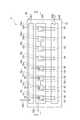
図1は、一実施形態に係る半導体装置の構成を模式的に示す図面である。図1は、半導体装置を半導体チップが搭載されている側から見た場合の構成を模式的に示している。図2は、図1のII−II線に沿った断面構成を模式的に示す図面である。 FIG. 1 is a drawing schematically showing a configuration of a semiconductor device according to an embodiment. FIG. 1 schematically shows a configuration of a semiconductor device as viewed from the side on which a semiconductor chip is mounted. FIG. 2 is a drawing schematically showing a cross-sectional configuration along the line II-II in FIG.
図1に示した半導体装置1は、第1〜第N(Nは2以上の整数)のトランジスタ(第1の半導体チップ)101〜10Nと、第1〜第Nのダイオード(第2の半導体チップ)201〜20Nと、第1〜第Nのトランジスタ101〜10N及び第1〜第Nのダイオード201〜20Nが搭載される回路基板30とを備える。以下の説明では、第1〜第Nのトランジスタ101〜10Nのうちの任意のトランジスタを第kのトランジスタ10kとも称す。同様に、第1〜第Nのダイオード201〜20Nのうちの任意のダイオードを第iのダイオード20iとも称す。The
一実施形態において、半導体装置1は、第1〜第Nのダイオード201〜20Nの保護のためと共に、防湿のために、第1〜第Nのトランジスタ101〜10N及び第1〜第Nのダイオード201〜20Nが封止されるように、図2に示すように、樹脂40によってモールドされていてもよい。図1では、回路基板30上の構成を示すために樹脂40は省略されている。或いは、半導体装置1は、第1〜第Nのダイオード201〜20Nが搭載された回路基板30を収容するケースを備えてもよい。In one embodiment, the
回路基板30は、絶縁基板31と、絶縁基板31の表面(一面)に形成された3つの配線導体32A,32B,32Cとを有する。配線導体32A〜32Cの各々は、一方向に延在しており、3つの配線導体32A〜32Cは互いに平行である。 The
配線導体(第1の配線導体)32Aの一端には、第1の電極端子部33Aの一端が接続されている。配線導体32Bの一端には、第2の電極端子部(第2の配線導体)33Bの一端が接続されている。第2の電極端子部33Bは、図1に示した形態では、配線導体32A〜32Cの延在方向において、第1の電極端子部33Aと反対側に位置する。配線導体32Cには、第3の電極端子部33Cの一端が接続されている。 One end of the first
第1〜第3の電極端子部33A〜33Cは、半導体装置1を、半導体装置1と異なる他の装置、素子又は回路などに接続するための端子である。図2に示したように、半導体装置1が樹脂40又はケースで閉じられている場合には、第1〜第3の電極端子部33A〜33Cの自由端は、半導体装置1の外側に引き出されている。 The first to third electrode terminal portions 33 </ b> A to 33 </ b> C are terminals for connecting the
配線導体32A,32B,32Cの材料の例は、銅といった金属である。配線導体32A,32B,32Cは絶縁されている。配線導体32A,32B,32Cは、例えば印刷により絶縁基板31上に形成され得る。 An example of the material of the
第kのトランジスタ10kは絶縁型電界効果トランジスタ(MOS−FET)である。ただし、第kのトランジスタ10kは、絶縁ゲート型バイポーラトランジスタ、接合型電界効果トランジスタ、接合型バイポーラトランジスタ又はサイリスタでもよい。第kのトランジスタ10kに採用される半導体の例は、SiC、GaN及びダイヤモンドといったワイドバンドギャップ半導体及びSiを含む。The k-th transistor 10k is an insulated field effect transistor (MOS-FET). However, the k-th transistor 10k may be an insulated gate bipolar transistor, a junction field effect transistor, a junction bipolar transistor, or a thyristor. Examples of semiconductors employed in the kth transistor 10k include wide band gap semiconductors such as SiC, GaN, and diamond, and Si.
第kのトランジスタ10kは、第kのトランジスタ10kに電力を供給するための第1及び第2の電極部11k,12kと、第kのトランジスタ10kの動作を制御する第3の電極部13kとを有する。第kのトランジスタ10kがMOS−FETである形態では、第1の電極部11kはドレインとして機能し、第2の電極部12kは、ソースとして機能し、第3の電極部13kはゲートとして機能する。Transistor 10k of the k-th, first and second electrode portions11 k, 12k for supplying power to the transistor 10k of the k-th, third for controlling the operation of the transistor 10k of the k And an electrode portion13k . In the form in which the k-th transistor 10k is a MOS-FET, the first electrode portion 11k functions as a drain, the second electrode portion 12k functions as a source, and the third electrode portion 13k Acts as a gate.
第kのトランジスタ10kは、導電性の接続部材(例えば、ハンダ)を利用して第1の電極部11kが配線導体32A上に接合されることによって、配線導体32A上に固定される。これにより、第kのトランジスタ10kは、配線導体32Aに電気的に接続される。第2の電極部13kは、ワイヤ50を介して配線導体32Bに接続される。これにより、第kのトランジスタ10kの第2の電極部12kは、配線導体32Bに電気的に接続される。更に、第3の電極部13kは、ワイヤ50を介して、配線導体32Cに電気的に接続される。The kth transistor 10k is fixed on the wiring conductor 32</ b> A by bonding the first electrode portion 11k on the wiring conductor 32</ b> A using a conductive connecting member (for example, solder). Thereby, the k-th transistor 10k is electrically connected to the
第iのダイオード20iの例はショットキーバリアダイオードである。第iのダイオード20iは、第iのダイオード20iに電力を供給する第1及び第2の電極部21i,22iを有する。本実施形態では、第1の電極部21iがカソードとして機能し、第2の電極部22iがアノードとして機能する。第iのダイオード20iに採用される半導体の例は、SiC、GaN及びダイヤモンドといったワイドバンドギャップ半導体及びSiを含む。An example of the i-th diode 20i is a Schottky barrier diode. The i-th diode 20i includes first and second electrode portions 21i and 22i that supply power to the i-th diode 20i . In the present embodiment, the first electrode portion 21i functions as a cathode, and the second electrode portion 22i functions as an anode. Examples of semiconductors employed in the i-th diode 20i include Si, wide band gap semiconductors such as SiC, GaN, and diamond.
第iのダイオード20iは、導電性の接続部材(例えば、ハンダ)を利用して第1の電極部21iが第1の配線導体32A上に接合されることによって、配線導体32A上に固定される。これにより、第iのダイオード20iは、配線導体32Aに電気的に接続される。第2の電極部232は、ワイヤ50を介して配線導体32Bに接続される。これにより、第2の電極部222は、配線導体32Bに電気的に接続される。The i-th diode 20i is fixed on the
上記接続関係では、第1〜第Nのトランジスタ101〜10Nに電流が流れる場合、第1〜第Nのダイオード201〜20Nには電流が流れず、逆に、第1〜第Nのダイオード201〜20Nに電流が流れる場合、第1〜第Nのトランジスタ101〜10Nには電流が流れない。In the connection relation, when a current flows through thefirst toNth transistors 101 to 10N , no current flows through the first to Nth diodes 201 to 20N , and conversely, thefirst toNth transistors When current flows through the diodes 201 to 20N , no current flows through the first to Nth transistors 101 to 10N.
従って、第1〜第Nのトランジスタ101〜10Nに電流が流れる場合には、半導体装置1の等価回路は、第1〜第Nのトランジスタ101〜10Nと、配線導体32A、32Bとから構成される第1の並列回路60によって表され、第1〜第Nのダイオード201〜20Nに電流が流れる場合には、半導体装置1の等価回路は、第1〜第Nのダイオード201〜20Nと、配線導体32A、32Bとから構成される第2の並列回路70によって表される。Accordingly, when a current flows through thefirst toNth transistors 101 to 10N , the equivalent circuit of the
第1及び第2の並列回路60,70を利用して、回路基板30上の第1〜第Nのトランジスタ101〜10Nの配置状態と、第1〜第Nのダイオード201〜20Nの配置状態とについて説明する。The first and second
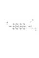
図3は、第1の並列回路を示す図面である。図3は、配線導体32A,32B並びに第1〜第Nのトランジスタ101〜10Nにより構成される第1の並列回路60を、抵抗に着目して模式的に示した回路である。FIG. 3 is a diagram illustrating a first parallel circuit. FIG. 3 is a circuit diagram schematically showing the first
抵抗Rt1〜RtNは、第1〜第Nのトランジスタ101〜10Nのオン抵抗を示す。換言すれば、図3では、抵抗Rt1〜RtNによって、第1〜第Nのトランジスタ101〜10Nを表している。Resistors Rt1 to RtN indicate on-resistances of thefirst toNth transistors 101 to 10N , respectively. In other words, in FIG. 3, thefirst toNth transistors 101 to 10N are represented by resistors Rt1 to RtN.
図3中の抵抗Raは、配線導体32Aにおける第1〜第Nのトランジスタ101〜10Nのうちの隣接するトランジスタ間の抵抗を示す。抵抗Rbは、配線導体32Bにおける第1〜第Nのトランジスタ101〜10Nのうちの隣接するトランジスタ間の抵抗を示す。A resistor Ra in FIG. 3 indicates a resistance between adjacent transistors among thefirst toNth transistors 101 to 10N in the
第1〜第Nのトランジスタ101〜10Nは、図1及び図3では、第1〜第Nのトランジスタ101〜10Nの配列方向において、等間隔に配置されている。そのため、隣接するトランジスタ間の抵抗Raは同じである。ただし、抵抗Raは、導電性を有する配線導体32Aに電流が流れる時に電流が感じる抵抗であるため、微小である。従って、隣接するトランジスタ間の距離が異なっていても、その距離の差によって生じる複数の抵抗Ra間の差は実質的に無視し得る。よって、以下では、隣接するトランジスタ間の抵抗Raは、同じであるとして説明する。隣接するトランジスタ間の抵抗Rbも同じである。以下の説明では、抵抗Ra及び抵抗Rbを配線導体32A,32Bの抵抗とも称す。抵抗Ra及び抵抗Rbは、配線導体32A,32Bの材料が同じであっても、配線導体32A,32Bの幅などが異なっていれば異なる。本実施形態において、抵抗Raと抵抗Rbの大きさは異なる。
図3に示した第1の並列回路60は、第1の並列回路60への電流の入力端61と、第1の並列回路60からの電流の出力端62とを有する。出力端62は、第1の並列回路60のうち第1〜第Nのトランジスタ101〜10Nの配列方向(図3の長手方向)において、入力端61と反対側に位置する。入力端61及び出力端62は、図1に示した半導体装置1の構成では、それぞれ第1の電極端子部33A及び第2の電極端子部33Bに対応する。The first
第1の並列回路60において、抵抗Rt1〜RtNが接続された並行配線は、配線導体32A及び配線導体32Bに対応する。図1に示した第1〜第Nのトランジスタ101〜10Nの接続関係、すなわち、図3に示した第1の並列回路60では、配線導体32A側から配線導体32B側に電流が流れる。従って、第1〜第Nのトランジスタ101〜10Nに対しては配線導体32A及び配線導体32Bのうち、配線導体32Aが第kのトランジスタ10kへの電流供給側の配線導体である。In the first
図4は、第2の並列回路を示す図面である。図4は、配線導体32A,32B並びに第1〜第Nのダイオード201〜20Nにより構成される第2の並列回路70を、抵抗に着目して模式的に示した回路である。抵抗Rd1〜RdNは、第1〜第Nのダイオード201〜20Nのオン抵抗を示す。換言すれば、図4では、抵抗Rd1〜RdNによって、第1〜第Nのダイオード201〜20Nを表している。図4中の抵抗Ra,Rbは、図3の場合と同様に、配線導体32A,32Bの抵抗である。FIG. 4 is a diagram showing a second parallel circuit. FIG. 4 is a circuit diagram schematically showing the second
図4に示した第2の並列回路70は、第2の並列回路70への電流の入力端71と、第2の並列回路70からの電流の出力端72とを有する。出力端72は、第2の並列回路70のうち第1〜第Nのダイオード201〜20Nの配列方向(図4の長手方向)において、入力端71と反対側に位置する。入力端71及び出力端72は、図1に示した半導体装置1の構成では、それぞれ第2の電極端子部33A及び第1の電極端子部33Bに対応する。The second
第2の並列回路70において、抵抗Rd1〜RdNが接続された並行配線は、配線導体32A及び配線導体32Bに対応する。図1に示した第1〜第Nのダイオード201〜20Nの並列接続関係、すなわち、図4に示した第2の並列回路70では、配線導体32B側から配線導体32A側に電流が流れる。従って、第1〜第Nのダイオード201〜20Nに対しては配線導体32A及び配線導体32Bのうち、配線導体32Bが第iのダイオード20iへの電流供給側の配線導体である。In the second
第1〜第Nのトランジスタ101〜10Nは、配線導体32A,32Bそれぞれの抵抗Ra,Rbと第1〜第Nのトランジスタ101〜10Nのオン抵抗とに応じて、第1〜第Nのトランジスタ101〜10Nに均一な電流が流れるように、回路基板30上に配置されている。同様に、第1〜第Nのダイオード201〜20Nは、配線導体32A,32Bそれぞれの抵抗Ra,Rbと第1〜第Nのダイオード201〜20Nのオン抵抗とに応じて、第1〜第Nのダイオード201〜20Nに均一な電流が流れるように、回路基板30上に配置されている。Thefirst toNth transistors 101 to 10N havefirst tofirst transistors according to the resistances Ra and Rb of the
第1〜第Nのトランジスタ101〜10Nの配置順及び第1〜第Nのダイオード201〜20Nの配置順を、抵抗Raが抵抗Rbより大きい場合について説明する。The arrangement order of thefirst toNth transistors 101 to 10N and the arrangement order of the first to Nth diodes 201 to 20N will be described in the case where the resistance Ra is larger than the resistance Rb.
第1の並列回路60において抵抗Raが抵抗Rbより大きい、すなわち、配線導体32Aの抵抗が配線導体32Bの抵抗より大きいことは、第1の並列回路60の並行配線のうち、第1〜第Nのトランジスタ101〜10Nに電流を供給する側の配線(配線導体32A)の抵抗が他方の配線(配線導体32B)の抵抗より大きいことを意味する。この場合、第1〜第Nのトランジスタ101〜10Nは、入力端61側から出力端62に向けて、オン抵抗が小さくなるように配置されている。図1及び図3に示した構成では、第1〜第Nのトランジスタ101,102,103,・・・10Nは、入力端61(第1の電極端子部33A)から出力端62(第2の電極端子部33B)に向けて、第1、第2、第3,・・・,第Nのトランジスタ101,102,103,・・・10Nの順にオン抵抗が小さくなるように配置されている。すなわち、図3に示した第1の並列回路60では、Ra>Rbの場合、入力端61側から出力端62に向けて、Rt1>Rt2>Rt3・・・>RtNである。In the first
一方、第2の並行回路70において抵抗Raが抵抗Rbより大きい、すなわち、配線導体32Aの抵抗が配線導体32Bの抵抗より大きいことは、第2の並列回路70の並行配線のうち、第1〜第Nのダイオード201〜20Nに電流を供給する側の配線(配線導体32B)の抵抗が他方の配線(配線導体32A)の抵抗より小さいことを意味する。この場合、第1〜第Nのダイオード201〜20Nは、入力端71から出力端72に向けて、オン抵抗が大きくなるように配置されている。図1及び図4に示した構成では、第1〜第Nのダイオード201〜20Nは、入力端71(第2の電極端子部33B)から出力端72(第1の電極端子部33A)に向けて、第N,第N−1,・・・,第2,第1のトランジスタ10N,10N−1,・・・101の順にオン抵抗が大きくなるように配置されている。すなわち、図4に示した第2の並列回路70において、Ra>Rbの場合、入力端71から出力端72に向けて、Rd1>Rd2>・・・>RdNである。On the other hand, in the second
次に、第1〜第Nのトランジスタ101〜10Nの配置順及び第1〜第Nのダイオード201〜20Nの配置順を、抵抗Raが抵抗Rbより小さい場合について説明する。Next, the arrangement order of thefirst toNth transistors 101 to 10N and the arrangement order of the first to Nth diodes 201 to 20N will be described in the case where the resistor Ra is smaller than the resistor Rb.
抵抗Raが抵抗Rbより小さい、すなわち、配線導体32Aの抵抗が配線導体32Bの抵抗より小さいことは、第1の並列回路60の並行配線のうち、第1〜第Nのトランジスタ101〜10Nに電流を供給する側の配線(配線導体32A)の抵抗が他方の配線(配線導体32B)の抵抗より小さいことを意味する。この場合、第1〜第Nのトランジスタ101〜10Nは、入力端61側から出力端62に向けて、第1〜第Nのトランジスタ101〜10Nのオン抵抗が大きくなるように配置されている。図1及び図3に示した構成では、第1〜第Nのトランジスタ101,102,103,・・・10Nは、入力端61(第1の電極端子部33A)側から出力端62(第2の電極端子部33B)に向けて、第1、第2、第3,・・・,第Nのトランジスタ101,102,103,・・・10Nの順にオン抵抗が大きくなるように配置されている。すなわち、図3に示した第1の並列回路60において、Ra>Rbの場合、入力端61側から出力端62に向けて、Rt1<Rt2<・・・<RtNである。The fact that the resistance Ra is smaller than the resistance Rb, that is, the resistance of the
一方、第1の並列回路60において抵抗Raが抵抗Rbより小さい、すなわち、配線導体32Aの抵抗が配線導体32Bの抵抗より小さいことは、第2の並列回路70の並行配線のうち、第1〜第Nのダイオード201〜20Nに電流を供給する側の配線(配線導体32B)の抵抗が他方の配線(配線導体32A)の抵抗より大きいことを意味する。この場合、第1〜第Nのダイオード201〜20Nは、入力端71側から出力端72に向けて、第1〜第Nのダイオード201〜20Nのオン抵抗が小さくなるように配置されている。図1及び図4に示した構成では、第1〜第Nのダイオード201,202,203,・・・20Nは、入力端61側から出力端62に向けて、第N,第N−1,・・,第2,第1のダイオード20N,20N−1,・・・,202,201の順にオン抵抗が小さくなるように配置されている。すなわち、図4に示した第2の並列回路70において、Ra<Rbの場合、入力端71側から出力端72に向けて、Rd1<Rd2<・・・<RdNである。On the other hand, in the first
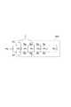
次に、半導体装置1の製造方法について説明する。図5は、半導体装置の製造方法の一例を示すフローチャートである。 Next, a method for manufacturing the
半導体装置1が有する第1〜第Nのトランジスタ101〜10Nのオン抵抗を検査すると共に、第1〜第Nのダイオード201〜20Nのオン抵抗を検査する(検査工程、ステップS10)。検査の仕方は、第1〜第Nのトランジスタ101〜10N及び第1〜第Nのダイオード201〜20Nのオン抵抗を検出できれば特に限定されない。この検査は、第1〜第Nのトランジスタ101〜10N及び第1〜第Nのダイオード201〜20Nを製造した際に通常実施するトランジスタ及びダイオードの試験に対応する。The on-resistances of thefirst toNth transistors 101 to 10N included in the
次に、第1〜第Nのトランジスタ101〜10Nを回路基板30に搭載すると共に、第1〜第Nのダイオード201〜20Nを回路基板30に搭載する(搭載工程、ステップS12)。具体的には、導電性を有する接続部材を介することによって、第kのトランジスタ10kの第1の電極部11k及び第iのダイオード20iの第1の電極部21iを配線導体32A上に固定する。Next, thefirst toNth transistors 101 to 10N are mounted on the
第1〜第Nのトランジスタ101〜10N及び第1〜第Nのダイオード201〜20Nを回路基板30上に搭載する場合には、次のような配置で第1〜第Nのトランジスタ101〜10N及び第1〜第Nのダイオード201〜20Nをそれぞれ回路基板30上に搭載する。When thefirst toNth transistors 101 to 10N and thefirst toNth diodes 201 to 20N are mounted on the
配線導体32Aの抵抗Raが配線導体32Bの抵抗Rbより大きい場合について説明する。 A case where the resistance Ra of the
(第1〜第Nのトランジスタ101〜10Nの配置)
配線導体32A,32Bに第1〜第Nのトランジスタ101〜10Nを並列接続することによって構成されるべき第1の並列回路60において、入力端61から出力端62に向かう方向において、第1〜第Nのトランジスタ101〜10Nのオン抵抗が小さくなるように、第1〜第Nのトランジスタ101〜10Nを回路基板30上に配置する。(Arrangement offirst toNth transistors 101 to 10N )
In the first
(第1〜第Nのダイオード201〜20Nの配置)
配線導体32A,32Bに第1〜第Nのダイオード201〜20Nを並列接続することによって構成されるべき第2の並列回路70において、入力端71から出力端72に向かう方向において、第1〜第Nのダイオード201〜20Nのオン抵抗が大きくなるように、第1〜第Nのダイオード201〜20Nを回路基板30上に配置する。(Arrangement of thefirst to Nth diodes 201 to 20N )
In the second
次に、配線導体32Aの抵抗Raが配線導体32Bの抵抗Rbより小さい場合について説明する。 Next, a case where the resistance Ra of the
(第1〜第Nのトランジスタ101〜10Nの配置)
配線導体32A,32Bに第1〜第Nのトランジスタ101〜10Nを並列接続することによって構成されるべき第1の並列回路60において、入力端61から出力端62に向かう方向において、第1〜第Nのトランジスタ101〜10Nのオン抵抗が大きくなるように、第1〜第Nのトランジスタ101〜10Nを回路基板30上に配置する。(Arrangement offirst toNth transistors 101 to 10N )
In the first
(第1〜第Nのダイオード201〜20Nの配置)
配線導体32A,32Bに第1〜第Nのダイオード201〜20Nを並列接続することによって構成されるべき第2の並列回路70において、入力端71から出力端72に向かう方向において、第1〜第Nのダイオード201〜20Nのオン抵抗が小さくなるように、第1〜第Nのダイオード201〜20Nを回路基板30上に配置する。(Arrangement of thefirst to Nth diodes 201 to 20N )
In the second
その後、第kのトランジスタ10kの第2の電極部12k及び第3の電極部13kをそれぞれ、配線導体32B及び配線導体32Cにワイヤ50を介して接続することによって、第1〜第Nのトランジスタ101〜10Nを並列接続する。同様に、第iのダイオード20iの第2の電極部22iを、配線導体32Bにワイヤ50を利用して接続することによって、第1〜第Nのダイオード201〜20Nを並列接続する(接続工程、ステップS14)。上記配線を施すことによって、第1〜第Nのトランジスタ101〜10Nに着目すると、第1の並列回路60が構成され、第1〜第Nのダイオード201〜20Nに着目すると、第2の並列回路70が構成される。Thereafter, the second electrode portion 12k and the third electrode portion 13k of the k-th transistor 10k are connected to the
ステップS12において、第1の並列回路60の入力端61(又は第2の並列回路70の出力端72)及び第1の並列回路60の出力端62(又は第2の並列回路70の入力端71)の位置は、半導体装置1の設計上の位置(以下、単に「設計位置」と称す)とし得る。この場合、例えば、ステップS14の後で、上記設計位置に合わせて、入力端61及び出力端72として機能する第1の電極端子部33Aと、出力端62及び入力端71として機能する第2の電極端子部33Bを、配線導体32A,32Bに電気的に接続すればよい。 In step S12, the
第1の電極端子部33A及び第2の電極端子部33Bの回路基板30への接続は、ステップS12の工程で行ってもよい。更に、第1の電極端子部33A及び第2の電極端子部33Bが接続された回路基板30を予め準備してもよい。 The connection of the first
一実施形態において、配線導体32A,32Bの抵抗Ra,Rbは、配線導体32A,32Bを構成する材料固有の抵抗値(例えば、単位長さ又は単位断面積当たりの抵抗値)及び配線導体32A,32Bの大きさ(例えば、幅の大きさ)などから理論的に計算し得る場合は、その計算値を用いてもよい。他の実施形態においては、ステップS10又はステップS12において、或いは、ステップS10とステップS12との間において実際に配線導体32A,32Bの抵抗Ra,Rbを測定し、その測定値を利用してもよい。 In one embodiment, the resistances Ra and Rb of the
更に、上述した検査工程、搭載工程及び接続工程のそれぞれにおいて、第1〜第Nのトランジスタ101〜10N及び第1〜第Nのダイオード201〜20Nに対する処理をまとめて説明しているが、第1〜第Nのトランジスタ101〜10Nに対して検査工程、搭載工程及び接続工程を実施し、第1〜第Nのダイオード201〜20Nに対して検査工程、搭載工程及び接続工程を実施してもよい。Furthermore, the processes for thefirst toNth transistors 101 to 10N and thefirst toNth diodes 201 to 20N are collectively described in each of the above-described inspection process, mounting process, and connection process. However, the inspection process, the mounting process, and the connection process are performed on thefirst toNth transistors 101 to 10N , and the inspection process, the mounting process, and the first to Nth diodes 201 to 20N are performed. You may implement a connection process.
図6は、図3に示した第1の並列回路に電力を供給する電力供給部と第1の並列回路との接続形態の一例を示す図面である。図5では電力供給源を直流電源PSとして表している。図5において、直流電源PSの陽極は、入力端61(第1の電極端子部33A)に電気的に接続されており、直流電源PSの陰極は、出力端62(第2の電極端子部33B)に電気的に接続されている。 FIG. 6 is a diagram illustrating an example of a connection form between a power supply unit that supplies power to the first parallel circuit illustrated in FIG. 3 and the first parallel circuit. In FIG. 5, the power supply source is represented as a DC power source PS. In FIG. 5, the anode of the DC power source PS is electrically connected to the input end 61 (first
この構成では、図6に示す矢印αに示す方向に電流が流れる。従って、抵抗Rkに流れる電流、すなわち、第kのトランジスタ10kに流れる電流に作用する(或いは電流が感じる)抵抗の値は、(k−1)×Ra+(N−1―k)×Rb+Rkである。
Ra>Rbである場合、半導体装置1の等価回路である第1の並列回路60では、Rt1>Rt2>・・・>RtNとなるように第1〜第Nのトランジスタ101〜10Nが並べられている。一方、Ra<Rbである場合、第1の並列回路60では、Rt1<Rt2<・・・<RtNとなるように第1〜第Nのトランジスタ101〜10Nが並べられている。そのため、入力端61から出力端62に向けて電流が流れる場合、第1〜第Nのトランジスタ101〜10Nの各々を通して流れる電流の経路において電流に作用する抵抗の値がより等しくなる。その結果、第1〜第Nのトランジスタ101〜10Nに流れる電流の均一化が図られ得る。In this configuration, a current flows in the direction indicated by the arrow α shown in FIG. Accordingly, the value of the resistance that acts on (or feels) the current flowing through the resistor Rk , that is, the current flowing through the k-th transistor 10k is (k−1) × Ra + (N−1−k) × Rb + R.k .
If a ra> Rb, the first
従って、オン抵抗にバラツキのある第1〜第Nのトランジスタ101〜10Nを用いても、第1〜第Nのトランジスタ101〜10Nのうちより小さいオン抵抗を有するトランジスタに、そのトランジスタの電流定格値を超える大きな電流が流れ、トランジスタが破壊されにくい。Therefore, even when thefirst toNth transistors 101 to 10N having variations in on-resistance are used, the transistor having a smaller on-resistance among thefirst toNth transistors 101 to 10N is replaced with the transistor. A large current exceeding the rated current value of the transistor flows, and the transistor is difficult to be destroyed.
第1の並列回路60について説明したが、第2の並列回路70においても同様である。すなわち、第1〜第Nのダイオード201〜20Nのオン抵抗にバラツキが生じていても、第1〜第Nのダイオード201〜20Nのうちより小さいオン抵抗を有するダイオードに、そのダイオードの電流定格値を超える大きな電流が流れ、ダイオードが破壊されにくい。Although the first
従って、半導体装置1を動作させた場合、第1〜第Nのトランジスタ101〜10N及び第1〜第Nのダイオード201〜20Nを有する半導体装置1が壊れにくいので、半導体装置1の信頼性が向上する。Therefore, when the
第1〜第Nのトランジスタ101〜10Nを製造すると、オン抵抗のバラツキが生じ得る。第1〜第Nのダイオード201〜20Nについても同様である。図5を利用して説明した半導体装置の製造方法では、ステップS10において、第1〜第Nのトランジスタ101〜10N及び第1〜第Nのダイオード201〜20Nのオン抵抗を検査している。そして、オン抵抗のバラツキを考慮しながら、配線導体32A,32Bの抵抗と共に、第1〜第Nのトランジスタ101〜10Nのオン抵抗及び第1〜第Nのダイオード201〜20Nのオン抵抗に応じて、例示したように第1〜第Nのトランジスタ101〜10N及び第1〜第Nのダイオード201〜20Nを回路基板30上に配置することによって、半導体装置1を製造している。そのため、第1〜第Nのトランジスタ101〜10Nにより均一な電流が流れると共に、第1〜第Nのダイオード201〜20Nにより均一な電流が流れる半導体装置1が製造される。When thefirst toNth transistors 101 to 10N are manufactured, variations in on-resistance may occur. The same applies to the first to Nth diodes 201 to 20N. In the method for manufacturing a semiconductor device described with reference to FIG. 5, in step S10, the on-resistances of thefirst toNth transistors 101 to 10N and thefirst toNth diodes 201 to 20N are inspected. ing. Then, the ON resistances of thefirst toN-th transistors 101 to 10N and the ON-states of thefirst toN- th diodes 201 to 20N are considered together with the resistances of the
本実施形態では、配線導体32A及び配線導体32Bの抵抗差を利用した。このような抵抗の違いは、配線導体32A及び配線導体32Bに流す電流や、第1〜第Nのトランジスタ101〜10N及び第1〜第Nのダイオード201〜20Nの設置位置に応じて配線導体32A及び配線導体32Bの幅の違いによって生じ得る。しかしながら、オン抵抗のバラツキを考慮して、第1〜第Nのトランジスタ101〜10N及び第1〜第Nのダイオード201〜20Nを、これまで説明したような所定の配置順で配置可能なように、抵抗差を有するように配線導体32A及び配線導体32Bの幅を調整してもよい。配線導体32A及び配線導体32Bの幅は、図1において、配線導体32A又は配線導体32Bの延在方向に直交する方向の長さである。In this embodiment, the resistance difference between the
SiC及びGaNといったワイドバンドギャップ半導体を利用した半導体チップは、現状、製造技術などに起因して電流定格値の小さい小容量品である。そのため、ワイドバンドギャップ半導体チップを利用した半導体装置に大電流を流す場合などには、図1に示したように、複数のトランジスタを並列接続すると共に、複数のダイオードを並列接続する必要が生じる。従って、これまで説明したように、トランジスタ及びダイオードのオン抵抗と配線導体32A,32Bの抵抗とに応じて、複数のトランジスタそれぞれに均一に電流が流れると共に、複数のダイオードそれぞれに均一に電流が流れるような構成は、ワイドバンドギャップ半導体を利用した半導体チップを備えた半導体装置において、特に有効な構成である。 A semiconductor chip using a wide band gap semiconductor such as SiC and GaN is a small-capacity product having a small current rating value at present due to manufacturing technology and the like. Therefore, when a large current is passed through a semiconductor device using a wide band gap semiconductor chip, it is necessary to connect a plurality of transistors in parallel and a plurality of diodes in parallel as shown in FIG. Therefore, as described above, according to the ON resistances of the transistors and diodes and the resistances of the
(第2の実施形態)
図7は、第2の実施形態に係る半導体装置の構成を模式的に示す図面である。半導体装置2は、第2の電極端子部33Bが、配線導体32A〜32Cの延在方向において、第1の電極端子部33Aと同じ側に位置する点で、主に、図1に示した半導体装置1の構成と相違する。この相違点を中心にして半導体装置2について説明する。(Second Embodiment)
FIG. 7 is a drawing schematically showing the configuration of the semiconductor device according to the second embodiment. The
図8は、半導体装置2において、第1〜第Nのトランジスタ101〜10Nと配線導体32A,32Bとで構成される第1の並列回路60Aを示す図面である。図9は、半導体装置2において、第1〜第Nのダイオード201〜20Nと配線導体32A,32Bとで構成される第2の並列回路70Aを示す図面である。図8及び図9に示した回路は、図3及び図4の場合と同様に、抵抗に着目した回路である。FIG. 8 is a diagram illustrating a first
図8に示すように、第1の並列回路60Aの第1〜第Nのトランジスタ101〜10Nの配列方向(図8の長手方向)において、入力端61と出力端62とは、同じ側に位置する。この構成では、第1〜第Nのトランジスタ101〜10Nは、入力端61(又は出力端62)側から反対側に向けて第1〜第Nのトランジスタ101〜10Nのオン抵抗が小さくなるように配置されている。As shown in FIG. 8, the
図8の場合と同様に、図9においても、第2の並列回路70Aの第1〜第Nのダイオード201〜20Nの配列方向(図9の配列方向)において、入力端71と出力端72とは、同じ側に位置する。従って、図8の場合と同様に、第1〜第Nのダイオード201〜20Nは、入力端71(又は出力端72)側から反対側に向けて第1〜第Nのダイオード201〜20Nのオン抵抗が小さくなるように配置されている。As in the case of FIG. 8, also in FIG. 9, the
半導体装置2は、図5に示したステップS12において、第1〜第Nのトランジスタ101〜10N及び第1〜第Nのダイオード201〜20Nの配置順として、図8及び図9を利用して説明した配置順を利用することによって、製造され得る。In step S <b> 12 shown in FIG. 5, the
図10は、電力供給部と、図8に示した回路との接続関係の一例を示す回路図である。図の場合と同様に、図10においても、電力供給部を直流電源PSとして示している。直流電源PSの陽極は、入力端61に接続され、直流電源PSの陰極は出力端62に接続される。 FIG. 10 is a circuit diagram illustrating an example of a connection relationship between the power supply unit and the circuit illustrated in FIG. 8. As in the case of the figure, also in FIG. 10, the power supply unit is shown as a DC power source PS. The anode of the DC power supply PS is connected to the
図10に示した回路では、図10に示す矢印βに示す方向に電流が流れる。抵抗Rt1、すなわち、第1のトランジスタ101を流れる電流に作用する(或いは電流が感じる)抵抗は、抵抗Rt1のみである。一方、例えば、抵抗Rm(mは2〜Nの数)を流れる電流、すなわち、第mのトランジスタ10mを流れる電流に作用する(或いは電流が感じる抵抗)は、(m−1)×Ra+(m−1)×Rb+Rtmである。In the circuit shown in FIG. 10, a current flows in the direction indicated by the arrow β shown in FIG. Resistance Rt1, i.e., acting on the current flowing through the first transistor 101 (or current feel) resistance is only resistance Rt1. On the other hand, for example, the current flowing through the resistor Rm (m is a number from 2 to N), that is, the current flowing through the m-th transistor 10m (or the resistance felt by the current) is (m−1) × Ra + (M−1) × Rb + Rtm .
半導体装置2では、第1の並列回路60Aにおいて、入力端61(又は出力端62)側から反対側に向けて、第1〜第Nのトランジスタ101〜10Nのオン抵抗が小さくなるように、並べられている。そのため、入力端61(又は出力端62)側から反対側にも電流が流れやすい。その結果、第1〜第Nのトランジスタ101〜10Nに流れる電流が均一化され得る。In the
ここでは、第1〜第Nのトランジスタ101〜10Nに電流が流れる場合の半導体装置2の等価回路である第1の並列回路60Aについて説明したが、第2の並列回路70Aについても同様である。すなわち、第2の並列回路70Aにおいても、第1〜第Nのダイオード201〜20Nに流れる電流が均一化され得る。Here, the first
従って、半導体装置2及び半導体装置2の製造方法は、少なくとも第1の実施形態で説明した半導体装置1及び半導体装置1の製造方法の場合と同様の作用効果を有する。半導体装置2の構成では、配線導体32Aと配線導体32Bの抵抗の違いにかかわらず、第1〜第Nのトランジスタ101〜10Nのオン抵抗及び第1〜第Nのダイオード201〜20Nのオン抵抗に基づいて、第1〜第Nのトランジスタ101〜10Nを配置できると共に、第1〜第Nのダイオード201〜20Nの配置できる。そのため、半導体装置2は、その設計が容易である。Accordingly, the
以上、本発明の実施形態について説明したが、本発明は上記実施形態に限定されず、本発明の趣旨を逸脱しない範囲で種々に変更される。 As mentioned above, although embodiment of this invention was described, this invention is not limited to the said embodiment, In the range which does not deviate from the meaning of this invention, it changes variously.
これまでの説明では、第1の半導体チップをトランジスタとして説明し、第2の半導体チップをダイオードとして説明した。しかしながら、これらは説明の便宜のためであり、第1の半導体チップがダイオードであり、第2の半導体チップがトランジスタでもよい。また、第1及び第2の半導体チップは、オン抵抗を有する半導体チップであれば、ダイオード及びトランジスタに限定されない。 In the description so far, the first semiconductor chip has been described as a transistor, and the second semiconductor chip has been described as a diode. However, these are for convenience of explanation, and the first semiconductor chip may be a diode and the second semiconductor chip may be a transistor. The first and second semiconductor chips are not limited to diodes and transistors as long as they are semiconductor chips having on-resistance.
半導体装置は、第1〜第Nのトランジスタ101〜10N及び第1〜第Nのダイオード201〜20Nの一方を備えていればよい。図11は、半導体装置の他の実施形態の模式図である。図11に示した半導体装置3は、第1〜第Nのトランジスタ101〜10Nを備えずに、第1〜第Nのダイオード201〜20Nを備えた半導体装置である。図11では、N=11の場合を示している。The semiconductor device only needs to include one of thefirst toNth transistors 101 to 10N and thefirst toNth diodes 201 to 20N. FIG. 11 is a schematic diagram of another embodiment of a semiconductor device. The
図11に示すように、半導体装置3が有する回路基板30は、配線導体32A,32Bを有していれば、必ずしも配線導体32Cを含まなくてもよい。半導体装置3の抵抗に着目した等価回路は、図4に示した第2の並列回路70に対応する。従って、第1〜第Nのダイオード201〜20Nの配列順は、図1及び図4に示した場合と同様である。As shown in FIG. 11, the
図11に示した半導体装置3は、図1に示した半導体装置で第1〜第Nのトランジスタ101〜10Nを含まない構成に対応する。しかしながら、半導体装置3は、図7に示した半導体装置2において第1〜第Nのトランジスタ101〜10Nを含まない構成であってもよい。更に、半導体装置は、図1及び図7に示した半導体装置1,2において、第1〜第Nのダイオード201〜20Nを備えずに、第1〜第Nのトランジスタ101〜10Nを備える構成であり得る。The
第1〜第Nのトランジスタ101〜10N及び第1〜第Nのダイオード201〜20Nが配線導体32A上に設けられた形態を例示して種々の実施形態を説明した。しかしながら、第1〜第Nのトランジスタ101〜10Nは、回路基板30が有する配線導体32A,32Bを介して第1の並列回路を構成できれば、第1〜第Nのトランジスタ101〜10Nのうち配線導体32B上に設けられていてもよい。第1〜第Nのダイオード201〜20Nについても同様である。Various embodiments have been described by exemplifying an embodiment in which thefirst toNth transistors 101 to 10N and thefirst toNth diodes 201 to 20N are provided on the
更に、第1〜第Nのダイオード201〜20Nが、配線導体32A,32Bを介して並列接続できれば、例えば配線導体32Bは、絶縁基板31において配線導体32Aと形成されている面と反対側の面に形成されていてもよい。第1〜第Nのトランジスタ101〜10Nを半導体装置が備える場合も同様である。Further, if the first to Nth diodes 201 to 20N can be connected in parallel via the
半導体装置1,2では、トランジスタの数とダイオードの数とは同じであったが、それらは異なっていてもよい。半導体装置1,2,3は、半導体装置1,2,3と異なる他の装置及び回路又は素子などの端子が半導体装置1,2,3を使用する際に、配線導体32A,32Bに対して電気的に接続され、配線導体32A,32Bへの電流の入力及び出力が可能であれば、半導体装置1,2,3は、必ずしも第1及び第2の電極端子部33A,33Bを備えなくてもよい。 In the
更に、半導体装置1〜3では、配線導体32A,32Bは一方向に延在しおり、互いに平行であった。しかしながら、第1又は第2の並列回路において、複数の第1の半導体チップ又は複数の第2の半導体チップが例示した配置順に設けられていれば、配線導体32A,32Bの形状等は限定されない。 Furthermore, in the
これまで説明した種々の実施形態及び変形例は互いに組み合わされてもよいし、ある実施形態に他の実施形態又は変形例が適用されてもよい。 Various embodiments and modifications described so far may be combined with each other, and other embodiments or modifications may be applied to a certain embodiment.
1,2,3…半導体装置、101〜10N…第1〜第Nのトランジスタ(複数の第1の半導体チップ)、11k(kは、1〜Nの何れかの数)…第1の電極部(第1の半導体チップの第1の電極部)、12k…第2の電極部(第1の半導体チップの第2の電極部)、201〜20N…第1〜第Nのダイオード(複数の第2の半導体チップ)、21i(iは、1〜Nの何れかの数)…第2の電極部(第2の半導体チップの第1の電極部)、22i…第2の電極部(第2の半導体チップの第1の電極部)、30…回路基板、32A…配線導体(第1の配線導体)、32B…配線導体(第2の配線導体)、60,60A…第1の並列回路、61…入力端(第1の並列回路の入力端)、62…出力端(第1の並列回路の出力端)、70,70A…第2の並列回路、71…入力端(第2の並列回路の入力端)、72…出力端(第2の並列回路の出力端)、Ra…抵抗(第1の配線導体の抵抗)、Rb…抵抗(第2の配線導体の抵抗)。1, 2, 3... Semiconductor device, 101 to 10N ... First to Nth transistors (a plurality of first semiconductor chips), 11k (k is any number from 1 to N). Electrode part (first electrode part of the first semiconductor chip), 12k ... second electrode part (second electrode part of the first semiconductor chip), 201 to 20N ... first to Nth Diodes (a plurality of second semiconductor chips), 21i (i is any number from 1 to N)... Second electrode part (first electrode part of the second semiconductor chip), 22i . Second electrode portion (first electrode portion of second semiconductor chip), 30... Circuit board, 32A... Wiring conductor (first wiring conductor), 32B... Wiring conductor (second wiring conductor), 60. 60A ... first parallel circuit, 61 ... input end (input end of the first parallel circuit), 62 ... output end (output end of the first parallel circuit), 70, 7 0A ... second parallel circuit, 71 ... input end (input end of the second parallel circuit), 72 ... output end (output end of the second parallel circuit), Ra ... resistance (resistance of the first wiring conductor) , Rb... Resistance (resistance of the second wiring conductor).
Claims (11)
Translated fromJapanese前記複数の第1の半導体チップが搭載される回路基板であって、前記複数の第1の半導体チップと電気的に接続される第1及び第2の配線導体を有する、前記回路基板と、
を備え、
前記複数の第1の半導体チップは、前記第1及び第2の配線導体と共に、第1の並列回路を構成するように、並列接続されており、
前記複数の第1の半導体チップに均一な電流が流れるように、前記複数の第1の半導体チップのオン抵抗に応じて、前記複数の第1の半導体チップは前記回路基板上に配置されている、
半導体装置。A plurality of first semiconductor chips;
A circuit board on which the plurality of first semiconductor chips are mounted, the circuit board having first and second wiring conductors electrically connected to the plurality of first semiconductor chips;
With
The plurality of first semiconductor chips are connected in parallel so as to form a first parallel circuit together with the first and second wiring conductors,
The plurality of first semiconductor chips are arranged on the circuit board in accordance with the ON resistance of the plurality of first semiconductor chips so that a uniform current flows through the plurality of first semiconductor chips. ,
Semiconductor device.
前記第1及び第2の配線導体の抵抗は異なっており、
前記第1及び第2の配線導体のうち前記複数の第1の半導体チップへの電流供給側の配線導体の抵抗が他方の配線導体の抵抗より大きい場合、前記第1の並列回路において、前記入力端側から前記出力端側に向けて前記複数の第1の半導体チップのオン抵抗が小さくなっており、
前記第1及び第2の配線導体のうち前記複数の第1の半導体チップへの電流供給側の配線導体の抵抗が他方の配線導体の抵抗より小さい場合、前記第1の並列回路において、前記入力端側から前記出力端側に向けて前記複数の第1の半導体チップのオン抵抗が大きくなっている、
請求項1記載の半導体装置。In the arrangement direction of the plurality of first semiconductor chips in the first parallel circuit, an input end and an output end of a current for the first parallel circuit are opposite to each other,
The resistances of the first and second wiring conductors are different,
In the first parallel circuit, when the resistance of the wiring conductor on the current supply side to the plurality of first semiconductor chips is larger than the resistance of the other wiring conductor among the first and second wiring conductors, On-resistances of the plurality of first semiconductor chips are reduced from the end side toward the output end side,
In the first parallel circuit, when the resistance of the wiring conductor on the current supply side to the plurality of first semiconductor chips is smaller than the resistance of the other wiring conductor among the first and second wiring conductors, On-resistances of the plurality of first semiconductor chips increase from the end side toward the output end side.
The semiconductor device according to claim 1.
前記第1の並列回路において、前記複数の半導体チップのオン抵抗は、前記配列方向において、前記入力端及び前記出力端側と反対側に向けて小さくなっている、
請求項1記載の半導体装置。In the arrangement direction of the plurality of first semiconductor chips in the first parallel circuit, an input end and an output end of a current for the first parallel circuit are on the same side,
In the first parallel circuit, on-resistances of the plurality of semiconductor chips are reduced toward the side opposite to the input end and the output end in the arrangement direction.
The semiconductor device according to claim 1.
請求項1〜3の何れか一項記載の半導体装置。The semiconductor constituting the plurality of first semiconductor chips is a wide band gap semiconductor.
The semiconductor device according to claim 1.
請求項1〜4の何れか一項記載の半導体装置。The first semiconductor chip is a diode or a transistor;
The semiconductor device as described in any one of Claims 1-4.
前記複数の第2の半導体チップは、前記第1及び第2の配線導体と共に、第2の並列回路を構成するように、並列接続されており、
前記複数の第2の半導体チップに均一な電流が流れるように、前記複数の第2の半導体チップのオン抵抗に応じて、前記複数の第2の半導体チップは前記回路基板上に配置されている、
請求項1〜5の何れか一項に記載の半導体装置。A plurality of second semiconductor chips;
The plurality of second semiconductor chips are connected in parallel so as to form a second parallel circuit together with the first and second wiring conductors,
The plurality of second semiconductor chips are arranged on the circuit board in accordance with the on-resistance of the plurality of second semiconductor chips so that a uniform current flows through the plurality of second semiconductor chips. ,
The semiconductor device as described in any one of Claims 1-5.
第1の配線導体と、前記第1の配線導体と絶縁された第2の配線導体とを有する回路基板に、前記複数の第1の半導体チップを搭載する工程と、
前記複数の第1の半導体チップが、前記第1及び第2の配線導体と共に第1の並列回路を構成するように、前記複数の第1の半導体チップを、前記第1及び第2の配線導体を介して並列接続する工程と、
を備え、
前記複数の第1の半導体チップを搭載する工程では、
前記複数の第1の半導体チップに均一な電流が流れるように、前記複数の第1の半導体チップのオン抵抗に応じて、前記複数の第1の半導体チップを前記回路基板上に搭載する、
半導体装置の製造方法。Inspecting on-resistances of a plurality of first semiconductor chips;
Mounting the plurality of first semiconductor chips on a circuit board having a first wiring conductor and a second wiring conductor insulated from the first wiring conductor;
The plurality of first semiconductor chips are connected to the first and second wiring conductors such that the plurality of first semiconductor chips form a first parallel circuit together with the first and second wiring conductors. Connecting in parallel via
With
In the step of mounting the plurality of first semiconductor chips,
The plurality of first semiconductor chips are mounted on the circuit board according to on-resistances of the plurality of first semiconductor chips so that a uniform current flows through the plurality of first semiconductor chips.
A method for manufacturing a semiconductor device.
前記第1及び第2の配線導体の抵抗は異なっており、
前記複数の第1の半導体チップを搭載する工程では、
前記第1及び第2の配線導体のうち前記複数の第1の半導体チップへの電流供給側に位置すべき配線導体の抵抗が他方の配線導体の抵抗より大きい場合、前記入力端側から前記出力端側に向けて前記複数の第1の半導体チップのオン抵抗が小さくなるように、前記複数の第1の半導体チップを前記回路基板上に搭載し、
前記第1及び第2の配線導体のうち前記複数の第1の半導体チップへの電流供給側に位置すべき配線導体の抵抗が他方の配線導体の抵抗より小さい場合、前記入力端側から前記出力端側に向けて前記複数の第1の半導体チップのオン抵抗が大きくなるように、前記複数の第1の半導体チップを前記回路基板上に搭載する、
請求項8記載の半導体装置の製造方法。In the first parallel circuit, an output terminal of current from the first parallel circuit is opposite to an input terminal of current from the first parallel circuit in the arrangement direction of the plurality of first semiconductor chips. The first parallel circuit located,
The resistances of the first and second wiring conductors are different,
In the step of mounting the plurality of first semiconductor chips,
When the resistance of the wiring conductor to be positioned on the current supply side to the plurality of first semiconductor chips among the first and second wiring conductors is larger than the resistance of the other wiring conductor, the output from the input end side The plurality of first semiconductor chips are mounted on the circuit board so that the on-resistance of the plurality of first semiconductor chips decreases toward the end side,
When the resistance of the wiring conductor to be positioned on the current supply side to the plurality of first semiconductor chips among the first and second wiring conductors is smaller than the resistance of the other wiring conductor, the output from the input end side Mounting the plurality of first semiconductor chips on the circuit board so that the on-resistance of the plurality of first semiconductor chips increases toward the end side;
A method for manufacturing a semiconductor device according to claim 8.
前記複数の第1の半導体チップを前記回路基板に搭載する工程では、前記配列方向において、前記入力端及び前記出力端側と反対側に向けて、前記複数の第1の半導体チップのオン抵抗が小さくなるように、前記複数の第1の半導体チップを前記回路基板上に搭載する、
請求項8記載の半導体装置の製造方法。In the first parallel circuit, the current input terminal to the first parallel circuit and the current output terminal from the first parallel circuit are on the same side in the arrangement direction of the plurality of first semiconductor chips. A parallel circuit in
In the step of mounting the plurality of first semiconductor chips on the circuit board, on-resistances of the plurality of first semiconductor chips are directed toward the side opposite to the input end and the output end in the arrangement direction. Mounting the plurality of first semiconductor chips on the circuit board so as to be smaller;
A method for manufacturing a semiconductor device according to claim 8.
前記複数の第2の半導体チップを前記回路基板上に搭載する工程と、
前記第1及び第2の配線導体と共に第2の並列回路を構成するように、前記複数の第2の半導体チップを、前記第1及び第2の配線導体を介して並列接続する工程と、
を更に備え、
前記複数の第2の半導体チップを前記回路基板上に搭載する工程では、前記複数の第2の半導体チップに均一な電流が流れるように、前記複数の第2の半導体チップのオン抵抗に応じて、前記複数の第2の半導体チップを前記回路基板上に搭載する、
請求項8〜10の何れか一項記載の半導体装置の製造方法。Further testing the on-resistance of the plurality of second semiconductor chips;
Mounting the plurality of second semiconductor chips on the circuit board;
Connecting the plurality of second semiconductor chips in parallel via the first and second wiring conductors so as to form a second parallel circuit together with the first and second wiring conductors;
Further comprising
In the step of mounting the plurality of second semiconductor chips on the circuit board, according to on-resistances of the plurality of second semiconductor chips so that a uniform current flows through the plurality of second semiconductor chips. Mounting the plurality of second semiconductor chips on the circuit board;
The method for manufacturing a semiconductor device according to claim 8.
Priority Applications (5)
| Application Number | Priority Date | Filing Date | Title |
|---|---|---|---|
| JP2012145086AJP5939055B2 (en) | 2012-06-28 | 2012-06-28 | Semiconductor device and manufacturing method of semiconductor device |
| EP13810696.8AEP2869341A1 (en) | 2012-06-28 | 2013-05-16 | Semiconductor device and semiconductor device manufacturing method |
| CN201380028421.9ACN104350596B (en) | 2012-06-28 | 2013-05-16 | Semiconductor device and semiconductor device manufacturing method |
| PCT/JP2013/063708WO2014002637A1 (en) | 2012-06-28 | 2013-05-16 | Semiconductor device and semiconductor device manufacturing method |
| US13/902,180US8928002B2 (en) | 2012-06-28 | 2013-05-24 | Semiconductor device and method of manufacturing semiconductor device |
Applications Claiming Priority (1)
| Application Number | Priority Date | Filing Date | Title |
|---|---|---|---|
| JP2012145086AJP5939055B2 (en) | 2012-06-28 | 2012-06-28 | Semiconductor device and manufacturing method of semiconductor device |
Publications (2)
| Publication Number | Publication Date |
|---|---|
| JP2014011225A JP2014011225A (en) | 2014-01-20 |
| JP5939055B2true JP5939055B2 (en) | 2016-06-22 |
Family
ID=49777176
Family Applications (1)
| Application Number | Title | Priority Date | Filing Date |
|---|---|---|---|
| JP2012145086AActiveJP5939055B2 (en) | 2012-06-28 | 2012-06-28 | Semiconductor device and manufacturing method of semiconductor device |
Country Status (5)
| Country | Link |
|---|---|
| US (1) | US8928002B2 (en) |
| EP (1) | EP2869341A1 (en) |
| JP (1) | JP5939055B2 (en) |
| CN (1) | CN104350596B (en) |
| WO (1) | WO2014002637A1 (en) |
Families Citing this family (5)
| Publication number | Priority date | Publication date | Assignee | Title |
|---|---|---|---|---|
| EP3582598B1 (en)* | 2014-01-30 | 2024-07-24 | Wolfspeed, Inc. | Low profile, highly configurable, current sharing paralleled wide band gap power device power module |
| JP6672908B2 (en)* | 2016-03-10 | 2020-03-25 | 富士電機株式会社 | Semiconductor device and method of manufacturing semiconductor device |
| US10222307B2 (en) | 2016-05-18 | 2019-03-05 | Credo Biomedical Pte Ltd. | Mixing and transfer device for materials used in biological and biochemical assays |
| JP7447480B2 (en)* | 2019-12-23 | 2024-03-12 | 富士電機株式会社 | Electronic circuits, semiconductor modules and semiconductor devices |
| JP7622835B2 (en)* | 2021-06-04 | 2025-01-28 | 富士電機株式会社 | Semiconductor Device |
Family Cites Families (16)
| Publication number | Priority date | Publication date | Assignee | Title |
|---|---|---|---|---|
| JPH085564Y2 (en)* | 1986-09-30 | 1996-02-14 | 日本輸送機株式会社 | Transistor parallel connection device |
| JPH098280A (en)* | 1995-06-15 | 1997-01-10 | Hitachi Ltd | Semiconductor device and inverter device using the same |
| JP2000311983A (en)* | 1999-04-28 | 2000-11-07 | Mitsubishi Electric Corp | Power semiconductor module |
| JP2001308264A (en)* | 2000-04-21 | 2001-11-02 | Toyota Industries Corp | Semiconductor device |
| JP2003060157A (en)* | 2001-08-08 | 2003-02-28 | Mitsubishi Electric Corp | Power module |
| JP2004095670A (en) | 2002-08-29 | 2004-03-25 | Toshiba Corp | Semiconductor device |
| ATE500616T1 (en)* | 2002-08-29 | 2011-03-15 | Seoul Semiconductor Co Ltd | LIGHT EMITTING COMPONENT WITH LIGHT EMITTING DIODES |
| JP2006066845A (en)* | 2004-07-29 | 2006-03-09 | Seiko Epson Corp | Surface emitting wafer, method for manufacturing the same, and burn-in method for surface emitting wafer |
| KR100616415B1 (en)* | 2005-08-08 | 2006-08-29 | 서울옵토디바이스주식회사 | AC light emitting device |
| WO2008038910A1 (en)* | 2006-09-25 | 2008-04-03 | Seoul Opto Device Co., Ltd. | Light emitting diode having alingap active layer and method of fabricating the same |
| JP4830877B2 (en)* | 2007-01-31 | 2011-12-07 | トヨタ自動車株式会社 | Manufacturing method of semiconductor device |
| KR101665932B1 (en)* | 2010-02-27 | 2016-10-13 | 삼성전자주식회사 | Semiconductor light emitting device having a multi-cell array, light emitting module and illumination apparatus |
| JP5174085B2 (en)* | 2010-05-20 | 2013-04-03 | 三菱電機株式会社 | Semiconductor device |
| JP2011254021A (en)* | 2010-06-03 | 2011-12-15 | Sumitomo Electric Ind Ltd | Method of manufacturing semiconductor device |
| TW201318147A (en)* | 2011-10-26 | 2013-05-01 | Phostek Inc | Light-emitting diode array |
| WO2013179547A1 (en)* | 2012-06-01 | 2013-12-05 | パナソニック株式会社 | Power semiconductor device |
- 2012
- 2012-06-28JPJP2012145086Apatent/JP5939055B2/enactiveActive
- 2013
- 2013-05-16CNCN201380028421.9Apatent/CN104350596B/enactiveActive
- 2013-05-16WOPCT/JP2013/063708patent/WO2014002637A1/enactiveApplication Filing
- 2013-05-16EPEP13810696.8Apatent/EP2869341A1/ennot_activeWithdrawn
- 2013-05-24USUS13/902,180patent/US8928002B2/enactiveActive
Also Published As
| Publication number | Publication date |
|---|---|
| US8928002B2 (en) | 2015-01-06 |
| EP2869341A4 (en) | 2015-05-06 |
| JP2014011225A (en) | 2014-01-20 |
| EP2869341A1 (en) | 2015-05-06 |
| US20140001482A1 (en) | 2014-01-02 |
| CN104350596A (en) | 2015-02-11 |
| CN104350596B (en) | 2017-08-08 |
| WO2014002637A1 (en) | 2014-01-03 |
Similar Documents
| Publication | Publication Date | Title |
|---|---|---|
| CN102364345B (en) | Circuit arrangement with shunt resistor and semiconductor module with corresponding power | |
| JP5939055B2 (en) | Semiconductor device and manufacturing method of semiconductor device | |
| US11346879B2 (en) | Semiconductor device | |
| JP2011199162A (en) | Semiconductor device | |
| CN110176446B (en) | Semiconductor device with a semiconductor device having a plurality of semiconductor chips | |
| CN101252129A (en) | Semiconductor device | |
| JP6352200B2 (en) | Semiconductor device | |
| US11195783B2 (en) | Semiconductor device | |
| JP2020013955A (en) | Semiconductor device and resistance element | |
| JP5494851B2 (en) | Semiconductor device | |
| US10056175B2 (en) | Thermistor mounting apparatus and thermistor component | |
| JP2005142189A (en) | Semiconductor device | |
| CN104934398A (en) | Electronic Component And Leadframe | |
| US11029339B2 (en) | Current measuring apparatus | |
| CN109564918B (en) | Semiconductor device with a semiconductor device having a plurality of semiconductor chips | |
| JP2010251551A (en) | Electronic circuit board and power semiconductor module | |
| CN115117040B (en) | Semiconductor device with a semiconductor device having a plurality of semiconductor chips | |
| US20130126866A1 (en) | Semiconductor device and manufacturing method thereof | |
| CN107861056A (en) | It is determined that the method and system and power switch circuit of the electric current for passing through power switch | |
| KR20170090135A (en) | Inverter package | |
| JP2001358283A (en) | Current shunt and composite semiconductor device comprising it | |
| JP2016092100A (en) | Semiconductor device | |
| US11881524B2 (en) | Semiconductor device | |
| US20240387473A1 (en) | Semiconductor module | |
| CN117439584A (en) | Input/output port circuit and its chip |
Legal Events
| Date | Code | Title | Description |
|---|---|---|---|
| A621 | Written request for application examination | Free format text:JAPANESE INTERMEDIATE CODE: A621 Effective date:20150324 | |
| TRDD | Decision of grant or rejection written | ||
| A01 | Written decision to grant a patent or to grant a registration (utility model) | Free format text:JAPANESE INTERMEDIATE CODE: A01 Effective date:20160419 | |
| A61 | First payment of annual fees (during grant procedure) | Free format text:JAPANESE INTERMEDIATE CODE: A61 Effective date:20160502 | |
| R150 | Certificate of patent or registration of utility model | Ref document number:5939055 Country of ref document:JP Free format text:JAPANESE INTERMEDIATE CODE: R150 | |
| R250 | Receipt of annual fees | Free format text:JAPANESE INTERMEDIATE CODE: R250 | |
| R250 | Receipt of annual fees | Free format text:JAPANESE INTERMEDIATE CODE: R250 | |
| R250 | Receipt of annual fees | Free format text:JAPANESE INTERMEDIATE CODE: R250 | |
| R250 | Receipt of annual fees | Free format text:JAPANESE INTERMEDIATE CODE: R250 | |
| R250 | Receipt of annual fees | Free format text:JAPANESE INTERMEDIATE CODE: R250 | |
| R250 | Receipt of annual fees | Free format text:JAPANESE INTERMEDIATE CODE: R250 | |
| R250 | Receipt of annual fees | Free format text:JAPANESE INTERMEDIATE CODE: R250 |