JP5926286B2 - Electronic devices containing pyrimidine compounds - Google Patents
Electronic devices containing pyrimidine compoundsDownload PDFInfo
- Publication number
- JP5926286B2 JP5926286B2JP2013546348AJP2013546348AJP5926286B2JP 5926286 B2JP5926286 B2JP 5926286B2JP 2013546348 AJP2013546348 AJP 2013546348AJP 2013546348 AJP2013546348 AJP 2013546348AJP 5926286 B2JP5926286 B2JP 5926286B2
- Authority
- JP
- Japan
- Prior art keywords
- compound
- layer
- formula
- pyrimidine
- photoactive
- Prior art date
- Legal status (The legal status is an assumption and is not a legal conclusion. Google has not performed a legal analysis and makes no representation as to the accuracy of the status listed.)
- Active
Links
- 0*c1c(*)nc(*)nc1*Chemical compound*c1c(*)nc(*)nc1*0.000description1
- XSKOWNIVPOWBMD-YVJQMWMVSA-NC/C=N\C=C(/C=C)\c1cc(-c2nc(C(C3)=CC=CC3c3cncnc3)cc(-c3cccc(-c4ccccc4)c3)n2)ccc1Chemical compoundC/C=N\C=C(/C=C)\c1cc(-c2nc(C(C3)=CC=CC3c3cncnc3)cc(-c3cccc(-c4ccccc4)c3)n2)ccc1XSKOWNIVPOWBMD-YVJQMWMVSA-N0.000description1
- XMSNIJYZAJOFFG-UHFFFAOYSA-Nc(cc1)ccc1-c1cccc(-c2c(-c3cccc(-c4cncnc4)c3)nc(-c3cccc(-c4ccccc4)c3)nc2-c2cc(-c3cncnc3)ccc2)c1Chemical compoundc(cc1)ccc1-c1cccc(-c2c(-c3cccc(-c4cncnc4)c3)nc(-c3cccc(-c4ccccc4)c3)nc2-c2cc(-c3cncnc3)ccc2)c1XMSNIJYZAJOFFG-UHFFFAOYSA-N0.000description1
Images


Classifications
- C—CHEMISTRY; METALLURGY
- C07—ORGANIC CHEMISTRY
- C07D—HETEROCYCLIC COMPOUNDS
- C07D239/00—Heterocyclic compounds containing 1,3-diazine or hydrogenated 1,3-diazine rings
- C07D239/02—Heterocyclic compounds containing 1,3-diazine or hydrogenated 1,3-diazine rings not condensed with other rings
- C07D239/24—Heterocyclic compounds containing 1,3-diazine or hydrogenated 1,3-diazine rings not condensed with other rings having three or more double bonds between ring members or between ring members and non-ring members
- C07D239/26—Heterocyclic compounds containing 1,3-diazine or hydrogenated 1,3-diazine rings not condensed with other rings having three or more double bonds between ring members or between ring members and non-ring members with only hydrogen atoms, hydrocarbon or substituted hydrocarbon radicals, directly attached to ring carbon atoms
- C—CHEMISTRY; METALLURGY
- C07—ORGANIC CHEMISTRY
- C07D—HETEROCYCLIC COMPOUNDS
- C07D401/00—Heterocyclic compounds containing two or more hetero rings, having nitrogen atoms as the only ring hetero atoms, at least one ring being a six-membered ring with only one nitrogen atom
- C07D401/02—Heterocyclic compounds containing two or more hetero rings, having nitrogen atoms as the only ring hetero atoms, at least one ring being a six-membered ring with only one nitrogen atom containing two hetero rings
- C07D401/10—Heterocyclic compounds containing two or more hetero rings, having nitrogen atoms as the only ring hetero atoms, at least one ring being a six-membered ring with only one nitrogen atom containing two hetero rings linked by a carbon chain containing aromatic rings
- C—CHEMISTRY; METALLURGY
- C07—ORGANIC CHEMISTRY
- C07D—HETEROCYCLIC COMPOUNDS
- C07D401/00—Heterocyclic compounds containing two or more hetero rings, having nitrogen atoms as the only ring hetero atoms, at least one ring being a six-membered ring with only one nitrogen atom
- C07D401/14—Heterocyclic compounds containing two or more hetero rings, having nitrogen atoms as the only ring hetero atoms, at least one ring being a six-membered ring with only one nitrogen atom containing three or more hetero rings
- C—CHEMISTRY; METALLURGY
- C09—DYES; PAINTS; POLISHES; NATURAL RESINS; ADHESIVES; COMPOSITIONS NOT OTHERWISE PROVIDED FOR; APPLICATIONS OF MATERIALS NOT OTHERWISE PROVIDED FOR
- C09K—MATERIALS FOR MISCELLANEOUS APPLICATIONS, NOT PROVIDED FOR ELSEWHERE
- C09K11/00—Luminescent, e.g. electroluminescent, chemiluminescent materials
- C09K11/06—Luminescent, e.g. electroluminescent, chemiluminescent materials containing organic luminescent materials
- H—ELECTRICITY
- H10—SEMICONDUCTOR DEVICES; ELECTRIC SOLID-STATE DEVICES NOT OTHERWISE PROVIDED FOR
- H10K—ORGANIC ELECTRIC SOLID-STATE DEVICES
- H10K10/00—Organic devices specially adapted for rectifying, amplifying, oscillating or switching; Organic capacitors or resistors having potential barriers
- H10K10/40—Organic transistors
- H10K10/46—Field-effect transistors, e.g. organic thin-film transistors [OTFT]
- H10K10/462—Insulated gate field-effect transistors [IGFETs]
- H10K10/464—Lateral top-gate IGFETs comprising only a single gate
- H—ELECTRICITY
- H10—SEMICONDUCTOR DEVICES; ELECTRIC SOLID-STATE DEVICES NOT OTHERWISE PROVIDED FOR
- H10K—ORGANIC ELECTRIC SOLID-STATE DEVICES
- H10K85/00—Organic materials used in the body or electrodes of devices covered by this subclass
- H10K85/60—Organic compounds having low molecular weight
- H10K85/649—Aromatic compounds comprising a hetero atom
- H10K85/654—Aromatic compounds comprising a hetero atom comprising only nitrogen as heteroatom
- H—ELECTRICITY
- H01—ELECTRIC ELEMENTS
- H01L—SEMICONDUCTOR DEVICES NOT COVERED BY CLASS H10
- H01L2924/00—Indexing scheme for arrangements or methods for connecting or disconnecting semiconductor or solid-state bodies as covered by H01L24/00
- H01L2924/10—Details of semiconductor or other solid state devices to be connected
- H01L2924/11—Device type
- H01L2924/13—Discrete devices, e.g. 3 terminal devices
- H01L2924/1304—Transistor
- H01L2924/1306—Field-effect transistor [FET]
- H01L2924/1307—Organic Field-Effect Transistor [OFET]
Landscapes
- Chemical & Material Sciences (AREA)
- Organic Chemistry (AREA)
- Engineering & Computer Science (AREA)
- Materials Engineering (AREA)
- Physics & Mathematics (AREA)
- Spectroscopy & Molecular Physics (AREA)
- Electroluminescent Light Sources (AREA)
- Plural Heterocyclic Compounds (AREA)
Description
Translated fromJapanese関連出願
本出願は、米国特許法第119条(e)に基づき、その記載内容全体が参照により援用される2010年12月21日に出願された米国仮特許出願第61/425,556号明細書の優先権を主張する。RELATED APPLICATIONS This application is based on US Provisional Patent Application No. 61 / 425,556 filed on Dec. 21, 2010, which is incorporated by reference in its entirety, under 35 USC 119 (e). Claim the priority of the book.
本開示は、一般に電気活性ピリミジン化合物に関する。これはまた、ピリミジン化合物を有する少なくとも1層を含む有機電子デバイスにも関する。 The present disclosure relates generally to electroactive pyrimidine compounds. This also relates to an organic electronic device comprising at least one layer having a pyrimidine compound.
OLEDディスプレイを構成する有機発光ダイオード(「OLED」)などの有機電子デバイスにおいて、有機電気活性層は、OLEDディスプレイ中で2層の電気接触層の間に挟まれている。OLED中、電気接触層の間に電圧が印加された時に、有機光活性層は、光透過性電気接触層を透過する光を発する。 In organic electronic devices such as organic light emitting diodes (“OLED”) that make up OLED displays, an organic electroactive layer is sandwiched between two electrical contact layers in the OLED display. In the OLED, when a voltage is applied between the electrical contact layers, the organic photoactive layer emits light that is transmitted through the light transmissive electrical contact layer.
発光ダイオード中の電気活性成分として有機エレクトロルミネッセント化合物が使用されることは周知である。単純な有機分子、共役ポリマー、および有機金属錯体が使用されている。 It is well known that organic electroluminescent compounds are used as electroactive components in light emitting diodes. Simple organic molecules, conjugated polymers, and organometallic complexes have been used.
光活性材料を使用するデバイスは、多くの場合、光活性(例えば発光)層と接触層(正孔注入接触層)との間に配置された1層またはそれ以上の電荷輸送層を含む。デバイスは2層以上の接触層を含むことができる。光活性層と正孔注入接触層との間に正孔輸送層を配置することができる。正孔注入接触層はアノードと呼ばれてもよい。光活性層と電子注入接触層との間に電子輸送層を配置することができる。電子注入接触層はカソードと呼ばれてもよい。電荷輸送材料は、光活性材料と組み合わせてホストとして使用することもできる。 Devices that use photoactive materials often include one or more charge transport layers disposed between a photoactive (eg, light emitting) layer and a contact layer (hole-injecting contact layer). The device can include two or more contact layers. A hole transport layer can be disposed between the photoactive layer and the hole injection contact layer. The hole injection contact layer may be referred to as the anode. An electron transport layer can be disposed between the photoactive layer and the electron injecting contact layer. The electron injection contact layer may be referred to as the cathode. The charge transport material can also be used as a host in combination with a photoactive material.
電子デバイスのための新規材料が引き続き必要とされている。 There is a continuing need for new materials for electronic devices.
式Iまたは式II Formula I or Formula II

(式中、
R1〜R4は、同一であるか、または異なって、H、D、アルキル、シリル、アルコキシ、シアノまたはアリールであり、R1〜R4の少なくとも2つはアリール基であり、かつアリール基の少なくとも1つはN,O,S−複素環を含むが、ただし、R1〜R4の2つがN−カルバゾリル基を含む場合、R1〜R4の2つはアリールではない)(Where
R1 to R4 are the same or different and are H, D, alkyl, silyl, alkoxy, cyano or aryl, at least two of R1 to R4 are aryl groups, and aryl groups at least one N, O, including S- heterocyclic,however, if it contains two of N- carbazolyl group R 1 to R4, two of R 1 to R4 is not aryl)
(式中、
Qは、単結合または炭化水素アリールであり、かつ
R5およびR6は、それぞれ、同一であるか、または異なって、H、D、アルキル、シリル、アルコキシ、シアノまたはアリールであり、R5の少なくとも1つおよび少なくともR6の1つはアリール基であり、かつアリール基の少なくとも1つはN,O,S−複素環を含む)を有するピリミジン化合物が提供される。(Where
Q is a single bond or a hydrocarbon aryl, and R5 and R6 are the same or different and are each H, D, alkyl, silyl, alkoxy, cyano or aryl, and R5 There is provided a pyrimidine compound having at least one and at least one of R6 is an aryl group, and at least one of the aryl groups comprises an N, O, S-heterocycle.
(a)式Iまたは式IIを有するピリミジン化合物であるホストと、(b)380〜750nmで発光極大を有するエレクトロルミネセンスが可能なドーパントとを含んでなる組成物も提供される。 Also provided is a composition comprising (a) a host that is a pyrimidine compound having Formula I or Formula II, and (b) a dopant capable of electroluminescence having an emission maximum at 380-750 nm.
式Iまたは式IIの化合物を含んでなる少なくとも1層を含んでなる電子デバイスも提供される。 There is also provided an electronic device comprising at least one layer comprising a compound of formula I or formula II.
基板と、
絶縁層と、
ゲート電極と、
ソース電極と、
ドレイン電極と、
式Iまたは式IIを有するピリミジン化合物を含んでなる有機半導体層と
を含んでなる薄膜トランジスタであって、ゲート電極および半導体層が両方とも絶縁層と接触し、ソース電極およびドレイン電極が両方とも半導体層と接触し、そして電極が互いに接触しない条件の任意の配列において、絶縁層、ゲート電極、半導体層、ソース電極およびドレイン電極を配置することができる、薄膜トランジスタも提供される。A substrate,
An insulating layer;
A gate electrode;
A source electrode;
A drain electrode;
A thin film transistor comprising an organic semiconductor layer comprising a pyrimidine compound having formula I or formula II, wherein both the gate electrode and the semiconductor layer are in contact with the insulating layer, and both the source electrode and the drain electrode are semiconductor layers Also provided is a thin film transistor in which an insulating layer, a gate electrode, a semiconductor layer, a source electrode and a drain electrode can be disposed in any arrangement that is in contact with each other and the electrodes are not in contact with each other.
また、2層の電気接触層の間に配置された少なくとも1層の電気活性層を含んでなり、デバイスの少なくとも1層の電気活性層が式Iまたは式IIを有するピリミジン化合物を含む電子デバイスも提供される。 There is also an electronic device comprising at least one electroactive layer disposed between two electrical contact layers, wherein at least one electroactive layer of the device comprises a pyrimidine compound having formula I or formula II. Provided.
また、アノードと、正孔注入層と、光活性層と、電子輸送層と、カソードとを含んでなる有機電子デバイスであって、光活性層および電子輸送層の少なくとも1層が式Iまたは式IIを有する化合物を含んでなる有機電子デバイスも提供される。 An organic electronic device comprising an anode, a hole injection layer, a photoactive layer, an electron transport layer, and a cathode, wherein at least one of the photoactive layer and the electron transport layer is represented by Formula I or Formula An organic electronic device comprising a compound having II is also provided.
以上の一般的説明および以下の詳細な説明は、単に例示的および説明的なものであり、添付の特許請求の範囲に定義される本発明を限定するものではない。 The foregoing general description and the following detailed description are exemplary and explanatory only and are not restrictive of the invention, as defined in the appended claims.
本明細書において提示される概念の理解を深めるために、添付の図面に実施形態を説明する。 In order to better understand the concepts presented herein, embodiments are described in the accompanying drawings.
当業者は、図面中の物体が、平易かつ明快にするために示されており、必ずしも縮尺通りに描かれているわけではないことを認識する。例えば、実施形態の理解を高めるために、図面中の一部の物体の寸法が他の物体よりも誇張されていてもよい。 Those skilled in the art recognize that the objects in the drawings are shown for simplicity and clarity and have not necessarily been drawn to scale. For example, in order to enhance the understanding of the embodiment, the dimensions of some objects in the drawings may be exaggerated more than other objects.
多くの態様および実施形態を以上に説明しているが、これらは単に例示的で非限定的なものである。本明細書を読めば、本発明の範囲から逸脱することなく他の態様および実施形態が可能であることは当業者に認識される。 Many aspects and embodiments have been described above and are merely exemplary and not limiting. After reading this specification, skilled artisans will recognize that other aspects and embodiments are possible without departing from the scope of the invention.
いずれか1つ以上の実施形態のその他の特徴および利点は、以下の詳細な説明および特許請求の範囲から明らかとなるであろう。詳細な説明では、最初に用語の定義および説明を記載し、続いてピリミジン化合物、電気活性組成物、電子デバイス、そして最後に実施例を記載する。 Other features and advantages of any one or more embodiments will be apparent from the following detailed description and from the claims. In the detailed description, definitions and explanations of terms are given first, followed by pyrimidine compounds, electroactive compositions, electronic devices, and finally examples.
1.用語の定義および説明
以下に記載される実施形態の詳細を記載する前に、一部の用語について定義または説明を行う。1. Definitions and Explanations of Terms Before describing the details of the embodiments described below, some terms are defined or explained.
用語「アルキル」は、脂肪族炭化水素から誘導される基を意味することが意図される。 The term “alkyl” is intended to mean a group derived from an aliphatic hydrocarbon.
用語「アリール」は、芳香族炭化水素から誘導される基を意味することが意図される。用語「芳香族化合物」は、非局在化パイ電子を有する少なくとも1個の不飽和環式基を含んでなる有機化合物を意味することが意図される。この用語は、炭素および水素原子のみを有する芳香族化合物、ならびに環式基中の炭素原子の1個またはそれ以上が、窒素、酸素、硫黄などの別の原子によって置き換えられる複素環式芳香族化合物を包含することが意図される。 The term “aryl” is intended to mean a group derived from an aromatic hydrocarbon. The term “aromatic compound” is intended to mean an organic compound comprising at least one unsaturated cyclic group having delocalized pi electrons. The term includes aromatic compounds having only carbon and hydrogen atoms, and heterocyclic aromatic compounds in which one or more of the carbon atoms in the cyclic group is replaced by another atom such as nitrogen, oxygen, sulfur, etc. Is intended to be included.
用語「カルバゾリル」は、以下の単位 The term “carbazolyl” means the unit
(式中、Rは、H、D、アルキル、アリールまたは結合点であり、かつYは、アリールまたは結合点である)を含有する基を指す。用語N−カルバゾリルは、Yが結合点であるカルバゾリル基を指す。Wherein R is H, D, alkyl, aryl or a point of attachment, and Y is an aryl or point of attachment. The term N-carbazolyl refers to a carbazolyl group where Y is the point of attachment.
層、材料、部材、または構造に関して言及される場合、用語「電荷輸送」は、そのような層、材料、部材、または構造が、比較的効率的かつ少ない電荷損失で、そのような層、材料、部材、または構造の厚さを通過するそのような電荷の移動を促進することを意味することを意図している。正孔輸送材料は正電荷を促進し;電子輸送材料は負電荷を促進する。光活性材料も、ある程度の電荷輸送特性を有し得るが、用語「電荷輸送層、材料、部材、または構造」は、主要な機能が発光または光受容である層、材料、部材、または構造を含むことが意図されない。 When referred to in reference to a layer, material, member, or structure, the term “charge transport” refers to such layer, material, member, or structure such that the layer, material, member, or structure is relatively efficient and with low charge loss. It is intended to mean that it facilitates the movement of such charges through the thickness of the member, or structure. Hole transport materials promote positive charges; electron transport materials promote negative charges. Although photoactive materials may also have some charge transport properties, the term “charge transport layer, material, member, or structure” refers to a layer, material, member, or structure whose primary function is light emission or light reception. Not intended to be included.
用語「ドーパント」は、ホスト材料を含む層中で、そのような材料を含まない場合の層の放射線放出の電子的特徴または波長、受容、またはフィルタリングと比較して、層の放射線放出の電子的特徴または標的波長、受容、またはフィルタリングを変化させる材料を意味することが意図される。 The term “dopant” refers to a layer's radiation emitting electronic characteristics in a layer that includes a host material, as compared to the electronic characteristics or wavelength, acceptance, or filtering of the radiation emission of the layer without such material. It is intended to mean a material that changes characteristics or target wavelength, acceptance, or filtering.
用語「電気活性」は、層または材料に関して言及される場合、電子または電気放射特性を示す層または材料を意味することが意図される。電子デバイスにおいて、電気活性材料は、デバイスの作動を電子的に促進する。電気活性材料の例には、限定されないが、電子または正孔のいずれかであることができる電荷を伝達するか、注入するか、輸送するか、ブロックする材料、および放射線を放出するか、または放射線を受け取るときに電子正孔対の濃度の変化を示す材料が含まれる。不活性材料の例には、限定されないが、絶縁材料および環境障壁材料が含まれる。 The term “electroactive”, when referred to with respect to a layer or material, is intended to mean a layer or material that exhibits electronic or electrical emission properties. In electronic devices, the electroactive material electronically facilitates device operation. Examples of electroactive materials include, but are not limited to, materials that transmit, inject, transport, block, and emit radiation, which can be either electrons or holes, or Included are materials that exhibit a change in the concentration of electron-hole pairs when receiving radiation. Examples of inert materials include, but are not limited to, insulating materials and environmental barrier materials.
用語「ホスト材料」は、ドーパントが添加されていても、されていなくてもよい、通常は層の形態の材料を意味することが意図される。ホスト材料は、電子的特性、あるいは放射線の放出、受容、またはフィルタリングする能力を有していてもよく、または有さなくてもよい。 The term “host material” is intended to mean a material, usually in the form of a layer, with or without added dopant. The host material may or may not have electronic properties or the ability to emit, accept, or filter radiation.
用語「炭化水素アリール」は、水素および炭素原子のみを含有するアリール基を意味することが意図される。 The term “hydrocarbon aryl” is intended to mean an aryl group containing only hydrogen and carbon atoms.
用語「層」は、用語「膜」と同義的に使用され、所望の領域を覆うコーティングを意味する。この用語は大きさによって限定されることはない。この領域は、デバイス全体の大きさであることが可能であり、実際の視覚的表示などの特殊機能領域の小ささ、または1つのサブピクセルの小ささであることも可能である。層および膜は、気相堆積、液相堆積(連続的技術および不連続的技術)などの従来の任意の堆積技術および熱転写によって形成することができる。連続堆積技術としては、スピンコーティング、グラビアコーティング、カーテンコーティング、浸漬コーティング、スロットダイコーティング、スプレーコーティング、および連続ノズルコーティングが挙げられるが、これらに限定されるものではない。不連続堆積技術としては、インクジェット印刷、グラビア印刷、およびスクリーン印刷が挙げられるが、これらに限定されるものではない。 The term “layer” is used interchangeably with the term “film” and refers to a coating covering a desired area. The term is not limited by size. This area can be the size of the entire device, it can be as small as a special function area such as an actual visual display, or as small as one sub-pixel. Layers and films can be formed by any conventional deposition technique such as vapor deposition, liquid deposition (continuous and discontinuous techniques) and thermal transfer. Continuous deposition techniques include, but are not limited to, spin coating, gravure coating, curtain coating, dip coating, slot die coating, spray coating, and continuous nozzle coating. Discontinuous deposition techniques include, but are not limited to, ink jet printing, gravure printing, and screen printing.
用語「N−複素環」は、芳香環に少なくとも1個の窒素を有する複素環式芳香族化合物または基を指す。 The term “N-heterocycle” refers to a heteroaromatic compound or group having at least one nitrogen in the aromatic ring.
用語「O−複素環」は、芳香環に少なくとも1個の酸素を有する複素環式芳香族化合物または基を指す。 The term “O-heterocycle” refers to a heteroaromatic compound or group having at least one oxygen in the aromatic ring.
用語「N,O,S−複素環」は、芳香環に少なくとも1個のN、OもしくはSであるヘテロ原子を有する複素環式芳香族化合物または基を指す。N,O,S−複素環は、2種以上のヘテロ原子を有してもよい。 The term “N, O, S-heterocycle” refers to a heterocyclic aromatic compound or group having at least one heteroatom that is N, O or S in the aromatic ring. The N, O, S-heterocycle may have two or more heteroatoms.
用語「有機電子デバイス」または単に「電子デバイス」は、1種またはそれ以上の有機半導体層または材料を含むデバイスを意味することが意図される。 The term “organic electronic device” or simply “electronic device” is intended to mean a device comprising one or more organic semiconductor layers or materials.
用語「光活性」は、印加電圧によって活性化されると光を発する(発光ダイオードまたは化学電池などで)か、あるいは印加バイアス電圧の有無にかかわらず放射エネルギーに反応して信号を生じる(光検出器または太陽電池などで)材料または層を意味することが意図される。 The term “photoactive” emits light when activated by an applied voltage (such as a light emitting diode or chemical cell), or produces a signal in response to radiant energy with or without an applied bias voltage (photodetection). It is intended to mean a material or layer (such as a vessel or solar cell).
用語「S−複素環」は、芳香環に少なくとも1個の硫黄を有する複素環式芳香族化合物または基を指す。 The term “S-heterocycle” refers to a heteroaromatic compound or group having at least one sulfur in the aromatic ring.
特に明記しない限り、全ての基は未置換であることも、置換されていることも可能である。特に明記しない限り、全ての基は、可能な位置で、直鎖であることも、分枝であることも、環式であることも可能である。いくつかの実施形態において、置換基は、アルキル、アルコキシおよびアリールからなる群から選択される。 Unless otherwise specified, all groups can be unsubstituted or substituted. Unless otherwise specified, all groups can be straight, branched, or cyclic where possible. In some embodiments, the substituent is selected from the group consisting of alkyl, alkoxy, and aryl.
本明細書において使用される場合、用語「含んでなる」、「含んでなること」、「含む」、「含むこと」、「有する」、「有すること」、またはそれらの他のいずれの変化形も、非排他的な包含を含むことが意図される。例えば、ある一連の要素を含むプロセス、方法、物品、または装置は、それらの要素にのみに必ずしも限定されるわけではなく、そのようなプロセス、方法、物品、または装置に関して明示されず固有のものでもない他の要素を含んでもよい。開示された本明細書の対象の別の実施形態は、特定の特徴または要素から本質的になるものとして記載され、そのような実施形態においては、実施形態の作動原理または顕著な特徴を大いに変更する特徴または要素は存在しない。開示された本明細書の対象のさらに別の実施形態は、特定の特徴または要素からなるものとして記載され、そのような実施形態においては、またはそれらのごくわずかな変形形態においては、具体的に記述または記載された特徴または要素のみが存在する。 As used herein, the terms "comprising", "comprising", "including", "including", "having", "having", or any other variation thereof Are also intended to include non-exclusive inclusions. For example, a process, method, article, or apparatus that includes a set of elements is not necessarily limited to those elements, and is not expressly or unique with respect to such a process, method, article, or apparatus. Other elements may also be included. Other embodiments of the disclosed subject matter are described as consisting essentially of particular features or elements, and in such embodiments, the working principles or salient features of the embodiments are greatly modified. No feature or element exists. Further embodiments of the subject matter disclosed herein are described as consisting of particular features or elements, and in such embodiments, or in only a few variations thereof, are specifically Only the features or elements described or described are present.
さらに、反対の意味であると明記されない限り、「または」は、包含的な「または」を意味するのであって、排他的な「または」を意味するのではない。例えば、条件AまたはBが満たされるのは、Aが真であり(または存在し)Bが偽である(または存在しない)、Aが偽であり(または存在せず)Bが真である(または存在する)、ならびにAおよびBの両方が真である(または存在する)のいずれか1つによってである。 Further, unless stated to the contrary, “or” means an inclusive “or” and not an exclusive “or”. For example, condition A or B is satisfied when A is true (or present) and B is false (or does not exist), A is false (or does not exist) and B is true ( Or both) and both A and B are true (or present).
また、本発明の要素および成分を説明するために「a」または「an」も使用されている。これは単に便宜的なものであり、本発明の一般的な意味を提供するために行われている。この記述は、1つまたは少なくとも1つを含むものと読むべきであり、明らかにそうではない場合を除けば、単数形は複数形も含んでいる。 “A” or “an” is also used to describe elements and components of the present invention. This is merely for convenience and is done to provide a general sense of the invention. This description should be read to include one or at least one and the singular also includes the plural unless it is clearly not the case.
元素周期表中の縦列に対応する族の番号は、CRC Handbook of Chemistry and Physics,81stEdition(2000−2001)に見ることができる「New Notation」の規則を使用している。Group numbers corresponding to columns in the Periodic Table of Elements use the “New Notation” rule that can be found in CRC Handbook of Chemistry and Physics, 81st Edition (2000-2001).
特に定義しない限り、本明細書において使用される全ての技術用語および科学用語は、本発明が属する技術分野の当業者によって一般に理解されている意味と同じ意味を有する。本明細書に記載されているものと類似または同等の方法および材料を、本発明の実施形態の実施または試験において使用することができるが、好適な方法および材料については以下に説明する。本明細書において言及されるいずれの刊行物、特許出願、特許、およびその他の参考文献も、特定の部分に言及される場合を除けば、それらの記載内容全体が援用される。矛盾が生じる場合には、定義を含めて本明細書に従うものとする。さらに、材料、方法、および実施例は、単に説明的なものであって、限定を意図したものではない。 Unless defined otherwise, all technical and scientific terms used herein have the same meaning as commonly understood by one of ordinary skill in the art to which this invention belongs. Although methods and materials similar or equivalent to those described herein can be used in the practice or testing of embodiments of the present invention, suitable methods and materials are described below. Any publications, patent applications, patents, and other references mentioned herein are incorporated by reference in their entirety, except where specifically noted. In case of conflict, the present specification, including definitions, will control. In addition, the materials, methods, and examples are illustrative only and not intended to be limiting.
本明細書に記載されていない範囲まで、具体的な材料、処理行為、および回路に関する多くの詳細は従来通りであり、それらについては、有機発光ダイオードディスプレイ、光検出器、光電池、および半導体要素の技術分野の教科書およびその他の情報源中に見ることができる。 To the extent not described herein, many details regarding specific materials, processing actions, and circuits are conventional, including those for organic light emitting diode displays, photodetectors, photovoltaic cells, and semiconductor elements. It can be found in technical textbooks and other sources.
2.ピリミジン化合物
電子輸送材料は、光活性層および電子輸送層のホスト材料として使用されている。Al、GaまたはZrなどのキノリン配位子の金属錯体に基づく電子輸送材料がこれらの用途で使用されている。しかしながら、いくつかの不都合がある。この錯体は、ホストとして使用される場合、低い大気安定性を有する可能性がある。そのような金属錯体を使用して製造された部品をプラズマ洗浄することは困難である。低いトリプレットエネルギーによって、>2.0eVエネルギーの燐光発光の消滅を導く。いくつかの実施形態において、本明細書に記載されるピリミジン化合物は、より高いトリプレットエネルギーを有する。本明細書に使用される場合、用語「ピリミジン化合物」は、化合物内に少なくとも1つの置換されたピリミジン基構造を有する化合物を意味することが意図される。2. Pyrimidine compounds Electron transport materials are used as host materials for photoactive layers and electron transport layers. Electron transport materials based on metal complexes of quinoline ligands such as Al, Ga or Zr are used in these applications. However, there are some disadvantages. This complex may have low atmospheric stability when used as a host. It is difficult to plasma clean parts manufactured using such metal complexes. Low triplet energy leads to the disappearance of phosphorescence with> 2.0 eV energy. In some embodiments, the pyrimidine compounds described herein have a higher triplet energy. As used herein, the term “pyrimidine compound” is intended to mean a compound having at least one substituted pyrimidine group structure within the compound.
いくつかの実施形態において、ピリミジン化合物は、OLEDデバイスの溶液加工可能な電子により支配されるホストとして、または厚い電子輸送層を有するOLEDデバイスにおいてn−ドープするために適切な電子輸送材料として有用である。いくつかの実施形態において、ピリミジン化合物から製造されるデバイスは、より低い作動電圧、より高い効率およびより長い間寿命を有することができる。いくつかの実施形態において、この材料は、フォトボルタイクスおよびTFTを含むいずれの印刷電子技術応用においても有用である。 In some embodiments, the pyrimidine compound is useful as a solution-processable electron-dominated host for OLED devices or as an electron transport material suitable for n-doping in OLED devices with thick electron transport layers. is there. In some embodiments, devices made from pyrimidine compounds can have lower operating voltage, higher efficiency, and longer lifetime. In some embodiments, this material is useful in any printing electronics application, including photovolatics and TFTs.
いくつかの実施形態において、式Iまたは式IIを有する化合物は重水素化される。用語「重水素化」は、少なくとも1個のHがDによって置き換えられたことを意味することが意図される。用語「重水素化類似物」は、1個またはそれ以上の利用可能な水素が重水素に置き換えられた化合物または基の構造類似物を指す。重水素化化合物または重水素化類似物において、重水素は天然存在量の少なくとも100倍で存在する。いくつかの実施形態において、化合物は少なくとも10%重水素化される。「%重水素化される」または「%重水素化」は、重陽子対全てのプロトンおよび重陽子の比率を意味し、パーセントで表される。いくつかの実施形態において、化合物は少なくとも20%重水素化され、いくつかの実施形態において、少なくとも30%重水素化され、いくつかの実施形態において、少なくとも40%重水素化され、いくつかの実施形態において、少なくとも50%重水素化され、いくつかの実施形態において、少なくとも60%重水素化され、いくつかの実施形態において、少なくとも70%重水素化され、いくつかの実施形態において、少なくとも80%重水素化され、いくつかの実施形態において、少なくとも90%重水素化され、いくつかの実施形態において、100%重水素化される。 In some embodiments, the compound having Formula I or Formula II is deuterated. The term “deuteration” is intended to mean that at least one H has been replaced by D. The term “deuterated analog” refers to a structural analog of a compound or group in which one or more available hydrogens have been replaced with deuterium. In a deuterated compound or deuterated analog, deuterium is present at least 100 times its natural abundance. In some embodiments, the compound is at least 10% deuterated. “% Deuterated” or “% deuterated” means the ratio of deuterons to all protons and deuterons, expressed in percent. In some embodiments, the compound is at least 20% deuterated, in some embodiments at least 30% deuterated, in some embodiments at least 40% deuterated, In embodiments, at least 50% deuterated, in some embodiments, at least 60% deuterated, in some embodiments, at least 70% deuterated, in some embodiments, at least 80% deuterated, in some embodiments at least 90% deuterated, and in some embodiments 100% deuterated.
a.式I
いくつかの実施形態において、本明細書に記載されるピリミジン化合物は、式Ia. Formula I
In some embodiments, the pyrimidine compounds described herein have the formula I
(式中、
R1〜R4は、同一であるか、または異なって、H、D、アルキル、シリル、アルコキシ、シアノまたはアリールであり、R1〜R4の少なくとも2つはアリール基であり、かつアリール基の少なくとも1つはN,O,S−複素環を含むが、ただし、R1〜R4の2つがN−カルバゾリル基を含む場合、R1〜R4の2つはアリールではない)を有する。(Where
R1 to R4 are the same or different and are H, D, alkyl, silyl, alkoxy, cyano or aryl, at least two of R1 to R4 are aryl groups, and aryl groups at least one of includes N, O, and S- heterocycle,however, if it contains two of N- carbazolyl group R 1 to R4, two of R 1 to R4 have not aryl) .
本明細書に使用される場合、「N,O,S−複素環を含む」とは、N,O,S−複素環がピリミジンに直接結合可能であるか、またはピリミジンに直接もしくは間接的に結合するアリール基の置換基であることが可能であることを意味することが意図される。 As used herein, “includes an N, O, S-heterocycle” means that the N, O, S-heterocycle can be directly attached to the pyrimidine or directly or indirectly to the pyrimidine. It is intended to mean that it can be a substituent of the attached aryl group.
いくつかの実施形態において、式Iの化合物は重水素化されている。 In some embodiments, the compound of Formula I is deuterated.
式Iのいくつかの実施形態において、R1〜R4の少なくとも1つは、N−複素環を含む。N−複素環の例には、限定されないが、以下に示されるものが含まれる。In some embodiments of Formula I, at least one of R1 -R4 includes an N-heterocycle. Examples of N-heterocycles include, but are not limited to, those shown below.
(式中、Yは、アリール基または結合点である)基は、利用可能ないずれの位置においても結合可能である。上記の基の重水素化類似物が使用されてもよい。The group (wherein Y is an aryl group or a point of attachment) can be attached at any available position. Deuterated analogs of the above groups may be used.
式Iのいくつかの実施形態において、N−複素環は、ピリジン、ピリミジン、トリアジン、N−カルバゾリルまたはそれらの重水素化類似体である。 In some embodiments of Formula I, the N-heterocycle is pyridine, pyrimidine, triazine, N-carbazolyl, or a deuterated analog thereof.
式Iのいくつかの実施形態において、R1〜R4の少なくとも1つは、O−複素環を含む。いくつかの実施形態において、O−複素環は、ジベンゾピラン、ジベンゾフランまたはそれらの重水素化類似体である。In some embodiments of Formula I, at least one of R1 -R4 includes an O-heterocycle. In some embodiments, the O-heterocycle is dibenzopyran, dibenzofuran, or a deuterated analog thereof.
式Iのいくつかの実施形態において、R1〜R4の少なくとも1つは、S−複素環を含む。いくつかの実施形態において、S−複素環は、ジベンゾチオフェンまたはそれらの重水素化類似体である。In some embodiments of Formula I, at least one of R1 -R4 includes an S-heterocycle. In some embodiments, the S-heterocycle is dibenzothiophene or a deuterated analog thereof.
式Iのいくつかの実施形態において、N,O,S−複素環は、ピリジン、ピリミジン、トリアジン、N−カルバゾリル、ジベンゾフラン、ジベンゾチオフェンまたはそれらの重水素化類似体である。 In some embodiments of Formula I, the N, O, S-heterocycle is pyridine, pyrimidine, triazine, N-carbazolyl, dibenzofuran, dibenzothiophene, or deuterated analogs thereof.
式Iのいくつかの実施形態において、R1〜R4の少なくとも1つは、式aIn some embodiments of Formula I, at least one of R1 -R4 is selected from Formula a
(式中、
R7は、それぞれ、同一であるか、または異なって、D、アルキル、アリール、シリル、アルコキシ、シロキサン、シアノまたはN,O,S−複素環であるが、ただし、少なくとも1つのR7はN,O,S−複素環であり、
iは、それぞれ、同一であるか、または異なって、0〜4の整数であり、
jは、0〜5の整数であり、かつ
mは、1〜5の整数である)を有する。(Where
Each R7 is the same or different and is D, alkyl, aryl, silyl, alkoxy, siloxane, cyano or N, O, S-heterocycle, provided that at least one R7 is N , O, S-heterocycle,
each i is the same or different and is an integer from 0 to 4;
j is an integer from 0 to 5, and m is an integer from 1 to 5.
式Iのいくつかの実施形態において、R1〜R4の全てが式aを有し、かつR1〜R4の少なくとも1つは、少なくとも1つのR7=N,O,S−複素環を有する。In some embodiments of Formula I, all of R1 -R4 have the formula a, and at least one of R1 -R4 is at least one R7 = N, O, S-heterocycle Have
いくつかの実施形態において、R1〜R4の少なくとも1つは、式bIn some embodiments, at least one of R1 -R4 is of the formula b
(式中、R8はN,O,S−複素環であり、かつmは上記で定義されたとおりである)を有する。式bによる基は重水素化されてもよい。Wherein R8 is an N, O, S-heterocycle and m is as defined above. The group according to formula b may be deuterated.
式aおよび式bのいくつかの実施形態において、mは1〜2である。 In some embodiments of Formula a and Formula b, m is 1-2.
いくつかの実施形態において、R1〜R4の少なくとも1つは、式cIn some embodiments, at least one of R1 -R4 is of the formula c
(式中、
R8は、上記で定義されたとおりである)を有する。式cによる基も重水素化されてもよい。(Where
R8 is as defined above. Groups according to formula c may also be deuterated.
式Iのいくつかの実施形態において、R1〜R4の1つ以上は、フェニル、ビフェニル、テルフェニル、ナフチル、フェニルナフチル、ナフチルフェニルまたはそれらの重水素化類似物である。In some embodiments of Formula I, one or more of R1 -R4 is phenyl, biphenyl, terphenyl, naphthyl, phenylnaphthyl, naphthylphenyl, or deuterated analogs thereof.
式Iのいくつかの実施形態において、R1〜R4の2つはアリールであり、かつR1〜R4の2つはH、D、アルキル、シリル、アルコキシまたはシアノである。いくつかの実施形態において、R1〜R4の3つはアリールであり、かつR1〜R4の1つは、H、D、アルキル、シリル、アルコキシまたはシアノである。いくつかの実施形態において、全てのR1〜R4はアリールである。いくつかの実施形態において、R1およびR2はアリールであり、かつR3およびR4は、H、D、アルキル、シリル、アルコキシまたはシアノである。いくつかの実施形態において、R1およびR3はアリールであり、かつR2およびR4は、H、D、アルキル、シリル、アルコキシまたはシアノである。いくつかの実施形態において、R2およびR4はアリールであり、かつR1およびR3は、H、D、アルキル、シリル、アルコキシまたはシアノである。いくつかの実施形態において、R1、R2およびR3はアリールであり、かつR4は、H、D、アルキル、シリル、アルコキシまたはシアノである。いくつかの実施形態において、R1、R2およびR4はアリールであり、かつR3は、H、D、アルキル、シリル、アルコキシまたはシアノである。いくつかの実施形態において、R2、R3およびR4はアリールであり、かつR1は、H、D、アルキル、シリル、アルコキシまたはシアノである。いくつかの実施形態において、全てのR1〜R4はアリールである。いくつかの実施形態において、非アリール基はHまたはDである。これらの実施形態の全てにおいて、アリール基の少なくとも1つがN,O,S−複素環を含むものと理解される。In some embodiments of Formula I, two of R1 -R4 are aryl and two of R1 -R4 are H, D, alkyl, silyl, alkoxy, or cyano. In some embodiments, three of R1 -R4 are aryl and one of R1 -R4 is H, D, alkyl, silyl, alkoxy, or cyano. In some embodiments, all R1 to R4 are aryl. In some embodiments, R1 and R2 are aryl and R3 and R4 are H, D, alkyl, silyl, alkoxy, or cyano. In some embodiments, R1 and R3 are aryl and R2 and R4 are H, D, alkyl, silyl, alkoxy, or cyano. In some embodiments, R2 and R4 are aryl and R1 and R3 are H, D, alkyl, silyl, alkoxy, or cyano. In some embodiments, R1 , R2, and R3 are aryl and R4 is H, D, alkyl, silyl, alkoxy, or cyano. In some embodiments, R1 , R2, and R4 are aryl and R3 is H, D, alkyl, silyl, alkoxy, or cyano. In some embodiments, R2 , R3, and R4 are aryl and R1 is H, D, alkyl, silyl, alkoxy, or cyano. In some embodiments, all R1 to R4 are aryl. In some embodiments, the non-aryl group is H or D. In all of these embodiments, it is understood that at least one of the aryl groups includes an N, O, S-heterocycle.
式Iのいくつかの実施形態において、R1〜R4の2つはアリールであり、かつR1〜R4の2つはアルキルまたはシリルである。いくつかの実施形態において、R2およびR4はアリールであり、かつR3はアルキルまたはシリルである。いくつかの実施形態において、R1は、H、Dまたはアリールであり、R2およびR4はアリールであり、かつR3はアルキルまたはシリルである。いくつかの実施形態において、R3はC1〜5アルキルである。In some embodiments of Formula I, two of R1 -R4 are aryl and two of R1 -R4 are alkyl or silyl. In some embodiments, R2 and R4 are aryl and R3 is alkyl or silyl. In some embodiments, R1 is H, D, or aryl, R2 and R4 are aryl, and R3 is alkyl or silyl. In some embodiments, R3 is C 1-5 alkyl.
式Iのいくつかの実施形態において、排他的ではない上記の実施形態の任意の組み合わせであることが可能である。 In some embodiments of Formula I, it can be any combination of the above embodiments that is not exclusive.
式Iを有する化合物のいくつかの例を以下に示す。
化合物1Some examples of compounds having Formula I are shown below.
Compound 1
化合物2Compound 2
化合物3Compound 3
化合物4Compound 4
化合物5Compound 5
化合物6Compound 6
化合物7Compound 7
化合物8Compound 8
化合物9Compound 9
化合物10Compound 10
化合物11Compound 11
化合物12Compound 12
化合物13Compound 13
化合物14Compound 14
化合物15Compound 15
化合物16Compound 16
化合物17Compound 17
化合物18Compound 18
化合物19Compound 19
化合物20Compound 20
化合物21Compound 21
化合物22Compound 22
化合物23Compound 23
化合物24Compound 24
化合物25Compound 25
化合物26Compound 26
化合物27Compound 27
化合物28Compound 28
化合物29Compound 29
化合物30Compound 30
化合物31Compound 31
化合物32Compound 32
化合物33Compound 33
化合物34Compound 34
b.式II
いくつかの実施形態において、本明細書に記載されるピリミジン化合物は、式IIb. Formula II
In some embodiments, the pyrimidine compounds described herein have the formula II
(式中、
Qは、単結合または炭化水素アリールであり、かつ
R5およびR6は、それぞれ、同一であるか、または異なって、H、D、アルキル、シリル、アルコキシ、シアノまたはアリールであり、R5の少なくとも1つおよび少なくともR6の1つはアリール基であり、かつアリール基の少なくとも1つはN,O,S−複素環を含む)を有する。(Where
Q is a single bond or a hydrocarbon aryl, and R5 and R6 are the same or different and are each H, D, alkyl, silyl, alkoxy, cyano or aryl, and R5 At least one and at least one of R6 is an aryl group, and at least one of the aryl groups comprises an N, O, S-heterocycle).
式IIのいくつかの実施形態において、化合物は重水素化されている。 In some embodiments of Formula II, the compound is deuterated.
式IIのいくつかの実施形態において、Qは、フェニレン、ナフチレン、ビフェニレン、ビナフチレン、それらの重水素化類似物である。いくつかの実施形態において、Qは、1,4−フェニレン、2,6−ナフチレン、4,4’−ビフェニレンおよび4,4’−(1,1’−ビナフチレン)からなる群から選択される。 In some embodiments of Formula II, Q is phenylene, naphthylene, biphenylene, binaphthylene, deuterated analogs thereof. In some embodiments, Q is selected from the group consisting of 1,4-phenylene, 2,6-naphthylene, 4,4'-biphenylene, and 4,4 '-(1,1'-binaphthylene).
式IIのいくつかの実施形態において、N,O,S−複素環は、ピリジン、ピリミジン、トリアジン、N−カルバゾリル、ジベンゾフラン、ジベンゾチオフェンまたはそれらの重水素化類似体である。 In some embodiments of Formula II, the N, O, S-heterocycle is pyridine, pyrimidine, triazine, N-carbazolyl, dibenzofuran, dibenzothiophene, or deuterated analogs thereof.
式IIのいくつかの実施形態において、R5およびR6の少なくとも1つは上記式aを有する。In some embodiments of Formula II, at least one of R5 and R6 has the formula a above.
式IIのいくつかの実施形態において、R5およびR6の少なくとも1つは上記式bを有する。In some embodiments of Formula II, at least one of R5 and R6 has the formula b above.
式IIのいくつかの実施形態において、R5およびR6の少なくとも1つは上記式cを有する。In some embodiments of Formula II, at least one of R5 and R6 has the above formula c.
式IIのいくつかの実施形態において、R5およびR6の1つは、フェニル、ビフェニル、テルフェニル、ナフチル、フェニルナフチル、ナフチルフェニルまたはそれらの重水素化類似物である。In some embodiments of Formula II, one of R5 and R6 is phenyl, biphenyl, terphenyl, naphthyl, phenylnaphthyl, naphthylphenyl, or deuterated analogs thereof.
式IIの化合物のいくつかの実施形態において、Qは単結合であり、化合物は、式II(a)、式II(b)または式II(c) In some embodiments of the compound of formula II, Q is a single bond and the compound is of formula II (a), formula II (b), or formula II (c).
を有する。Have
式IIのいくつかの実施形態において、排他的ではない上記の実施形態の任意の組み合わせであることが可能である。 In some embodiments of Formula II, it can be any combination of the above embodiments that is not exclusive.
式IIを有する材料の例を以下に示す。
化合物35Examples of materials having formula II are shown below.
Compound 35
化合物36Compound 36
化合物37Compound 37
式IおよびIIを有するピリミジン化合物は、既知の合成技術によって製造可能である。例えば、ハロゲン化(Cl、BrまたはI)ピリミジンと、アリール−およびヘテロアリール−ボロン酸またはスタンニル類似物との間の遷移金属触媒カップリング反応によって、化合物を調製することができる。また、アリール−およびヘテロアリール−ニトリルと、エノール化可能なケトンまたはエチニル芳香族との環縮合によって調製することもできる。さらなる方法としては、尿素およびチオウレア誘導体と、置換マロン酸誘導体などの1,3−ジカルボニル種との環縮合が含まれる。これについては、実施例でさらに説明する。 Pyrimidine compounds having formulas I and II can be prepared by known synthetic techniques. For example, compounds can be prepared by transition metal catalyzed coupling reactions between halogenated (Cl, Br or I) pyrimidines and aryl- and heteroaryl-boronic acids or stannyl analogs. It can also be prepared by ring condensation of aryl- and heteroaryl-nitriles with enolizable ketones or ethynyl aromatics. Further methods include ring condensation of urea and thiourea derivatives with 1,3-dicarbonyl species such as substituted malonic acid derivatives. This will be further described in the examples.
重水素化類似物化合物は、重水素化前駆体材料を使用して、同様の方法で調製することができ、または、一般に、三塩化アルミニウムもしくは塩化エチルアルミニウム、またはCF3COOD、DClなどの酸などのルイス酸H/D交換触媒の存在下で、d6−ベンゼンなどの重水素化溶媒で非重水素化化合物を処理することによって調製することができる。重水素化反応については、国際公開第2011−053334号パンフレットとして公開された同時係属出願にも記載されている。Deuterated analog compounds can be prepared in a similar manner using deuterated precursor materials, or generally acids such as aluminum trichloride or ethylaluminum chloride, or CF3 COOD, DCl, etc. Can be prepared by treating a non-deuterated compound with a deuterated solvent such as d6-benzene in the presence of a Lewis acid H / D exchange catalyst. The deuteration reaction is also described in a co-pending application published as International Publication No. 2011-053334.
3.電気活性組成物
(a)式Iまたは式IIを有するピリミジン化合物であるホストと、(b)380〜750nmで発光極大を有するエレクトロルミネセンスが可能なドーパントとを含んでなる組成物も提供される。式IおよびIIのピリミジン化合物は、光活性材料のホスト材料として有用である。この化合物は、単独で、または別のホスト材料と組み合わせて使用することができる。式IおよびIIの化合物は、いずれの色の発光を有するドーパントのためのホストとしても使用することができる。いくつかの実施形態において、化合物を、有機金属エレクトロルミネセント材料のためのホストとして使用する。3. Also provided is a composition comprising: (a) a host that is a pyrimidine compound having Formula I or Formula II; and (b) a dopant capable of electroluminescence having an emission maximum at 380-750 nm. . The pyrimidine compounds of formulas I and II are useful as host materials for photoactive materials. This compound can be used alone or in combination with another host material. The compounds of formulas I and II can be used as hosts for dopants having any color emission. In some embodiments, the compound is used as a host for an organometallic electroluminescent material.
いくつかの実施形態において、組成物は、(a)式Iまたは式IIを有するピリミジン化合物であるホストと、(b)380〜750nmで発光極大を有するエレクトロルミネセンスが可能な光活性ドーパントとを含んでなる。いくつかの実施形態において、組成物は、(a)式Iまたは式IIを有するピリミジン化合物であるホストと、(b)380〜750nmで発光極大を有するエレクトロルミネセンスが可能な光活性ドーパントとから本質的になる。いくつかの実施形態において、組成物は、(a)式Iまたは式IIを有するピリミジン化合物であるホストと、(b)380〜750nmで発光極大を有するエレクトロルミネセンスが可能な光活性ドーパントと、(c)第2のホスト材料とを含んでなる。いくつかの実施形態において、組成物は、(a)式Iまたは式IIを有するピリミジン化合物であるホストと、(b)380〜750nmで発光極大を有するエレクトロルミネセンスが可能な光活性ドーパントと、(c)第2のホスト材料とを含んでなる。 In some embodiments, the composition comprises (a) a host that is a pyrimidine compound having Formula I or Formula II, and (b) a photoactive dopant capable of electroluminescence having an emission maximum at 380-750 nm. Comprising. In some embodiments, the composition comprises: (a) a host that is a pyrimidine compound having Formula I or Formula II; and (b) a photoactive dopant capable of electroluminescence having an emission maximum at 380-750 nm. Become essential. In some embodiments, the composition comprises (a) a host that is a pyrimidine compound having Formula I or Formula II; and (b) a photoactive dopant capable of electroluminescence having an emission maximum at 380-750 nm; (C) a second host material. In some embodiments, the composition comprises (a) a host that is a pyrimidine compound having Formula I or Formula II; and (b) a photoactive dopant capable of electroluminescence having an emission maximum at 380-750 nm; (C) a second host material.
組成物に存在するドーパントの量は、一般に、組成物の全重量に基づき、3〜20重量%、いくつかの実施形態においては5〜15重量%の範囲にある。第2のホストが存在する場合、式Iを有する第1のホスト対第2のホストの比率は、一般に、1:20〜20:1、いくつかの実施形態のいては5:15〜15:5の範囲である。いくつかの実施形態において、式Iを有するピリミジン化合物である第1のホスト材料は、全ホスト材料の少なくとも50重量%、いくつかの実施形態においては少なくとも70重量%である。 The amount of dopant present in the composition is generally in the range of 3-20% by weight, and in some embodiments 5-15% by weight, based on the total weight of the composition. When a second host is present, the ratio of the first host having the formula I to the second host is generally from 1:20 to 20: 1, in some embodiments 5:15 to 15: The range is 5. In some embodiments, the first host material that is a pyrimidine compound having Formula I is at least 50% by weight of the total host material, and in some embodiments at least 70% by weight.
ドーパントとして使用可能なエレクトロルミネセント(「EL」)材料としては、限定されないが、小分子有機ルミネセント化合物、ルミネセント金属錯体、共役ポリマーおよびそれらの混合物が含まれる。小分子ルミネセント有機化合物の例としては、限定されないが、クリセン、ピレン、ペリレン、ルブレン、クマリン、アントラセン、チアジアゾール、それらの誘導体およびそれらの混合物が含まれる。金属錯体の例としては、限定されないが、金属キレート化オキシノイド化合物、ならびにイリジウムおよび白金などの金属のシクロメタレート化された錯体が含まれる。共役ポリマーの例としては、限定されないが、ポリ(フェニレンビニレン)、ポリフルオレン、ポリ(スピロビフルオレン)、ポリチオフェン、ポリ(p−フェニレン)、それらのコポリマー、およびそれらの混合物が含まれる。 Electroluminescent (“EL”) materials that can be used as dopants include, but are not limited to, small molecule organic luminescent compounds, luminescent metal complexes, conjugated polymers, and mixtures thereof. Examples of small molecule luminescent organic compounds include, but are not limited to, chrysene, pyrene, perylene, rubrene, coumarin, anthracene, thiadiazole, derivatives thereof and mixtures thereof. Examples of metal complexes include, but are not limited to, metal chelated oxinoid compounds, and cyclometallated complexes of metals such as iridium and platinum. Examples of conjugated polymers include, but are not limited to, poly (phenylene vinylene), polyfluorene, poly (spirobifluorene), polythiophene, poly (p-phenylene), copolymers thereof, and mixtures thereof.
赤色発光材料の例としては、限定されないが、フェニルキノリンまたはフェニルイソキノリン配位子を有するIrの錯体、ペリフランテン、フルオランテンおよびペリレンが含まれる。赤色発光材料は、例えば、米国特許第6,875,524号明細書および米国特許出願公開第2005−0158577号明細書に開示されている。 Examples of red light emitting materials include, but are not limited to, Ir complexes with phenylquinoline or phenylisoquinoline ligands, perifanthene, fluoranthene, and perylene. Red light emitting materials are disclosed, for example, in US Pat. No. 6,875,524 and US Patent Application Publication No. 2005-0158577.
緑色発光材料の例としては、限定されないが、フェニルピリジン配位子を有するIrの錯体、ビス(ジアリールアミノ)アントラセンおよびポリフェニレンビニレンポリマーが含まれる。緑色発光材料は、例えば、国際公開第2007/021117号パンフレットに開示されている。 Examples of green light emitting materials include, but are not limited to, Ir complexes with phenylpyridine ligands, bis (diarylamino) anthracenes, and polyphenylene vinylene polymers. The green light emitting material is disclosed in, for example, International Publication No. 2007/021117.
青色発光材料の例としては、限定されないが、フェニルピリジンまたはフェニルイミダゾール配位子を有するIrの錯体、ジアリールアントラセン、ジアミノクリセン、ジアミノピレンおよびポリフルオレンポリマーが含まれる。青色発光材料は、例えば、米国特許第6,875,524号明細書、ならびに米国特許出願公開第2007−0292713号明細書および同第2007−0063638号明細書に開示されている。 Examples of blue light-emitting materials include, but are not limited to, Ir complexes with phenylpyridine or phenylimidazole ligands, diarylanthracenes, diaminochrysene, diaminopyrene and polyfluorene polymers. Blue light-emitting materials are disclosed, for example, in US Pat. No. 6,875,524 and US Patent Publication Nos. 2007-0292713 and 2007-0063638.
いくつかの実施形態において、ドーパントは有機金属錯体である。いくつかの実施形態において、有機金属錯体は、シクロメタレート化される。「シクロメタレート化される」とは、錯体が少なくとも2点で金属と結合する少なくとも1個の配位子を含有して、少なくとも1個の炭素−金属結合を有する少なくとも1個の5−または6員環を形成することを意味する。いくつかの実施形態において、金属はイリジウムまたは白金である。いくつかの実施形態において、有機金属錯体は電気的に中性であり、そして式IrL3を有するイリジウムのトリスシクロメタレート化錯体であるか、または式IrL2Yを有するイリジウムのビスシクロメタレート化錯体である。いくつかの実施形態において、Lは、炭素原子および窒素原子によって配位するモノアニオン二座シクロメタレート化配位子である。いくつかの実施形態において、Lは、アリールがフェニルまたはナフチルであり、そしてN−複素環がピリジン、キノリン、イソキノリン、ジアジン、ピロール、ピラゾールまたはイミダゾールであるアリールN−複素環である。いくつかの実施形態において、Yはモノアニオン二座配位子である。いくつかの実施形態において、Lはフェニルピリジン、フェニルキノリンまたはフェニルイソキノリンである。いくつかの実施形態において、Yは、β−ジエノレート、ジケチミン、ピコリネートまたはN−アルコキシピラゾールである。配位子は未置換であっても、またはF、D、アルキル、ペルフルオロアルキル、アルコキシル、アルキルアミノ、アリールアミノ、CN、シリル、フルオロアルコキシルもしくはアリール基で置換されてもよい。In some embodiments, the dopant is an organometallic complex. In some embodiments, the organometallic complex is cyclometallated. “Cyclometallated” means at least one 5- or at least one carbon-metal bond containing at least one ligand that binds the metal at least two points. It means forming a 6-membered ring. In some embodiments, the metal is iridium or platinum. In some embodiments, the organometallic complex is electrically neutral and is a triscyclometallated complex of iridium having the formula IrL3 or a biscyclometalate of iridium having the formula IrL2 Y Complex. In some embodiments, L is a monoanionic bidentate cyclometallated ligand coordinated by carbon and nitrogen atoms. In some embodiments, L is an aryl N-heterocycle wherein aryl is phenyl or naphthyl and the N-heterocycle is pyridine, quinoline, isoquinoline, diazine, pyrrole, pyrazole or imidazole. In some embodiments, Y is a monoanionic bidentate ligand. In some embodiments, L is phenylpyridine, phenylquinoline or phenylisoquinoline. In some embodiments, Y is β-dienolate, diketimine, picolinate or N-alkoxypyrazole. The ligand may be unsubstituted or substituted with an F, D, alkyl, perfluoroalkyl, alkoxyl, alkylamino, arylamino, CN, silyl, fluoroalkoxyl or aryl group.
いくつかの実施形態において、ドーパントは、イリジウムまたは白金のシクロメタレート化錯体である。そのような材料は、例えば、米国特許第6,670,645号明細書、国際公開第03/063555号パンフレット、同第2004/016710号パンフレットおよび同第03/040257号パンフレットに開示されている。 In some embodiments, the dopant is a iridium or platinum cyclometallated complex. Such materials are disclosed, for example, in US Pat. No. 6,670,645, WO 03/063555, 2004/0167710, and 03/040257.
いくつかの実施形態において、ドーパントは、式Ir(L1)a(L2)b(L3)c
(式中、
L1は、炭素および窒素によって配位するシクロメタレート化されたモノアニオン二座配位子であり、
L2は、炭素によって配位しないモノアニオン二座配位子であり、
L3は、単座配位子であり、
aは1〜3であり、
bおよびcは、独立して0〜2であり、そして
a、bおよびcは、イリジウムが六配位であり、錯体が電気的に中性であるように選択される)を有する錯体である。In some embodiments, the dopant has the formula Ir (L1)a (L2)b (L3)c
(Where
L1 is a cyclometallated monoanionic bidentate ligand coordinated by carbon and nitrogen;
L2 is a monoanionic bidentate ligand that is not coordinated by carbon;
L3 is a monodentate ligand;
a is 1-3,
b and c are independently 0 to 2 and a, b and c are complexes with iridium selected to be hexacoordinate and the complex is electrically neutral) .
式のいくつかの例には、限定されないが、Ir(L1)3、Ir(L1)2(L2)およびIr(L1)2(L3)(L3’)(式中、L3はアニオンであり、そしてL3’は非イオンである)が含まれる。Some examples of formulas include, but are not limited to, Ir (L1)3 , Ir (L1)2 (L2) and Ir (L1)2 (L3) (L3 ′) where L3 is an anion, And L3 ′ is non-ionic).
L1配位子の例には、限定されないが、フェニルピリジン、フェニルキノリン、フェニルピリミジン、フェニルピラゾール、チエニルピリジン、チエニルキノリンおよびチエニルピリミジンが含まれる。本明細書に使用される場合、用語「キノリン」は、特記しない限り、「イソキノリン」を含む。フッ素化誘導体は、1種またはそれ以上のフッ素置換基を有することができる。いくつかの実施形態において、1〜3個のフッ素置換基が配位子の非窒素環上にある。 Examples of L1 ligands include, but are not limited to, phenylpyridine, phenylquinoline, phenylpyrimidine, phenylpyrazole, thienylpyridine, thienylquinoline and thienylpyrimidine. As used herein, the term “quinoline” includes “isoquinoline” unless otherwise indicated. The fluorinated derivative can have one or more fluorine substituents. In some embodiments, 1 to 3 fluorine substituents are on the non-nitrogen ring of the ligand.
モノアニオン二座配位子、L2は、金属配位化学において周知である。一般に、これらの配位子は、配位原子としてN、O、PまたはSを有し、イリジウムに配位する場合は5−または6員環を形成する。適切な配位基には、アミノ、イミノ、アミド、アルコキシド、カルボキシレート、ホスフィノ、チオレートなどが含まれる。これらの配位子のための適切な親化合物の例は、β−ジカルボニル(β−エノレート配位子)ならびにそれらのNおよびS類似物、アミノカルボン酸(アミノカルボキシレート配位子)、ピリジンカルボン酸(イミノカルボキシレート配位子)、サリチル酸誘導体(サリチレート配位子)、ヒドロキシキノリン(ヒドロキシキノリネート配位子)およびそれらのS類似物、ならびにホスフィノアルカノール(ホスフィノアルコキシド配位子)が含まれる。 The monoanionic bidentate ligand, L2, is well known in metal coordination chemistry. In general, these ligands have N, O, P or S as coordinating atoms and form a 5- or 6-membered ring when coordinated to iridium. Suitable coordinating groups include amino, imino, amide, alkoxide, carboxylate, phosphino, thiolate and the like. Examples of suitable parent compounds for these ligands are β-dicarbonyl (β-enolate ligand) and their N and S analogs, aminocarboxylic acids (aminocarboxylate ligand), pyridine Carboxylic acid (iminocarboxylate ligand), salicylic acid derivative (salicylate ligand), hydroxyquinoline (hydroxyquinolinate ligand) and their S analogs, and phosphinoalkanol (phosphinoalkoxide ligand) Is included.
単座配位子L3は、アニオンまたは非イオンであることができる。アニオン配位子には、限定されないが、H−(「水素化物」)および配位原子としてC、OまたはSを有する配位子が含まれる。配位基には、限定されないが、アルコキシド、カルボキシレート、チオカルボキシレート、ジチオカルボキシレート、スルホネート、チオレート、カルバメート、ジチオカルバメート、チオカルバゾンアニオン、スルホンアミドアニオンなどが含まれる。いくつかの場合、β−エノラートおよびホスフィノアルコキシドなどのL2として上記される配位子は、単座配位子として機能することができる。単座配位子は、ハロゲン化物、シアン化物、イソシアン化物、硝酸塩、硫酸塩、ヘキサハロアンチモネートなどの配位アニオンであることもできる。これらの配位子は、一般に商業的に入手可能である。 Monodentate ligand L3 can be anionic or non-ionic. Anionic ligands include, but are not limited to, H — (“hydride”) and ligands having C, O, or S as coordinating atoms. Coordinating groups include, but are not limited to, alkoxides, carboxylates, thiocarboxylates, dithiocarboxylates, sulfonates, thiolates, carbamates, dithiocarbamates, thiocarbazone anions, sulfonamide anions, and the like. In some cases, ligands described above as L2 such as β-enolates and phosphinoalkoxides can function as monodentate ligands. The monodentate ligand can also be a coordinating anion such as halide, cyanide, isocyanide, nitrate, sulfate, hexahaloantimonate. These ligands are generally commercially available.
単座L3配位子は、COまたは単座ホスフィン配位子などの非イオン配位子であることもできる。 The monodentate L3 ligand can also be a nonionic ligand such as CO or a monodentate phosphine ligand.
いくつかの実施形態において、配位子の1個またはそれ以上は、Fおよびフッ素化アルキルからなる群から選択される少なくとも1個の置換基を有する。イリジウム錯体ドーパントは、例えば、米国特許第6,670,645号明細書に記載されるような標準的な合成技術を使用して製造することができる。 In some embodiments, one or more of the ligands have at least one substituent selected from the group consisting of F and fluorinated alkyl. Iridium complex dopants can be made using standard synthetic techniques, for example, as described in US Pat. No. 6,670,645.
いくつかの実施形態において、ドーパントは小有機ルミネセント化合物である。いくつかの実施形態において、ドーパントは、非ポリマースピロビフルオレン化合物およびフルオランテン化合物からなる群から選択される。 In some embodiments, the dopant is a small organic luminescent compound. In some embodiments, the dopant is selected from the group consisting of non-polymer spirobifluorene compounds and fluoranthene compounds.
いくつかの実施形態において、ドーパントはアリールアミン基を有する化合物である。いくつかの実施形態において、光活性ドーパントは、次式: In some embodiments, the dopant is a compound having an arylamine group. In some embodiments, the photoactive dopant is of the formula:
(式中、
Aは、それぞれ、同一であるか、または異なって、3〜60個の炭素原子を有する芳香族基であり、
Q’は、単結合または3〜60個の炭素原子を有する芳香族基であり、
pおよびqは、独立して、1〜6の整数である)から選択される。(Where
Each A is the same or different and is an aromatic group having 3 to 60 carbon atoms;
Q ′ is a single bond or an aromatic group having 3 to 60 carbon atoms,
p and q are independently an integer from 1 to 6).
上記式のいくつかの実施形態において、各式のAおよびQ’の少なくとも1個は、少なくとも3つの縮合環を有する。いくつかの実施形態において、pおよびqは1に等しい。 In some embodiments of the above formula, at least one of A and Q 'in each formula has at least 3 fused rings. In some embodiments, p and q are equal to 1.
いくつかの実施形態において、Q’はスチリルまたはスチリルフェニル基である。 In some embodiments, Q 'is a styryl or styrylphenyl group.
いくつかの実施形態において、Q’は、少なくとも2個の縮合環を有する芳香族基である。いくつかの実施形態において、Q’は、ナフタレン、アントラセン、クリセン、ピレン、テトラセン、キサンテン、ペリレン、クマリン、ローダミン、キナクリドンおよびルブレンからなる群から選択される。 In some embodiments, Q 'is an aromatic group having at least two fused rings. In some embodiments, Q 'is selected from the group consisting of naphthalene, anthracene, chrysene, pyrene, tetracene, xanthene, perylene, coumarin, rhodamine, quinacridone and rubrene.
いくつかの実施形態において、Aは、フェニル、ビフェニル、トリル、ナフチル、ナフチルフェニルおよびアントラセニル基からなる群から選択される。 In some embodiments, A is selected from the group consisting of phenyl, biphenyl, tolyl, naphthyl, naphthylphenyl, and anthracenyl groups.
いくつかの実施形態において、ドーパントは次式: In some embodiments, the dopant has the formula:
(式中、
Yは、それぞれ、同一であるか、または異なって、3〜60個の炭素原子を有する芳香族基であり、
Q’’は、芳香族基、二価トリフェニルアミン残基または単結合である)を有する。(Where
Each Y is the same or different and is an aromatic group having 3 to 60 carbon atoms;
Q ″ has an aromatic group, a divalent triphenylamine residue or a single bond).
いくつかの実施形態において、ドーパントはアリールアセンである。いくつかの実施形態において、ドーパントは非対称アリールアセンである。 In some embodiments, the dopant is aryl acene. In some embodiments, the dopant is an asymmetric aryl acene.
いくつかの実施形態において、光活性ドーパントは、クリセン誘導体である。用語「クリセン」は、1,2−ベンゾフェナントレンを意味することが意図される。いくつかの実施形態において、光活性ドーパントは、アリール置換基を有するクリセンである。いくつかの実施形態において、光活性ドーパントは、アリールアミノ置換基を有するクリセンである。いくつかの実施形態において、光活性ドーパントは、2個の異なるアリールアミノ置換基を有するクリセンである。いくつかの実施形態において、クリセン誘導体は、濃青色発光を有する。 In some embodiments, the photoactive dopant is a chrysene derivative. The term “chrysene” is intended to mean 1,2-benzophenanthrene. In some embodiments, the photoactive dopant is a chrysene having an aryl substituent. In some embodiments, the photoactive dopant is a chrysene having an arylamino substituent. In some embodiments, the photoactive dopant is a chrysene having two different arylamino substituents. In some embodiments, the chrysene derivative has deep blue emission.
いくつかの実施形態において、ピリミジン化合物は追加のホスト材料とともに使用される。いくつかの実施形態において、ピリミジン化合物は、光活性層のホストとしては使用されない。単独で、またはピリミジン化合物と組み合わせて使用することができる他の種類のホストの例には、限定されないが、インドールカルバゾール、クリセン、フェナントレン、トリフェニレン、フェナントロリン、トリアジン、ナフタレン、アントラセン、キノリン、イソキノリン、キノキサリン、フェニルピリジン、ベンゾジフラン、金属キノリネート錯体、およびそれらの重水素化類似物が含まれる。 In some embodiments, the pyrimidine compound is used with an additional host material. In some embodiments, the pyrimidine compound is not used as a host for the photoactive layer. Examples of other types of hosts that can be used alone or in combination with pyrimidine compounds include, but are not limited to, indolecarbazole, chrysene, phenanthrene, triphenylene, phenanthroline, triazine, naphthalene, anthracene, quinoline, isoquinoline, quinoxaline , Phenylpyridine, benzodifuran, metal quinolinate complexes, and their deuterated analogs.
4.有機電子デバイス
本明細書に記載の重水素化材料を含んでなる1層またはそれ以上の層を有することから有益となり得る有機電子デバイスとしては、限定されないが、(1)電気エネルギーを放射線に変換するデバイス(例えば、発光ダイオード、発光ダイオードディスプレイ、発光照明器具、またはダイオードレーザー)、(2)電子的プロセスを介して信号を検出するデバイス(例えば、光検出器、光導電セル、フォトレジスタ、光スイッチ、光トランジスタ、光電管、IR検出器)、(3)放射線を電気エネルギーに変換するデバイス(例えば、光起電力デバイスまたは太陽電池)、ならびに(4)1つ以上の有機半導体層を含む1つ以上の電子部品を含むデバイス(例えば、薄膜トランジスタまたはダイオード)が挙げられる。発明の化合物は、バイオアッセイの酸素感応性インジケータおよびルミネセントインジケータなどの用途でしばしば有用となることが可能性である。4). Organic electronic devices Organic electronic devices that may benefit from having one or more layers comprising the deuterated materials described herein include, but are not limited to: (1) converting electrical energy into radiation (2) devices that detect signals through electronic processes (eg, light detectors, photoconductive cells, photo-resistors, light), devices (eg, light-emitting diodes, light-emitting diode displays, light-emitting luminaires, or diode lasers) Switches, phototransistors, phototubes, IR detectors), (3) devices that convert radiation into electrical energy (eg, photovoltaic devices or solar cells), and (4) one that includes one or more organic semiconductor layers Examples include a device (for example, a thin film transistor or a diode) including the above electronic components. The compounds of the invention can often be useful in applications such as oxygen sensitive indicators and luminescent indicators in bioassays.
一実施形態において、有機電子デバイスは、上記式Iを有する化合物を含んでなる少なくとも1層を含んでなる。 In one embodiment, the organic electronic device comprises at least one layer comprising a compound having Formula I above.
a.第1の例示的なデバイス
トランジスタの特に有用な種類である薄膜トランジスタ(TFT)は、一般に、ゲート電極、ゲート電極上のゲート誘電体、ソース電極、ゲート誘電体に隣接したドレイン電極、ならびにゲート誘電体に隣接し、そしてソースおよびドレイン電極に隣接する半導体層を含む(例えば、S.M.Sze,Physics of Semiconductor Devices,2nd edition,John Wiley and Sons,page 492を参照のこと)。これらの成分は、様々な構造で組み立てることができる。有機薄膜トランジスタ(OTFT)は、有機半導体層を有することを特徴とする。a. First Exemplary Device A thin film transistor (TFT), a particularly useful type of transistor, generally comprises a gate electrode, a gate dielectric on the gate electrode, a source electrode, a drain electrode adjacent to the gate dielectric, and a gate dielectric. And includes a semiconductor layer adjacent to the source and drain electrodes (see, eg, S. S. Sze, Physics of Semiconductor Devices, 2nd edition, John Wiley and Sons, page 492). These components can be assembled in various structures. An organic thin film transistor (OTFT) is characterized by having an organic semiconductor layer.
一実施形態において、OTFTは、
基板と、
絶縁層と、
ゲート電極と、
ソース電極と、
ドレイン電極と、
式Iまたは式IIを有するピリミジン化合物を含んでなる有機半導体層と
を含んでなり、ゲート電極および半導体層が両方とも絶縁層と接触し、ソース電極およびドレイン電極が両方とも半導体層と接触し、そして電極は互いに接触しない条件の任意の配列において、絶縁層、ゲート電極、半導体層、ソース電極およびドレイン電極を配置することができる。In one embodiment, the OTFT is
A substrate,
An insulating layer;
A gate electrode;
A source electrode;
A drain electrode;
An organic semiconductor layer comprising a pyrimidine compound having formula I or formula II, wherein both the gate electrode and the semiconductor layer are in contact with the insulating layer, and both the source electrode and the drain electrode are in contact with the semiconductor layer; In addition, the insulating layer, the gate electrode, the semiconductor layer, the source electrode, and the drain electrode can be arranged in an arbitrary arrangement in which the electrodes do not contact each other.
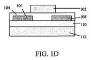
図1Aにおいて、有機電界効果トランジスタ(OTFT)は概略的に説明され、「底面接触モード」におけるそのようなデバイスの電気活性層の相対的な位置を示す。(OTFTの「底面接触モード」において、ソースおよびドレイン電極ならびに任意の残存する曝露されたゲート誘電層上へ電気活性有機半導体層を堆積させる前に、ドレインおよびソース電極はゲート誘電層上へ堆積される。)基板112は、ゲート電極102および絶縁層104と接触しており、その上にソース電極106およびドレイン電極108が堆積される。ソースおよびドレイン電極の上部および間は、式Iまたは式IIのピリミジン化合物を含んでなる有機半導体層110である。 In FIG. 1A, an organic field effect transistor (OTFT) is schematically illustrated and shows the relative position of the electroactive layer of such a device in “bottom contact mode”. (In “bottom contact mode” of OTFT, the drain and source electrodes are deposited on the gate dielectric layer before depositing the electroactive organic semiconductor layer on the source and drain electrodes and any remaining exposed gate dielectric layer. The
図1Bは、上面接触モードにおけるそのようなデバイスの電気活性層の相対的な位置を示すOTFTの概略図である。(「上面接触モード」において、OTFTのドレインおよびソース電極は電気活性有機半導体層上面へ堆積される。) FIG. 1B is a schematic diagram of an OTFT showing the relative position of the electroactive layer of such a device in top contact mode. (In “top contact mode”, the drain and source electrodes of the OTFT are deposited on top of the electroactive organic semiconductor layer.)
図1Cは、ゲートが上面にある底面接触モードのそのようなデバイスの電気活性層の相対的な位置を示すOTFTの概略図である。 FIG. 1C is a schematic diagram of an OTFT showing the relative position of the electroactive layer of such a device in bottom contact mode with the gate on top.
図1Dは、ゲートが上面にある上面接触モードのそのようなデバイスの電気活性層の相対的な位置を示すOTFTの概略図である。 FIG. 1D is a schematic diagram of an OTFT showing the relative position of the electroactive layer of such a device in top contact mode with the gate on top.
基板は、無機ガラス、セラミック箔、ポリマー材料(例えば、アクリル、エポキシ、ポリアミド、ポリカーボネート、ポリイミド、ポリケトン、ポリ(オキシ−1,4−フェニレンオキシ−1,4−フェニレンカルボニル−1,4−フェニレン)(ポリ(エーテルエーテルケトン)またはPEEKと呼ばれることもある)、ポリノルボルネン、ポリフェニレンオキシド、ポリ(エチレンナフタレンジカルボキシレート)(PEN)、ポリ(エチレンテレフタレート)(PET)、ポリ(フェニレンスルフィド)(PPS))、充填ポリマー材料(例えば、繊維強化プラスチック(FRP))、および/またはコーティングされた金属箔を含んでなることが可能である。基板の厚さは、約10マイクロメートル〜10ミリメートル超であることが可能であり、例えば、可撓性プラスチック基板に関しては約50〜約100マイクロメートル、そしてガラスまたはシリコンなどの剛性基板に関しては約1〜約10ミリメートルであることが可能である。典型的に、基板は、製造、試験および/または使用の間、OTFTを支持する。任意選択で、基板は、ソース、ドレインおよび電極へのバスライン接続、ならびにOTFTのための回路などの電気的機能を提供することができる。 The substrate is inorganic glass, ceramic foil, polymer material (for example, acrylic, epoxy, polyamide, polycarbonate, polyimide, polyketone, poly (oxy-1,4-phenyleneoxy-1,4-phenylenecarbonyl-1,4-phenylene) (Sometimes called poly (ether ether ketone) or PEEK), polynorbornene, polyphenylene oxide, poly (ethylene naphthalene dicarboxylate) (PEN), poly (ethylene terephthalate) (PET), poly (phenylene sulfide) (PPS) )), Filled polymeric material (eg, fiber reinforced plastic (FRP)), and / or coated metal foil. The thickness of the substrate can be greater than about 10 micrometers to 10 millimeters, for example, about 50 to about 100 micrometers for flexible plastic substrates, and about about rigid substrates such as glass or silicon. It can be from 1 to about 10 millimeters. Typically, the substrate supports the OTFT during manufacturing, testing and / or use. Optionally, the substrate can provide electrical functions such as bus line connections to sources, drains and electrodes, and circuitry for OTFTs.
ゲート電極は、金属薄膜、導電性ポリマー膜、導電性インクもしくはペーストから製造された導電性膜、または基板自体、例えば高濃度にドープされたシリコンであることができる。適切なゲート電極材料の例には、アルミニウム、金、クロム、インジウムスズ酸化物、ポリスチレンスルホネートがドープされたポリ(3,4−エチレンジオキシチオフェン)(PSS−PEDOT)などの導電性ポリマー、カーボンブラック/グラファイトから構成される導電性インク/ペースト、または高分子バインダー中のコロイド状銀の分散系が含まれる。いくつかのOTFTにおいては、同一材料でゲート電極機能を提供することができ、また基板の支持体機能を提供することができる。例えば、ドープされたシリコンはゲート電極として機能することができ、OTFTを支持することができる。 The gate electrode can be a metal thin film, a conductive polymer film, a conductive film made from a conductive ink or paste, or the substrate itself, eg, highly doped silicon. Examples of suitable gate electrode materials include conductive polymers such as aluminum, gold, chromium, indium tin oxide, poly (3,4-ethylenedioxythiophene) doped with polystyrene sulfonate (PSS-PEDOT), carbon A conductive ink / paste composed of black / graphite or a colloidal silver dispersion in a polymeric binder is included. In some OTFTs, the same material can provide a gate electrode function and can also provide a substrate support function. For example, doped silicon can function as a gate electrode and can support an OTFT.
ゲート電極を、真空蒸発、金属または導電性金属酸化物のスパッタリング、スピンコーティング、キャスティング、または印刷による導電性ポリマー溶液または導電性インクのコーティングによって調製することができる。ゲート電極の厚さは、例えば、金属膜に関しては約10〜約200ナノメートル、そしてポリマー導体に関しては約1〜約10マイクロメートルであることが可能である。 The gate electrode can be prepared by coating a conductive polymer solution or conductive ink by vacuum evaporation, sputtering of a metal or conductive metal oxide, spin coating, casting, or printing. The thickness of the gate electrode can be, for example, from about 10 to about 200 nanometers for metal films and from about 1 to about 10 micrometers for polymer conductors.
ソースおよびドレイン電極は、半導体層とソースおよびドレイン電極との間の接触の抵抗が半導体層の抵抗より低いように、低い抵抗接点を半導体層にもたらす材料から製造することができる。チャネル抵抗は、半導体層の伝導性である。典型的に、抵抗はチャネル抵抗未満である。ソースおよびドレイン電極としての使用に適切な典型的な材料には、アルミニウム、バリウム、カルシウム、クロム、金、銀、ニッケル、パラジウム、白金、チタンおよびそれらの合金、カーボンナノチューブ、ポリアニリンおよびポリ(3,4−エチレンジオキシチオフェン)/ポリ−(スチレンスルホネート)(PEDOT:PSS)などの導電性ポリマー、導電性ポリマー中のカーボンナノチューブの分散系、導電性ポリマー中の金属の分散系、ならびにそれらの多層フィルムが含まれる。当業者に既知であるように、これらの材料のいくつかはN型半導体材料の用途に適切であり、そして他はP型半導体材料の用途に適切である。ソースおよびドレイン電極の典型的な厚さはおおよそ、例えば、約40ナノメートル〜約1マイクロメートルである。いくつかの実施形態において、厚さは約100〜約400ナノメートルである。 The source and drain electrodes can be made from a material that provides a low resistance contact to the semiconductor layer such that the resistance of the contact between the semiconductor layer and the source and drain electrodes is lower than the resistance of the semiconductor layer. Channel resistance is the conductivity of the semiconductor layer. Typically, the resistance is less than the channel resistance. Typical materials suitable for use as source and drain electrodes include aluminum, barium, calcium, chromium, gold, silver, nickel, palladium, platinum, titanium and their alloys, carbon nanotubes, polyaniline and poly (3, Conductive polymers such as 4-ethylenedioxythiophene) / poly- (styrene sulfonate) (PEDOT: PSS), dispersions of carbon nanotubes in conductive polymers, dispersions of metals in conductive polymers, and multilayers thereof Film is included. As is known to those skilled in the art, some of these materials are suitable for N-type semiconductor material applications, and others are suitable for P-type semiconductor material applications. Typical thicknesses of the source and drain electrodes are approximately, for example, from about 40 nanometers to about 1 micrometer. In some embodiments, the thickness is from about 100 to about 400 nanometers.
絶縁層は、無機材料膜または有機ポリマー膜を含んでなる。絶縁層として適切な無機材料の実例としては、酸化アルミニウム、酸化ケイ素、酸化タンタル、酸化チタン、窒化ケイ素、チタン酸バリウム、チタン酸バリウムストロンチウム、チタン酸ジルコン酸バリウム、セレン化亜鉛および硫化亜鉛が含まれる。加えて、上記材料の合金、組み合わせおよび多層フィルムを絶縁層に使用することができる。絶縁層のための有機ポリマーの実例としては、ポリエステル、ポリカーボネート、ポリ(ビニルフェノール)、ポリイミド、ポリスチレン、ポリ(メタクリレート)、ポリ(アクリレート)、エポキシ樹脂、ならびにそれらのブレンドおよび多層フィルムが含まれる。絶縁層の厚さは、使用される誘電体材料の誘電率に応じて、例えば約10ナノメートル〜約500ナノメートルである。例えば、絶縁層の厚さは約100ナノメートル〜約500ナノメートルであることができる。絶縁層は、例えば、約10−12S/cm(S=ジーメンス=1/オーム)未満である伝導性を有することができる。The insulating layer includes an inorganic material film or an organic polymer film. Examples of suitable inorganic materials for the insulating layer include aluminum oxide, silicon oxide, tantalum oxide, titanium oxide, silicon nitride, barium titanate, barium strontium titanate, barium zirconate titanate, zinc selenide and zinc sulfide. It is. In addition, alloys, combinations and multilayer films of the above materials can be used for the insulating layer. Illustrative organic polymers for the insulating layer include polyester, polycarbonate, poly (vinylphenol), polyimide, polystyrene, poly (methacrylate), poly (acrylate), epoxy resins, and blends and multilayer films thereof. The thickness of the insulating layer is, for example, from about 10 nanometers to about 500 nanometers, depending on the dielectric constant of the dielectric material used. For example, the thickness of the insulating layer can be from about 100 nanometers to about 500 nanometers. The insulating layer can have a conductivity that is, for example, less than about 10−12 S / cm (S = Siemens = 1 / Ohm).
絶縁層、ゲート電極、半導体層、ソース電極およびドレイン電極は、ゲート電極および半導体層の両方が絶縁層と接触し、そしてソース電極およびドレイン電極の両方が半導体層と接触する限り、任意の配列で形成される。「任意の配列で」という句は、連続および同時形成を含む。例えば、ソース電極およびドレイン電極は、同時に、または連続的に形成されることができる。ゲート電極、ソース電極およびドレイン電極は、物理気相堆積(例えば、熱蒸発またはスパッタリング)、あるいはインクジェット印刷などの既知の方法を使用して提供されることができる。電極のパターン化は、シャドーマスキング、アディティブフォトリソグラフィー、サブトラクティブフォトリソグラフィー、印刷、マイクロコンタクト印刷およびパターンコーティングなどの既知の方法によって達成することができる。 The insulating layer, gate electrode, semiconductor layer, source electrode and drain electrode can be in any arrangement as long as both the gate electrode and semiconductor layer are in contact with the insulating layer and both the source electrode and drain electrode are in contact with the semiconductor layer. It is formed. The phrase “in any sequence” includes sequential and simultaneous formation. For example, the source electrode and the drain electrode can be formed simultaneously or sequentially. The gate electrode, source electrode and drain electrode can be provided using known methods such as physical vapor deposition (eg, thermal evaporation or sputtering) or ink jet printing. Electrode patterning can be accomplished by known methods such as shadow masking, additive photolithography, subtractive photolithography, printing, microcontact printing and pattern coating.
底面接触モードのOTFに関して(図1A)、フォトリソグラフ法を使用して、それぞれソースおよびドレインのためのチャネルを形成する電極106および108を二酸化ケイ素層上に形成することができる。次いで、半導体層110を、電極106および108ならびに層104の表面上に堆積する。 For bottom contact mode OTF (FIG. 1A), photolithography can be used to form
一実施形態において、半導体層110は式Iまたは式IIによって表される1種またはそれ以上の化合物を含んでなる。半導体層110は、当該技術で既知の様々な技術によって堆積することができる。これらの技術には、熱蒸発、化学気相堆積、熱移動、インクジェット印刷およびスクリーン印刷が含まれる。堆積のための分散系薄膜コーティング技術には、スピンコーティング、ドクターブレードコーティング、ドロップキャスティングおよび他の既知の技術が含まれる。 In one embodiment, the
上面接触モードのOTFTに関して(図1B)、電極106および108の製造の前に、層110を層104上に堆積する。 For top contact mode OTFT (FIG. 1B),
b.第2の例示的なデバイス
また本発明は、2層の電気接触層の間に配置される少なくとも1層の電気活性層を含んでなり、デバイスの少なくとも1層の電気活性層が、式Iまたは式IIを有するピリミジン化合物を含む電子デバイスに関する。b. Second Exemplary Device The present invention also comprises at least one electroactive layer disposed between two electrical contact layers, wherein at least one electroactive layer of the device is of formula I or It relates to an electronic device comprising a pyrimidine compound having the formula II.
有機電子デバイス構造の別の例を図2に示す。デバイス200は、第1の電気接触層、アノード層210、第2の電気接触層、カソード層260、およびそれらの間の光活性層240を有する。アノードに隣接して、正孔注入層220が存在してもよい。正孔注入層に隣接して、正孔輸送材料を含んでなる正孔輸送層230が存在してもよい。カソードに隣接して、電子輸送材料を含んでなる電子輸送層250が存在してもよい。デバイスは、アノード210の隣に1つ以上の追加の正孔注入層または正孔輸送層(図示せず)、および/またはカソード260の隣に1つ以上の追加の電子注入または電子輸送層(図示せず)を使用することができる。 Another example of an organic electronic device structure is shown in FIG. The
層220〜250は、個々に、そして集合的に、電気活性層と呼ばれる。 Layers 220-250 are referred to individually and collectively as electroactive layers.
いくつかの実施形態において、光活性層240は図3で示すようにピクセル化される。層240は層上に繰り返されるピクセルまたはサブピクセルユニット241、242および243に分離される。各ピクセルまたはサブピクセルユニットは異なる色を表す。いくつかの実施形態において、サブピクセルユニットは、赤色、緑色、青色である。3つのサブピクセルユニットが図に示されるが、2つまたは4つ以上が使用されてもよい。 In some embodiments, the
一実施形態において、種々の層は以下の厚さの範囲を有する。アノード210、500〜5000Å、一実施形態において1000〜2000Å、正孔注入層220、50〜2000Å、一実施形態において200〜1000Å、正孔輸送層230、50〜2000Å、一実施形態において200〜1000Å、電気活性層240、10〜2000Å、一実施形態において100〜1000Å、層250、50〜2000Å、一実施形態において100〜1000Å、カソード260、200〜10000Å、一実施形態において300〜5000Å。デバイスの電子正孔再結合領域の位置、したがって、デバイスの発光スペクトルは、各層の相対的な厚さに影響を受けることができる。層の厚さの所望の比は、使用される材料の厳密な性質に依存する。いくつかの実施形態において、デバイスは、処理を補助するか、機能性を改善するための追加的な層を有する。 In one embodiment, the various layers have the following thickness ranges:
デバイス200の用途によって、光活性層240は、印加電圧によって活性化される発光層(発光ダイオードまたは発光電気化学電池など)、あるいは印加バイアス電圧の有無にかかわらず放射エネルギーに反応して信号を生じる材料の層(光検出器など)であることができる。光検出器の例には、光伝導電池、フォトレジスタ、フォトスイッチ、フォトトランジスタおよび光電管、ならびに光電池が含まれる。これらの用語については、Markus,John,Electronics and Nucleonics Dictionary,470 and 476(McGraw−Hill,Inc.1966)に説明されているとおりである。発光層を有するデバイスは、ディスプレイを形成するため、または白色光証明器具などの照明用途のために使用されてもよい。 Depending on the application of the
本明細書に記載される新規電気活性化合物の1種またはそれ以上が、デバイスの電気活性層の1層またはそれ以上に存在しもよい。 One or more of the novel electroactive compounds described herein may be present in one or more of the electroactive layers of the device.
いくつかの実施形態において、式Iまたは式IIを有する新規電気活性化合物は、光活性層240の光活性ドーパント材料のためのホスト材料として有用である。これらの化合物が単独で、または他の共ホストとともに使用される場合、OLEDデバイスの改善された効率および寿命がもたらされることが見出された。計算により、これらの化合物が、高いトリプレットエネルギー、ならびに電荷輸送に適切なHOMOおよびLUMO準位を有し、有機金属発光体のための優れたホスト材料となることが発見された。 In some embodiments, the novel electroactive compounds having Formula I or Formula II are useful as host materials for the photoactive dopant material of the
いくつかの実施形態において、新規電気活性化合物は、層250の電子輸送材料として有用である。 In some embodiments, the novel electroactive compound is useful as an electron transport material for
光活性層
いくつかの実施形態において、光活性層240は、上記電気活性組成物を含んでなる。Photoactive Layer In some embodiments, the
いくつかの実施形態において、ドーパントは有機金属材料である。いくつかの実施形態において、有機金属材料は、IrまたはPtの錯体である。いくつかの実施形態において、有機金属材料は、Irのシクロメタレート化された錯体である。 In some embodiments, the dopant is an organometallic material. In some embodiments, the organometallic material is a complex of Ir or Pt. In some embodiments, the organometallic material is a cyclometallated complex of Ir.
いくつかの実施形態において、光活性層は、(a)式Iまたは式IIを有するピリミジン化合物であるホスト材料、および(b)1種またはそれ以上のドーパントを含んでなる。いくつかの実施形態において、光活性層は、(a)式Iまたは式IIを有するピリミジン化合物であるホスト材料、および(b)有機金属エレクトロルミネセントドーパントを含んでなる。いくつかの実施形態において、光活性層は、(a)式Iまたは式IIを有するピリミジン化合物であるホスト材料、(b)光活性ドーパント、および(c)第2のホスト材料を含んでなる。いくつかの実施形態において、光活性層は、(a)式Iまたは式IIを有するピリミジン化合物であるホスト材料、(b)IrまたはPtの有機金属錯体、および(c)第2のホスト材料を含んでなる。いくつかの実施形態において、光活性層は、(a)式Iまたは式IIを有するピリミジン化合物であるホスト材料、(b)Irのシクロメタレート化錯体、および(c)第2のホスト材料を含んでなる。 In some embodiments, the photoactive layer comprises (a) a host material that is a pyrimidine compound having Formula I or Formula II, and (b) one or more dopants. In some embodiments, the photoactive layer comprises (a) a host material that is a pyrimidine compound having Formula I or Formula II, and (b) an organometallic electroluminescent dopant. In some embodiments, the photoactive layer comprises (a) a host material that is a pyrimidine compound having Formula I or Formula II, (b) a photoactive dopant, and (c) a second host material. In some embodiments, the photoactive layer comprises (a) a host material that is a pyrimidine compound having Formula I or Formula II, (b) an organometallic complex of Ir or Pt, and (c) a second host material. Comprising. In some embodiments, the photoactive layer comprises (a) a host material that is a pyrimidine compound having Formula I or Formula II, (b) a cyclometallated complex of Ir, and (c) a second host material. Comprising.
いくつかの実施形態において、光活性層は、(a)式Iまたは式IIを有するピリミジン化合物であるホスト材料、および(b)1種またはそれ以上のドーパントから本質的になる。いくつかの実施形態において、光活性層は、(a)式Iまたは式IIを有する化合物であるホスト材料、および(b)有機金属エレクトロルミネセントドーパントから本質的になる。いくつかの実施形態において、光活性層は、(a)式Iまたは式IIを有するピリミジン化合物であるホスト材料、(b)光活性ドーパント、および(c)第2のホスト材料から本質的になる。いくつかの実施形態において、光活性層は、(a)式Iまたは式IIを有するピリミジン化合物であるホスト材料、(b)IrまたはPtの有機金属錯体、および(c)第2のホスト材料から本質的になる。いくつかの実施形態において、光活性層は、(a)式Iまたは式IIを有するピリミジン化合物であるホスト材料、(b)Irのシクロメタレート化錯体、および(c)第2のホスト材料から本質的になる。 In some embodiments, the photoactive layer consists essentially of (a) a host material that is a pyrimidine compound having Formula I or Formula II, and (b) one or more dopants. In some embodiments, the photoactive layer consists essentially of (a) a host material that is a compound having Formula I or Formula II, and (b) an organometallic electroluminescent dopant. In some embodiments, the photoactive layer consists essentially of (a) a host material that is a pyrimidine compound having Formula I or Formula II, (b) a photoactive dopant, and (c) a second host material. . In some embodiments, the photoactive layer comprises (a) a host material that is a pyrimidine compound having Formula I or Formula II, (b) an organometallic complex of Ir or Pt, and (c) a second host material. Become essential. In some embodiments, the photoactive layer comprises (a) a host material that is a pyrimidine compound having Formula I or Formula II, (b) a cyclometallated complex of Ir, and (c) a second host material. Become essential.
いくつかの実施形態において、光活性層は、(a)化合物が重水素化された式Iまたは式IIを有するピリミジン化合物であるホスト材料、および(b)1種またはそれ以上のドーパントから本質的になる。いくつかの実施形態において、光活性層は、(a)化合物が重水素化された式Iまたは式IIを有するピリミジン化合物であるホスト材料、および(b)有機金属エレクトロルミネセントドーパントから本質的になる。いくつかの実施形態において、光活性層は、(a)化合物が重水素化された式Iまたは式IIを有するピリミジン化合物であるホスト材料、(b)光活性ドーパント、および(c)第2のホスト材料から本質的になる。いくつかの実施形態において、光活性層は、(a)化合物が重水素化された式Iまたは式IIを有するピリミジン化合物であるホスト材料、化合物が重水素化された式Iまたは式IIを有するピリミジン化合物であるホスト材料、(b)IrまたはPtの有機金属錯体、および(c)第2のホスト材料から本質的になる。いくつかの実施形態において、光活性層は、(a)化合物が重水素化された式Iまたは式IIを有するピリミジン化合物であるホスト材料、(b)Irのシクロメタレート化錯体、および(c)第2のホスト材料から本質的になる。いくつかの実施形態において、式Iまたは式IIの重水素化された化合物は少なくとも10%重水素化され、いくつかの実施形態において、少なくとも50%重水素化される。いくつかの実施形態において、第2のホスト材料は重水素化される。いくつかの実施形態において、第2のホスト材料は少なくとも10%重水素化され、いくつかの実施形態において、少なくとも50%重水素化される。 In some embodiments, the photoactive layer consists essentially of (a) a host material wherein the compound is a deuterated pyrimidine compound having Formula I or Formula II, and (b) one or more dopants. become. In some embodiments, the photoactive layer consists essentially of (a) a host material wherein the compound is a deuterated pyrimidine compound having Formula I or Formula II, and (b) an organometallic electroluminescent dopant. Become. In some embodiments, the photoactive layer comprises (a) a host material, wherein the compound is a deuterated pyrimidine compound having Formula I or Formula II, (b) a photoactive dopant, and (c) a second It consists essentially of a host material. In some embodiments, the photoactive layer has (a) a host material in which the compound is a deuterated pyrimidine compound having Formula I or Formula II, a compound in which the compound is deuterated, Formula I or Formula II It consists essentially of a host material that is a pyrimidine compound, (b) an organometallic complex of Ir or Pt, and (c) a second host material. In some embodiments, the photoactive layer comprises (a) a host material wherein the compound is a deuterated pyrimidine compound having Formula I or Formula II, (b) a cyclometallated complex of Ir, and (c ) Consisting essentially of a second host material. In some embodiments, the deuterated compound of Formula I or Formula II is at least 10% deuterated, and in some embodiments, at least 50% deuterated. In some embodiments, the second host material is deuterated. In some embodiments, the second host material is at least 10% deuterated, and in some embodiments, at least 50% deuterated.
電子輸送層
式IおよびIIのピリミジン化合物は、層250の電子輸送材料として有用である。化合物は単独でも、別の電子輸送材料と組み合わせても使用することができる。いくつかの実施形態において、電子輸送層は、式IまたはIIのピリミジン化合物から本質的になる。Electron Transport Layer Pyrimidine compounds of formulas I and II are useful as the electron transport material for
単独で、またはピリミジン化合物と組み合わせて使用することができる他の電子輸送材料の例としては、限定されないが、トリス(8−ヒドロキシキノラト)アルミニウム(AlQ)、ビス(2−メチル−8−キノリノラト)(p−フェニルフェノラト)アルミニウム(BAlq)、テトラキス−(8−ヒドロキシキノラト)ハフニウム(HfQ)、およびテトラキス−(8−ヒドロキシキノラト)ジルコニウム(ZrQ)などの金属キノレート誘導体などを含む金属キレート化オキシノイド化合物;ならびに2−(4−ビフェニリル)−5−(4−t−ブチルフェニル)−1,3,4−オキサジアゾール(PBD)、3−(4−ビフェニリル)−4−フェニル−5−(4−t−ブチルフェニル)−1,2,4−トリアゾール(TAZ)、および1,3,5−トリ(フェニル−2−ベンズイミダゾール)ベンゼン(TPBI)などのアゾール化合物;2,3−ビス(4−フルオロフェニル)キノキサリンなどのキノキサリン誘導体;4,7−ジフェニル−1,10−フェナントロリン(DPA)および2,9−ジメチル−4,7−ジフェニル−1,10−フェナントロリン(DDPA)などのフェナントロリン;ならびにそれらの混合物が挙げられる。いくつかの実施形態において、電子輸送材料は、金属キノレートおよびフェナントロリン誘導体からなる群から選択される。いくつかの実施形態において、電子輸送層は、n−ドーパントをさらに含む。n−ドーパント材料は周知である。n−ドーパントとしては、限定されないが、1族および2族金属;1族および2族金属の塩、例えば、LiF、CsF、およびCs2CO3;1族および2族金属の有機化合物、例えばLiキノレート;ならびに分子n−ドーパント、例えばロイコ染料、W2(hpp)4(式中、hpp=1,3,4,6,7,8−ヘキサヒドロ−2H−ピリミド−[1,2−a]−ピリミジンである)などの金属錯体、ならびにコバルトセン、テトラチアナフタセン、ビス(エチレンジチオ)テトラチアフルバレン、複素環式ラジカルまたはジラジカル、ならびに複素環式ラジカルまたはジラジカルのダイマー、オリゴマー、ポリマー、ジスピロ化合物、および多環化合物が挙げられる。Examples of other electron transport materials that can be used alone or in combination with pyrimidine compounds include, but are not limited to, tris (8-hydroxyquinolato) aluminum (AlQ), bis (2-methyl-8-quinolinolato). Metals including metal quinolate derivatives such as (p-phenylphenolato) aluminum (BAlq), tetrakis- (8-hydroxyquinolato) hafnium (HfQ), and tetrakis- (8-hydroxyquinolato) zirconium (ZrQ) Chelated oxinoid compounds; and 2- (4-biphenylyl) -5- (4-tert-butylphenyl) -1,3,4-oxadiazole (PBD), 3- (4-biphenylyl) -4-phenyl- 5- (4-t-butylphenyl) -1,2,4-triazole (TAZ), Azole compounds such as 1,3,5-tri (phenyl-2-benzimidazole) benzene (TPBI); quinoxaline derivatives such as 2,3-bis (4-fluorophenyl) quinoxaline; 4,7-diphenyl-1, Phenanthrolines such as 10-phenanthroline (DPA) and 2,9-dimethyl-4,7-diphenyl-1,10-phenanthroline (DDPA); and mixtures thereof. In some embodiments, the electron transport material is selected from the group consisting of metal quinolates and phenanthroline derivatives. In some embodiments, the electron transport layer further comprises an n-dopant. n-dopant materials are well known. n-dopants include, but are not limited to, Group 1 and Group 2 metals; Group 1 and Group 2 metal salts, such as LiF, CsF, and Cs2 CO3 ; Group 1 and Group 2 metal organic compounds, such as Li Quinolate; and molecular n-dopants such as leuco dyes, W2 (hpp)4 , where hpp = 1,3,4,6,7,8-hexahydro-2H-pyrimido- [1,2-a]- Metal complexes such as pyrimidine), and cobalt cene, tetrathianaphthacene, bis (ethylenedithio) tetrathiafulvalene, heterocyclic radicals or diradicals, and heterocyclic radicals or diradical dimers, oligomers, polymers, dispiro compounds , And polycyclic compounds.
他のデバイス層
デバイスの他の層は、そのような層で有用であることが知られている任意の材料から製造することができる。Other Device Layers Other layers of the device can be made from any material known to be useful in such layers.
アノード210は、正電荷キャリアの注入に特に有効な電極である。これは、例えば、金属、混合金属、合金、金属酸化物、または混合金属酸化物を含有する材料から製造することができ、あるいは導電性ポリマー、またはそれらの混合物でることもできる。適切な金属としては、11族金属、4〜6族金属および8〜10族遷移金属が挙げられる。アノードが光透過性となる場合には、インジウムスズ酸化物などの12族、13族、および14族金属の混合金属酸化物が一般に使用される。アノード210は、“Flexible light−emitting diodes made from soluble conducting polymer”,Nature vol.357,pp477−479(1992年6月11日)に記載されるようなポリアニリンなどの有機材料を含んでなることができる。アノードおよびカソードの少なくとも1つは、発生した光を観察できるように、望ましくは少なくとも部分的に透明となる。 The
正孔注入層220は正孔注入材料を含んでなり、有機電子デバイスにおいて、限定されないが、下にある層の平坦化、電荷輸送および/または電荷注入特性、酸素または金属イオンなどの不純物の捕捉、ならびに有機電子デバイスの性能を促進または改善する他の特徴を含む1つ以上の機能を有することができる。正孔注入材料は、ポリマー、オリゴマーまたは小分子でもよい。それらは気相堆積されるか、あるいは溶液、分散系、懸濁液、エマルジョン、コロイド状混合物または他の組成物の形態であってもよい液体から堆積されてもよい。 The
正孔注入層は、プロトン酸がしばしばドープされるポリアニリン(PANI)またはポリエチレンジオキシチオフェン(PEDOT)などのポリマー材料を使用して形成することができる。プロトン酸は、例えば、ポリ(スチレンスルホン酸)、ポリ(2−アクリルアミド−2−メチル−1−プロパンスルホン酸)などであることができる。 The hole injection layer can be formed using a polymer material such as polyaniline (PANI) or polyethylenedioxythiophene (PEDOT), which is often doped with a protonic acid. The protic acid can be, for example, poly (styrenesulfonic acid), poly (2-acrylamido-2-methyl-1-propanesulfonic acid), and the like.
正孔注入層は、銅フタロシアニンおよびテトラチアフルバレン−テトラシアノキノジメタン系(TTF−TCNQ)などの電荷輸送化合物などを含むことができる。 The hole injection layer can include copper phthalocyanine and a charge transport compound such as tetrathiafulvalene-tetracyanoquinodimethane (TTF-TCNQ).
いくつかの実施形態において、正孔注入層は、少なくとも1種の導電性ポリマーと少なくとも1種のフッ素化酸ポリマーとを含んでなる。いくつかの実施形態において、正孔注入層は、フッ素化酸ポリマーでドープされた導電性ポリマーを含んでなる。材料は、例えば、米国特許出願公開第2004/0102577号明細書、同第2004/0127637号明細書、同第2005/0205860号明細書および国際公開第2009/018009号パンフレットに記載されている。 In some embodiments, the hole injection layer comprises at least one conductive polymer and at least one fluorinated acid polymer. In some embodiments, the hole injection layer comprises a conductive polymer doped with a fluorinated acid polymer. The materials are described in, for example, US Patent Application Publication Nos. 2004/0102577, 2004/0127637, 2005/0205860, and International Publication No. 2009/018009.
層230の正孔輸送材料の例は、例えば、Y.Wangにより,Kirk−Othmer Encyclopedia of Chemical Technology,Fourth Edition,Vol.18,p.837−860,1996にまとめられている。正孔輸送分子およびポリマーの両方を使用することができる。一般に使用される正孔輸送分子としては、N,N’−ジフェニル−N,N’−ビス(3−メチルフェニル)−[1,1’−ビフェニル]−4,4’−ジアミン(TPD)、1,1−ビス[(ジ−4−トリルアミノ)フェニル]シクロヘキサン(TAPC)、N,N’−ビス(4−メチルフェニル)−N,N’−ビス(4−エチルフェニル)−[1,1’−(3,3’−ジメチル)ビフェニル]−4,4’−ジアミン(ETPD)、テトラキス−(3−メチルフェニル)−N,N,N’,N’−2,5−フェニレンジアミン(PDA)、α−フェニル−4−N,N−ジフェニルアミノスチレン(TPS)、p−(ジエチルアミノ)ベンズアルデヒドジフェニルヒドラゾン(DEH)、トリフェニルアミン(TPA)、ビス[4−(N,N−ジエチルアミノ)−2−メチルフェニル](4−メチルフェニル)メタン(MPMP)、1−フェニル−3−[p−(ジエチルアミノ)スチリル]−5−[p−(ジエチルアミノ)フェニル]ピラゾリン(PPRまたはDEASP)、1,2−トランス−ビス(9H−カルバゾール−9−イル)シクロブタン(DCZB)、N,N,N’,N’−テトラキス(4−メチルフェニル)−(1,1’−ビフェニル)−4,4’−ジアミン(TTB)、N,N’−ビス(ナフタレン−1−イル)−N,N’−ビス−(フェニル)ベンジジン(α−NPB)、および銅フタロシアニンなどのポルフィリン系化合物が挙げられる。一般に使用される正孔輸送ポリマーは、ポリビニルカルバゾール、(フェニルメチル)ポリシラン、およびポリアニリンである。ポリスチレンおよびポリカーボネートなどのポリマー中に上記などの正孔輸送分子をドープすることによって、正孔輸送ポリマーを得ることもできる。場合によっては、トリアリールアミンポリマー、特にトリアリールアミン−フルオレンコポリマーが使用される。場合によっては、これらのポリマーおよびコポリマーは架橋性である。いくつかの実施形態において、正孔輸送層は、p−ドーパントをさらに含んでなる。いくつかの実施形態において、正孔輸送層は、p−ドーパントでドープされる。p−ドーパントの例には、限定されないが、テトラフルオロテトラシアノキノジメタン(F4−TCNQ)およびペリレン−3,4,9,10−テトラカルボン酸−3,4,9,10−二無水物(PTCDA)が含まれる。 Examples of hole transport materials for
カソード260は、電子または負電荷キャリアの注入に特に効率的な電極である。カソードは、アノードよりも低い仕事関数を有するいずれの金属または非金属であってよい。カソードの材料は、1族のアルカリ金属(例えば、Li、Cs)、2族(アルカリ土類)金属、12族金属、例えば希土類元素およびランタニド、ならびにアクチニドから選択することができる。アルミニウム、インジウム、カルシウム、バリウム、サマリウム、およびマグネシウム、ならびにそれらの組み合わせなどの材料を使用することができる。作動電圧を下げるために、Li−またはCs含有有機金属化合物、LiF、CsF、およびLi2Oを有機層とカソード層との間に堆積することもできる。The
有機電子デバイス中に別の層が存在することが知られている。例えば、注入される正電荷の量を制御するため、および/または層のバンドギャップを一致させるため、または保護層として機能させるために、アノード210と正孔注入層220との間に層(図示せず)が存在することができる。銅フタロシアニン、ケイ素オキシ窒化物、フルオロカーボン、シラン、またはPtなどの金属の超薄層などの当技術分野において周知の層を使用することができる。あるいは、アノード層210、電気活性層220、230、240および250、またはカソード層260の一部または全てを、電荷キャリア輸送効率を増加させるために表面処理することができる。それぞれの構成層の材料の選択は、好ましくは、高エレクトロルミネッセンス効率を有するデバイスを得るために発光層中の正電荷および負電荷のバランスがとられるように行われる。 It is known that another layer exists in organic electronic devices. For example, to control the amount of positive charge injected and / or to match the band gap of the layer or to function as a protective layer, a layer (see FIG. (Not shown) can exist. Layers well known in the art such as copper phthalocyanine, silicon oxynitride, fluorocarbon, silane, or ultrathin layers of metals such as Pt can be used. Alternatively, some or all of
それぞれの機能層を2層以上の層で構成することができることは理解される。 It is understood that each functional layer can be composed of two or more layers.
適切な基板上での個々の層の連続的気相堆積を含む様々な技術によって、デバイスを調製することができる。ガラス、プラスチックおよび金属などの基板を使用することができる。熱蒸発、化学気相堆積などの従来の気相堆積技術を使用することができる。あるいは、限定されないが、スピンコーティング、ディップコーティング、ロール−ツー−ロール技術、インクジェット印刷、スクリーン印刷、グラビア印刷などを含む従来のコーティングまたは印刷技術を使用して、適切な溶媒中の溶液または分散系から有機層を塗布することができる。 The device can be prepared by a variety of techniques including sequential vapor deposition of individual layers on a suitable substrate. Substrates such as glass, plastic and metal can be used. Conventional vapor deposition techniques such as thermal evaporation, chemical vapor deposition and the like can be used. Alternatively, solutions or dispersions in a suitable solvent using conventional coating or printing techniques including but not limited to spin coating, dip coating, roll-to-roll techniques, ink jet printing, screen printing, gravure printing, etc. An organic layer can be applied.
いくつかの実施形態において、デバイスは、緩衝層、正孔輸送層および光活性層の液相堆積によって、そしてアノード、電子輸送層、電子注入層およびカソードの気相堆積によって製造される。 In some embodiments, the device is fabricated by liquid deposition of a buffer layer, a hole transport layer, and a photoactive layer, and by vapor deposition of an anode, an electron transport layer, an electron injection layer, and a cathode.
効率の高いLEDを達成するため、正孔輸送材料のHOMO(最高被占分子軌道)は、望ましくはアノードの仕事関数と一致し、そして電子伝達材料のLUMO(最低空分子軌道)は、望ましくはカソードの仕事関数と一致する。材料の化学適合性および昇華温度も、電子および正孔輸送材料を選択する時に考慮すべきこととなり得る。 In order to achieve a highly efficient LED, the HOMO (highest occupied molecular orbital) of the hole transport material desirably matches the work function of the anode, and the LUMO (lowest unoccupied molecular orbital) of the electron transfer material desirably Consistent with the work function of the cathode. The chemical compatibility and sublimation temperature of the material can also be considered when selecting electron and hole transport materials.
本明細書に記載のピリミジン化合物によって製造されるデバイスの効率を、デバイスの他の層を最適化することによってさらに改善することができることは理解される。例えば、Ca、BaまたはLiFなどのより効率的なカソードを使用することができる。作動電圧の低下をもたらすか、または量子効率を増加させる成形基板および新規正孔輸送材料も適用可能である。様々な層のエネルギー準位を調整し、エレクトロルミネセンスを促進するために、追加の層を加えることもできる。 It is understood that the efficiency of devices made with the pyrimidine compounds described herein can be further improved by optimizing other layers of the device. For example, more efficient cathodes such as Ca, Ba or LiF can be used. Shaped substrates and new hole transport materials that result in lower operating voltages or increase quantum efficiency are also applicable. Additional layers can be added to adjust the energy levels of the various layers and promote electroluminescence.
いくつかの実施形態において、式Iまたは式IIを有するピリミジン化合物は、デバイスの光活性層に存在する。いくつかの実施形態において、式Iまたは式IIを有するピリミジン化合物は、デバイスの電子輸送層に存在する。いくつかの実施形態において、式Iまたは式IIを有するピリミジン化合物がデバイスの光活性層に存在し、かつ式Iまたは式IIを有するピリミジン化合物がデバイスの電子輸送層に存在し、ピリミジン化合物は同一であることも、異なることも可能である。 In some embodiments, the pyrimidine compound having Formula I or Formula II is present in the photoactive layer of the device. In some embodiments, the pyrimidine compound having Formula I or Formula II is present in the electron transport layer of the device. In some embodiments, a pyrimidine compound having Formula I or Formula II is present in the photoactive layer of the device, and a pyrimidine compound having Formula I or Formula II is present in the electron transport layer of the device, and the pyrimidine compound is the same Can be different or different.
排他的ではない限り、上記デバイスの実施形態の任意の組み合わせであることが可能である。 Unless exclusive, it can be any combination of the above device embodiments.
本明細書に記載の概念を以下の実施例においてさらに説明するが、これらの実施例は、特許請求の範囲に記載される本発明の範囲を限定するものではない。 The concepts described herein are further illustrated in the following examples, which do not limit the scope of the invention described in the claims.
合成実施例1
本実施例は、化合物1、5−[3−(4,6−ビス−(3−ビフェニル)−2−ピリミジニル)フェニル]ピリミジンの合成を説明する。Synthesis Example 1
This example illustrates the synthesis of compound 1, 5- [3- (4,6-bis- (3-biphenyl) -2-pyrimidinyl) phenyl] pyrimidine.
(1a)5−(3−ブロモフェニル)ピリミジン(1a) 5- (3-Bromophenyl) pyrimidine
冷却器、温度計およびサイドアームストッパーを備えた1000mLの3つ口丸底フラスコに、1,2−ジメトキシエタン(315mL)中の3−ブロモヨードベンゼン(19.80g、70.0mmol)、ピリミジン−5−ボロン酸(8.67g、70.0mmol)の懸濁液および脱イオン水(105mL)中の炭酸ナトリウム(22.26g、210.0mmol)を添加した。混合物を30分間窒素スパージし、次いで、酢酸パラジウム(393mg、1.75mmol)およびトリフェニルホスフィン(918mg、3.50mmol)を添加した。反応混合物を還流下で18時間加熱し、次いで、UPLCによって完了したことが判定された後、室温まで冷却した。二相反応混合物をEtOAc(3×150mL)で抽出した。組み合わせた有機層を水およびブライン(各2×150mL)で洗浄し、次いで、MgSO4上で乾燥し、濾過および濃縮して、オフホワイト色固体を得た。これを、MPLC(ヘキサン/CHCl3)、それに続いて、無水エタノール(約200mL)からの結晶化によって精製し、所望の生成物である5−(3−ブロモフェニル)ピリミジンを得た(8.62g、収率63%)。この物質のUPLC分析によって、97.8%の純度を有することが示された。A 1000 mL 3-neck round bottom flask equipped with a condenser, thermometer and side arm stopper was charged with 3-bromoiodobenzene (19.80 g, 70.0 mmol), pyrimidine-in 1,2-dimethoxyethane (315 mL). A suspension of 5-boronic acid (8.67 g, 70.0 mmol) and sodium carbonate (22.26 g, 210.0 mmol) in deionized water (105 mL) were added. The mixture was sparged with nitrogen for 30 minutes, then palladium acetate (393 mg, 1.75 mmol) and triphenylphosphine (918 mg, 3.50 mmol) were added. The reaction mixture was heated under reflux for 18 hours and then cooled to room temperature after judged complete by UPLC. The biphasic reaction mixture was extracted with EtOAc (3 × 150 mL). The combined organic layers were washed with water and brine (2 × 150 mL each), then dried over MgSO4 , filtered and concentrated to give an off-white solid. This was purified by MPLC (hexane / CHCl3 ) followed by crystallization from absolute ethanol (ca. 200 mL) to give the desired product, 5- (3-bromophenyl) pyrimidine (8. 62 g, 63% yield). UPLC analysis of this material showed 97.8% purity.
(1b)5−[3−(4,4,5,5−テトラメチル−1,3,2−ジオキサボロラン−2−イル)フェニル]ピリミジン(1b) 5- [3- (4,4,5,5-tetramethyl-1,3,2-dioxaborolan-2-yl) phenyl] pyrimidine
磁気撹拌棒、内部温度計、およびサイドアームから使い捨てピペットを通して導入される窒素ラインを備えた250mLの3つ口丸底フラスコ中、乾燥1,4−ジオキサン(70mL)中の工程(1a)からの5−(3−ブロモフェニル)ピリミジン(3.30g、14.04mmol)およびビス(ピナコラト)ジボロン(4.28g、16.25mmol)の溶液に、酢酸カリウム(4.13g、42.1mmol)を添加した。攪拌している懸濁液に15分間窒素スパージした。[1,1−ビス(ジフェニルホスフィノ)フェロセン]パラジウム(II)クロリドジクロロメタン錯体(1:1)(344mg、0.42mmol)をさらなる1,4−ジオキサン(10mL)と一緒に添加し、そして窒素スパージをさらに10分間続けた。次いで、フラスコに、窒素バブラーを上部に取り付けた還流冷却器を取り付け、そして残りのサイドアームに栓をした。反応混合物を3.5時間還流下で加熱した。この時点でのUPLCによるアリコートの分析によると、生成物への完全な変換が示された。粗製反応混合物をシリカゲルのパッド(43g)に注入し、これをトルエン(2×100mL)ですすいだ。組み合わせた濾液を濃縮したところ、暗褐色油状物(5.0g)が得られた。50%EtOAc/ヘキサン(2×100mL)によるシリカゲルパッドのさらなる溶離によって、溶離液の濃縮後、UPLC分析によるとトルエン溶離からの茶色油状物と同一組成物を有する黄色油状物(1.2g)が得られた。2つの粗製生成物をジクロロメタン(合計100mL)に溶解し、組み合わせ、MPLC(EtOAc/ヘキサン)によって精製し、所望の生成物である5−[3−(4,4,5,5−テトラメチル−1,3,2−ジオキサボロラン−2−イル)フェニル]ピリミジン(3.56g、収率90%)を、静置時に凝固する淡黄色油状物として得た。 From step (1a) in dry 1,4-dioxane (70 mL) in a 250 mL three-necked round bottom flask equipped with a magnetic stir bar, internal thermometer, and nitrogen line introduced through a disposable pipette from the side arm. To a solution of 5- (3-bromophenyl) pyrimidine (3.30 g, 14.04 mmol) and bis (pinacolato) diboron (4.28 g, 16.25 mmol) was added potassium acetate (4.13 g, 42.1 mmol). did. The stirred suspension was sparged with nitrogen for 15 minutes. [1,1-bis (diphenylphosphino) ferrocene] palladium (II) chloride dichloromethane complex (1: 1) (344 mg, 0.42 mmol) was added along with additional 1,4-dioxane (10 mL) and nitrogen The sparging was continued for another 10 minutes. The flask was then fitted with a reflux condenser fitted with a nitrogen bubbler on top, and the remaining side arm was capped. The reaction mixture was heated under reflux for 3.5 hours. Analysis of an aliquot by UPLC at this point indicated complete conversion to product. The crude reaction mixture was poured into a pad of silica gel (43 g), which was rinsed with toluene (2 × 100 mL). The combined filtrate was concentrated to give a dark brown oil (5.0 g). Further elution of the silica gel pad with 50% EtOAc / hexane (2 × 100 mL) gave a yellow oil (1.2 g) with the same composition as the brown oil from toluene elution according to UPLC analysis after concentration of the eluent. Obtained. The two crude products were dissolved in dichloromethane (100 mL total), combined, purified by MPLC (EtOAc / hexanes) and the desired product 5- [3- (4,4,5,5-tetramethyl- 1,3,2-dioxaborolan-2-yl) phenyl] pyrimidine (3.56 g, 90% yield) was obtained as a pale yellow oil that solidified upon standing.
(1c)2−クロロ−4,6−ビス([1,1’−ビフェニル]−3−イル)ピリミジン(1c) 2-Chloro-4,6-bis ([1,1'-biphenyl] -3-yl) pyrimidine
磁気撹拌棒、温度計、還流冷却器および窒素バブラーを備えた1000mLの3つ口丸底フラスコに、脱イオン水(105mL)中、2,4,6−トリクロロピリミジン(9.17g、50.0mmol)、3−ビフェニルボロン酸(21.78g、110.0mmol)、トリフェニルホスフィン(656mg、2.50mmol)、1,2−ジメトキシエタン(375mL)および炭酸ナトリウム(26.50g、250.0mmol)を添加した。混合物を1時間窒素(N2)スパージした。酢酸パラジウム(281mg、1.25mmol)を添加し、N2スパージをさらに30分間続けて、スパージ用ピペットを取り外し、サイドアームに栓をして、混合物を21時間還流下で加熱した。反応物を室温まで冷却し、濾過した。濾液を分液漏斗へ移し、そして二相混合物の層を分離した。水層をトルエン(3×100mL)で抽出した。フィルターをCHCl3(200mL)ですすいだ。CHCl3濾液を組み合わせたトルエン抽出物および濾過された反応混合物からの1,2−ジメトキシエタン層に加え、そしてこの全有機相を水、10%HCl水および食塩水(各2×100mL)で洗浄し、Na2SO4上で乾燥させ、そしてシリカゲルのパッド(50g)を通して濾過し、CHCl3(200mL)ですすいだ。組み合わせた濾液をロータリーエバポレーションによって濃縮し、発泡性淡褐色油状物として粗製生成物(24g)を得た。シリカゲルMPLCによって、ジクロロメタン/ヘキサンを用いて溶離して、粗製生成物を精製した。以下の順番での溶離において、2つの主要フラクションを単離した。第1の単離された材料は白色固体(4.37g)であり、これは、50%ジクロロメタン/ヘキサンで溶離され、三置換副産物の2,4,6−トリス(3’−ビフェニル)ピリミジンと一致する1H NMRスペクトルを有した。第2の単離された材料は白色固体(16.0g、76%)であり、これは、80%ジクロロメタン/ヘキサンで溶離され、所望の生成物の2−クロロ−4,6−ビス(3’−ビフェニル)ピリミジンと一致する1H NMRスペクトルを有した。この物質のUPLC分析は、99%より高い純度を有することが示された。To a 1000 mL 3-neck round bottom flask equipped with a magnetic stir bar, thermometer, reflux condenser and nitrogen bubbler was added 2,4,6-trichloropyrimidine (9.17 g, 50.0 mmol) in deionized water (105 mL). ), 3-biphenylboronic acid (21.78 g, 110.0 mmol), triphenylphosphine (656 mg, 2.50 mmol), 1,2-dimethoxyethane (375 mL) and sodium carbonate (26.50 g, 250.0 mmol). Added. The mixture was sparged with nitrogen (N2 ) for 1 hour. Palladium acetate (281 mg, 1.25 mmol) was added and N2 sparging was continued for another 30 minutes, the sparging pipette was removed, the side arm was capped and the mixture was heated at reflux for 21 hours. The reaction was cooled to room temperature and filtered. The filtrate was transferred to a separatory funnel and the layers of the biphasic mixture were separated. The aqueous layer was extracted with toluene (3 × 100 mL). The filter was rinsed with CHCl3 (200 mL). To the toluene extract combined with the CHCl3 filtrate and the 1,2-dimethoxyethane layer from the filtered reaction mixture and the total organic phase was washed with water, 10% aqueous HCl and brine (2 × 100 mL each). And dried over Na2 SO4 and filtered through a pad of silica gel (50 g) and rinsed with CHCl3 (200 mL). The combined filtrate was concentrated by rotary evaporation to give the crude product (24 g) as an effervescent light brown oil. The crude product was purified by silica gel MPLC, eluting with dichloromethane / hexane. Two major fractions were isolated in the following order of elution: The first isolated material is a white solid (4.37 g), which is eluted with 50% dichloromethane / hexanes, with the trisubstituted byproduct 2,4,6-tris (3′-biphenyl) pyrimidine. Had a consistent1 H NMR spectrum. The second isolated material is a white solid (16.0 g, 76%), which is eluted with 80% dichloromethane / hexane to give the desired product 2-chloro-4,6-bis (3 It had a1 H NMR spectrum consistent with '-biphenyl) pyrimidine. UPLC analysis of this material indicated a purity greater than 99%.
(d)化合物1(D) Compound 1
磁気攪拌された100mLの2つ口丸底フラスコ中、1,2−ジメトキシエタン(1,2−DME、30mL)中の工程(1b)からの5−[3−(4,4,5,5−テトラメチル−1,3,2−ジオキサボロラン−2−イル)フェニル]ピリミジン(2.82g、10.0mmol)およびトリフェニルホスフィン(131mg、0.5mmol)を、工程(1c)(4.19g、10.0mmol)からの2−クロロ−4,6−ビス([1,1’−ビフェニル]−3−イル)ピリミジンに添加した。さらなる1,2−DME(8mL)を添加し、そして窒素下で穏やかに加熱しながら(Ti=60℃)、混合物を溶解した。脱イオン水(15mL)中の炭酸ナトリウム(3.18g、30.0mmol、300モル%)の溶液を添加し、そして混合物を25分間窒素スパージした。酢酸パラジウム(II)(56mg、0.25mmol)を添加し、そして窒素スパージを10分間続けた。反応混合物を5分間で還流させ、そして加熱を6時間続けた。反応混合物を冷却し、そしてトルエン(75mL)、水(100mL)およびEtOAc(100mL)を添加した。全混合物を、シリカゲルの2.5cmのパッド(37g)に通して濾過した。SiO2パッドをEtOAc(200mL)ですすぎ、そして全濾液(水相および有機相)を分液漏斗へ移した。相は分離した。水層をEtOAc(25mL)で抽出し、そして組み合わせた有機相を食塩水(100mL)で洗浄し、Na2SO4上で乾燥し、濾過および濃縮して、オフホワイト色固体を得た。これを約1/1のTHF/ヘキサン(約100mL)から結晶化したところ、微細白色針状物のクラスターが生じ、これを濾過によって回収した。THF/ヘキサン(80mL/50mL)からの第2の再結晶によって、白色繊維様固体(2.34g、収率43%)として所望の生成物であるE2590が得られた。UPLCによる純度は>99.7%であった。真空昇華によるその後の精製によって、デバイスでの試験に関して99.97%の純度を有する物質が得られた。5- [3- (4,4,5,5) from step (1b) in 1,2-dimethoxyethane (1,2-DME, 30 mL) in a magnetically stirred 100 mL two-necked round bottom flask. -Tetramethyl-1,3,2-dioxaborolan-2-yl) phenyl] pyrimidine (2.82 g, 10.0 mmol) and triphenylphosphine (131 mg, 0.5 mmol) were added to step (1c) (4.19 g, 10.0 mmol) from 2-chloro-4,6-bis ([1,1′-biphenyl] -3-yl) pyrimidine. Additional 1,2-DME (8 mL) was added and the mixture was dissolved with gentle heating under nitrogen (Ti = 60 ° C.). A solution of sodium carbonate (3.18 g, 30.0 mmol, 300 mol%) in deionized water (15 mL) was added and the mixture was sparged with nitrogen for 25 minutes. Palladium (II) acetate (56 mg, 0.25 mmol) was added and a nitrogen sparge was continued for 10 minutes. The reaction mixture was refluxed for 5 minutes and heating was continued for 6 hours. The reaction mixture was cooled and toluene (75 mL), water (100 mL) and EtOAc (100 mL) were added. The entire mixture was filtered through a 2.5 cm pad of silica gel (37 g). The SiO2 pad was rinsed with EtOAc (200 mL) and the entire filtrate (aqueous phase and organic phase) was transferred to a separatory funnel. The phases separated. The aqueous layer was extracted with EtOAc (25 mL) and the combined organic phases were washed with brine (100 mL), dried over Na2 SO4 , filtered and concentrated to give an off-white solid. This was crystallized from about 1/1 THF / hexane (about 100 mL), resulting in a cluster of fine white needles that were collected by filtration. A second recrystallization from THF / hexane (80 mL / 50 mL) gave the desired product, E2590, as a white fibrous solid (2.34 g, 43% yield). The purity by UPLC was> 99.7%. Subsequent purification by vacuum sublimation yielded a material with a purity of 99.97% for testing on the device.
合成実施例2
本実施例は、化合物28、2−[2’−(5’’−ピリミジル)−4’−ピリジル]−4,6−ビス−(3−ビフェニル)ピリミジンの合成を説明する。Synthesis Example 2
This example illustrates the synthesis of compound 28, 2- [2 ′-(5 ″ -pyrimidyl) -4′-pyridyl] -4,6-bis- (3-biphenyl) pyrimidine.
(2a)5−(4−クロロ−2−ピリジル)ピリミジン(2a) 5- (4-Chloro-2-pyridyl) pyrimidine
冷却器、温度計および窒素バブラーを備えた500mLの3つ口丸底フラスコに、水(160mL)中1,2−ジメトキシエタン(160mL)と炭酸カリウム(13.8g)との混合物を添加した。混合物に30分間N2スパージし、そして2,4−ジクロロピリジン(5.92g、40.0mmol)、ピリミジン−5−ボロン酸(4.96g、40.0mmol)およびテトラキス(トリフェニルホスフィン)パラジウム(1.39g、1.20mmol)を添加し、そして反応混合物を還流するまで加熱した(Ti=75℃)。還流下で17時間後、反応混合物を室温まで冷却し、そして酢酸エチル(3×150mLで抽出した。組み合わせた有機層を水および食塩水(各2×150mL)で洗浄し、MgSO4上で乾燥し、濾過および濃縮して、粗製生成物(7.30g)を得た。これを、ヘキサン中0〜100%酢酸エチルで溶離して、中圧液体クロマトグラフィー(MPLC)によって精製し、白色粉末固体(5.30g、収率69%)が得られた。UPLC分析によると、純度は99.21%であった。この物質(LIMS#:904855)の1H NMRスペクトル(CD2Cl2)は、所望の生成物の構造を裏付けるものであった。To a 500 mL 3-neck round bottom flask equipped with a condenser, thermometer and nitrogen bubbler was added a mixture of 1,2-dimethoxyethane (160 mL) and potassium carbonate (13.8 g) in water (160 mL). The mixture was sparged with N2 for 30 min and 2,4-dichloropyridine (5.92 g, 40.0 mmol), pyrimidine-5-boronic acid (4.96 g, 40.0 mmol) and tetrakis (triphenylphosphine) palladium ( 1.39 g, 1.20 mmol) was added and the reaction mixture was heated to reflux (Ti = 75 ° C.). After 17 hours under reflux, the reaction mixture was cooled to room temperature and extracted with ethyl acetate (3 × 150 mL. The combined organic layers were washed with water and brine (2 × 150 mL each) and dried over MgSO4. Filtration and concentration gave the crude product (7.30 g), which was purified by medium pressure liquid chromatography (MPLC) eluting with 0-100% ethyl acetate in hexane to give a white powder. A solid (5.30 g, 69% yield) was obtained, which was 99.21% pure according to UPLC analysis,1 H NMR spectrum (CD2 Cl2 ) of this material (LIMS #: 904855). Confirmed the structure of the desired product.
(2b)5−[2−(4−(4,4,5,5−テトラメチル−1,3,2−ジオキサボロラン−2−イル))ピリジル]ピリミジン(2b) 5- [2- (4- (4,4,5,5-tetramethyl-1,3,2-dioxaborolan-2-yl)) pyridyl] pyrimidine
冷却器、温度計および窒素バブラーを備えた25mLの3つ口丸底フラスコに、1,4−ジオキサン(10mL)を添加した。溶媒を30分間N2スパージし、そして酢酸カリウム(1.47g、15.0mmol)、工程(2a)からの5−(4−クロロ−2−ピリジル)ピリミジン(0.96g、5.00mmol)、ビス(ピナコラト)ジボロン(1.52g、6.00mmol)、トリス(ジベンジリデンアセトン)ジパラジウム(0)(0.09g、0.10mmol)および2−ジシクロヘキシルホスフィノ−2’,4’,6’−トリイソプロピル−1,1’−ビフェニル(0.19g、0.40mmol)を添加し、そして反応混合物を還流するまで加熱した(Ti=75℃)。反応物を室温まで冷却し、そして濾過して、酢酸エチル(100mL)ですすいだ。溶離液を濃縮したところ、黒茶色固体(1.92g、粗製)が得られた。さらなる精製をせずに、次の反応工程にこれを直接使用した。To a 25 mL 3-neck round bottom flask equipped with a condenser, thermometer and nitrogen bubbler was added 1,4-dioxane (10 mL). The solvent was N2 sparged for 30 minutes and potassium acetate (1.47 g, 15.0 mmol), 5- (4-chloro-2-pyridyl) pyrimidine (0.96 g, 5.00 mmol) from step (2a), Bis (pinacolato) diboron (1.52 g, 6.00 mmol), tris (dibenzylideneacetone) dipalladium (0) (0.09 g, 0.10 mmol) and 2-dicyclohexylphosphino-2 ′, 4 ′, 6 ′ -Triisopropyl-1,1'-biphenyl (0.19 g, 0.40 mmol) was added and the reaction mixture was heated to reflux (Ti = 75 ° C). The reaction was cooled to room temperature and filtered and rinsed with ethyl acetate (100 mL). Concentration of the eluent gave a black brown solid (1.92 g, crude). This was used directly in the next reaction step without further purification.
(2c)化合物28(2c) Compound 28
冷却器、温度計および窒素バブラーを備えた250mLの3つ口丸底フラスコに、トルエン(130mL)および炭酸ナトリウム水溶液(65mL、2.0M)の混合物を添加した。混合物に30分間N2スパージし、次いで、工程(1c)からの2−クロロ−4,6−ビス([1,1’−ビフェニル]−3−イル)ピリミジン(4.19g、10.0mmol)、工程(2b)からの粗製5−[2−(4−(4,4,5,5−テトラメチル−1,3,2−ジオキサボロラン−2−イル))ピリジル]ピリミジン(6.80g、24.0mmol)、四級アンモニウム化合物(0.81g、2.00mmol)およびテトラキス(トリフェニルホスフィン)パラジウム(0.58g、0.5mmol)を添加し、そして反応混合物を還流するまで加熱した(Ti=85℃)。還流下で18時間後、反応物を室温まで冷却した。酢酸エチル(150mL)で洗浄後、沈殿物を廃棄した。濾液を酢酸エチル(3×100mL)で抽出し、そして組み合わせた有機層を食塩水(2×150mL)で洗浄し、MgSO4上で乾燥し、濾過および濃縮した。粗製生成物(4.0g)を、ヘキサン中0〜100%酢酸エチルで溶離して、シリカゲル中圧液体クロマトグラフィー(MPLC)によって精製した。MPLC精製生成物をトルエン/ヘキサン、1/5(120mL)から結晶化した。次いで、溶液を室温まで冷却し、一晩静置した。次いで、結晶化した生成物を濾過によって回収し、ヘキサンおよびメタノール(各40mL)で洗浄し、そして高真空下で乾燥し、白色粉末固体(1.50g、収率28%)として所望の生成物(E2643)を得た。UPLC分析によると、純度は99.75%であった(BEH C18 1.7μM、2.1×50mm、20:80 ACN:ホルメート)。真空昇華によるその後の精製によって、デバイスでの試験に関して99.81%の純度を有する物質が得られた。To a 250 mL 3-neck round bottom flask equipped with a condenser, thermometer and nitrogen bubbler was added a mixture of toluene (130 mL) and aqueous sodium carbonate (65 mL, 2.0 M). The mixture was sparged with N2 for 30 min and then 2-chloro-4,6-bis ([1,1′-biphenyl] -3-yl) pyrimidine (4.19 g, 10.0 mmol) from step (1c). Crude 5- [2- (4- (4,4,5,5-tetramethyl-1,3,2-dioxaborolan-2-yl)) pyridyl] pyrimidine (6.80 g, 24) from step (2b). 0.0 mmol), quaternary ammonium compound (0.81 g, 2.00 mmol) and tetrakis (triphenylphosphine) palladium (0.58 g, 0.5 mmol) were added and the reaction mixture was heated to reflux (Ti = 85 ° C). After 18 hours under reflux, the reaction was cooled to room temperature. After washing with ethyl acetate (150 mL), the precipitate was discarded. The filtrate was extracted with ethyl acetate (3 × 100 mL) and the combined organic layers were washed with brine (2 × 150 mL), dried over MgSO 4, filtered and concentrated. The crude product (4.0 g) was purified by silica gel medium pressure liquid chromatography (MPLC) eluting with 0-100% ethyl acetate in hexane. The MPLC purified product was crystallized from toluene / hexane, 1/5 (120 mL). The solution was then cooled to room temperature and allowed to stand overnight. The crystallized product was then collected by filtration, washed with hexane and methanol (40 mL each) and dried under high vacuum to give the desired product as a white powdered solid (1.50 g, 28% yield). (E2643) was obtained. According to UPLC analysis, the purity was 99.75% (BEH C18 1.7 μM, 2.1 × 50 mm, 20:80 ACN: formate). Subsequent purification by vacuum sublimation resulted in material having a purity of 99.81% for testing on the device.
合成実施例3
本実施例は、化合物33、4,6−ジ([1,1’:3’,1’’−テルフェニル]−5’−イル)−2−(3−(ピリミジン−5−イル)フェニル)ピリミジン)の合成を説明する。Synthesis Example 3
This example shows compound 33,4,6-di ([1,1 ′: 3 ′, 1 ″ -terphenyl] -5′-yl) -2- (3- (pyrimidin-5-yl) phenyl. ) The synthesis of pyrimidine) will be described.
(3a)4,4,5,5−テトラメチル−2−[1,1’:3’,1’’−テルフェニル]−5’−イル−1,3,2−ジオキサボロラン(3a) 4,4,5,5-tetramethyl-2- [1,1 ': 3', 1 "-terphenyl] -5'-yl-1,3,2-dioxaborolane
磁気撹拌器と、窒素ラインに接続された冷却器とを備えた1LのRBフラスコに、3,5−ジフェニルフェニルトリフルオロメタンスルホネート(18.92g、50.0mmol)、4,4,4’,4’,5,5,5’,5’−オクタメチル−2,2’−ビ(1,3,2−ジオキサボロラン(29.20、115.0mmol)、酢酸カリウム(39.5g、300.0mmol)および乾燥ジオキサン(350mL)を添加した。系を15分間窒素パージしながら、混合物を窒素バブリングした。次いで、Pd(dppf)2Cl2(2.45g、3.0mmol)を添加し、そして窒素パージをさらに15分間続けて、その後、混合物を一晩、窒素下80℃で攪拌および加熱した(油浴)。10分間の反応によって、最初の薄茶色から暗色に変化した。周囲温度まで冷却後、水(200mL)を添加し、そして混合物を30分間攪拌し、次いで、周囲温度で3時間静置した。有機層を分離し、そして水相をトルエン(2×150mL)で抽出した。有機抽出物を組み合わせ、水、10%HCl水および食塩水(各150mL)で洗浄し、そしてMgSO4(20g)上で乾燥した。濾過後、ロータリーエバポレーションによって溶媒を除去した。薄オレンジ色固体物質をジクロロメタン/ヘキサン(1/1、150mL)に溶解し、そして溶液をショートシリカゲルカラムに通し、そしてジクロロメタン/ヘキサン勾配(1/1、2/1および1/0)で溶離した。生成物含有フラクションを得、そして溶ロータリーエバポレーションによって媒を除去した。残渣をジクロロメタン/CH3CNから結晶化し、HPLC分析によると95%の純度の白色結晶物質として生成物を得た(13.6g、収率76.4%)。To a 1 L RB flask equipped with a magnetic stirrer and a condenser connected to a nitrogen line, 3,5-diphenylphenyl trifluoromethanesulfonate (18.92 g, 50.0 mmol), 4,4,4 ′, 4 ', 5,5,5', 5'-octamethyl-2,2'-bi (1,3,2-dioxaborolane (29.20, 115.0 mmol), potassium acetate (39.5 g, 300.0 mmol) and Dry dioxane (350 mL) was added, the mixture was bubbled with nitrogen while the system was purged with nitrogen for 15 minutes, then Pd (dppf)2 Cl2 (2.45 g, 3.0 mmol) was added, and a nitrogen purge was performed. Continued for another 15 minutes, after which the mixture was stirred and heated under nitrogen overnight at 80 ° C. (oil bath). After cooling to ambient temperature, water (200 mL) was added and the mixture was stirred for 30 minutes and then allowed to stand for 3 hours at ambient temperature The organic layer was separated and the aqueous phase was toluene (2 × The organic extracts were combined, washed with water, 10% aqueous HCl and brine (150 mL each) and dried over MgSO4 (20 g) After filtration, the solvent was removed by rotary evaporation. The light orange solid material was dissolved in dichloromethane / hexane (1/1, 150 mL) and the solution passed through a short silica gel column and with a dichloromethane / hexane gradient (1/1, 2/1 and 1/0). The product-containing fraction was obtained and the medium was removed by solution rotary evaporation. /CH 3 crystallized from CN, to afford the product as a white crystalline material 95% pure by HPLC analysis (13.6 g, 76.4% yield).
(3b)4,6−ジ([1,1’:3’,1’’−テルフェニル]−5’−イル)−2−クロロピリミジン(3b) 4,6-di ([1,1 ': 3', 1 "-terphenyl] -5'-yl) -2-chloropyrimidine
磁気撹拌棒、温度計、還流冷却器および窒素バブラーを備えた250mLの3つ口丸底フラスコに、2,4,6−トリクロロピリミジン(2.20g、12.0mmol)、工程(3a)からの4,4,5,5−テトラメチル−2−[1,1’:3’,1’’−テルフェニル]−5’−イル−1,3,2−ジオキサボロラン(8.56g、24.0mmol)、トリフェニルホスフィン(157mg、0.60mmol)、1,2−ジメトキシエタン(80mL)および炭酸ナトリウム(2M、24mL、48.0mmol)を添加した。攪拌しながら、系を20分間窒素パージした(冷却器の上部からN2を流し入れ、サイドアームを通して溶液中をバブリングした)。酢酸パラジウム(67mg、0.3mmol)を添加し、系をさらに15分間パージした。次いで、反応混合物を18時間、窒素下80℃で攪拌および還流した(加熱ブロック)。この間、いくらかの固体が形成した。周囲温度まで冷却後、さらに固体が形成した。固体を濾過し、水で洗浄した。粗製生成物をジクロロメタン(200mL)に溶解し、そして溶液を水、食塩水で洗浄し、そして硫酸マグネシウム上で乾燥した。次いで、溶液をショートアルミナ(塩基性)カラムに通して、ジクロロメタンで溶離した。生成物含有フラクション(UVランプ下で青色蛍光を示す)を回収した。ロータリーエバポレーヨンによって溶を除去し、そして残渣をジクロロメタン/アセトニトリルから結晶化し、UPLCによると97%の純度の白色繊維物質(4.3g、63%)として生成物を得た。To a 250 mL 3-neck round bottom flask equipped with a magnetic stir bar, thermometer, reflux condenser and nitrogen bubbler was added 2,4,6-trichloropyrimidine (2.20 g, 12.0 mmol), from step (3a). 4,4,5,5-tetramethyl-2- [1,1 ′: 3 ′, 1 ″ -terphenyl] -5′-yl-1,3,2-dioxaborolane (8.56 g, 24.0 mmol) ), Triphenylphosphine (157 mg, 0.60 mmol), 1,2-dimethoxyethane (80 mL) and sodium carbonate (2M, 24 mL, 48.0 mmol) were added. While stirring, the system was purged with nitrogen for 20 minutes (flowing N2 from the top of the condenser and bubbling through the side arm through the solution). Palladium acetate (67 mg, 0.3 mmol) was added and the system was purged for an additional 15 minutes. The reaction mixture was then stirred and refluxed at 80 ° C. under nitrogen (heating block) for 18 hours. During this time some solid formed. Further solids formed after cooling to ambient temperature. The solid was filtered and washed with water. The crude product was dissolved in dichloromethane (200 mL) and the solution was washed with water, brine and dried over magnesium sulfate. The solution was then passed through a short alumina (basic) column and eluted with dichloromethane. Product containing fractions (showing blue fluorescence under UV lamp) were collected. The solution was removed by rotary evaporation and the residue was crystallized from dichloromethane / acetonitrile to give the product as 97% pure white fiber material (4.3 g, 63%) by UPLC.
(3c)化合物33(3c) Compound 33
磁気攪拌された250mLの2つ口丸底フラスコ中、1,2−ジメトキシエタン(1,2−DME、180mL)中の工程(1b)からの5−(3−(4,4,5,5−テトラメチル−1,3,2−ジオキサボロラン−2−イル)フェニル)ピリミジン(1.69g、6.0mmol)およびトリフェニルホスフィン(79mg、0.3mmol)の溶液を、工程(3b)からの4,6−ジ([1,1’:3’,1’’−テルフェニル]−5’−イル)−2−クロロピリミジン(97%、3.53g、6.0mmol)に添加した。系を20分間窒素パージした後、酢酸パラジウム(34mg、0.15mmol)を添加した。反応物を18時間、窒素下105℃で攪拌および還流した(加熱ブロック)。この間、反応物は不均一なままであった。周囲温度まで冷却後、固体物質を水で濾過し、洗浄した。粗製生成物をジクロロメタン(200mL)に溶解し、水(100mL)で洗浄し、硫酸マグネシウム上で乾燥した。溶液を、最初はジクロロメタン、次いでジクロロメタン/iPrOH(3/1)で溶離して、ショートアルミナ(塩基性)カラム(5×10cm)に通し、そしてフラクションをTLC(ジクロロメタン/iPrOH 9/1)によって監視した。生成物含有フラクションを回収し、ロータリーエバポレーションによって溶媒を除去した。残渣をTHF/アセトニトリルから結晶化し、UPLC分析によると、99.70%の純度で2.8gおよび99.50%の純度で0.2gの白色繊維様固体として生成物を得た。真空昇華によるその後の精製によって、デバイス内での試験に関して99.59%の純度を有する物質が得られた。 5- (3- (4,4,5,5) from step (1b) in 1,2-dimethoxyethane (1,2-DME, 180 mL) in a magnetically stirred 250 mL two-necked round bottom flask. -A solution of tetramethyl-1,3,2-dioxaborolan-2-yl) phenyl) pyrimidine (1.69 g, 6.0 mmol) and triphenylphosphine (79 mg, 0.3 mmol) was added to 4 from step (3b). , 6-di ([1,1 ′: 3 ′, 1 ″ -terphenyl] -5′-yl) -2-chloropyrimidine (97%, 3.53 g, 6.0 mmol). The system was purged with nitrogen for 20 minutes before palladium acetate (34 mg, 0.15 mmol) was added. The reaction was stirred and refluxed at 105 ° C. under nitrogen for 18 hours (heat block). During this time, the reactants remained heterogeneous. After cooling to ambient temperature, the solid material was filtered and washed with water. The crude product was dissolved in dichloromethane (200 mL), washed with water (100 mL) and dried over magnesium sulfate. The solution is passed through a short alumina (basic) column (5 × 10 cm) eluting first with dichloromethane and then with dichloromethane / iPrOH (3/1) and the fractions monitored by TLC (dichloromethane / iPrOH 9/1). did. Product containing fractions were collected and the solvent was removed by rotary evaporation. The residue was crystallized from THF / acetonitrile and according to UPLC analysis, the product was obtained as a white fiber-like solid of 2.8 g with 99.70% purity and 0.2 g with 99.50% purity. Subsequent purification by vacuum sublimation yielded a material having a purity of 99.59% for testing in the device.
デバイス実施例
(a)材料
HIJ−1は、導電性ポリマーおよびポリマーフッ素化スルホン酸の水性分散系から堆積された正孔注入材料である。そのような材料は、例えば、米国特許出願公開第2004/0102577号明細書、同第2004/0127637号明細書および同第2005/0205860号明細書、ならびに国際公開第2009/018009号パンフレットに記載されている。Device Example (a) Material HIJ-1 is a hole injection material deposited from an aqueous dispersion of conductive polymer and polymeric fluorinated sulfonic acid. Such materials are described, for example, in U.S. Patent Application Publication Nos. 2004/0102577, 2004/0127637, and 2005/0205860, and International Publication No. 2009/018009. ing.
HT−1は、トリアリールアミンポリマーである正孔輸送材料である。そのような材料は、例えば、国際公開第2009/067419号パンフレットに記載されている。 HT-1 is a hole transport material that is a triarylamine polymer. Such materials are described, for example, in WO 2009/067419.
H1は重水素化ジアリールアントラセンホストである。そのような材料の非重水素化類似体については、青色ホスト材料として、例えば、米国特許出願公開第2007−0088185号明細書に開示されている。 H1 is a deuterated diarylanthracene host. Non-deuterated analogs of such materials are disclosed as blue host materials, for example, in US Patent Application Publication No. 2007-0088185.
E1は、ビス(ジアリールアミノ)クリセンドーパントである。そのような材料は、国際公開第2010035364号パンフレットに記載されている。 E1 is a bis (diarylamino) chrysene dopant. Such materials are described in WO20130035364.
ZrQ4は、テトラキス(8−ヒドロキシキノリン)ジルコニウムである。 ZrQ4 is tetrakis (8-hydroxyquinoline) zirconium.
(b)デバイス製造
溶液処理および熱蒸発技術の組み合わせによってOLEDデバイスを製造した。Thin Film Devices,Incからのパターン化されたインジウムスズ酸化物(ITO)コーティングガラス基板を使用した。これらのITO基板は、30オーム/スクエアのシート抵抗および80%の光透過率を有するITOでコーティングされたCorning 1737ガラスをベースとした。パターン化されたITO基板を洗浄水溶液中で超音波によって洗浄し、蒸留水ですすいだ。その後、パターン化されたITOをアセトン中で超音波によって洗浄し、イソプロパノールですすぎ、そして窒素流中で乾燥させた。(B) Device manufacture OLED devices were manufactured by a combination of solution processing and thermal evaporation techniques. A patterned indium tin oxide (ITO) coated glass substrate from Thin Film Devices, Inc was used. These ITO substrates were based on Corning 1737 glass coated with ITO having a sheet resistance of 30 ohms / square and 80% light transmission. The patterned ITO substrate was cleaned with ultrasonic waves in a cleaning aqueous solution and rinsed with distilled water. The patterned ITO was then cleaned ultrasonically in acetone, rinsed with isopropanol and dried in a stream of nitrogen.
デバイス製造直前に、洗浄してパターン化されたITO基板を10分間UVオゾンで処理した。冷却直後に、HIJ−1の水分散系をITO表面上にスピンコーティングし、加熱して溶媒を除去した。冷却後、次いで基板をHT−1のトルエン溶液でスピンコーティングし、次いで加熱して溶媒を除去した。基板をマスクし、真空チャンバーに配置した。冷却後、ホストおよびドーパントの基板を安息香酸メチル溶液でスピンコーティングし、加熱して溶媒を除去した。冷却後、ホストおよびドーパントの安息香酸メチル溶液で基板をスピンコーティングし、加熱して溶媒を除去した。基板をマスクし、真空チャンバー中に置いた。電子輸送層を熱蒸発によって堆積し、続いて、CsFの層を堆積した。次いで、真空でマスクを変化させ、そしてAlの層を熱蒸発によって堆積した。チャンバーを排気し、そしてデバイスを、ガラスの蓋、防湿剤およびUV硬化性エポキシを使用して封入した。 Immediately before device fabrication, the cleaned and patterned ITO substrate was treated with UV ozone for 10 minutes. Immediately after cooling, an aqueous dispersion of HIJ-1 was spin coated on the ITO surface and heated to remove the solvent. After cooling, the substrate was then spin coated with a HT-1 toluene solution and then heated to remove the solvent. The substrate was masked and placed in a vacuum chamber. After cooling, the host and dopant substrates were spin coated with a methyl benzoate solution and heated to remove the solvent. After cooling, the substrate was spin-coated with a host and dopant methyl benzoate solution and heated to remove the solvent. The substrate was masked and placed in a vacuum chamber. An electron transport layer was deposited by thermal evaporation followed by a layer of CsF. The mask was then changed in vacuum and a layer of Al was deposited by thermal evaporation. The chamber was evacuated and the device was encapsulated using a glass lid, moisture barrier and UV curable epoxy.
(c)デバイス特徴決定
OLED試料は、それらの(1)電流−電圧(I−V)曲線、(2)電圧に対するエレクトロルミネセンス放射輝度、および(3)電圧に対するエレクトロルミネセンススペクトルを測定することによって特徴決定した。3つの測定は全て同時に実行されて、コンピュータで制御された。特定の電圧でのデバイスの電流効率は、LEDのエレクトロルミネセンス放射輝度をデバイスを作動するために必要とされる電流密度で割ることによって決定する。単位はcd/Aである。色座標は、Minolta CS−100メーターまたはPhotoresearch PR705メーターのいずれかを使用して決定した。(C) Device characterization OLED samples measure their (1) current-voltage (IV) curves, (2) electroluminescence radiance against voltage, and (3) electroluminescence spectrum against voltage. Was characterized by All three measurements were performed simultaneously and controlled by a computer. The current efficiency of the device at a particular voltage is determined by dividing the electroluminescence radiance of the LED by the current density required to operate the device. The unit is cd / A. Color coordinates were determined using either a Minolta CS-100 meter or a Photoresearch PR705 meter.
デバイス実施例1および比較例A
本実施例は、本明細書に記載のピリミジン化合物が電子輸送層として存在するデバイスの性能を説明する。Device Example 1 and Comparative Example A
This example illustrates the performance of devices where the pyrimidine compounds described herein are present as an electron transport layer.
実施例1において、電子輸送層は化合物1であった。 In Example 1, the electron transport layer was Compound 1.
比較例Aにおいて、電子輸送層はZrQ4であった。 In Comparative Example A, the electron transport layer was ZrQ4.
デバイス層は以下の厚さを有した。 The device layer had the following thickness:
アノード=ITO=50nm
正孔注入層=HIJ−1=50nm
正孔輸送層=HT−1=20nm
光活性層=H1:E1(重量比13:1)=40nm
電子輸送層(上記)=10nm
電子注入層/カソード=CsF/Al=1nm/100nmAnode = ITO = 50 nm
Hole injection layer = HIJ-1 = 50 nm
Hole transport layer = HT-1 = 20 nm
Photoactive layer = H1: E1 (weight ratio 13: 1) = 40 nm
Electron transport layer (above) = 10 nm
Electron injection layer / cathode = CsF / Al = 1 nm / 100 nm
結果を表1に示す。 The results are shown in Table 1.
化合物1によるデバイスは、ZrQ4によるデバイスと等しいか、またはそれより優れた性能を有していたことがわかる。 It can be seen that the device with Compound 1 had performance equal to or better than the device with ZrQ4.
デバイス実施例2および3
デバイス実施例2において、デバイス実施例1を繰り返した。Device Examples 2 and 3
In device example 2, device example 1 was repeated.
デバイス実施例3において、電子輸送材料が化合物33であったことを除き、デバイス実施例1を繰り返した。 In Device Example 3, Device Example 1 was repeated except that the electron transport material was Compound 33.
結果を以下の表2に示す。 The results are shown in Table 2 below.
一般的説明または実施例において前述した全ての行為が必要であるとは限らず、特定の行為の一部は不要である場合があり、記載の行為に加えて1つ以上のさらなる行為を行うことができることを留意されたい。さらに、行為が記載される順序は、必ずしもそれらが行われる順序ではない。 Not all actions described above in the general description or examples may be necessary, and some of the specific actions may not be necessary, and one or more additional actions in addition to the actions described Note that you can. Further, the order in which actions are listed is not necessarily the order in which they are performed.
以上の明細書において、具体的な実施形態を参照しながら本発明の概念を説明してきた。しかし、当業者であれば、以下の特許請求の範囲に記載される本発明の範囲から逸脱せずに種々の修正および変更を行えることを認識する。したがって、本明細書および図面は、限定的な意味ではなく説明的なものであると見なすべきであり、すべてのこのような修正形態は本発明の範囲内に含まれることを意図している。 In the foregoing specification, the concepts of the invention have been described with reference to specific embodiments. However, one of ordinary skill in the art appreciates that various modifications and changes can be made without departing from the scope of the present invention as set forth in the claims below. The specification and drawings are, accordingly, to be regarded in an illustrative rather than a restrictive sense, and all such modifications are intended to be included within the scope of the present invention.
特定の実施形態に関して、利益、その他の利点、および問題に対する解決法を以上に記載してきた。しかし、これらの利益、利点、問題の解決法、ならびに、なんらかの利益、利点、または解決法を発生させたり、より顕著にしたりすることがある、いずれの特徴も、特許請求の範囲のいずれかまたはすべての重要、必要、または本質的な特徴であるとして解釈すべきではない。 Benefits, other advantages, and solutions to problems have been described above with regard to specific embodiments. However, any benefit, advantage, solution to a problem, as well as any feature that may cause or make any benefit, advantage, or solution, any of the claims or It should not be construed as all important, necessary or essential features.
別々の実施形態の状況において、明確にするために本明細書に記載されている特定の複数の特徴は、1つの実施形態の中で組み合わせても提供できることを理解されたい。逆に、簡潔にするため1つの実施形態の状況において説明した種々の特徴も、別々に提供したり、任意の副次的な組み合わせで提供したりすることができる。さらに、ある範囲内にあると記載される値への言及は、その範囲内のありとあらゆる値を含んでいる。 It should be understood that in the context of separate embodiments, the specific features described herein for clarity may be provided in combination in one embodiment. Conversely, the various features described in the context of one embodiment for the sake of brevity can also be provided separately or in any sub-combination. Further, references to values stated to be within a range include every and every value within that range.
Claims (11)
Translated fromJapanese(式中、
Xは、CまたはNであり、R2およびR4は、同一であるか、または異なる、アリールである。)A compoundrepresented by the following formula.
(Where
X is C or N and R2and R4are the same or different aryl. )
化合物1Compound 1
化合物32Compound 32
(b)380〜750nmで発光極大を有するエレクトロルミネセンスが可能なドーパントと
を含んでなる組成物。(A) a host which isthe compound according to any one of claims 1 to 3 ;
(B) A composition comprising a dopant capable of electroluminescence having an emission maximum at 380 to 750 nm.
基板と、
絶縁層と、
ゲート電極と、
ソース電極と、
ドレイン電極と、
請求項1から3のいずれか一項に記載の化合物を含んでなる有機半導体層と
を含んでなる有機薄膜トランジスタであり、前記ゲート電極および前記半導体層が両方とも前記絶縁層と接触し、前記ソース電極および前記ドレイン電極が両方とも前記半導体層と接触し、かつ前記電極が互いに接触しない条件の任意の配列で、前記絶縁層、前記ゲート電極、前記半導体層、前記ソース電極および前記ドレイン電極を配置することができる、請求項5に記載のデバイス。The device is
A substrate,
An insulating layer;
A gate electrode;
A source electrode;
A drain electrode;
An organic thin film transistor comprising an organic semiconductor layer comprisingthe compound according to claim 1 , wherein both the gate electrode and the semiconductor layer are in contact with the insulating layer, and the source Arranging the insulating layer, the gate electrode, the semiconductor layer, the source electrode, and the drain electrode in an arbitrary arrangement where both the electrode and the drain electrode are in contact with the semiconductor layer and the electrodes are not in contact with each other 6. The device of claim5 , wherein the device is capable of.
Applications Claiming Priority (3)
| Application Number | Priority Date | Filing Date | Title |
|---|---|---|---|
| US201061425556P | 2010-12-21 | 2010-12-21 | |
| US61/425,556 | 2010-12-21 | ||
| PCT/US2011/066313WO2012088192A1 (en) | 2010-12-21 | 2011-12-20 | Electronic device including a pyrimidine compound |
Publications (2)
| Publication Number | Publication Date |
|---|---|
| JP2014507403A JP2014507403A (en) | 2014-03-27 |
| JP5926286B2true JP5926286B2 (en) | 2016-05-25 |
Family
ID=45478582
Family Applications (1)
| Application Number | Title | Priority Date | Filing Date |
|---|---|---|---|
| JP2013546348AActiveJP5926286B2 (en) | 2010-12-21 | 2011-12-20 | Electronic devices containing pyrimidine compounds |
Country Status (6)
| Country | Link |
|---|---|
| US (1) | US20130256646A1 (en) |
| EP (1) | EP2655339A1 (en) |
| JP (1) | JP5926286B2 (en) |
| KR (1) | KR101802008B1 (en) |
| CN (1) | CN103261172B (en) |
| WO (1) | WO2012088192A1 (en) |
Families Citing this family (16)
| Publication number | Priority date | Publication date | Assignee | Title |
|---|---|---|---|---|
| TWI613195B (en)* | 2011-08-25 | 2018-02-01 | 半導體能源研究所股份有限公司 | Light-emitting elements, light-emitting devices, electronic devices, lighting devices, and novel organic compounds |
| US9847501B2 (en) | 2011-11-22 | 2017-12-19 | Idemitsu Kosan Co., Ltd. | Aromatic heterocyclic derivative, material for organic electroluminescent element, and organic electroluminescent element |
| KR102046775B1 (en) | 2011-11-22 | 2019-11-20 | 이데미쓰 고산 가부시키가이샤 | Aromatic heterocyclic derivative, material for organic electroluminescent element, and organic electroluminescent element |
| KR20140087647A (en)* | 2012-12-31 | 2014-07-09 | 제일모직주식회사 | Compound for organic optoelectronic device, organic light emitting diode including the same and display including the organic light emitting diode |
| KR102188028B1 (en) | 2013-06-18 | 2020-12-08 | 삼성디스플레이 주식회사 | Organic light emitting device |
| JP6182217B2 (en) | 2013-11-13 | 2017-08-16 | 出光興産株式会社 | COMPOUND, MATERIAL FOR ORGANIC ELECTROLUMINESCENT ELEMENT, ORGANIC ELECTROLUMINESCENT ELEMENT AND ELECTRONIC DEVICE |
| KR101670056B1 (en)* | 2014-02-20 | 2016-10-28 | 삼성디스플레이 주식회사 | Organic light-emitting device |
| US20170186967A1 (en)* | 2014-06-11 | 2017-06-29 | Hodogaya Chemical Co., Ltd. | Pyrimidine derivative and an organic electroluminescent device |
| KR101829749B1 (en) | 2014-10-31 | 2018-02-19 | 삼성에스디아이 주식회사 | Organic compound for optoelectric device and composition for optoelectric device and organic optoelectric device and display device |
| WO2016084962A1 (en) | 2014-11-28 | 2016-06-02 | 出光興産株式会社 | Compound, organic electroluminescence element material, organic electroluminescence element and electronic device |
| KR102295197B1 (en)* | 2014-12-30 | 2021-09-01 | 엘티소재주식회사 | Compound and organic light emitting device using the same |
| CN107799658B (en)* | 2016-08-29 | 2021-05-28 | 株式会社半导体能源研究所 | Light-emitting element, light-emitting device, electronic equipment, lighting device and organometallic complex |
| CN107698568A (en)* | 2017-09-26 | 2018-02-16 | 长春海谱润斯科技有限公司 | The hot activation delayed fluorescence material and its organic electroluminescence device of a kind of pyrimidine derivatives |
| KR102148199B1 (en)* | 2017-12-19 | 2020-08-26 | 재단법인대구경북과학기술원 | Organic semiconductor for electron transport |
| CN110752298B (en)* | 2019-10-25 | 2023-03-24 | 常州大学 | Organic solar cell active layer based on hydroxypyrimidine derivative additive and preparation method thereof |
| CN116143702A (en)* | 2021-11-17 | 2023-05-23 | 烟台显华科技集团股份有限公司 | Pyrimidine combined electricity-absorbing fragment compound, electron transport material and organic electroluminescent device |
Family Cites Families (34)
| Publication number | Priority date | Publication date | Assignee | Title |
|---|---|---|---|---|
| DE4423098A1 (en)* | 1994-07-01 | 1996-01-04 | Hoechst Ag | Use of conjugated compounds containing pyrimidine groups as electroluminescent materials |
| US7476452B2 (en) | 2000-06-30 | 2009-01-13 | E. I. Du Pont De Nemours And Company | Electroluminescent iridium compounds with fluorinated phenylpyridine ligands, and devices made with such compounds |
| US6670645B2 (en) | 2000-06-30 | 2003-12-30 | E. I. Du Pont De Nemours And Company | Electroluminescent iridium compounds with fluorinated phenylpyridines, phenylpyrimidines, and phenylquinolines and devices made with such compounds |
| US7166368B2 (en) | 2001-11-07 | 2007-01-23 | E. I. Du Pont De Nemours And Company | Electroluminescent platinum compounds and devices made with such compounds |
| IL158314A0 (en) | 2001-12-26 | 2004-05-12 | Du Pont | Electroluminescent iridium compounds with fluorinated phenylpyridines, phenylpyrimidines, and phenylquinolines and devices made with such compounds |
| EP2770036B1 (en)* | 2002-03-15 | 2017-12-20 | Idemitsu Kosan Co., Ltd | Material for organic electroluminescent devices and organic electroluminescent devices made by using the same |
| JP4036041B2 (en)* | 2002-06-24 | 2008-01-23 | コニカミノルタホールディングス株式会社 | Organic electroluminescence element and display device |
| JP4161262B2 (en) | 2002-06-26 | 2008-10-08 | ソニー株式会社 | ORGANIC ELECTROLUMINESCENT ELEMENT AND LIGHT EMITTING OR DISPLAY DEVICE USING THE SAME |
| US6963005B2 (en) | 2002-08-15 | 2005-11-08 | E. I. Du Pont De Nemours And Company | Compounds comprising phosphorus-containing metal complexes |
| AU2003275203A1 (en) | 2002-09-24 | 2004-04-19 | E.I. Du Pont De Nemours And Company | Water dispersible polythiophenes made with polymeric acid colloids |
| JP2006500461A (en) | 2002-09-24 | 2006-01-05 | イー・アイ・デュポン・ドウ・ヌムール・アンド・カンパニー | Water-dispersible polyaniline produced using polymer acid colloids for electronics applications |
| AU2003274050A1 (en)* | 2002-10-30 | 2004-05-25 | Ciba Specialty Chemicals Holding Inc. | Electroluminescent device |
| US6875524B2 (en) | 2003-08-20 | 2005-04-05 | Eastman Kodak Company | White light-emitting device with improved doping |
| KR101169812B1 (en) | 2004-02-19 | 2012-07-30 | 이데미쓰 고산 가부시키가이샤 | White color organic electroluminescence device |
| CN1934213A (en)* | 2004-03-08 | 2007-03-21 | 出光兴产株式会社 | Material for organic electroluminescent device and organic electroluminescent device using the same |
| US7351358B2 (en) | 2004-03-17 | 2008-04-01 | E.I. Du Pont De Nemours And Company | Water dispersible polypyrroles made with polymeric acid colloids for electronics applications |
| KR101420608B1 (en)* | 2004-12-24 | 2014-07-18 | 미쓰비시 가가꾸 가부시키가이샤 | Organic compound, charge-transporting material, and organic electroluminescent element |
| JPWO2006104044A1 (en) | 2005-03-28 | 2008-09-04 | 出光興産株式会社 | Anthryl arylene derivative, material for organic electroluminescence device, and organic electroluminescence device using the same |
| KR100788254B1 (en) | 2005-08-16 | 2007-12-27 | (주)그라쎌 | Green electroluminescent compounds and organic electroluminescent device using the same |
| EP2001849B1 (en)* | 2006-03-29 | 2014-11-26 | F. Hoffmann-La Roche AG | Pyridine and pyrimidine derivatives as mglur2 antagonists |
| EP2141152B1 (en)* | 2007-03-27 | 2021-05-05 | NIPPON STEEL Chemical & Material Co., Ltd. | Compound for organic electroluminescent device and organic electroluminescent device |
| WO2009018009A1 (en) | 2007-07-27 | 2009-02-05 | E. I. Du Pont De Nemours And Company | Aqueous dispersions of electrically conducting polymers containing inorganic nanoparticles |
| JP5402639B2 (en)* | 2007-10-26 | 2014-01-29 | コニカミノルタ株式会社 | Organic electroluminescence element, display device and lighting device |
| US8063399B2 (en) | 2007-11-19 | 2011-11-22 | E. I. Du Pont De Nemours And Company | Electroactive materials |
| KR101504266B1 (en)* | 2007-12-27 | 2015-03-19 | 신닛테츠 수미킨 가가쿠 가부시키가이샤 | Compound for organic electroluminescent device and organic electroluminescent device using the same |
| KR20090131958A (en)* | 2008-06-19 | 2009-12-30 | 제일모직주식회사 | Compound for organic photoelectric device and organic photoelectric device including same |
| CA2662420C (en) | 2008-09-25 | 2017-01-10 | Metawater Co., Ltd. | Filtering and condensing apparatus of suction type |
| KR101288557B1 (en) | 2008-12-24 | 2013-07-22 | 제일모직주식회사 | Novel compound for organic photoelectric device and organic photoelectric device including the same |
| KR101172052B1 (en)* | 2009-05-08 | 2012-08-07 | 덕산하이메탈(주) | Compound and Organic Electronic Element Using the Same, and Terminal Thereof |
| JP4474493B1 (en)* | 2009-07-31 | 2010-06-02 | 富士フイルム株式会社 | Organic electroluminescence device |
| KR101811507B1 (en)* | 2009-08-13 | 2017-12-21 | 이 아이 듀폰 디 네모아 앤드 캄파니 | Chrysene derivative materials |
| JP5523016B2 (en)* | 2009-08-20 | 2014-06-18 | キヤノン株式会社 | Heterocyclic compound and organic light emitting device using the same |
| JP5662461B2 (en) | 2009-10-26 | 2015-01-28 | イー・アイ・デュポン・ドウ・ヌムール・アンド・カンパニーE.I.Du Pont De Nemours And Company | Process for preparing deuterated aromatic compounds |
| US8362246B2 (en)* | 2010-12-13 | 2013-01-29 | Basf Se | Bispyrimidines for electronic applications |
- 2011
- 2011-12-20KRKR1020137019094Apatent/KR101802008B1/enactiveActive
- 2011-12-20USUS13/991,176patent/US20130256646A1/ennot_activeAbandoned
- 2011-12-20WOPCT/US2011/066313patent/WO2012088192A1/enactiveApplication Filing
- 2011-12-20EPEP11808526.5Apatent/EP2655339A1/ennot_activeWithdrawn
- 2011-12-20CNCN201180060792.6Apatent/CN103261172B/enactiveActive
- 2011-12-20JPJP2013546348Apatent/JP5926286B2/enactiveActive
Also Published As
| Publication number | Publication date |
|---|---|
| KR20130130789A (en) | 2013-12-02 |
| CN103261172B (en) | 2016-05-04 |
| WO2012088192A1 (en) | 2012-06-28 |
| JP2014507403A (en) | 2014-03-27 |
| US20130256646A1 (en) | 2013-10-03 |
| CN103261172A (en) | 2013-08-21 |
| EP2655339A1 (en) | 2013-10-30 |
| KR101802008B1 (en) | 2017-11-27 |
Similar Documents
| Publication | Publication Date | Title |
|---|---|---|
| JP5926286B2 (en) | Electronic devices containing pyrimidine compounds | |
| JP5727038B2 (en) | Compositions for electronic technology applications | |
| KR102158326B1 (en) | Electroactive compositions for electronic applications | |
| US20130264560A1 (en) | Triazine derivatives for electronic applications | |
| JP5837611B2 (en) | Electroactive materials and devices manufactured using such materials | |
| CN109195970B (en) | Electroactive material | |
| JP6463696B2 (en) | Electronic devices containing diazachrysene derivatives | |
| US9876174B2 (en) | Electronic device including a fluoranthene derivative |
Legal Events
| Date | Code | Title | Description |
|---|---|---|---|
| A621 | Written request for application examination | Free format text:JAPANESE INTERMEDIATE CODE: A621 Effective date:20141210 | |
| A977 | Report on retrieval | Free format text:JAPANESE INTERMEDIATE CODE: A971007 Effective date:20150730 | |
| A131 | Notification of reasons for refusal | Free format text:JAPANESE INTERMEDIATE CODE: A131 Effective date:20150804 | |
| A521 | Request for written amendment filed | Free format text:JAPANESE INTERMEDIATE CODE: A523 Effective date:20151102 | |
| TRDD | Decision of grant or rejection written | ||
| A01 | Written decision to grant a patent or to grant a registration (utility model) | Free format text:JAPANESE INTERMEDIATE CODE: A01 Effective date:20160329 | |
| A61 | First payment of annual fees (during grant procedure) | Free format text:JAPANESE INTERMEDIATE CODE: A61 Effective date:20160421 | |
| R150 | Certificate of patent or registration of utility model | Ref document number:5926286 Country of ref document:JP Free format text:JAPANESE INTERMEDIATE CODE: R150 | |
| R250 | Receipt of annual fees | Free format text:JAPANESE INTERMEDIATE CODE: R250 | |
| S111 | Request for change of ownership or part of ownership | Free format text:JAPANESE INTERMEDIATE CODE: R313113 | |
| R350 | Written notification of registration of transfer | Free format text:JAPANESE INTERMEDIATE CODE: R350 | |
| R250 | Receipt of annual fees | Free format text:JAPANESE INTERMEDIATE CODE: R250 | |
| R250 | Receipt of annual fees | Free format text:JAPANESE INTERMEDIATE CODE: R250 | |
| R250 | Receipt of annual fees | Free format text:JAPANESE INTERMEDIATE CODE: R250 | |
| R250 | Receipt of annual fees | Free format text:JAPANESE INTERMEDIATE CODE: R250 | |
| R250 | Receipt of annual fees | Free format text:JAPANESE INTERMEDIATE CODE: R250 | |
| R250 | Receipt of annual fees | Free format text:JAPANESE INTERMEDIATE CODE: R250 |