JP5924116B2 - Semiconductor integrated circuit and signal amplifier - Google Patents
Semiconductor integrated circuit and signal amplifierDownload PDFInfo
- Publication number
- JP5924116B2 JP5924116B2JP2012113384AJP2012113384AJP5924116B2JP 5924116 B2JP5924116 B2JP 5924116B2JP 2012113384 AJP2012113384 AJP 2012113384AJP 2012113384 AJP2012113384 AJP 2012113384AJP 5924116 B2JP5924116 B2JP 5924116B2
- Authority
- JP
- Japan
- Prior art keywords
- test signal
- signal
- output
- terminal
- test
- Prior art date
- Legal status (The legal status is an assumption and is not a legal conclusion. Google has not performed a legal analysis and makes no representation as to the accuracy of the status listed.)
- Active
Links
Images


Landscapes
- Circuit For Audible Band Transducer (AREA)
- Amplifiers (AREA)
Description
Translated fromJapanese本発明は、テスト信号を外部負荷に供給してインピーダンスを測定する技術に関する。 The present invention relates to a technique for measuring impedance by supplying a test signal to an external load.
入力信号を増幅して外部負荷に出力する信号増幅回路において、テスト信号を外部負荷に供給し、外部負荷がステレオプラグであるか、モノラルプラグであるかを判別する技術が知られている(特許文献1)。この技術では、テスト信号の周波数を可聴帯域外の高周波数に設定することによって、テスト信号が利用者に聞こえないようにしている。 In a signal amplifying circuit that amplifies an input signal and outputs it to an external load, a technique for supplying a test signal to an external load and determining whether the external load is a stereo plug or a monaural plug is known (patent Reference 1). In this technique, the test signal is set so as not to be heard by the user by setting the frequency of the test signal to a high frequency outside the audible band.
ところで、外部負荷として接続されるスピーカやヘッドホンは、リアクタンス成分を含んでおり、周波数によってインピーダンスが変化する。従って、テスト信号を可聴帯域外の高周波に設定すると、高周波数のインピーダンスが可聴帯域におけるインピーダンスとずれてしまう可能性がある。従って、必要な可聴帯域におけるインピーダンスを正確に求めることができない。また、高周波数では、外部負荷においてテスト信号が減衰してしまい、高いSN比でインピーダンスを測定することが困難になるおそれがある。さらに、テスト信号を生成する回路の周波数特性を可聴帯域外の高周波数まで伸ばす必要があり、信号増幅回路を構成するトランジスタなどの部品を高周波数に対応させる必要があった。
また、外部負荷を保護する観点から、信号増幅装置では、出力信号を保護抵抗などの内部負荷を介して外部負荷に供給するのが一般的である。この場合、テスト信号を内部負荷を介して外部負荷に供給すると、内部負荷と外部負荷の合計のインピーダンスを計測することになり、外部負荷のインピーダンスを正確に計測できないといった問題があった。
本発明は、外部負荷のインピーダンスの計測精度を向上することを解決課題とする。
By the way, a speaker or headphones connected as an external load includes a reactance component, and the impedance changes depending on the frequency. Therefore, if the test signal is set to a high frequency outside the audible band, the high frequency impedance may shift from the impedance in the audible band. Therefore, the impedance in the required audible band cannot be obtained accurately. In addition, at a high frequency, the test signal is attenuated in an external load, and it may be difficult to measure impedance with a high S / N ratio. Furthermore, it is necessary to extend the frequency characteristics of the circuit that generates the test signal to a high frequency outside the audible band, and it is necessary to make components such as transistors constituting the signal amplifier circuit correspond to the high frequency.
Further, from the viewpoint of protecting an external load, in a signal amplifying apparatus, an output signal is generally supplied to the external load via an internal load such as a protective resistor. In this case, when the test signal is supplied to the external load via the internal load, the total impedance of the internal load and the external load is measured, and there is a problem that the impedance of the external load cannot be measured accurately.
An object of the present invention is to improve the measurement accuracy of the impedance of an external load.
以上の課題を解決するために本発明に係る半導体集積回路は、第1外部端子、所定の電位が供給される第2外部端子、及び一端が前記第1外部端子に接続された内部負荷を備えた信号増幅装置に用いられるものであって、前記内部負荷の他端に接続される第1端子と、
前記第1外部端子に接続される第2端子と、入力信号を増幅して出力信号を前記第1端子に出力する増幅部と、一端が前記第2端子に接続された抵抗と、テスト信号を生成して前記抵抗の他端に供給するテスト信号生成部と、を備える。
この発明によれば、半導体集積回路において、出力信号を出力する第1端子とテスト信号を出力する第2端子とが独立して設けられており、第2端子は第1外部端子に接続されている。従って、出力信号は、第1端子→内部負荷→第1外部端子→外部負荷といった経路で外部負荷に供給される一方、テスト信号は、第2端子→第1外部端子→外部負荷といった経路で外部負荷に供給される。この結果、テスト信号は内部負荷には供給されないので、外部負荷のインピーダンスの計測精度が向上する。
上述した半導体集積回路において、前記第2端子における前記テスト信号の振幅を検出する検出部と、前記増幅部及び前記テスト信号生成部の出力を制御する制御部と、を備えることが好ましい。
また、上述した半導体集積回路において、前記制御部は、前記検出部の検出結果に基づいて、前記増幅部のゲインを制御することが好ましい。この結果、テスト信号は内部負荷に供給されないので、正確な外部負荷のインピーダンスに応じて増幅部のゲインを調整することができる。
また、上述した半導体集積回路において、前記制御部は、テスト期間において、前記テスト信号を出力するように前記テスト信号生成部を制御するとともに、出力インピーダンスをハイインピーダンス状態とするように前記増幅部を制御し、前記テスト期間以外の期間において、出力インピーダンスをハイインピーダンス状態とするように前記テスト信号生成部を制御するとともに、前記出力信号を出力するように前記増幅部を制御する、ことが好ましい。
また、上述した半導体集積回路において、前記所定の電位は接地電位であり、前記検出部は、前記第2端子における前記テスト信号の振幅と、前記抵抗の他端における前記テスト信号の振幅とを検出することが好ましい。
また、上述した半導体集積回路において、前記テスト信号生成部は、前記余弦波の1波長の波形を前記テスト信号として生成することが好ましい。
この発明によれば、テスト信号として余弦波の1波長の波形を採用するので、短時間で外部負荷のインピーダンスの測定が終了する。従って、利用者にテスト信号が異音として感知されないようにできる。
In order to solve the above problems, a semiconductor integrated circuit according to the present invention includes afirst external terminal, asecond external terminal to which a predetermined potential is supplied, and an internal load having one end connected tothe first external terminal. Afirst terminal connected to the other end of the internal load;
Wherein a second terminal connected to the first external terminal, an amplification unit for outputting an amplified output signal an input signal tothe first terminal, and a resistor having one end connected tothe secondterminal,test signal It generatesand anda test signal generator supplies to the other end of the resistor.
According to the present invention, in the semiconductor integrated circuit, the first terminal that outputs the output signal and the second terminal that outputs the test signal are provided independently, and the second terminal is connected to the first external terminal. Yes. Therefore, the output signal is supplied to the external load through the path of the first terminal → the internal load → the first external terminal → the external load, while the test signal is externally transmitted through the path of the second terminal → the first external terminal → the external load. Supplied to the load. As a result, since the test signal is not supplied to the internal load, the impedance measurement accuracy of the external load is improved.
The semiconductor integrated circuit described above preferably includes a detection unit that detects the amplitude of the test signal at the second terminal, and a control unit that controls the outputs of the amplification unit and the test signal generation unit.
In the semiconductor integrated circuit described above, it is preferable that the control unit controls a gain of the amplification unit based on a detection result of the detection unit. As a result, since the test signal is not supplied to the internal load, the gain of the amplifying unit can be adjusted according to the accurate impedance of the external load.
In the above-described semiconductor integrated circuit, the control unit controls the test signal generation unit so as to output the test signal in a test period, and sets the amplification unit so that the output impedance is in a high impedance state. Preferably, the test signal generator is controlled so that the output impedance is in a high impedance state during a period other than the test period, and the amplifier is controlled so as to output the output signal.
In the semiconductor integrated circuit described above, the predetermined potential is a ground potential, and the detection unit detects the amplitude of the test signal at the second terminal and the amplitude of the test signal at the other end of the resistor. It is preferable to do.
In the semiconductor integrated circuit described above, it is preferable that the test signal generation unit generates a waveform of one wavelength of the cosine wave as the test signal.
According to the present invention, since the waveform of one wavelength of the cosine wave is adopted as the test signal, the measurement of the impedance of the external load is completed in a short time. Therefore, it is possible to prevent the test signal from being perceived as abnormal noise by the user.
ここで、余弦波の1波長の波形は、前記余弦波の上側ピークから次の上側ピークまでの波形であることが好ましい。この場合には、テスト信号の肩の部分をなだらかに変化させることができるので、高調波成分の発生を抑制することができる。 Here, the waveform of one wavelength of the cosine wave is preferably a waveform from the upper peak of the cosine wave to the next upper peak. In this case, since the shoulder portion of the test signal can be gently changed, generation of harmonic components can be suppressed.
また、前記入力信号は音声信号であり、前記テスト信号の周波数は、可聴帯域の最高周波数よりも低いことが好ましい。テスト信号の周波数が可聴帯域内にある場合は、外部負荷がヘッドホンやスピーカとして動作する周波数でインピーダンスを測定できるので、正確に外部負荷のインピーダンスを計測することが可能となる。また、テスト信号の周波数が可聴帯域の最低周波数よりも低い場合は、テスト信号が浮遊容量、浮遊インダクタンスあるいは配線抵抗などによって殆ど減衰しないので、正確に外部負荷のインピーダンスを計測することが可能となる。 The input signal is an audio signal, and the frequency of the test signal is preferably lower than the highest frequency in the audible band. When the frequency of the test signal is within the audible band, the impedance can be measured at a frequency at which the external load operates as a headphone or a speaker, so that the impedance of the external load can be accurately measured. In addition, when the frequency of the test signal is lower than the lowest frequency of the audible band, the test signal is hardly attenuated by stray capacitance, stray inductance, wiring resistance, etc., so that it is possible to accurately measure the impedance of the external load. .
また、本発明に係る信号増幅装置は、上述した半導体集積回路と、前記第1外部端子と、前記第2外部端子と、前記内部負荷と、を備えることを特徴とする。The signal amplifying apparatus according to the present inventionis a semiconductor integrated circuitabovementioned, and the first external terminal, and the second external terminal, comprising:a, and the internalload.
<1.実施形態>
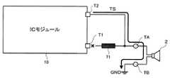
以下、図面を参照しつつ、本発明に係る実施形態を説明する。図1は、本発明の実施形態に係る信号増幅装置1の主要構成を示すブロック図である。信号増幅装置1は、IC又はICモジュールなどで構成される半導体集積回路10と、第1外部端子TA、第2外部端子TB、及び内部負荷71を備える。
第1外部端子TA及び第2外部端子TBは、例えば、ヘッドホンのジャックとプラグの接続点に相当する。第1外部端子TA及び第2外部端子TBには外部負荷2が接続される。外部負荷2としては、インピーダンスが相違するヘッドホンやスピーカなどが該当する。この例では、第1外部端子TAからテスト信号TS又は出力信号Soutが出力され、第2外部端子TBには接地電位(所定の電位)が供給される。半導体集積回路10は、テスト期間においてテスト信号TSを外部負荷2に供給し、外部負荷2のインピーダンスに応じてテスト期間以外の期間において出力信号Soutの振幅を調整するようになっている。<1. Embodiment>
Embodiments according to the present invention will be described below with reference to the drawings. FIG. 1 is a block diagram showing a main configuration of a
The first external terminal TA and the second external terminal TB correspond to a connection point between a headphone jack and a plug, for example. An
内部負荷71は、第1外部端子TAと半導体集積回路10との間に設けられており、高域周波数のノイズを除去するフェライトビーズや、大振幅の信号からスピーカやヘッドホンなどの外部負荷2を保護するための保護抵抗などを含んで構成してもよい。 The
半導体集積回路10は、内部負荷71と接続される第1端子T1と、第1外部端子TAに接続される第2端子T2とを備える。
また、半導体集積回路10は、差動形式の入力信号Sinを増幅してシングルエンド形式の出力信号Soutを生成し、第1端子T1に供給する増幅部20を備える。より具体的には、増幅部20は、第1制御信号CTL1に基づいて、入力信号Sinの振幅を調整する信号調整部21とアンプ22とを備える。この例では、アンプ22のゲインは固定であり、増幅部20のゲインは、信号調整部21によって制御される。なお、この例では、入力信号Sinを差動形式としたが、シングルエンド形式であってもよいことは勿論である。この場合、信号調整部21及びアンプ22はシングルエンド形式で構成される。The semiconductor integrated
The semiconductor integrated
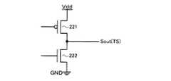
また、アンプ22には、テスト期間においてハイレベルとなり、テスト期間以外の期間においてローレベルとなる第2制御信号CTL2が供給される。アンプ22の出力段は、例えば、図2に示すようにPチャネルトランジスタ221とNチャネルトランジスタ222とが直列に接続されており、テスト期間ではPチャネルトランジスタ221のゲート電位が電源電圧Vddにプルアップされ、Nチャネルトランジスタ222のゲート電位が接地電位にプルダウンされる。一方、テスト期間以外の期間では、Pチャネルトランジスタ221及びNチャネルトランジスタ222のゲートは適切にバイアスされ、出力信号Soutが低インピーダンスで出力される。これにより、テスト期間では、増幅部20の出力インピーダンスがハイインピーダンス状態となり、テスト期間以外の期間では、増幅部20から出力信号Soutが第1外部端子TAに出力され、内部負荷71を介してヘッドホンなどの外部負荷2に供給される。 The
さらに、半導体集積回路10は、テスト信号生成部30、抵抗40、AD変換部50、及び制御部60を備える。テスト信号生成部30は、差動形式のテスト信号TSを発生する信号発生器31とアンプ32を備える。
ここで、テスト信号TSについて図3を参照して説明する。テスト信号TSは、連続する余弦波Fから1波長の波形F1を切り出した部分を含むものとなっている。より具体的には、テスト信号TSは、余弦波Fの上側ピークP1(以下、第1の上側ピークP1と称する)から次の上側ピークP2(以下、第2の上側ピークと称する)までの1波長の波形F1を切り出して、第1の上側ピークP1と第2の上側ピークP2を、出力信号Soutの振幅中心電位Vcとなるようにレベルシフトさせたものである。なお、この例では、信号発生器31で発生するテスト信号TSを差動形式としたが、シングルエンド形式であってもよいことは勿論である。この場合、信号発生器31及びアンプ32はシングルエンド形式で構成される。また、振幅中心電位Vcは、例えば、第2外部端子TBに所定の電位として供給される接地電位GNDである。Furthermore, the semiconductor integrated
Here, the test signal TS will be described with reference to FIG. The test signal TS includes a portion obtained by cutting out a waveform F1 of one wavelength from a continuous cosine wave F. More specifically, the test signal TS is 1 from the upper peak P1 of the cosine wave F (hereinafter referred to as the first upper peak P1) to the next upper peak P2 (hereinafter referred to as the second upper peak). The waveform F1 of the wavelength is cut out, and the first upper peak P1 and the second upper peak P2 are level-shifted so as to become the amplitude center potential Vc of the output signal Sout. In this example, the test signal TS generated by the
このようにテスト信号TSを生成したのは、利用者に異音を感じさせないためである。ヘッドホンやスピーカで再生しても利用者が気づかないようにするためには、1)テスト信号TSの周波数成分を可聴帯域において人の聴覚で感じられない程度に小さくすること、
2)テスト信号TSの発生時間を人の聴覚で感じられない程度に短くすることが必要である。The reason why the test signal TS is generated in this way is to prevent the user from feeling abnormal noise. In order to prevent the user from noticing even when playing back with headphones or speakers, 1) reducing the frequency component of the test signal TS to such an extent that it cannot be felt by human hearing in the audible band,
2) It is necessary to shorten the generation time of the test signal TS to such an extent that it cannot be felt by human hearing.
例えば、図4に示すようにテスト信号TSの波形を連続した余弦波とすると、その周波数成分は基本周波数fにおいて大きなエネルギーを持つため、人の聴覚で感じられ易くなる。基本周波数fのエネルギーを低くするためには、テスト信号TSの振幅を小さくすればよい。しかしながら、人の聴覚で感じられない程度にテスト信号TSの振幅を小さくすると、外部負荷2のインピーダンスを計測する際に、SN比が低下し、測定されたインピーダンスが不正確になる。
また、例えば、図5に示すようにテスト信号TSの波形を方形波にすると、テスト信号TSの周波数成分は基本周波数f及びその高調波において大きなエネルギーを持つため、人の聴覚で感じられ易くなる。For example, if the waveform of the test signal TS is a continuous cosine wave as shown in FIG. 4, the frequency component has a large energy at the fundamental frequency f, so that it is easily felt by human hearing. In order to reduce the energy of the fundamental frequency f, the amplitude of the test signal TS may be reduced. However, if the amplitude of the test signal TS is reduced to such an extent that it cannot be perceived by human hearing, when the impedance of the
Further, for example, when the waveform of the test signal TS is a square wave as shown in FIG. 5, the frequency component of the test signal TS has a large energy at the fundamental frequency f and its harmonics, so that it is easily perceived by human hearing. .
そこで、本実施形態では、テスト信号TSを余弦波から切り出した1波長F1とすることで、テスト信号TSの発生時間を短くし、且つ、高調波成分を殆ど発生しないようにしたのである。例えば、図6に示すように余弦波の半波長を切り出した波形Wと、テスト信号TSとを比較すると、肩の部分SDにおいて波形Wの方が急峻に変化していることが分かる。従って、余弦波の半波長を切り出した波形Wは高調波成分が発生するが、テスト信号TSはなだらかに変化するため、高調波成分が殆ど発生しない。
この結果、テスト信号TSのスぺクトラムは図7に示すものとなり、図4に示す余弦波が連続する場合と比較すると、大幅に基本波周波数fのエネルギーを低減することができる。しかも、発生時間が短いのでテスト信号TSの振幅Vx(図3参照)を大きく設定することができ、高いSN比で外部負荷2のインピーダンスを測定することが可能となる。
本実施形態ではテスト信号TSの基本周波数fは3Hzである。可聴帯域は20Hz〜20KHzであるので、テスト信号TSの基本周波数fは可聴帯域の最低周波数よりも低い。一般にテスト信号TSの周波数が高くなるほど、浮遊容量、浮遊インダクタンスあるいは配線抵抗の影響を受けてテスト信号TSのレベルが減衰してしまうため、外部負荷2のインピーダンスの測定誤差が大きくなる。一方、可聴帯域の最低周波数よりも低い周波数では、浮遊容量、浮遊インダクタンスあるいは配線抵抗の影響を受けてテスト信号TSが減衰することが殆どない。しかも、テスト信号TSは高調波成分が極めて小さいので、可聴帯域において異音として人が感じる高調波が発生しない。これにより、利用者が気にならないテスト信号TSを用いて、正確に外部負荷2のインピーダンスを測定することが可能となる。Therefore, in this embodiment, the test signal TS is set to one wavelength F1 cut out from the cosine wave, so that the generation time of the test signal TS is shortened and almost no harmonic component is generated. For example, as shown in FIG. 6, when the waveform W obtained by cutting out the half wavelength of the cosine wave is compared with the test signal TS, it can be seen that the waveform W changes more rapidly in the shoulder portion SD. Therefore, the waveform W obtained by cutting out the half wavelength of the cosine wave generates a harmonic component, but the test signal TS changes gently, so that almost no harmonic component is generated.
As a result, the spectrum of the test signal TS is as shown in FIG. 7, and the energy of the fundamental frequency f can be greatly reduced as compared with the case where the cosine wave shown in FIG. 4 continues. Moreover, since the generation time is short, the amplitude Vx (see FIG. 3) of the test signal TS can be set large, and the impedance of the
In the present embodiment, the basic frequency f of the test signal TS is 3 Hz. Since the audible band is 20 Hz to 20 KHz, the basic frequency f of the test signal TS is lower than the lowest frequency of the audible band. Generally, the higher the frequency of the test signal TS, the more the measurement error of the impedance of the
説明を図1に戻す。次に、アンプ32は、所定のゲインでテスト信号TSを増幅して、抵抗40に供給する。また、アンプ32の出力段は、アンプ22と同様に、例えば、図2に示すように構成されている。そして、第2制御信号CTL2がハイレベルとなるテスト期間において、Pチャネルトランジスタ221及びNチャネルトランジスタ222のゲートは適切にバイアスされ、第2制御信号CTL2がローレベルとなるテスト期間以外の期間においてオフ状態となるように構成されている。これにより、テスト期間ではテスト信号生成部30からテスト信号TSが、抵抗40を介してヘッドホンなどの外部負荷2に供給され、テスト期間以外の期間では、テスト信号生成部30の出力側がハイインピーダンス状態になることに伴って第2端子T2がハイインピーダンス状態となる。 Returning to FIG. Next, the
次に、AD変換部50は、第2端子T2の電位をAD変換して得た検出データDを制御部60に出力する。即ち、AD変換部50は、テスト期間において第2端子T2におけるテスト信号TSの振幅を検出する検出部として機能する。 Next, the
次に、制御部60には、外部装置から第1外部端子TA及び第2外部端子TBにヘッドホンなどの外部負荷2が接続されるとアクティブになる検知信号CTLが供給される。制御部60は、検知信号CTLがアクティブになった後、所定時間だけ第2制御信号CTL2をハイレベルとする。第2制御信号CTL2がハイレベルの期間がテスト期間となる。
そして、テスト期間における検出データDに基づいて、外部負荷2のインピーダンスを測定し、外部負荷2のインピーダンスに応じて第1制御信号CTL1を生成する。より具体的は、図3に示すようにテスト信号TSの振幅が最大(信号レベルが最小)となる時刻Txにおける検出データDに基づいて、インピーダンスを算出すればよい。Next, a detection signal CTL that is activated when an
Then, based on the detection data D in the test period, the impedance of the
信号発生器31で生成するテスト信号TSの振幅は既知であり、アンプ32のゲインも既知である。従って、テスト信号生成部30から出力されるテスト信号TSの振幅も既知である。ここで、テスト信号生成部30から出力されるテスト信号TSの振幅をV2、第2端子におけるテスト信号TSの振幅をV1、抵抗40のインピーダンスをZy、外部負荷2のインピーダンスをZxとすれば、外部負荷2のインピーダンスZxは、以下に示す式(1)で与えられる。
Zx=ZyV1/(V2−V1)…(1)The amplitude of the test signal TS generated by the
Zx = ZyV1 / (V2-V1) (1)
制御部60は、式(1)に従ってインピーダンスZxを算出し、インピーダンスZxに応じた第1制御信号CTL1を生成し、増幅部20のゲインを調整する。この結果、異なる種類の外部負荷2が接続されても、適切な音量を出力することができる。 The
本実施形態によれば、テスト期間以外の期間では、図8に示すように第1端子T1から出力される出力信号Soutが内部負荷71を介して外部負荷2に供給される一方、第2端子T2はハイインピーダンス状態となる。従って、テスト信号TSと独立して出力信号Soutを外部負荷2に供給することができる。また、内部負荷71を介して出力信号Soutを供給するので、外部負荷2が故障などの理由で短絡したとしても、半導体集積回路10を保護することができ、更に、大振幅の出力信号Soutが半導体集積回路10から出力されても外部負荷2を保護することができる。 According to the present embodiment, in a period other than the test period, the output signal Sout output from the first terminal T1 is supplied to the
次に、テスト期間では、図9に示すように第1端子T1はハイインピーダンス状態となる一方、第2端子T2から出力されるテスト信号TSは内部負荷71を通らずに、外部負荷2に直接供給される。この結果、内部負荷71の影響を受けることなく、外部負荷2のインピーダンスを正確に特定することができ、異なる種類の外部負荷2が接続されても、適切な音量を出力することが可能となる。 Next, in the test period, as shown in FIG. 9, the first terminal T1 is in a high impedance state, while the test signal TS output from the second terminal T2 does not pass through the
<2.変形例>
本発明は、上述した実施形態に限定されるものではなく、例えば、以下に述べる各種の変形が可能である。また、上述した実施形態と各変形例は適宜組み合わせてもよいことは勿論である。<2. Modification>
The present invention is not limited to the above-described embodiments, and for example, various modifications described below are possible. Of course, the above-described embodiment and each modification may be appropriately combined.
(1)上述した実施形態では、振幅中心電位Vcを基準として負側にピークを有するテスト信号TSを一例として説明したが、本発明は、これに限定されるものではなく、テスト信号TSは、余弦波の1波長を切り出した波形であれば、どのタイミングで切り出してもよい。例えば、テスト信号TSを、図10に示すように余弦波Fの下側ピークP3(以下、第1の下側ピークP3と称する)から次の下側ピークP4(以下、第2の下側ピークP4と称する)までの1波長の波形F1を切り出して、第1の下側ピークP3と第2の下側ピークP4を、出力信号Soutの振幅中心電位Vcとなるようにレベルシフトさせた波形としてもよい。
また、上述した実施形態においては、テスト信号TSの基本周波数fを可聴帯域の最低周波数である20Hzよりも小さく設定したが、本発明はこれに限定されるものではなく、利用者に気づかれないのであれば、テスト信号TSの周波数をどのように設定してもよい。但し、テスト信号TSの減衰を考慮して、可聴帯域の最高周波数である20KHzよりも低いことが好ましい。
加えて、上述した実施形態では可聴帯域を20Hz〜20KHzとしたが、信号増幅回路1の使用目的によって可聴帯域は相違する。例えば、電話においては、可聴帯域が300Hz〜3.5KHzあるいは、100Hz〜7KHzとなる。(1) In the above-described embodiment, the test signal TS having a peak on the negative side with respect to the amplitude center potential Vc has been described as an example. However, the present invention is not limited to this, and the test signal TS is As long as the waveform is obtained by cutting out one wavelength of the cosine wave, it may be cut out at any timing. For example, the test signal TS is changed from the lower peak P3 of the cosine wave F (hereinafter referred to as the first lower peak P3) to the next lower peak P4 (hereinafter referred to as the second lower peak) as shown in FIG. A waveform F1 of one wavelength up to P4) is cut out, and the first lower peak P3 and the second lower peak P4 are level-shifted so as to be the amplitude center potential Vc of the output signal Sout. Also good.
In the above-described embodiment, the basic frequency f of the test signal TS is set to be lower than 20 Hz, which is the lowest frequency of the audible band. However, the present invention is not limited to this and is not noticed by the user. In this case, the frequency of the test signal TS may be set in any way. However, in consideration of the attenuation of the test signal TS, it is preferably lower than 20 KHz which is the highest frequency of the audible band.
In addition, although the audible band is 20 Hz to 20 KHz in the above-described embodiment, the audible band is different depending on the purpose of use of the
(2)上述した実施形態では、半導体集積回路10に第2端子T2が設けられており、第2端子T2と第1外部端子TAと接続して、内部負荷71を迂回してテスト信号TSを外部負荷2に供給したが、本発明はこれに限定されるものではなく、テスト期間において外部負荷2にテスト信号TSを供給し、テスト期間以外の期間において外部負荷2に出力信号Soutを供給するのであれば、どのような構成であってもよい。
例えば、図11に示す信号増幅回路1Zのように、半導体集積回路10Zには第2端子T2が設けられておらず、抵抗40が第1端子T1に接続されているものであってもよい。この場合には、テスト信号TSが内部負荷71を介して外部負荷2に供給される。内部負荷71の大きさが小さい場合には、この変形例においても、外部負荷2のインピーダンスを必要な精度で測定することが可能である。また、内部負荷71の大きさが既知であれば、これを考慮して、外部負荷2のインピーダンスを計測してもよい。
この場合にもテスト信号TSとして余弦波の1波長F1を切り出したものを用いるので、テスト信号TSをヘッドホンやスピーカなどに供給しても、利用者に気づかれないようにできる。(2) In the above-described embodiment, the semiconductor integrated
For example, like the
Also in this case, since the test signal TS obtained by cutting out one wavelength F1 of the cosine wave is used, even if the test signal TS is supplied to headphones, a speaker, etc., it is possible to prevent the user from being noticed.
(3)上述した実施形態では、テスト信号生成部30から出力されるテスト信号TSの振幅V2は既知であるとしたが、本発明はこれに限定されるものではなく、テスト信号生成部30から出力されるテスト信号TSの振幅V2を測定して外部負荷2のインピーダンスを特定してもよい。(3) In the above-described embodiment, the amplitude V2 of the test signal TS output from the test
例えば、図12に示す半導体集積回路10Aを用いて、信号増幅装置1を構成してもよい。この場合、テスト信号生成部30から出力されるテスト信号TSの振幅V2をAD変換して検出データDaを出力するAD変換部50Aと、第2端子T2におけるテスト信号TSの振幅V1をAD変換して検出データDbを出力するAD変換部50Bを設け、制御部60は、検出データDa及び検出データDbに基づいて、外部負荷2のインピーダンスを特定すればよい。 For example, the
このように、テスト信号TSの振幅V2を測定すると、テスト信号生成部30の製造ばらつき、温度特性、あるいは経時変化によってテスト信号TSの振幅V2が変化しても、これを実測するので、より正確に外部負荷2のインピーダンスを測定することができる。 As described above, when the amplitude V2 of the test signal TS is measured, even if the amplitude V2 of the test signal TS changes due to manufacturing variations, temperature characteristics, or changes over time of the test
(4)上述した実施形態及び変形例では、制御部60は、式(1)に基づいて外部負荷2のインピーダンスを算出することとしたが、本発明はこれに限定されるものではなく、第2端子T2におけるテスト信号TSの振幅V1に基づいて、第1制御信号CTL1を生成してもよい。テスト信号生成部30から出力されるテスト信号TSの振幅V2は固定であるので、外部負荷2のインピーダンスと第2端子T2におけるテスト信号TSの振幅V1とは、1対1に対応する。そして、外部負荷2のインピーダンスに応じて増幅部20のゲインを決定するので、予めテスト信号TSの振幅V1と増幅部20のゲインの関係を定めておけば、インピーダンスを算出しなくても、第1制御信号CTL1を直接生成することができる。具体的には、テスト信号TSの振幅V1と第1制御信号CTL1の大きさとをテーブルに記憶しておき、テーブルを参照して第1制御信号CTL1を生成すればよい。(4) In the embodiment and the modification described above, the
(5)上述した実施形態では、2極タイプのプラグについて説明したが、3極又は4極タイプのプラグに適用してもよいことは勿論である。ところで、4極タイプのプラグは、先端から、Lch、Rch、GND、MICが配置される第1態様と、先端からLch、Rch、MIC、GNDが配置される第2態様が存在する。この場合、先端から3番目の電極に、第1態様ではGNDが接続される一方、第2態様ではMICが接続される。上述した実施形態を4極タイプのプラグに適用した場合には、先端から3番目の電極のインピーダンスを算出することによって、第1態様と第2態様とを判別することができる。第1態様ではGNDと接続されるためインピーダンスはゼロとなるが、第2態様ではマイクが接続されるため、マイクのインピーダンスが算出される。したがって、インピーダンスに基づいてプラグの種類を判別することが可能となる。(5) Although the two-pole type plug has been described in the above-described embodiment, it is needless to say that the present invention may be applied to a three-pole or four-pole type plug. By the way, the 4-pole type plug has a first mode in which Lch, Rch, GND, and MIC are arranged from the tip, and a second mode in which Lch, Rch, MIC, and GND are arranged from the tip. In this case, the GND is connected to the third electrode from the tip in the first mode, while the MIC is connected in the second mode. When the above-described embodiment is applied to a four-pole type plug, the first mode and the second mode can be determined by calculating the impedance of the third electrode from the tip. In the first mode, the impedance is zero because it is connected to GND, but in the second mode, a microphone is connected, so the impedance of the microphone is calculated. Therefore, the type of plug can be determined based on the impedance.
1,1Z……信号増幅装置、2……外部負荷、10,10A,10Z……半導体集積回路、20……増幅部、21……信号調整部、22……アンプ、30……テスト信号生成部、31……信号発生器、32……アンプ、40……抵抗、50……AD変換部、60……制御部、71……内部負荷、TA……第1外部端子、TB……第2外部端子、T1……第1端子、T2……第2端子、Sin……入力信号、Sout……出力信号、CTL1……第1制御信号、CTL2……第2制御信号。
DESCRIPTION OF
Claims (8)
Translated fromJapanese一端が第2端子に接続された抵抗と、
テスト信号を生成して前記抵抗の他端に供給するテスト信号生成部と、
前記第2端子における前記テスト信号の振幅を検出する検出部と、
前記増幅部及び前記テスト信号生成部の出力を制御する制御部とを備え、
前記テスト信号生成部は、余弦波の1波長の波形を前記テスト信号として生成し、
前記テスト信号の周波数は、可聴帯域の最低周波数よりも低い、
ことを特徴とする半導体集積回路。An amplifying section for outputtingan output signal by amplifying theinput signal to thefirst terminal,
A resistor having one end connected tothe second terminal;
A test signal generation unit that generates a test signal and supplies the test signal to the other end of the resistor;
A detector for detecting the amplitude of the test signal at the second terminal;
A control unit for controlling the output of the amplification unit and the test signal generation unit,
The test signal generation unit generates a waveform of one wavelength of a cosine wave as the test signal,
The frequency of the test signal is lower than the lowest frequency of the audible band;
A semiconductor integrated circuit.
一端が前記第1端子に接続された抵抗と、A resistor having one end connected to the first terminal;
テスト信号を生成して前記抵抗の他端に供給するテスト信号生成部と、A test signal generation unit that generates a test signal and supplies the test signal to the other end of the resistor;
前記第1端子における前記テスト信号の振幅を検出する検出部と、A detector for detecting the amplitude of the test signal at the first terminal;
前記増幅部及び前記テスト信号生成部の出力を制御する制御部とを備え、A control unit for controlling the output of the amplification unit and the test signal generation unit,
前記テスト信号生成部は、余弦波の1波長の波形を前記テスト信号として生成し、The test signal generation unit generates a waveform of one wavelength of a cosine wave as the test signal,
前記テスト信号の周波数は、可聴帯域の最低周波数よりも低い、The frequency of the test signal is lower than the lowest frequency of the audible band;
ことを特徴とする半導体集積回路。A semiconductor integrated circuit.
テスト期間において、前記テスト信号を出力するように前記テスト信号生成部を制御するとともに、出力インピーダンスをハイインピーダンス状態とするように前記増幅部を制御し、
前記テスト期間以外の期間において、出力インピーダンスをハイインピーダンス状態とするように前記テスト信号生成部を制御するとともに、前記出力信号を出力するように前記増幅部を制御する、
ことを特徴とする請求項1乃至3のうちいずれか1項に記載の半導体集積回路。The controller is
In the test period, the test signal generator is controlled to output the test signal, and the amplifier is controlled so that the output impedance is in a high impedance state.
In a period other than the test period, the test signal generation unit is controlled to set the output impedance to a high impedance state, and the amplification unit is controlled to output the output signal.
The semiconductor integrated circuit accordingto any one of claims 1 to 3 .
所定の電位が供給される第2外部端子と、A second external terminal to which a predetermined potential is supplied;
一端が前記第1外部端子に接続された内部負荷と、An internal load having one end connected to the first external terminal;
入力信号を増幅して出力信号を前記内部負荷の他端に出力する増幅部と、An amplifier for amplifying an input signal and outputting an output signal to the other end of the internal load;
一端が前記第1外部端子に接続された抵抗と、A resistor having one end connected to the first external terminal;
テスト信号を生成して前記抵抗の他端に供給するテスト信号生成部と、A test signal generation unit that generates a test signal and supplies the test signal to the other end of the resistor;
前記第1外部端子における前記テスト信号の振幅を検出する検出部と、A detection unit for detecting the amplitude of the test signal at the first external terminal;
前記増幅部及び前記テスト信号生成部の出力を制御する制御部とを備え、A control unit for controlling the output of the amplification unit and the test signal generation unit,
前記テスト信号生成部は、余弦波の1波長の波形を前記テスト信号として生成し、The test signal generation unit generates a waveform of one wavelength of a cosine wave as the test signal,
前記テスト信号の周波数は、可聴帯域の最低周波数よりも低い、The frequency of the test signal is lower than the lowest frequency of the audible band;
ことを特徴とする信号増幅装置。A signal amplifying device.
所定の電位が供給される第2外部端子と、A second external terminal to which a predetermined potential is supplied;
一端が前記第1外部端子に接続された内部負荷と、An internal load having one end connected to the first external terminal;
入力信号を増幅して出力信号を前記内部負荷の他端に出力する増幅部と、An amplifier for amplifying an input signal and outputting an output signal to the other end of the internal load;
一端が前記内部負荷の他端に接続された抵抗と、A resistor having one end connected to the other end of the internal load;
テスト信号を生成して前記抵抗の他端に供給するテスト信号生成部と、A test signal generation unit that generates a test signal and supplies the test signal to the other end of the resistor;
前記内部負荷の他端における前記テスト信号の振幅を検出する検出部と、A detector for detecting the amplitude of the test signal at the other end of the internal load;
前記増幅部及び前記テスト信号生成部の出力を制御する制御部とを備え、A control unit for controlling the output of the amplification unit and the test signal generation unit,
前記テスト信号生成部は、余弦波の1波長の波形を前記テスト信号として生成し、The test signal generation unit generates a waveform of one wavelength of a cosine wave as the test signal,
前記テスト信号の周波数は、可聴帯域の最低周波数よりも低い、The frequency of the test signal is lower than the lowest frequency of the audible band;
ことを特徴とする信号増幅装置。A signal amplifying device.
Priority Applications (3)
| Application Number | Priority Date | Filing Date | Title |
|---|---|---|---|
| JP2012113384AJP5924116B2 (en) | 2012-05-17 | 2012-05-17 | Semiconductor integrated circuit and signal amplifier |
| US13/895,837US9535102B2 (en) | 2012-05-17 | 2013-05-16 | Test signal supplying device and semiconductor integrated circuit |
| CN201310184666.2ACN103424625B (en) | 2012-05-17 | 2013-05-17 | Test signal supply equipment and SIC (semiconductor integrated circuit) |
Applications Claiming Priority (1)
| Application Number | Priority Date | Filing Date | Title |
|---|---|---|---|
| JP2012113384AJP5924116B2 (en) | 2012-05-17 | 2012-05-17 | Semiconductor integrated circuit and signal amplifier |
Publications (3)
| Publication Number | Publication Date |
|---|---|
| JP2013240008A JP2013240008A (en) | 2013-11-28 |
| JP2013240008A5 JP2013240008A5 (en) | 2015-04-23 |
| JP5924116B2true JP5924116B2 (en) | 2016-05-25 |
Family
ID=49764661
Family Applications (1)
| Application Number | Title | Priority Date | Filing Date |
|---|---|---|---|
| JP2012113384AActiveJP5924116B2 (en) | 2012-05-17 | 2012-05-17 | Semiconductor integrated circuit and signal amplifier |
Country Status (1)
| Country | Link |
|---|---|
| JP (1) | JP5924116B2 (en) |
Families Citing this family (1)
| Publication number | Priority date | Publication date | Assignee | Title |
|---|---|---|---|---|
| CN106162489B (en) | 2015-03-27 | 2019-05-10 | 华为技术有限公司 | A kind of earphone state detection method and terminal |
Family Cites Families (12)
| Publication number | Priority date | Publication date | Assignee | Title |
|---|---|---|---|---|
| JPH10327026A (en)* | 1997-05-23 | 1998-12-08 | Nippon Columbia Co Ltd | Amplifier |
| JPH11355880A (en)* | 1998-06-12 | 1999-12-24 | Sharp Corp | Sound reproduction device |
| US7890284B2 (en)* | 2002-06-24 | 2011-02-15 | Analog Devices, Inc. | Identification system and method for recognizing any one of a number of different types of devices |
| JP4182802B2 (en)* | 2003-04-25 | 2008-11-19 | ソニー株式会社 | Acoustic signal input / output device, input / output circuit switching method |
| JP4279210B2 (en)* | 2004-06-24 | 2009-06-17 | パイオニア株式会社 | High frequency signal output delay time adjustment device |
| JP4692084B2 (en)* | 2005-06-06 | 2011-06-01 | 富士電機システムズ株式会社 | Analog input overvoltage protection circuit |
| KR100788670B1 (en)* | 2005-11-03 | 2007-12-26 | 삼성전자주식회사 | Method and device for controlling output power of digital amplifier optimized for headphones |
| EP2229006B2 (en)* | 2008-01-10 | 2019-02-27 | Toa Corporation | Speaker line inspection device |
| US9014396B2 (en)* | 2008-01-31 | 2015-04-21 | Qualcomm Incorporated | System and method of reducing click and pop noise in audio playback devices |
| JP2009296478A (en)* | 2008-06-09 | 2009-12-17 | Oki Semiconductor Co Ltd | Amplification circuit |
| JP5515728B2 (en)* | 2009-12-24 | 2014-06-11 | ブラザー工業株式会社 | Terminal device, processing method, and processing program |
| JP2013131910A (en)* | 2011-12-21 | 2013-07-04 | Sharp Corp | Voice output device |
- 2012
- 2012-05-17JPJP2012113384Apatent/JP5924116B2/enactiveActive
Also Published As
| Publication number | Publication date |
|---|---|
| JP2013240008A (en) | 2013-11-28 |
Similar Documents
| Publication | Publication Date | Title |
|---|---|---|
| CN104735600B (en) | Loudspeaker controller | |
| CN106063124B (en) | For detecting the system and method for being coupled to the load impedance of transducer device of audio frequency apparatus | |
| CN107078707B (en) | System and method for gain calibration of audio signal paths | |
| JP6082008B2 (en) | Audio signal processing method and audio signal processing apparatus using the same | |
| CN101656901B (en) | Noise-canceling system | |
| TWI511579B (en) | Headphone with active noise cancelling and auto-calibration method thereof | |
| US10045124B2 (en) | Crosstalk mitigation | |
| US9438982B2 (en) | Systems and methods for detection of load impedance of a transducer device coupled to an audio device | |
| US8358788B2 (en) | Noise cancellation for microphone-speaker combinations using combined speaker amplifier and reference sensing | |
| TW201501544A (en) | Control circuit for audio outputting of earphone | |
| TWI713374B (en) | Audio adjustment method and associated audio adjustment device for active noise cancellation | |
| US11070179B2 (en) | Apparatus and method for measuring speaker transducer impedance versus frequency with ultralow inaudible signal | |
| US9535102B2 (en) | Test signal supplying device and semiconductor integrated circuit | |
| US20130082691A1 (en) | Headset and earphone | |
| JP5924116B2 (en) | Semiconductor integrated circuit and signal amplifier | |
| JP6872383B2 (en) | A device for measuring the current generated by an acoustic amplifier to operate an acoustic speaker | |
| TW595238B (en) | Feedback type active noise control circuit | |
| JP2013240007A (en) | Semiconductor integrated circuit and signal amplifying device | |
| JP6197593B2 (en) | Signal processing device | |
| US8488801B2 (en) | Audio compensation unit and compensating method and audio processing device thereof | |
| US9225301B2 (en) | Amplifier apparatus with controlled negative output impedance | |
| JP2013240008A5 (en) | ||
| TWI880434B (en) | Device and method for estimating temperature of speaker voice coil | |
| CN211352416U (en) | a headphone | |
| CN120567054A (en) | Sound masking effect-based sound explosion suppression method for audio amplifier |
Legal Events
| Date | Code | Title | Description |
|---|---|---|---|
| A521 | Request for written amendment filed | Free format text:JAPANESE INTERMEDIATE CODE: A523 Effective date:20150310 | |
| A621 | Written request for application examination | Free format text:JAPANESE INTERMEDIATE CODE: A621 Effective date:20150324 | |
| A621 | Written request for application examination | Free format text:JAPANESE INTERMEDIATE CODE: A621 Effective date:20150324 | |
| RD04 | Notification of resignation of power of attorney | Free format text:JAPANESE INTERMEDIATE CODE: A7424 Effective date:20150410 | |
| A977 | Report on retrieval | Free format text:JAPANESE INTERMEDIATE CODE: A971007 Effective date:20150806 | |
| A131 | Notification of reasons for refusal | Free format text:JAPANESE INTERMEDIATE CODE: A131 Effective date:20150818 | |
| A521 | Request for written amendment filed | Free format text:JAPANESE INTERMEDIATE CODE: A523 Effective date:20151014 | |
| TRDD | Decision of grant or rejection written | ||
| A01 | Written decision to grant a patent or to grant a registration (utility model) | Free format text:JAPANESE INTERMEDIATE CODE: A01 Effective date:20160322 | |
| A61 | First payment of annual fees (during grant procedure) | Free format text:JAPANESE INTERMEDIATE CODE: A61 Effective date:20160404 | |
| R151 | Written notification of patent or utility model registration | Ref document number:5924116 Country of ref document:JP Free format text:JAPANESE INTERMEDIATE CODE: R151 | |
| S531 | Written request for registration of change of domicile | Free format text:JAPANESE INTERMEDIATE CODE: R313532 | |
| R350 | Written notification of registration of transfer | Free format text:JAPANESE INTERMEDIATE CODE: R350 |