JP5924088B2 - Optical transmission system - Google Patents
Optical transmission systemDownload PDFInfo
- Publication number
- JP5924088B2 JP5924088B2JP2012087975AJP2012087975AJP5924088B2JP 5924088 B2JP5924088 B2JP 5924088B2JP 2012087975 AJP2012087975 AJP 2012087975AJP 2012087975 AJP2012087975 AJP 2012087975AJP 5924088 B2JP5924088 B2JP 5924088B2
- Authority
- JP
- Japan
- Prior art keywords
- frequency
- multiplex
- band
- data signal
- signal
- Prior art date
- Legal status (The legal status is an assumption and is not a legal conclusion. Google has not performed a legal analysis and makes no representation as to the accuracy of the status listed.)
- Expired - Fee Related
Links
Images


Classifications
- H—ELECTRICITY
- H04—ELECTRIC COMMUNICATION TECHNIQUE
- H04J—MULTIPLEX COMMUNICATION
- H04J14/00—Optical multiplex systems
- H04J14/02—Wavelength-division multiplex systems
- H—ELECTRICITY
- H04—ELECTRIC COMMUNICATION TECHNIQUE
- H04J—MULTIPLEX COMMUNICATION
- H04J14/00—Optical multiplex systems
- H04J14/02—Wavelength-division multiplex systems
- H04J14/0227—Operation, administration, maintenance or provisioning [OAMP] of WDM networks, e.g. media access, routing or wavelength allocation
- H04J14/0254—Optical medium access
- H04J14/0256—Optical medium access at the optical channel layer
- H—ELECTRICITY
- H04—ELECTRIC COMMUNICATION TECHNIQUE
- H04J—MULTIPLEX COMMUNICATION
- H04J14/00—Optical multiplex systems
- H04J14/02—Wavelength-division multiplex systems
- H04J14/0298—Wavelength-division multiplex systems with sub-carrier multiplexing [SCM]
- H—ELECTRICITY
- H04—ELECTRIC COMMUNICATION TECHNIQUE
- H04L—TRANSMISSION OF DIGITAL INFORMATION, e.g. TELEGRAPHIC COMMUNICATION
- H04L5/00—Arrangements affording multiple use of the transmission path
- H04L5/003—Arrangements for allocating sub-channels of the transmission path
Landscapes
- Engineering & Computer Science (AREA)
- Signal Processing (AREA)
- Computer Networks & Wireless Communication (AREA)
- Optical Communication System (AREA)
- Optical Modulation, Optical Deflection, Nonlinear Optics, Optical Demodulation, Optical Logic Elements (AREA)
Description
Translated fromJapanese本件は、光伝送システムに関する。 The present case relates to an optical transmission system.
複数の送信装置において、電気信号を、それぞれ異なる周波数の光信号に変調し、共通の搬送光に多重して受信装置に伝送する光周波数分割多重(FDM:Frequency Division Multiplexing)技術が知られている(特許文献1参照)。この技術によると、単一周波数の搬送光と、各多重送信装置により生成された各周波数の光変調信号とを、相互位相変調(XPM:Cross Phase Modulation)させることより、搬送光を介して複数のデータ信号を受信端に送信することができる。 2. Description of the Related Art An optical frequency division multiplexing (FDM) technique that modulates electrical signals into optical signals of different frequencies and multiplexes them with a common carrier light and transmits them to a receiver in a plurality of transmitters is known. (See Patent Document 1). According to this technique, a single frequency carrier light and an optical modulation signal of each frequency generated by each multiplex transmission device are subjected to cross-phase modulation (XPM), so that a plurality of signals are transmitted via the carrier light. Can be transmitted to the receiving end.
一方、受信装置は、搬送光を受けて電気信号に変換した後、電気フィルタにより各データ信号を抽出する。したがって、受信装置は、変換前の光信号の状態において各データ信号を抽出する場合とは異なり、各送信装置間、及び波長分離器において高精度な波長制御を行うことがないため、高密度に多重化された複数のデータ信号を容易に抽出することができる。この光FDM技術により、複数の送信ノードに入力された映像情報、音声情報、センサ情報、無線通信情報などの複数種類のデータ信号を、単一の伝送路を介して受信ノードに送信し、該受信ノードにおいて各データ信号を取り出すことが可能となる。 On the other hand, the receiving device receives the carrier light and converts it into an electrical signal, and then extracts each data signal using an electrical filter. Therefore, unlike the case of extracting each data signal in the state of the optical signal before the conversion, the receiving apparatus does not perform highly accurate wavelength control between the transmitting apparatuses and in the wavelength separator, so the density is high. A plurality of multiplexed data signals can be easily extracted. With this optical FDM technology, multiple types of data signals such as video information, audio information, sensor information, and wireless communication information input to a plurality of transmission nodes are transmitted to a reception node via a single transmission path, Each data signal can be taken out at the receiving node.
上記の光FDM技術に基づく光伝送システムによると、広帯域な非線形光学媒質により生ずる相互位相変調を利用するため、テラヘルツ(THz)レベルの広い周波数帯域を確保することが可能である。しかし、多重可能なデータ信号の数は、変調可能な周波数帯域の上限値、及び、各データ信号が占有する帯域幅に応じて制限される。このため、広い周波数帯域が存在していても、各データ信号に割り当て可能な周波数は制限される。 According to the optical transmission system based on the optical FDM technique, it is possible to secure a wide frequency band of terahertz (THz) level because the cross-phase modulation generated by the broadband nonlinear optical medium is used. However, the number of data signals that can be multiplexed is limited according to the upper limit value of the frequency band that can be modulated and the bandwidth that each data signal occupies. For this reason, even if a wide frequency band exists, the frequency that can be assigned to each data signal is limited.
そこで本件は上記の課題に鑑みてなされたものであり、周波数帯域を効率的に利用可能な光伝送システムを提供することを目的とする。 Therefore, the present invention has been made in view of the above problems, and an object thereof is to provide an optical transmission system that can efficiently use a frequency band.
本明細書に記載の光伝送システムは、搬送光の伝送路に設けられた複数の非線形光学媒質に、互いに異なる周波数のデータ信号を光変調器により変調してそれぞれ入力することによって、前記データ信号を前記搬送光に多重する複数の多重送信装置と、前記伝送路から入力された前記搬送光を光電変換することにより、前記複数の多重送信装置により多重された前記データ信号の各々を受信する受信装置と、前記複数の多重送信装置のうち、1つの多重送信装置の前記データ信号に使用される帯域幅の2倍の帯域内には、他の多重送信装置の前記データ信号の前記周波数が割り当てられず、前記データ信号に割り当て済みの前記周波数の2倍の周波数が使用されないように、前記複数の多重送信装置の各々の前記光変調器に共通する変調帯域に基づいて利用周波数帯域を特定し、前記利用周波数帯域において、前記データ信号の前記周波数の割り当てを管理する管理装置とを有する。In the optical transmission system described in this specification, data signals having different frequencies are modulated by an optical modulator and input to a plurality of nonlinear optical media provided in a transmission path of carrier light. And a plurality of multiplex transmitters for multiplexing the carrier light, and receiving each of the data signals multiplexed by the plurality of multiplex transmitters by photoelectrically converting the carrier light input from the transmission path And thefrequency of the data signal of another multiplex transmission device is allocated within a band twice the bandwidth used for the data signal of one multiplex transmission device among the plurality of multiplex transmission devices is not, the data signal as twice the frequency of the allocated the frequencies is not used, the modulation bandcommon to the optical modulatorof each of the plurality of multiplexing transmission apparatus Based identify usage frequency band, in the frequency band to be used, with a management device and which manages the allocation of the frequency of the data signal.
本明細書に記載の送信装置、受信装置、光伝送システムは、周波数帯域を効率的に利用できるという効果を奏する。 The transmission device, the reception device, and the optical transmission system described in this specification have an effect that the frequency band can be efficiently used.
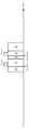
図1は、第1実施例に係る光伝送システムの構成図である。光伝送システム1は、搬送光源10と、複数の多重送信装置(1)〜(n)2と、受信ノードNとを含み、受信ノードNは、受信装置3と、管理装置4とを含む。搬送光源10と、複数の多重送信装置(1)〜(n)とは、共通の伝送路を構成する光ファイバにより互いに接続されている。また、管理装置4は、該光ファイバとは異なる伝送路の通信ネットワークNWを介して、各多重送信装置(1)〜(n)2と接続されている。 FIG. 1 is a configuration diagram of an optical transmission system according to the first embodiment. The
複数の多重送信装置(1)〜(n)2は、外部の複数のデータ信号源(1)〜(n)9からそれぞれデータ信号S1〜Snが入力される。データ信号S1〜Snとしては、例えばイーサネット(登録商標)などのデータ信号、またはセンサ装置からの検出信号が挙げられるが、限定はない。 The plurality of multiplex transmission devices (1) to (n) 2 receive data signals S1 to Sn from a plurality of external data signal sources (1) to (n) 9, respectively. Examples of the data signals S1 to Sn include a data signal such as Ethernet (registered trademark) or a detection signal from a sensor device, but are not limited thereto.
光伝送システム1は、光周波数分割多重システム(光FDM)技術に従って、搬送光源10の搬送光νcに、各多重送信装置(1)〜(n)2によって周波数f1〜fnに変調されたデータ信号S1〜Snを多重する(グラフG0〜G3参照)。データ信号S1〜Snは、受信装置3において、周波数成分f1〜fnごと抽出され、受信される。 The
図2は、第1実施例の多重送信装置(1)〜(n)2の構成図である。多重送信装置2は、変調信号生成部20と、合波器21と、非線形光学媒質22と、分波器23と、終端器24と、制御部25と、記憶部26と、通信処理部27と、選択回路28と含む。 FIG. 2 is a configuration diagram of the multiplex transmission apparatuses (1) to (n) 2 of the first embodiment. The
データ信号源(i)(i=1〜n、以下同様)9からのデータ信号Siは、選択回路28を介して変調信号生成部20に入力される。選択回路28は、制御部25から制御信号REQiが入力されている場合、信号REQiを、データ信号Siより優先して変調信号生成部20に出力する。すなわち、選択回路28は、信号REQi、及びデータ信号Siの一方を選択して変調信号生成部20に出力する。なお、信号REQiは、管理装置4に周波数の割り当てを要求する要求信号である。 The data signal Si from the data signal source (i) (i = 1 to n, the same applies hereinafter) 9 is input to the modulation
変調信号生成部20は、光変調器200と、増幅器201と、乗算器203と、低周波フィルタ204と、調整回路205と、発振器206とを含む。調整回路205は、上記の出力信号Si,REQiの振幅、及びバイアス電圧を調整する。低周波フィルタ204は、例えばRC回路であり、出力信号Si,REQiの高周波成分を除去する。 The modulation
乗算器203は、例えばミキサ回路であり、出力信号Si,REQiを、発振器206から入力された周波数fiの信号に基づいて変調する。発振器206は、例えば電圧制御発振器(VCO:Voltage Controlled Oscillator)である。制御部25は、発振器206の制御電圧Vを設定することによって、発振器206の周波数fiを制御する。
制御部25は、例えばCPU(Central Processing Unit)などの演算処理回路であり、所定のプログラムに基づいて処理を行う。なお、制御部25は、このようにソフトウェアにより機能するものに限定されることはなく、特定用途向け集積回路などのハードウェアにより機能するものであってもよい。 The
また、記憶部26は、メモリなどの記憶手段である。記憶部26は、制御部25を動作させるプログラムなどを記憶する。 The
制御部25は、通信処理を行う通信処理部27を介して外部の装置と通信する。制御部25は、操作端末(図示せず)から受信した指示信号COM、または、管理装置4から受信した信号RESに従って動作する。信号RESは、要求信号REQiに対する応答信号である。例えば、制御部25は、新たにデータ信号Siを多重する場合、指示信号COMに応じ、周波数fiの割り当てを要求する要求信号REQiを、管理装置4に送信する。このとき、制御部25は、要求信号REQiを送信するため、発振器206に固定周波数f0に対応する電圧Vを与える。 The
要求信号REQiは、データ信号Siの速度(つまり、ビットレート)に基づく帯域幅Bwiの情報を含む。管理装置4は、要求信号REQiに応じて、周波数の割り当てを行い、当該周波数fiの情報を含む応答信号RESを、通信ネットワークNWを介して多重送信装置2に送信する。そして、制御部25は、該応答信号RESが示す周波数fiに対応する電圧Vを、発振器206に印加する。これにより、データ信号Siに割り当てられる周波数fiが設定される。なお、応答信号RESは、例えば、送信先の多重送信装置(i)2を特定する宛先情報を含み、これにより、多重送信装置(i)2は、該宛先情報を参照して、自装置宛ての応答信号RESのみを処理する。 The request signal REQi includes information on the bandwidth Bwi based on the speed (that is, the bit rate) of the data signal Si. The
増幅器201は、出力信号Si,REQiの変調信号を増幅して、光変調器200に出力する。光変調器200は、例えばLD(Laser Diode)であり、該変調信号を光信号に変換して合波器21に入力する。なお、光変調器200は、直接変調を行うLDに代えて、外部変調を行うため、例えばマッハ・ツェンダ変調器、またはLN(Lthium Niobate)変調器を用いてもよい。この場合、光変調器200に光を出力する光源(LDなど)が設けられる。 The
合波器21は、例えば光カプラであり、搬送光νcの伝送路と接続されている。周波数fiの光信号は、搬送光νcとともに非線形光学媒質22に入力される。周波数fiの光信号と、搬送光νcとは、非線形光学媒質22により相互位相変調を起こす。これにより、データ信号Si、または要求信号REQiが、搬送光νcに多重される。 The
非線形光学媒質22による光相互変調として、相互位相変調による光位相変調、及び、光パラメトリック効果による光強度変調などが挙げられる。また、非線形光学媒質22としては、例えば、光ファイバ、周期分極反転ニオブ酸リチウム、半導体光増幅器、またはシリコン細線導波路などの高屈折率差光導波路などを採用できる。 Examples of the optical intermodulation by the nonlinear optical medium 22 include optical phase modulation by cross-phase modulation and light intensity modulation by an optical parametric effect. As the nonlinear
光ファイバを用いる場合、高非線形ファイバ(HNLF:High NonLinear optical Fiber)、または、非線形屈折率が高まるように、コアにゲルマニウム、もしくはビスマスなどがドープされた光ファイバや導波路が用いられる。また、モードフィールドを小さくすることにより光パワー密度を高めたファイバや導波路構成、カルコゲナイドを用いたファイバや導波路構成、及びフォトニック結晶ファイバや導波路構成を採用してもよい。 When an optical fiber is used, a high nonlinear fiber (HNLF), an optical fiber or a waveguide doped with germanium, bismuth, or the like in the core so as to increase the nonlinear refractive index is used. Further, a fiber or waveguide configuration in which the optical power density is increased by reducing the mode field, a fiber or waveguide configuration using chalcogenide, and a photonic crystal fiber or waveguide configuration may be employed.
さらに、他の非線形光学媒質22としては、量子井戸構造の半導体光アンプ、量子ドット半導体光アンプ、シリコンフォトニクス型導波路、及び、三光波混合などの2次非線形光学効果を発生させるデバイスなどが挙げられる。このデバイスを用いる場合、該デバイスは、例えば、擬似位相整合構造を有するLiNbO3導波路、GaAlAs素子、または2次非線形光学結晶などを用いることができる。Further, other nonlinear
周波数fiの光信号は、非線形光学媒質22における相互位相変調の後、非線形光学媒質22に接続された分波器23によって分波して、終端器24において終端してもよい。これにより、周波数fiの光信号は、搬送光νcの伝送路から除去されるため、隣接する多重送信装置(i+1)2の多重化処理への影響が低減される。なお、分波器23は、例えばWDMカプラ(WDM:Wavelength Division Multiplexing)である。 The optical signal of the frequency fi may be demultiplexed by the
このように、複数の多重送信装置(1)〜(n)2は、搬送光νcの伝送路に設けられた複数の非線形光学媒質22に、互いに異なる周波数f1〜fnのデータ信号S1〜Snを光変調器200により変調してそれぞれ入力する。これにより、複数の多重送信装置(1)〜(n)2は、データ信号S1〜Snを搬送光νcに多重する。なお、各多重送信装置(i)2が多重するデータ信号Siは、単一の周波数に限定されず、周波数が互いに異なる複数のデータ信号の多重信号であってもよい。 As described above, the plurality of multiplex transmission apparatuses (1) to (n) 2 apply the data signals S1 to Sn having different frequencies f1 to fn to the plurality of nonlinear
一方、図3は、第1実施例の受信ノードNの構成図である。受信装置3は、PD(Photo Diode)30と、分波器31と、複数組のチューナブル・バンドパスフィルタ32、増幅器33、及び復調回路34とを有する。管理装置4は、制御部40と、記憶部41とを含む。 On the other hand, FIG. 3 is a block diagram of the receiving node N of the first embodiment. The receiving
まず、受信装置3について説明する。PD(Photo Diode)30は、搬送光νcを光電気変換(OE変換)して、変換により得た電気信号を分波器31に出力する。分波器31は、該電気信号を、インピーダンスを実質的に均一に維持したまま、複数のチューナブル・バンドパスフィルタ32にそれぞれ出力する。 First, the receiving
複数のチューナブル・バンドパスフィルタ32は、制御部40により設定された中心周波数f0〜fn、及び帯域幅BWiの電気信号を通過させる。複数の増幅器33は、複数のチューナブル・バンドパスフィルタ32を通過した電気信号をそれぞれ増幅する。複数の復調回路34は、該電気信号を復調することによって、各周波数f1〜fnのデータ信号S1〜Sn、及び要求信号REQiを抽出する。復調回路34は、例えば、データ信号S1〜Snの変調方式に応じて、該データ信号を復調させる包絡線検波器、二乗検波器、位相検波器、または周波数検波器である。なお、受信装置3は、光直接検波、ヘテロダイン検波、またはコヒーレント検波を用いて、受信処理を行ってもよい。 The plurality of tunable bandpass filters 32 pass the electrical signals having the center frequencies f0 to fn set by the
このように、受信装置3は、伝送路から入力された搬送光νcを光電変換することにより、複数の多重送信装置(1)〜(n)2により多重されたデータ信号S1〜Snの各々を受信する。また、上述したように、要求信号REQiは、固定周波数f0の信号として搬送光νcに多重されており(グラフG4参照)、復調回路34により抽出された要求信号REQiは、管理装置4の制御部40に出力される。 In this way, the receiving
制御部40は、データ信号S1〜Snの周波数f1〜fnの割り当てを管理する。既に述べたように、制御部40は、多重送信装置(i)2から周波数割り当ての要求信号REQiを受信し、割り当てた周波数を、応答信号RESにより多重送信装置(i)2に通知する。また、制御部40は、中心周波数fi、及び帯域幅BWiをチューナブル・バンドパスフィルタ32に設定する。ここで、制御部40は、帯域幅BWiを要求信号REQiから取得する。 The
制御部40は、例えばCPUなどの演算処理回路であり、所定のプログラムに基づいて処理を行う。なお、制御部40は、このようにソフトウェアにより機能するものに限定されることはなく、特定用途向け集積回路などのハードウェアにより機能するものであってもよい。 The
また、記憶部41は、メモリなどの記憶手段である。記憶部26は、制御部25を動作させるプログラム、及び、周波数f0〜fnの割り当てを管理するための管理テーブル410などを記憶する。 The
制御部40は、WDM技術より狭い間隔に基づき、各データ信号Siの中心周波数fi、及び帯域幅BWiを管理する。これは、WDM技術が、100(GHz)、または50(GHz)などの所定の間隔(いわゆるITU−Tグリッド)による波長多重技術であるのに対し、光FDM技術は、一定波長の搬送光νcに数MHz〜数GHzの間隔で周波数多重する技術であるからである。 The
受信装置3は、各データ信号Siが周波数多重された搬送光νcを、単一のPD30により光電気変換して、信号ごとに電気的に処理するから、該変換時、各信号Siに高調波成分が生ずる。この高調波は、各信号Siの間におけるクロストークの原因となる。上述したように、制御部40は、狭い間隔によって、各データ信号Siの中心周波数fi、及び帯域幅BWiを管理するため、クロストークの問題は重要である。クロストークを回避する目的に従うと、各データ信号Siの中心周波数の間隔は、より広い方が好ましい。他方、該間隔が広いほど、多重可能なデータ信号Siの数は減少する。このため、信号品質、及び多重可能数は、トレードオフの関係を有する。 Since the receiving
そこで、制御部40は、周波数の割り当てに先立ち、PD30による光電変換時に生ずる高調波の影響が回避されるように、光変調器200の変調帯域に基づいて利用周波数帯域を特定する。光変調器200の変調帯域は、例えば、外部の操作端末(図示せず)から、設定信号CFGとして入力される。該変調帯域は、各多重送信装置(1)〜(n)2において共通であり、LDにより直接変調を行う場合、例えば10(GHz)程度が上限である。なお、LN変調器などにより外部変調を利用する場合、変調帯域は、数十(GHz)が上限となる。 Therefore, prior to frequency allocation, the
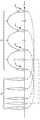
以下に、高調波の影響を回避する帯域の特定手法について説明する。図4は、2次高調波の影響を例示する各データ信号のスペクトル分布図である。図中、例として、低周波数帯域Faに、100(Mbps)の帯域幅を有する4つのチャネル(つまり、データ信号)が、高周波数帯域Fbに、1(Gbps)の帯域幅を有する3つのチャネルが、割り当てられている。低周波数帯域Faの各信号の中心周波数は、4(GHz)、5(GHz)、6(GHz)、及び7(GHz)であり、他方、高周波数帯域Fbの各信号の中心周波数は、8(GHz)、11(GHz)、及び13(GHz)である。 Hereinafter, a method for identifying a band that avoids the influence of harmonics will be described. FIG. 4 is a spectrum distribution diagram of each data signal illustrating the influence of the second harmonic. In the figure, as an example, four channels (that is, data signals) having a bandwidth of 100 (Mbps) in the low frequency band Fa and three channels having a bandwidth of 1 (Gbps) in the high frequency band Fb. Is assigned. The center frequency of each signal in the low frequency band Fa is 4 (GHz), 5 (GHz), 6 (GHz), and 7 (GHz), while the center frequency of each signal in the high frequency band Fb is 8 (GHz), 11 (GHz), and 13 (GHz).
これらの信号を、光FDM技術により多重した場合、低周波数帯域Faの各信号の2次高調波Fhは、2倍の周波数である8(GHz)、10(GHz)、12(GHz)、及び14(GHz)を中心周波数として生ずる(各点線を参照)。このとき、高調波Fhの帯域は、高周波数帯域Fbの各信号のサイドローブと部分的に重なるに過ぎないので、高周波数帯域Fbに対する高調波Fhの影響は、実質的に生じない。 When these signals are multiplexed by the optical FDM technology, the second harmonic Fh of each signal in the low frequency band Fa is twice as high as 8 (GHz), 10 (GHz), 12 (GHz), and 14 (GHz) is generated as a center frequency (see each dotted line). At this time, since the band of the harmonic Fh only partially overlaps the side lobe of each signal in the high frequency band Fb, the influence of the harmonic Fh on the high frequency band Fb does not substantially occur.
一方、図中の点線で示されるように、仮に、4.5(GHz)を中心周波数とする信号を割り当てた場合、該周波数の2倍である9(GHz)を中心周波数とする高調波が生ずる(一点鎖線を参照)。この高調波は、9(GHz)の信号のメインローブと重なるため、当該信号の品質を劣化させてしまう(図中の「NG」参照)。 On the other hand, as shown by the dotted line in the figure, if a signal having a center frequency of 4.5 (GHz) is assigned, a harmonic having a center frequency of 9 (GHz), which is twice that frequency, is generated. Occurs (see dashed line). Since the harmonics overlap with the main lobe of the 9 (GHz) signal, the quality of the signal is degraded (see “NG” in the figure).
上述した原理に基づき、管理装置4の制御部40は、より広い帯域内に、より多くのデータ信号が多重可能となるように、各データ信号Siの多重に用いられる利用周波数帯域を特定する。図5は、利用周波数帯域を示すスペクトル分布図である。図中、Fmaxは、光変調器200に固有の変調可能帯域である。また、Fxは、利用周波数帯域の幅であり、Fcenterは、利用周波数帯域の中心周波数である。なお、本説明は、2次高調波のみを対象とする。 Based on the above-described principle, the
利用周波数帯域の特定手法は、次の2つの点に従う。一方は、データ信号Siに使用される帯域幅の2倍の帯域内には、他のデータ信号の周波数を割り当てることができない点である。例えば、100(MHz)の帯域幅の信号を割り当てた場合、当該信号の中心周波数に対して±100(MHz)の帯域内に他信号の中心周波数を割り当てることは不可能である。他方は、図4を参照して述べたとおり、割り当て済みの信号の中心周波数の2倍の周波数は、当該信号の2次高調波成分と重なるために使用不可能である点である。 The method for identifying the used frequency band follows the following two points. On the other hand, the frequency of another data signal cannot be assigned within a band twice the bandwidth used for the data signal Si. For example, when a signal having a bandwidth of 100 (MHz) is assigned, it is impossible to assign the center frequency of another signal within a band of ± 100 (MHz) with respect to the center frequency of the signal. On the other hand, as described with reference to FIG. 4, a frequency twice the center frequency of the assigned signal cannot be used because it overlaps with the second harmonic component of the signal.
上記の2つの点から次式が得られる。
Fx≦Fmax/2 (式1)
2・(Fcenter−Fx/2)≧2(Fcenter+Fx/2) (式2)From the above two points, the following equation is obtained.
Fx ≦ Fmax / 2 (Formula 1)
2 · (Fcenter−Fx / 2) ≧ 2 (Fcenter + Fx / 2) (Formula 2)
したがって、上記の式1、及び式2に基づき、以下のように理想的なFcenterが算出される。
Fcenter=(3/4)・Fmax (式3)Therefore, based on the
Fcenter = (3/4) · Fmax (Formula 3)
例えば、10(GHz)の変調帯域を有する光変調器200を使用する場合、Fmax=10であるから、式3に従って、Fcenter=7.5(GHz)となる。そして、Fx=3(GHz)の帯域幅内に各信号を割り当てる場合、利用周波数帯域は、7.5±1.5(GHz)、つまり、6〜9(GHz)となる。なお、式3によらず、単に、Fmax/2〜Fmaxを利用周波数帯域としてもよい。このように、管理装置4は、2次高調波の影響を回避する場合、光変調器200の変調帯域Fmaxの中心周波数(つまり、Fmax/2)より高い帯域から、利用周波数帯域を特定する。 For example, when the
また、2次高調波だけではなく、3次以上の高調波成分も考慮した場合、式2と同様に次式が得られる。
N・(Fcenter−Fx/2)≧2(Fcenter+Fx/2) (式4)
ここで、N=2,3,・・・・である。Further, when not only the second-order harmonic but also the third-order or higher-order harmonic component is considered, the following formula is obtained in the same manner as the
N · (Fcenter−Fx / 2) ≧ 2 (Fcenter + Fx / 2) (Formula 4)
Here, N = 2, 3,.
したがって、式4に基づき、以下のように理想的なFcenterが算出される。
Fcenter≧(N+1)/{2・(N−1)}・Fx (式5)Therefore, based on
Fcenter ≧ (N + 1) / {2 · (N−1)} · Fx (Formula 5)
例えば、10(GHz)の変調帯域を有する光変調器200を使用して、Fx=4(GHz)の帯域幅内に各信号を割り当てる場合、2次高調波成分の影響を回避するとき、式5により、6.0±2.0(GHz)、つまり、4〜8(GHz)となる。また、3次高調波成分の影響を回避するとき、4.0±2.0(GHz)、つまり、2〜6(GHz)となり、4次高調波成分の影響を回避するとき、3.33±2.0(GHz)、つまり、1.33〜5.33(GHz)となる。さらに、2次、及び3次高調波成分の両方の影響を回避する場合、上記の4〜8(GHz)、及び2〜6(GHz)に共通する帯域である4〜6(GHz)を利用周波数帯域とする。なお、他の次数の高調波成分に関しても同様の手法により利用周波数帯域が得られる。 For example, when assigning each signal within the bandwidth of Fx = 4 (GHz) using the
管理装置4の制御部40は、上述した手法により特定された利用周波数帯域において、各データ信号Siの周波数fi(中心周波数)の割り当てを管理する。図6は、周波数帯域の割り当てを示す帯域分布図である。図中、帯域B0は、要求信号REQiに割り当てられ、帯域B1〜B3は、データ信号S1〜S3にそれぞれ割り当てられているとする。また、利用周波数帯域(Fx参照)は、2次高調波成分の影響が回避されるように、Fmax/2〜Fmaxに帯域内に設定されているものとする。 The
管理装置4の制御部40は、データ信号S1〜S3が使用する各帯域間に未使用の帯域が生じないように、利用周波数帯域の下限F_lowerから順次に周波数を割り当てる。ここで、下限F_lowerは、既に述べたようにFcenter−Fx/2である。 The
制御部40は、新たに多重するデータ信号Siに使用される帯域の下限が、使用中の帯域B0〜B3の上限と接するように、割り当て済みの全帯域B0〜B3の上限F_upper(t)を算出し、この上限F_upper(t)を基準として割り当てを行う。つまり、制御部40は、利用周波数帯域のうち、割り当て済みの全帯域B0〜B3の上限F_upper(t)、及び、新たに多重するデータ信号が占有する帯域幅BWiに基づいて、該データ信号Siに割り当てる周波数F_add(中心周波数)を決定する。このとき、以下の式が成立する。
F_add=F_upper(t)+BWi+α (式6)
ここで、αは、隣の帯域B3との間に設けられる間隔である。なお、帯域幅BWiは、要求信号REQiに含まれる。The
F_add = F_upper (t) + BWi + α (Formula 6)
Here, α is an interval provided between the adjacent band B3. Note that the bandwidth BWi is included in the request signal REQi.
そして、新たに多重されたデータ信号Siが使用する帯域の上限、つまり、割り当て後のF_upper(t+1)は、以下の式により算出される。
F_upper(t+1)=F_upper(t)+2・(BWi+α) (式7)Then, the upper limit of the band used by the newly multiplexed data signal Si, that is, F_upper (t + 1) after allocation is calculated by the following equation.
F_upper (t + 1) = F_upper (t) + 2 · (BWi + α) (Expression 7)
また、利用周波数帯域の外に帯域を割り当てることは不可能であるから、以下の条件式が成立する。
F_upper(t+1)≦F_limit (式8)
ここで、制限値F_limitは、利用周波数帯域の上限であり、Fcenter+Fx/2である。Further, since it is impossible to allocate a band outside the use frequency band, the following conditional expression is established.
F_upper (t + 1) ≦ F_limit (Formula 8)
Here, the limit value F_limit is the upper limit of the use frequency band and is Fcenter + Fx / 2.
制御部40は、要求信号REQiを受信した場合、式6に基づいて算出した周波数F_addを、割り当てる周波数として応答信号RESに含め、多重送信装置(i)2に送信する。そして、制御部40は、式7に基づいて、新たなF_upper(t+1)を算出する。 When receiving the request signal REQi, the
このように、制御部40は、新たに多重するデータ信号Siに周波数fiを割り当てるために、割り当て済みの帯域の上限F_upper(t)をポインタとして利用し、式6に従って割り当てる周波数F_addを算出する。また、制御部40は、次回の割り当てに備えて、式7に従って新たなF_upper(t+1)を算出する。したがって、管理装置4は、簡便に、効率的な割り当て処理を行うことができる。 In this way, the
また、さらに効率的な割り当て処理を実現するために、管理装置4は、使用されなくなった帯域から周波数の再割り当てを行ってもよい。図7は、未使用状態の周波数帯域を含む帯域分布図である。図には、例として、図6の帯域B1,B3が未使用になった場合が示されている(点線を参照)。 Further, in order to realize more efficient allocation processing, the
多重送信装置(i)2は、データ信号Siの多重を停止する場合、停止を要求する要求信号REQiを送信する。本例の場合、管理装置4に対して、多重送信装置(1),(3)2から帯域割り当ての停止を要求する要求信号REQiが送信され、制御部40は、該要求信号REQiに応じて、帯域B1,B3の割り当てを停止する。このため、利用周波数帯域の中に、間隔をおいて2つの未使用状態の帯域B1,B3が生ずる。制御部40は、未使用状態の帯域B1,B3を、割り当て済みの帯域とともに、管理テーブル410により管理し、新たに多重するデータ信号Siに割り当てる。 When stopping multiplexing of the data signal Si, the multiplex transmitter (i) 2 transmits a request signal REQi for requesting the stop. In the case of this example, a request signal REQi for requesting stop of band allocation is transmitted from the multiple transmission devices (1) and (3) 2 to the
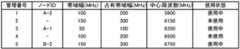
図8には、管理テーブル410の一例が示されている。管理テーブル410には、管理番号、ノードID、帯域幅、占有帯域幅、中心周波数、及び使用状態が、対応付けられて記録されている。 FIG. 8 shows an example of the management table 410. In the management table 410, a management number, a node ID, a bandwidth, an occupied bandwidth, a center frequency, and a usage state are recorded in association with each other.
管理番号は、制御部40が、管理テーブル410内のデータを識別するために付与する番号であり、例えば時系列に付与される。ノードIDは、周波数を割り当てたデータ信号Siを送信する多重送信装置2の識別情報を示す。なお、未使用状態の帯域については、ノードIDは記録されない(「−」を参照)。 The management number is a number assigned by the
帯域幅は、データ信号Siが占有する帯域幅BWi、または未使用状態の帯域幅を示す。占有帯域幅は、帯域幅の2倍の幅を示す。なお、上記の間隔αが設定されている場合、占有帯域幅は、帯域幅の2倍の幅に、2×αが加算された値となる。使用状態は、当該帯域が、使用中、及び未使用の何れであるかを示す。つまり、使用状態は、割り当て済みの帯域について使用中を示し、他方、要求信号REQiにより停止が要求された帯域について未使用を示す使用情報である。 The bandwidth indicates a bandwidth BWi occupied by the data signal Si or an unused bandwidth. The occupied bandwidth indicates twice the bandwidth. When the above-mentioned interval α is set, the occupied bandwidth is a value obtained by adding 2 × α to twice the bandwidth. The use state indicates whether the band is in use or unused. That is, the usage state is usage information indicating that the allocated band is being used, and on the other hand, indicating that the band requested to be stopped by the request signal REQi is not used.
このように、管理装置4は、複数の多重送信装置(1)〜(n)2の各々について、データ信号Siに割り当てられた周波数、帯域幅、及び使用情報が記録された管理テーブル410を有する。そして、管理装置4は、複数の多重送信装置(1)〜(n)2の何れかがデータ信号Siの多重を停止した場合、該多重送信装置(i)に対応する使用情報を、未使用を示す状態に更新する。これにより、管理装置4は、帯域割り当ての管理を簡便に行い、さらに、未使用状態の帯域から周波数の再割り当てを容易に行うことができる。 As described above, the
図9は、管理装置4の割り当て処理の動作を示すフロー図である。制御部40は、多重送信装置(i)2から周波数割り当ての要求信号REQiを受信した場合(ステップSt1のYES)、未使用状態の帯域の有無を確認する(ステップSt2)。この処理において、制御部40は、管理テーブル410を参照し、使用状態が未使用を示す帯域を検索する。一方、要求信号REQiを受信していない場合(ステップSt1のNO)、制御部40は、処理を終了する。 FIG. 9 is a flowchart showing the operation of the assignment process of the
制御部40は、未使用状態の帯域が存在する場合(ステップSt2のYES)、要求信号REQiに含まれる帯域幅BWiに基づいて、2×BWiが当該未使用状態の帯域の占有帯域幅以下であるか否かを判定する(ステップSt3)。この処理において、制御部40は、管理テーブル410を参照し、当該未使用状態の帯域の占有帯域幅を取得して、2×BWiと比較する。 When there is an unused band (YES in step St2), the
比較の結果、2×BWiが当該未使用状態の帯域の占有帯域幅以下である場合(ステップSt3のYES)、制御部40は、当該未使用状態の帯域内の周波数を、対応するデータ信号Siに割り当てる(ステップSt4)。割り当て手法は、図6を参照して述べたものと同様である。つまり、制御部40は、未使用状態の各帯域について、Fi_upper(t)を算出し、Fi_upper(t)に基づき、新たに多重するデータ信号Siに割り当てる周波数Fi_addを決定する(図7参照)。 As a result of the comparison, when 2 × BWi is equal to or smaller than the occupied bandwidth of the unused band (YES in Step St3), the
一方、2×BWiが当該未使用状態の帯域の占有帯域幅以下ではない場合(ステップSt3のNO)、制御部40は、管理テーブル410を参照して、他の未使用状態の帯域を検索し(ステップSt7)、再びステップSt2から処理を行う。 On the other hand, when 2 × BWi is not less than or equal to the occupied bandwidth of the unused band (NO in step St3), the
周波数の割り当て後、制御部40は、管理テーブル410を更新する(ステップSt5)。この処理において、制御部40は、割り当てた周波数fi、及び帯域幅BWiなどを管理テーブル410に登録する。また、制御部40は、未使用状態の帯域に余剰帯域が存在する場合、つまり、当該未使用状態の帯域の占有帯域幅−2×BWi>0である場合、当該余剰帯域を、新たな未使用状態の帯域として、管理テーブル410に登録する。 After the frequency assignment, the
次に、制御部40は、要求信号REQiの送信元の多重送信装置(i)2に、割り当てた周波数fiを通知する(ステップSt6)。この通知は、応答信号RESとして送信される。制御部40は、通知後に処理を終了する。なお、ステップSt5及びステップSt6は、処理順序が互いに逆であってもよい。 Next, the
一方、制御部40は、管理テーブル410内に未使用状態の帯域が存在しない場合(ステップSt2)、F_upper(t+1)≦F_limitが成立するか否かを判定する(ステップSt8)。ここで、F_upper(t+1)は、上記の式7に基づいて算出される。また、F_limitは、上述したように、利用周波数帯域の上限値、つまりFcenter+Fx/2である。 On the other hand, when there is no unused band in the management table 410 (step St2), the
F_upper(t+1)≦F_limitが成立する場合(ステップSt8のYES)、制御部40は、上記の式6に基づいて周波数F_addを算出して、当該データ信号Siに割り当てる(ステップSt9)。割り当てが完了すると、制御部40は、管理テーブル410の更新処理(ステップSt5)、及び割り当てた周波数F_add(fi)の通知処理(ステップSt6)を行う。 When F_upper (t + 1) ≦ F_limit is satisfied (YES in step St8), the
一方、F_upper(t+1)≦F_limitが成立しない場合(ステップSt8のNO)、制御部40は、割り当て可能な周波数が存在しないと判断し、その旨を当該多重送信装置(i)2に、応答信号RESによって通知する(ステップSt10)。制御部40は、通知後に処理を終了する。 On the other hand, if F_upper (t + 1) ≦ F_limit is not satisfied (NO in step St8), the
このように、管理装置4は、管理テーブル410内の使用情報に基づいて、利用周波数帯域内に未使用状態の帯域が存在すると判断した場合、未使用状態の帯域内の周波数fiを、新たに多重するデータ信号Siに割り当てる。したがって、割り当て済みの帯域が未使用状態になった場合において、管理装置4は、当該帯域内の周波数を再割り当てでき、限られた帯域のリソースを、より効率的に利用することが可能である。 As described above, when the
これまで説明した帯域割り当ての手法は、割り当て済みの帯域の上限F_upper(t)を基準としたものであったが、これとは逆に、割り当て済みの帯域の下限を基準としてもよい。この場合、管理装置4は、利用周波数帯域の上限、つまりFcenter+Fx/2から順次に周波数を割り当て、割り当て済みの全帯域の下限をポインタとして算出する。したがって、管理装置4は、利用周波数帯域のうち、割り当て済みの全帯域の下限、及び、新たに多重するデータ信号が占有する帯域幅BWiに基づいて、該データ信号に割り当てる周波数を決定する。このとき、割り当ての制限F_limitは、利用周波数帯域の下限、つまりFcenter−Fx/2となる。この場合においても、上述した内容と同様に、効率的な割り当て処理が行われる。 The band allocation methods described so far have been based on the allocated bandwidth upper limit F_upper (t), but conversely, the allocated bandwidth lower limit may be used as a reference. In this case, the
また、上述した第1実施例において、複数の多重送信装置(1)〜(n)2は、データ信号Siの多重を開始するとき、利用周波数帯域内の所定の周波数f0の要求信号REQiを搬送光νcに多重する。つまり、要求信号REQiは、利用周波数帯域内の周波数大域を用いて送信される。そして、管理装置4は、受信装置3を介して受信した要求信号REQiに応じて、データ信号Siに周波数を割り当てる。したがって、要求信号REQiは、他のデータ信号Siと同様の手法により送受信が可能であるから、他と異なる特別な送信手段、及び受信手段を用いることがなく、簡便で低コストな制御システムが実現される。もっとも、要求信号REQiの送信手段は、これに限定されることはない。 Further, in the first embodiment described above, when the plurality of multiplex transmission devices (1) to (n) 2 start multiplexing the data signal Si, the plurality of multiplex transmission devices (1) to (n) 2 carry the request signal REQi having a predetermined frequency f0 within the use frequency band. Multiplexed to light νc. That is, the request signal REQi is transmitted using the frequency band within the use frequency band. Then, the
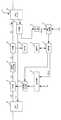
図10は、第2実施例の多重送信装置2の構成図である。図中、第1実施例と同一の構成については、同じ符号を付し、その説明を省略する。第2実施例において、要求信号REQiは、搬送光νcの波長λcとは異なる他の波長λrqの信号として送信される(グラフG5を参照)。 FIG. 10 is a configuration diagram of the
本実施例の多重送信装置2は、変調信号生成部20と、合波器21と、非線形光学媒質22と、分波器23と、終端器24と、制御部25と、記憶部26と、通信処理部27と、合波器50と、要求信号変調部51とを含む。制御部25は、要求信号REQiを、波長λrqの光源と光変調器とを含む要求信号変調部1に出力して、波長λrqの光信号に変調する。この光信号は、WDMカプラなどの合波器50を介して伝送路に入力される。 The
一方、図11は、第2実施例の受信ノードNの構成図である。図中、第1実施例と同一の構成については、同じ符号を付し、その説明を省略する。 On the other hand, FIG. 11 is a block diagram of the receiving node N of the second embodiment. In the figure, the same components as those of the first embodiment are denoted by the same reference numerals, and the description thereof is omitted.
本実施例の受信装置3は、分波器35と、PD30,36と、分波器31と、複数組のチューナブル・バンドパスフィルタ32、増幅器33、及び復調回路34とを有する。分波器35は、伝送路から入力された搬送光λc(νc)、及び、要求信号REQiを変調して得た光信号λrqを、PD30,36にそれぞれ分波する。PD36は、波長λrqの光信号を光電変換することにより要求信号REQiを得て、制御部40に出力する。 The receiving
本実施例において、複数の多重送信装置(1)〜(n)2は、データ信号Siの多重を開始するとき、搬送光νcとは異なる波長光の要求信号REQiを、伝送路を介して受信装置3に送信する。そして、管理装置4は、受信装置3を介して受信した要求信号REQiに応じて、データ信号Siに周波数fiを割り当てる。したがって、搬送光νc、及び要求信号REQiが、互いに独立して処理されるため、仮に、搬送光源10が故障した場合であっても、要求信号REQiの送信は可能であり、通信の信頼性が向上する。 In the present embodiment, when a plurality of multiplex transmission apparatuses (1) to (n) 2 start multiplexing of the data signal Si, they receive a request signal REQi of light having a wavelength different from that of the carrier light νc via the transmission line. Transmit to
また、上述した第1及び第2実施例において、管理装置4は、搬送光νcの伝送路とは異なる他の通信ネットワークNWを介して、応答信号RESを各多重送信装置(i)2に送信するが、これに限定されない。図12は、第3実施例に係る光伝送システム1の構成図である。本実施例において、応答信号RESは、搬送光νcと同一の伝送路を介し、搬送光νcの波長λcとは異なる他の波長λrsの信号として送信される(グラフG6を参照)。 In the first and second embodiments described above, the
図13は、第3実施例の受信ノードNの構成図である。図中、第1実施例と同一の構成については、同じ符号を付し、その説明を省略する。 FIG. 13 is a configuration diagram of the receiving node N of the third embodiment. In the figure, the same components as those of the first embodiment are denoted by the same reference numerals, and the description thereof is omitted.
本実施例の受信装置3は、WDMフィルタ38と、PD30と、分波器31と、複数組のチューナブル・バンドパスフィルタ32、増幅器33、及び復調回路34と、光変調器37とを有する。光変調器37は、例えばLDであり、制御部4から入力された応答信号RESを、波長λrsの光信号に変調してWDMフィルタ38に出力する。なお、光変調器37として、LN変調器を採用し、外部変調により応答信号RESの変調処理を行ってもよい。 The receiving
WDMフィルタ38は、異なる波長の2つの光が、互いに反対方向に伝送される伝送路を、波長ごとの伝送路に分岐するデバイスである。WDMフィルタ38は、伝送路から入力された搬送光λc(νc)をPD30に導き、他方、光変調器37から入力された波長λrsの光信号を、該伝送路へと導く。 The
図14は、第3実施例の多重送信装置2の構成図である。図中、第1実施例と同一の構成については、同じ符号を付し、その説明を省略する。 FIG. 14 is a configuration diagram of the
多重送信装置2は、変調信号生成部20と、合波器21と、非線形光学媒質22と、分波器23,42と、終端器24と、制御部25と、記憶部26と、通信処理部27と、選択回路28と、WDMフィルタ44,45と、PD43とを含む。WDMフィルタ44,45は、上記のWDMフィルタ38と同様である。 The
WDMフィルタ44は、受信装置3から伝送路を介して入力された波長λrsの光信号を、分波器42に導き、他方、分波器23から入力された搬送光λc(νc)を該伝送路に導く。分波器42は、例えば光カプラであり、波長λrsの光信号を分波して、WDMフィルタ45、及びPD43に導く。PD43は、波長λrsの光信号を光電変換し、これにより得た応答信号RESを通信処理部27に出力する。 The
WDMフィルタ45は、搬送光λc(νc)を該伝送路に導くとともに、隣の多重送信装置(i−1)2が受信するように、波長λrsの光信号を伝送路に導く。このため、応答信号RESは、受信装置3と伝送路を介して接続された全ての多重送信装置(1)〜(n)2において受信される。応答信号RESは、宛先の多重送信装置(1)〜(n)2を識別する宛先情報を含むため、多重送信装置(1)〜(n)2は、宛先情報を参照して、自装置宛ての応答信号RESのみを処理する。なお、本実施例において、WDMフィルタ44,45に代えて、光サーキュレータなどの光方向性結合器を有する他のデバイスを用いてもよい。 The
このように、本実施例において、管理装置4は、データ信号Siに周波数fiを割り当てるとき、搬送光λc(νc)とは異なる波長光λrsの制御信号RESを、搬送光λc(νc)と共通の伝送路を介して、複数の多重送信装置(1)〜(n)2に送信する。したがって、本実施例の管理装置4は、第1及び第2実施例とは異なり、他の通信ネットワークNWを用いることなく、単一の伝送路を用いて、要求信号REQi、及び応答信号RESを送受信するため、低コストな制御系が実現される。 Thus, in this embodiment, when the
また、これまで述べた実施例において、管理装置4は、要求信号REQiに含まれる帯域幅BWiに基づいて、割り当てる周波数fiを決定するが、これに限定されない。例えば、管理テーブル410が、管理装置4、及び多重送信装置(i)2の間において共有され、多重送信装置(i)2は、管理テーブル410に基づいて周波数fiを決定し、要求信号REQiに含めて管理装置4に送信してもよい。この場合、管理装置4は、例えば、一定周期、または管理テーブル410の更新時に、管理テーブル410を各多重送信装置(i)2に送信し、多重送信装置2は、受信した管理テーブル410を記憶部26に記憶するとよい。 In the embodiment described so far, the
また、受信装置3は、チューナブル・バンドパスフィルタ32を用いて、各データ信号Siを取り出すようにしたが、これに限定されない。例えば、受信装置3は、通過する周波数、及び帯域が互いに異なる複数のバンドパスフィルタを備え、複数のバンドパスフィルタのうち、割り当てた周波数、及び帯域に該当するフィルタを個別に選択してデータ信号Siを取り出してもよい。 Further, although the receiving
以上、好ましい実施例を参照して本発明の内容を具体的に説明したが、本発明の基本的技術思想及び教示に基づいて、当業者であれば、種々の変形態様を採り得ることは自明である。 Although the contents of the present invention have been specifically described above with reference to the preferred embodiments, it is obvious that those skilled in the art can take various modifications based on the basic technical idea and teachings of the present invention. It is.
1 光伝送システム
2 多重送信装置
200 光変調器
3 受信装置
4 管理装置
410 管理テーブル
νc 搬送光
Si データ信号
fi 周波数
REQi 要求信号
RES 応答信号DESCRIPTION OF
Claims (10)
Translated fromJapanese前記伝送路から入力された前記搬送光を光電変換することにより、前記複数の多重送信装置により多重された前記データ信号の各々を受信する受信装置と、
前記複数の多重送信装置のうち、1つの多重送信装置の前記データ信号に使用される帯域幅の2倍の帯域内には、他の多重送信装置の前記データ信号の前記周波数が割り当てられず、前記データ信号に割り当て済みの前記周波数の2倍の周波数が使用されないように、前記複数の多重送信装置の各々の前記光変調器に共通する変調帯域に基づいて利用周波数帯域を特定し、前記利用周波数帯域において、前記データ信号の前記周波数の割り当てを管理する管理装置とを有することを特徴とする光伝送システム。A plurality of multiplex transmissions that multiplex the data signals to the carrier light by modulating data signals of different frequencies by optical modulators and inputting the signals to a plurality of nonlinear optical media provided in the transmission path of the carrier light, respectively. Equipment,
A receiver that receives each of the data signals multiplexed by the plurality of multiplex transmitters by photoelectrically converting the carrier light input from the transmission path;
Of the multiple multiplex transmitters, the frequency of the data signal of another multiplex transmitter is not allocated in a band twice the bandwidth used for the data signal of one multiplex transmitter, A use frequency band is specified based ona modulation bandcommon to the optical modulatorsof each of the plurality of multiplex transmission devices so that a frequency twice the frequency allocated to the data signal is not used. An optical transmission system comprising: a management device that manages allocation of the frequency of the data signal in a frequency band.
前記管理装置は、前記受信装置を介して受信した前記要求信号に応じて、前記データ信号に周波数を割り当てることを特徴とする請求項1乃至5の何れかに記載の伝送システム。The plurality of multiplex transmission devices, when starting multiplexing of the data signal, multiplex a request signal of a predetermined frequency within the use frequency band to the carrier light,
The transmission system according to claim 1, wherein the management device assigns a frequency to the data signal in accordance with the request signal received via the receiving device.
前記管理装置は、前記受信装置を介して受信した前記要求信号に応じて、前記データ信号に周波数を割り当てることを特徴とする請求項1乃至5の何れかに記載の伝送システム。When the plurality of multiplex transmission devices start multiplexing the data signal, the request signal having a wavelength light different from the carrier light is transmitted to the reception device via the transmission path,
The transmission system according to claim 1, wherein the management device assigns a frequency to the data signal in accordance with the request signal received via the receiving device.
前記伝送路から入力された前記搬送光を光電変換することにより、前記複数の多重送信装置により多重された前記データ信号の各々を受信する受信装置と、
前記複数の多重送信装置の各々の前記光変調器に共通する変調帯域に基づいて利用周波数帯域を特定し、前記利用周波数帯域において、前記データ信号の前記周波数の割り当てを管理する管理装置とを有し、
前記管理装置は、Fxを前記利用周波数帯域の幅とし、Fcenterを前記利用周波数帯域の中心周波数とし、Nを2以上の整数としたとき、以下の式(1)及び(2)の条件
(1)N・(Fcenter−Fx/2)≧2(Fcenter+Fx/2)
(2)Fcenter≧(N+1)/{2・(N−1)}・Fx
が満たされるように、前記利用周波数帯域を特定することを特徴とする光伝送システム。A plurality of multiplex transmissions that multiplex the data signals to the carrier light by modulating data signals of different frequencies by optical modulators and inputting the signals to a plurality of nonlinear optical media provided in the transmission path of the carrier light, respectively. Equipment,
A receiver that receives each of the data signals multiplexed by the plurality of multiplex transmitters by photoelectrically converting the carrier light input from the transmission path;
A management device that identifies a use frequency band based ona modulation bandcommon toeach of the optical modulatorsof each of the plurality of multiplex transmission devices, and manages allocation of the frequency of the data signal in the use frequency band.And
When the management device has Fx as the width of the usage frequency band, Fcenter as the center frequency of the usage frequency band, and N as an integer of 2 or more, the conditions of the following expressions (1) and (2)
(1) N · (Fcenter−Fx / 2) ≧ 2 (Fcenter + Fx / 2)
(2) Fcenter ≧ (N + 1) / {2 · (N−1)} · Fx
The optical transmission system is characterizedin that theuse frequency band is specified so that
Priority Applications (3)
| Application Number | Priority Date | Filing Date | Title |
|---|---|---|---|
| JP2012087975AJP5924088B2 (en) | 2012-04-06 | 2012-04-06 | Optical transmission system |
| GB1302486.4AGB2501159A (en) | 2012-04-06 | 2013-02-13 | Managing frequency allocation in sub-carrier multiplex/multiple access system to avoid harmonic interference |
| US13/767,077US9077470B2 (en) | 2012-04-06 | 2013-02-14 | Optical transmission system using cross phase modulation |
Applications Claiming Priority (1)
| Application Number | Priority Date | Filing Date | Title |
|---|---|---|---|
| JP2012087975AJP5924088B2 (en) | 2012-04-06 | 2012-04-06 | Optical transmission system |
Publications (2)
| Publication Number | Publication Date |
|---|---|
| JP2013219529A JP2013219529A (en) | 2013-10-24 |
| JP5924088B2true JP5924088B2 (en) | 2016-05-25 |
Family
ID=47999019
Family Applications (1)
| Application Number | Title | Priority Date | Filing Date |
|---|---|---|---|
| JP2012087975AExpired - Fee RelatedJP5924088B2 (en) | 2012-04-06 | 2012-04-06 | Optical transmission system |
Country Status (3)
| Country | Link |
|---|---|
| US (1) | US9077470B2 (en) |
| JP (1) | JP5924088B2 (en) |
| GB (1) | GB2501159A (en) |
Families Citing this family (5)
| Publication number | Priority date | Publication date | Assignee | Title |
|---|---|---|---|---|
| CN102439994B (en)* | 2011-07-22 | 2013-11-06 | 华为技术有限公司 | Method and device for adjusting optical device filtering bandwidth |
| JP5924088B2 (en)* | 2012-04-06 | 2016-05-25 | 富士通株式会社 | Optical transmission system |
| US20170273085A1 (en)* | 2014-08-25 | 2017-09-21 | Telefonaktiebolaget Lm Ericsson (Publ) | Subcarrier allocation device and method for allocating n channels to carrier frequencies |
| CN108702208B (en)* | 2016-02-19 | 2020-07-24 | 华为技术有限公司 | Optical channel monitoring using spread spectrum pilot tones |
| CN111698187A (en)* | 2019-12-13 | 2020-09-22 | 广东工业大学 | Frequency division multiple access communication method based on harmonic modulation technology |
Family Cites Families (25)
| Publication number | Priority date | Publication date | Assignee | Title |
|---|---|---|---|---|
| JPS6290045A (en)* | 1985-10-16 | 1987-04-24 | Kokusai Denshin Denwa Co Ltd <Kdd> | Frequency allocation method in FDMA communication system |
| US4953156A (en)* | 1988-09-08 | 1990-08-28 | Gte Laboratories, Incorporated | Wideband subcarrier multiplexed optical communication system operating over more than one octave |
| US5134509A (en)* | 1988-12-22 | 1992-07-28 | Gte Laboratories Incorporated | Coherent subcarrier multiplexed optical communication system |
| DE3902746A1 (en)* | 1989-01-31 | 1990-08-09 | Standard Elektrik Lorenz Ag | OPTICAL BROADBAND MESSAGE TRANSMISSION SYSTEM, ESPECIALLY FOR THE SUBSCRIBER CONNECTION AREA |
| EP0772314A3 (en)* | 1990-09-14 | 1997-09-03 | Fujitsu Ltd | Optical communication system with sub-carrier multiplexing |
| JPH0818514A (en)* | 1994-06-29 | 1996-01-19 | Fujitsu Ltd | Optical subscriber system Same wavelength bidirectional transmission system |
| US5956642A (en)* | 1996-11-25 | 1999-09-21 | Telefonaktiebolaget L M Ericsson | Adaptive channel allocation method and apparatus for multi-slot, multi-carrier communication system |
| JP3295029B2 (en)* | 1996-11-29 | 2002-06-24 | 松下電器産業株式会社 | Optical transmission device and system |
| WO2002061981A2 (en)* | 2001-01-30 | 2002-08-08 | Kestrel Solutions, Inc. | Fiber optic communications |
| KR100584455B1 (en)* | 2005-04-01 | 2006-05-26 | 삼성전자주식회사 | Subcarrier Passive Optical Subscriber Network Using Wavelength Division Multiplexing |
| JP4704842B2 (en)* | 2005-08-01 | 2011-06-22 | 株式会社日立製作所 | WDM type PON system |
| US20080243518A1 (en)* | 2006-11-16 | 2008-10-02 | Alexey Oraevsky | System And Method For Compressing And Reconstructing Audio Files |
| JP4768661B2 (en)* | 2007-04-09 | 2011-09-07 | 日本電信電話株式会社 | Wavelength selection method, apparatus and program in wavelength group network |
| JP4839266B2 (en)* | 2007-06-07 | 2011-12-21 | 株式会社日立製作所 | Optical communication system |
| JP4894659B2 (en)* | 2007-07-19 | 2012-03-14 | Kddi株式会社 | Optical transmission system |
| JP2009225331A (en)* | 2008-03-18 | 2009-10-01 | Toshiba Corp | Device and method for radio communication |
| WO2010146658A1 (en)* | 2009-06-16 | 2010-12-23 | 株式会社日立製作所 | Optical multiplexing terminal device, wavelength multiplexing passive optical network system, and downstream wavelength transmission method |
| US8950933B2 (en)* | 2009-10-15 | 2015-02-10 | Samsung Electronics Co., Ltd. | Apparatus and method for channel aggregation and guard channel indication for visible light communication |
| JP5830872B2 (en)* | 2010-03-19 | 2015-12-09 | 富士通株式会社 | Optical signal processing apparatus, optical communication method, receiver, and optical network system |
| JP5669613B2 (en)* | 2011-02-18 | 2015-02-12 | 沖電気工業株式会社 | Dynamic bandwidth allocation method, optical communication network, and station side apparatus |
| US8805285B2 (en)* | 2011-10-17 | 2014-08-12 | Apple Inc. | System and methods for avoiding interference between communications in different frequency bands |
| JP5924088B2 (en)* | 2012-04-06 | 2016-05-25 | 富士通株式会社 | Optical transmission system |
| JP5935470B2 (en)* | 2012-04-13 | 2016-06-15 | 富士通株式会社 | Optical signal multiplex distribution device, optical communication system, and optical signal multiplex distribution method |
| JP2014049987A (en)* | 2012-08-31 | 2014-03-17 | Fujitsu Ltd | Optical signal receiver, optical signal reception method, and optical frequency division multiplex transmission system |
| JP2014106492A (en)* | 2012-11-29 | 2014-06-09 | Fujitsu Ltd | Apparatus and method for processing optical signal |
- 2012
- 2012-04-06JPJP2012087975Apatent/JP5924088B2/ennot_activeExpired - Fee Related
- 2013
- 2013-02-13GBGB1302486.4Apatent/GB2501159A/ennot_activeWithdrawn
- 2013-02-14USUS13/767,077patent/US9077470B2/ennot_activeExpired - Fee Related
Also Published As
| Publication number | Publication date |
|---|---|
| US20130266320A1 (en) | 2013-10-10 |
| GB201302486D0 (en) | 2013-03-27 |
| JP2013219529A (en) | 2013-10-24 |
| US9077470B2 (en) | 2015-07-07 |
| GB2501159A (en) | 2013-10-16 |
Similar Documents
| Publication | Publication Date | Title |
|---|---|---|
| US11871164B2 (en) | Systems and methods for intelligent edge to edge optical system and wavelength provisioning | |
| US11876560B2 (en) | System and methods for distribution of heterogeneous wavelength multiplexed signals over optical access network | |
| JP6123337B2 (en) | Optical signal processing device, transmission device, and optical signal processing method | |
| US7539419B2 (en) | Optical transmission system for radio access and high frequency optical transmitter | |
| CN102790653B (en) | Reconfigurable optical add-drop multiplexer and reconfigurable optical add-drop multiplexing method | |
| JP5924088B2 (en) | Optical transmission system | |
| US20140099114A1 (en) | Optical signal transmitting apparatus, optical frequency division multiplex transmission system, and optical signal communication method | |
| EP3571791B1 (en) | Systems and methods for intelligent edge to edge optical system and wavelength provisioning | |
| JP5288434B2 (en) | Information distribution system | |
| EP2958253A1 (en) | Optical device comprising mode-locked laser components | |
| Guan et al. | Enabling 5G services in PON with a novel smart edge based on SiP MRM | |
| JP4230888B2 (en) | Frequency converter, frequency conversion method, and optical wireless device using the same | |
| Ware et al. | Quantum-Aware Network Planning and Integration | |
| Yan et al. | Hardware-programmable optical networks | |
| EP2897311A1 (en) | Optical Communication Signal Conversion |
Legal Events
| Date | Code | Title | Description |
|---|---|---|---|
| A621 | Written request for application examination | Free format text:JAPANESE INTERMEDIATE CODE: A621 Effective date:20150203 | |
| A977 | Report on retrieval | Free format text:JAPANESE INTERMEDIATE CODE: A971007 Effective date:20160113 | |
| A131 | Notification of reasons for refusal | Free format text:JAPANESE INTERMEDIATE CODE: A131 Effective date:20160119 | |
| A521 | Request for written amendment filed | Free format text:JAPANESE INTERMEDIATE CODE: A523 Effective date:20160302 | |
| TRDD | Decision of grant or rejection written | ||
| A01 | Written decision to grant a patent or to grant a registration (utility model) | Free format text:JAPANESE INTERMEDIATE CODE: A01 Effective date:20160322 | |
| A61 | First payment of annual fees (during grant procedure) | Free format text:JAPANESE INTERMEDIATE CODE: A61 Effective date:20160404 | |
| R150 | Certificate of patent or registration of utility model | Ref document number:5924088 Country of ref document:JP Free format text:JAPANESE INTERMEDIATE CODE: R150 | |
| LAPS | Cancellation because of no payment of annual fees |