JP5917027B2 - Method for producing electrode material - Google Patents
Method for producing electrode materialDownload PDFInfo
- Publication number
- JP5917027B2 JP5917027B2JP2011139983AJP2011139983AJP5917027B2JP 5917027 B2JP5917027 B2JP 5917027B2JP 2011139983 AJP2011139983 AJP 2011139983AJP 2011139983 AJP2011139983 AJP 2011139983AJP 5917027 B2JP5917027 B2JP 5917027B2
- Authority
- JP
- Japan
- Prior art keywords
- negative electrode
- heat treatment
- storage device
- power storage
- silicon layer
- Prior art date
- Legal status (The legal status is an assumption and is not a legal conclusion. Google has not performed a legal analysis and makes no representation as to the accuracy of the status listed.)
- Expired - Fee Related
Links
- 239000007772electrode materialSubstances0.000titleclaimsdescription41
- 238000004519manufacturing processMethods0.000titleclaimsdescription32
- 238000010438heat treatmentMethods0.000claimsdescription65
- 239000000463materialSubstances0.000claimsdescription51
- PXHVJJICTQNCMI-UHFFFAOYSA-NNickelChemical compound[Ni]PXHVJJICTQNCMI-UHFFFAOYSA-N0.000claimsdescription37
- 150000001875compoundsChemical class0.000claimsdescription29
- 230000004907fluxEffects0.000claimsdescription26
- 229910052759nickelInorganic materials0.000claimsdescription17
- 239000012298atmosphereSubstances0.000claimsdescription11
- 239000011261inert gasSubstances0.000claimsdescription11
- XEEYBQQBJWHFJM-UHFFFAOYSA-NIronChemical compound[Fe]XEEYBQQBJWHFJM-UHFFFAOYSA-N0.000claimsdescription10
- IJGRMHOSHXDMSA-UHFFFAOYSA-NAtomic nitrogenChemical compoundN#NIJGRMHOSHXDMSA-UHFFFAOYSA-N0.000claimsdescription8
- TWRXJAOTZQYOKJ-UHFFFAOYSA-LMagnesium chlorideChemical compound[Mg+2].[Cl-].[Cl-]TWRXJAOTZQYOKJ-UHFFFAOYSA-L0.000claimsdescription8
- FAPWRFPIFSIZLT-UHFFFAOYSA-MSodium chlorideChemical compound[Na+].[Cl-]FAPWRFPIFSIZLT-UHFFFAOYSA-M0.000claimsdescription8
- FGDZQCVHDSGLHJ-UHFFFAOYSA-Mrubidium chlorideChemical compound[Cl-].[Rb+]FGDZQCVHDSGLHJ-UHFFFAOYSA-M0.000claimsdescription8
- WCUXLLCKKVVCTQ-UHFFFAOYSA-MPotassium chlorideChemical compound[Cl-].[K+]WCUXLLCKKVVCTQ-UHFFFAOYSA-M0.000claimsdescription7
- KWGKDLIKAYFUFQ-UHFFFAOYSA-Mlithium chlorideChemical compound[Li+].[Cl-]KWGKDLIKAYFUFQ-UHFFFAOYSA-M0.000claimsdescription7
- XKRFYHLGVUSROY-UHFFFAOYSA-NArgonChemical compound[Ar]XKRFYHLGVUSROY-UHFFFAOYSA-N0.000claimsdescription6
- 229910017052cobaltInorganic materials0.000claimsdescription6
- 239000010941cobaltSubstances0.000claimsdescription6
- GUTLYIVDDKVIGB-UHFFFAOYSA-Ncobalt atomChemical compound[Co]GUTLYIVDDKVIGB-UHFFFAOYSA-N0.000claimsdescription6
- 239000007789gasSubstances0.000claimsdescription5
- UXVMQQNJUSDDNG-UHFFFAOYSA-LCalcium chlorideChemical compound[Cl-].[Cl-].[Ca+2]UXVMQQNJUSDDNG-UHFFFAOYSA-L0.000claimsdescription4
- 239000001110calcium chlorideSubstances0.000claimsdescription4
- 229910001628calcium chlorideInorganic materials0.000claimsdescription4
- 229910052742ironInorganic materials0.000claimsdescription4
- 229910001629magnesium chlorideInorganic materials0.000claimsdescription4
- WPBNNNQJVZRUHP-UHFFFAOYSA-Lmanganese(2+);methyl n-[[2-(methoxycarbonylcarbamothioylamino)phenyl]carbamothioyl]carbamate;n-[2-(sulfidocarbothioylamino)ethyl]carbamodithioateChemical compound[Mn+2].[S-]C(=S)NCCNC([S-])=S.COC(=O)NC(=S)NC1=CC=CC=C1NC(=S)NC(=O)OCWPBNNNQJVZRUHP-UHFFFAOYSA-L0.000claimsdescription4
- 229910052757nitrogenInorganic materials0.000claimsdescription4
- 229940102127rubidium chlorideDrugs0.000claimsdescription4
- 239000011780sodium chlorideSubstances0.000claimsdescription4
- 229910015868MSiOInorganic materials0.000claimsdescription3
- 229910052786argonInorganic materials0.000claimsdescription3
- 239000001307heliumSubstances0.000claimsdescription3
- 229910052734heliumInorganic materials0.000claimsdescription3
- SWQJXJOGLNCZEY-UHFFFAOYSA-Nhelium atomChemical compound[He]SWQJXJOGLNCZEY-UHFFFAOYSA-N0.000claimsdescription3
- 229910052754neonInorganic materials0.000claimsdescription3
- GKAOGPIIYCISHV-UHFFFAOYSA-Nneon atomChemical compound[Ne]GKAOGPIIYCISHV-UHFFFAOYSA-N0.000claimsdescription3
- 239000001103potassium chlorideSubstances0.000claimsdescription3
- 235000011164potassium chlorideNutrition0.000claimsdescription3
- 229910052724xenonInorganic materials0.000claimsdescription3
- FHNFHKCVQCLJFQ-UHFFFAOYSA-Nxenon atomChemical compound[Xe]FHNFHKCVQCLJFQ-UHFFFAOYSA-N0.000claimsdescription3
- 238000003860storageMethods0.000description78
- 229910021417amorphous siliconInorganic materials0.000description53
- 238000000034methodMethods0.000description37
- 239000007773negative electrode materialSubstances0.000description36
- HBBGRARXTFLTSG-UHFFFAOYSA-NLithium ionChemical compound[Li+]HBBGRARXTFLTSG-UHFFFAOYSA-N0.000description33
- 229910001416lithium ionInorganic materials0.000description33
- 229910021419crystalline siliconInorganic materials0.000description23
- 239000002245particleSubstances0.000description18
- 230000003197catalytic effectEffects0.000description17
- 239000003054catalystSubstances0.000description16
- 239000003792electrolyteSubstances0.000description14
- 229910052744lithiumInorganic materials0.000description14
- WHXSMMKQMYFTQS-UHFFFAOYSA-NLithiumChemical compound[Li]WHXSMMKQMYFTQS-UHFFFAOYSA-N0.000description13
- 238000002425crystallisationMethods0.000description13
- 230000008025crystallizationEffects0.000description13
- 230000008569processEffects0.000description12
- 230000006872improvementEffects0.000description11
- 239000008188pelletSubstances0.000description11
- 239000011149active materialSubstances0.000description9
- 238000007599dischargingMethods0.000description9
- 239000007774positive electrode materialSubstances0.000description9
- 239000002904solventSubstances0.000description9
- RTAQQCXQSZGOHL-UHFFFAOYSA-NTitaniumChemical compound[Ti]RTAQQCXQSZGOHL-UHFFFAOYSA-N0.000description8
- 239000013078crystalSubstances0.000description8
- 239000000203mixtureSubstances0.000description8
- 229910052719titaniumInorganic materials0.000description8
- 239000010936titaniumSubstances0.000description8
- 239000010949copperSubstances0.000description7
- CSCPPACGZOOCGX-UHFFFAOYSA-NAcetoneChemical compoundCC(C)=OCSCPPACGZOOCGX-UHFFFAOYSA-N0.000description6
- RYGMFSIKBFXOCR-UHFFFAOYSA-NCopperChemical compound[Cu]RYGMFSIKBFXOCR-UHFFFAOYSA-N0.000description6
- UQSXHKLRYXJYBZ-UHFFFAOYSA-NIron oxideChemical compound[Fe]=OUQSXHKLRYXJYBZ-UHFFFAOYSA-N0.000description6
- 229910052802copperInorganic materials0.000description6
- WMFOQBRAJBCJND-UHFFFAOYSA-MLithium hydroxideChemical compound[Li+].[OH-]WMFOQBRAJBCJND-UHFFFAOYSA-M0.000description5
- 239000004020conductorSubstances0.000description5
- 238000010304firingMethods0.000description5
- 229910052751metalInorganic materials0.000description5
- 230000002194synthesizing effectEffects0.000description5
- LFQSCWFLJHTTHZ-UHFFFAOYSA-NEthanolChemical compoundCCOLFQSCWFLJHTTHZ-UHFFFAOYSA-N0.000description4
- BQCADISMDOOEFD-UHFFFAOYSA-NSilverChemical compound[Ag]BQCADISMDOOEFD-UHFFFAOYSA-N0.000description4
- ATJFFYVFTNAWJD-UHFFFAOYSA-NTinChemical compound[Sn]ATJFFYVFTNAWJD-UHFFFAOYSA-N0.000description4
- 229910045601alloyInorganic materials0.000description4
- 239000000956alloySubstances0.000description4
- 239000003575carbonaceous materialSubstances0.000description4
- AMWRITDGCCNYAT-UHFFFAOYSA-Lhydroxy(oxo)manganese;manganeseChemical compound[Mn].O[Mn]=O.O[Mn]=OAMWRITDGCCNYAT-UHFFFAOYSA-L0.000description4
- 229910052738indiumInorganic materials0.000description4
- APFVFJFRJDLVQX-UHFFFAOYSA-Nindium atomChemical compound[In]APFVFJFRJDLVQX-UHFFFAOYSA-N0.000description4
- 238000003780insertionMethods0.000description4
- 230000037431insertionEffects0.000description4
- 239000011572manganeseSubstances0.000description4
- 239000002184metalSubstances0.000description4
- -1phosphoric acid compoundChemical class0.000description4
- BASFCYQUMIYNBI-UHFFFAOYSA-NplatinumChemical compound[Pt]BASFCYQUMIYNBI-UHFFFAOYSA-N0.000description4
- 239000002210silicon-based materialSubstances0.000description4
- 229910052709silverInorganic materials0.000description4
- 239000004332silverSubstances0.000description4
- 229910052718tinInorganic materials0.000description4
- XLYOFNOQVPJJNP-UHFFFAOYSA-NwaterSubstancesOXLYOFNOQVPJJNP-UHFFFAOYSA-N0.000description4
- OKKJLVBELUTLKV-UHFFFAOYSA-NMethanolChemical compoundOCOKKJLVBELUTLKV-UHFFFAOYSA-N0.000description3
- VYPSYNLAJGMNEJ-UHFFFAOYSA-NSilicium dioxideChemical compoundO=[Si]=OVYPSYNLAJGMNEJ-UHFFFAOYSA-N0.000description3
- XUIMIQQOPSSXEZ-UHFFFAOYSA-NSiliconChemical compound[Si]XUIMIQQOPSSXEZ-UHFFFAOYSA-N0.000description3
- 238000013461designMethods0.000description3
- 238000003795desorptionMethods0.000description3
- NPLZZSLZTJVZSX-UHFFFAOYSA-Liron(2+);oxalate;dihydrateChemical compoundO.O.[Fe+2].[O-]C(=O)C([O-])=ONPLZZSLZTJVZSX-UHFFFAOYSA-L0.000description3
- 239000007788liquidSubstances0.000description3
- XGZVUEUWXADBQD-UHFFFAOYSA-Llithium carbonateChemical compound[Li+].[Li+].[O-]C([O-])=OXGZVUEUWXADBQD-UHFFFAOYSA-L0.000description3
- 238000002156mixingMethods0.000description3
- 229910000480nickel oxideInorganic materials0.000description3
- RUFLMLWJRZAWLJ-UHFFFAOYSA-Nnickel silicideChemical compound[Ni]=[Si]=[Ni]RUFLMLWJRZAWLJ-UHFFFAOYSA-N0.000description3
- 229910021334nickel silicideInorganic materials0.000description3
- 239000000376reactantSubstances0.000description3
- 230000009467reductionEffects0.000description3
- 150000003839saltsChemical class0.000description3
- 229910052710siliconInorganic materials0.000description3
- 239000010703siliconSubstances0.000description3
- 229910052814silicon oxideInorganic materials0.000description3
- OKTJSMMVPCPJKN-UHFFFAOYSA-NCarbonChemical compound[C]OKTJSMMVPCPJKN-UHFFFAOYSA-N0.000description2
- 229910018119Li 3 PO 4Inorganic materials0.000description2
- 229910010707LiFePO 4Inorganic materials0.000description2
- PWHULOQIROXLJO-UHFFFAOYSA-NManganeseChemical compound[Mn]PWHULOQIROXLJO-UHFFFAOYSA-N0.000description2
- 229920002978VinylonPolymers0.000description2
- 230000001133accelerationEffects0.000description2
- MQRWBMAEBQOWAF-UHFFFAOYSA-Nacetic acid;nickelChemical compound[Ni].CC(O)=O.CC(O)=OMQRWBMAEBQOWAF-UHFFFAOYSA-N0.000description2
- 229910000147aluminium phosphateInorganic materials0.000description2
- 238000009792diffusion processMethods0.000description2
- 238000001035dryingMethods0.000description2
- 238000005516engineering processMethods0.000description2
- 229910002804graphiteInorganic materials0.000description2
- 239000010439graphiteSubstances0.000description2
- 229910052808lithium carbonateInorganic materials0.000description2
- GELKBWJHTRAYNV-UHFFFAOYSA-Klithium iron phosphateChemical compound[Li+].[Fe+2].[O-]P([O-])([O-])=OGELKBWJHTRAYNV-UHFFFAOYSA-K0.000description2
- 229910052748manganeseInorganic materials0.000description2
- 239000007769metal materialSubstances0.000description2
- 229940078494nickel acetateDrugs0.000description2
- GNRSAWUEBMWBQH-UHFFFAOYSA-NoxonickelChemical compound[Ni]=OGNRSAWUEBMWBQH-UHFFFAOYSA-N0.000description2
- NBIIXXVUZAFLBC-UHFFFAOYSA-Nphosphoric acidSubstancesOP(O)(O)=ONBIIXXVUZAFLBC-UHFFFAOYSA-N0.000description2
- 229910052697platinumInorganic materials0.000description2
- 230000027756respiratory electron transport chainEffects0.000description2
- 238000004904shorteningMethods0.000description2
- NDVLTYZPCACLMA-UHFFFAOYSA-Nsilver oxideChemical compound[O-2].[Ag+].[Ag+]NDVLTYZPCACLMA-UHFFFAOYSA-N0.000description2
- 239000007787solidSubstances0.000description2
- 238000004544sputter depositionMethods0.000description2
- 229910052723transition metalInorganic materials0.000description2
- 150000003624transition metalsChemical class0.000description2
- 238000001771vacuum depositionMethods0.000description2
- VHUUQVKOLVNVRT-UHFFFAOYSA-NAmmonium hydroxideChemical compound[NH4+].[OH-]VHUUQVKOLVNVRT-UHFFFAOYSA-N0.000description1
- QPLDLSVMHZLSFG-UHFFFAOYSA-NCopper oxideChemical compound[Cu]=OQPLDLSVMHZLSFG-UHFFFAOYSA-N0.000description1
- 239000005751Copper oxideSubstances0.000description1
- OIFBSDVPJOWBCH-UHFFFAOYSA-NDiethyl carbonateChemical compoundCCOC(=O)OCCOIFBSDVPJOWBCH-UHFFFAOYSA-N0.000description1
- KMTRUDSVKNLOMY-UHFFFAOYSA-NEthylene carbonateChemical compoundO=C1OCCO1KMTRUDSVKNLOMY-UHFFFAOYSA-N0.000description1
- 229910018071Li 2 O 2Inorganic materials0.000description1
- 229910018091Li 2 SInorganic materials0.000description1
- 229910018111Li 2 S-B 2 S 3Inorganic materials0.000description1
- 229910018130Li 2 S-P 2 S 5Inorganic materials0.000description1
- 229910018133Li 2 S-SiS 2Inorganic materials0.000description1
- 229910013063LiBF 4Inorganic materials0.000description1
- 229910011281LiCoPO 4Inorganic materials0.000description1
- 229910013086LiNiPOInorganic materials0.000description1
- 229910013870LiPF 6Inorganic materials0.000description1
- 239000004677NylonSubstances0.000description1
- BPQQTUXANYXVAA-UHFFFAOYSA-NOrthosilicateChemical compound[O-][Si]([O-])([O-])[O-]BPQQTUXANYXVAA-UHFFFAOYSA-N0.000description1
- MUBZPKHOEPUJKR-UHFFFAOYSA-NOxalic acidChemical compoundOC(=O)C(O)=OMUBZPKHOEPUJKR-UHFFFAOYSA-N0.000description1
- CBENFWSGALASAD-UHFFFAOYSA-NOzoneChemical compound[O-][O+]=OCBENFWSGALASAD-UHFFFAOYSA-N0.000description1
- 239000004952PolyamideSubstances0.000description1
- 239000004743PolypropyleneSubstances0.000description1
- 239000004372Polyvinyl alcoholSubstances0.000description1
- 229910004298SiO 2Inorganic materials0.000description1
- QSNQXZYQEIKDPU-UHFFFAOYSA-N[Li].[Fe]Chemical compound[Li].[Fe]QSNQXZYQEIKDPU-UHFFFAOYSA-N0.000description1
- NIXOWILDQLNWCW-UHFFFAOYSA-Nacrylic acid groupChemical groupC(C=C)(=O)ONIXOWILDQLNWCW-UHFFFAOYSA-N0.000description1
- 229910052783alkali metalInorganic materials0.000description1
- 229910001514alkali metal chlorideInorganic materials0.000description1
- 150000001340alkali metalsChemical class0.000description1
- 229910052782aluminiumInorganic materials0.000description1
- XAGFODPZIPBFFR-UHFFFAOYSA-NaluminiumChemical compound[Al]XAGFODPZIPBFFR-UHFFFAOYSA-N0.000description1
- 235000011114ammonium hydroxideNutrition0.000description1
- QVGXLLKOCUKJST-UHFFFAOYSA-Natomic oxygenChemical compound[O]QVGXLLKOCUKJST-UHFFFAOYSA-N0.000description1
- 238000000498ball millingMethods0.000description1
- 230000001413cellular effectEffects0.000description1
- 239000000919ceramicSubstances0.000description1
- 150000005678chain carbonatesChemical class0.000description1
- 230000008859changeEffects0.000description1
- 238000006243chemical reactionMethods0.000description1
- 230000009194climbingEffects0.000description1
- 238000000576coating methodMethods0.000description1
- MWHSMSAKVHVSAS-UHFFFAOYSA-Lcobalt(2+);oxalate;dihydrateChemical compoundO.O.[Co+2].[O-]C(=O)C([O-])=OMWHSMSAKVHVSAS-UHFFFAOYSA-L0.000description1
- IVMYJDGYRUAWML-UHFFFAOYSA-Ncobalt(ii) oxideChemical compound[Co]=OIVMYJDGYRUAWML-UHFFFAOYSA-N0.000description1
- 238000002485combustion reactionMethods0.000description1
- 238000004891communicationMethods0.000description1
- 239000000470constituentSubstances0.000description1
- 229910000431copper oxideInorganic materials0.000description1
- 150000005676cyclic carbonatesChemical class0.000description1
- 230000006837decompressionEffects0.000description1
- 238000011161developmentMethods0.000description1
- XUCJHNOBJLKZNU-UHFFFAOYSA-Mdilithium;hydroxideChemical compound[Li+].[Li+].[OH-]XUCJHNOBJLKZNU-UHFFFAOYSA-M0.000description1
- IEJIGPNLZYLLBP-UHFFFAOYSA-Ndimethyl carbonateChemical compoundCOC(=O)OCIEJIGPNLZYLLBP-UHFFFAOYSA-N0.000description1
- 230000000694effectsEffects0.000description1
- 230000005518electrochemistryEffects0.000description1
- 230000007613environmental effectEffects0.000description1
- 239000000835fiberSubstances0.000description1
- 239000000446fuelSubstances0.000description1
- 239000003365glass fiberSubstances0.000description1
- 230000002209hydrophobic effectEffects0.000description1
- 229910003437indium oxideInorganic materials0.000description1
- PJXISJQVUVHSOJ-UHFFFAOYSA-Nindium(iii) oxideChemical compound[O-2].[O-2].[O-2].[In+3].[In+3]PJXISJQVUVHSOJ-UHFFFAOYSA-N0.000description1
- PAZHGORSDKKUPI-UHFFFAOYSA-Nlithium metasilicateChemical compound[Li+].[Li+].[O-][Si]([O-])=OPAZHGORSDKKUPI-UHFFFAOYSA-N0.000description1
- HPGPEWYJWRWDTP-UHFFFAOYSA-Nlithium peroxideChemical compound[Li+].[Li+].[O-][O-]HPGPEWYJWRWDTP-UHFFFAOYSA-N0.000description1
- GLNWILHOFOBOFD-UHFFFAOYSA-Nlithium sulfideChemical compound[Li+].[Li+].[S-2]GLNWILHOFOBOFD-UHFFFAOYSA-N0.000description1
- SBWRUMICILYTAT-UHFFFAOYSA-Klithium;cobalt(2+);phosphateChemical compound[Li+].[Co+2].[O-]P([O-])([O-])=OSBWRUMICILYTAT-UHFFFAOYSA-K0.000description1
- ILXAVRFGLBYNEJ-UHFFFAOYSA-Klithium;manganese(2+);phosphateChemical compound[Li+].[Mn+2].[O-]P([O-])([O-])=OILXAVRFGLBYNEJ-UHFFFAOYSA-K0.000description1
- LRVBJNJRKRPPCI-UHFFFAOYSA-Klithium;nickel(2+);phosphateChemical compound[Li+].[Ni+2].[O-]P([O-])([O-])=OLRVBJNJRKRPPCI-UHFFFAOYSA-K0.000description1
- 238000004518low pressure chemical vapour depositionMethods0.000description1
- HDJUVFZHZGPHCQ-UHFFFAOYSA-Lmanganese(2+);oxalate;dihydrateChemical compoundO.O.[Mn+2].[O-]C(=O)C([O-])=OHDJUVFZHZGPHCQ-UHFFFAOYSA-L0.000description1
- XMWCXZJXESXBBY-UHFFFAOYSA-Lmanganese(ii) carbonateChemical compound[Mn+2].[O-]C([O-])=OXMWCXZJXESXBBY-UHFFFAOYSA-L0.000description1
- 238000002844meltingMethods0.000description1
- 230000008018meltingEffects0.000description1
- 229910001510metal chlorideInorganic materials0.000description1
- 229910021424microcrystalline siliconInorganic materials0.000description1
- 239000004570mortar (masonry)Substances0.000description1
- GWWNCLHJCFNTJA-UHFFFAOYSA-Nnicandrenone-2Natural productsC12OC2C2(O)CC=CC(=O)C2(C)C(CCC23C)C1C3CCC2(O)C(C)C1OC(O)C2(C)OC2(C)C1GWWNCLHJCFNTJA-UHFFFAOYSA-N0.000description1
- LGQLOGILCSXPEA-UHFFFAOYSA-Lnickel sulfateChemical compound[Ni+2].[O-]S([O-])(=O)=OLGQLOGILCSXPEA-UHFFFAOYSA-L0.000description1
- VNYOIRCILMCTHO-UHFFFAOYSA-Lnickel(2+);oxalate;dihydrateChemical compoundO.O.[Ni+2].[O-]C(=O)C([O-])=OVNYOIRCILMCTHO-UHFFFAOYSA-L0.000description1
- 229910000363nickel(II) sulfateInorganic materials0.000description1
- KBJMLQFLOWQJNF-UHFFFAOYSA-Nnickel(ii) nitrateChemical compound[Ni+2].[O-][N+]([O-])=O.[O-][N+]([O-])=OKBJMLQFLOWQJNF-UHFFFAOYSA-N0.000description1
- XATZQMXOIQGKKV-UHFFFAOYSA-Nnickel;hydrochlorideChemical compoundCl.[Ni]XATZQMXOIQGKKV-UHFFFAOYSA-N0.000description1
- 239000012299nitrogen atmosphereSubstances0.000description1
- 239000004745nonwoven fabricSubstances0.000description1
- 229920001778nylonPolymers0.000description1
- 239000010450olivineSubstances0.000description1
- 229910052609olivineInorganic materials0.000description1
- 229910052760oxygenInorganic materials0.000description1
- 239000001301oxygenSubstances0.000description1
- 239000000123paperSubstances0.000description1
- 238000005268plasma chemical vapour depositionMethods0.000description1
- 229920002647polyamidePolymers0.000description1
- 229920000728polyesterPolymers0.000description1
- 229920000098polyolefinPolymers0.000description1
- 229920001155polypropylenePolymers0.000description1
- 229920002635polyurethanePolymers0.000description1
- 239000004814polyurethaneSubstances0.000description1
- 229920002451polyvinyl alcoholPolymers0.000description1
- 238000003825pressingMethods0.000description1
- 238000012545processingMethods0.000description1
- 230000002250progressing effectEffects0.000description1
- RUOJZAUFBMNUDX-UHFFFAOYSA-Npropylene carbonateChemical compoundCC1COC(=O)O1RUOJZAUFBMNUDX-UHFFFAOYSA-N0.000description1
- 230000003252repetitive effectEffects0.000description1
- 238000000926separation methodMethods0.000description1
- 229910001923silver oxideInorganic materials0.000description1
- 238000005245sinteringMethods0.000description1
- 229910001415sodium ionInorganic materials0.000description1
- 239000007784solid electrolyteSubstances0.000description1
- XOLBLPGZBRYERU-UHFFFAOYSA-Ntin dioxideChemical compoundO=[Sn]=OXOLBLPGZBRYERU-UHFFFAOYSA-N0.000description1
- 229910001887tin oxideInorganic materials0.000description1
- 229910021341titanium silicideInorganic materials0.000description1
- 239000013585weight reducing agentSubstances0.000description1
Images


Classifications
- H—ELECTRICITY
- H01—ELECTRIC ELEMENTS
- H01M—PROCESSES OR MEANS, e.g. BATTERIES, FOR THE DIRECT CONVERSION OF CHEMICAL ENERGY INTO ELECTRICAL ENERGY
- H01M10/00—Secondary cells; Manufacture thereof
- H01M10/05—Accumulators with non-aqueous electrolyte
- H01M10/052—Li-accumulators
- H01M10/0525—Rocking-chair batteries, i.e. batteries with lithium insertion or intercalation in both electrodes; Lithium-ion batteries
- C—CHEMISTRY; METALLURGY
- C01—INORGANIC CHEMISTRY
- C01B—NON-METALLIC ELEMENTS; COMPOUNDS THEREOF; METALLOIDS OR COMPOUNDS THEREOF NOT COVERED BY SUBCLASS C01C
- C01B33/00—Silicon; Compounds thereof
- C01B33/20—Silicates
- C—CHEMISTRY; METALLURGY
- C01—INORGANIC CHEMISTRY
- C01B—NON-METALLIC ELEMENTS; COMPOUNDS THEREOF; METALLOIDS OR COMPOUNDS THEREOF NOT COVERED BY SUBCLASS C01C
- C01B33/00—Silicon; Compounds thereof
- C01B33/20—Silicates
- C01B33/32—Alkali metal silicates
- H—ELECTRICITY
- H01—ELECTRIC ELEMENTS
- H01M—PROCESSES OR MEANS, e.g. BATTERIES, FOR THE DIRECT CONVERSION OF CHEMICAL ENERGY INTO ELECTRICAL ENERGY
- H01M4/00—Electrodes
- H01M4/02—Electrodes composed of, or comprising, active material
- H01M4/13—Electrodes for accumulators with non-aqueous electrolyte, e.g. for lithium-accumulators; Processes of manufacture thereof
- H01M4/139—Processes of manufacture
- H01M4/1395—Processes of manufacture of electrodes based on metals, Si or alloys
- H—ELECTRICITY
- H01—ELECTRIC ELEMENTS
- H01M—PROCESSES OR MEANS, e.g. BATTERIES, FOR THE DIRECT CONVERSION OF CHEMICAL ENERGY INTO ELECTRICAL ENERGY
- H01M4/00—Electrodes
- H01M4/02—Electrodes composed of, or comprising, active material
- H01M4/36—Selection of substances as active materials, active masses, active liquids
- H01M4/48—Selection of substances as active materials, active masses, active liquids of inorganic oxides or hydroxides
- H01M4/485—Selection of substances as active materials, active masses, active liquids of inorganic oxides or hydroxides of mixed oxides or hydroxides for inserting or intercalating light metals, e.g. LiTi2O4 or LiTi2OxFy
- Y—GENERAL TAGGING OF NEW TECHNOLOGICAL DEVELOPMENTS; GENERAL TAGGING OF CROSS-SECTIONAL TECHNOLOGIES SPANNING OVER SEVERAL SECTIONS OF THE IPC; TECHNICAL SUBJECTS COVERED BY FORMER USPC CROSS-REFERENCE ART COLLECTIONS [XRACs] AND DIGESTS
- Y02—TECHNOLOGIES OR APPLICATIONS FOR MITIGATION OR ADAPTATION AGAINST CLIMATE CHANGE
- Y02E—REDUCTION OF GREENHOUSE GAS [GHG] EMISSIONS, RELATED TO ENERGY GENERATION, TRANSMISSION OR DISTRIBUTION
- Y02E60/00—Enabling technologies; Technologies with a potential or indirect contribution to GHG emissions mitigation
- Y02E60/10—Energy storage using batteries
Landscapes
- Chemical & Material Sciences (AREA)
- Engineering & Computer Science (AREA)
- Organic Chemistry (AREA)
- Chemical Kinetics & Catalysis (AREA)
- Electrochemistry (AREA)
- General Chemical & Material Sciences (AREA)
- Inorganic Chemistry (AREA)
- Materials Engineering (AREA)
- Manufacturing & Machinery (AREA)
- Battery Electrode And Active Subsutance (AREA)
- Silicates, Zeolites, And Molecular Sieves (AREA)
Description
Translated fromJapanese電極用材料の作製方法に関する。The present invention relates to a method for manufacturing an electrode material.
パーソナルコンピュータや携帯電話などの携帯可能な電子機器の分野が著しく進歩している。携帯可能な電子機器において、小型軽量で信頼性を有し、高エネルギー密度且つ充電可能な蓄電装置が必要になっている。このような蓄電装置として、例えばリチウムイオン二次電池が知られている。また、環境問題やエネルギー問題の認識の高まりから二次電池を搭載した電気推進車両の開発も急速に進んでいる。The field of portable electronic devices such as personal computers and mobile phones has made significant progress. In portable electronic devices, there is a need for power storage devices that are small, light, reliable, have high energy density, and can be charged. As such a power storage device, for example, a lithium ion secondary battery is known. In addition, the development of electric propulsion vehicles equipped with secondary batteries is progressing rapidly due to the growing awareness of environmental and energy issues.
リチウムイオン二次電池において、正極活物質として、リン酸鉄リチウム(LiFePO4)、リン酸マンガンリチウム(LiMnPO4)、リン酸コバルトリチウム(LiCoPO4)、リン酸ニッケルリチウム(LiNiPO4)などの、リチウム(Li)と鉄(Fe)、マンガン(Mn)、コバルト(Co)またはニッケル(Ni)とを含むオリビン構造を有するリン酸化合物などが知られている(特許文献1、非特許文献1、及び非特許文献2参照)。In the lithium ion secondary battery, as a positive electrode active material, lithium iron phosphate (LiFePO4 ), lithium manganese phosphate (LiMnPO4 ), lithium cobalt phosphate (LiCoPO4 ), lithium nickel phosphate (LiNiPO4 ), etc. A phosphoric acid compound having an olivine structure containing lithium (Li) and iron (Fe), manganese (Mn), cobalt (Co), or nickel (Ni) is known (Patent Document 1, Non-Patent Document 1, And Non-Patent Document 2).
リン酸鉄リチウムは組成式LiFePO4で表され、リチウムがすべて引き抜かれたFePO4も安定であるため、上記材料を用いて作製する蓄電装置の容量を、安全に高容量化することが可能である。Lithium iron phosphate is represented by the composition formula LiFePO4 , and FePO4 from which all the lithium is extracted is also stable, so that the capacity of a power storage device manufactured using the above materials can be increased safely. is there.
しかし、上記リン酸化合物を用いる蓄電装置は、充放電の際に、1組成あたりのリチウムイオンの挿入及び脱離量を最大で1としかできず、蓄電装置の高容量化に限界があった。However, the power storage device using the phosphoric acid compound can limit the amount of lithium ion insertion and desorption per composition to 1 at the maximum during charging and discharging, and there is a limit to increasing the capacity of the power storage device. .
また、蓄電装置の電極用材料を作製するには高温処理が必要であるが、高温処理によって電極用材料が焼結し、電極用材料の粒子が大きくなることで、リチウムイオンの移動速度が遅く、充放電に時間がかかるという問題があった。In addition, a high temperature treatment is required to produce an electrode material for a power storage device, but the electrode material is sintered by the high temperature treatment, and the particles of the electrode material become large, so that the movement speed of lithium ions is slow. There is a problem that it takes time to charge and discharge.
上記問題を鑑み、本発明の一態様は、1組成あたりのリチウムイオンの挿入及び脱離量を最大で2とすることができる電極用材料の作製方法を提供することを目的の一とする。また、電極用材料の粒子の拡大を抑えることができる電極用材料の作製方法を提供することを目的の一とする。In view of the above problems, an object of one embodiment of the present invention is to provide a method for manufacturing an electrode material in which the maximum amount of insertion and desorption of lithium ions per composition can be two. Another object is to provide a method for manufacturing an electrode material capable of suppressing expansion of particles of the electrode material.
または、上記電極用材料を用いた蓄電装置を提供することを目的の一とする。Another object is to provide a power storage device using the electrode material.
本発明の一態様は、一般式A2−aMSiO4(Aはアルカリ金属を表し、Mは遷移金属を表し、aは0以上2未満とする)で表される化合物を含む電極用材料の作製方法であり、一般式のAの供給源と成る化合物、一般式のMの供給源と成る化合物、及び一般式のSiの供給源と成る化合物を混合して、混合材料を作製し、混合材料を400℃以下の温度で熱処理して粉砕した後、フラックスを混合し、フラックスを混合した混合材料を、不活性ガス雰囲気において700℃以下の温度で熱処理する電極用材料の作製方法である。One embodiment of the present invention is an electrode material including a compound represented by the general formula A2-a MSiO4 (A represents an alkali metal, M represents a transition metal, and a is 0 or more and less than 2). This is a production method in which a compound as a supply source of the general formula A, a compound as a supply source of the general formula M, and a compound as the supply source of Si of the general formula are mixed to prepare a mixed material and mixed This is a method for producing an electrode material in which a material is heat treated at a temperature of 400 ° C. or lower and pulverized, and then a flux is mixed, and the mixed material mixed with the flux is heat-treated at 700 ° C. or lower in an inert gas atmosphere.
上記AはLiであり、aが0であることが好ましい。Said A is Li and it is preferable that a is 0.
上記Mは鉄、マンガン、コバルト、ニッケルのいずれかであることが好ましい。M is preferably iron, manganese, cobalt, or nickel.
上記フラックスは、塩化リチウム、塩化ナトリウム、塩化カリウム、塩化ルビジウム、塩化カルシウム、塩化マグネシウムの一または複数の化合物を用いることができる。As the flux, one or more compounds of lithium chloride, sodium chloride, potassium chloride, rubidium chloride, calcium chloride, and magnesium chloride can be used.
上記不活性ガス雰囲気は、窒素、ヘリウム、ネオン、アルゴン、キセノンの一または複数を含むガス雰囲気であることが好ましい。The inert gas atmosphere is preferably a gas atmosphere containing one or more of nitrogen, helium, neon, argon, and xenon.
材料を合成する際にフラックスを用いることで、低温及び短時間での熱処理が可能となり、電極用材料の粒子の拡大を抑えることができる。そのため、フラックスを用いずに作製した電極用材料より、フラックスを用いて作製した電極用材料の方が、電極用材料の粒子を小さく作製することができる。フラックスを用いて作製した電極用材料でリチウムイオン二次電池を作製する場合、電極用材料の粒子が小さいため、充放電時のリチウムイオンに充分な速さが得られ、高速充放電が可能となる。また、低温および短時間での熱処理が可能となることで、製造コストを低減できる。By using a flux when synthesizing the material, heat treatment can be performed at a low temperature and in a short time, and expansion of particles of the electrode material can be suppressed. Therefore, the electrode material produced using the flux can produce smaller particles of the electrode material than the electrode material produced without using the flux. When producing lithium ion secondary batteries with electrode materials produced using flux, the particles of electrode materials are small, so that sufficient speed can be obtained for lithium ions during charge and discharge, and high speed charge and discharge is possible. Become. In addition, since the heat treatment can be performed at a low temperature and in a short time, the manufacturing cost can be reduced.
以下、実施の形態について、図面を用いて詳細に説明する。但し、発明は以下に示す実施の形態の記載内容に限定されず、本明細書などにおいて開示する発明の趣旨から逸脱することなく形態および詳細を様々に変更し得ることは当業者にとって自明である。また、異なる実施の形態に係る構成は、適宜組み合わせて実施することが可能である。なお、以下に説明する発明の構成において、同一部分または同様な機能を有する部分には同一の符号を用い、その繰り返しの説明は省略する。Hereinafter, embodiments will be described in detail with reference to the drawings. However, the present invention is not limited to the description of the embodiments described below, and it is obvious to those skilled in the art that modes and details can be variously changed without departing from the spirit of the invention disclosed in this specification and the like. . In addition, structures according to different embodiments can be implemented in appropriate combination. Note that in the structures of the invention described below, the same portions or portions having similar functions are denoted by the same reference numerals, and repetitive description thereof is omitted.
なお、図面などにおいて示す各構成の、位置、大きさ、範囲などは、理解の簡単のため、実際の位置、大きさ、範囲などを表していない場合がある。このため、開示する発明は、必ずしも、図面などに開示された位置、大きさ、範囲などに限定されない。Note that the position, size, range, and the like of each component illustrated in the drawings and the like may not represent the actual position, size, range, or the like for easy understanding. Therefore, the disclosed invention is not necessarily limited to the position, size, range, or the like disclosed in the drawings and the like.
なお、本明細書にて用いる第1、第2、第3といった序数を用いた用語は、構成要素を識別するために便宜上付したものであり、その数を限定するものではない。In addition, the term using the ordinal numbers such as first, second, and third used in this specification is given for convenience in order to identify the constituent elements, and the number is not limited.
(実施の形態1)
本実施の形態では、一般式A2−aMSiO4で表される化合物を含む電極用材料の作製方法の一例について説明する。(Embodiment 1)
In this embodiment, an example of a method for manufacturing an electrode material containing a compound represented by the general formula A2-a MSiO4 will be described.
まず、一般式中のA、MおよびSiの供給源と成る化合物に溶液を加えて混合し、混合材料を作製する。ここで、一般式中のAは、例えば、リチウム(Li)元素を表す。また、一般式中のMは、例えば、鉄(Fe)、マンガン(Mn)、コバルト(Co)、ニッケル(Ni)等の元素を表す。First, a solution is added to a compound serving as a supply source of A, M and Si in the general formula and mixed to prepare a mixed material. Here, A in the general formula represents, for example, a lithium (Li) element. M in the general formula represents an element such as iron (Fe), manganese (Mn), cobalt (Co), nickel (Ni), and the like.
一般式中のAの供給源と成る化合物として、例えば、炭酸リチウム(Li2CO3)、酸化リチウム(Li2O)、硫化リチウム(Li2S)、過酸化リチウム(Li2O2)、水酸化リチウム(LiOH)、及び、メタケイ酸リチウム(Li2SiO3)等を用いることができる。また、一般式中のMの供給源と成る化合物として、例えば、酸化鉄(FeO)、酸化マンガン(MnO)、酸化コバルト(CoO)、酸化ニッケル(NiO)、シュウ酸鉄二水和物(FeC2O4・2H2O)、シュウ酸マンガン二水和物(MnC2O4・2H2O)、シュウ酸コバルト二水和物(CoC2O4・2H2O)、シュウ酸ニッケル二水和物(NiC2O4・2H2O)、炭酸マンガン(MnCO3)等を用いることができる。また、一般式中のSiの供給源となる化合物として、例えば、酸化シリコン(SiO2)を用いることができる。なお、本実施の形態では、一般式中のAの供給源と成る化合物に炭酸リチウムを用い、一般式中のMの供給源と成る化合物にシュウ酸鉄二水和物を用い、一般式中のSiの供給源となる化合物に酸化シリコンを用いることとする。As a compound which becomes a supply source of A in the general formula, for example, lithium carbonate (Li2 CO3 ), lithium oxide (Li2 O), lithium sulfide (Li2 S), lithium peroxide (Li2 O2 ), Lithium hydroxide (LiOH), lithium metasilicate (Li2 SiO3 ), or the like can be used. In addition, as a compound serving as a supply source of M in the general formula, for example, iron oxide (FeO), manganese oxide (MnO), cobalt oxide (CoO), nickel oxide (NiO), iron oxalate dihydrate (FeC2) O4 · 2H2 O), manganese oxalate dihydrate (MnC2 O4 · 2H2 O), cobalt oxalate dihydrate (CoC2 O4 · 2H2 O), nickel oxalate dihydrate objects(NiC 2 O 4 · 2H 2 O), manganese carbonate (MnCO3), or the like can be used. Further, for example, silicon oxide (SiO2 ) can be used as a compound serving as a supply source of Si in the general formula. In this embodiment, lithium carbonate is used as the compound serving as the supply source of A in the general formula, and iron oxalate dihydrate is used as the compound serving as the supply source of M in the general formula. Silicon oxide is used as a compound serving as a Si supply source.
一般式中のAの供給源と成る化合物としてリチウムを含む化合物を用いる。これは、リチウムのイオン半径が小さいため、蓄電装置の充放電を行う際に電極間で、リチウムイオンの移動が容易となるからである。また、リチウムで作製する電極用材料を蓄電装置に用いることで、1組成当たりのリチウムイオン等の挿入及び脱離量を最大で2とすることができる。このような材料を正極活物質とすることで、蓄電装置の容量を高容量化することができ、蓄電装置の特性向上に寄与することができる。また、一般式中のMの供給源と成る化合物として、酸化還元電位が大きい鉄、マンガン、コバルト、またはニッケル等の遷移金属を用いることで、高い放電電位が実現できる。そのため、鉄、マンガン、コバルト、ニッケル等を含む酸化物またはシュウ酸塩を用いることで、放電容量の高い電極用材料を作製することが可能となり、蓄電装置の特性向上に寄与することができる。A compound containing lithium is used as a compound serving as a supply source of A in the general formula. This is because the lithium ion radius is small, so that lithium ions can be easily transferred between the electrodes when charging and discharging the power storage device. In addition, when an electrode material formed using lithium is used for a power storage device, the maximum amount of insertion and desorption of lithium ions or the like per composition can be two. By using such a material as the positive electrode active material, the capacity of the power storage device can be increased, which contributes to improvement in characteristics of the power storage device. In addition, a high discharge potential can be realized by using a transition metal such as iron, manganese, cobalt, or nickel having a large redox potential as the compound serving as a supply source of M in the general formula. Therefore, by using an oxide or oxalate containing iron, manganese, cobalt, nickel, or the like, an electrode material having a high discharge capacity can be manufactured, which can contribute to improvement in characteristics of the power storage device.
一般式中のA、M、及びSiの供給源と成る化合物を混合する方法には、例えば、ボールミル処理がある。具体的な方法は、化合物に揮発性の高いアセトン等の溶媒を加え、金属製またはセラミック製のボール(ボール径φ1mm以上10mm以下)を用いて、回転数50rpm以上500rpm以下、回転時間30分間以上5時間以下、の処理を行うというものである。ボールミル処理を行うことにより、化合物を混合するのと同時に、化合物の微粒子化を行うことができ、作製後の電極用材料(例えば、Li2FeSiO4)の微粒子化を図ることができる。また、ボールミル処理を行うことにより、化合物を均一に混合することができ、作製後の電極用材料の結晶性を高めることができる。なお、溶媒としてアセトンを示したが、エタノール、メタノール等も用いることができる。A method for mixing the compounds serving as the supply sources of A, M, and Si in the general formula includes, for example, ball milling. Specifically, a highly volatile solvent such as acetone is added to the compound, and a metal or ceramic ball (ball diameter φ1 mm to 10 mm) is used, and the rotation speed is 50 rpm or more and 500 rpm or less, and the rotation time is 30 minutes or more. The process is performed for 5 hours or less. By performing the ball mill treatment, the compound can be atomized at the same time as the compound is mixed, and the electrode material (for example, Li2 FeSiO4 ) after production can be atomized. Further, by performing ball mill treatment, the compounds can be mixed uniformly, and the crystallinity of the electrode material after production can be improved. In addition, although acetone was shown as a solvent, ethanol, methanol, etc. can also be used.
次に、混合材料を加熱して溶媒を蒸発させた後、ペレットプレスで力をかけてペレットを成型し、成型したペレットに対して第1の熱処理(仮焼成)を行う。Next, after the mixed material is heated to evaporate the solvent, the pellet is pressed with a pellet press to form a pellet, and the formed pellet is subjected to a first heat treatment (temporary firing).
例えば、ボールミル処理を行った化合物(炭酸リチウム、シュウ酸鉄二水和物、酸化シリコン)の混合材料を、50℃に加熱して溶媒(アセトン)を蒸発させた後、ペレットプレスにて14.7MPaの力を5分間かけ、ペレットに成型する。その後、ペレットに成型した混合物を、窒素雰囲気中で、焼成温度350℃、焼成時間10時間として第1の熱処理(仮焼成)を行う。For example, a mixed material of a compound (lithium carbonate, iron oxalate dihydrate, silicon oxide) that has been ball milled is heated to 50 ° C. to evaporate the solvent (acetone), and then 14.7 MPa in a pellet press. Is applied to the pellet for 5 minutes. Thereafter, the mixture molded into pellets is subjected to a first heat treatment (temporary firing) in a nitrogen atmosphere at a firing temperature of 350 ° C. and a firing time of 10 hours.
熱処理は250℃以上450℃以下、好ましくは400℃以下の温度で、1時間以上20時間以下、好ましくは10時間以下行えばよい。400℃以下の低温で第1の熱処理(仮焼成)を行うことにより、結晶成長を抑制することができ、且つ、結晶核を形成することができる。そのため、電極用材料の粒子の拡大を抑えることができる。The heat treatment may be performed at a temperature of 250 ° C. or higher and 450 ° C. or lower, preferably 400 ° C. or lower, for 1 hour or longer and 20 hours or shorter, preferably 10 hours or shorter. By performing the first heat treatment (preliminary firing) at a low temperature of 400 ° C. or lower, crystal growth can be suppressed and crystal nuclei can be formed. Therefore, the expansion of the particles of the electrode material can be suppressed.
また、熱処理は、不活性ガス雰囲気において行えばよい。本実施の形態で示す不活性ガスとは、熱処理によって混合材料と反応しないガスのことを指す。不活性ガスとして、例えば、希ガス(ヘリウム、ネオン、アルゴン、キセノン等)、または窒素等を用いることができる。また、不活性ガスは、一または複数のガスを混合して用いても良い。不活性ガス雰囲気下で熱処理を行うことで、混合材料の酸化を防ぐことができる。例えば、混合材料としてケイ酸鉄リチウムを作製する場合、酸素を含む雰囲気下で熱処理を行うと、酸化鉄が生成され、組成が変化してしまう。The heat treatment may be performed in an inert gas atmosphere. The inert gas described in this embodiment refers to a gas that does not react with a mixed material by heat treatment. As the inert gas, for example, a rare gas (helium, neon, argon, xenon, or the like), nitrogen, or the like can be used. The inert gas may be a mixture of one or more gases. By performing the heat treatment in an inert gas atmosphere, the mixed material can be prevented from being oxidized. For example, when lithium iron silicate is manufactured as a mixed material, if heat treatment is performed in an atmosphere containing oxygen, iron oxide is generated and the composition changes.
次に、熱処理を行った混合材料を乳鉢等で粉砕し、フラックスを混合する。Next, the heat-treated mixed material is pulverized with a mortar or the like, and the flux is mixed.
フラックスは、例えば、塩化リチウム(LiCl)、塩化ナトリウム(NaCl)、塩化カリウム(KCl)、塩化ルビジウム(RbCl)、塩化カルシウム(CaCl)、塩化マグネシウム(MgCl)等のアルカリ金属塩化物及びアルカリ土類金属塩化物を用いることができる。本実施の形態では、フラックスとして塩化リチウムを用いることとする。The flux includes, for example, alkali metal chlorides and alkaline earths such as lithium chloride (LiCl), sodium chloride (NaCl), potassium chloride (KCl), rubidium chloride (RbCl), calcium chloride (CaCl), and magnesium chloride (MgCl). Metal chlorides can be used. In this embodiment, lithium chloride is used as the flux.
粉砕した混合材料とフラックスを混合する方法は、上記と同様のボールミル処理により行うことができる。例えば、回転数50rpm以上500rpm以下、回転時間30分間以上5時間以下、の処理を行えばよい。A method of mixing the pulverized mixed material and the flux can be performed by the same ball mill treatment as described above. For example, a process with a rotation speed of 50 rpm to 500 rpm and a rotation time of 30 minutes to 5 hours may be performed.
次に、フラックスが含まれる混合材料を、再度ペレットプレスで力をかけてペレットを成型し、成型したペレットに対して第2の熱処理を行う。第2の熱処理でフラックスを液化させる。ペレットプレスの条件等は、上記と同様に行えばよい。Next, the mixed material containing the flux is again pressed by a pellet press to form a pellet, and the formed pellet is subjected to a second heat treatment. The flux is liquefied by the second heat treatment. The conditions for pellet pressing may be performed in the same manner as described above.
第2の熱処理は、700℃以下(好ましくは650℃以下)の温度で、1時間以上20時間以下(好ましくは10時間以下)行えばよい。なお、第2の熱処理温度は、第1の熱処理温度より高くすることが好ましい。The second heat treatment may be performed at a temperature of 700 ° C. or lower (preferably 650 ° C. or lower) for 1 hour to 20 hours (preferably 10 hours or less). Note that the second heat treatment temperature is preferably higher than the first heat treatment temperature.
第2の熱処理における熱処理温度は、フラックスを混合していない場合、700℃以上の高温が必要である。しかし、700℃以上の熱処理では混合材料の焼結が起こってしまい、混合材料の粒子が大きくなってしまう。一方、フラックスを混合していれば、700℃以下の低温での熱処理で十分な結晶化が可能であり、混合材料の焼結を防ぐことができるため、混合材料の粒子の拡大を抑えることができる。フラックスを混合することで、混合材料の反応を早くすることができ、低温による熱処理が可能となり、且つ、熱処理時間の短縮が可能となる。また、熱処理温度は、フラックスを混合していれば、フラックスの融点以上であれば良い。The heat treatment temperature in the second heat treatment requires a high temperature of 700 ° C. or higher when flux is not mixed. However, in the heat treatment at 700 ° C. or higher, the mixed material is sintered and the particles of the mixed material become large. On the other hand, if the flux is mixed, sufficient crystallization is possible by heat treatment at a low temperature of 700 ° C. or lower, and sintering of the mixed material can be prevented, so that the expansion of the particles of the mixed material can be suppressed. it can. By mixing the flux, the reaction of the mixed material can be accelerated, heat treatment can be performed at a low temperature, and the heat treatment time can be shortened. Moreover, the heat processing temperature should just be more than melting | fusing point of a flux, if the flux is mixed.
熱処理は上記と同様に、不活性ガス雰囲気で行えばよい。The heat treatment may be performed in an inert gas atmosphere as described above.
次に、熱処理を行った混合材料中に含まれるフラックスを溶媒で洗い流す。溶媒は、例えば、温水、水、エタノール等を用いることができる。Next, the flux contained in the heat-treated mixed material is washed away with a solvent. For example, warm water, water, ethanol or the like can be used as the solvent.
以上の工程より、低温および短時間での熱処理により、粒子の拡大が抑えられた電極用材料を作製することができる。粒子の拡大が抑えられた電極用材料でリチウム二次電池を作製する場合、リチウムイオンに充分な速さが得られ、高速充放電が可能となる。また、電極用材料作製時において、低温および短時間での熱処理が可能となることで、製造コストを低減できる。Through the above steps, an electrode material in which particle expansion is suppressed can be manufactured by heat treatment at a low temperature and in a short time. When a lithium secondary battery is manufactured using an electrode material in which the expansion of particles is suppressed, a sufficient speed for lithium ions is obtained, and high-speed charge / discharge is possible. In addition, when the electrode material is manufactured, the heat treatment can be performed at a low temperature and in a short time, so that the manufacturing cost can be reduced.
また、一般式中のAの供給源と成る化合物として、例えば、リチウムを含む化合物を用いる場合、本実施の形態で得られる電極用材料は、1組成当たりのリチウムイオンまたはナトリウムイオンの挿入及び脱離量を最大で2とすることができる。このような材料を正極用の活物質とすることで、蓄電装置の容量を高容量化することができ、蓄電装置の特性向上に寄与することができる。In addition, for example, when a compound containing lithium is used as the compound serving as the supply source of A in the general formula, the electrode material obtained in the present embodiment has an insertion and removal of lithium ions or sodium ions per composition. The maximum separation amount can be 2. By using such a material as an active material for the positive electrode, the capacity of the power storage device can be increased, which contributes to improvement in characteristics of the power storage device.
なお、本実施の形態は、他の実施の形態と適宜組み合わせて実施することができる。Note that this embodiment can be implemented in combination with any of the other embodiments as appropriate.
(実施の形態2)
本実施の形態では、実施の形態1で示した電極用材料を、正極用の活物質として用いた蓄電装置の一例について説明する。なお、本実施の形態は、図1を用いて説明する。(Embodiment 2)
In this embodiment, an example of a power storage device in which the electrode material described in Embodiment 1 is used as an active material for a positive electrode will be described. This embodiment will be described with reference to FIG.
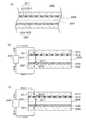
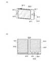
図1(A)に、蓄電装置2200の構造の一部を示す。蓄電装置2200は、正極2201と、正極2201と電解質2207を介して設けられた負極2211と、を有している。FIG. 1A illustrates part of the structure of the
正極2201は、集電体2203と、集電体2203上に設けられた正極活物質層2205と、で構成される。集電体2203の材料としては、例えば、白金、銅、またはチタン、アルミニウム等の導電性材料を用いることができる。正極活物質層2205の材料としては、実施の形態1で示した材料を用いることができる。正極活物質層2205の材料及び作製方法は、実施の形態1に準じればよい。The
負極2211は、集電体2213と、集電体2213上に設けられた負極活物質層2215と、で構成されている。集電体2213の材料としては、例えば、白金、銅、又はチタン等の導電性材料を用いることができる。負極活物質層2215の材料としては、例えば、黒鉛等の炭素材料、リチウム金属、シリコン等を用いることができる。The
電解質2207は、反応物質(リチウムイオン等)を伝導する機能を有する。電解質2207の材料としては、固体または液体を用いることができる。電解質2207の材料が固体の場合は、例えば、Li3PO4、Li3PO4に窒素を混ぜたLixPOyNz(x、y、zは正の実数)、Li2S−SiS2、Li2S−P2S5、Li2S−B2S3等を用いることができる。また、これらにLiIなどをドープしたものも用いることができる。また、電解質2207の材料が液体の場合、溶媒と、溶媒に溶解される溶質(塩)とを含んでいる溶液を用いることができる。溶媒としては、例えば、プロピレンカーボネート、エチレンカーボネート等の環状カーボネート、または、ジメチルカーボネート、ジエチルカーボネート等の鎖状カーボネートを用いることができる。溶質(塩)としては、例えば、LiPF6、LiBF4、LiTFSA等の一または複数を含む軽金属塩を用いることができる。The
また、電解質2207が液体の場合は、セパレータ2209を設ける必要がある。セパレータ2209は、正極2201と負極2211との接触を防止するとともに、反応物質(リチウムイオン等)を通過させる機能を有する。セパレータ2209の材料としては、電解質2207に溶解しない材料、例えば、紙、不織布、ガラス繊維、ナイロン(ポリアミド等)、ビニロン(ポリビニルアルコール系繊維であり、ビナロンとも呼ぶ)、ポリプロピレン、ポリエステル、アクリル、ポリオレフィン、ポリウレタン等を用いることができる。また、電解質2207に固体電解質を適用した場合でも、セパレータ2209を設ける構成とすることも可能である。In addition, when the
次に、蓄電装置としてリチウムイオン二次電池を用いた場合の充放電の一例を、図1(B)及び図1(C)を用いて説明する。Next, an example of charging and discharging when a lithium ion secondary battery is used as the power storage device will be described with reference to FIGS.
充電は、図1(B)に示すように、正極2201と負極2211との間に電源2221を接続することで行われる。電源2221から電圧が印加されると、正極2201のリチウムがイオン化し、リチウムイオン2217として正極2201から脱離されるとともに、電子2219が発生する。リチウムイオン2217は、電解質2207を介して負極2211に移動する。電子2219は、電源2221を介して負極2211に移動する。そして、リチウムイオン2217は、負極2211で電子2219を受け取り、リチウムとして負極2211に挿入される。Charging is performed by connecting a
一方、放電は、図1(C)に示すように、正極2201と負極2211の間に負荷2223を接続することで行われる。負極2211のリチウムがイオン化し、リチウムイオン2217として負極2211から脱離されるとともに、電子2219が発生する。リチウムイオン2217は、電解質2207を介して正極2201に移動する。電子2219は、負荷2223を介して正極2201に移動する。そして、リチウムイオン2217は、正極2201で電子2219を受け取り、リチウムとして正極2201に挿入される。On the other hand, discharge is performed by connecting a
以上のように、リチウムイオンが正極2201及び負極2211間を移動することで、充放電が行われる。蓄電装置2200の正極2201において、正極活物質層2205に実施の形態1で示した材料を適用する。As described above, the lithium ions move between the
材料を合成する際にフラックスを用いることで、低温及び短時間での熱処理が可能となり、電極用材料の粒子の拡大を抑えることができる。そのため、リチウムイオン二次電池として、粒子の拡大が抑えられた材料で作製される電極を用いる場合、リチウムイオンに充分な速さが得られ、高速充放電が可能となり、蓄電装置の特性を向上させることができる。また、低温および短時間での熱処理が可能となることで、製造コストを低減できる。By using a flux when synthesizing the material, heat treatment can be performed at a low temperature and in a short time, and expansion of particles of the electrode material can be suppressed. Therefore, when using an electrode made of a material that suppresses the expansion of particles as a lithium ion secondary battery, sufficient speed can be obtained for lithium ions, high-speed charging / discharging is possible, and the characteristics of the power storage device are improved. Can be made. In addition, since the heat treatment can be performed at a low temperature and in a short time, the manufacturing cost can be reduced.
なお、本実施の形態は、他の実施の形態と適宜組み合わせて実施することができる。Note that this embodiment can be implemented in combination with any of the other embodiments as appropriate.
(実施の形態3)
本実施の形態では、実施の形態2と異なる構成の蓄電装置について、図2乃至図4を用いて説明する。(Embodiment 3)
In this embodiment, a power storage device having a structure different from that in Embodiment 2 is described with reference to FIGS.
蓄電装置の負極活物質層として、黒鉛などの炭素材料が実用化されている。しかしながら、炭素材料は理論容量に限界があり、蓄電装置において実用化されている以上の高容量化は難しい。そこで、本実施の形態では、負極活物質層としてシリコン材料を用いることで、蓄電装置の特性向上を図る。また、正極活物質として実施の形態1で示した材料を用いることで、さらなる蓄電装置の特性向上を図る。A carbon material such as graphite has been put to practical use as a negative electrode active material layer of a power storage device. However, the theoretical capacity of the carbon material is limited, and it is difficult to increase the capacity beyond that practically used in the power storage device. Thus, in this embodiment, the characteristics of the power storage device are improved by using a silicon material for the negative electrode active material layer. Further, by using the material described in Embodiment 1 as the positive electrode active material, the characteristics of the power storage device can be further improved.
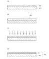
図2に負極の作製方法を示す。蓄電装置の構造は上記図1を適用することができる。また、本実施の形態に示す負極は、図1の負極2211に相当する。FIG. 2 shows a method for manufacturing a negative electrode. 1 can be applied to the structure of the power storage device. The negative electrode described in this embodiment corresponds to the
まず、負極集電体411上に、非晶質シリコン層413を形成する(図2(A)参照)。First, an
負極集電体411は、チタン、ニッケル、銅、インジウム、錫、または銀等の導電性の高い材料を用いることができる。本実施の形態では、負極集電体411にチタンを用いることとする。The negative electrode
非晶質シリコン層413は、例えば、プラズマCVD法、減圧CVD法、スパッタリング法、または真空蒸着法等を用いて、厚さ100nm以上5μm以下(好ましくは1μm以上3μm以下)の範囲で形成することができる。非晶質シリコン層413の膜厚が100nmより薄いと、結晶化後に得られる負極活物質層417の膜厚が薄すぎて、充放電ができない恐れがある。非晶質シリコン層413の膜厚が5μmより厚いと、非晶質シリコン層413を結晶化しきれない恐れがある。または、非晶質シリコン層413の膜厚が5μmより厚いと、結晶化後に得られる負極活物質層417が充放電の際に応力変化によってピーリングしてしまう恐れがある。したがって、非晶質シリコン層413の膜厚は上述の範囲内にすることが好ましい。The
次に、触媒元素415を非晶質シリコン層413に添加する(図2(B)参照)。Next, a
触媒元素415の添加方法は、例えば、塗布法、スパッタリング法、真空蒸着法等がある。上記方法を用いることで、非晶質シリコン層413の表面に直接付着させることができる。Examples of a method for adding the
触媒元素を非晶質シリコン層に添加することで、後に行う結晶化のプロセス温度の低温化及びプロセス時間の短縮化が可能となる。具体的には、結晶化のプロセス温度を50℃乃至100℃程度引き下げることが可能であり、プロセス時間を1/5乃至1/10程度まで短縮することが可能である。By adding the catalyst element to the amorphous silicon layer, it is possible to lower the process temperature of crystallization performed later and to shorten the process time. Specifically, the crystallization process temperature can be lowered by about 50 ° C. to 100 ° C., and the process time can be shortened to about 1/5 to 1/10.
触媒元素415としては、非晶質シリコンの結晶化を促進する元素、例えば、ニッケル(Ni)、銅(Cu)、インジウム(In)、スズ(Sn)、銀(Ag)等の一または複数の金属元素を用いることができる。ニッケルは、触媒元素として、効果や再現性の点において非常に優れている。触媒としてニッケルを用いた場合、非晶質シリコンを結晶化させる際にニッケルシリサイドを形成し、非晶質シリコンが結晶化する際の結晶核として機能する。本実施の形態では、触媒元素415としてニッケルを用いることとする。ニッケルを添加する具体的な方法を、図3を用いて以下に示す。As the
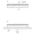
まず、負極集電体411上に形成された非晶質シリコン層413の表面に、触媒元素415を含む溶液416を添加する(図3(A)参照)。First, a
溶液416としては、例えば、酢酸ニッケル溶液、塩酸ニッケル溶液、硝酸ニッケル溶液、または硫酸ニッケル溶液等を用いることができる。本実施の形態では、溶液416として酢酸ニッケル溶液を用いることとする。As the
次に、スピナー421を用いてスピンドライを行う(図3(B)参照)。Next, spin drying is performed using a spinner 421 (see FIG. 3B).
スピンドライを行うことにより、非晶質シリコン層413表面に、均一に、触媒元素415を含む溶液416を保持させることができる。また、溶液416を添加する前に、非晶質シリコン層413表面に薄い酸化層を形成しておくことが好ましい。これは、非晶質シリコン層413表面が疎水性であるため、溶液416が水を含む溶液であると、溶液416が非晶質シリコン層413表面で弾かれ、触媒元素415が非晶質シリコン層413表面全体に添加できない恐れがあるからである。非晶質シリコン層413表面に薄い酸化層を形成することで、溶液416に対する濡れ性を高める(親水性にする)ことができる。酸化層を形成する方法としては、非晶質シリコン層413表面にUV光を照射する方法、または非晶質シリコン層413表面をアンモニア過水、オゾン水等で処理する方法等がある。このような方法で形成される酸化層は非常に薄いため、触媒元素415は酸化層を通って非晶質シリコン層413に到達することができる。By performing spin drying, the
以上のように、非晶質シリコン層413に、触媒元素415であるニッケルを添加することができる。As described above, nickel which is the
次に、触媒元素415が添加された非晶質シリコン層413に熱処理を行う(図2(C)参照)。Next, heat treatment is performed on the
非晶質シリコン層413を結晶化させるための熱処理方法は、例えば、加熱炉にて行う方法、レーザビーム等の光照射を行う方法等がある。加熱炉において熱処理を行う場合は、450℃以上750℃以下、好ましくは550℃以上620℃以下の温度範囲で行うことができる。また、熱処理時間は、1時間以上24時間以下、好ましくは4時間以上10時間以下の範囲で行うことができる。例えば、550℃、4時間の熱処理を行えばよい。また、レーザビームを照射して熱処理を行う場合は、例えば、エネルギー密度を100mJ/cm2以上400mJ/cm2以下、好ましくは200mJ/cm2以上400mJ/cm2以下の範囲、代表的には250mJ/cm2として行うことができる。例えば、KrFエキシマレーザのレーザビーム(波長248nm、パルス幅20nsec)を用いて、熱処理を行えばよい。As a heat treatment method for crystallizing the
上記熱処理によって、非晶質シリコン層413は結晶化し、結晶性シリコン層(負極活物質層417)となる(図2(D)参照)。By the heat treatment, the
熱処理によって得られた結晶性シリコン層は、負極活物質層として用いることができる。また、負極集電体411と、負極集電体411上に形成された結晶性シリコン層(負極活物質層417)は、負極419として用いることができる。負極活物質層として結晶性シリコンを用いることで、非晶質シリコンを用いた場合よりも反応物質(リチウムイオン等)の拡散速度が速く、蓄電装置の特性のさらなる向上に結びつけることができる。The crystalline silicon layer obtained by the heat treatment can be used as a negative electrode active material layer. The negative electrode
非晶質シリコン層413中の触媒元素415は、熱処理によって移動し、結晶核となって機能する。そのため、結晶化を促進させることができる。例えば、触媒元素415にニッケルを用いた場合、熱処理により、ニッケルと非晶質シリコンとが反応してニッケルシリサイドを形成し、ニッケルシリサイドが結晶核となってその後の結晶成長に寄与する。これにより、結晶化が促進され、結晶化のプロセス温度の低温化及びプロセス時間の短縮化が可能となる。また結晶化のプロセス温度の低温化及びプロセス時間の短縮化が可能となることで、製造コスト削減及び生産性向上に寄与することができる。The
また、結晶性シリコン層に残留する触媒元素415は、導電性を有する金属元素であるため、除去する必要はない。Further, the
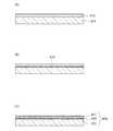
熱処理後、結晶性シリコン層(負極活物質層417)の最表面に触媒元素が偏析する場合がある。この場合、結晶性シリコン層においては、深さ方向(膜厚方向)において、表面に近いほど、触媒元素415の濃度が高くなる。また、触媒元素415は熱処理により酸化され、導電性酸化物となる。例えば、触媒元素415としてニッケル、銅、インジウム、スズ、または銀等を用いた場合、結晶性シリコン層の最表面に酸化ニッケル、酸化銅、酸化インジウム、酸化スズ、または酸化銀等が偏析する。After the heat treatment, the catalytic element may segregate on the outermost surface of the crystalline silicon layer (negative electrode active material layer 417). In this case, in the crystalline silicon layer, the concentration of the
図4に、負極活物質層417(結晶性シリコン層)の最表面に導電性酸化物418が偏析している様子を示す。図4(A)は、導電性酸化物418が負極活物質層417の最表面に粒子状に偏析している様子を示している。図4(B)は、導電性酸化物418が負極活物質層417の最表面に層状に偏析している様子を示す。導電性酸化物418には導電性があるため、負極活物質層417の導電性を高めることができる。FIG. 4 shows a state where the
以上のように、負極活物質層として結晶性シリコン層が適用された負極419を作製することができる。As described above, the
蓄電装置の正極は、実施の形態1で示した電極用材料を用いて作製することとする。電極用材料を合成する際にフラックスを用いることで、低温及び短時間での熱処理が可能となり、電極用材料の粒子の拡大を抑えることができる。そのため、リチウムイオン二次電池として、粒子の拡大が抑えられた材料で作製される電極を用いる場合、リチウムイオンに充分な速さが得られ、高速充放電が可能となり、蓄電装置の特性を向上させることができる。また、低温および短時間での熱処理が可能となることで、製造コストを低減できる。正極の作製方法等は、実施の形態1を参照すればよい。また、電解質は実施の形態2を参照すればよい。The positive electrode of the power storage device is manufactured using the electrode material described in Embodiment 1. By using a flux when synthesizing the electrode material, heat treatment can be performed at a low temperature and in a short time, and expansion of particles of the electrode material can be suppressed. Therefore, when using an electrode made of a material that suppresses the expansion of particles as a lithium ion secondary battery, sufficient speed can be obtained for lithium ions, high-speed charging / discharging is possible, and the characteristics of the power storage device are improved. Can be made. In addition, since the heat treatment can be performed at a low temperature and in a short time, the manufacturing cost can be reduced. Embodiment 1 may be referred to for the manufacturing method and the like of the positive electrode. For the electrolyte, Embodiment Mode 2 may be referred to.
以上より、本実施の形態で示した負極および実施の形態1で示した正極を用いることで、高速充放電が可能な蓄電装置を作製することができる。As described above, by using the negative electrode described in this embodiment and the positive electrode described in Embodiment 1, a power storage device capable of high-speed charge / discharge can be manufactured.
なお、本実施の形態は、他の実施の形態と適宜組み合わせることができる。Note that this embodiment can be combined with any of the other embodiments as appropriate.
(実施の形態4)
本実施の形態では、実施の形態2及び実施の形態3と異なる構成の蓄電装置について説明する。(Embodiment 4)
In this embodiment, a power storage device having a structure different from those in Embodiment 2 and Embodiment 3 will be described.
実施の形態3では、負極集電体411上に非晶質シリコン層413を形成し、非晶質シリコン層413に触媒元素415を添加した後、熱処理により結晶化させることで、負極活物質層417となる結晶性シリコン層を得る例を示した。本実施の形態では、負極集電体そのものを触媒元素として利用し、負極活物質層となる結晶性シリコン層を形成する例について説明する。In Embodiment 3, the
まず、負極集電体451上に、非晶質シリコン層453を形成する(図5(A)参照)。First, an
負極集電体451は、非晶質シリコン層の結晶化を促進する一または複数の触媒元素を含み、且つ、導電性を有する材料を用いる。触媒元素は、実施の形態3を参照すればよい。また、負極集電体451は、触媒元素の単体を用いてもよいし、触媒元素と他の材料との合金を用いてもよい。負極集電体451を合金とする場合は、リチウムと合金を作らない材料を選択することが好ましい。リチウムと合金を作る材料を用いると、負極集電体451自体の安定性が低下する恐れがある。The negative electrode
非晶質シリコン層453は、実施の形態3で示した非晶質シリコン層413と同様に作製することができる。The
次に、非晶質シリコン層453に熱処理を行い、結晶性シリコン層(負極活物質層457)を形成する(図5(B)参照)。Next, heat treatment is performed on the
熱処理によって結晶化した結晶性シリコン層は、負極活物質層として用いることができる。また、負極集電体451と、負極集電体451上に形成された結晶性シリコン層(負極活物質層457)は、負極459として用いることができる。The crystalline silicon layer crystallized by the heat treatment can be used as the negative electrode active material layer. The negative electrode
非晶質シリコン層453の熱処理により、負極集電体451に含まれる触媒元素は、負極集電体451から非晶質シリコン層453中に熱拡散して移動する。これにより、非晶質シリコン層453の結晶成長が、負極集電体451との界面から他方の面に向かって進行する。非晶質シリコン層453の深さ方向(膜厚方向)において、下(負極集電体451との界面)から上(他方の面)へ結晶成長が進行する。このため、得られた結晶性シリコン層は、深さ方向において、下から上に向かうほど、触媒元素の濃度が低い。By the heat treatment of the
熱処理条件等は、実施の形態3で示した非晶質シリコン層413の熱処理条件を参照すればよい。本実施の形態では、負極集電体451が触媒元素として作用するため、結晶化のプロセス温度の低温化及びプロセス時間の短縮化が可能となる。そして、製造コスト削減及び生産性向上に寄与することができる。For the heat treatment conditions and the like, the heat treatment conditions for the
また、本実施の形態では、負極集電体451自体が触媒元素として作用するため、触媒元素を添加する工程が不要となり、この点からも製造コスト削減及び生産性向上に寄与することができる。Further, in this embodiment, since the negative electrode
また、負極活物質層457(結晶性シリコン層)に残留する触媒元素は、導電性を有する金属元素であるため、除去する必要はない。Further, the catalyst element remaining in the negative electrode active material layer 457 (crystalline silicon layer) is a metal element having conductivity, and thus does not need to be removed.
以上のように、負極活物質層として結晶性シリコン層が適用された負極459を作製することができる。As described above, the
蓄電装置の正極は、実施の形態1で示した電極用材料を用いて作製することとする。電極用材料を合成する際にフラックスを用いることで、低温及び短時間での熱処理が可能となり、電極用材料の粒子の拡大を抑えることができる。そのため、リチウムイオン二次電池として、粒子の拡大が抑えられた材料で作製される電極を用いる場合、リチウムイオンに充分な速さが得られ、高速充放電が可能となり、蓄電装置の特性を向上させることができる。また、低温および短時間での熱処理が可能となることで、製造コストを低減できる。正極の作製方法等は、実施の形態1を参照すればよい。また、電解質は実施の形態2を参照すればよい。The positive electrode of the power storage device is manufactured using the electrode material described in Embodiment 1. By using a flux when synthesizing the electrode material, heat treatment can be performed at a low temperature and in a short time, and expansion of particles of the electrode material can be suppressed. Therefore, when using an electrode made of a material that suppresses the expansion of particles as a lithium ion secondary battery, sufficient speed can be obtained for lithium ions, high-speed charging / discharging is possible, and the characteristics of the power storage device are improved. Can be made. In addition, since the heat treatment can be performed at a low temperature and in a short time, the manufacturing cost can be reduced. Embodiment 1 may be referred to for the manufacturing method and the like of the positive electrode. For the electrolyte, Embodiment Mode 2 may be referred to.
以上より、本実施の形態で示した負極および実施の形態1で示した正極を用いることで、高速充放電が可能な蓄電装置を作製することができる。As described above, by using the negative electrode described in this embodiment and the positive electrode described in Embodiment 1, a power storage device capable of high-speed charge / discharge can be manufactured.
なお、本実施の形態は、他の実施の形態と適宜組み合わせることができる。Note that this embodiment can be combined with any of the other embodiments as appropriate.
(実施の形態5)
本実施の形態では、実施の形態2乃至実施の形態4と異なる構成の蓄電装置について説明する。(Embodiment 5)
In this embodiment, a power storage device having a structure different from those in Embodiments 2 to 4 is described.
本実施の形態では、集電体と、集電体材料及び活物質材料の混合層と、活物質層と、で負極を構成する。集電体には金属材料を用い、負極活物質層にはシリコン材料を用い、混合層は、金属材料とシリコン材料の混合層を用いることとする。In this embodiment, the current collector, the mixed layer of the current collector material and the active material, and the active material layer form a negative electrode. A metal material is used for the current collector, a silicon material is used for the negative electrode active material layer, and a mixed layer of the metal material and the silicon material is used for the mixed layer.
負極活物質層として用いるシリコン材料は、炭素材料よりも理論的に容量を大きくすることが可能なため、蓄電装置の容量を高容量化することができ、蓄電装置の特性向上を図ることができる。Since the silicon material used as the negative electrode active material layer can theoretically have a larger capacity than the carbon material, the capacity of the power storage device can be increased and the characteristics of the power storage device can be improved. .
集電体と負極活物質層との間に集電体材料と活物質層材料との混合層を設けることで、集電体と活物質層との密着性や電子授受の容易性等を高めることができる。そのため、さらに、蓄電装置の特性向上を図ることができる。By providing a mixed layer of the current collector material and the active material layer material between the current collector and the negative electrode active material layer, the adhesion between the current collector and the active material layer, the ease of electron transfer, and the like are improved. be able to. Therefore, the characteristics of the power storage device can be further improved.
正極活物質としては、実施の形態1に示した材料を用いることとする。As the positive electrode active material, the material described in Embodiment 1 is used.
負極の作製方法について、図6を用いて説明する。蓄電装置の構造としては図1を適用できる。また、本実施の形態で作製する負極は、図1の負極2211に相当する。A method for manufacturing the negative electrode will be described with reference to FIGS. As a structure of the power storage device, FIG. 1 can be applied. Further, the negative electrode manufactured in this embodiment corresponds to the
まず、負極集電体471上に、非晶質シリコン層473を形成する(図6(A)参照)。First, an
負極集電体471としては、チタン、ニッケル、銅、インジウム、錫、又は銀等の導電性材料を用いることができる。As the negative electrode
非晶質シリコン層473は、実施の形態3に示した非晶質シリコン層413と同様に形成することができる。The
次に、非晶質シリコン層473を有した集電体の熱処理を行い、集電体材料と活物質材料との間に、混合層475を形成する(図6(B)参照)。Next, heat treatment is performed on the current collector including the
負極集電体471として、例えば、チタンを用いた場合、混合層475は、チタンとシリコンの混合層を形成する。チタンとシリコンの混合層は、チタンシリサイド層であってもよい。For example, when titanium is used as the negative electrode
上述した熱処理において、非晶質シリコン層473を結晶化し、結晶性シリコン層(負極活物質層477)を形成してもよい。熱処理によって結晶化した結晶性シリコン層は、負極活物質層として用いることができる。また、負極集電体471と、混合層475と、結晶性シリコン層(負極活物質層477)と、は負極479として用いることができる。(図6(C)参照)。In the heat treatment described above, the
なお、図6(B)における熱処理は、混合層475を形成する目的で行う。この熱処理で、非晶質シリコン層473が所望の結晶性まで結晶化されなければ、さらに結晶化のための熱処理(レーザビーム照射も含む)を行ってもよい。また、負極活物質層477は、非晶質シリコンや微結晶シリコンを用いてもよい。Note that the heat treatment in FIG. 6B is performed for the purpose of forming the
負極活物質層477として結晶性シリコンを用いることで、非晶質シリコンを用いた場合よりもリチウムイオン等の拡散速度が速く、蓄電装置の特性向上に寄与できるため好ましい。It is preferable to use crystalline silicon for the negative electrode
以上のように、負極活物質層として結晶性シリコン層が適用された負極479を作製することができる。As described above, the
蓄電装置の正極は、実施の形態1で示した電極用材料を用いて作製することとする。電極用材料を合成する際にフラックスを用いることで、低温及び短時間での熱処理が可能となり、電極用材料の拡大を抑えることができる。そのため、リチウムイオン二次電池として、粒子の拡大が抑えられた材料で作製される電極を用いる場合、リチウムイオンに充分な速さが得られ、高速充放電が可能となり、蓄電装置の特性を向上させることができる。また、低温および短時間での熱処理が可能となることで、製造コストを低減できる。正極の作製方法等は、実施の形態1を参照すればよい。また、電解質は実施の形態2を参照すればよい。The positive electrode of the power storage device is manufactured using the electrode material described in Embodiment 1. By using a flux when synthesizing the electrode material, heat treatment can be performed at a low temperature and in a short time, and expansion of the electrode material can be suppressed. Therefore, when using an electrode made of a material that suppresses the expansion of particles as a lithium ion secondary battery, sufficient speed can be obtained for lithium ions, high-speed charging / discharging is possible, and the characteristics of the power storage device are improved. Can be made. In addition, since the heat treatment can be performed at a low temperature and in a short time, the manufacturing cost can be reduced. Embodiment 1 may be referred to for the manufacturing method and the like of the positive electrode. For the electrolyte, Embodiment Mode 2 may be referred to.
以上より、本実施の形態で示した負極および実施の形態1で示した正極を用いることで、高速充放電が可能な蓄電装置を作製することができる。また、本実施の形態では、集電体と活物質層との間に混合層を形成しているため、集電体と活物質層との界面の特性(密着性、電子授受の容易性等)を向上させることができる。As described above, by using the negative electrode described in this embodiment and the positive electrode described in Embodiment 1, a power storage device capable of high-speed charge / discharge can be manufactured. In this embodiment, since a mixed layer is formed between the current collector and the active material layer, characteristics of the interface between the current collector and the active material layer (adhesion, ease of electron transfer, etc.) ) Can be improved.
なお、本実施の形態は、他の実施の形態と適宜組み合わせることができる。Note that this embodiment can be combined with any of the other embodiments as appropriate.
(実施の形態6)
本実施の形態では、本発明の一態様に係る蓄電装置の応用形態について説明する。(Embodiment 6)
In this embodiment, an application mode of the power storage device according to one embodiment of the present invention will be described.
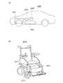
蓄電装置は、さまざまな電子機器に搭載することができる。例えば、デジタルカメラやビデオカメラ等のカメラ類、携帯電話機、携帯情報端末、電子書籍用端末、携帯型ゲーム機、デジタルフォトフレーム、音響再生装置等に搭載することができる。また、蓄電装置は、電気自動車、ハイブリッド自動車、鉄道用電気車両、電動式作業車、電動式カート、電動式車椅子、又は電気自転車等の電気推進車両に搭載することができる。The power storage device can be mounted on various electronic devices. For example, it can be mounted on a camera such as a digital camera or a video camera, a mobile phone, a portable information terminal, an electronic book terminal, a portable game machine, a digital photo frame, an audio playback device, or the like. The power storage device can be mounted on an electric propulsion vehicle such as an electric vehicle, a hybrid vehicle, a railway electric vehicle, an electric work vehicle, an electric cart, an electric wheelchair, or an electric bicycle.
本発明の一態様に係る蓄電装置は、高容量化、充放電速度の向上などの特性向上が図られている。蓄電装置の特性を向上させることで、蓄電装置の小型軽量化にも結びつけることができる。このような蓄電装置を搭載することで、電子機器や電気推進車両などの充電時間の短縮、使用時間の延長、小型軽量化などが可能となり、利便性やデザイン性の向上も実現できる。The power storage device according to one embodiment of the present invention has improved characteristics such as an increase in capacity and an increase in charge / discharge speed. By improving the characteristics of the power storage device, the power storage device can be reduced in size and weight. By mounting such a power storage device, it is possible to shorten the charging time, extend the usage time, reduce the size and weight of electronic devices and electric propulsion vehicles, and improve convenience and design.
図7(A)は、携帯電話機の一例を示している。携帯電話機3010は、筐体3011に表示部3012が組み込まれている。筐体3011は、さらに操作ボタン3013、操作ボタン3017、外部接続ポート3014、スピーカー3015、及びマイク3016等を備えている。このような携帯電話機に、本発明の一態様に係る蓄電装置を搭載することで、利便性やデザイン性を向上させることができる。FIG. 7A illustrates an example of a mobile phone. A
図7(B)は、電子書籍用端末の一例を示している。電子書籍用端末3030は、第1の筐体3031及び第2の筐体3033の2つの筐体で構成されて、2つの筐体が軸部3032により一体にされている。第1の筐体3031及び第2の筐体3033は、軸部3032を軸として開閉動作を行うことができる。第1の筐体3031には第1の表示部3035が組み込まれ、第2の筐体3033には第2の表示部3037が組み込まれている。その他、第2の筐体3033に、操作ボタン3039、電源3043、及びスピーカー3041等を備えている。このような電子書籍用端末に、本発明の一態様に係る蓄電装置を搭載することで、利便性やデザイン性を向上させることができる。FIG. 7B illustrates an example of an electronic book terminal. The
図8(A)は、電気自動車の一例を示している。電気自動車3050には、蓄電装置3051が搭載されている。蓄電装置3051の電力は、制御回路3053により出力が調整されて、駆動装置3057に供給される。制御回路3053は、コンピュータ3055によって制御される。FIG. 8A illustrates an example of an electric vehicle. An
駆動装置3057は、直流電動機若しくは交流電動機単体、又は電動機と内燃機関と、を組み合わせて構成される。コンピュータ3055は、電気自動車3050の運転者の操作情報(加速、減圧、停止など)や走行時の情報(登坂や下坂等の情報、駆動輪にかかる負荷情報など)の入力情報に基づき、制御回路3053に制御信号を出力する。制御回路3053は、コンピュータ3055の制御信号により、蓄電装置3051から供給される電気エネルギーを調整して駆動装置3057への出力を制御する。交流電動機を搭載している場合は、直流を交流に変換するインバータも内蔵される。The
蓄電装置3051は、プラグイン技術による外部からの電力供給により充電することができる。蓄電装置3051として、本発明の一態様に係る蓄電装置を搭載することで、充電時間の短縮化などに寄与することができ、利便性を向上させることができる。また、充放電速度の向上により、電気自動車の加速力向上に寄与することができ、電気自動車の性能向上に寄与することができる。また、蓄電装置3051の特性向上により、蓄電装置3051自体を小型軽量化できれば、車両の軽量化に寄与することができ、燃費向上にも結びつけることができる。The
図8(B)は、電動式の車椅子の一例を示している。車椅子3070は、蓄電装置、電力制御部、制御手段等を有する制御部3073を備えている。制御部3073により出力が調整された蓄電装置の電力は、駆動部3075に供給される。また、制御部3073は、コントローラ3077と接続されている。コントローラ3077の操作により、制御部3073を介して駆動部3075が駆動させることができ、車椅子3070の前進、後進、旋回等の動作や速度を制御することができる。FIG. 8B illustrates an example of an electric wheelchair. The
車椅子3070の蓄電装置についても、プラグイン技術による外部からの電力供給により充電することができる。制御部3073の蓄電装置として、本発明の一態様に係る蓄電装置を搭載することで、充電時間の短縮化などに寄与することができ、利便性を向上させることができる。また、蓄電装置の特性向上により、蓄電装置自体を小型軽量化できれば、車椅子3070の使用者及び介助者の使い易さを高めることができる。The power storage device of the
なお、電気推進車両として鉄道用電気車両に蓄電装置を搭載させる場合、架線や導電軌条からの電力供給により充電することも可能である。In addition, when mounting an electrical storage apparatus in the railway electric vehicle as an electric propulsion vehicle, it is also possible to charge by supplying electric power from an overhead wire or a conductive rail.
本実施の形態は、他の実施の形態と適宜組み合わせることができる。This embodiment can be combined with any of the other embodiments as appropriate.
411 負極集電体
413 非晶質シリコン層
415 触媒元素
416 溶液
417 負極活物質層
418 導電性酸化物
419 負極
421 スピナー
451 負極集電体
453 非晶質シリコン層
457 負極活物質層
459 負極
471 負極集電体
473 非晶質シリコン層
475 混合層
477 負極活物質層
479 負極
2200 蓄電装置
2201 正極
2203 集電体
2205 正極活物質層
2207 電解質
2209 セパレータ
2211 負極
2213 集電体
2215 負極活物質層
2217 リチウムイオン
2219 電子
2221 電源
2223 負荷
3010 携帯電話機
3011 筐体
3012 表示部
3013 操作ボタン
3014 外部接続ポート
3015 スピーカー
3016 マイク
3017 操作ボタン
3030 電子書籍用端末
3031 第1の筐体
3032 軸部
3033 第2の筐体
3035 第1の表示部
3037 第2の表示部
3039 操作ボタン
3041 スピーカー
3043 電源
3050 電気自動車
3051 蓄電装置
3053 制御回路
3055 コンピュータ
3057 駆動装置
3070 車椅子
3073 制御部
3075 駆動部
3077 コントローラ411 Negative electrode
Claims (2)
Translated fromJapanese前記一般式のAの供給源と成る化合物、前記一般式のMの供給源と成る化合物、及び前記一般式のSiの供給源と成る化合物を混合して、混合材料を作製し、
前記混合材料に対して、第1の熱処理を行い、粉砕した後、フラックスを混合し、
前記フラックスを混合した混合材料に対して、第2の熱処理を行い、
前記第1の熱処理は、不活性ガス雰囲気において、250℃以上400℃以下の温度で、1時間以上20時間以下行い、
前記第2の熱処理は、不活性ガス雰囲気において、前記第1の熱処理温度以上700℃以下の温度で、1時間以上20時間以下行い、
前記フラックスは、塩化リチウム、塩化ナトリウム、塩化カリウム、塩化ルビジウム、塩化カルシウム、塩化マグネシウムの一または複数の化合物である電極用材料の作製方法。An electrode material comprising a compound represented by the general formula A2-a MSiO4 (A represents Li, M represents any of iron, manganese, cobalt, and nickel, and a represents 0 or more and less than 2). A production method comprising:
A compound that is a source of A in the general formula, a compound that is a source of M in the general formula, and a compound that is a source of Si in the general formula are mixed to prepare a mixed material,
The mixed materialis subjected to a first heat treatment, pulverized, and then mixed with a flux.
Asecond heat treatment is performed on the mixed material mixed with the flux,
The first heat treatment is performed in an inert gas atmosphere at a temperature of 250 ° C. to 400 ° C. for 1 hour to 20 hours,
The second heat treatment is performed in an inert gas atmosphere at a temperature of the first heat treatment temperature to 700 ° C. for 1 hour to 20 hours,
The method for producing an electrode material, wherein the flux is one or more compounds of lithium chloride, sodium chloride, potassium chloride, rubidium chloride, calcium chloride, and magnesium chloride.
Priority Applications (1)
| Application Number | Priority Date | Filing Date | Title |
|---|---|---|---|
| JP2011139983AJP5917027B2 (en) | 2010-06-30 | 2011-06-24 | Method for producing electrode material |
Applications Claiming Priority (3)
| Application Number | Priority Date | Filing Date | Title |
|---|---|---|---|
| JP2010149417 | 2010-06-30 | ||
| JP2010149417 | 2010-06-30 | ||
| JP2011139983AJP5917027B2 (en) | 2010-06-30 | 2011-06-24 | Method for producing electrode material |
Publications (2)
| Publication Number | Publication Date |
|---|---|
| JP2012033473A JP2012033473A (en) | 2012-02-16 |
| JP5917027B2true JP5917027B2 (en) | 2016-05-11 |
Family
ID=45398999
Family Applications (1)
| Application Number | Title | Priority Date | Filing Date |
|---|---|---|---|
| JP2011139983AExpired - Fee RelatedJP5917027B2 (en) | 2010-06-30 | 2011-06-24 | Method for producing electrode material |
Country Status (2)
| Country | Link |
|---|---|
| US (1) | US8715525B2 (en) |
| JP (1) | JP5917027B2 (en) |
Families Citing this family (5)
| Publication number | Priority date | Publication date | Assignee | Title |
|---|---|---|---|---|
| CN103733396B (en)* | 2012-08-08 | 2016-06-29 | 北京科瑞沅科技有限公司 | Doping secondary battery positive electrode material and preparation method thereof |
| US20160043394A1 (en)* | 2013-03-15 | 2016-02-11 | E.I. Du Pont De Nemours And Company | Cathode synthesized by flux method and battery comprising same |
| WO2016164617A1 (en) | 2015-04-07 | 2016-10-13 | Brown University | Cation energy storage device and methods |
| US10707522B2 (en) | 2015-09-24 | 2020-07-07 | Ford Global Technologies, Llc | Methods of manufacturing a solid state battery |
| CN111647863B (en)* | 2020-07-02 | 2022-03-25 | 河北大学 | Li2FexSiO4Preparation method and application of positive electrode film |
Family Cites Families (67)
| Publication number | Priority date | Publication date | Assignee | Title |
|---|---|---|---|---|
| JPS5277899A (en)* | 1975-12-23 | 1977-06-30 | Agency Of Ind Science & Technol | Production of lithium ferrosilicate single crystal |
| JP2741814B2 (en) | 1991-12-26 | 1998-04-22 | シャープ株式会社 | Method for producing tantalum metal thin film |
| JP3364968B2 (en) | 1992-09-01 | 2003-01-08 | 株式会社デンソー | Battery |
| US5770018A (en) | 1996-04-10 | 1998-06-23 | Valence Technology, Inc. | Method for preparing lithium manganese oxide compounds |
| CN1042377C (en) | 1996-05-10 | 1999-03-03 | 中国科学院物理研究所 | Method for synthetizing positive electrode material in lithium ion battery |
| US5720859A (en) | 1996-06-03 | 1998-02-24 | Raychem Corporation | Method of forming an electrode on a substrate |
| US6348182B1 (en) | 1996-06-27 | 2002-02-19 | The Honjo Chemical Corporation | Process for producing lithium manganese oxide with spinel structure |
| JP3417523B2 (en) | 1996-10-29 | 2003-06-16 | 本荘ケミカル株式会社 | Method for producing lithium / manganese composite oxide for lithium secondary battery 3V class positive electrode material |
| JPH1125983A (en) | 1997-07-04 | 1999-01-29 | Japan Storage Battery Co Ltd | Active material for lithium battery |
| US5951831A (en) | 1997-07-11 | 1999-09-14 | Albright & Wilson Americas Limited | Condensation polymerization of phosphorus containing compounds |
| EP2219253B1 (en) | 1998-09-18 | 2015-06-10 | Canon Kabushiki Kaisha | Electrode material |
| JP2001167762A (en) | 1999-12-08 | 2001-06-22 | Tohoku Techno Arch Co Ltd | Lithium ion battery |
| US6962613B2 (en) | 2000-03-24 | 2005-11-08 | Cymbet Corporation | Low-temperature fabrication of thin-film energy-storage devices |
| CA2320661A1 (en) | 2000-09-26 | 2002-03-26 | Hydro-Quebec | New process for synthesizing limpo4 materials with olivine structure |
| EP1430555A2 (en) | 2001-04-06 | 2004-06-23 | Valence Technology, Inc. | Sodium ion batteries |
| US20040241540A1 (en) | 2001-09-19 | 2004-12-02 | Kazuo Tsutsumi | Three-dimensional cell and its electrode structure and method for manufacturing electrode material of three-dimensional cell |
| EP1456895B1 (en) | 2001-12-21 | 2017-03-29 | Massachusetts Institute Of Technology | Conductive lithium storage electrode |
| JP2003257429A (en) | 2002-03-04 | 2003-09-12 | Mitsui Mining & Smelting Co Ltd | Preparation method of iron-containing olivin manganese lithium phosphate and battery using the same |
| US20090220838A9 (en) | 2002-04-04 | 2009-09-03 | Jeremy Barker | Secondary electrochemical cell |
| US20040016632A1 (en) | 2002-07-26 | 2004-01-29 | Jeremy Barker | Methods of making transition metal compounds useful as cathode active materials using electromagnetic radiation |
| JP4058680B2 (en) | 2002-08-13 | 2008-03-12 | ソニー株式会社 | Method for producing positive electrode active material and method for producing non-aqueous electrolyte secondary battery |
| JP4089354B2 (en) | 2002-08-30 | 2008-05-28 | 株式会社Sumco | Epitaxial wafer and manufacturing method thereof |
| JP4822416B2 (en) | 2003-01-31 | 2011-11-24 | 三井造船株式会社 | Positive electrode material for secondary battery, method for producing the same, and secondary battery |
| JP4225859B2 (en) | 2003-07-29 | 2009-02-18 | 日本化学工業株式会社 | Method for producing lithium iron phosphorus composite oxide carbon composite containing Mn atom |
| US7307248B2 (en) | 2003-12-09 | 2007-12-11 | Cem Corporation | Method and apparatus for microwave assisted high throughput high pressure chemical synthesis |
| US7060238B2 (en) | 2004-03-04 | 2006-06-13 | Valence Technology, Inc. | Synthesis of metal phosphates |
| CA2567032A1 (en) | 2004-03-24 | 2005-10-13 | H.C. Starck, Inc. | Methods of forming alpha and beta tantalum films with controlled and new microstructures |
| JP4843918B2 (en) | 2004-08-26 | 2011-12-21 | 新神戸電機株式会社 | Composite oxide material and positive electrode active material for lithium secondary battery |
| US20070160519A1 (en) | 2005-03-28 | 2007-07-12 | Jeremy Barker | Method Of Making Active Materials For Use In Secondary Electrochemical Cells |
| EP1722428A1 (en) | 2005-05-13 | 2006-11-15 | Süd-Chemie Ag | Lithium secondary battery and electrodes for use therein |
| JP5084131B2 (en) | 2005-10-28 | 2012-11-28 | トヨタ自動車株式会社 | Method for producing LiMnPO4 |
| JP4691711B2 (en) | 2006-03-20 | 2011-06-01 | 独立行政法人産業技術総合研究所 | Lithium manganese composite oxide and method for producing the same |
| JP5235282B2 (en) | 2006-06-16 | 2013-07-10 | 国立大学法人九州大学 | Cathode active material and battery for non-aqueous electrolyte secondary battery |
| CA2566906A1 (en) | 2006-10-30 | 2008-04-30 | Nathalie Ravet | Carbon-coated lifepo4 storage and handling |
| US8066916B2 (en) | 2006-12-22 | 2011-11-29 | Umicore | Synthesis of crystalline nanometric LiFeMPO4 |
| JP5156946B2 (en)* | 2007-03-07 | 2013-03-06 | 国立大学法人九州大学 | Method for producing positive electrode active material for secondary battery |
| KR20090125268A (en)* | 2007-03-27 | 2009-12-04 | 고쿠리츠다이가쿠호진 토쿄고교 다이가꾸 | Manufacturing Method of Positive Electrode Material for Secondary Battery |
| JP2008260666A (en) | 2007-04-13 | 2008-10-30 | Kyushu Univ | Sodium secondary battery active material and method for producing the same |
| JP4798507B2 (en) | 2007-05-18 | 2011-10-19 | 独立行政法人産業技術総合研究所 | Method for producing single-crystal LiMn2O4 nanowire and high-rate Li-ion battery using single-crystal LiMn2O4 nanowire |
| JP5293936B2 (en) | 2007-05-21 | 2013-09-18 | 戸田工業株式会社 | Non-aqueous electrolyte secondary battery olivine-type composite oxide, method for producing the same, and secondary battery |
| JP2009004289A (en) | 2007-06-25 | 2009-01-08 | Panasonic Corp | Nonaqueous electrolyte secondary battery |
| JP5157365B2 (en) | 2007-10-25 | 2013-03-06 | 株式会社豊田中央研究所 | Lithium ion secondary battery and electric vehicle power source using the same |
| JP4595987B2 (en) | 2007-10-25 | 2010-12-08 | トヨタ自動車株式会社 | Cathode active material |
| US20090117020A1 (en) | 2007-11-05 | 2009-05-07 | Board Of Regents, The University Of Texas System | Rapid microwave-solvothermal synthesis and surface modification of nanostructured phospho-olivine cathodes for lithium ion batteries |
| JP5316809B2 (en) | 2007-11-13 | 2013-10-16 | 住友電気工業株式会社 | Lithium battery and manufacturing method thereof |
| JP5109619B2 (en) | 2007-11-21 | 2012-12-26 | トヨタ自動車株式会社 | Battery pack system and charge / discharge control method |
| JP2009129179A (en) | 2007-11-22 | 2009-06-11 | Toshiba Corp | Program parallelization support apparatus and program parallelization support method |
| EP2065887A1 (en) | 2007-11-30 | 2009-06-03 | Hitachi Global Storage Technologies Netherlands B.V. | Method for manufacturing magnetic disk unit |
| JP5383217B2 (en) | 2008-01-28 | 2014-01-08 | 住友化学株式会社 | Positive electrode active material, sodium secondary battery, and olivine-type phosphate production method |
| JP5517032B2 (en) | 2008-03-31 | 2014-06-11 | 戸田工業株式会社 | Non-aqueous electrolyte secondary battery olivine-type composite oxide particle powder, method for producing the same, and secondary battery |
| JP4662183B2 (en) | 2008-04-16 | 2011-03-30 | カシオ計算機株式会社 | Light source device and projector |
| JP5171417B2 (en) | 2008-06-17 | 2013-03-27 | 富士フイルム株式会社 | Electronic endoscope |
| JP5541560B2 (en) | 2008-10-03 | 2014-07-09 | 株式会社Gsユアサ | Positive electrode material, method for producing positive electrode material, and nonaqueous electrolyte secondary battery provided with positive electrode material produced by the production method |
| US20100159333A1 (en) | 2008-12-24 | 2010-06-24 | Ngk Insulators, Ltd. | Plate-like particle for cathode active material of a lithium secondary battery, and a lithium secondary battery |
| EP2394956A1 (en)* | 2009-02-04 | 2011-12-14 | National Institute of Advanced Industrial Science and Technology | Method for producing lithium silicate compound |
| JP5510036B2 (en) | 2009-05-28 | 2014-06-04 | Tdk株式会社 | Active material, method for producing active material, and lithium ion secondary battery |
| US20110008233A1 (en) | 2009-07-10 | 2011-01-13 | Semiconductor Energy Laboratory Co., Ltd. | Positive electrode active material |
| KR101748406B1 (en) | 2009-08-07 | 2017-06-16 | 가부시키가이샤 한도오따이 에네루기 켄큐쇼 | Manufacturing method for positive electrode active material |
| JP5287593B2 (en) | 2009-08-12 | 2013-09-11 | ソニー株式会社 | Manufacturing method of positive electrode active material. |
| WO2011030697A1 (en) | 2009-09-11 | 2011-03-17 | Semiconductor Energy Laboratory Co., Ltd. | Power storage device and method for manufacturing the same |
| JP2011076820A (en) | 2009-09-30 | 2011-04-14 | Hitachi Vehicle Energy Ltd | Lithium secondary battery and positive electrode for lithium secondary battery |
| WO2011114918A1 (en) | 2010-03-19 | 2011-09-22 | Semiconductor Energy Laboratory Co., Ltd. | Power storage device and manufacturing method thereof |
| JP5116177B2 (en)* | 2010-06-28 | 2013-01-09 | 株式会社豊田自動織機 | Method for producing lithium silicate compound |
| US20120003139A1 (en) | 2010-06-30 | 2012-01-05 | Semiconductor Energy Laboratory Co., Ltd. | Method for manufacturing power storage device |
| JP5164287B2 (en)* | 2010-11-05 | 2013-03-21 | 株式会社豊田自動織機 | Lithium silicate compound and method for producing the same |
| EP2722954A1 (en)* | 2012-10-16 | 2014-04-23 | ABB Technology AG | Method of operate Is-limiters in ring systems |
| WO2014155408A1 (en)* | 2013-03-25 | 2014-10-02 | 株式会社豊田自動織機 | Hydrogen-containing lithium silicate compound, process for producing same, positive active material for nonaqueous-electrolyte secondary battery, positive electrode for nonaqueous-electrolyte secondary battery, and nonaqueous-electrolyte secondary battery |
- 2011
- 2011-06-24JPJP2011139983Apatent/JP5917027B2/ennot_activeExpired - Fee Related
- 2011-06-28USUS13/170,539patent/US8715525B2/ennot_activeExpired - Fee Related
Also Published As
| Publication number | Publication date |
|---|---|
| JP2012033473A (en) | 2012-02-16 |
| US20120001120A1 (en) | 2012-01-05 |
| US8715525B2 (en) | 2014-05-06 |
Similar Documents
| Publication | Publication Date | Title |
|---|---|---|
| US12027702B2 (en) | Positive electrode active material of power storage device, power storage device, electrically propelled vehicle, and method for manufacturing power storage | |
| CN103155236B (en) | Positive electrode active material and power storage device | |
| JP5917715B2 (en) | Silicon oxide for secondary battery negative electrode material, method for producing the same, and secondary battery negative electrode material using the same | |
| JP6378718B2 (en) | Method for manufacturing positive electrode active material for power storage device | |
| JP6590858B2 (en) | Method for producing lithium ion secondary battery | |
| KR101429009B1 (en) | Secondary battery anode material and method for manufacturing the same | |
| JP5917027B2 (en) | Method for producing electrode material | |
| US20240356027A1 (en) | Positive electrode active material of power storage device, power storage device, electrically propelled vehicle, and method for manufacturing power storage |
Legal Events
| Date | Code | Title | Description |
|---|---|---|---|
| A621 | Written request for application examination | Free format text:JAPANESE INTERMEDIATE CODE: A621 Effective date:20140523 | |
| A977 | Report on retrieval | Free format text:JAPANESE INTERMEDIATE CODE: A971007 Effective date:20141217 | |
| A131 | Notification of reasons for refusal | Free format text:JAPANESE INTERMEDIATE CODE: A131 Effective date:20150106 | |
| A521 | Request for written amendment filed | Free format text:JAPANESE INTERMEDIATE CODE: A523 Effective date:20150211 | |
| A131 | Notification of reasons for refusal | Free format text:JAPANESE INTERMEDIATE CODE: A131 Effective date:20150818 | |
| A521 | Request for written amendment filed | Free format text:JAPANESE INTERMEDIATE CODE: A523 Effective date:20150923 | |
| TRDD | Decision of grant or rejection written | ||
| A01 | Written decision to grant a patent or to grant a registration (utility model) | Free format text:JAPANESE INTERMEDIATE CODE: A01 Effective date:20160315 | |
| A61 | First payment of annual fees (during grant procedure) | Free format text:JAPANESE INTERMEDIATE CODE: A61 Effective date:20160406 | |
| R150 | Certificate of patent or registration of utility model | Ref document number:5917027 Country of ref document:JP Free format text:JAPANESE INTERMEDIATE CODE: R150 | |
| R250 | Receipt of annual fees | Free format text:JAPANESE INTERMEDIATE CODE: R250 | |
| R250 | Receipt of annual fees | Free format text:JAPANESE INTERMEDIATE CODE: R250 | |
| R250 | Receipt of annual fees | Free format text:JAPANESE INTERMEDIATE CODE: R250 | |
| R250 | Receipt of annual fees | Free format text:JAPANESE INTERMEDIATE CODE: R250 | |
| LAPS | Cancellation because of no payment of annual fees |