JP5916384B2 - Wafer processing deposit shielding component - Google Patents
Wafer processing deposit shielding componentDownload PDFInfo
- Publication number
- JP5916384B2 JP5916384B2JP2011505129AJP2011505129AJP5916384B2JP 5916384 B2JP5916384 B2JP 5916384B2JP 2011505129 AJP2011505129 AJP 2011505129AJP 2011505129 AJP2011505129 AJP 2011505129AJP 5916384 B2JP5916384 B2JP 5916384B2
- Authority
- JP
- Japan
- Prior art keywords
- band
- substrate support
- inches
- annular
- substrate
- Prior art date
- Legal status (The legal status is an assumption and is not a legal conclusion. Google has not performed a legal analysis and makes no representation as to the accuracy of the status listed.)
- Active
Links
Images


Classifications
- C—CHEMISTRY; METALLURGY
- C23—COATING METALLIC MATERIAL; COATING MATERIAL WITH METALLIC MATERIAL; CHEMICAL SURFACE TREATMENT; DIFFUSION TREATMENT OF METALLIC MATERIAL; COATING BY VACUUM EVAPORATION, BY SPUTTERING, BY ION IMPLANTATION OR BY CHEMICAL VAPOUR DEPOSITION, IN GENERAL; INHIBITING CORROSION OF METALLIC MATERIAL OR INCRUSTATION IN GENERAL
- C23C—COATING METALLIC MATERIAL; COATING MATERIAL WITH METALLIC MATERIAL; SURFACE TREATMENT OF METALLIC MATERIAL BY DIFFUSION INTO THE SURFACE, BY CHEMICAL CONVERSION OR SUBSTITUTION; COATING BY VACUUM EVAPORATION, BY SPUTTERING, BY ION IMPLANTATION OR BY CHEMICAL VAPOUR DEPOSITION, IN GENERAL
- C23C16/00—Chemical coating by decomposition of gaseous compounds, without leaving reaction products of surface material in the coating, i.e. chemical vapour deposition [CVD] processes
- C23C16/44—Chemical coating by decomposition of gaseous compounds, without leaving reaction products of surface material in the coating, i.e. chemical vapour deposition [CVD] processes characterised by the method of coating
- C23C16/458—Chemical coating by decomposition of gaseous compounds, without leaving reaction products of surface material in the coating, i.e. chemical vapour deposition [CVD] processes characterised by the method of coating characterised by the method used for supporting substrates in the reaction chamber
- C23C16/4582—Rigid and flat substrates, e.g. plates or discs
- C23C16/4583—Rigid and flat substrates, e.g. plates or discs the substrate being supported substantially horizontally
- C23C16/4585—Devices at or outside the perimeter of the substrate support, e.g. clamping rings, shrouds
- C—CHEMISTRY; METALLURGY
- C23—COATING METALLIC MATERIAL; COATING MATERIAL WITH METALLIC MATERIAL; CHEMICAL SURFACE TREATMENT; DIFFUSION TREATMENT OF METALLIC MATERIAL; COATING BY VACUUM EVAPORATION, BY SPUTTERING, BY ION IMPLANTATION OR BY CHEMICAL VAPOUR DEPOSITION, IN GENERAL; INHIBITING CORROSION OF METALLIC MATERIAL OR INCRUSTATION IN GENERAL
- C23C—COATING METALLIC MATERIAL; COATING MATERIAL WITH METALLIC MATERIAL; SURFACE TREATMENT OF METALLIC MATERIAL BY DIFFUSION INTO THE SURFACE, BY CHEMICAL CONVERSION OR SUBSTITUTION; COATING BY VACUUM EVAPORATION, BY SPUTTERING, BY ION IMPLANTATION OR BY CHEMICAL VAPOUR DEPOSITION, IN GENERAL
- C23C14/00—Coating by vacuum evaporation, by sputtering or by ion implantation of the coating forming material
- C23C14/22—Coating by vacuum evaporation, by sputtering or by ion implantation of the coating forming material characterised by the process of coating
- C23C14/34—Sputtering
- C—CHEMISTRY; METALLURGY
- C23—COATING METALLIC MATERIAL; COATING MATERIAL WITH METALLIC MATERIAL; CHEMICAL SURFACE TREATMENT; DIFFUSION TREATMENT OF METALLIC MATERIAL; COATING BY VACUUM EVAPORATION, BY SPUTTERING, BY ION IMPLANTATION OR BY CHEMICAL VAPOUR DEPOSITION, IN GENERAL; INHIBITING CORROSION OF METALLIC MATERIAL OR INCRUSTATION IN GENERAL
- C23C—COATING METALLIC MATERIAL; COATING MATERIAL WITH METALLIC MATERIAL; SURFACE TREATMENT OF METALLIC MATERIAL BY DIFFUSION INTO THE SURFACE, BY CHEMICAL CONVERSION OR SUBSTITUTION; COATING BY VACUUM EVAPORATION, BY SPUTTERING, BY ION IMPLANTATION OR BY CHEMICAL VAPOUR DEPOSITION, IN GENERAL
- C23C14/00—Coating by vacuum evaporation, by sputtering or by ion implantation of the coating forming material
- C23C14/22—Coating by vacuum evaporation, by sputtering or by ion implantation of the coating forming material characterised by the process of coating
- C23C14/50—Substrate holders
- C—CHEMISTRY; METALLURGY
- C23—COATING METALLIC MATERIAL; COATING MATERIAL WITH METALLIC MATERIAL; CHEMICAL SURFACE TREATMENT; DIFFUSION TREATMENT OF METALLIC MATERIAL; COATING BY VACUUM EVAPORATION, BY SPUTTERING, BY ION IMPLANTATION OR BY CHEMICAL VAPOUR DEPOSITION, IN GENERAL; INHIBITING CORROSION OF METALLIC MATERIAL OR INCRUSTATION IN GENERAL
- C23C—COATING METALLIC MATERIAL; COATING MATERIAL WITH METALLIC MATERIAL; SURFACE TREATMENT OF METALLIC MATERIAL BY DIFFUSION INTO THE SURFACE, BY CHEMICAL CONVERSION OR SUBSTITUTION; COATING BY VACUUM EVAPORATION, BY SPUTTERING, BY ION IMPLANTATION OR BY CHEMICAL VAPOUR DEPOSITION, IN GENERAL
- C23C14/00—Coating by vacuum evaporation, by sputtering or by ion implantation of the coating forming material
- C23C14/22—Coating by vacuum evaporation, by sputtering or by ion implantation of the coating forming material characterised by the process of coating
- C23C14/56—Apparatus specially adapted for continuous coating; Arrangements for maintaining the vacuum, e.g. vacuum locks
- C23C14/564—Means for minimising impurities in the coating chamber such as dust, moisture, residual gases
- H—ELECTRICITY
- H01—ELECTRIC ELEMENTS
- H01J—ELECTRIC DISCHARGE TUBES OR DISCHARGE LAMPS
- H01J37/00—Discharge tubes with provision for introducing objects or material to be exposed to the discharge, e.g. for the purpose of examination or processing thereof
- H01J37/32—Gas-filled discharge tubes
- H01J37/32431—Constructional details of the reactor
- H01J37/32623—Mechanical discharge control means
- H01J37/32633—Baffles
- H—ELECTRICITY
- H01—ELECTRIC ELEMENTS
- H01J—ELECTRIC DISCHARGE TUBES OR DISCHARGE LAMPS
- H01J37/00—Discharge tubes with provision for introducing objects or material to be exposed to the discharge, e.g. for the purpose of examination or processing thereof
- H01J37/32—Gas-filled discharge tubes
- H01J37/34—Gas-filled discharge tubes operating with cathodic sputtering
- H01J37/3402—Gas-filled discharge tubes operating with cathodic sputtering using supplementary magnetic fields
- H01J37/3405—Magnetron sputtering
- H01J37/3408—Planar magnetron sputtering
- H—ELECTRICITY
- H01—ELECTRIC ELEMENTS
- H01J—ELECTRIC DISCHARGE TUBES OR DISCHARGE LAMPS
- H01J37/00—Discharge tubes with provision for introducing objects or material to be exposed to the discharge, e.g. for the purpose of examination or processing thereof
- H01J37/32—Gas-filled discharge tubes
- H01J37/34—Gas-filled discharge tubes operating with cathodic sputtering
- H01J37/3411—Constructional aspects of the reactor
- H01J37/3441—Dark space shields
Landscapes
- Chemical & Material Sciences (AREA)
- Engineering & Computer Science (AREA)
- Physics & Mathematics (AREA)
- Organic Chemistry (AREA)
- Chemical Kinetics & Catalysis (AREA)
- Materials Engineering (AREA)
- Mechanical Engineering (AREA)
- Metallurgy (AREA)
- Plasma & Fusion (AREA)
- Analytical Chemistry (AREA)
- General Chemical & Material Sciences (AREA)
- Physical Vapour Deposition (AREA)
- Condensed Matter Physics & Semiconductors (AREA)
- General Physics & Mathematics (AREA)
- Manufacturing & Machinery (AREA)
- Computer Hardware Design (AREA)
- Microelectronics & Electronic Packaging (AREA)
- Power Engineering (AREA)
- Optics & Photonics (AREA)
- Physical Deposition Of Substances That Are Components Of Semiconductor Devices (AREA)
Description
Translated fromJapanese(発明の分野)
本明細書に記載の実施形態は概して半導体処理チャンバ用の構成材、半導体処理チャンバ用の処理キット及び処理キットを有する半導体処理チャンバに関する。より具体的には、本明細書に記載の実施形態は、物理気相蒸着チャンバでの使用に適したリングアセンブリ及び多重シールドを含む処理キットに関する。(Field of Invention)
Embodiments described herein generally relate to semiconductor processing chamber components, semiconductor processing chamber processing kits, and semiconductor processing chambers having processing kits. More specifically, the embodiments described herein relate to a processing kit that includes a ring assembly and multiple shields suitable for use in a physical vapor deposition chamber.
(関連技術の説明)
集積回路及びディスプレイの製造においては、半導体ウェハ、ディスプレイパネル等の基板を基板処理チャンバ内に載置し、チャンバ内の処理条件を設定して基板上に材料を堆積する又は基板上で材料をエッチングする。典型的な処理チャンバは処理区域を取り囲む囲壁、チャンバ内に処理ガスを供給するためのガス供給源、基板処理用の処理ガスにエネルギーを印加するためのガスエナジャイザ、使用済みのガスを除去してチャンバ内のガス圧を維持するためのガス排出口及び基板を保持するための基板支持体を含むチャンバ構成材を備える。このようなチャンバには、例えばスパッタリング(PVD)、化学気相蒸着(CVD)及びエッチングチャンバを含めることができる。PVDチャンバにおいて、ターゲット材料をスパッタするための励起させたガスによりターゲットをスパッタすると、ターゲット材料がターゲットに面した基板上に堆積される。(Description of related technology)
In the manufacture of integrated circuits and displays, a substrate such as a semiconductor wafer or a display panel is placed in a substrate processing chamber, the processing conditions in the chamber are set, and the material is deposited on the substrate, or the material is etched on the substrate. To do. A typical processing chamber includes a surrounding wall that surrounds a processing area, a gas supply source for supplying a processing gas into the chamber, a gas energizer for applying energy to the processing gas for substrate processing, and a chamber for removing used gas. A chamber component including a gas discharge port for maintaining the gas pressure inside and a substrate support for holding the substrate is provided. Such chambers can include, for example, sputtering (PVD), chemical vapor deposition (CVD), and etching chambers. When the target is sputtered with an excited gas for sputtering the target material in the PVD chamber, the target material is deposited on the substrate facing the target.
スパッタリング処理において、ターゲットからスパッタされた材料はターゲットを取り囲むチャンバ構成材の縁部にも堆積し、望ましくない。周縁ターゲット領域には暗部領域があり、このエリアでのイオン拡散の結果、スパッタされた材料が再堆積される。スパッタされた材料のこの領域での蓄積及び増加は望ましくない。これはこのような蓄積堆積物によって装置の分解が必要となり、ターゲット及び周辺構成材の洗浄又は交換がプラズマの短絡につながり、またターゲットとチャンバ壁との間でのアーク放電を引き起こす可能性があるからである。これらの堆積物が熱応力により剥離し、剥れ落ちて内部に入り込み、チャンバ及びその構成材を汚染することも多い。 In the sputtering process, material sputtered from the target also deposits on the edges of the chamber components surrounding the target and is undesirable. There is a dark area in the peripheral target area, and as a result of ion diffusion in this area, the sputtered material is redeposited. Accumulation and increase of sputtered material in this region is undesirable. This requires the device to be disassembled by such accumulated deposits, and cleaning or replacement of the target and surrounding components can lead to a short circuit of the plasma and can cause arcing between the target and the chamber walls. Because. These deposits peel off due to thermal stress, often fall off and enter the interior, contaminating the chamber and its components.
基板支持体及びチャンバ側壁周囲に配置されるシールド、カバーリング及び堆積リングを備えた処理キットは、余分にスパッタされた材料を受けとめることでチャンバ壁及びその他の構成材の表面を保護し、その上への堆積を防止するために使用されることが多い。蓄積堆積物を洗浄するために、定期的に処理キットの構成材を分解し、チャンバから取り外す。このため、互いに若しくは基板と膠着することなく又はプロセス洗浄サイクル間での堆積物の剥落を生じさせることなく、より多くの蓄積堆積物を受け止め、許容するように設計された処理キット構成材を得ることが望ましい。また、部品又は構成材の数がより少なく、処理チャンバの内面に生じるスパッタ堆積物の量を減量できるような形状に形成され且つ位置関係に配置された構成材を有する処理キットを得ることが望ましい。 A processing kit with shields, cover rings and deposition rings placed around the substrate support and chamber sidewalls protects the surface of the chamber walls and other components by accepting the extra sputtered material, and above it. Often used to prevent deposition on the surface. To clean the accumulated deposits, the processing kit components are periodically disassembled and removed from the chamber. This results in a process kit component designed to accept and tolerate more accumulated deposits without sticking to each other or the substrate or causing delamination of deposits between process cleaning cycles. It is desirable. It would also be desirable to have a processing kit that has components that are formed in a shape and positioned in a positional relationship such that the number of parts or components is less and the amount of sputter deposits produced on the inner surface of the processing chamber can be reduced. .
チャンバ内でスパッタリング用プラズマに曝露され、シールドとチャンバ構成材との間の熱伝導不良によりチャンバのライナ及びシールドが過度に高温となった場合には、また別の問題が生じる。例えば、低熱伝導性材料から成るシールドの温度制御は困難である。アダプタ等の支持構成材との接触面における熱抵抗もシールド温度に影響を与える。シールドとアダプタとの間の締め付け力の弱さもまた、シールドの温度上昇を引き起こす可能性がある。熱制御をしない限り、連続して基板を処理する間、シールドの温度は待機時の室温状態と高温との間で循環することになる。高応力金属の処理堆積物がシールド上に堆積され大きな温度変化にさらされると、シールドへの膜の付着性及び膜のそれ自身への凝集力が、例えば膜とその下のシールドとの間の熱膨張係数の不整合から劇的に低下する可能性がある。基板処理中のシールド及びライナの温度を低下させてシールド表面からの蓄積堆積物の剥離を軽減することが望ましい。 Another problem arises when the chamber liner and shield become excessively hot due to exposure to sputtering plasma in the chamber and poor heat conduction between the shield and chamber components. For example, it is difficult to control the temperature of a shield made of a low thermal conductivity material. The thermal resistance at the contact surface with the supporting component such as an adapter also affects the shield temperature. A weak clamping force between the shield and the adapter can also cause an increase in the temperature of the shield. Unless heat control is performed, the temperature of the shield circulates between a room temperature state during standby and a high temperature during continuous processing of the substrate. When a high-stress metal treatment deposit is deposited on the shield and exposed to large temperature changes, the adhesion of the film to the shield and the cohesive force to the film itself may e.g. be between the film and the shield below it. The thermal expansion coefficient mismatch can dramatically decrease. It is desirable to reduce the temperature of the shield and liner during substrate processing to reduce the build up of accumulated deposits from the shield surface.
チャンバからのガスコンダクタンス不良により、慣用の基板処理チャンバ及びPVD処理では別の問題も生じる。必要な処理ガスの処理キャビティへの供給と使用済みの処理ガスの適切な排気の双方を実行するには高コンダクタンスのガス流経路が必要である。しかしながら、チャンバ壁の内側を覆うシールド及びその他のチャンバ構成材は、実質的にガスコンダクタンス流を低下させてしまう場合がある。これらの構成材に開口部を形成し、同時にその開口部を通るガスコンダクタンスを上昇させると、これらのガスコンダクタンス穴部を通って視線方向のスパッタリング堆積物も処理区域から流出し、チャンバ壁上に堆積されてしまう。このような穴部により処理キャビティ内から周囲のチャンバ領域へとプラズマ漏れが起こる可能性もある。また、このような穴部を有するチャンバ構成材は別の欠点も有しており、追加部品が必要なこと、その相対的な脆さ、複数の部品による累積誤差及び接触面における熱伝導性の不良が含まれるが、これらに限定されない。 Another problem arises in conventional substrate processing chambers and PVD processing due to poor gas conductance from the chamber. A high conductance gas flow path is required to both supply the required process gas to the process cavity and properly evacuate the used process gas. However, shields and other chamber components covering the inside of the chamber walls can substantially reduce gas conductance flow. When openings are formed in these components and at the same time the gas conductance through the openings is increased, the line-of-sight sputter deposits also flow out of the processing area through these gas conductance holes and onto the chamber walls. It will be deposited. Such holes can cause plasma leakage from within the processing cavity to the surrounding chamber region. In addition, chamber components with such holes have other disadvantages, such as the need for additional parts, their relative fragility, cumulative error due to multiple parts, and thermal conductivity at the contact surface. Including but not limited to defects.
このため、構成材表面からの処理堆積物の剥離を軽減しつつ熱伝導性を上昇させる処理キット構成材を得ることが望ましい。プラズマ処理中にシールドとライナが過度な高温と低温との間とを循環しないようにその温度を制御することが更に望ましい。また、処理区域外での視線方向での堆積を防止しつつ、総体的なガスコンダクタンスを上昇させ且つプラズマ漏れを軽減することが望ましい。 For this reason, it is desirable to obtain a processing kit constituent material that increases thermal conductivity while reducing separation of processing deposits from the surface of the constituent material. It is further desirable to control the temperature so that the shield and liner do not circulate between excessively high and low temperatures during plasma processing. It is also desirable to increase overall gas conductance and reduce plasma leakage while preventing gaze deposition outside the processing area.
本明細書に記載の実施形態は概して半導体処理チャンバ用の構成材、半導体処理チャンバ用の処理キット及び処理キットを有する半導体処理チャンバに関する。一実施形態において、スパッタリングターゲット及び基板支持体を取り囲むための下方シールドが提供される。この下方シールドは、スパッタリングターゲットのスパッタリング面及び基板支持体を取り囲む寸法設計の第1直径を有する円筒状外方バンドを備え、この円筒状バンドは、スパッタリングターゲットのスパッタリング面を取り囲む上部壁と、基板支持体を取り囲む底部壁とを備え、下方シールドは更に、載置面を備え且つ円筒状外方バンドから半径方向外側に延びる支持棚部と、円筒状バンドの底部壁から半径方向内側に延びるベースプレートと、ベースプレートに連結され且つ基板支持体の周縁部を部分的に取り囲む円筒状内方バンドとを備える。 Embodiments described herein generally relate to semiconductor processing chamber components, semiconductor processing chamber processing kits, and semiconductor processing chambers having processing kits. In one embodiment, a lower shield is provided for enclosing the sputtering target and the substrate support. The lower shield includes a cylindrical outer band having a first sized dimension surrounding a sputtering surface and a substrate support of the sputtering target, the cylindrical band including an upper wall surrounding the sputtering surface of the sputtering target and the substrate A bottom wall surrounding the support, the lower shield further comprising a mounting surface and a support shelf extending radially outward from the cylindrical outer band and a base plate extending radially inward from the bottom wall of the cylindrical band And a cylindrical inner band connected to the base plate and partially surrounding the peripheral edge of the substrate support.
別の実施形態において、処理チャンバにおいて基板支持体の周壁を取り囲むための堆積リングが提供される。この堆積リングは、基板支持体の周壁を取り囲むための環状バンドを備え、この環状バンドは、環状バンドから横方向に延び且つ基板支持体の周壁と実質的に平行である内方リップ部を備え、この内方リップ部は、基板の周縁部及び基板支持体を取り囲む堆積リングの内周を定め、処理中、基板によって覆われない支持体の領域を保護して周壁上へのスパッタリング堆積物の堆積を軽減する又は完全に妨げさえし、堆積リングは更に、バンドの中央部位に沿って延びるV型突起部を備え、このV型突起部の両側には内方リップ部に隣接した第1半径方向内側凹部及び第2半径方向内側凹部がある。 In another embodiment, a deposition ring is provided for surrounding a peripheral wall of the substrate support in the processing chamber. The deposition ring includes an annular band for enclosing the peripheral wall of the substrate support, the annular band including an inner lip extending laterally from the annular band and substantially parallel to the peripheral wall of the substrate support. This inner lip defines the inner periphery of the deposition ring that surrounds the peripheral edge of the substrate and the substrate support, and protects the area of the support that is not covered by the substrate during processing, so that the sputter deposit on the peripheral wall is protected. To reduce or even completely prevent deposition, the deposition ring further comprises a V-shaped projection extending along the central portion of the band, with a first radius adjacent to the inner lip on each side of the V-shaped projection. There is a directional inner recess and a second radial inner recess.
更に別の実施形態において、堆積リングを取り囲み且つ堆積リングをスパッタリング堆積物から少なくとも部分的に守るためのカバーリングが提供される。この堆積リングは、上面と、半径方向内側に傾斜し且つ上面に連結された内周部及び外周部を有する傾斜上面と、堆積リングの棚部に載置される底面を備える環状ウェッジを備え、上面は実質的に底面に平行であり、環状ウェッジは更に突出ブリムを備え、突出ブリムは、突出ブリムと協働して視線方向の堆積物が内部容積から流出してチャンバ本体キャビティへと侵入するのを阻止する傾斜上面によって上面に連結され、カバーリングは更に、環状ウェッジから下方向に延びる内方円筒状バンドを備え、この内方円筒状バンドは外方円筒状バンドより低い高さを有する。 In yet another embodiment, a cover ring is provided for enclosing the deposition ring and at least partially protecting the deposition ring from sputtering deposits. The deposition ring includes an annular wedge having an upper surface, an inclined upper surface having an inner peripheral portion and an outer peripheral portion that are inclined inward in the radial direction and connected to the upper surface, and a bottom surface placed on a shelf portion of the deposition ring, The top surface is substantially parallel to the bottom surface, and the annular wedge further comprises a protruding brim, which cooperates with the protruding brim and causes the gaze deposit to flow out of the internal volume and enter the chamber body cavity. The cover ring further comprises an inner cylindrical band extending downwardly from the annular wedge, the inner cylindrical band having a lower height than the outer cylindrical band. .
更に別の実施形態において、半導体処理チャンバ用の処理キットが提供される。この処理キットは、内部チャンバ構成材及び基板の張り出し縁部への処理堆積物の堆積を軽減するための下方シールドと、中間シールドと、処理チャンバ内の基板支持体周囲に位置決めされたリングアセンブリとを備える。下方シールドは、スパッタリングターゲットを取り囲む上部壁及び基板支持体を取り囲む底部壁を有する外方円筒状バンドと、支持棚部と、基板支持体を取り囲む内方円筒状バンドとを備える。リングアセンブリは堆積リング及びカバーリングを備える。 In yet another embodiment, a processing kit for a semiconductor processing chamber is provided. The processing kit includes a lower shield for mitigating deposition of processing deposits on internal chamber components and substrate overhangs, an intermediate shield, and a ring assembly positioned around a substrate support in the processing chamber. Is provided. The lower shield includes an outer cylindrical band having an upper wall surrounding the sputtering target and a bottom wall surrounding the substrate support, a support shelf, and an inner cylindrical band surrounding the substrate support. The ring assembly includes a deposition ring and a cover ring.
本発明の上記の構成が詳細に理解されるように、上記で簡単に要約した本発明のより詳細な説明を実施形態を参照して行う。実施形態の一部は添付図面に図示されている。しかしながら、添付図面は本発明の典型的な実施形態しか図示しておらず、本発明はその他の同等に効果的な実施形態も含み得ることから、本発明の範囲を制限すると解釈されないことに留意すべきである。 In order that the above structure of the present invention may be understood in detail, a more detailed description of the invention, briefly summarized above, may be had by reference to the embodiments. Some of the embodiments are illustrated in the accompanying drawings. It should be noted, however, that the accompanying drawings depict only typical embodiments of the invention and that the invention may include other equally effective embodiments and therefore should not be construed as limiting the scope of the invention. Should.
本明細書に記載の実施形態は概して、物理気相蒸着(PVD)チャンバで使用するための処理キットを提供する。この処理キットは、有利には、処理キャビティ外のRF高調波及び漂遊プラズマを減少させ、これによってより長いチャンバ構成材耐用年数と共により高い処理均一性及び繰り返し精度を得る。 Embodiments described herein generally provide a processing kit for use in a physical vapor deposition (PVD) chamber. The processing kit advantageously reduces RF harmonics and stray plasma outside the processing cavity, thereby providing higher processing uniformity and repeatability with longer chamber component life.
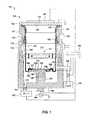
図1は、基板105を処理可能な処理キット150の一実施形態を有する例示的な半導体処理チャンバ100を示す。処理キット150は、一体型下方シールド160、介挿カバーリング170、堆積リング180及び中間シールド190を含む。図示の実施形態において、処理チャンバ100は、チタン、酸化アルミニウム、アルミニウム、銅、タンタル、窒化タンタル、タングステン又は窒化タングステンを基板上に堆積可能なスパッタリングチャンバ(物理気相蒸着又はPVDチャンバとも称される)を含む。適したPVDチャンバの例には、ALPS(商標名)PLus及びSIP ENCORE(商標名)PVD処理チャンバが含まれ、両方共、カリフォルニア州サンタクララのアプライドマテリアルズ社から商業的に入手可能である。その他の製造業者から入手可能な処理チャンバを利用して本明細書に記載の実施形態を実行することも考えられる。 FIG. 1 illustrates an exemplary
処理チャンバ100は、内部容積110又はプラズマ区域を取り囲む囲壁102及び側壁104を有するチャンバ本体部101、底壁106及び蓋アセンブリ108を含む。チャンバ本体部101は典型的にはステンレススチールの溶接板又はアルミニウムの単塊から作製される。側壁104は一般に、基板105を処理チャンバ100内外に搬入・搬出するためのスリットバルブ(図示せず)を有する。側壁104に配置されたポンピングポート120は、排気を行い内部容積110の圧力を制御するポンピングシステム122に連結される。処理チャンバ100の蓋アセンブリ108は、カバーリング170に介挿される下方シールド160、中間シールド190及び上方シールド195と協働して、内部容積110内で形成されたプラズマを基板の上の領域に閉じ込める。 The
台座アセンブリ124は、チャンバ100の底壁106によって支持される。台座アセンブリ124は、処理中、堆積リング180を基板105と共に支持する。台座アセンブリ124は、上方位置と下方位置との間で台座アセンブリ124を移動するように構成された昇降機構126によって、チャンバ100の底壁106に連結される。加えて、下方位置において、昇降ピンを台座アセンブリ124を貫通させて動かすことによって基板105を台座アセンブリ124から離し、処理チャンバ100外部に配置されたウェハ搬送機構(シングルブレードロボット等(図示せず))との間での基板105の受け渡しを円滑に行うことができる。蛇腹部129は典型的には台座アセンブリ124とチャンバ底壁106との間に配置され、チャンバ本体部101の内部容積110を台座アセンブリ124の内部及びチャンバ外部から隔離している。 The
台座アセンブリ124は一般に、プラットフォームハウジング130に封止連結された基板支持体128を含む。このプラットフォームハウジング130は典型的には、ステンレススチール、アルミニウム等の金属材料から作製される。一般には冷却プレート(図示せず)をプラットフォームハウジング130内に配置し、基板支持体128の温度調節を行う。本発明が有益となるように構成し得る台座アセンブリ124の1つが、1996年4月16日にDavenportらに発行された米国特許第5507499号に記載されており、この文献は参照により全て本明細書に組み込まれる。 The
基板支持体128は、アルミニウム又はセラミックを含むことができる。基板支持体128は、処理中、基板105を受け止めて支持する基板受け面132を有し、基板受け面132は、スパッタリングターゲット136のスパッタリング面134に実質的に平行な面を有する。支持体128は、基板105の張り出し縁部107の手前で終端する周壁138も有する。基板支持体128は、静電チャック、セラミック体、ヒータ又はこれらの組み合わせであってもよい。一実施形態において、基板支持体128は、導電層が埋設された誘電性本体部を含む静電チャックである。誘電性本体部は、典型的には高熱伝導性の誘電体(熱分解窒化ホウ素、窒化アルミニウム、窒化シリコン、アルミナ等)又は同等の材料から作製される。 The
蓋アセンブリ108は一般に、ターゲット136及びマグネトロン140を含む。蓋アセンブリ108は、図1に示されるように、閉鎖位置にある場合、側壁104によって支持される。アイソレータリング142がターゲット136と上方シールド195との間に配置され、その間での真空漏れを防止し且つチャンバ壁とターゲット136との間での電気的短絡を軽減する。一実施形態において、上方シールド195は、アルミニウム、ステンレススチール等の材料を含む。 The
ターゲット136は蓋アセンブリ108に連結され、処理チャンバ100の内部容積110に露出している。ターゲット136は、PVD処理中、基板上に堆積させる材料を提供する。アイソレータリング142を、ターゲット136とチャンバ本体部101との間に配置し、ターゲット136をチャンバ本体部101から絶縁する。一実施形態において、アイソレータリング142はセラミック材料を含む。 The
ターゲット136及び台座アセンブリ124は、電源144によって互いに相対的にバイアス印加される。アルゴン等のガスは、ガス供給源146から導管148を介して内部容積110に供給される。ガス供給源146は、アルゴン、キセノン等の非反応性ガスを含むことができ、この非反応性ガスは、ターゲット136に力強く衝突し、材料をターゲット136からスパッタ可能である。ガス供給源146は、スパッタリング材料と反応して基板上に層を形成可能な反応性ガス、例えば酸素含有ガス及び窒素含有ガスの1種以上を含むこともできる。使用済みの処理ガス及び副生成物は、ポンピングポート120を通してチャンバ100から排出される。ポンピングポート120は、使用済みの処理ガスを受け取ると、スロットルバルブを有する排気管121へとその使用済みのガスを流すことによってチャンバ100内のガス圧を制御する。排気管148はポンピングシステム122に接続される。典型的には、チャンバ100内のスパッタリングガスの圧力は、大気圧より低いレベル(真空環境、例えばガス圧1mTorr〜400mTorr等)に設定される。プラズマは、基板105とターゲット136との間でガスから形成される。プラズマ中のイオンはターゲット136に向かって加速し、ターゲット136から材料を叩き出す。この叩き出されたターゲット材料が、基板105上に堆積される。
マグネトロン140は、蓋アセンブリ108に処理チャンバ100の外側で連結される。マグネトロン140は、PVD処理中のターゲット136の均等な消費を促進する少なくとも1つの回転磁石アセンブリ(図示せず)を含む。利用し得るマグネトロンの1つが、1999年9月21日にOrらに発行された米国特許第5953827号に記載されており、この文献は参照により全て本明細書に組み込まれる。 The
チャンバ100は、チャンバ100の構成材を操作してチャンバ100内で基板を処理するための命令セットを有するプログラムコードを搭載したコントローラ196によって制御される。例えば、コントローラ196は、基板支持体128を操作するための基板位置決め命令セット、ガス流量制御バルブを操作してスパッタリングガスのチャンバ100への流量を設定するためのガス流量制御命令セット、スロットルバルブを操作してチャンバ100内の圧力を維持するためのガス圧制御命令セット、支持体128又は側壁104内の温度制御システム(図示せず)を基板又は側壁104の設定温度にそれぞれ制御するための温度制御命令セット及びチャンバ100内の処理を監視するための処理監視命令セットを含むプログラムコードを搭載可能である。 The
コリメータ197を下方シールド160に連結して接地する。一実施形態において、コリメータは金属リングであってもよく、また外方管状セクション及び少なくとも1つの内方同心管状セクション、例えば支材でつながれた3つの同心管状セクションを含む。 A
チャンバ100は、例えば構成材表面のスパッタリング堆積物を洗浄するために、侵食された構成材を交換又は修繕するために又はチャンバ100を別の処理用に適合させるためにチャンバ100から簡単に取り外し可能な様々な構成材を備えた処理キット150も備える。一実施形態において、処理キット150は、下方シールド160、中間シールド190及び基板105の張り出し縁部107の手前で終端する基板支持体128の周壁138周囲に配置するためのリングアセンブリ202を備える。図2に示されるように、リングアセンブリ202は、堆積リング180及びカバーリング170を備える。堆積リング180は、支持体128を取り囲む環状バンド402を備える。カバーリング170は少なくとも部分的に堆積リング180を覆う。堆積リング180とカバーリング170とが協働することによって、支持体128の周壁138及び基板105の張り出し縁部107上でのスパッタ堆積物の発生が減少する。 The
下方シールド160は、基板支持体128に面するスパッタリングターゲット136のスパッタリング面134及び基板支持体128の周壁138を取り囲む。下方シールド160は、チャンバ100の側壁104を覆って隠し、下方シールド160の背後の構成材及び表面上への、スパッタリングターゲット136のスパッタリング面134から発生するスパッタリング堆積物の堆積を軽減する。例えば、下方シールド160は、支持体128の表面、基板105の張り出し縁部107、チャンバ100の側壁104及び底壁106を保護可能である。 The
図3A及び3Bは、本明細書に記載の一実施形態による下方シールドの部分断面図である。図3Cは、図3Aの下方シールドの上面図である。図1及び図3A〜3Cに示されるように、下方シールド160は一体構成であり、スパッタリングターゲット136のスパッタリング面134及び基板支持体128を取り囲む寸法設計の直径を有する円筒状外方バンド310を備える。円筒状外方バンド310は、スパッタリングターゲット136のスパッタリング面134を取り囲む上部壁312を有する。支持棚部313は、円筒状外方バンド310の上部壁312から半径方向外側に延びる。支持棚部313は、チャンバ100の側壁104を取り囲む第1環状アダプタ172上に載置される載置面314を備える。載置面314は、下方シールド160を第1環状アダプタ172に整列させるためのピンを受けるような形状に形成された複数のスロットを有していてもよい。 3A and 3B are partial cross-sectional views of a lower shield according to one embodiment described herein. 3C is a top view of the lower shield of FIG. 3A. As shown in FIGS. 1 and 3A-3C, the
図3Bに示されるように、上部壁312は、内周部326及び外周部328を備える。外周部328は傾斜段差部330を形成するように延びる。傾斜段差部330は、垂直線から半径方向外側に約5°〜約10°、例えば垂直線から約8°傾斜している。一実施形態において、内周部326は、垂直線から半径方向内側に約2°〜約5°、例えば約3.5°傾斜している。 As shown in FIG. 3B, the
第1環状アダプタ172は下方シールド160を支持し、また基板処理チャンバ100の側壁104周囲での熱交換機として機能可能である。第1環状アダプタ172とシールド160とがアセンブリを構成することによってシールド160からアダプタ172へのより良好な熱伝達がなされ、シールド上に堆積された材料にかかる熱膨張応力が減少する。基板処理チャンバ内で形成されたプラズマへの曝露によってシールド160の一部が過剰に熱せられてシールドが熱膨張してしまい、その上のスパッタリング堆積物が剥落し、基板105上に落ちて基板を汚染する場合がある。第1アダプタ172は、下方シールド160の載置面314と接触する接触面174を有していることからシールド160とアダプタ172との間で良好な熱導電性が得られる。一実施形態において、シールド160の載置面314及び第1アダプタ172の接触面174はそれぞれ約10〜約80マイクロインチ又は約16〜約63マイクロインチもの表面粗さ又は、一実施形態において、平均表面粗さ約32マイクロインチを有する。一実施形態において、第1アダプタ172は、熱伝達流体を流して第1アダプタ172の温度を制御するための導管を更に備える。 The first
下方シールド160の支持棚部313の下には、基板支持体128を取り囲む底部壁316がある。ベースプレート318が円筒状外方バンド310の底部壁316から半径方向内側に延びる。円筒状内方バンド320はベースプレート318に連結され、少なくとも部分的に基板支持体128の周壁138を取り囲む。円筒状内方バンド320、ベースプレート318及び円筒状外方バンド310はU型チャネルを構成する。円筒状内方バンド320は、円筒状外方バンド310の高さより低い高さを有する。一実施形態において、内方バンド320の高さは、円筒状外方バンド310の高さの約5分の1である。一実施形態において、底部壁316はノッチ322を有する。一実施形態において、円筒状外方バンド310は一連のガス穴部324を有する。 Below the
円筒状外方バンド310、上部壁312、支持棚部313、底部壁316及び内方円筒状バンド320は一体構造をなす。例えば、一実施形態においては下方シールド160全体を300シリーズのステンレススチールから、別の実施形態においてはアルミニウムから形成可能である。一体型下方シールド160は、複数の構成材、多くは2つか3つの別々の部品で完全な下方シールドを構成する従来のシールドより有利である。例えば、単一部品のシールドのほうが、複数の部品から成るシールドより熱処理及び冷却処理の両方において熱的に均一である。例えば、単一部品の下方シールド160は第1アダプタ172に対して1つしか熱界面を有していないため、シールド160と第1アダプタ172との間での熱交換をより制御しやすくなる。複数の構成材から成るシールド160だと、クリーニングの際にシールドを取り外すのがより困難で手間がかかってしまう。単一部品のシールド160のスパッタリング堆積物に曝される面は連続的であり、洗浄がより困難となる界面や角がない。また、この単一部品のシールド160は、処理サイクル中、側壁104をスパッタ堆積からより効果的に遮断する。 The cylindrical
一実施形態においては、下方シールド160の露出面を、カリフォルニア州サンタクララのアプライドマテリアルズ社から商業的に入手可能なCLEANCOAT(商標名)で処理する。CLEANCOAT(商標名)はツインワイヤアルミニウムアーク溶射コーティングであり、基板処理チャンバ構成材(下方シールド160等)に適用することによって下方シールド160上への堆積物の粒子落下を軽減してチャンバ100内の基板105の汚染を防止する。一実施形態において、下方シールド160上のツインワイヤアルミニウムアーク溶射コーティングは、約600〜約2300マイクロインチの表面粗さを有する。 In one embodiment, the exposed surface of
下方シールド160は、チャンバ100内の内部容積110に面した露出面を有する。一実施形態においては、露出面にビードブラスト加工を施して表面粗さを175±75マイクロメートルとする。テクスチャ加工されたビードブラスト加工済み表面は、粒子の落下を軽減し、またチャンバ100内の汚染を防止する役割を果たす。平均表面粗さは、露出面に沿った粗さを特徴づける山及び谷の平均線からの差の絶対値の平均である。平均粗さ、ひずみ又はその他の特性は、露出面に針を通して表面上の凸凹の高さの変動のトレースを描く粗面計又は表面で反射した電子ビームを利用して表面の画像を得る走査電子顕微鏡によって求めることができる。 The
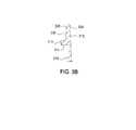
図4A〜4Cを参照するが、堆積リング180は図2に示されるように支持体128の周壁138近くまで延びそれを取り囲む環状バンド402を備える。環状バンド402は、バンド402から横方向に延び且つ支持体128の周壁138と実質的に平行な内方リップ部404を備える。内方リップ部404は、基板105の張り出し縁部107のすぐ下で終端する。内方リップ部404は、基板105の周縁部及び基板支持体128を取り囲む堆積リング180の内周を定め、処理中、基板105によって覆われない支持体128の領域を保護する。例えば、内方リップ部404は、そのままでは処理環境に露出してしまう支持体128の周壁138を取り囲み且つ少なくとも部分的に覆うことによって、周壁138上へのスパッタリング堆積物の堆積を軽減する又は完全に妨げさえする。有利には、堆積リング180を簡単に取り外してリング180の露出面からスパッタリング堆積物を洗浄することが可能であり、支持体128を洗浄のために分解する必要がない。堆積リング180は、支持体128の露出側面を保護して、エネルギー印加されたプラズマ種によるその侵食を軽減する役目を果たすことも可能である。 Referring to FIGS. 4A-4C, the
図2に示す実施形態において、堆積リング180の環状バンド402は、バンド402の中央部位に沿って延びるV型突起部406を有し、このV型突起部406の両側には第1半径方向内側凹部408a及び第2半径方向内側凹部408bがある。一実施形態において、V型突起部406の対向する面は角度αを形成する。一実施形態において、この角度αは約25°〜約30°である。別の実施形態において、角度αは約27°〜約28°である。第1半径方向内側凹部408aは、第2半径方向内側凹部408bの水平面より若干下の水平面に位置する。一実施形態において、第2半径方向内側凹部408bは、約0.8インチ〜約0.9インチの幅を有する。別の実施形態において、第2半径方向内側凹部408bは、約0.83インチ〜約0.84インチの幅を有する。一実施形態において、第1半径方向内側凹部408a及び第2半径方向内側凹部408bは、堆積リング180の底面420と実質的に平行である。第2半径方向内側凹部408bはカバーリング170から離間され、カバーリング170との間にアーク状チャネル410を形成し、このアーク状チャネルは、図2に示されるように、プラズマ種のアーク状チャネル410内への侵入を軽減するための迷路として機能する。開放内方チャネル412は内方リップ部404とV型突起部406との間に延びる。開放内方チャネル412は半径方向内側に延び、基板105の張り出し縁部107の少なくとも部分的に下で終端する。開放内方チャネル412によって、堆積リング180の洗浄中のこれらの部位からのスパッタリング堆積物の除去が円滑になる。堆積リング180は、外側に延び且つV型突起部406の半径方向外側に位置する棚部414も有する。棚部414はカバーリング170を支持する役割を果たす。環状バンド402の底面420は、V型突起部406下を内方リップ部404から延びるノッチ422を有する。一実施形態において、このノッチは約0.6インチ〜約0.75インチの幅を有する。別の実施形態において、ノッチは約0.65インチ〜約0.69インチの幅を有する。一実施形態において、ノッチは約0.020インチ〜約0.030インチの高さを有する。別の実施形態において、ノッチは約0.023インチ〜約0.026インチの高さを有する。 In the embodiment shown in FIG. 2, the
一実施形態において、第2半径方向内側凹部408bは、矢印Aで示される外径を有する。一実施形態において、第2半径方向内側凹部408bの直径Aは約13インチ〜約13.5インチである。別の実施形態において、第2半径方向内側凹部408bの直径Aは、約13.1インチ〜約13.2インチである。一実施形態において、第2半径方向内側凹部408bは、矢印Eで示される内径を有する。一実施形態において、第2半径方向内側凹部408bの直径Eは約12インチ〜約12.5インチである。別の実施形態において、直径Eは約12.2インチ〜約12.3インチである。 In one embodiment, the second radially
一実施形態において、環状バンド402は、矢印Dで示されるような直径を有する。一実施形態において、環状バンド402の直径Dは約11インチ〜約12インチである。別の実施形態において、環状バンド402の直径Dは約11.25インチ〜約11.75インチである。更に別の実施形態において、環状バンド402の直径Dは約11.40インチ〜約11.60インチである。一実施形態において、環状バンド402は、矢印Fによって示されるような外径を有する。一実施形態において、環状バンド402の直径Fは約13インチ〜約14インチである。別の実施形態において、環状バンド402の直径Fは約13.25インチ〜約13.75インチである。更に別の実施形態において、直径Fは13.40インチ〜約13.60インチである。 In one embodiment, the
一実施形態において、V型突起部の上部は、矢印Bによって示される直径を有する。一実施形態において、直径Bは約12インチ〜約12.3インチである。別の実施形態において、直径Bは約12.1インチ〜約12.2インチである。 In one embodiment, the top of the V-shaped protrusion has a diameter indicated by arrow B. In one embodiment, the diameter B is about 12 inches to about 12.3 inches. In another embodiment, the diameter B is about 12.1 inches to about 12.2 inches.
一実施形態において、内方リップ部404は、矢印Cによって示される外径を有する。一実施形態において、直径Cは約11インチ〜約12インチである。別の実施形態において、直径Cは約11.5インチ〜約11.9インチである。更に別の実施形態において、直径Cは約11.7インチ〜約11.8インチである。 In one embodiment, the
堆積リング180は、セラミック材料(酸化アルミニウム等)を成形し機械加工することによって作製可能である。好ましくは、酸化アルミニウムは、望ましくない元素(鉄等)によるチャンバ100の汚染を軽減するために少なくとも約99.5%の純度を有する。このセラミック材料を、慣用の技法(静水圧プレス成形等)用いて成型及び焼成し、それに続いて適切な機械加工法を用いて成型・焼成された予備成形物を機械加工することで必要とされる形状と寸法にする。 The
堆積リング180の環状バンド402は、グリットブラスト加工された露出面を含むことができる。グリットブラスト加工は、既定の表面粗さを得るのに適したグリットサイズで行われる。一実施形態においては、堆積リング180の表面をツインワイヤアルミニウムアーク溶射コーティング(例えば、CLEANCOAT(商標名)等)で処理して、粒子の落下と汚染を軽減する。 The
図5Aは、本明細書に記載の一実施形態による中間シールド190の部分断面図である。中間シールド190は、基板支持体128に面したスパッタリングターゲット136のスパッタリング面134を取り囲む。中間シールド190は下方シールド160の上部壁312及びチャンバ100の側壁104を覆って隠し、中間シールド160の背後の構成材及び表面上への、スパッタリングターゲット136のスパッタリング面134から発生するスパッタリング堆積物の堆積を軽減する。 FIG. 5A is a partial cross-sectional view of an
図1及び5Aに示されるように、中間シールド160は一体構成であり、上方シールド195を取り囲む寸法設計の第1直径D1を有する円筒状バンド510を備える。円筒状外方バンド310は、上方シールド195を取り囲む上部壁512、中間壁517及び底部壁518を有する。取付フランジ514が円筒状バンド510の上部壁512から半径方向外側に延びる。取付フランジ514は、チャンバ100の側壁104を取り囲む第2環状アダプタ176上に載置される載置面516を備える。載置面は、中間シールド190をアダプタ176に整列させるためのピンを受けるような形状に形成された複数のスロットを備えていてもよい。 As shown in FIGS. 1 and 5A, the
中間壁517は上部壁512の延長である。中間壁517は、上部壁512から、上部壁512と中間壁517との間の移行点から始まって半径方向内側に傾斜している。一実施形態において、中間壁517は垂直線から約5°〜約10°、例えば垂直線から約7°傾斜している。円筒状バンドの中間壁517は第2直径D2を形成する。第2直径D2は、下方シールド160の上部壁312の傾斜部位内に収まるように寸法設計される。 The
底部壁518は、中間壁517の延長である。底部壁518は、中間壁517と底部壁518との間の移行点から始まって中間壁517に対して半径方向外側に傾斜している。一実施形態において、底部壁518は垂直線から約1°〜約5°、例えば垂直線から約4°傾斜している。 The
上部壁512、中間壁517、底部壁518及び取付フランジ514は一体構造をなす。例えば、一実施形態において、中間シールド190全体を300シリーズのステンレススチールから、別の実施形態においてはアルミニウムから作製可能である。 The
図1、2、6A、6B、6Cを参照するが、カバーリング170は、堆積リング180を取り囲み且つ少なくとも部分的に覆うことによってスパッタリング堆積物の大部分を受け止め、堆積リング180を堆積物から守っている。カバーリング170は、スパッタリングプラズマによる侵食に耐性がある材料、例えば金属材料(ステンレススチール、チタン、アルミニウム等)又はセラミック材料(酸化アルミニウム等)から作製される。一実施形態において、カバーリング170は、少なくとも約99.9%の純度を有するチタンから構成される。一実施形態においては、カバーリング170の表面をツインワイヤアーク溶射コーティング(例えば、CLEANCOTA(商標名)等)で処理することによって、カバーリング170の表面からの粒子落下を軽減する。カバーリングは、矢印Hによって示される外径を有する。一実施形態において、直径Hは約14.5インチ〜約15インチである。別の実施形態において、直径Hは約14.8インチ〜約14.9インチである。カバーリングは、矢印Iによって示される内径を有する。一実施形態において、直径Iは約11.5インチ〜約12.5インチである。別の実施形態において、直径Iは約11.8インチ〜約12.2インチである。更に別の実施形態において、直径Iは約11.9インチ〜約12.0インチである。 Referring to FIGS. 1, 2, 6A, 6B, and 6C, the
カバーリング170は、環状ウェッジ602を備える。この環状ウェッジは、上面603及び堆積リング180の棚部414上に載置される底面604を備える。上面603は実質的に底面604に平行である。傾斜上面603は上面603と突出ブリム610とを連結している。傾斜上面605は半径方向内側に傾斜し且つ基板支持体128を取り囲む。環状ウェッジ602の傾斜上面605は内周部及び外周部606、608を有する。内周部606は突出ブリム610を含み、この突出ブリムは堆積リング180の第2半径方向内側凹部408b上にかかり、堆積リング180のアーク状チャネル410を形成している。突出ブリム610によって、堆積リング180のアーク状チャネル410上へのスパッタリング堆積物の堆積が減少する。有利には、突出ブリム610は、堆積リング180と共に形成される開放内方チャネル412の幅の少なくとも約半分に対応する距離だけ突出する。突出ブリム610はアーチ状チャネル410及び開放内方チャネル412と協働し且つ相補することによってカバーリング170と堆積リング180との間に回旋状の狭窄した流路を形成するようなサイズ、形状及び位置に構成され、この流路が周壁138上への処理堆積物の流れを阻害する。アーク状チャネル410の狭窄した流路により、そのままでは互いに膠着する又は基板105の外縁の張り出し縁部と膠着してしまう、堆積リング180とカバーリング170との係合面上での低エネルギースパッタ堆積物の増加が制限される。基板105の張り出し縁部107の下に延びる堆積リング180の開放内方チャネル412は、カバーリング170の突出ブリム610による保護と共に、例えば、アルミニウムスパッタリングチャンバにおいてアルミニウムスパッタ堆積物を回収し、その一方で2つのリング170、180の係合面上へのスパッタ堆積を軽減する又は実質的に妨げるように設計されている。 The
傾斜上面605は、突出ブリム610と協働して視線方向の堆積物が内部容積110から流出してチャンバ本体キャビティへと侵入するのを阻止する。傾斜上面605を、角度βで示されるように、上面603に対してある角度でもって傾斜させることができる。一実施形態において、角度βは約5°〜約15°である。別の実施形態において、角度βは約9°〜約11°である。一実施形態において、角度βは約10°である。カバーリング170の傾斜上面605の角度は、例えば、基板105の張り出し縁部107に最も近い位置での、そのままでは基板105全体で得られる堆積の均一性に悪影響を与えてしまうスパッタ堆積物の増加を最小限に留めるように設計されている。 The inclined
カバーリング170は、環状ウェッジ602の傾斜上面605下に位置する傾斜段差部612を更に備える。この傾斜段差部612は、突出ブリム610と底面604とを連結している。傾斜段差部612は環状ウェッジ602から下方向に且つ内周部606から半径方向外側に延びる。傾斜段差部612は、角度Yに示されるように底面に対してある角度で傾斜させることができる。一実施形態において、角度Yは約40°〜約50°である。別の実施形態において、角度Yは約42°〜約48°である。更に別の実施形態において、角度Yは約44°〜約46°である。 The
傾斜段差部は、矢印Jによって示される内径を有する。一実施形態において、傾斜段差部612の直径Jは約12インチ〜約13インチである。別の実施形態において、傾斜段差部612の直径Jは約12.2インチ〜約12.5インチである。更に別の実施形態において、傾斜段差部612の直径Jは約12.3インチ〜約12.4インチである。傾斜段差部612は、矢印Kによって示される直径も有する。一実施形態において、傾斜段差部612の直径Kは約12.5インチ〜約13インチである。別の実施形態において、傾斜段差部612の直径Kは約12.7インチ〜約12.8インチである。一実施形態において、傾斜段差部612の直径Kは、底面604の内径として機能する。 The inclined step portion has an inner diameter indicated by an arrow J. In one embodiment, the
底面は、矢印Lによって示される外径を有する。一実施形態において、底面の直径Lは約13.5インチ〜約13.8インチである。別の実施形態において、直径Lは約13.4インチ〜約13.5インチである。 The bottom surface has an outer diameter indicated by an arrow L. In one embodiment, the bottom surface diameter L is between about 13.5 inches and about 13.8 inches. In another embodiment, the diameter L is between about 13.4 inches and about 13.5 inches.
カバーリング170は、環状ウェッジ602から下方向に延びる内方円筒状バンド614a及び外方円筒状バンド614bを更に備え、これらの間に間隙616を有する。一実施形態において、間隙616は幅0.5インチ〜約1インチを有する。別の実施形態において、間隙616は幅約0.7インチ〜約0.8インチを有する。一実施形態において、内方及び外方円筒状バンド614a、614bは実質的に垂直である。円筒状バンド614a、614bは、ウェッジ602の傾斜段差部602の半径方向外側に位置する。内方円筒状バンド614aの内周部618は、底面604に連結される。一実施形態において、内方円筒状バンド614aの内周部618は、垂直線から角度Φで傾斜している。一実施形態において、角度Φは約10°〜約20°である。別の実施形態において、角度Φは約14°〜約16°である。 The
内方円筒状バンド614aは、外方円筒状バンド614bより低い高さを有する。典型的には、外方円筒状バンド614bの高さは、内方円筒状バンド614aの高さの少なくとも約2倍である。一実施形態において、外方円筒状バンド614bの高さは約0.4インチ〜約1インチである。別の実施形態において、外方円筒状バンド614bの高さは0.6インチ〜0.7インチである。一実施形態において、内方円筒状バンド614aの高さは約0.2インチ〜0.6インチである。別の実施形態において、内方円筒状バンド614aの高さは約0.3インチ〜0.4インチである。 The inner
一実施形態において、底面の外径Lは、内方円筒状バンド614aの内径として機能する。内方円筒状バンド614aは、矢印Mによって示される外径を有する。一実施形態において、内方円筒状バンド614aの直径Mは約13.5インチ〜約14.2インチである。別の実施形態において、内方円筒状バンド614aの直径Mは約13.7〜14インチである。更に別の実施形態において、内方円筒状バンドの直径Mは約13.8インチ〜約13.9インチである。 In one embodiment, the outer diameter L of the bottom surface functions as the inner diameter of the inner
一実施形態において、外方円筒状バンド614bは、矢印Nによって示されるような内径を有する。一実施形態において、直径Nは約14インチ〜約15インチである。別の実施形態において、外方円筒状バンド614bの直径Nは約14.2インチ〜約14.8インチである。別の実施形態において、外方円筒状バンド614bの直径Nは約14.5インチ〜約14.6インチである。一実施形態において、カバーリングの直径Hは、外方円筒状バンドHの外径として機能する。 In one embodiment, the outer
一実施形態において、カバーリング170は異なる高さ範囲で調節可能であり且つ下方シールド160のコンダクタンス穴部を効果的に遮蔽する。例えば、カバーリング170を上昇又は下降させてチャンバ100内での基板支持体128に対してのその高さを調節することが可能である。 In one embodiment, the
下方シールド160とカバーリング170との間の空間又は間隙が、プラズマが通る回旋状のS型経路又は迷路を形成する。この経路の形状は、例えば、プラズマ種のこの領域への侵入を妨害し且つ遅らせることによってスパッタ材料の望ましくない堆積を軽減することから有利である。 The space or gap between the
上記は本発明の実施形態を対象としているが、本発明の基本的な範囲から逸脱することなく本発明のその他及び更に別の実施形態を創作することができ、本発明の範囲は以下の特許請求の範囲に基づいて定められる。 While the above is directed to embodiments of the invention, other and further embodiments of the invention may be made without departing from the basic scope of the invention and the scope of the invention is subject to the following patents: It is determined based on the scope of claims.
Claims (15)
Translated fromJapanese基板処理チャンバは、第1環状アダプタと、基板処理チャンバにおいて基板支持体の周壁を取り囲むための堆積リングと、基板処理チャンバにおいて堆積リングを取り囲み且つ堆積リングをスパッタリング堆積物から少なくとも部分的に守るためのカバーリングとを含み、
堆積リングは、
基板支持体の周壁を取り囲むための環状バンドであって、環状バンドが、
環状バンドから横方向に延び且つ基板支持体の周壁と実質的に平行である内方リップ部を備え、内方リップ部が、基板の周縁部及び基板支持体を取り囲む堆積リングの内周を定め、処理中、基板によって覆われない基板支持体の領域を保護して周壁上へのスパッタリング堆積物の堆積を軽減する又は完全に防止する環状バンドと、
ある角度を形成する対向する面を備えた単一のV型突起部であって、V型突起部は、バンドの中央部位に沿って延び、V型突起部は、V型突起部の内方リップ部に隣接した第1半径方向内側凹部及び半径方向外側にある第2半径方向内側凹部を有し、第1及び第2半径方向内側凹部は、互いに同心であり、第1半径方向内側凹部は、第2半径方向内側凹部の水平面の下方の水平面内に位置し、第1及び第2半径方向内側凹部は、実質的に平面であり、第2半径方向内側凹部は、カバーリングと共にアーク状チャネルを形成するように構成された単一のV型突起部を有する環状バンドと、
棚部の端部でカバーリングを支持するために構成された、V型突起部から外側に延びる棚部を含み、
カバーリングは、
環状ウェッジを備え、環状ウェッジが、
上面と、
基板支持体を取り囲むための傾斜上面であって、傾斜上面は、半径方向内側に傾斜し且つ内周部を有し、傾斜上面は、外周部を有する上面に連結された傾斜上面と、
堆積リングのV型突起部から外側へ延びる棚部の端部に載置されるように構成される底面とを備え、上面が実質的に底面に平行であり、
環状ウェッジが更に、
傾斜上面によって上面に連結された突出ブリムを備え、傾斜上面が突出ブリムと協働して直進方向の堆積物が内部容積から流出してチャンバ本体キャビティへと侵入するのを阻止し、
環状ウェッジが更に、
環状ウェッジの傾斜上面下に位置し且つ突出ブリムを底面と連結している傾斜段差部を備え、傾斜段差部は、堆積リングと共に空間を形成し、底面は、堆積リングと共に前記空間よりも狭いアーク状チャネルを形成するように構成され、
カバーリングが更に、
環状ウェッジから下方向に延びる円筒状内方バンド及び円筒状外方バンドを備え、円筒状内方バンドが円筒状外方バンドより低い高さを有し、
下方シールドは、
スパッタリングターゲットのスパッタリング面及び基板支持体を取り囲む寸法設計の第1直径を有する円筒状外方バンドを備え、円筒状外方バンドは、
複数のガス穴部と、
基板支持体を取り囲むように構成された底部壁と、
スパッタリングターゲットのスパッタリング面を取り囲むように構成された上部壁とを備え、上部壁は、
内部に面し、底部壁へ向かって垂直線から半径方向内側に傾斜する内周部と、
外側に面する外周部であって、外周部は傾斜段差部を形成するように延び、傾斜段差部が垂直線から半径方向外側に傾斜し且つ底部壁から離れている外周部とを備え、
下方シールドが更に、
第1環状アダプタの接触面と接触して熱界面を形成するように構成された載置面を備え且つ円筒状外方バンドから半径方向外側に延びる支持棚部であって、載置面は約10〜約80マイクロインチの表面粗さを有し且つ下方シールドを整列させるためのピンを受けるような形状に形成された複数のスロットを有する支持棚部と、
円筒状外方バンドの底部壁から半径方向内側に延びるベースプレートと、
ベースプレートに連結され且つ基板支持体の周縁部を部分的に取り囲むように構成された円筒状内方バンドとを備える下方シールド。A lower shield for enclosing the sputtering target and the substrate supportwithin the inner volume of the substrate processing chamber,
The substrate processing chamber includes a first annular adapter, a deposition ring for surrounding the peripheral wall of the substrate support in the substrate processing chamber, and surrounding the deposition ring in the substrate processing chamber and at least partially protecting the deposition ring from sputtering deposits. Including the cover ring,
The deposition ring
An annular band for surrounding the peripheral wall of the substrate support, the annular band,
An inner lip extending laterally from the annular band and substantially parallel to the peripheral wall of the substrate support, the inner lip defining the peripheral edge of the substrate and the inner periphery of the deposition ring surrounding the substrate support An annular band that protects the area of the substrate support that is not covered by the substrate during processing to reduce or completely prevent the deposition of sputtering deposits on the peripheral wall;
A single V-shaped protrusion with opposing faces forming an angle, the V-shaped protrusion extending along the central portion of the band, and the V-shaped protrusion being inward of the V-shaped protrusion A first radially inner recess adjacent to the lip and a second radially inner recess located radially outward, wherein the first and second radially inner recesses are concentric with each other, and the first radially inner recess is , Located in a horizontal plane below the horizontal plane of the second radially inner recess, the first and second radially inner recesses are substantially planar, and the second radially inner recess is an arcuate channel with the cover ring An annular band having a single V-shaped projection configured to form
Configured to support the cover ring at the end of the shelf, including a shelf extending outward from the V-shaped protrusion,
Covering
With an annular wedge,
The top surface;
An inclined upper surface for surrounding the substrate support, the inclined upper surface being inclined radially inward and having an inner peripheral portion, the inclined upper surface being connected to the upper surface having the outer peripheral portion;
A bottom surface configured to be placed on an end of a shelf extending outwardly from the V-shaped protrusion of the deposition ring, the top surface being substantially parallel to the bottom surface,
An annular wedge
A protruding brim connected to the upper surface by an inclined upper surface, the inclined upper surface cooperating with the protruding brim to prevent sediment in a straight direction from flowing out of the internal volume and entering the chamber body cavity;
An annular wedge
An inclined step portion is provided below the inclined upper surface of the annular wedge and connects the protruding brim to the bottom surface. The inclined step portion forms a space together with the deposition ring, and the bottom surface forms an arc narrower than the space together with the deposition ring. Configured to form a channel-like channel,
The cover ring
A cylindrical inner band and a cylindrical outer band extending downward from the annular wedge, the cylindrical inner band having a lower height than the cylindrical outer band;
The lower shield
Comprises a cylindrical outer band having a first diameter dimensioned to encircle the sputtering surface and the substrate support of the sputtering target, the cylindricalouter band,
A plurality of gas holes,
A bottom wall configured to surround the substrate support;
An upper wall configured to surround the sputtering surface of the sputtering target,
An inner periphery facing inward and inclined radially inward from a vertical line toward the bottom wall;
An outer peripheral portion facingoutward , the outer peripheral portion extending so as to form an inclined stepped portion, the inclined stepped portion being inclined radially outward from the vertical line and being separated from the bottom wall,
The lower shield further
A support shelf havinga mounting surfaceconfigured to contact the contact surface of the first annular adapter to form a thermal interface and extending radially outward from the cylindrical outer band, the mounting surface being approximately A support shelf having a plurality of slots having a surface roughness of 10 to about 80 microinches and shaped to receive pins for aligning the lower shield ;
A base plate extending radially inward from the bottom wall of the cylindricalouter band;
A lower shield comprising a cylindrical inner band coupled to the base plate and configured to partially surround the periphery of the substrate support.
円筒状内方バンドが、円筒状外方バンドの高さより低い高さを有する、請求項1記載の下方シールド。A cylindrical inner band, a base plate, anda cylindrical outer band form a U-shaped channel,
The lower shield of claim 1, wherein the cylindrical inner band has a height that is less than a height of the cylindrical outer band.
基板処理チャンバは、第1環状アダプタと、基板処理チャンバの内側容積内においてスパッタリングターゲット及び基板支持体を取り囲むための下方シールドと、基板処理チャンバにおいて堆積リングを取り囲み且つ堆積リングをスパッタリング堆積物から少なくとも部分的に守るためのカバーリングとを含み、
下方シールドは、
スパッタリングターゲットのスパッタリング面及び基板支持体を取り囲む寸法設計の第1直径を有する円筒状外方バンドを備え、円筒状外方バンドは、
複数のガス穴部と、
基板支持体を取り囲むように構成された底部壁と、
スパッタリングターゲットのスパッタリング面を取り囲むように構成された上部壁とを備え、上部壁は、
内部に面し、底部壁へ向かって垂直線から半径方向内側に傾斜する内周部と、
外側に面する外周部であって、外周部は傾斜段差部を形成するように延び、傾斜段差部が垂直線から半径方向外側に傾斜し且つ底部壁から離れている外周部とを備え、
下方シールドが更に、
第1環状アダプタの接触面と接触して熱界面を形成するように構成された載置面を備え且つ円筒状外方バンドから半径方向外側に延びる支持棚部であって、載置面は約10〜約80マイクロインチの表面粗さを有し且つ下方シールドを整列させるためのピンを受けるような形状に形成された複数のスロットを有する支持棚部と、
円筒状外方バンドの底部壁から半径方向内側に延びるベースプレートと、
ベースプレートに連結され且つ基板支持体の周縁部を部分的に取り囲むように構成された円筒状内方バンドとを備え、
カバーリングは、
環状ウェッジを備え、環状ウェッジが、
上面と、
基板支持体を取り囲むための傾斜上面であって、傾斜上面は、半径方向内側に傾斜し且つ内周部を有し、傾斜上面は、外周部を有する上面に連結された傾斜上面と、
堆積リングのV型突起部から外側へ延びる棚部の端部に載置されるように構成される底面とを備え、上面が実質的に底面に平行であり、
環状ウェッジが更に、
傾斜上面によって上面に連結された突出ブリムを備え、傾斜上面が突出ブリムと協働して直進方向の堆積物が内部容積から流出してチャンバ本体キャビティへと侵入するのを阻止し、
環状ウェッジが更に、
環状ウェッジの傾斜上面下に位置し且つ突出ブリムを底面と連結している傾斜段差部を備え、傾斜段差部は、堆積リングと共に空間を形成し、底面は、堆積リングと共に前記空間よりも狭いアーク状チャネルを形成するように構成され、
カバーリングが更に、
環状ウェッジから下方向に延びる円筒状内方バンド及び外方円筒状バンドを備え、円筒状内方バンドが外方円筒状バンドより低い高さを有し、
堆積リングは、
基板支持体の周壁を取り囲むための環状バンドであって、環状バンドが、環状バンドから横方向に延び且つ基板支持体の周壁と実質的に平行である内方リップ部を備え、内方リップ部が、基板の周縁部及び基板支持体を取り囲む堆積リングの内周を定め、処理中、基板によって覆われない基板支持体の領域を保護して周壁上へのスパッタリング堆積物の堆積を軽減する又は完全に防止する環状バンドと、
ある角度を形成する対向する面を備えた単一のV型突起部であって、V型突起部は、バンドの中央部位に沿って延び、V型突起部は、V型突起部の内方リップ部に隣接した第1半径方向内側凹部及び半径方向外側にある第2半径方向内側凹部を有し、第1及び第2半径方向内側凹部は、互いに同心であり、第1半径方向内側凹部は、第2半径方向内側凹部の水平面の下方の水平面内に位置し、第1及び第2半径方向内側凹部は、実質的に平面であり、第2半径方向内側凹部は、カバーリングと共にアーク状チャネルを形成するように構成された単一のV型突起部と、
棚部の端部でカバーリングを支持するために構成された、V型突起部から外側に延びる棚部を含む堆積リング。A deposition ring for surrounding a peripheral wall of a substrate support in asubstrate processing chamber,
The substrate processing chamber includes a first annular adapter, a lower shield for surrounding the sputtering target and the substrate support within the inner volume of the substrate processing chamber, and surrounding the deposition ring in the substrate processing chamber and removing the deposition ring from the sputtering deposit. Including a cover ring for partial protection,
The lower shield
A cylindrical outer band having a first dimension of a dimensional design surrounding the sputtering surface of the sputtering target and the substrate support,
A plurality of gas holes,
A bottom wall configured to surround the substrate support;
An upper wall configured to surround the sputtering surface of the sputtering target,
An inner periphery facing inward and inclined radially inward from a vertical line toward the bottom wall;
An outer peripheral portion facing outward, the outer peripheral portion extending so as to form an inclined stepped portion, the inclined stepped portion being inclined radially outward from the vertical line and being separated from the bottom wall,
The lower shield further
A support shelf having a mounting surface configured to contact the contact surface of the first annular adapter to form a thermal interface and extending radially outward from the cylindrical outer band, the mounting surface being approximately A support shelf having a plurality of slots having a surface roughness of 10 to about 80 microinches and shaped to receive pins for aligning the lower shield;
A base plate extending radially inward from the bottom wall of the cylindrical outer band;
A cylindrical inner band coupled to the base plate and configured to partially surround the periphery of the substrate support;
Covering
With an annular wedge,
The top surface;
An inclined upper surface for surrounding the substrate support, the inclined upper surface being inclined radially inward and having an inner peripheral portion, the inclined upper surface being connected to the upper surface having the outer peripheral portion;
A bottom surface configured to be placed on an end of a shelf extending outwardly from the V-shaped protrusion of the deposition ring, the top surface being substantially parallel to the bottom surface,
An annular wedge
A protruding brim connected to the upper surface by an inclined upper surface, the inclined upper surface cooperating with the protruding brim to prevent sediment in a straight direction from flowing out of the internal volume and entering the chamber body cavity;
An annular wedge
An inclined step portion is provided below the inclined upper surface of the annular wedge and connects the protruding brim to the bottom surface. The inclined step portion forms a space together with the deposition ring, and the bottom surface forms an arc narrower than the space together with the deposition ring. Configured to form a channel-like channel,
The cover ring
A cylindrical inner band and an outer cylindrical band extending downward from the annular wedge, the cylindrical inner band having a lower height than the outer cylindrical band;
The deposition ring
An annular band for surrounding the peripheral wall of the substrate support, the annular band is provided with a peripheral wall and substantially inward lip portions are parallel and the substrate support extends transversely from the annular band, the inner lip portion Defines the perimeter of the substrate and the inner periphery of the deposition ring surrounding thesubstrate support, and protects areas of thesubstrate support that are not covered by the substrate during processing to reduce the deposition of sputtering deposits on the peripheral wall, orAn annular band that completely prevents,
A single V-shaped protrusion with opposing faces forming an angle, the V-shaped protrusion extending along the centralportion of the band, and the V-shaped protrusion being inward of the V-shaped protrusion A first radially inner recess adjacent to the lip and a second radially inner recess located radially outward, wherein the first and second radially inner recesses are concentric with each other, and the first radially inner recess is , located in a horizontal plane below the horizontal plane of the second radially inward recess, first and second radially inward recess,Ri substantially planarder, second radially inner recess is arched with a covering A single V-shaped projection configured to form a channel;
A deposition ringincluding a shelf extending outwardly from the V-shaped protrusion, configured to support the cover ring at an end of the shelf .
基板処理チャンバは、第1環状アダプタと、基板処理チャンバの内側容積内においてスパッタリングターゲット及び基板支持体を取り囲むための下方シールドと、基板処理チャンバにおいて基板支持体の周壁を取り囲むための堆積リングとを含み、
下方シールドは、
スパッタリングターゲットのスパッタリング面及び基板支持体を取り囲む寸法設計の第1直径を有する円筒状外方バンドを備え、円筒状外方バンドは、
複数のガス穴部と、
基板支持体を取り囲むように構成された底部壁と、
スパッタリングターゲットのスパッタリング面を取り囲むように構成された上部壁とを備え、上部壁は、
内部に面し、底部壁へ向かって垂直線から半径方向内側に傾斜する内周部と、
外側に面する外周部であって、外周部は傾斜段差部を形成するように延び、傾斜段差部が垂直線から半径方向外側に傾斜し且つ底部壁から離れている外周部とを備え、
下方シールドが更に、
第1環状アダプタの接触面と接触して熱界面を形成するように構成された載置面を備え且つ円筒状外方バンドから半径方向外側に延びる支持棚部であって、載置面は約10〜約80マイクロインチの表面粗さを有し且つ下方シールドを整列させるためのピンを受けるような形状に形成された複数のスロットを有する支持棚部と、
円筒状外方バンドの底部壁から半径方向内側に延びるベースプレートと、
ベースプレートに連結され且つ基板支持体の周縁部を部分的に取り囲むように構成された円筒状内方バンドとを備え、
堆積リングは、
基板支持体の周壁を取り囲むための環状バンドであって、環状バンドが、環状バンドから横方向に延び且つ基板支持体の周壁と実質的に平行である内方リップ部を備え、内方リップ部が、基板の周縁部及び基板支持体を取り囲む堆積リングの内周を定め、処理中、基板によって覆われない基板支持体の領域を保護して周壁上へのスパッタリング堆積物の堆積を軽減する又は完全に防止する環状バンドと、
ある角度を形成する対向する面を備えた単一のV型突起部であって、V型突起部は、バンドの中央部位に沿って延び、V型突起部は、V型突起部の内方リップ部に隣接した第1半径方向内側凹部及び半径方向外側にある第2半径方向内側凹部を有し、第1及び第2半径方向内側凹部は、互いに同心であり、第1半径方向内側凹部は、第2半径方向内側凹部の水平面の下方の水平面内に位置し、第1及び第2半径方向内側凹部は、実質的に平面であり、第2半径方向内側凹部は、カバーリングと共にアーク状チャネルを形成するように構成された単一のV型突起部と、
棚部の端部でカバーリングを支持するために構成された、V型突起部から外側に延びる棚部を含み、
カバーリングは、
環状ウェッジを備え、
環状ウェッジが、
上面と、
基板支持体を取り囲むための傾斜上面であって、傾斜上面は、半径方向内側に傾斜し且つ内周部を有し、傾斜上面は、外周部を有する上面に連結された傾斜上面と、
堆積リングのV型突起部から外側へ延びる棚部の端部に載置されるように構成される底面とを備え、上面が実質的に底面に平行であり、
環状ウェッジが更に、
傾斜上面によって上面に連結された突出ブリムを備え、傾斜上面が突出ブリムと協働して直進方向の堆積物が内部容積から流出してチャンバ本体キャビティへと侵入するのを阻止し、
環状ウェッジが更に、
環状ウェッジの傾斜上面下に位置し且つ突出ブリムを底面と連結している傾斜段差部を備え、傾斜段差部は、堆積リングと共に空間を形成し、底面は、堆積リングと共に前記空間よりも狭いアーク状チャネルを形成するように構成され、
カバーリングが更に、
環状ウェッジから下方向に延びる円筒状内方バンド及び円筒状外方バンドを備え、円筒状内方バンドが円筒状外方バンドより低い高さを有するカバーリング。A covering for surrounding the deposition ringin the substrate processing chamber and at least partially protecting the deposition ring from sputtering deposits,
The substrate processing chamber includes a first annular adapter, a lower shield for surrounding the sputtering target and the substrate support within the inner volume of the substrate processing chamber, and a deposition ring for surrounding the peripheral wall of the substrate support in the substrate processing chamber. Including
The lower shield
A cylindrical outer band having a first dimension of a dimensional design surrounding the sputtering surface of the sputtering target and the substrate support,
A plurality of gas holes,
A bottom wall configured to surround the substrate support;
An upper wall configured to surround the sputtering surface of the sputtering target,
An inner periphery facing inward and inclined radially inward from a vertical line toward the bottom wall;
An outer peripheral portion facing outward, the outer peripheral portion extending so as to form an inclined stepped portion, the inclined stepped portion being inclined radially outward from the vertical line and being separated from the bottom wall,
The lower shield further
A support shelf having a mounting surface configured to contact the contact surface of the first annular adapter to form a thermal interface and extending radially outward from the cylindrical outer band, the mounting surface being approximately A support shelf having a plurality of slots having a surface roughness of 10 to about 80 microinches and shaped to receive pins for aligning the lower shield;
A base plate extending radially inward from the bottom wall of the cylindrical outer band;
A cylindrical inner band coupled to the base plate and configured to partially surround the periphery of the substrate support;
The deposition ring
An annular band for encircling the peripheral wall of the substrate support, the annular band having an inner lip extending laterally from the annular band and substantially parallel to the peripheral wall of the substrate support, Defines the perimeter of the substrate and the inner periphery of the deposition ring surrounding the substrate support, and protects areas of the substrate support that are not covered by the substrate during processing to reduce the deposition of sputtering deposits on the peripheral wall, or An annular band that completely prevents,
A single V-shaped protrusion with opposing faces forming an angle, the V-shaped protrusion extending along the central portion of the band, and the V-shaped protrusion being inward of the V-shaped protrusion A first radially inner recess adjacent to the lip and a second radially inner recess located radially outward, wherein the first and second radially inner recesses are concentric with each other, and the first radially inner recess is , Located in a horizontal plane below the horizontal plane of the second radially inner recess, the first and second radially inner recesses are substantially planar, and the second radially inner recess is an arcuate channel with the cover ring A single V-shaped protrusion configured to form
Configured to support the cover ring at the end of the shelf, including a shelf extending outward from the V-shaped protrusion,
Covering
With an annular wedge,
An annular wedge
The top surface;
An inclined upper surface for surrounding the substrate support, the inclined upper surface being inclined radially inwardand having an inner peripheral portion, the inclined uppersurface being connected to the upper surface havingthe outer peripheral portion;
A bottom surfaceconfigured to be placed on anend of a shelfextending outwardly from theV-shaped protrusion of the deposition ring, the top surface being substantially parallel to the bottom surface,
An annular wedge
A protruding brim connected to the upper surface by an inclined upper surface, the inclined upper surface cooperating with the protruding brim to prevent sediment in astraight direction from flowing out of the internal volume and entering the chamber body cavity;
An annular wedge
An inclined step portion is provided below the inclined upper surface of the annular wedge and connects the protruding brim to the bottom surface. The inclined step portionforms a space together with the deposition ring, and the bottom surface forms an arc narrower than the space together with the deposition ring. Configured to form a channel-like channel,
The cover ring
A covering comprising acylindricalinner band and acylindrical outer band extending downward from an annular wedge, wherein thecylindrical inner band has a lower height than thecylindrical outer band.
Applications Claiming Priority (5)
| Application Number | Priority Date | Filing Date | Title |
|---|---|---|---|
| US4555608P | 2008-04-16 | 2008-04-16 | |
| US61/045,556 | 2008-04-16 | ||
| US4933408P | 2008-04-30 | 2008-04-30 | |
| US61/049,334 | 2008-04-30 | ||
| PCT/US2009/040487WO2009154853A2 (en) | 2008-04-16 | 2009-04-14 | Wafer processing deposition shielding components |
Publications (3)
| Publication Number | Publication Date |
|---|---|
| JP2011518255A JP2011518255A (en) | 2011-06-23 |
| JP2011518255A5 JP2011518255A5 (en) | 2012-06-07 |
| JP5916384B2true JP5916384B2 (en) | 2016-05-11 |
Family
ID=41200217
Family Applications (1)
| Application Number | Title | Priority Date | Filing Date |
|---|---|---|---|
| JP2011505129AActiveJP5916384B2 (en) | 2008-04-16 | 2009-04-14 | Wafer processing deposit shielding component |
Country Status (6)
| Country | Link |
|---|---|
| US (3) | US20090260982A1 (en) |
| JP (1) | JP5916384B2 (en) |
| KR (6) | KR102025330B1 (en) |
| CN (1) | CN102007572B (en) |
| TW (1) | TWI502670B (en) |
| WO (1) | WO2009154853A2 (en) |
Families Citing this family (102)
| Publication number | Priority date | Publication date | Assignee | Title |
|---|---|---|---|---|
| US9062379B2 (en)* | 2008-04-16 | 2015-06-23 | Applied Materials, Inc. | Wafer processing deposition shielding components |
| CN102017077B (en)* | 2008-05-02 | 2012-09-19 | 应用材料公司 | Processing Kits for RF Physical Vapor Deposition |
| US8900471B2 (en)* | 2009-02-27 | 2014-12-02 | Applied Materials, Inc. | In situ plasma clean for removal of residue from pedestal surface without breaking vacuum |
| WO2011019566A2 (en)* | 2009-08-11 | 2011-02-17 | Applied Materials, Inc. | Process kit for rf physical vapor deposition |
| CN203103267U (en) | 2010-01-29 | 2013-07-31 | 应用材料公司 | Shields and Handling Kits |
| US9834840B2 (en)* | 2010-05-14 | 2017-12-05 | Applied Materials, Inc. | Process kit shield for improved particle reduction |
| CN103069542A (en)* | 2010-08-20 | 2013-04-24 | 应用材料公司 | Extended life deposition ring |
| CN108359957A (en) | 2010-10-29 | 2018-08-03 | 应用材料公司 | Deposition ring and electrostatic chuck for physical vapor deposition chamber |
| GB201102447D0 (en)* | 2011-02-11 | 2011-03-30 | Spp Process Technology Systems Uk Ltd | Composite shielding |
| EP2487275B1 (en)* | 2011-02-11 | 2016-06-15 | SPTS Technologies Limited | Composite shielding |
| US9905443B2 (en)* | 2011-03-11 | 2018-02-27 | Applied Materials, Inc. | Reflective deposition rings and substrate processing chambers incorporating same |
| JP5911958B2 (en)* | 2011-08-25 | 2016-04-27 | アプライド マテリアルズ インコーポレイテッドApplied Materials,Incorporated | Mask structure, apparatus and method for depositing a layer on a rectangular substrate |
| JP5860063B2 (en)* | 2011-12-22 | 2016-02-16 | キヤノンアネルバ株式会社 | Substrate processing equipment |
| TWM431893U (en)* | 2012-02-10 | 2012-06-21 | Well Thin Technology Ltd | Deposition ring |
| US9376752B2 (en)* | 2012-04-06 | 2016-06-28 | Applied Materials, Inc. | Edge ring for a deposition chamber |
| US20130277203A1 (en)* | 2012-04-24 | 2013-10-24 | Applied Materials, Inc. | Process kit shield and physical vapor deposition chamber having same |
| CN104584192B (en)* | 2012-08-30 | 2018-03-30 | 应用材料公司 | Reflect deposition ring and the substrate processing chamber including reflecting deposition ring |
| CN103911585A (en)* | 2013-01-08 | 2014-07-09 | 旭晖应用材料股份有限公司 | Shade cover |
| KR102072044B1 (en)* | 2013-09-26 | 2020-01-31 | 주성엔지니어링(주) | Substrate processing apparatus |
| CN110211859B (en)* | 2014-03-12 | 2021-10-22 | 应用材料公司 | Method of processing a substrate |
| US10053777B2 (en)* | 2014-03-19 | 2018-08-21 | Applied Materials, Inc. | Thermal processing chamber |
| US20150354054A1 (en)* | 2014-06-06 | 2015-12-10 | Applied Materials, Inc. | Cooled process tool adapter for use in substrate processing chambers |
| US10283334B2 (en)* | 2014-08-22 | 2019-05-07 | Applied Materials, Inc. | Methods and apparatus for maintaining low non-uniformity over target life |
| CN105624634B (en)* | 2014-11-04 | 2018-05-08 | 北京北方华创微电子装备有限公司 | Reaction chamber and semiconductor processing equipment |
| CN105779932B (en)* | 2014-12-26 | 2018-08-24 | 北京北方华创微电子装备有限公司 | Technique liner and Pvd equipment for processing chamber housing |
| US10658222B2 (en) | 2015-01-16 | 2020-05-19 | Lam Research Corporation | Moveable edge coupling ring for edge process control during semiconductor wafer processing |
| JP2018503750A (en)* | 2015-01-19 | 2018-02-08 | エリコン サーフェス ソリューションズ エージー、プフェッフィコン | Vacuum chamber with special design to increase heat dissipation |
| US10903055B2 (en)* | 2015-04-17 | 2021-01-26 | Applied Materials, Inc. | Edge ring for bevel polymer reduction |
| WO2016191448A1 (en)* | 2015-05-27 | 2016-12-01 | Applied Materials, Inc. | Heat shield ring for high growth rate epi chamber |
| US10755902B2 (en) | 2015-05-27 | 2020-08-25 | Tokyo Electron Limited | Plasma processing apparatus and focus ring |
| KR102709082B1 (en) | 2015-07-03 | 2024-09-23 | 어플라이드 머티어리얼스, 인코포레이티드 | Process kit with high deposition ring and deposition ring clamp |
| US10103012B2 (en)* | 2015-09-11 | 2018-10-16 | Applied Materials, Inc. | One-piece process kit shield for reducing the impact of an electric field near the substrate |
| US9953812B2 (en) | 2015-10-06 | 2018-04-24 | Applied Materials, Inc. | Integrated process kit for a substrate processing chamber |
| SG11201802667PA (en)* | 2015-10-27 | 2018-05-30 | Applied Materials Inc | Biasable flux optimizer/collimator for pvd sputter chamber |
| US10431440B2 (en)* | 2015-12-20 | 2019-10-01 | Applied Materials, Inc. | Methods and apparatus for processing a substrate |
| CN108369922B (en) | 2016-01-26 | 2023-03-21 | 应用材料公司 | Wafer edge ring lifting solution |
| CN116110846A (en) | 2016-01-26 | 2023-05-12 | 应用材料公司 | Wafer edge ring lift solution |
| CN108779548B (en)* | 2016-07-06 | 2020-09-08 | 株式会社爱发科 | Film forming apparatus and platen ring |
| US10446420B2 (en) | 2016-08-19 | 2019-10-15 | Applied Materials, Inc. | Upper cone for epitaxy chamber |
| USD836572S1 (en) | 2016-09-30 | 2018-12-25 | Applied Materials, Inc. | Target profile for a physical vapor deposition chamber target |
| KR102469559B1 (en)* | 2016-10-14 | 2022-11-22 | 에바텍 아크티엔게젤샤프트 | sputtering source |
| US10923385B2 (en)* | 2016-11-03 | 2021-02-16 | Lam Research Corporation | Carrier plate for use in plasma processing systems |
| CN110073463B (en)* | 2016-11-18 | 2022-05-24 | 应用材料公司 | Collimators for use in physical vapor deposition chambers |
| WO2018094024A1 (en)* | 2016-11-19 | 2018-05-24 | Applied Materials, Inc. | Process kit having a floating shadow ring |
| US10886113B2 (en)* | 2016-11-25 | 2021-01-05 | Applied Materials, Inc. | Process kit and method for processing a substrate |
| US9773665B1 (en)* | 2016-12-06 | 2017-09-26 | Applied Materials, Inc. | Particle reduction in a physical vapor deposition chamber |
| US9947517B1 (en)* | 2016-12-16 | 2018-04-17 | Applied Materials, Inc. | Adjustable extended electrode for edge uniformity control |
| US10553404B2 (en) | 2017-02-01 | 2020-02-04 | Applied Materials, Inc. | Adjustable extended electrode for edge uniformity control |
| CN108456860B (en)* | 2017-02-22 | 2020-12-08 | 北京北方华创微电子装备有限公司 | Deposition chamber and film deposition device |
| US11043364B2 (en)* | 2017-06-05 | 2021-06-22 | Applied Materials, Inc. | Process kit for multi-cathode processing chamber |
| CN107227448B (en)* | 2017-06-30 | 2023-10-13 | 北京北方华创微电子装备有限公司 | Susceptor and physical vapor deposition apparatus |
| SG11201908264QA (en) | 2017-07-24 | 2019-10-30 | Lam Res Corp | Moveable edge ring designs |
| US11075105B2 (en) | 2017-09-21 | 2021-07-27 | Applied Materials, Inc. | In-situ apparatus for semiconductor process module |
| USD851613S1 (en) | 2017-10-05 | 2019-06-18 | Applied Materials, Inc. | Target profile for a physical vapor deposition chamber target |
| TWI760111B (en)* | 2017-11-21 | 2022-04-01 | 美商蘭姆研究公司 | Bottom and middle edge rings |
| TWI722257B (en)* | 2017-11-21 | 2021-03-21 | 美商蘭姆研究公司 | Bottom and middle edge rings |
| CN118380371A (en) | 2017-11-21 | 2024-07-23 | 朗姆研究公司 | Bottom edge ring and middle edge ring |
| USD868124S1 (en)* | 2017-12-11 | 2019-11-26 | Applied Materials, Inc. | Target profile for a physical vapor deposition chamber target |
| US11043400B2 (en) | 2017-12-21 | 2021-06-22 | Applied Materials, Inc. | Movable and removable process kit |
| WO2019147493A1 (en)* | 2018-01-29 | 2019-08-01 | Applied Materials, Inc. | Process kit geometry for particle reduction in pvd processes |
| USD877101S1 (en) | 2018-03-09 | 2020-03-03 | Applied Materials, Inc. | Target profile for a physical vapor deposition chamber target |
| CN111902922B (en)* | 2018-04-18 | 2024-04-19 | 应用材料公司 | Two-piece shutter disk assembly with self-centering feature |
| US10600623B2 (en) | 2018-05-28 | 2020-03-24 | Applied Materials, Inc. | Process kit with adjustable tuning ring for edge uniformity control |
| US11935773B2 (en) | 2018-06-14 | 2024-03-19 | Applied Materials, Inc. | Calibration jig and calibration method |
| KR102067820B1 (en)* | 2018-07-24 | 2020-01-17 | (주)선익시스템 | Deposition Equipment Including Means Having Variable Formation for Restraining Arc |
| CN110838429B (en)* | 2018-08-15 | 2022-07-22 | 北京北方华创微电子装备有限公司 | Cavity lining, plasma reaction chamber and plasma equipment |
| US11289310B2 (en) | 2018-11-21 | 2022-03-29 | Applied Materials, Inc. | Circuits for edge ring control in shaped DC pulsed plasma process device |
| US11551965B2 (en) | 2018-12-07 | 2023-01-10 | Applied Materials, Inc. | Apparatus to reduce polymers deposition |
| US11961723B2 (en) | 2018-12-17 | 2024-04-16 | Applied Materials, Inc. | Process kit having tall deposition ring for PVD chamber |
| KR20210102437A (en)* | 2018-12-19 | 2021-08-19 | 에바텍 아크티엔게젤샤프트 | Vacuum system and method for depositing compound layers |
| US11486038B2 (en) | 2019-01-30 | 2022-11-01 | Applied Materials, Inc. | Asymmetric injection for better wafer uniformity |
| JP7329940B2 (en)* | 2019-03-22 | 2023-08-21 | 株式会社アルバック | A film forming apparatus and its manufacturing method. |
| US11101115B2 (en) | 2019-04-19 | 2021-08-24 | Applied Materials, Inc. | Ring removal from processing chamber |
| US12009236B2 (en) | 2019-04-22 | 2024-06-11 | Applied Materials, Inc. | Sensors and system for in-situ edge ring erosion monitor |
| CN110066981B (en)* | 2019-06-17 | 2023-11-28 | 浙江晶驰光电科技有限公司 | Forward-loading substrate positioning device and substrate loading method |
| CN110273134B (en)* | 2019-07-25 | 2024-06-21 | 深圳清华大学研究院 | Full-caliber thin film deposition clamp |
| TWM602283U (en)* | 2019-08-05 | 2020-10-01 | 美商蘭姆研究公司 | Edge ring with lift pin grooves for a substrate processing system |
| USD908645S1 (en) | 2019-08-26 | 2021-01-26 | Applied Materials, Inc. | Sputtering target for a physical vapor deposition chamber |
| WO2021050489A1 (en) | 2019-09-09 | 2021-03-18 | Applied Materials, Inc. | Processing system and method of delivering a reactant gas |
| KR102776948B1 (en)* | 2019-11-20 | 2025-03-05 | 캐논 톡키 가부시키가이샤 | Film forming apparatus, film forming method and electronic device manufacturing method using the same |
| CN111235535B (en)* | 2020-01-22 | 2021-11-16 | 北京北方华创微电子装备有限公司 | Process assembly of sputtering reaction chamber and sputtering reaction chamber thereof |
| US11339466B2 (en)* | 2020-03-20 | 2022-05-24 | Applied Materials, Inc. | Heated shield for physical vapor deposition chamber |
| USD937329S1 (en) | 2020-03-23 | 2021-11-30 | Applied Materials, Inc. | Sputter target for a physical vapor deposition chamber |
| US11581166B2 (en)* | 2020-07-31 | 2023-02-14 | Applied Materials, Inc. | Low profile deposition ring for enhanced life |
| US11670493B2 (en)* | 2020-11-13 | 2023-06-06 | Applied Materials, Inc. | Isolator ring clamp and physical vapor deposition chamber incorporating same |
| US12100579B2 (en)* | 2020-11-18 | 2024-09-24 | Applied Materials, Inc. | Deposition ring for thin substrate handling via edge clamping |
| US11996315B2 (en) | 2020-11-18 | 2024-05-28 | Applied Materials, Inc. | Thin substrate handling via edge clamping |
| USD1038049S1 (en) | 2020-11-18 | 2024-08-06 | Applied Materials, Inc. | Cover ring for use in semiconductor processing chamber |
| USD940765S1 (en) | 2020-12-02 | 2022-01-11 | Applied Materials, Inc. | Target profile for a physical vapor deposition chamber target |
| CN114763602B (en)* | 2021-01-13 | 2023-09-29 | 台湾积体电路制造股份有限公司 | Wafer processing equipment and method of manufacturing semiconductor device |
| USD1072774S1 (en) | 2021-02-06 | 2025-04-29 | Applied Materials, Inc. | Target profile for a physical vapor deposition chamber target |
| CN115110042B (en)* | 2021-03-22 | 2024-03-01 | 台湾积体电路制造股份有限公司 | Physical vapor deposition reaction chamber and use method thereof |
| USD1007449S1 (en) | 2021-05-07 | 2023-12-12 | Applied Materials, Inc. | Target profile for a physical vapor deposition chamber target |
| US11581167B2 (en)* | 2021-06-18 | 2023-02-14 | Applied Materials, Inc. | Process kit having tall deposition ring and smaller diameter electrostatic chuck (ESC) for PVD chamber |
| US11915918B2 (en) | 2021-06-29 | 2024-02-27 | Applied Materials, Inc. | Cleaning of sin with CCP plasma or RPS clean |
| CN114672780B (en)* | 2022-03-22 | 2023-09-19 | 颀中科技(苏州)有限公司 | Wafer tray and wafer sputtering equipment |
| USD1053230S1 (en) | 2022-05-19 | 2024-12-03 | Applied Materials, Inc. | Sputter target for a physical vapor deposition chamber |
| JP2025521046A (en) | 2022-07-08 | 2025-07-04 | トーソー エスエムディー,インク. | Dynamic Vacuum Seal System for Physical Vapor Deposition Sputtering Applications |
| US20240021417A1 (en)* | 2022-07-15 | 2024-01-18 | Samsung Electronics Co., Ltd. | Focus ring, substrate processing apparatus including the same, and semiconductor fabrication method using the same |
| US12371790B2 (en)* | 2022-08-17 | 2025-07-29 | Sky Tech Inc. | Wafer carrier with adjustable alignment devices and deposition equipment using the same |
| KR102847491B1 (en)* | 2023-02-06 | 2025-08-20 | 주식회사 트리버스시스템 | Semiconductor process chamber shield to prevent electron annihilation |
| KR102649810B1 (en)* | 2023-08-30 | 2024-03-21 | 주식회사 코미코 | Method of Coating for Chamber of Deposition Process |
Family Cites Families (31)
| Publication number | Priority date | Publication date | Assignee | Title |
|---|---|---|---|---|
| JPH0784162B2 (en) | 1988-07-25 | 1995-09-13 | 東海興業株式会社 | Weather strip and its molding method |
| US5803977A (en)* | 1992-09-30 | 1998-09-08 | Applied Materials, Inc. | Apparatus for full wafer deposition |
| JP3563095B2 (en)* | 1993-10-28 | 2004-09-08 | 株式会社ルネサステクノロジ | Method for manufacturing semiconductor device |
| US5632873A (en)* | 1995-05-22 | 1997-05-27 | Stevens; Joseph J. | Two piece anti-stick clamp ring |
| US5690795A (en)* | 1995-06-05 | 1997-11-25 | Applied Materials, Inc. | Screwless shield assembly for vacuum processing chambers |
| JP3545123B2 (en)* | 1996-01-26 | 2004-07-21 | アプライド マテリアルズ インコーポレイテッド | Film protector for wafer heater |
| US5914018A (en)* | 1996-08-23 | 1999-06-22 | Applied Materials, Inc. | Sputter target for eliminating redeposition on the target sidewall |
| US5942042A (en)* | 1997-05-23 | 1999-08-24 | Applied Materials, Inc. | Apparatus for improved power coupling through a workpiece in a semiconductor wafer processing system |
| US6051122A (en)* | 1997-08-21 | 2000-04-18 | Applied Materials, Inc. | Deposition shield assembly for a semiconductor wafer processing system |
| US6034863A (en)* | 1997-11-12 | 2000-03-07 | Applied Materials, Inc. | Apparatus for retaining a workpiece in a process chamber within a semiconductor wafer processing system |
| KR20010089376A (en)* | 1998-10-29 | 2001-10-06 | 조셉 제이. 스위니 | Apparatus for coupling power through a workpiece in a semiconductor wafer processing system |
| US6398929B1 (en)* | 1999-10-08 | 2002-06-04 | Applied Materials, Inc. | Plasma reactor and shields generating self-ionized plasma for sputtering |
| JP2001140054A (en) | 1999-11-15 | 2001-05-22 | Nec Kagoshima Ltd | Cleaning method for vacuum film depositing system, and vacuum film depositing system |
| KR100342395B1 (en)* | 2000-06-28 | 2002-07-02 | 황인길 | manufacturing system for semiconductor devices |
| US6699375B1 (en)* | 2000-06-29 | 2004-03-02 | Applied Materials, Inc. | Method of extending process kit consumable recycling life |
| US20020090464A1 (en)* | 2000-11-28 | 2002-07-11 | Mingwei Jiang | Sputter chamber shield |
| US7041201B2 (en)* | 2001-11-14 | 2006-05-09 | Applied Materials, Inc. | Sidewall magnet improving uniformity of inductively coupled plasma and shields used therewith |
| US6899798B2 (en)* | 2001-12-21 | 2005-05-31 | Applied Materials, Inc. | Reusable ceramic-comprising component which includes a scrificial surface layer |
| US6743340B2 (en)* | 2002-02-05 | 2004-06-01 | Applied Materials, Inc. | Sputtering of aligned magnetic materials and magnetic dipole ring used therefor |
| US6730174B2 (en)* | 2002-03-06 | 2004-05-04 | Applied Materials, Inc. | Unitary removable shield assembly |
| US7026009B2 (en)* | 2002-03-27 | 2006-04-11 | Applied Materials, Inc. | Evaluation of chamber components having textured coatings |
| US7041200B2 (en)* | 2002-04-19 | 2006-05-09 | Applied Materials, Inc. | Reducing particle generation during sputter deposition |
| US6797131B2 (en)* | 2002-11-12 | 2004-09-28 | Applied Materials, Inc. | Design of hardware features to facilitate arc-spray coating applications and functions |
| KR20050069452A (en)* | 2003-12-31 | 2005-07-05 | 동부아남반도체 주식회사 | Shield structure of sputtering device |
| US20060054090A1 (en) | 2004-09-15 | 2006-03-16 | Applied Materials, Inc. | PECVD susceptor support construction |
| US7670436B2 (en)* | 2004-11-03 | 2010-03-02 | Applied Materials, Inc. | Support ring assembly |
| KR20070045060A (en)* | 2005-10-26 | 2007-05-02 | 삼성전자주식회사 | Deposition Ring and How to Clean It |
| US9127362B2 (en) | 2005-10-31 | 2015-09-08 | Applied Materials, Inc. | Process kit and target for substrate processing chamber |
| JP4954542B2 (en)* | 2005-12-09 | 2012-06-20 | 三菱マテリアル株式会社 | Drilling rod, drilling bit and drilling tool |
| US7520969B2 (en)* | 2006-03-07 | 2009-04-21 | Applied Materials, Inc. | Notched deposition ring |
| US7981262B2 (en)* | 2007-01-29 | 2011-07-19 | Applied Materials, Inc. | Process kit for substrate processing chamber |
- 2009
- 2009-04-14KRKR1020167005975Apatent/KR102025330B1/enactiveActive
- 2009-04-14CNCN2009801135361Apatent/CN102007572B/enactiveActive
- 2009-04-14USUS12/423,444patent/US20090260982A1/ennot_activeAbandoned
- 2009-04-14KRKR1020107025606Apatent/KR101571558B1/enactiveActive
- 2009-04-14KRKR1020157032979Apatent/KR20150136142A/ennot_activeCeased
- 2009-04-14KRKR1020197022619Apatent/KR102134276B1/enactiveActive
- 2009-04-14WOPCT/US2009/040487patent/WO2009154853A2/enactiveApplication Filing
- 2009-04-14KRKR1020207016388Apatent/KR20200067957A/ennot_activeWithdrawn
- 2009-04-14KRKR1020167023767Apatent/KR101939640B1/enactiveActive
- 2009-04-14JPJP2011505129Apatent/JP5916384B2/enactiveActive
- 2009-04-16TWTW098112664Apatent/TWI502670B/enactive
- 2012
- 2012-04-26USUS13/457,441patent/US8696878B2/enactiveActive
- 2014
- 2014-03-11USUS14/204,873patent/US9476122B2/enactiveActive
Also Published As
| Publication number | Publication date |
|---|---|
| KR20200067957A (en) | 2020-06-12 |
| KR20150136142A (en) | 2015-12-04 |
| KR20190092628A (en) | 2019-08-07 |
| WO2009154853A3 (en) | 2010-02-25 |
| US8696878B2 (en) | 2014-04-15 |
| KR20160030343A (en) | 2016-03-16 |
| KR101939640B1 (en) | 2019-01-17 |
| US20090260982A1 (en) | 2009-10-22 |
| CN102007572B (en) | 2013-01-16 |
| CN102007572A (en) | 2011-04-06 |
| JP2011518255A (en) | 2011-06-23 |
| TWI502670B (en) | 2015-10-01 |
| KR101571558B1 (en) | 2015-11-24 |
| US20140190822A1 (en) | 2014-07-10 |
| WO2009154853A2 (en) | 2009-12-23 |
| KR20160105989A (en) | 2016-09-08 |
| TW201003819A (en) | 2010-01-16 |
| KR20110007195A (en) | 2011-01-21 |
| KR102134276B1 (en) | 2020-07-15 |
| US9476122B2 (en) | 2016-10-25 |
| US20120211359A1 (en) | 2012-08-23 |
| KR102025330B1 (en) | 2019-09-25 |
Similar Documents
| Publication | Publication Date | Title |
|---|---|---|
| JP5916384B2 (en) | Wafer processing deposit shielding component | |
| JP5762281B2 (en) | RF physical vapor deposition processing kit | |
| JP5611350B2 (en) | Process kit for RF physical vapor deposition | |
| KR200482327Y1 (en) | Shied for a physical vapor deposition chamber, shied for encircling a sputtering surface of a sputtering target and process kit | |
| JP2018519426A (en) | Process kit with tall deposition ring and deposition ring clamp | |
| US9062379B2 (en) | Wafer processing deposition shielding components |
Legal Events
| Date | Code | Title | Description |
|---|---|---|---|
| A521 | Request for written amendment filed | Free format text:JAPANESE INTERMEDIATE CODE: A523 Effective date:20120413 | |
| A621 | Written request for application examination | Free format text:JAPANESE INTERMEDIATE CODE: A621 Effective date:20120414 | |
| A977 | Report on retrieval | Free format text:JAPANESE INTERMEDIATE CODE: A971007 Effective date:20130729 | |
| A131 | Notification of reasons for refusal | Free format text:JAPANESE INTERMEDIATE CODE: A131 Effective date:20130806 | |
| A601 | Written request for extension of time | Free format text:JAPANESE INTERMEDIATE CODE: A601 Effective date:20131105 | |
| A602 | Written permission of extension of time | Free format text:JAPANESE INTERMEDIATE CODE: A602 Effective date:20131112 | |
| A601 | Written request for extension of time | Free format text:JAPANESE INTERMEDIATE CODE: A601 Effective date:20131206 | |
| A602 | Written permission of extension of time | Free format text:JAPANESE INTERMEDIATE CODE: A602 Effective date:20131213 | |
| A601 | Written request for extension of time | Free format text:JAPANESE INTERMEDIATE CODE: A601 Effective date:20140104 | |
| A602 | Written permission of extension of time | Free format text:JAPANESE INTERMEDIATE CODE: A602 Effective date:20140114 | |
| A521 | Request for written amendment filed | Free format text:JAPANESE INTERMEDIATE CODE: A523 Effective date:20140206 | |
| A02 | Decision of refusal | Free format text:JAPANESE INTERMEDIATE CODE: A02 Effective date:20140408 | |
| A521 | Request for written amendment filed | Free format text:JAPANESE INTERMEDIATE CODE: A523 Effective date:20140808 | |
| A911 | Transfer to examiner for re-examination before appeal (zenchi) | Free format text:JAPANESE INTERMEDIATE CODE: A911 Effective date:20140815 | |
| A912 | Re-examination (zenchi) completed and case transferred to appeal board | Free format text:JAPANESE INTERMEDIATE CODE: A912 Effective date:20140905 | |
| A601 | Written request for extension of time | Free format text:JAPANESE INTERMEDIATE CODE: A601 Effective date:20150827 | |
| A601 | Written request for extension of time | Free format text:JAPANESE INTERMEDIATE CODE: A601 Effective date:20150930 | |
| A601 | Written request for extension of time | Free format text:JAPANESE INTERMEDIATE CODE: A601 Effective date:20151030 | |
| A521 | Request for written amendment filed | Free format text:JAPANESE INTERMEDIATE CODE: A523 Effective date:20151128 | |
| A61 | First payment of annual fees (during grant procedure) | Free format text:JAPANESE INTERMEDIATE CODE: A61 Effective date:20160405 | |
| R150 | Certificate of patent or registration of utility model | Ref document number:5916384 Country of ref document:JP Free format text:JAPANESE INTERMEDIATE CODE: R150 | |
| R250 | Receipt of annual fees | Free format text:JAPANESE INTERMEDIATE CODE: R250 | |
| R250 | Receipt of annual fees | Free format text:JAPANESE INTERMEDIATE CODE: R250 | |
| R250 | Receipt of annual fees | Free format text:JAPANESE INTERMEDIATE CODE: R250 | |
| R250 | Receipt of annual fees | Free format text:JAPANESE INTERMEDIATE CODE: R250 | |
| R250 | Receipt of annual fees | Free format text:JAPANESE INTERMEDIATE CODE: R250 | |
| R250 | Receipt of annual fees | Free format text:JAPANESE INTERMEDIATE CODE: R250 | |
| R250 | Receipt of annual fees | Free format text:JAPANESE INTERMEDIATE CODE: R250 |