JP5912071B2 - Semiconductor device and manufacturing method of semiconductor device - Google Patents
Semiconductor device and manufacturing method of semiconductor deviceDownload PDFInfo
- Publication number
- JP5912071B2 JP5912071B2JP2012179806AJP2012179806AJP5912071B2JP 5912071 B2JP5912071 B2JP 5912071B2JP 2012179806 AJP2012179806 AJP 2012179806AJP 2012179806 AJP2012179806 AJP 2012179806AJP 5912071 B2JP5912071 B2JP 5912071B2
- Authority
- JP
- Japan
- Prior art keywords
- wiring layer
- frequency
- dummy
- wiring
- plan
- Prior art date
- Legal status (The legal status is an assumption and is not a legal conclusion. Google has not performed a legal analysis and makes no representation as to the accuracy of the status listed.)
- Active
Links
Images


Landscapes
- Internal Circuitry In Semiconductor Integrated Circuit Devices (AREA)
- Semiconductor Integrated Circuits (AREA)
- Design And Manufacture Of Integrated Circuits (AREA)
Description
Translated fromJapanese本発明は、半導体装置に関し、特に高周波配線を含む半導体装置に関する。 The present invention relates to a semiconductor device, and more particularly to a semiconductor device including high-frequency wiring.
層間絶縁膜に配線溝やビアホール等の凹部を形成し、当該凹部内をメタル材料で埋め込み、CMP(Chemical Mechanical Polishing)等により凹部外に露出したメタル材料を除去して配線やビアを形成することにより多層配線構造を形成する技術が知られている。このような技術において、形成する配線やビアのパターンに粗密がある場合に、CMP工程においてエロージョンやディッシングと呼ばれる窪みが生じやすくなる。これにより、CMP工程時に面内膜厚ばらつきが生じる可能性がある。このようなCMP工程時のエロージョンやディッシングの発生を防ぐため、電流を流すために必要な配線等以外に電気的にはフローティングとなるダミーメタルを一定の密度に配置することがある。つまり、ダミーメタルを設けることにより、半導体装置の製造時の加工がし易くなる。 Forming recesses such as wiring grooves and via holes in the interlayer insulating film, filling the recesses with metal material, and removing the metal material exposed outside the recesses by CMP (Chemical Mechanical Polishing) etc. to form wirings and vias A technique for forming a multilayer wiring structure is known. In such a technique, when the wiring and via patterns to be formed are dense and dense, depressions called erosion and dishing are likely to occur in the CMP process. This may cause in-plane film thickness variations during the CMP process. In order to prevent the occurrence of erosion and dishing during the CMP process, there are cases where dummy metals that are electrically floating are arranged at a constant density in addition to the wiring necessary for flowing current. That is, by providing the dummy metal, it becomes easy to process the semiconductor device.
しかし、半導体基板上のインダクタやトランスフォーマ等の高周波配線と半導体基板との間にダミーメタルを配置すると、半導体基板と高周波配線との間の静電容量は、高周波配線とダミーメタルとの距離で決まる静電容量とダミーメタルと半導体基板との距離で決まる静電容量の直列で決まるため、ダミーメタルの厚さの分だけ静電容量が大きくなる。これにより、インダクタやトランスフォーマの特性が劣化するという問題があった。 However, when a dummy metal is disposed between a high-frequency wiring such as an inductor or a transformer on a semiconductor substrate and the semiconductor substrate, the capacitance between the semiconductor substrate and the high-frequency wiring is determined by the distance between the high-frequency wiring and the dummy metal. Since the capacitance is determined in series by the capacitance determined by the distance between the capacitance, the dummy metal, and the semiconductor substrate, the capacitance increases by the thickness of the dummy metal. As a result, the characteristics of the inductor and the transformer deteriorate.
特許文献1(特開2002−110908号公報)には、スパイラル形状の線状導電層の直下を除く領域にダミー素子領域となる凸部が形成された構成が記載されている。 Patent Document 1 (Japanese Patent Laid-Open No. 2002-110908) describes a configuration in which a convex portion serving as a dummy element region is formed in a region except directly below a spiral-shaped linear conductive layer.
特許文献2(特開2005−285970号公報)には、インダクタ等の機能素子が配置される領域内に導電パターンを配置しないようにすることにより、導電パターンによる機能素子への影響を回避するとともに、機能素子が配置される領域周囲の領域にダミーパターンを配置することにより、CMP後の表面の平坦度を高めるようにした構成が記載されている。 Patent Document 2 (Japanese Patent Laid-Open No. 2005-285970) avoids the influence of the conductive pattern on the functional element by not arranging the conductive pattern in the region where the functional element such as an inductor is disposed. A configuration is described in which a dummy pattern is arranged in a region around a region where a functional element is arranged to improve the flatness of the surface after CMP.
また、特許文献3(特開2003−37111号公報)には、半導体装置上の実配線が存在しない領域に特定パターンを有するメタルフィルムを配置したもので、2つの金属配線が平行して形成される領域に、メタルフィルムを所定の距離より大きい距離を隔てるように配置した構成が記載されている。 In Patent Document 3 (Japanese Patent Laid-Open No. 2003-37111), a metal film having a specific pattern is arranged in a region where no actual wiring exists on a semiconductor device, and two metal wirings are formed in parallel. The structure which has arrange | positioned the metal film so that the distance larger than a predetermined distance may be described in the area | region which is set.
しかし、たとえば特許文献2や特許文献3に記載されたように、インダクタ等の直下にダミーメタルを全く配置しないようにすると、凹部形成時のパターンにばらつきが生じ、エロージョンやディッシング等を効果的に防ぐことができないおそれがある。 However, as described in, for example, Patent Document 2 and Patent Document 3, if no dummy metal is disposed immediately below the inductor or the like, the pattern at the time of forming the recesses varies, and erosion, dishing, and the like are effectively prevented. There is a risk that it cannot be prevented.
また、本発明者等は、インダクタやトランスフォーマ等の高周波配線を設けた場合に、その直下のダミーメタルだけではなく、周囲のダミーメタルの存在により、インダクタやトランスフォーマの寄生容量成分が増加するという問題も見出した。 In addition, when the present inventors provide high-frequency wiring such as an inductor or a transformer, the parasitic capacitance component of the inductor or the transformer increases due to the presence of the surrounding dummy metal as well as the dummy metal immediately below the dummy metal. I also found.
本発明によれば、
半導体基板と、
前記半導体基板上に設けられた多層配線層と、
前記多層配線層中に設けられた高周波配線と、
前記多層配線層中の前記半導体基板と前記高周波配線が設けられた第1の層との間の第2の層に設けられた複数のダミーメタルと、
を含み、
前記多層配線層は、平面視で、前記高周波配線の外縁で囲まれる第1の領域と当該第1の領域周囲の第2の領域とを含む高周波配線近傍領域と、当該高周波配線近傍領域以外の外部領域とを有し、
前記複数のダミーメタルは、前記高周波配線近傍領域および前記外部領域にそれぞれ分散配置され、前記高周波配線近傍領域の前記ダミーメタル間の平均間隔が、前記外部領域の前記ダミーメタル間の平均間隔よりも広い半導体装置が提供される。According to the present invention,
A semiconductor substrate;
A multilayer wiring layer provided on the semiconductor substrate;
High-frequency wiring provided in the multilayer wiring layer;
A plurality of dummy metals provided in a second layer between the semiconductor substrate in the multilayer wiring layer and the first layer provided with the high-frequency wiring;
Including
The multilayer wiring layer includes, in plan view, a high-frequency wiring vicinity region including a first region surrounded by an outer edge of the high-frequency wiring and a second region around the first region, and a region other than the high-frequency wiring vicinity region An external area,
The plurality of dummy metals are respectively distributed in the high frequency wiring vicinity region and the external region, and an average interval between the dummy metals in the high frequency wiring vicinity region is larger than an average interval between the dummy metals in the external region. A wide semiconductor device is provided.
ここで、高周波配線は、インダクタやトランスフォーマとして機能する構成とすることができる。 Here, the high frequency wiring can be configured to function as an inductor or a transformer.
このような構成とすると、高周波配線と半導体基板との間のダミーメタルの量を、平面視で高周波配線の近傍の高周波配線近傍領域で減らすことができるので、高周波配線と半導体基板との静電容量(寄生容量)を抑えることができ、インダクタやトランスフォーマ等の高周波配線の特性を良好に保つことができる。一方、高周波配線近傍領域においても、ダミーメタルが分散配置されるので、エロージョンやディッシングを効果的に防いで半導体装置を安定的に製造することもできる。 With such a configuration, the amount of dummy metal between the high-frequency wiring and the semiconductor substrate can be reduced in the vicinity of the high-frequency wiring in the vicinity of the high-frequency wiring in a plan view. Capacitance (parasitic capacitance) can be suppressed, and the characteristics of high-frequency wiring such as inductors and transformers can be kept good. On the other hand, since the dummy metal is also distributed in the vicinity of the high frequency wiring, erosion and dishing can be effectively prevented, and the semiconductor device can be stably manufactured.
なお、以上の構成要素の任意の組合せ、本発明の表現を方法、装置、システムなどの間で変換したものもまた、本発明の態様として有効である。 It should be noted that any combination of the above-described constituent elements and a representation of the present invention converted between a method, an apparatus, a system, etc. are also effective as an aspect of the present invention.
本発明によれば、高周波配線を含む半導体装置において、エロージョンやディッシングを効果的に防いで半導体装置を安定的に製造するとともに、高周波配線への周囲のダミーメタルからの影響を低減して特性を向上させることができる。 According to the present invention, in a semiconductor device including a high-frequency wiring, the semiconductor device is stably manufactured by effectively preventing erosion and dishing, and the characteristics are reduced by reducing the influence of the surrounding dummy metal on the high-frequency wiring. Can be improved.
以下、本発明の実施の形態について、図面を用いて説明する。尚、すべての図面において、同様な構成要素には同様の符号を付し、適宜説明を省略する。 Hereinafter, embodiments of the present invention will be described with reference to the drawings. In all the drawings, the same reference numerals are given to the same components, and the description will be omitted as appropriate.
(第1の実施の形態)
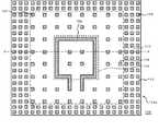
図1および図2は、本実施の形態における半導体装置100の構成を示す平面図である。図3は、図1および図2のA−A'断面図である。(First embodiment)
1 and 2 are plan views showing the configuration of the
図1は、高周波配線102が設けられた第1の配線層122a(第1の層)の平面図を示し、図2は、第1の配線層122aと半導体基板120との間に設けられた一の第2の配線層122b(第2の層)の平面図を示す。図2においては、平面視で高周波配線102に重なる領域を点線で示している。高周波配線102は、平面視でコイル状に形成されており、インダクタやトランスフォーマとして機能する。高周波配線102には、たとえば5GHz以上の周波数を有する電流が流れる。本実施の形態において、第1の配線層122aおよび各第2の配線層122bにそれぞれダミーメタル104が設けられる。ここで、ダミーメタルとは、その有無が半導体装置100の回路構成に影響を与えない導体パターンのことである。 FIG. 1 is a plan view of a
図1に示すように、第1の配線層122aにおいて、ダミーメタル104は、コイル状に形成された高周波配線102の内側および外側の両方に形成されている。また、図2に示すように、本実施の形態においては、ダミーメタル104は、平面視で高周波配線102と重なる領域にも設けられる。 As shown in FIG. 1, in the
図3に示すように、半導体装置100は、たとえばシリコン基板である半導体基板120と、半導体基板120上に設けられた多層配線層122とを含む。多層配線層122は、第1の配線層122a、第2の配線層122b、および第1の配線層122aの上に設けられた第3の配線層122c(第3の層)を含む。高周波配線102は、第1の配線層122aに設けられる。また、複数のダミーメタル104は、第1の配線層122a、第2の配線層122bおよび第3の配線層122c中にそれぞれ設けられる。第3の配線層122cは、図2に示した第2の配線層122bと同様の構成を有する。 As shown in FIG. 3, the
図1および図2に示すように、半導体装置100は、平面視で、高周波配線102の外縁で囲まれる第1の領域106と第1の領域106周囲の第2の領域108とを含む高周波配線近傍領域110と、高周波配線近傍領域110以外の外部領域112とを有する。ダミーメタル104は、高周波配線近傍領域110および外部領域112にそれぞれ分散配置される。本実施の形態において、いずれの層においても、平面視で、高周波配線近傍領域110のダミーメタル104間の平均間隔が、外部領域112のダミーメタル104間の平均間隔よりも広い。なお、各ダミーメタル104は実質的に同じ高さを有するため、本実施の形態において、各層においてダミーメタル104は、ダミーメタル104の単位体積あたりの量が、高周波配線近傍領域110中の方が外部領域112中よりも少なくなるように配置される。また、ダミーメタル104は、すべての層にわたるダミーメタル104の単位体積あたりの量が、高周波配線近傍領域110中の方が外部領域112中よりも少なくなるように配置される。 As shown in FIGS. 1 and 2, the
ダミーメタル104は、高周波配線102と同一の材料によって構成されている。かかる材料としては、銅またはアルミニウム等が挙げられる。高周波配線102およびダミーメタル104の材料が銅である場合、これらはたとえばダマシン法によって形成される。高周波配線102およびダミーメタル104は、同時に形成されることが好ましい。 The
図8は、インダクタとその周囲のダミーメタルの距離と、インダクタの特性との関係を示す図である。ここでは、高周波配線102として、4回巻きおよび5回巻きのインダクタをそれぞれ用いて3GHzの周波数を有する電流を流した。ダミーメタルは、インダクタと同層に設けた。インダクタとダミーメタルとの距離が50μm以上の場合は、4回巻きおよび5回巻きのいずれでも、インダクタのインダクタンス特性の変動はほとんどなかった。しかし、インダクタとダミーメタルの距離が30μm以下となると、インダクタのインダクタンス特性が劣化している。このような観点からは、たとえば、第2の領域108は、第1の領域106の周囲約50μm以上の範囲とすることができる。 FIG. 8 is a diagram illustrating the relationship between the distance between the inductor and the surrounding dummy metal and the characteristics of the inductor. Here, a current having a frequency of 3 GHz was passed using a 4-turn and 5-turn inductor as the high-
なお、たとえば第1の配線層122aの上に多数の第3の配線層122cが配置されている場合、高周波配線102の上面から所定の距離、たとえば50μm以上離れた上層の第3の配線層122cにおいては、平面視の全領域にわたってダミーメタル104が均等に配置されるようにすることもできる。高周波配線102から所定の距離を隔てた上方および側方においては、ダミーメタル104が高周波配線102の特性に及ぼす影響が小さいためである。 For example, when a large number of third wiring layers 122c are arranged on the
現在の微細CMOSプロセスでは、多層配線構造の各層のダミーメタルは、各層のレイアウトの情報や当該層における絶縁膜の材料等に基づき、プロセスが許容されるメタル密度よりある程度大きい密度となるように配置パターンが決定されている。本実施の形態において、外部領域112においては従来通りの密度でダミーメタル104の配置パターンを決定するとともに、高周波配線近傍領域110においては、プロセスが許容される範囲内の低い密度、たとえば最小値でダミーメタル104の配置パターンを決定する。以下、ダミーメタル104の配置パターンの決定手順を説明する。 In the current fine CMOS process, the dummy metal in each layer of the multilayer wiring structure is arranged so as to have a density that is somewhat higher than the metal density allowed for the process based on the layout information of each layer, the material of the insulating film in the layer, etc. The pattern has been determined. In the present embodiment, the arrangement pattern of the
図4は、ダミーメタル104の配置パターンの決定手順を示すフローチャートである。
まず、処理層を選択する(S100)。つづいて、当該層における半導体装置100の回路構成に必要な導体パターンのレイアウトの情報や当該層における絶縁膜の材料等に基づき、当該層において必要なメタル密度の許容範囲を算出する(S102)。この処理は、従来のダミーメタルの配置パターンを決定する処理と同様である。従来は、このようにして算出した必要なメタル密度範囲内のたとえば中程度以上のある程度大きいメタル密度となるようにダミーメタルの配置パターンが決定されている。FIG. 4 is a flowchart showing a procedure for determining the arrangement pattern of the
First, a processing layer is selected (S100). Subsequently, based on information on the layout of the conductor pattern necessary for the circuit configuration of the
つづいて、半導体装置100の平面図に基づき、高周波配線近傍領域110を選択する(S104)。次いで、高周波配線近傍領域110内におけるメタル密度を決定する。ここでは、S102で算出したメタル密度の許容範囲内の低い密度となるように高周波配線近傍領域110内のメタル密度を決定し、そのメタル密度となるようにダミーメタル104の配置パターンを決定する(S106)。たとえば、高周波配線近傍領域110のメタル密度は、S102で算出したメタル密度の許容範囲の最下限とすることができる。 Subsequently, the high frequency
つづいて、S102で算出したメタル密度の許容範囲内の高い密度となるように外部領域112内のメタル密度を決定し、そのメタル密度となるようにダミーメタル104の配置パターンを決定する(S108)。ここで、高い密度とは、S106で決定した高周波配線近傍領域110内のメタル密度よりも高いことをいう。外部領域112内のメタル密度は、従来と同様、S102で算出したメタル密度の許容範囲内のたとえば中程度以上となるようにすることができる。 Subsequently, the metal density in the
以上の処理を、全層が終了するまで(S110のYESとなるまで)繰り返す。本実施の形態においては、各層のレイアウトの情報や当該層における絶縁膜の材料等に応じて、各層毎にダミーメタル104のメタル密度を決定し、そのメタル密度となるようにダミーメタル104の配置パターンを決定する。そのため、各層毎にダミーメタル104の平均間隔や密度が異なることがある。しかし、いずれの層においても、高周波配線近傍領域110中のダミーメタル104の平均間隔または密度は、外部領域112中のダミーメタル104の平均間隔または密度よりも低くなるようにダミーメタル104の配置パターンが決定される。 The above processing is repeated until all layers are completed (until YES in S110). In the present embodiment, the metal density of the
本実施の形態の効果を説明する。
半導体装置100においては、高周波配線102の側方、上下の高周波配線近傍領域110において、それ以外の外部領域112よりもダミーメタル104の配置パターンを粗にしている。このように、高周波配線102の磁界の影響を強く受け易い領域において、ダミーメタル104の量を少なくすることにより、ダミーメタル104に発生する渦電流を抑制することができる。とくに、高周波配線102が形成された第1の配線層122aと半導体基板120との間においては、高周波配線近傍領域110に多数のダミーメタル104が配置されると、高周波配線102と半導体基板120との間の誘電体の厚さが小さくなるため、寄生容量が大きくなるという問題もある。本実施の形態においては、このような領域におけるダミーメタル104の量を必要最小限とすることにより、高周波配線102の特性の劣化を防ぐことができる。さらに、高周波配線近傍領域110においても、必要最小限のダミーメタル104が分散配置されるようにすることにより、エロージョンやディッシング等を効果的に防ぐこともできる。The effect of this embodiment will be described.
In the
本実施の形態において高周波配線102はインダクタである。この場合、上記渦電流によりインダクタの磁界を打ち消す方向の磁界が発生すると、結果としてインダクタの磁界の強度が低下する。磁界の強度の低下は、インダクタのQ値の劣化につながってしまう。この点、本実施の形態によれば、上述のとおり渦電流を抑制できるので、かかるQ値の劣化を小さく抑えることができる。 In the present embodiment, the high-
上述の問題、すなわちダミーメタル104の渦電流により高周波配線102の回路定数が変動するという問題は、5GHz以上の電流が高周波配線102を流れる場合に顕著となる。したがって、この場合には、ダミーメタル104に発生する渦電流を抑制できる本実施の形態の有用性が、特に高まる。 The above-described problem, that is, the problem that the circuit constant of the high-
(第2の実施の形態)
本実施の形態においては、高周波配線102の周囲の高周波配線近傍領域110と外部領域112との間に、ガードリング116が設けられている点で、図1から図3を参照して説明した第1の実施の形態における半導体装置100と異なる。なお、本実施の形態においても高周波配線102はインダクタである。(Second Embodiment)
In the present embodiment, the guard ring 116 is provided between the high-frequency
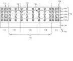
図5および図6は、本実施の形態における半導体装置100の構成を示す平面図である。図7は、図6のB−B'断面図である。図5は、高周波配線102が設けられた第1の配線層122a(第1の層)の平面図を示し、図6は、第1の配線層122aと半導体基板120との間に設けられた第2の配線層122b(第2の層)の平面図を示す。 5 and 6 are plan views showing the configuration of the
図7に示すように、ガードリング116は、多層配線層122のすべての層にわたって連続して形成された構成とすることができる。とくに限定されないが、ビア層においては、ガードリング116は、スリットビアにより構成することもできる。 As shown in FIG. 7, the guard ring 116 may be formed continuously over all the layers of the
ここで、ガードリング116が外部領域112内に設けられた例を示しているが、ガードリング116は、高周波配線近傍領域110と外部領域112との境界に設けることができ、高周波配線近傍領域110と外部領域112とは、ガードリング116により区画されるようにすることもできる。すなわち、従来から、高周波配線102の周囲をガードリング116で囲む構成が採用されることがある。そのような構成の場合は、ガードリング116内を高周波配線近傍領域110として、ガードリング116外を外部領域112として、ダミーメタル104の配置パターンをそれぞれ決定することができる。ガードリングは、外部領域に形成される素子に対して、高周波配線により生じる影響を低減するために設けられる。ガードリングは、たとえば接地電位に接続される。 Here, an example in which the guard ring 116 is provided in the
本実施の形態においても、第1の実施の形態と同様の効果を得ることができる。 Also in this embodiment, the same effect as that of the first embodiment can be obtained.
以上、図面を参照して本発明の実施形態について述べたが、これらは本発明の例示であり、上記以外の様々な構成を採用することもできる。 As mentioned above, although embodiment of this invention was described with reference to drawings, these are the illustrations of this invention, Various structures other than the above are also employable.
以上の実施の形態においては、高周波配線102が一つの第1の配線層122aに形成された構成を示したが、高周波配線102は、複数の配線層にわたって形成された構成とすることもできる。この場合も、高周波配線102が形成された各層において、高周波配線近傍領域110においては外部領域112よりもダミーメタル104間の平均間隔が大きくなるようにダミーメタル104を分散配置することができる。 In the above-described embodiment, the configuration in which the high-
さらに、以上の実施の形態においては、高周波配線102が平面視でコイル状である場合を例として説明したが、高周波配線102は平面視でじぐざぐ状や、半導体基板120に水平な方向に中心軸の輪を形成するトロイダル状等種々の形状とすることができる。この場合も、平面視で高周波配線102が配置された領域の外縁で囲まれる第1の領域とその周囲の第2の領域とを含む領域を高周波配線近傍領域110とすることができる。 Furthermore, in the above embodiment, the case where the high-
なお、半導体装置100の多層配線層122がシングルダマシンプロセスで形成される場合、ビア層には、ダミーメタル104が形成されない構成としてもよい。ビア層では、配線層に比べてCMP工程におけるプロセスばらつきの原因となるディッシング等が発生しないためである。ただし、ビア層にもダミーメタル104を設けてもよい。 In the case where the
100 半導体装置
102 高周波配線
104 ダミーメタル
106 第1の領域
108 第2の領域
110 高周波配線近傍領域
112 外部領域
116 ガードリング
120 半導体基板
122 多層配線層
122a 第1の配線層
122b 第2の配線層
122c 第3の配線層DESCRIPTION OF
Claims (6)
Translated fromJapanese前記半導体基板上に設けられた多層配線層と、
前記多層配線層の一つの配線層に設けられた平面視でコイル状の高周波配線と、
前記多層配線層内で前記高周波配線と同じ配線層に設けられ、前記高周波配線の内側に配置された複数の第1ダミーメタルと、
前記多層配線層内で前記高周波配線と同じ配線層に設けられ、前記高周波配線の外側に配置された複数の第2ダミーメタルと、
前記多層配線層内で前記高周波配線を構成する配線層よりも一つ下層に設けられた配線層に設けられ、平面視して前記高周波配線の内側で前記高周波配線と重ならない部分に配置された複数の第3ダミーメタルと、
前記多層配線層内で前記複数の第3ダミーメタルと同じ配線層に設けられ、平面視して前記高周波配線の外側に配置された複数の第4ダミーメタルと、
前記多層配線層内で前記複数の第3ダミーメタルと同じ配線層に設けられ、平面視して前記高周波配線と重なるように配置された複数の第5ダミーメタルと、
前記多層配線層中に、平面視で前記高周波配線を囲むように設けられたガードリングと、
前記多層配線層内で前記高周波配線と同じ配線層に設けられ、前記ガードリングの外側に配置された複数の第6ダミーメタルとを有し、
前記複数の第2ダミーメタルは前記ガードリングの内側に設けられ、
前記複数の第1ダミーメタルの平均密度、及び、前記複数の第2ダミーメタルの平均密度は、前記複数の第6ダミーメタルの平均密度よりも低い半導体装置。A semiconductor substrate;
A multilayer wiring layer provided on the semiconductor substrate;
A coil-like high-frequency wiring in a plan view provided in one wiring layer of the multilayer wiring layer;
And wherein the multilayer wiring layer provided on the same wiring layer as the high-frequency wiring, the high-frequencywiring plurality of which are disposed insidethe first dummy metal,
Wherein a multilayer wiring layer provided on the same wiring layer as the high-frequency wiring, and a plurality of second dummy metal disposed outsideof the high-frequencywiring,
Than said wiring layer constituting the high-frequency wiring multilayer wiring layer provided on the wiring layer provided on one lower layer, is arranged in the portion not overlapping with the high-frequency wiringinner sideof the high-frequency wiring in plan view A plurality of third dummy metals,
Wherein provided in the same wiring layer as the plurality of third dummy metal in a multilayer wiring layer, and a plurality of fourth dummy metal disposed outsideof the high-frequencywiring in plan view,
A plurality of fifth dummy metals provided in the same wiring layer as the plurality of third dummy metals in the multilayer wiring layer, and arranged so as to overlap the high-frequency wirings in plan view;
A guard ring provided in the multilayer wiring layer so as to surround the high-frequency wiring in a plan view;
A plurality of sixth dummy metals provided in the same wiring layer as the high-frequency wiring in the multilayer wiring layer and disposed outside the guard ring;
The plurality of second dummy metals are provided inside the guard ring,
A semiconductor device in which an average density of the plurality of first dummy metals and an average density ofthe plurality of second dummy metals are lower than an average density of the plurality of sixth dummy metals.
前記半導体基板上に設けられた多層配線層と、
前記多層配線層の一つの配線層に設けられた平面視でコイル状の高周波配線と、
前記多層配線層内で前記高周波配線と同じ配線層に設けられ、前記高周波配線の付近に配置された複数の第1ダミーメタルと、
前記多層配線層内で前記高周波配線と同じ配線層に設けられ、前記高周波配線の付近よりも外側に配置された複数の第2ダミーメタルと、
前記多層配線層内で前記高周波配線を構成する配線層よりも一つ下層に設けられた配線層に設けられ、平面視して前記高周波配線の付近で前記高周波配線と重ならない部分に配置された複数の第3ダミーメタルと、
前記多層配線層内で前記複数の第3ダミーメタルと同じ配線層に設けられ、平面視して前記高周波配線の付近よりも外側に配置された複数の第4ダミーメタルと、
前記多層配線層内で前記複数の第3ダミーメタルと同じ配線層に設けられ、平面視して前記高周波配線と重なるように配置された複数の第5ダミーメタルと、
前記多層配線層中に、平面視で前記高周波配線を囲むように設けられたガードリングとを有し、
前記複数の第1ダミーメタルの平均密度は、前記複数の第2ダミーメタルの平均密度よりも低く、
前記複数の第1ダミーメタルは前記ガードリングの内側に設けられ、前記複数の第2ダミーメタルは前記ガードリングの外側に設けられている、
半導体装置。A semiconductor substrate;
A multilayer wiring layer provided on the semiconductor substrate;
A coil-like high-frequency wiring in a plan view provided in one wiring layer of the multilayer wiring layer;
Wherein provided in a multilayer wiring layer in the same wiring layer and the high-frequency lines, a plurality of first dummy metal disposedwith the nearof the high frequency line,
Wherein provided in a multilayer wiring layer in the same wiring layer and the high-frequency lines, and a plurality of second dummy metal disposed outside than thebiasing nearthe high-frequency line,
Than said wiring layer constituting the high-frequency wiring multilayer wiring layer provided on the wiring layer provided on one lower layer, disposed on the do not overlap with the frequency wiring portion in the nearurging of the high-frequency wiring in plan view A plurality of third dummy metals,
Wherein provided in a multilayer wiring layer in the same wiring layer as the plurality of third dummy metal, and a plurality of fourth dummy metal than nearthe urging of the high frequency line arranged outside in plan view,
A plurality of fifth dummy metals provided in the same wiring layer as the plurality of third dummy metals in the multilayer wiring layer, and arranged so as to overlap the high-frequency wirings in plan view;
In the multilayer wiring layer, having a guard ring provided so as to surround the high-frequency wiring in a plan view,
The average density of the plurality of first dummy metals is lower than the average density of the plurality of second dummy metals,
The plurality of first dummy metals are provided inside the guard ring, and the plurality of second dummy metals are provided outside the guard ring,
Semiconductor device.
前記高周波配線は、インダクタとして機能する半導体装置。The semiconductor device according to claim 1or 2 ,
The high-frequency wiring is a semiconductor device that functions as an inductor.
前記半導体基板上に、多層配線層の一つの配線層として第2配線層を形成する工程と、
前記第2配線層に複数の第3ダミーメタル、複数の第4ダミーメタル、および複数の第5ダミーメタルを形成する工程と、
前記第2配線層より一つ上層に、前記多層配線層の一つの配線層として第1配線層を形成する工程と、
前記第1配線層に平面視でコイル状の高周波配線と複数の第1ダミーメタルと複数の第2ダミーメタルと複数の第6ダミーメタルとを形成する工程と、
前記多層配線層中に、平面視で前記高周波配線を囲むように設けられたガードリングを形成する工程とを有し、
前記複数の第1ダミーメタルは前記高周波配線の内側に形成され、
前記複数の第2ダミーメタルは前記高周波配線の外側かつ前記ガードリングの内側に形成され、
前記複数の第3ダミーメタルは平面視して前記高周波配線の内側で前記高周波配線と重ならない部分に形成され、
前記複数の第4ダミーメタルは平面視して前記高周波配線の外側に形成され、
前記複数の第5ダミーメタルは平面視して前記高周波配線と重なるように形成され、
前記複数の第6ダミーメタルは、ガードリングの外側に形成され、
平面視で見て、前記複数の第1ダミーメタルの平均密度、及び、前記複数の第2ダミーメタルの平均密度は、前記複数の第6ダミーメタルの平均密度よりも低くなるように形成される半導体装置の製造方法。Preparing a semiconductor substrate; and
Forming a second wiring layer on the semiconductor substrate as one wiring layer of a multilayer wiring layer;
Forming a plurality of third dummy metals, a plurality of fourth dummy metals, and a plurality of fifth dummy metals in the second wiring layer;
Forming a first wiring layer as one wiring layer of the multilayer wiring layer, one layer above the second wiring layer;
Forming a coil-shaped high-frequency wiring, a plurality of first dummy metals, a plurality of second dummy metals, and a plurality of sixth dummy metals in a plan view on the first wiring layer;
Forming a guard ring provided to surround the high-frequency wiring in a plan view in the multilayer wiring layer,
Wherein the plurality of first dummy metal is formed on theinner sideof the high frequency line,
Wherein the plurality of second dummy metal formed inside theouter side and the guard ringof the high-frequency line,
Said plurality of third dummy metal is formed in a portion that does not overlap with the high-frequency wiringinner sideof the high-frequency wiring in plan view,
It said plurality of fourth dummy metal is formed on theouter sideof the high-frequency wiring in plan view,
The plurality of fifth dummy metals are formed so as to overlap the high-frequency wiring in plan view,
The plurality of sixth dummy metals are formed outside the guard ring,
When viewed in a plan view, the average density of the plurality of first dummy metals and the average density ofthe plurality of second dummy metals are formed to be lower than the average density of the plurality of sixth dummy metals. A method for manufacturing a semiconductor device.
前記半導体基板上に、多層配線層の一つの配線層として第2配線層を形成する工程と、
前記第2配線層に複数の第3ダミーメタル、複数の第4ダミーメタル、および複数の第5ダミーメタルを形成する工程と、
前記第2配線層より一つ上層に、前記多層配線層の一つの配線層として第1配線層を形成する工程と、
前記第1配線層に平面視でコイル状の高周波配線と複数の第1ダミーメタルと複数の第2ダミーメタルを形成する工程と、
前記多層配線層中に、平面視で前記高周波配線を囲むように設けられたガードリングを形成する工程とを有し、
前記複数の第1ダミーメタルは前記高周波配線の付近に形成され、
前記複数の第2ダミーメタルは前記高周波配線の付近よりも外側に形成され、
前記複数の第3ダミーメタルは平面視して前記高周波配線の付近で前記高周波配線と重ならない部分に形成され、
前記複数の第4ダミーメタルは平面視して前記高周波配線の付近よりも外側に形成され、
前記複数の第5ダミーメタルは平面視して前記高周波配線と重なるように形成され、
平面視で見て、前記複数の第1ダミーメタルの平均密度は、前記複数の第2ダミーメタルの平均密度よりも低くなるように形成され、
前記複数の第1ダミーメタルは前記ガードリングの内側に形成され、前記複数の第2ダミーメタルは前記ガードリングの外側に形成される半導体装置の製造方法。Preparing a semiconductor substrate; and
Forming a second wiring layer on the semiconductor substrate as one wiring layer of a multilayer wiring layer;
Forming a plurality of third dummy metals, a plurality of fourth dummy metals, and a plurality of fifth dummy metals in the second wiring layer;
Forming a first wiring layer as one wiring layer of the multilayer wiring layer, one layer above the second wiring layer;
Forming a coil-shaped high-frequency wiring, a plurality of first dummy metals, and a plurality of second dummy metals in a plan view on the first wiring layer;
Forming a guard ring provided to surround the high-frequency wiring in a plan view in the multilayer wiring layer,
Wherein the plurality of first dummy metal formed in the proximalurging of the high frequency line,
Wherein the plurality of second dummy metal formed outside the proximalurging of the high frequency line,
Said plurality of third dummy metal is formed in a portion that does not overlap with the high-frequency wiring nearthe urging of the high-frequency wiring in plan view,
It said plurality of fourth dummy metal is formed on the outer side than the nearurging of the high-frequency wiring in plan view,
The plurality of fifth dummy metals are formed so as to overlap the high-frequency wiring in plan view,
When viewed in a plan view, an average density of the plurality of first dummy metals is formed to be lower than an average density of the plurality of second dummy metals,
The method of manufacturing a semiconductor device, wherein the plurality of first dummy metals are formed inside the guard ring, and the plurality of second dummy metals are formed outside the guard ring.
前記高周波配線は、インダクタとして機能する半導体装置の製造方法。In the manufacturing method of the semiconductor device according to claim4 or 5 ,
The method of manufacturing a semiconductor device in which the high-frequency wiring functions as an inductor.
Priority Applications (1)
| Application Number | Priority Date | Filing Date | Title |
|---|---|---|---|
| JP2012179806AJP5912071B2 (en) | 2012-08-14 | 2012-08-14 | Semiconductor device and manufacturing method of semiconductor device |
Applications Claiming Priority (1)
| Application Number | Priority Date | Filing Date | Title |
|---|---|---|---|
| JP2012179806AJP5912071B2 (en) | 2012-08-14 | 2012-08-14 | Semiconductor device and manufacturing method of semiconductor device |
Related Parent Applications (1)
| Application Number | Title | Priority Date | Filing Date |
|---|---|---|---|
| JP2007264766ADivisionJP5156324B2 (en) | 2007-10-10 | 2007-10-10 | Semiconductor device and manufacturing method of semiconductor device |
Related Child Applications (1)
| Application Number | Title | Priority Date | Filing Date |
|---|---|---|---|
| JP2014219876ADivisionJP5938084B2 (en) | 2014-10-29 | 2014-10-29 | Semiconductor device |
Publications (2)
| Publication Number | Publication Date |
|---|---|
| JP2012248881A JP2012248881A (en) | 2012-12-13 |
| JP5912071B2true JP5912071B2 (en) | 2016-04-27 |
Family
ID=47468981
Family Applications (1)
| Application Number | Title | Priority Date | Filing Date |
|---|---|---|---|
| JP2012179806AActiveJP5912071B2 (en) | 2012-08-14 | 2012-08-14 | Semiconductor device and manufacturing method of semiconductor device |
Country Status (1)
| Country | Link |
|---|---|
| JP (1) | JP5912071B2 (en) |
Family Cites Families (5)
| Publication number | Priority date | Publication date | Assignee | Title |
|---|---|---|---|---|
| JP2004153015A (en)* | 2002-10-30 | 2004-05-27 | Fujitsu Ltd | Semiconductor device and manufacturing method thereof |
| JP4141881B2 (en)* | 2003-04-04 | 2008-08-27 | シャープ株式会社 | Integrated circuit |
| US7262481B1 (en)* | 2004-12-16 | 2007-08-28 | Nxp B.V. | Fill structures for use with a semiconductor integrated circuit inductor |
| JP4785060B2 (en)* | 2006-01-05 | 2011-10-05 | 株式会社東芝 | Semiconductor device, manufacturing method thereof, and pattern generation method thereof |
| JP4908035B2 (en)* | 2006-03-30 | 2012-04-04 | 株式会社東芝 | Semiconductor integrated circuit |
- 2012
- 2012-08-14JPJP2012179806Apatent/JP5912071B2/enactiveActive
Also Published As
| Publication number | Publication date |
|---|---|
| JP2012248881A (en) | 2012-12-13 |
Similar Documents
| Publication | Publication Date | Title |
|---|---|---|
| JP5156324B2 (en) | Semiconductor device and manufacturing method of semiconductor device | |
| JP5180625B2 (en) | Semiconductor device | |
| JP5818694B2 (en) | Magnetic film reinforced inductor | |
| CN100375283C (en) | Semiconductor device | |
| CN102832193B (en) | The integrated circuit inductor of conductor with winding | |
| EP2958144A1 (en) | Integrated transformer | |
| JP2006528837A (en) | Inductive and capacitive elements for semiconductor technology with minimum pattern density requirements | |
| CN104051435B (en) | Inductor structure and method with pseudo- metal parts | |
| JP5938084B2 (en) | Semiconductor device | |
| JP4647484B2 (en) | Semiconductor device | |
| JP6109385B2 (en) | Semiconductor device | |
| US6833781B1 (en) | High Q inductor in multi-level interconnect | |
| JP5912071B2 (en) | Semiconductor device and manufacturing method of semiconductor device | |
| JP2010080551A (en) | Semiconductor device | |
| US20120032297A1 (en) | Electronic Device and Method for Fabricating the Same, Spiral Inductor Device and Method for Fabricating the Same | |
| KR100779981B1 (en) | High Performance Integrated Inductor | |
| KR101116897B1 (en) | Solenoid inductor for frequency synthesizer in digital cmos process | |
| US9859356B2 (en) | Semiconductor integrated circuit |
Legal Events
| Date | Code | Title | Description |
|---|---|---|---|
| A977 | Report on retrieval | Free format text:JAPANESE INTERMEDIATE CODE: A971007 Effective date:20131129 | |
| A131 | Notification of reasons for refusal | Free format text:JAPANESE INTERMEDIATE CODE: A131 Effective date:20131203 | |
| A977 | Report on retrieval | Free format text:JAPANESE INTERMEDIATE CODE: A971007 Effective date:20131211 | |
| A521 | Written amendment | Free format text:JAPANESE INTERMEDIATE CODE: A523 Effective date:20140131 | |
| A131 | Notification of reasons for refusal | Free format text:JAPANESE INTERMEDIATE CODE: A131 Effective date:20140408 | |
| A521 | Written amendment | Free format text:JAPANESE INTERMEDIATE CODE: A523 Effective date:20140604 | |
| A02 | Decision of refusal | Free format text:JAPANESE INTERMEDIATE CODE: A02 Effective date:20140729 | |
| A521 | Written amendment | Free format text:JAPANESE INTERMEDIATE CODE: A523 Effective date:20141029 | |
| A911 | Transfer of reconsideration by examiner before appeal (zenchi) | Free format text:JAPANESE INTERMEDIATE CODE: A911 Effective date:20141106 | |
| A912 | Removal of reconsideration by examiner before appeal (zenchi) | Free format text:JAPANESE INTERMEDIATE CODE: A912 Effective date:20141128 | |
| A521 | Written amendment | Free format text:JAPANESE INTERMEDIATE CODE: A523 Effective date:20151027 | |
| A521 | Written amendment | Free format text:JAPANESE INTERMEDIATE CODE: A523 Effective date:20160126 | |
| A61 | First payment of annual fees (during grant procedure) | Free format text:JAPANESE INTERMEDIATE CODE: A61 Effective date:20160331 | |
| R150 | Certificate of patent or registration of utility model | Ref document number:5912071 Country of ref document:JP Free format text:JAPANESE INTERMEDIATE CODE: R150 |