JP5906407B2 - Gas component detector - Google Patents
Gas component detectorDownload PDFInfo
- Publication number
- JP5906407B2 JP5906407B2JP2011086891AJP2011086891AJP5906407B2JP 5906407 B2JP5906407 B2JP 5906407B2JP 2011086891 AJP2011086891 AJP 2011086891AJP 2011086891 AJP2011086891 AJP 2011086891AJP 5906407 B2JP5906407 B2JP 5906407B2
- Authority
- JP
- Japan
- Prior art keywords
- light
- light receiving
- gas component
- component detection
- detection device
- Prior art date
- Legal status (The legal status is an assumption and is not a legal conclusion. Google has not performed a legal analysis and makes no representation as to the accuracy of the status listed.)
- Expired - Fee Related
Links
Images


Classifications
- G—PHYSICS
- G01—MEASURING; TESTING
- G01N—INVESTIGATING OR ANALYSING MATERIALS BY DETERMINING THEIR CHEMICAL OR PHYSICAL PROPERTIES
- G01N21/00—Investigating or analysing materials by the use of optical means, i.e. using sub-millimetre waves, infrared, visible or ultraviolet light
- G01N21/17—Systems in which incident light is modified in accordance with the properties of the material investigated
- G01N21/25—Colour; Spectral properties, i.e. comparison of effect of material on the light at two or more different wavelengths or wavelength bands
- G01N21/31—Investigating relative effect of material at wavelengths characteristic of specific elements or molecules, e.g. atomic absorption spectrometry
- G01N21/35—Investigating relative effect of material at wavelengths characteristic of specific elements or molecules, e.g. atomic absorption spectrometry using infrared light
- G01N21/3504—Investigating relative effect of material at wavelengths characteristic of specific elements or molecules, e.g. atomic absorption spectrometry using infrared light for analysing gases, e.g. multi-gas analysis
Landscapes
- Physics & Mathematics (AREA)
- Spectroscopy & Molecular Physics (AREA)
- General Health & Medical Sciences (AREA)
- Chemical & Material Sciences (AREA)
- Analytical Chemistry (AREA)
- Biochemistry (AREA)
- Life Sciences & Earth Sciences (AREA)
- General Physics & Mathematics (AREA)
- Immunology (AREA)
- Pathology (AREA)
- Health & Medical Sciences (AREA)
- Investigating Or Analysing Materials By Optical Means (AREA)
- Optical Measuring Cells (AREA)
Description
Translated fromJapanese本発明は、赤外線の吸収特性を利用して気体成分の濃度を検出する気体成分検出装置に関する。 The present invention relates to a gas component detection device that detects the concentration of a gas component using infrared absorption characteristics.
従来の気体成分検出装置として、特許文献1に記載されている赤外線式ガス検出器や特許文献2に記載されている赤外線ガス分析計などがある。 As a conventional gas component detection device, there are an infrared gas detector described in
引用文献1記載の従来例は、検出対象の気体(例えば、一酸化炭素など)が内部に導入されるハウジングと、ハウジング内に赤外線を照射する光源と、ハウジング内の赤外線を検出する赤外線検出器とを備える。光源は、発光ダイオードチップ(ベア素子)、ベア素子が実装されるステム、ベア素子を封止する封止材などで構成されるパッケージ型の発光ダイオードからなり、ステムに突設されるリード端子から給電されて発光する。また、赤外線検出器は、フォトダイオードチップ(ベア素子)、ベア素子が実装されるステム、ベア素子を封止する封止材などで構成されるパッケージ型のフォトダイオードからなり、ステムに突設されるリード端子から検出信号が取り出される。さらに、赤外線検出器には、検出対象の気体に吸収される赤外線の波長帯域を通過域に含む波長フィルタ(波長選択フィルタ)が設けられている。この従来例では、ハウジングの内部に楕円体形状の空間が形成され、当該楕円体の2つの焦点に発光ダイオードチップ並びにフォトダイオードチップが位置している。一方、引用文献2記載の従来例は、箱形の金属ケース、金属ケース内に配設される楕円反射鏡、楕円反射鏡の反射面と対向して配置される光源及び受光器、受光器の受光面に設けられて検出対象の気体に吸収される赤外線の波長帯域を通過域に含む波長フィルタなどを備える。金属ケースには通気孔が設けられ、検出対象の気体(例えば、二酸化炭素)を含む気体が当該通気孔を通して金属ケース内に導入される。そして、光源から照射される赤外線のうちで検出対象の気体に吸収されずに赤外線検出器や受光器で受光される赤外線の量(レベル)に応じて、ハウジングや金属ケース内に存在する検出対象の気体の濃度を検出することができる。 The conventional example described in the cited
ところで、従来例に用いられる波長フィルタは、通常、誘電体多層膜からなるバンドパスフィルタ(干渉フィルタ)で構成されているため、入射角依存性が高いという欠点がある。つまり、特許文献1や特許文献2に記載されている従来例の場合、通過域に属する波長の赤外線のうちで光源から放射された後に楕円体の内面や楕円反射鏡の反射面で反射した赤外線の大部分が波長フィルタを通過できなくなる虞がある。そして、波長フィルタを通過して赤外線検出器や受光器に到達する赤外線の量が減少すれば、気体成分の検出精度が低下してしまうことになる。 Incidentally, since the wavelength filter used in the conventional example is usually composed of a bandpass filter (interference filter) made of a dielectric multilayer film, there is a drawback that the incident angle dependency is high. In other words, in the case of the conventional examples described in
本発明は、上記課題に鑑みて為されたものであり、波長フィルタの入射角依存性に起因した赤外線受光量の減少を抑制することを目的とする。 The present invention has been made in view of the above problems, and an object of the present invention is to suppress a decrease in the amount of received infrared light due to the incident angle dependence of a wavelength filter.
本発明の気体成分検出装置は、赤外線を放射する1乃至複数の発光部と、赤外線を受光して電気信号に変換する1乃至複数の受光部と、前記発光部及び前記受光部を保持する保持体と、前記発光部から放射される赤外線を前記受光部の受光面まで導光する導光体と、検出対象である気体に吸収される波長帯域を通過域に含み且つ前記導光体に導光される前記赤外線の光路上に配置される波長フィルタとを備え、当該導光体は、前記発光部に対向する第1反射鏡と、前記受光部の受光面に対向する第2反射鏡と、前記第1反射鏡と前記第2反射鏡が両端に配置された第3反射鏡とを有することを特徴とする。 The gas component detection device of the present invention includes one or more light emitting units that emit infrared rays, one or more light receiving units that receive infrared rays and convert them into electrical signals, and a holder that holds the light emitting units and the light receiving units. A light guide that guides infrared rays radiated from the light emitting unit to the light receiving surface of the light receiving unit, and a wavelength band that is absorbed by the gas that is the detection target, and is guided to the light guide. A wavelength filter disposed on the optical path of the infrared light that is emitted, and the light guide includes a first reflecting mirror that faces the light emitting portion, and a second reflecting mirror that faces the light receiving surface of the light receiving portion. The first reflecting mirror and the second reflecting mirror have third reflecting mirrors disposed at both ends.
この気体成分検出装置において、前記導光体は、前記第1反射鏡で反射された赤外線の光路を分岐する分岐部と、当該分岐部で分岐された複数の前記光路上にそれぞれ配置される複数の前記第2反射鏡とを有することが好ましい。 In this gas component detection device, the light guide body includes a branching portion that branches the optical path of the infrared light reflected by the first reflecting mirror, and a plurality of light guides disposed on the plurality of optical paths branched by the branching portion. The second reflecting mirror is preferably included.
この気体成分検出装置において、前記発光部と前記受光部と前記波長フィルタと前記導光体の組み合わせを複数組備えることが好ましい。 In this gas component detection device, it is preferable that a plurality of combinations of the light emitting unit, the light receiving unit, the wavelength filter, and the light guide are provided.
この気体成分検出装置において、前記第1反射鏡は放物面形状の反射面を有し、当該放物面の焦点の位置に前記発光部が配置されることが好ましい。 In this gas component detection device, it is preferable that the first reflecting mirror has a parabolic reflecting surface, and the light emitting unit is arranged at a focal point of the parabolic surface.
この気体成分検出装置において、前記第2反射鏡は曲面形状の反射面を有することが好ましい。 In this gas component detection device, it is preferable that the second reflecting mirror has a curved reflecting surface.
この気体成分検出装置において、前記発光部は赤外線を放射する半導体ベアチップからなり、前記受光部は赤外線を受光して電気信号に変換する半導体ベアチップからなることが好ましい。 In this gas component detection device, it is preferable that the light emitting unit is a semiconductor bare chip that emits infrared light, and the light receiving unit is a semiconductor bare chip that receives infrared light and converts it into an electrical signal.
この気体成分検出装置において、検出対象である気体に吸収される波長帯域を通過域に含む主波長フィルタと、当該主波長フィルタの前記通過域を含まず且つ当該通過域近傍の波長帯域を通過域に含む副波長フィルタと、前記主波長フィルタを通過する赤外線を受光する前記受光部と、当該受光部とは別の前記受光部であり且つ前記副波長フィルタを通過する赤外線を受光する前記受光部とを備えることが好ましい。 In this gas component detection device, a main wavelength filter that includes a wavelength band that is absorbed by the gas to be detected in the pass band, and a pass band that does not include the pass band of the main wavelength filter and is in the vicinity of the pass band. A sub-wavelength filter included in the light-receiving unit, the light-receiving unit that receives infrared light that passes through the main-wavelength filter, and the light-receiving unit that is the light-receiving unit different from the light-receiving unit and receives infrared light that passes through the sub-wavelength filter It is preferable to comprise.
この気体成分検出装置において、前記受光部から出力される電気信号を信号処理する信号処理回路部を備え、当該信号処理回路部は、前記導光体の外側において前記発光部と前記受光部に挟まれた位置に配置されることが好ましい。 The gas component detection device includes a signal processing circuit unit that performs signal processing on an electrical signal output from the light receiving unit, and the signal processing circuit unit is sandwiched between the light emitting unit and the light receiving unit outside the light guide. It is preferable to be arranged at a predetermined position.
この気体成分検出装置において、前記信号処理回路部と前記光路との間に第4反射鏡が配置されることが好ましい。 In this gas component detection device, it is preferable that a fourth reflecting mirror is disposed between the signal processing circuit unit and the optical path.
この気体成分検出装置において、前記第4反射鏡は、一面を反射面とする平板状に形成され、当該反射面が前記発光部の発光面と面一となるように前記保持体に保持されることが好ましい。 In this gas component detection device, the fourth reflecting mirror is formed in a flat plate shape having one surface as a reflecting surface, and is held by the holding body so that the reflecting surface is flush with the light emitting surface of the light emitting unit. It is preferable.
この気体成分検出装置において、前記発光部と前記信号処理回路部との間に、前記発光部から放射される赤外線を遮蔽する壁が設けられることが好ましい。 In this gas component detection device, it is preferable that a wall that shields infrared rays emitted from the light emitting unit is provided between the light emitting unit and the signal processing circuit unit.
この気体成分検出装置において、前記壁は前記保持体と一体に形成されることが好ましい。 In this gas component detection device, the wall is preferably formed integrally with the holding body.
この気体成分検出装置において、前記波長フィルタは前記受光部とともに前記保持体に保持されることが好ましい。 In this gas component detection device, it is preferable that the wavelength filter is held by the holding body together with the light receiving unit.
この気体成分検出装置において、前記波長フィルタは前記導光体の内部に収納されることが好ましい。 In this gas component detection device, it is preferable that the wavelength filter is housed inside the light guide.
この気体成分検出装置において、前記発光部と前記導光体の間の光路上に集光用のレンズが配置されることが好ましい。 In this gas component detection device, it is preferable that a condensing lens is disposed on an optical path between the light emitting unit and the light guide.
この気体成分検出装置において、前記波長フィルタは前記受光部に取り付けられることが好ましい。 In this gas component detection device, the wavelength filter is preferably attached to the light receiving unit.
この気体成分検出装置において、前記保持体は、前記発光部及び前記受光部への配線が一体に形成される立体配線基板であることが好ましい。 In this gas component detection device, the holding body is preferably a three-dimensional wiring board in which wirings to the light emitting unit and the light receiving unit are integrally formed.
この気体成分検出装置において、前記導光体を保持して前記保持体と結合されるカバーを備え、当該カバーの前記保持体との結合面に1乃至複数の突起が設けられ、当該突起と嵌合する嵌合孔が前記保持体の前記結合面に設けられ、当該嵌合孔よりも小径の孔が当該嵌合孔の底面に設けられることが好ましい。 The gas component detection device includes a cover that holds the light guide and is coupled to the holding body, and one or a plurality of protrusions are provided on a coupling surface of the cover with the holding body. It is preferable that a fitting hole to be fitted is provided on the coupling surface of the holding body, and a hole having a smaller diameter than the fitting hole is provided on the bottom surface of the fitting hole.
本発明の気体成分検出装置は、波長フィルタの入射角依存性に起因した赤外線受光量の減少を抑制することができるという効果がある。 The gas component detection device of the present invention has an effect that it can suppress a decrease in the amount of received infrared light due to the incident angle dependence of the wavelength filter.
(実施形態1)
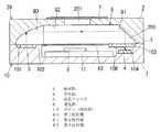
本実施形態の気体成分検出装置(以下、ガスセンサと呼ぶ。)は、図2に示すように回路ブロック1と光学ブロック2で構成されている。なお、以下の説明では、図2において上下左右前後を規定する。(Embodiment 1)
A gas component detection device (hereinafter referred to as a gas sensor) of this embodiment is composed of a
回路ブロック1は、合成樹脂成形体からなるボディ10の内部に発光部3、受光部4、波長フィルタ5、信号処理回路部6を実装した配線板11などが収納されて構成される。発光部3は、赤外線を放射する半導体ベアチップ(例えば、発光ダイオードチップや半導体基板上にMEMS技術を用いた抵抗素子が形成されてなる光源)からなる。ただし、発光部3から放射される赤外線の波長は、検出対象の気体(例えば、一酸化炭素や二酸化炭素、メタン、窒素酸化物など)に吸収され易い波長である。また受光部4は、赤外線を受光して電気信号に変換する半導体ベアチップ(例えば、フォトダイオードチップや焦電素子)からなる。波長フィルタ5は、発光部3から放射される赤外線の波長を含む波長帯域を通過域に含むバンドパスフィルタからなる。この種のバンドパスフィルタは干渉フィルタとも呼ばれ、主に誘電体膜の多層構造を有している。信号処理回路部6は、発光部3を駆動して赤外線を照射させたり、受光部4から出力される信号に対して増幅や波形整形、サンプリング、A/D変換、演算処理、補正処理、異常濃度判定処理などの信号処理を行う集積回路(IC)からなる。 The
配線板11は、図3に示すように長方形状の主部11Aと、主部11Aよりも小さい長方形状であって主部11Aの左後端より左方へ突出する延長部11Bとが一体に形成されている。主部11Aのほぼ中央に信号処理回路部6が実装され、図示しないプリント配線が主部11Aの上面及び延長部11Bの上面に形成されている。 As shown in FIG. 3, the
ボディ10は、扁平な直方体形状に形成されるとともに上面側に開口する凹所100が設けられ、この凹所100内に配線板11を収納する。また、ボディ10の上面側における左端部には、凹部101が形成されており、この凹部101の底面(下面)に発光部3が実装される(図1参照)。すなわち、本実施形態ではボディ10が保持体に相当する。なお、発光部3は、ワイヤボンディングなどの適宜の方法により、延長部11Bのプリント配線と電気的に接続される。ここで、凹部101の右端にはボディ10の上面とほぼ同じ高さの壁102が設けられている。つまり、発光部3から放射される赤外線が壁102で遮蔽されることにより、赤外線が照射されることに起因した信号処理回路部6の誤動作を抑制することができる。しかも、このような壁102がボディ10と一体に形成されているため、壁がボディ10と別体に形成される場合と比較して低コスト化及び小型化が図れるという利点がある。 The
一方、ボディ10の上面側における右端部には、上下方向の深さが波長フィルタ5の厚み(上下方向の高さ)にほぼ等しい上側凹部103と、上側凹部103の前後方向における中央に位置する下側凹部104とが形成されている。そして、下側凹部104の底面(下面)に受光部4が実装され、受光部4の上方を覆うように上側凹部103の中央に波長フィルタ5が配置される(図1参照)。なお、受光部4は、ワイヤボンディングなどの適宜の方法により、主部11Aのプリント配線と電気的に接続される。ここで、本実施形態では受光部4とともに波長フィルタ5をボディ10に保持させているので、波長フィルタ5をパッケージに収納する必要が無いことから低コスト化及び小型化が図れるという利点がある。 On the other hand, at the right end portion on the upper surface side of the
ボディ10の前後両側面には、図2及び図3に示すように複数(図示例では4つ)の端子12が左右方向に並んで突出している。これらの端子12は金属板からなり、ボディ10にインサート成形されている。また、凹所100内の前方及び後方に角柱状の台部105がそれぞれ形成され(図示は後方のみ)、前側面に突出する4つの端子12の端部が前方の台部105の上面に露出し、後側面に突出する4つの端子12の端部12Aが後方の台部105の上面に露出している。そして、台部105上面に露出する各端子12の端部12Aが、ワイヤボンディングなどの適宜の方法で配線板11のプリント配線と電気的に接続される。 A plurality (four in the illustrated example) of
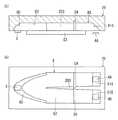
光学ブロック2は、合成樹脂成形体からなるカバー20の内部に導光体8が収納されて構成される。カバー20は、前後左右の長さ寸法がボディ10と等しい直方体形状に形成されるとともに下面側に開口する凹所200が設けられ、この凹所200内に導光体8を収納した状態でボディ10の上面側に接合される。また、カバー20上部の中央には、上下方向にカバー20を貫通する矩形の通気孔201が設けられ、通気孔201を通して外気(検出対象の気体を含む複数種類の混合気体。以下、同じ。)が凹所200(導光体8)内に導入される。なお、通気孔201の形状は矩形に限定されず、円形等の他の形状であってもよく、且つ複数個であってもよい。ただし、塵埃などの外気以外の異物が通気孔201に進入することを防ぐため、カバー20上面の通気孔201の開口は防塵フィルタ7で覆われている(図1参照)。 The optical block 2 is configured by housing a
導光体8は、図1に示すように第1反射鏡80と、第2反射鏡81と、第3反射鏡82と、第4反射鏡83とで構成される。第1反射鏡80は、例えば、放物面形状の反射面を有し、発光部3から放射される赤外線の光路(図1における破線参照)をボディ10の上面に沿った方向(左右方向)へ反射(変更)するものである。また第2反射鏡81は、例えば、平坦な反射面を有し、第1反射鏡80で変更された光路を受光部4の受光面(上面)と交差する方向(上下方向)へ反射(変更)するものである。また、第3反射鏡82は第1反射鏡80と第2反射鏡81が両端に配置された半円筒形状に形成されている。ただし、第3反射鏡82の中央部には、カバー20の通気孔201と繋がる孔(図示せず)が開口している。なお、これら3つの反射鏡80〜82は、金属材料で形成されてカバー20にインサート成形されてもよいし、あるいは、凹所200の内面にアルミニウムなどの金属が蒸着又はめっきされることで形成されてもよい。特に、反射鏡80〜82が蒸着やめっきによって形成される場合、金属材料で形成される場合と比較して、低コスト化と寸法精度の向上を図ることができる。 The
第4反射鏡83は、図2に示すようにアルミニウムなどの金属材料の板材で平板状に構成される、若しくは、成形品にアルミニウムなどの金属が蒸着又はめっきされることで平板状に形成されている。ボディ10の凹所100における前後両側の開口縁に、第4反射鏡83の厚み(上下方向の厚み)とほぼ等しい段差106が形成されており、反射面を上に向けた状態で第4反射鏡83の前後両側の端部が段差106上に載置される。つまり、図1に示すようにボディ10の壁102から上側凹部103までの範囲で、凹所100の開口が第4反射鏡83で塞がれることになる。このとき、第4反射鏡83の反射面(上面)が発光部3の発光面(上面)よりも低くなると信号処理回路部6や配線板11などが収納される凹所100の深さを深くしなければならないためにボディ10の厚み(高さ)が増してしまう。一方、第4反射鏡83の反射面が発光部3の発光面よりも高くなると第4反射鏡83の端部で赤外線が反射して損失が増えてしまうので、発光部3や受光部4のサイズを大きくする必要が生じて小型化が困難になる。これに対して本実施形態では、第4反射鏡83がその厚み寸法とほぼ等しい段差106に載置されることで第4反射鏡83の反射面が発光部3の発光面(上面)とが面一となっているので、上述のような不都合を回避することができる。 As shown in FIG. 2, the fourth reflecting
上述のように構成されるガスセンサでは、通気孔201を通して導光体8内に外気が導入され、発光部3から放射される赤外線が外気に含まれる検出対象の気体に吸収されることで受光部4の赤外線受光量が減少する。したがって、赤外線受光量に応じた受光部4の出力信号が信号処理回路部6で信号処理されることにより、導光体8内の外気に含まれる検出対象の気体(気体成分)の濃度が検出できる。ただし、気体濃度を検出するために信号処理回路部6で行われる信号処理の具体的な内容については、従来周知であるから詳細な説明は省略する。 In the gas sensor configured as described above, the outside air is introduced into the
而して、本実施形態では第1反射鏡80と第2反射鏡81によって赤外線の光路(図1の破線参照)が略コ字形に変更され、波長フィルタ5の赤外線の入射角(波長フィルタ5表面の法線方向との為す角。以下、同じ。)がほぼ零度となっている。このため、従来例に比べて波長フィルタ5の入射角依存性の影響を受け難くすることができ、その結果、波長フィルタ5を通過して受光部4に到達する赤外線量を増やすことができて気体成分の検出精度の低下を抑制することができる。また本実施形態では、光路が略V字形である特許文献2記載の従来例と比較して、光路長を短縮せずに上下方向の高さ寸法を小型化(低背化)することができる。しかも、低背化により、特許文献2記載の従来例と比較して通気孔201から光路までの距離が短縮されるので、外気中における検出対象気体の割合変化に対する検出応答性の向上が図れるという利点もある。さらに、発光部3及び受光部4がそれぞれ半導体ベアチップ(発光ダイオードチップ及びフォトダイオードチップ)で構成されているので、パッケージ型の発光ダイオードやフォトダイオードが使用される従来例に比べて配線の簡単化が図れる。 Thus, in the present embodiment, the first reflecting
また本実施形態では、発光部3と受光部4に挟まれ且つ第1反射鏡80で変更される光路と重ならない位置、すなわち、ボディ10の内部(凹所100内)に信号処理回路部6を配置することにより、デッドスペースを有効利用してボディ10及びカバー20の小型化を図っている。 In the present embodiment, the signal
ところで、カバー20の下面における左右方向の中央付近且つ前後方向の両端に、略円柱形状の突起202がそれぞれ下向きに突設されている(図4参照)。また、ボディ10の上面における左右方向の中央付近且つ前後方向の両端に、カバー20の突起202と嵌合する円形の嵌合孔107がそれぞれ設けられている(図2及び図3参照)。すなわち、突起202と嵌合孔107を嵌合させることでボディ10とカバー20の接合時の位置決めを可能とし、発光部3と第1反射鏡80との位置合わせ及び受光部4と第2反射鏡81との位置合わせを容易にしている。特に本実施形態では、第1反射鏡80の反射面が放物面形状に形成されており、ボディ10とカバー20が位置決めされることで反射面(放物面)の焦点の位置に発光部3を容易に配置することができる。 By the way, substantially
ここで、本実施形態が自動組立機によって組み立てられる場合、上方からカメラで撮像されるボディ10の画像から周知の画像処理技術(例えば、エッジ検出)を利用して、発光部3や受光部4の実装位置の位置決めが行われる。本実施形態では、図4に示すようにボディ10における嵌合孔107の底面に、嵌合孔107よりも小径の孔108が設けられ、この孔108の開口縁(エッジ)によって嵌合孔107の位置が検出され、嵌合孔107の位置を基準にして発光部3や受光部4の実装位置が位置決めされる。周知の画像処理技術を用いて嵌合穴107の開口縁によって嵌合穴107の位置検出を行った場合、発光部3や受光部4の表面の深さ方向の位置と嵌合穴107の深さ方向の位置が異なるため、撮像画像における結像(ピント)位置が異なることによる位置検出誤差が発生する。この位置検出誤差を低減するために小径の孔108を設け、その開口縁の深さ方向の位置が発光部3や受光部4の表面の深さ方向の位置に近づくようにしている。つまり、本実施形態では、回路ブロック1と光学ブロック2の位置決めと、ボディ10に対する発光部3及び受光部4の実装位置の位置決めとが同じ嵌合孔107を基準として行われる。その結果、双方の位置決めが異なる部位を基準とする場合に比較して、発光部3及び受光部4と導光体8(第1反射鏡80及び第2反射鏡81)との位置合わせの精度が向上するという利点がある。 Here, when the present embodiment is assembled by the automatic assembly machine, the
ところで、第1反射鏡80の大きさに対して発光部3が点光源とみなせる程度に小さくないため、発光部3から放射される赤外線の一部しか第1反射鏡80の反射面(放物面)の焦点を通らないことになる。そして、反射面の焦点を通らない赤外線の一部が波長フィルタ5の入射角範囲から外れ、受光部4に受光される赤外線量が減少してしまうことになる。そこで、図5に示すように発光部3と第1反射鏡80の間の光路上に集光用のレンズ21を配置し、レンズ21の集光点と第1反射鏡80の焦点を一致させることが好ましい。このようにすれば、発光部3から放射される赤外線の大部分が第1反射鏡80の焦点を通ることになるから、赤外線を効率よく受光部4に受光させることができる。 By the way, since the
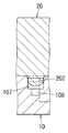
なお、本実施形態では波長フィルタ5がボディ10に取り付けられているが、図6に示すように波長フィルタ5が受光部4(半導体ベアチップ)に取り付けられても構わない。例えば、矩形平板状の波長フィルタ5が、受光部4の受光面40を覆うように受光部4の上面に接合される。ただし、波長フィルタ5下面の周縁に枠部50が設けられており、この枠部50によって受光部4の受光面40と波長フィルタ5の下面との間に隙間が形成されている。なお、下面が平坦である波長フィルタ5が、低融点ガラスや低融点金属、ポリマーなどの接合材51で接合されても構わない(図6(c)参照)。このように波長フィルタ5が受光部4と一体に構成されれば、波長フィルタ5を取り付けるための上側凹部103が不要となり、しかも、波長フィルタ5と受光面との間の隙間が小さくなるので、ボディ10の厚みを減らして小型化(低背化)が図れるという利点がある。さらに、多数の受光部4と波長フィルタ5が半導体ウェハの製造プロセスを利用して一括して製造可能となり、製造コストの削減が可能になる。あるいは、第1反射鏡80と第2反射鏡81の間に波長フィルタ5が設けられてもよい。 Although the
ここで、第1反射鏡80は反射面が放物面形状のものに限定されず、例えば、球面形状や多角形面形状の反射面を有するものであっても構わない。同様に、第2反射鏡81は反射面が平坦なものに限定されず、曲面形状の反射面を有するものであっても構わない。 Here, the first reflecting
(実施形態2)
本実施形態のガスセンサを図7に示す。本実施形態は、受光部4と波長フィルタ5の組を2組備える点に特徴があり、その他の構成については実施形態1と共通である。故に、実施形態1と共通の構成要素には同一の符号を付して適宜図示及び説明を省略する。(Embodiment 2)
The gas sensor of this embodiment is shown in FIG. The present embodiment is characterized in that two sets of the
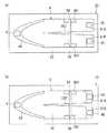
図7に示すように、ボディ10の上面側における右端部において、2つの下側凹部104A,104Bが前後方向に並べて形成される。そして、各下側凹部104A,104Bの底面に受光部4A,4Bがそれぞれ実装されるとともに、各受光部4A,4Bの上方を覆うようにそれぞれ波長フィルタ5A,5Bが上側凹部103の底面に配置される。 As shown in FIG. 7, at the right end portion on the upper surface side of the
ここで、一方の波長フィルタ(主波長フィルタ)5Aは、検出対象の気体が吸収する赤外線の波長域を通過域に含むが、他方の波長フィルタ(副波長フィルタ)5Bは、検出対象の気体が吸収する赤外線の波長域を通過域に含まず、当該波長域の近傍の波長域を通過域に含んでいる。つまり、発光部3から放射される赤外線のうち、主波長フィルタ5Aを通過して受光部4Aで受光される赤外線量が検出対象の気体の濃度に応じて減少するのに対し、副波長フィルタ5Bを通過して受光部4Bで受光される赤外線量は検出対象の気体の濃度に応じて減少しない。そして、信号処理回路部6では、2つの受光部4A,4Bの出力信号レベルの差分をとり、この差分に基づいて検出対象の気体の濃度を演算する。 Here, one wavelength filter (primary wavelength filter) 5A includes the infrared wavelength band absorbed by the gas to be detected in the pass band, while the other wavelength filter (sub-wavelength filter) 5B has the gas to be detected The wavelength range of infrared rays to be absorbed is not included in the passband, and the wavelength range near the wavelength range is included in the passband. That is, among the infrared rays radiated from the
すなわち、実施形態1のように受光部4の出力信号レベルに基づいて信号処理回路部6が気体濃度を演算した場合、受光部4の出力信号レベルが何らかの外乱要因によって変動したときに気体濃度の検出精度が低下してしまう虞がある。一方、上述のように信号処理回路部6が2つの受光部4A,4Bの出力信号レベルの差分に基づいて検出対象の気体の濃度を演算すれば、それぞれの受光部4の出力信号レベルの変動分を相殺して気体濃度の検出精度の低下を抑制することができる。 That is, when the signal
なお、図8に示すようにボディ10を立体配線基板(いわゆるMID基板)とすれば、信号処理回路部6が配線板11を介さずにボディ10に直接実装可能となるので、ボディ10をさらに小型化することができる。 If the
(実施形態3)
本実施形態のガスセンサを図9に示す。本実施形態は、光学ブロック2の構成に特徴があり、その他の構成については実施形態2と共通である。故に、実施形態2と共通の構成要素には同一の符号を付して適宜図示及び説明を省略する。(Embodiment 3)
The gas sensor of this embodiment is shown in FIG. The present embodiment is characterized by the configuration of the optical block 2, and the other configurations are the same as those of the second embodiment. Therefore, the same components as those in the second embodiment are denoted by the same reference numerals, and illustration and description thereof are omitted as appropriate.
本実施形態では、図9(b)に示すようにカバー20の凹所200底面より分岐部203が下向きに立設されている。この分岐部203は、先端(左端)が先細りとなった楔型の壁からなり、後端(右端)が2つの受光部4A,4Bの間に位置して第1反射鏡80で反射される赤外線の光路を2つの光路に分岐している(図9(a)参照)。また、分岐部203で分岐された各光路の途中に主波長フィルタ5A及び副波長フィルタ5Bが配設され、各光路の右端にそれぞれ第2反射鏡81A,81Bが配置されている。すなわち、一方の光路(主光路)を進行した赤外線が主波長フィルタ5Aを通過し且つ第2反射鏡81Aに反射されて受光部4Aに受光され、他方の光路(副光路)を進行した赤外線が副波長フィルタ5Bを通過し且つ第2反射鏡81Bに反射されて受光部4Bに受光される。 In the present embodiment, as shown in FIG. 9B, the branching
而して、実施形態2では導光体8内の光路が分岐されていないため、2つの受光部4A,4Bの受光面に対する赤外線の入射範囲(以下、スポットと呼ぶ。)が相対的に大きくなって、各受光部4A,4Bにおける赤外線の受光量が減少してしまう虞がある。これに対して本実施形態では、導光体8内の光路が分岐されているので、各受光部4A,4Bの受光面に対するスポットが相対的に小さくなり、その結果、各受光部4A,4Bにおける赤外線の受光量の減少を抑制することができる。 Thus, in the second embodiment, since the optical path in the
通気孔201は導光体8内に1つまたは複数設けられる。波長フィルタ5が第1反射鏡80と第2反射鏡81の間の光路上に設置される場合、波長フィルタ5よりも第1反射鏡80側と波長フィルタ5よりも第2反射鏡81側の両方、もしくは、両方にまたがるように通気孔201を設置することが望ましい。このようにすれば、被検出気体により赤外線が吸収されるための光路長を長くして気体の検出精度を高めることができる。さらに、光学シミュレーションにより、光路の端部における赤外線の通過量が少ないため、図10(a),(b)に示すように光路の両端に通気孔201が設けられることが望ましい。 One or more vent holes 201 are provided in the
ここで、図11に示すように第2反射鏡81A,81Bの反射面を曲面(凹曲面)とすれば、第2反射鏡81A,81Bの反射面で反射する光を集光させてスポットを縮小することができるので、各受光部4A,4Bにおける赤外線の受光量の減少をさらに抑制することができる。 Here, as shown in FIG. 11, if the reflecting surfaces of the second reflecting
(実施形態4)
実施形態1〜3では外気に含まれる1種類の気体の濃度を検出するガスセンサを例示した。これに対して本実施形態のガスセンサは、図12に示すように発光部3と受光部4と導光体8の組を複数組(図示例では2組)備え、それぞれの組毎に異なる種類の気体の濃度を検出することができる。(Embodiment 4)
In Embodiments 1-3, the gas sensor which detects the density | concentration of 1 type of gas contained in external air was illustrated. On the other hand, the gas sensor of this embodiment includes a plurality of sets (two sets in the illustrated example) of the
図12(a)に示すように、2つの発光部3と2つの受光部4がボディ(図示せず)に実装され、カバー20の凹所200には、各発光部3から放射される赤外線を各受光部4まで導光する2つの導光体8が並設されている。なお、これら2つの導光体8の構成は、第1反射鏡80と第2反射鏡81との間の光路上にそれぞれ波長フィルタ5が配置されている点を除いて実施形態1の導光体8と共通である。各波長フィルタ5はそれぞれの検出対象の気体の吸収特性に対応した波長を通過域に含むバンドパスフィルタからなる。 As shown in FIG. 12A, two light emitting
而して、本実施形態のガスセンサでは、外気に含まれる複数種類の気体から異なる2種類の気体(例えば、一酸化炭素と窒素酸化物など)の濃度をそれぞれ独立して検出することができる。なお、本実施形態においても、実施形態3と同様に第2反射鏡81の反射面を曲面(凹曲面)としてもよい。あるいは、実施形態3と同様に、各組毎に分岐部と2つの受光部4A,4Bと波長フィルタ5A,5Bを備え、各受光部4A,4Bの出力信号レベルの差分からそれぞれの気体の濃度を検出しても構わない。 Thus, the gas sensor of the present embodiment can independently detect the concentrations of two different types of gases (for example, carbon monoxide and nitrogen oxide) from a plurality of types of gases contained in the outside air. Also in this embodiment, the reflection surface of the second reflecting
3 発光部
4 受光部
5 波長フィルタ
8 導光体
10 ボディ(保持体)
80 第1反射鏡
81 第2反射鏡
82 第3反射鏡3
10 Body (holding body)
80 First reflector
81 Second reflector
82 Third reflector
Claims (18)
Translated fromJapanesePriority Applications (4)
| Application Number | Priority Date | Filing Date | Title |
|---|---|---|---|
| JP2011086891AJP5906407B2 (en) | 2011-04-11 | 2011-04-11 | Gas component detector |
| US14/110,999US9134224B2 (en) | 2011-04-11 | 2012-04-05 | Gas component detection device |
| PCT/IB2012/000693WO2012140485A1 (en) | 2011-04-11 | 2012-04-05 | Gas component detection device |
| TW101112541ATW201245692A (en) | 2011-04-11 | 2012-04-10 | Gaseous substance detecting apparatus |
Applications Claiming Priority (1)
| Application Number | Priority Date | Filing Date | Title |
|---|---|---|---|
| JP2011086891AJP5906407B2 (en) | 2011-04-11 | 2011-04-11 | Gas component detector |
Publications (2)
| Publication Number | Publication Date |
|---|---|
| JP2012220351A JP2012220351A (en) | 2012-11-12 |
| JP5906407B2true JP5906407B2 (en) | 2016-04-20 |
Family
ID=47008888
Family Applications (1)
| Application Number | Title | Priority Date | Filing Date |
|---|---|---|---|
| JP2011086891AExpired - Fee RelatedJP5906407B2 (en) | 2011-04-11 | 2011-04-11 | Gas component detector |
Country Status (4)
| Country | Link |
|---|---|
| US (1) | US9134224B2 (en) |
| JP (1) | JP5906407B2 (en) |
| TW (1) | TW201245692A (en) |
| WO (1) | WO2012140485A1 (en) |
Families Citing this family (35)
| Publication number | Priority date | Publication date | Assignee | Title |
|---|---|---|---|---|
| JP5985909B2 (en)* | 2012-07-10 | 2016-09-06 | 旭化成エレクトロニクス株式会社 | Gas sensor |
| US9113570B2 (en)* | 2012-10-31 | 2015-08-18 | Tyco Electronics Services Gmbh | Planar electronic device having a magnetic component |
| JP6029073B2 (en)* | 2012-11-30 | 2016-11-24 | パナソニックIpマネジメント株式会社 | Optical sensor device and method for manufacturing optical element used in optical sensor device |
| JP6347051B2 (en)* | 2013-03-04 | 2018-06-27 | パナソニックIpマネジメント株式会社 | device |
| CH709022A1 (en)* | 2013-12-23 | 2015-06-30 | Sauter Ag | Gas sensor. |
| TW201525442A (en)* | 2013-12-27 | 2015-07-01 | Lingsen Precision Ind Ltd | Gas sensor of miniature package structure and method of making the same |
| US20170023413A1 (en)* | 2014-04-22 | 2017-01-26 | Nec Corporation | Semiconductor device, infrared imaging device equipped with the semiconductor device, and method for controlling semiconductor device |
| JP6533719B2 (en)* | 2015-08-28 | 2019-06-19 | 旭化成エレクトロニクス株式会社 | Light emitting and receiving device |
| TWI580990B (en)* | 2015-12-27 | 2017-05-01 | 昇佳電子股份有限公司 | Sensing device and sensing device manufacturing method |
| WO2017204030A1 (en)* | 2016-05-25 | 2017-11-30 | パナソニックIpマネジメント株式会社 | Device |
| DE102016114542A1 (en)* | 2016-08-05 | 2018-02-08 | Osram Opto Semiconductors Gmbh | Detection arrangement and method for producing detection arrangements |
| WO2018066930A1 (en)* | 2016-10-06 | 2018-04-12 | 주식회사 템퍼스 | Integrated gas sensor structure and infrared light emitting module |
| US10161859B2 (en) | 2016-10-27 | 2018-12-25 | Honeywell International Inc. | Planar reflective ring |
| EP3144663B1 (en) | 2016-11-18 | 2020-06-17 | Sensirion AG | Gas sensor module |
| WO2018097071A1 (en)* | 2016-11-28 | 2018-05-31 | 京セラ株式会社 | Sensor wiring board, sensor package, and sensor device |
| KR102643353B1 (en)* | 2016-12-06 | 2024-03-07 | 엘지전자 주식회사 | gas sensor |
| DE102017208463A1 (en)* | 2017-05-18 | 2018-11-22 | Robert Bosch Gmbh | Optical sensor |
| DE212018000235U1 (en)* | 2017-05-30 | 2020-01-07 | Analog Devices, Inc. | Compact optical gas detection system and device |
| EP3421947B1 (en) | 2017-06-30 | 2019-08-07 | Sensirion AG | Operation method for flow sensor device |
| US11788942B2 (en) | 2017-12-15 | 2023-10-17 | Analog Devices, Inc. | Compact optical smoke detector system and apparatus |
| KR20200034564A (en)* | 2018-09-20 | 2020-03-31 | 주식회사 제우스 | Flow cell apparatus |
| US11073467B2 (en) | 2018-09-28 | 2021-07-27 | Stmicroelectronics S.R.L. | Miniaturized optical particle detector |
| US11079321B2 (en)* | 2018-09-28 | 2021-08-03 | Stmicroelectronics S.R.L. | NDIR detector device for detecting gases having an infrared absorption spectrum |
| US12211370B2 (en) | 2018-12-02 | 2025-01-28 | Analog Devices, Inc. | Fire detection system |
| US10663394B1 (en) | 2019-01-03 | 2020-05-26 | Advanced Semiconductor Engineering, Inc. | Optical devices for sensing gas |
| CN111721730A (en)* | 2019-03-20 | 2020-09-29 | 中国科学院半导体研究所 | Non-spectroscopic infrared gas sensor |
| US11796445B2 (en) | 2019-05-15 | 2023-10-24 | Analog Devices, Inc. | Optical improvements to compact smoke detectors, systems and apparatus |
| USD913135S1 (en) | 2019-05-15 | 2021-03-16 | Analog Devices, Inc. | Smoke chamber blocking ensemble |
| US11747272B2 (en) | 2019-06-10 | 2023-09-05 | Analog Devices, Inc. | Gas detection using differential path length measurement |
| CN115362097A (en)* | 2020-04-15 | 2022-11-18 | 上海延锋金桥汽车饰件系统有限公司 | vehicle interior parts |
| US11821836B2 (en) | 2020-07-13 | 2023-11-21 | Analog Devices, Inc. | Fully compensated optical gas sensing system and apparatus |
| US11747273B2 (en)* | 2020-09-28 | 2023-09-05 | Asahi Kasei Microdevices Corporation | Gas sensor |
| GB2628672A (en)* | 2023-03-31 | 2024-10-02 | Servomex Group Ltd | Method, apparatus and system for compact optical gas absorption measurements |
| CN117147441B (en)* | 2023-07-18 | 2024-04-12 | 镭友芯科技(苏州)有限公司 | A gas detector and a method for preparing the same |
| US20250216327A1 (en)* | 2023-12-28 | 2025-07-03 | Renesas Electronics America Inc. | Compact injection molded optical module for gas sensing |
Family Cites Families (18)
| Publication number | Priority date | Publication date | Assignee | Title |
|---|---|---|---|---|
| JPH0684937B2 (en)* | 1987-07-08 | 1994-10-26 | 株式会社日立製作所 | Light absorbing gas sensor |
| US5747808A (en)* | 1994-02-14 | 1998-05-05 | Engelhard Sensor Technologies | NDIR gas sensor |
| JPH0924799A (en)* | 1995-05-11 | 1997-01-28 | Omron Corp | Vehicle with precipitation particle detection sensor |
| JPH09184803A (en) | 1995-12-29 | 1997-07-15 | Horiba Ltd | Infrared gas analyzer |
| US6067840A (en) | 1997-08-04 | 2000-05-30 | Texas Instruments Incorporated | Method and apparatus for infrared sensing of gas |
| US6410918B1 (en)* | 1997-10-28 | 2002-06-25 | Edwards Systems Technology, Inc. | Diffusion-type NDIR gas analyzer with improved response time due to convection flow |
| US6396056B1 (en)* | 1999-07-08 | 2002-05-28 | Air Instruments And Measurements, Inc. | Gas detectors and gas analyzers utilizing spectral absorption |
| JP2001153801A (en)* | 1999-11-25 | 2001-06-08 | Matsushita Electric Works Ltd | Photoelectric particle detection sensor |
| JP2002352347A (en)* | 2001-05-28 | 2002-12-06 | Matsushita Electric Works Ltd | Fire sensor |
| JP2002350341A (en)* | 2001-05-25 | 2002-12-04 | Nok Corp | Carbon monoxide concentration detecting apparatus |
| JP2003248877A (en)* | 2002-02-25 | 2003-09-05 | Matsushita Electric Works Ltd | Smoke sensor |
| DE10360215A1 (en)* | 2003-12-20 | 2005-07-28 | Robert Bosch Gmbh | gas sensor |
| DE102004007946A1 (en) | 2004-02-18 | 2005-09-15 | Tyco Electronics Raychem Gmbh | Gas sensor arrangement in integrated design |
| JP2006003233A (en) | 2004-06-17 | 2006-01-05 | Otsuka Denshi Co Ltd | Optical cell measuring device |
| DE102004031316B3 (en)* | 2004-06-29 | 2005-12-29 | Robert Bosch Gmbh | Gas sensor module for the spectroscopic measurement of a gas concentration |
| DE102004044145B3 (en)* | 2004-09-13 | 2006-04-13 | Robert Bosch Gmbh | Reflector module for a photometric gas sensor |
| JP2006275980A (en) | 2005-03-30 | 2006-10-12 | Denso Corp | Infrared-type gas detector |
| JP2006300738A (en)* | 2005-04-21 | 2006-11-02 | Matsushita Electric Works Ltd | Gas sensor |
- 2011
- 2011-04-11JPJP2011086891Apatent/JP5906407B2/ennot_activeExpired - Fee Related
- 2012
- 2012-04-05USUS14/110,999patent/US9134224B2/enactiveActive
- 2012-04-05WOPCT/IB2012/000693patent/WO2012140485A1/enactiveApplication Filing
- 2012-04-10TWTW101112541Apatent/TW201245692A/enunknown
Also Published As
| Publication number | Publication date |
|---|---|
| US20140070101A1 (en) | 2014-03-13 |
| JP2012220351A (en) | 2012-11-12 |
| US9134224B2 (en) | 2015-09-15 |
| TW201245692A (en) | 2012-11-16 |
| WO2012140485A1 (en) | 2012-10-18 |
Similar Documents
| Publication | Publication Date | Title |
|---|---|---|
| JP5906407B2 (en) | Gas component detector | |
| JP6347051B2 (en) | device | |
| JP6530652B2 (en) | Light emitting and receiving device | |
| JPH11118711A (en) | Method for indicating gas concentration and gas sensor device | |
| US11073636B2 (en) | Optical detection assembly | |
| TWI513974B (en) | Detector | |
| JP2012220352A (en) | Gas component detector | |
| JP2012220353A (en) | Gas component detection apparatus | |
| WO2019176284A1 (en) | Limited-reflection-type sensor | |
| JP2012215396A (en) | Infrared gas sensor | |
| JP2013120156A (en) | Gas component detector | |
| JP2013120155A (en) | Gas component detector | |
| JP2013120154A (en) | Gas component detector | |
| JP7602934B2 (en) | Gas detection equipment | |
| JP2020041935A (en) | Toner deposition amount sensor | |
| CN114965339A (en) | Integrated infrared gas sensor with special-shaped gas chamber and using method thereof | |
| US20240310276A1 (en) | Optical concentration measuring apparatus | |
| US20250216327A1 (en) | Compact injection molded optical module for gas sensing | |
| US12411079B2 (en) | Gas detection apparatus | |
| WO2006016504A1 (en) | Optical device for photoelectric sensor and photoelectric sensor using the same | |
| US20240295493A1 (en) | Optical physical quantity measuring apparatus | |
| US11474031B2 (en) | Gas detection apparatus | |
| WO2011158540A1 (en) | Color sensor | |
| KR102265045B1 (en) | Optical gas sensor | |
| US20230349814A1 (en) | Gas detection device |
Legal Events
| Date | Code | Title | Description |
|---|---|---|---|
| A621 | Written request for application examination | Free format text:JAPANESE INTERMEDIATE CODE: A621 Effective date:20140224 | |
| A711 | Notification of change in applicant | Free format text:JAPANESE INTERMEDIATE CODE: A711 Effective date:20141008 | |
| A131 | Notification of reasons for refusal | Free format text:JAPANESE INTERMEDIATE CODE: A131 Effective date:20150217 | |
| A521 | Request for written amendment filed | Free format text:JAPANESE INTERMEDIATE CODE: A523 Effective date:20150420 | |
| A131 | Notification of reasons for refusal | Free format text:JAPANESE INTERMEDIATE CODE: A131 Effective date:20150908 | |
| A521 | Request for written amendment filed | Free format text:JAPANESE INTERMEDIATE CODE: A523 Effective date:20151109 | |
| TRDD | Decision of grant or rejection written | ||
| A01 | Written decision to grant a patent or to grant a registration (utility model) | Free format text:JAPANESE INTERMEDIATE CODE: A01 Effective date:20151208 | |
| A61 | First payment of annual fees (during grant procedure) | Free format text:JAPANESE INTERMEDIATE CODE: A61 Effective date:20160106 | |
| R151 | Written notification of patent or utility model registration | Ref document number:5906407 Country of ref document:JP Free format text:JAPANESE INTERMEDIATE CODE: R151 | |
| LAPS | Cancellation because of no payment of annual fees |