JP5905060B1 - Additive manufacturing apparatus and additive manufacturing method - Google Patents
Additive manufacturing apparatus and additive manufacturing methodDownload PDFInfo
- Publication number
- JP5905060B1 JP5905060B1JP2014187982AJP2014187982AJP5905060B1JP 5905060 B1JP5905060 B1JP 5905060B1JP 2014187982 AJP2014187982 AJP 2014187982AJP 2014187982 AJP2014187982 AJP 2014187982AJP 5905060 B1JP5905060 B1JP 5905060B1
- Authority
- JP
- Japan
- Prior art keywords
- laser beam
- unit
- laser
- additive manufacturing
- elastic wave
- Prior art date
- Legal status (The legal status is an assumption and is not a legal conclusion. Google has not performed a legal analysis and makes no representation as to the accuracy of the status listed.)
- Expired - Fee Related
Links
Images


Classifications
- G—PHYSICS
- G01—MEASURING; TESTING
- G01N—INVESTIGATING OR ANALYSING MATERIALS BY DETERMINING THEIR CHEMICAL OR PHYSICAL PROPERTIES
- G01N29/00—Investigating or analysing materials by the use of ultrasonic, sonic or infrasonic waves; Visualisation of the interior of objects by transmitting ultrasonic or sonic waves through the object
- G01N29/04—Analysing solids
- G01N29/043—Analysing solids in the interior, e.g. by shear waves
- B—PERFORMING OPERATIONS; TRANSPORTING
- B22—CASTING; POWDER METALLURGY
- B22F—WORKING METALLIC POWDER; MANUFACTURE OF ARTICLES FROM METALLIC POWDER; MAKING METALLIC POWDER; APPARATUS OR DEVICES SPECIALLY ADAPTED FOR METALLIC POWDER
- B22F10/00—Additive manufacturing of workpieces or articles from metallic powder
- B22F10/20—Direct sintering or melting
- B22F10/25—Direct deposition of metal particles, e.g. direct metal deposition [DMD] or laser engineered net shaping [LENS]
- B—PERFORMING OPERATIONS; TRANSPORTING
- B22—CASTING; POWDER METALLURGY
- B22F—WORKING METALLIC POWDER; MANUFACTURE OF ARTICLES FROM METALLIC POWDER; MAKING METALLIC POWDER; APPARATUS OR DEVICES SPECIALLY ADAPTED FOR METALLIC POWDER
- B22F10/00—Additive manufacturing of workpieces or articles from metallic powder
- B22F10/30—Process control
- B22F10/36—Process control of energy beam parameters
- B—PERFORMING OPERATIONS; TRANSPORTING
- B22—CASTING; POWDER METALLURGY
- B22F—WORKING METALLIC POWDER; MANUFACTURE OF ARTICLES FROM METALLIC POWDER; MAKING METALLIC POWDER; APPARATUS OR DEVICES SPECIALLY ADAPTED FOR METALLIC POWDER
- B22F10/00—Additive manufacturing of workpieces or articles from metallic powder
- B22F10/30—Process control
- B22F10/38—Process control to achieve specific product aspects, e.g. surface smoothness, density, porosity or hollow structures
- B—PERFORMING OPERATIONS; TRANSPORTING
- B22—CASTING; POWDER METALLURGY
- B22F—WORKING METALLIC POWDER; MANUFACTURE OF ARTICLES FROM METALLIC POWDER; MAKING METALLIC POWDER; APPARATUS OR DEVICES SPECIALLY ADAPTED FOR METALLIC POWDER
- B22F10/00—Additive manufacturing of workpieces or articles from metallic powder
- B22F10/50—Treatment of workpieces or articles during build-up, e.g. treatments applied to fused layers during build-up
- B—PERFORMING OPERATIONS; TRANSPORTING
- B22—CASTING; POWDER METALLURGY
- B22F—WORKING METALLIC POWDER; MANUFACTURE OF ARTICLES FROM METALLIC POWDER; MAKING METALLIC POWDER; APPARATUS OR DEVICES SPECIALLY ADAPTED FOR METALLIC POWDER
- B22F10/00—Additive manufacturing of workpieces or articles from metallic powder
- B22F10/60—Treatment of workpieces or articles after build-up
- B22F10/66—Treatment of workpieces or articles after build-up by mechanical means
- B—PERFORMING OPERATIONS; TRANSPORTING
- B22—CASTING; POWDER METALLURGY
- B22F—WORKING METALLIC POWDER; MANUFACTURE OF ARTICLES FROM METALLIC POWDER; MAKING METALLIC POWDER; APPARATUS OR DEVICES SPECIALLY ADAPTED FOR METALLIC POWDER
- B22F10/00—Additive manufacturing of workpieces or articles from metallic powder
- B22F10/80—Data acquisition or data processing
- B22F10/85—Data acquisition or data processing for controlling or regulating additive manufacturing processes
- B—PERFORMING OPERATIONS; TRANSPORTING
- B22—CASTING; POWDER METALLURGY
- B22F—WORKING METALLIC POWDER; MANUFACTURE OF ARTICLES FROM METALLIC POWDER; MAKING METALLIC POWDER; APPARATUS OR DEVICES SPECIALLY ADAPTED FOR METALLIC POWDER
- B22F12/00—Apparatus or devices specially adapted for additive manufacturing; Auxiliary means for additive manufacturing; Combinations of additive manufacturing apparatus or devices with other processing apparatus or devices
- B22F12/40—Radiation means
- B22F12/44—Radiation means characterised by the configuration of the radiation means
- B—PERFORMING OPERATIONS; TRANSPORTING
- B22—CASTING; POWDER METALLURGY
- B22F—WORKING METALLIC POWDER; MANUFACTURE OF ARTICLES FROM METALLIC POWDER; MAKING METALLIC POWDER; APPARATUS OR DEVICES SPECIALLY ADAPTED FOR METALLIC POWDER
- B22F12/00—Apparatus or devices specially adapted for additive manufacturing; Auxiliary means for additive manufacturing; Combinations of additive manufacturing apparatus or devices with other processing apparatus or devices
- B22F12/90—Means for process control, e.g. cameras or sensors
- B—PERFORMING OPERATIONS; TRANSPORTING
- B29—WORKING OF PLASTICS; WORKING OF SUBSTANCES IN A PLASTIC STATE IN GENERAL
- B29C—SHAPING OR JOINING OF PLASTICS; SHAPING OF MATERIAL IN A PLASTIC STATE, NOT OTHERWISE PROVIDED FOR; AFTER-TREATMENT OF THE SHAPED PRODUCTS, e.g. REPAIRING
- B29C64/00—Additive manufacturing, i.e. manufacturing of three-dimensional [3D] objects by additive deposition, additive agglomeration or additive layering, e.g. by 3D printing, stereolithography or selective laser sintering
- B29C64/10—Processes of additive manufacturing
- B29C64/141—Processes of additive manufacturing using only solid materials
- B29C64/153—Processes of additive manufacturing using only solid materials using layers of powder being selectively joined, e.g. by selective laser sintering or melting
- B—PERFORMING OPERATIONS; TRANSPORTING
- B29—WORKING OF PLASTICS; WORKING OF SUBSTANCES IN A PLASTIC STATE IN GENERAL
- B29C—SHAPING OR JOINING OF PLASTICS; SHAPING OF MATERIAL IN A PLASTIC STATE, NOT OTHERWISE PROVIDED FOR; AFTER-TREATMENT OF THE SHAPED PRODUCTS, e.g. REPAIRING
- B29C64/00—Additive manufacturing, i.e. manufacturing of three-dimensional [3D] objects by additive deposition, additive agglomeration or additive layering, e.g. by 3D printing, stereolithography or selective laser sintering
- B29C64/10—Processes of additive manufacturing
- B29C64/188—Processes of additive manufacturing involving additional operations performed on the added layers, e.g. smoothing, grinding or thickness control
- B—PERFORMING OPERATIONS; TRANSPORTING
- B29—WORKING OF PLASTICS; WORKING OF SUBSTANCES IN A PLASTIC STATE IN GENERAL
- B29C—SHAPING OR JOINING OF PLASTICS; SHAPING OF MATERIAL IN A PLASTIC STATE, NOT OTHERWISE PROVIDED FOR; AFTER-TREATMENT OF THE SHAPED PRODUCTS, e.g. REPAIRING
- B29C64/00—Additive manufacturing, i.e. manufacturing of three-dimensional [3D] objects by additive deposition, additive agglomeration or additive layering, e.g. by 3D printing, stereolithography or selective laser sintering
- B29C64/30—Auxiliary operations or equipment
- B29C64/386—Data acquisition or data processing for additive manufacturing
- B—PERFORMING OPERATIONS; TRANSPORTING
- B29—WORKING OF PLASTICS; WORKING OF SUBSTANCES IN A PLASTIC STATE IN GENERAL
- B29C—SHAPING OR JOINING OF PLASTICS; SHAPING OF MATERIAL IN A PLASTIC STATE, NOT OTHERWISE PROVIDED FOR; AFTER-TREATMENT OF THE SHAPED PRODUCTS, e.g. REPAIRING
- B29C67/00—Shaping techniques not covered by groups B29C39/00 - B29C65/00, B29C70/00 or B29C73/00
- B—PERFORMING OPERATIONS; TRANSPORTING
- B33—ADDITIVE MANUFACTURING TECHNOLOGY
- B33Y—ADDITIVE MANUFACTURING, i.e. MANUFACTURING OF THREE-DIMENSIONAL [3-D] OBJECTS BY ADDITIVE DEPOSITION, ADDITIVE AGGLOMERATION OR ADDITIVE LAYERING, e.g. BY 3-D PRINTING, STEREOLITHOGRAPHY OR SELECTIVE LASER SINTERING
- B33Y10/00—Processes of additive manufacturing
- B—PERFORMING OPERATIONS; TRANSPORTING
- B33—ADDITIVE MANUFACTURING TECHNOLOGY
- B33Y—ADDITIVE MANUFACTURING, i.e. MANUFACTURING OF THREE-DIMENSIONAL [3-D] OBJECTS BY ADDITIVE DEPOSITION, ADDITIVE AGGLOMERATION OR ADDITIVE LAYERING, e.g. BY 3-D PRINTING, STEREOLITHOGRAPHY OR SELECTIVE LASER SINTERING
- B33Y30/00—Apparatus for additive manufacturing; Details thereof or accessories therefor
- B—PERFORMING OPERATIONS; TRANSPORTING
- B33—ADDITIVE MANUFACTURING TECHNOLOGY
- B33Y—ADDITIVE MANUFACTURING, i.e. MANUFACTURING OF THREE-DIMENSIONAL [3-D] OBJECTS BY ADDITIVE DEPOSITION, ADDITIVE AGGLOMERATION OR ADDITIVE LAYERING, e.g. BY 3-D PRINTING, STEREOLITHOGRAPHY OR SELECTIVE LASER SINTERING
- B33Y50/00—Data acquisition or data processing for additive manufacturing
- B33Y50/02—Data acquisition or data processing for additive manufacturing for controlling or regulating additive manufacturing processes
- G—PHYSICS
- G01—MEASURING; TESTING
- G01B—MEASURING LENGTH, THICKNESS OR SIMILAR LINEAR DIMENSIONS; MEASURING ANGLES; MEASURING AREAS; MEASURING IRREGULARITIES OF SURFACES OR CONTOURS
- G01B11/00—Measuring arrangements characterised by the use of optical techniques
- G01B11/24—Measuring arrangements characterised by the use of optical techniques for measuring contours or curvatures
- G01B11/2441—Measuring arrangements characterised by the use of optical techniques for measuring contours or curvatures using interferometry
- G—PHYSICS
- G01—MEASURING; TESTING
- G01N—INVESTIGATING OR ANALYSING MATERIALS BY DETERMINING THEIR CHEMICAL OR PHYSICAL PROPERTIES
- G01N21/00—Investigating or analysing materials by the use of optical means, i.e. using sub-millimetre waves, infrared, visible or ultraviolet light
- G01N21/17—Systems in which incident light is modified in accordance with the properties of the material investigated
- G01N21/1702—Systems in which incident light is modified in accordance with the properties of the material investigated with opto-acoustic detection, e.g. for gases or analysing solids
- G—PHYSICS
- G01—MEASURING; TESTING
- G01N—INVESTIGATING OR ANALYSING MATERIALS BY DETERMINING THEIR CHEMICAL OR PHYSICAL PROPERTIES
- G01N21/00—Investigating or analysing materials by the use of optical means, i.e. using sub-millimetre waves, infrared, visible or ultraviolet light
- G01N21/17—Systems in which incident light is modified in accordance with the properties of the material investigated
- G01N21/1717—Systems in which incident light is modified in accordance with the properties of the material investigated with a modulation of one or more physical properties of the sample during the optical investigation, e.g. electro-reflectance
- G—PHYSICS
- G01—MEASURING; TESTING
- G01N—INVESTIGATING OR ANALYSING MATERIALS BY DETERMINING THEIR CHEMICAL OR PHYSICAL PROPERTIES
- G01N29/00—Investigating or analysing materials by the use of ultrasonic, sonic or infrasonic waves; Visualisation of the interior of objects by transmitting ultrasonic or sonic waves through the object
- G01N29/22—Details, e.g. general constructional or apparatus details
- G01N29/24—Probes
- G01N29/2418—Probes using optoacoustic interaction with the material, e.g. laser radiation, photoacoustics
- B—PERFORMING OPERATIONS; TRANSPORTING
- B22—CASTING; POWDER METALLURGY
- B22F—WORKING METALLIC POWDER; MANUFACTURE OF ARTICLES FROM METALLIC POWDER; MAKING METALLIC POWDER; APPARATUS OR DEVICES SPECIALLY ADAPTED FOR METALLIC POWDER
- B22F12/00—Apparatus or devices specially adapted for additive manufacturing; Auxiliary means for additive manufacturing; Combinations of additive manufacturing apparatus or devices with other processing apparatus or devices
- B22F12/30—Platforms or substrates
- B22F12/33—Platforms or substrates translatory in the deposition plane
- B—PERFORMING OPERATIONS; TRANSPORTING
- B22—CASTING; POWDER METALLURGY
- B22F—WORKING METALLIC POWDER; MANUFACTURE OF ARTICLES FROM METALLIC POWDER; MAKING METALLIC POWDER; APPARATUS OR DEVICES SPECIALLY ADAPTED FOR METALLIC POWDER
- B22F12/00—Apparatus or devices specially adapted for additive manufacturing; Auxiliary means for additive manufacturing; Combinations of additive manufacturing apparatus or devices with other processing apparatus or devices
- B22F12/50—Means for feeding of material, e.g. heads
- B22F12/53—Nozzles
- B—PERFORMING OPERATIONS; TRANSPORTING
- B22—CASTING; POWDER METALLURGY
- B22F—WORKING METALLIC POWDER; MANUFACTURE OF ARTICLES FROM METALLIC POWDER; MAKING METALLIC POWDER; APPARATUS OR DEVICES SPECIALLY ADAPTED FOR METALLIC POWDER
- B22F12/00—Apparatus or devices specially adapted for additive manufacturing; Auxiliary means for additive manufacturing; Combinations of additive manufacturing apparatus or devices with other processing apparatus or devices
- B22F12/70—Gas flow means
- B—PERFORMING OPERATIONS; TRANSPORTING
- B29—WORKING OF PLASTICS; WORKING OF SUBSTANCES IN A PLASTIC STATE IN GENERAL
- B29K—INDEXING SCHEME ASSOCIATED WITH SUBCLASSES B29B, B29C OR B29D, RELATING TO MOULDING MATERIALS OR TO MATERIALS FOR MOULDS, REINFORCEMENTS, FILLERS OR PREFORMED PARTS, e.g. INSERTS
- B29K2105/00—Condition, form or state of moulded material or of the material to be shaped
- B29K2105/25—Solid
- B29K2105/251—Particles, powder or granules
- G—PHYSICS
- G01—MEASURING; TESTING
- G01N—INVESTIGATING OR ANALYSING MATERIALS BY DETERMINING THEIR CHEMICAL OR PHYSICAL PROPERTIES
- G01N21/00—Investigating or analysing materials by the use of optical means, i.e. using sub-millimetre waves, infrared, visible or ultraviolet light
- G01N21/17—Systems in which incident light is modified in accordance with the properties of the material investigated
- G01N21/1702—Systems in which incident light is modified in accordance with the properties of the material investigated with opto-acoustic detection, e.g. for gases or analysing solids
- G01N2021/1706—Systems in which incident light is modified in accordance with the properties of the material investigated with opto-acoustic detection, e.g. for gases or analysing solids in solids
- G—PHYSICS
- G01—MEASURING; TESTING
- G01N—INVESTIGATING OR ANALYSING MATERIALS BY DETERMINING THEIR CHEMICAL OR PHYSICAL PROPERTIES
- G01N2291/00—Indexing codes associated with group G01N29/00
- G01N2291/02—Indexing codes associated with the analysed material
- G01N2291/028—Material parameters
- G01N2291/0289—Internal structure, e.g. defects, grain size, texture
- G—PHYSICS
- G01—MEASURING; TESTING
- G01N—INVESTIGATING OR ANALYSING MATERIALS BY DETERMINING THEIR CHEMICAL OR PHYSICAL PROPERTIES
- G01N2291/00—Indexing codes associated with group G01N29/00
- G01N2291/26—Scanned objects
- G01N2291/267—Welds
- G—PHYSICS
- G01—MEASURING; TESTING
- G01N—INVESTIGATING OR ANALYSING MATERIALS BY DETERMINING THEIR CHEMICAL OR PHYSICAL PROPERTIES
- G01N2291/00—Indexing codes associated with group G01N29/00
- G01N2291/26—Scanned objects
- G01N2291/269—Various geometry objects
- G01N2291/2698—Other discrete objects, e.g. bricks
- Y—GENERAL TAGGING OF NEW TECHNOLOGICAL DEVELOPMENTS; GENERAL TAGGING OF CROSS-SECTIONAL TECHNOLOGIES SPANNING OVER SEVERAL SECTIONS OF THE IPC; TECHNICAL SUBJECTS COVERED BY FORMER USPC CROSS-REFERENCE ART COLLECTIONS [XRACs] AND DIGESTS
- Y02—TECHNOLOGIES OR APPLICATIONS FOR MITIGATION OR ADAPTATION AGAINST CLIMATE CHANGE
- Y02P—CLIMATE CHANGE MITIGATION TECHNOLOGIES IN THE PRODUCTION OR PROCESSING OF GOODS
- Y02P10/00—Technologies related to metal processing
- Y02P10/25—Process efficiency
Landscapes
- Chemical & Material Sciences (AREA)
- Engineering & Computer Science (AREA)
- Materials Engineering (AREA)
- Manufacturing & Machinery (AREA)
- Physics & Mathematics (AREA)
- Health & Medical Sciences (AREA)
- General Health & Medical Sciences (AREA)
- Analytical Chemistry (AREA)
- Optics & Photonics (AREA)
- General Physics & Mathematics (AREA)
- Pathology (AREA)
- Immunology (AREA)
- Biochemistry (AREA)
- Life Sciences & Earth Sciences (AREA)
- Mechanical Engineering (AREA)
- Automation & Control Theory (AREA)
- Toxicology (AREA)
- Acoustics & Sound (AREA)
- Length Measuring Devices By Optical Means (AREA)
- Powder Metallurgy (AREA)
- Laser Beam Processing (AREA)
Abstract
Translated fromJapaneseDescription
Translated fromJapanese本発明の実施形態は、積層造形装置および積層造形方法に関する。 Embodiments described herein relate generally to an additive manufacturing apparatus and an additive manufacturing method.
従来、積層造形物を造形する積層造形装置が知られている。積層造形装置は、粉末状の材料をレーザ光によって溶融させて層を形成し、当該層を積層することにより三次元形状の積層造形物を造形する。 Conventionally, an additive manufacturing apparatus for forming an additive manufacturing object is known. The additive manufacturing apparatus forms a layer by melting a powdery material with laser light, and forms a three-dimensional additive object by stacking the layers.
この種の積層造形装置によって造形される造形物の内部には、造形途中に生じた気泡等の異常領域が含まれる場合がある。このような造形物の内部の異常を検出できる積層造形装置および積層造形方法が得られれば有意義である。 There are cases where an abnormal region such as a bubble generated during modeling is included in a modeled object modeled by this type of additive manufacturing apparatus. It would be meaningful if an additive manufacturing apparatus and additive manufacturing method capable of detecting such abnormalities inside the object are obtained.
実施形態の積層造形装置は、造形部と、加工部と、弾性波検出部と、検査部と、を備える。前記造形部は、材料に第一のエネルギ線を照射して前記材料を固化させて形成する層を、順次積層する。前記加工部は、第二のエネルギ線の照射によって、前記層によって構成された造形物の表面を加工するとともに前記造形物の内部を伝播する弾性波を発生させる。前記弾性波検出部は、前記弾性波を検出する。前記検査部は、前記弾性波検出部の検出結果に基づいて、前記造形物を検査する。The additive manufacturing apparatus according to the embodiment includes a modeling unit, aprocessing unit , an elastic wave detection unit, and an inspection unit. The modeling unit sequentially stacks layers formed by irradiating the material with a first energy ray to solidify the material. The saidprocess part produces| generates the elastic wave which propagatesthe inside of thesaid molded article while processing thesurface of the molded article comprisedby the said layer byirradiation of a 2nd energy ray . The elastic wave detection unit detects the elastic wave. The inspection unit inspects the modeled object based on a detection result of the elastic wave detection unit.
以下、図面を参照して、実施形態について詳細に説明する。なお、以下の複数の実施形態には、同様の構成要素が含まれている。よって、以下では、それら同様の構成要素には共通の符号が付与されるとともに、重複する説明が省略される。 Hereinafter, embodiments will be described in detail with reference to the drawings. Note that similar components are included in the following embodiments. Therefore, below, the same code | symbol is provided to those similar components, and the overlapping description is abbreviate | omitted.
(第1の実施形態)
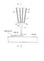
図1に示される本実施形態の積層造形装置1は、レーザデポジション方式で積層造形物を造形する。積層造形装置1は、処理槽11や、ステージ12、移動装置13、ノズル装置14、光学装置15、検査装置16、制御部17等を備えている。積層造形装置1は、ノズル装置14によって材料121(造形用材料)を供給するとともに当該材料121にレーザ光L1を照射することにより、ステージ12上に配置された対象物110に材料121の層110bを形成し、当該層110bを積層することにより積層造形物100を造形する。ここで、一つ以上の層110bによって造形物101が構成される。造形物101は、積層造形物100の造形過程の中間物や、造形が完成した積層造形物100である。(First embodiment)
The
対象物110は、ノズル装置14によって材料121が供給される対象であって、ベース110aおよび層110bを含む。複数の層110bがベース110aの上面に積層される。材料121は、粉末状の金属材料や樹脂材料等である。あるいは、材料121は、粉末状ではなく、線材であってもよい。造形には、一つ以上の材料121が用いられうる。 The
処理槽11には、主室21と副室22とが設けられている。副室22は、主室21と隣接して設けられている。主室21と副室22との間には扉部23が設けられている。扉部23が開かれた場合、主室21と副室22とが連通され、扉部23が閉じられた場合、主室21が気密状態になる。 The
主室21には、給気口21aおよび排気口21bが設けられている。給気装置(図示されず)の動作により、主室21内に給気口21aを介して窒素やアルゴン等の不活性ガスが供給される。排気装置(図示されず)の動作により、主室21から排気口21bを介して主室21内のガスが排出される。 The
また、主室21内には、移送装置(図示されず)が設けられている。また、主室21から副室22にかけて、搬送装置24が設けられている。移送装置は、主室21で処理された積層造形物100を、搬送装置24に渡す。搬送装置24は、移送装置から渡された積層造形物100を副室22内に搬送する。すなわち、副室22には、主室21で処理された積層造形物100が収容される。積層造形物100が副室22に収容された後、扉部23が閉じられ、副室22と主室21とが隔絶される。 Further, a transfer device (not shown) is provided in the
主室21内には、ステージ12や、移動装置13、ノズル装置14の一部、検査装置16等が設けられている。 In the
ステージ12は、対象物110を支持する。移動装置13は、ステージ12を、互いに直交する三軸方向に移動させることができる。 The
ノズル装置14は、ステージ12上に位置された対象物110に粉末状(あるいは線状)の材料121を供給する。また、ノズル装置14のノズル33は、ステージ12上に位置された対象物110にレーザ光L1を照射する。また、ノズル33は、材料121の供給と並行してレーザ光L1を照射する。ノズル装置14は、材料121にレーザ光L1を照射し材料121を溶融させて、層110bを形成する。ノズル装置14は、層110bの形成を繰り返すことにより、層110bを順次積層する。ノズル装置14は、光学装置15とともに、造形部18を構成している。レーザ光L1は、第一のエネルギ線の一例である。なお、エネルギ線としては、材料121を溶融または焼結できるものであればよく、例えば、電子ビームや、マイクロ波から紫外線領域の電磁波などであってもよい。 The
ノズル装置14は、供給装置31(造形用材料供給装置)や、ノズル33、供給管34等を有している。材料は、供給装置31から供給管34を経てノズル33へ供給される。 The
供給装置31は、タンク31aと、供給部31bと、を含む。タンク31aには、粉末状の材料121が収容される。供給部31bは、タンク31aの材料121をノズル33に所定量供給する。供給部31bは、材料121が粉末状の場合、当該材料121が含まれたキャリアガス(気体)をノズル33に供給する。キャリアガスは、例えば、窒素やアルゴン等の不活性ガスである。 The
ノズル33は、筐体71を有している。筐体71は、上下方向に長い筒状に構成されている。図2に示すように、筐体71の内部には、複数の通路71aおよび一つの通路71bが設けられている。 The
通路71bは、筐体71の中心軸Axと重なっている。すなわち、通路71bは、上下方向に延びている。通路71bの内部には、光学装置15からレーザ光L1が導入される。通路71bの内部には、レーザ光L1を平行光に変換する変換レンズと、平行光に変換されたレーザ光L1を集光するレンズと、を含む光学系が設けられている。レーザ光L1は、レンズによって、筐体71の下方に集光される。レーザ光L1の集光点(収束点)は、中心軸Ax上に位置する。 The
各通路71aは、供給管34を介して供給装置31に接続されている。材料121が粉末状の場合、各通路71aには、供給装置31から、キャリアガスとともに材料121が供給される。通路71aの下部は、下方に向かうにつれ筐体71の中心軸Axに近づくように、中心軸Axに対して傾斜している。 Each
ノズル33は、材料121が粉末状の場合、通路71aの下端部(開口部)から材料121を筐体71(通路71a)の下方に向けて噴射(射出)する。あるいは、ノズル33は、材料121が線状の場合、通路71aの下端部(開口部)から材料121を筐体71(通路71a)の下方に向けて押し出す(射出する)。噴射あるいは押し出された材料121は、レーザ光L1の収束点に至る。ノズル33によって供給された材料121は、レーザ光L1によって溶融され、溶融した材料121の集合が形成される。なお、材料121をレーザ光L1によって焼結させてもよい。 When the
図1に示されるように、光学装置15は、レーザ出射部41と、ケーブル210とを備えている。レーザ出射部41は、発振素子(図示されず)を有し、発振素子の発振によりレーザ光L1を出射する。レーザ出射部41は、出射するレーザ光L1のパワー密度を変更することができる。レーザ出射部41は、ケーブル210を介してノズル33に接続されている。レーザ出射部41から出射されたレーザ光L1は、ノズル33に導かれる。 As shown in FIG. 1, the
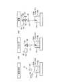
図3に示されるように、検査装置16(装置)は、計測部51と、加工部52と、レーザ干渉計53と、検査部54(異常検出部)と、を有している。計測部51は、造形物101の形状を計測する。加工部52は、造形物101にレーザ光L2を照射することで造形物101の表面101aの一部を除去するとともに、レーザ光L2の照射による衝撃によって造形物101の内部を伝播する弾性波を発生させる。また、加工部52は、計測部51の計測結果に基づいて造形物101の表面101aを加工することにより、造形物101の表面101aの凹凸を減らす、すなわち平坦化することができる。レーザ干渉計53は、弾性波を検出する。検査部54は、弾性波の検出結果に基づいて造形物101を検査する。 As shown in FIG. 3, the inspection device 16 (device) includes a
計測部51は、照明装置55(照明装置)と、カメラ56(撮像部)と、画像処理装置(図示されず)と、を有している。計測部51は、例えば、光切断法で計測対象(層110bや造形物101)の表面の形状を計測する。この場合、照明装置55は、計測対象(層110bや造形物101)の表面に線状の光を照射する。カメラ56は、線状の光を含む画像を撮像する。画像処理装置は、線状の光の位置(基準線とのずれ)に応じて表面の形状の凹凸を測定する。計測部51は、計測した形状(計測結果)を制御部17(図1参照)に送信する。なお、計測部51は、光切断法以外の方式(例えば干渉法等)によって、計測対象の形状を計測してもよい。 The
加工部52は、レーザ出射部60(光源)と、ビームスプリッタ61と、レンズ62(集光レンズ)と、を有している。 The
レーザ出射部60は、発振素子(図示されず)を有し、発振素子の発振によりレーザ光L2を出射する。レーザ光L2は、例えばパルスレーザ光である。レーザ出射部60は、造形物101の固化した材料121を蒸発させることが可能な強度のレーザ光L2を出射する。レーザ出射部60から出射されたレーザ光L2は、ビームスプリッタ61に入射する。 The
ビームスプリッタ61は、レーザ出射部60のレーザ光L2の出射側に位置されている。ビームスプリッタ61は、入射したレーザ光L2の一部を反射する。なお、図3等では、レーザ出射部60から出射されビームスプリッタ61を透過したレーザ光L2の図示は、省略されている。ビームスプリッタ61で反射されたレーザ光L2は、レンズ62に入射する。 The
ビームスプリッタ61からのレーザ光L2は、レンズ62で集光され、造形物101(層110b)の表面101aに照射される。具体的には、レーザ光L2は、例えば複数の層110bの積層方向での造形物101の端面101bに照射される。このとき、レーザ光L2は、造形物101の端面101b(表面101a)の法線方向(層110bの積層方向)に略沿って、当該端面101b(表面101a)に照射される。 The laser beam L2 from the
加工部52は、上述した光学系(第1の光学系)を通じて造形物101に照射したレーザ光L2によって、造形物101の一部の材料を蒸発させることにより、造形物101の一部を除去する。この際、加工部52は、計測部51の計測結果に応じて除去量を変化させることで、表面101a(端面101b)の凹凸を減らす、すなわち端面101b(表面101a)を平坦化することができる。加工部52は、例えば、レーザ光L2の強度を変化させることで、端面101b(表面101a)の除去量を変化させることができる。この場合、表面101aが高いほどレーザ光L2の強度が大きく設定される。加工部52は、端面101bがステージの移動方向(積層方向との直交方向)と平行な平面となるように加工する。 The
また、加工部52は、端面101b(表面101a)へのレーザ光L2の照射の衝撃によって、造形物101の内部に弾性波(密度波)を発生させる。弾性波は、造形物101の内部で、端面101b(表面101a)でのレーザ光L2による加工位置から放射状に伝播する。加工部52は、弾性波発生部および除去部の一例であり、レーザ光L2は、第二のエネルギ線および第一のレーザ光の一例である。 Moreover, the
また、ビームスプリッタ61とレンズ62との間には、光学フィルタ63が設けられている。光学フィルタ63は、ビームスプリッタ61で反射されてレンズ62に向かうレーザ光L2は透過させ、レンズ62から造形物101に照射されて造形物101で反射したレーザ光L2の反射光は透過させないよう、構成されている。また、ビームスプリッタ61のレーザ出射部60とは反対側に、レーザ出射部60から出射されビームスプリッタ61を透過したレーザ光L2を透過させない光学フィルタ(図示されず)を設けることができる。 An
レーザ干渉計53は、レーザ出射部65と、ビームスプリッタ66と、ビームスプリッタ61と、レンズ62と、ミラー67と、検出器64と、を有している。レーザ干渉計53は、造形物101の内部を伝播する弾性波を検出する。レーザ干渉計53は、弾性波検出部の一例である。 The
レーザ出射部65は、発振素子(図示されず)を有し、発振素子の発振によりレーザ光L3を出射する。レーザ光L3は、例えば連続レーザ光(CWレーザ光)またはパルスレーザ光である。レーザ出射部65から出射されたレーザ光L3は、ビームスプリッタ66に入射する。 The
ビームスプリッタ66は、レーザ出射部65のレーザ光L3の出射側に位置されている。ビームスプリッタ66は、入射したレーザ光L3の一部を反射する。ビームスプリッタ61で反射されたレーザ光L3は、レンズ62に入射する。なお、図3等では、レーザ出射部65から出射されビームスプリッタ66を透過したレーザ光L3は、図示されていない。 The
ビームスプリッタ66からのレーザ光L3は、レンズ62で集光され、造形物101(層110b)の端面101b(表面101a)に照射される。このとき、レーザ光L3は、造形物101の端面101b(表面101a)の法線方向に略沿って、当該端面101b(表面101a)に照射される。端面101bに照射されたレーザ光L3は、端面101bで反射され、レンズ62、ビームスプリッタ61、およびビームスプリッタ66を経て、検出光として検出器64に入射する。造形物101の端面101bは、弾性波の造形物101の内部での反射波(弾性波)によって振動する。レーザ干渉計53は、端面101bでの反射光に基づいて、端面101bの変位を検出する。なお、レーザ出射部65は、端面101bで材料121が溶融しない強度のレーザ光L3を出射する。 The laser beam L3 from the
一方、レーザ出射部65から出射されてビームスプリッタ66を経てビームスプリッタ61に入射したレーザ光L3の一部は、ビームスプリッタ61で反射されてミラー67に入射する。 On the other hand, a part of the laser light L 3 emitted from the
ミラー67は、入射したレーザ光L3を反射する。ミラー67で反射されたレーザ光L3の一部は、ビームスプリッタ61およびビームスプリッタ66を経て、参照光として検出器64に入射する。 The
検出器64は、ビームスプリッタ66のビームスプリッタ61とは反対側に位置されている。検出器64は、造形物101の端面101bで反射したレーザ光L3の反射光(検出光)およびミラー67で反射したレーザ光L3の反射光(参照光)を受光する。検出器64は、検出光と参照光との干渉に基づいて端面101bの変位(端面101bの高さの経時変化)を検出することができる。すなわち、検出器64は、造形物101の端面101bでの弾性波(反射波)を検出している。 The
検査部54は、検出器64の検出結果に基づいて、造形物101の内部の異常101cを検出(判定)する。ここで、造形物101の内部に異常101cが無い部分を検査した場合、端面101bで発生した弾性波は、造形物101の底面に到達して底面で反射し、端面101bに戻ってくる。一方、造形物101の内部に異常101cが有る部分を検査した場合、端面101bで発生した弾性波は、異常101cで反射して、端面101bに戻ってくる。すなわち、異常101cが深い位置にあるほど経過時間が長く、異常101cが浅い位置にあるほど経過時間が短い。よって、検査部54は、出射した時点から端面101bの変位が検出された時点までの経過時間または当該経過時間に応じて変化するパラメータに基づいて、異常101cの深さ(位置)を検出することができる。 The
また、異常101cが空洞(ボイド)である場合、当該異常101cが小さく検査した部分の密度が高いほど反射波の強度が小さく、異常101cが大きく検査した部分の密度が低いほど反射波の強度が大きい。よって、検査部54は、反射波の強度(振幅)または当該強度に応じて変化するパラメータに基づいて、異常101cの大きさまたは検査部分の密度を検出することができる。 Further, when the
このように、検査部54は、検出器64の検出結果(弾性波、弾性波信号)に基づいて、造形物101の内部の異常101cの有無、深さ(位置)、密度等を検出することができる。なお、検査部54は、制御部17から得られるレーザ出射部65のレーザ光L3の照射位置を示す情報に基づいて、異常101cの積層方向と直交する平面上での位置を検出することができる。また、検査部54は、例えば、制御部と記憶部とを有する。制御部は、CPU(Central Processing Unit)やコントローラ等を有する。記憶部は、ROM(Read only memory)やRAM(Random Access Memory)等を有する。制御部は、ロードされたプログラム(例えば、OS(Operating System)や、アプリケーション、ウエブアプリケーション等)にしたがって、異常検出に関わる種々の演算処理を実行することができる。 As described above, the
ここで、本実施形態では、図3に示されるように、一つのレンズ62が、レーザ光L2を集光するとともにレーザ光L3を集光している。ただし、図4に示されるように、レンズ62によるレーザ光L2の集光位置(集束位置)と、レンズ62によるレーザ光L3の集光位置(集束位置)とは、互いに異なっている。具体的には、造形物101を基準とするレーザ光L2,L3、すなわち検査装置16の相対的な移動方向(図3中の矢印A方向)において、レーザ光L3の照射位置P3は、レーザ光L2の照射位置P2よりも後方(上流側)に位置している。これにより、端面101bの、レーザ光L2によって凹凸が減らされたすなわち平坦化された位置にレーザ光L3が照射され、当該位置での反射波(弾性波)による変位が検出される。よって、本実施形態によれば、例えば、レーザ光L2によって凹凸が減らされていない位置にレーザ光L3が照射され、当該位置での反射波(弾性波)による変位が検出される場合に比べて、変位がより精度よく検出されうる。なお、図3中の矢印Bは、移動装置13の駆動によって移動するステージ12(造形物101)の移動方向を示している。 Here, in the present embodiment, as shown in FIG. 3, one
また、本実施形態では、レーザ光L2(第一のレーザ光)とレーザ光L3(第二のレーザ光)とが互いに干渉しないように、それらの波長が互いに異なってもよい。具体的には、例えば、レーザ光L2の波長が、レーザ光L3の波長より短くてもよい。また、レーザ光L2とレーザ光L3とが互いに干渉しないように、それらの偏光方向(偏光面)が互いに異なってもよい。具体的には、例えば、レーザ光L2およびレーザ光L3のうち一方がP偏光で、他方がS偏光であってもよい。 In the present embodiment, the wavelengths of the laser beam L2 (first laser beam) and the laser beam L3 (second laser beam) may be different from each other so as not to interfere with each other. Specifically, for example, the wavelength of the laser beam L2 may be shorter than the wavelength of the laser beam L3. Further, their polarization directions (polarization planes) may be different from each other so that the laser beam L2 and the laser beam L3 do not interfere with each other. Specifically, for example, one of the laser light L2 and the laser light L3 may be P-polarized light and the other may be S-polarized light.
また、レーザ光L2のパルス幅が小さいほど、弾性波が高周波になり分解能が上がるため、より小さい異常101cを検出しやすくなるが、レーザ光L2のパルス幅が小さいほど、すなわち弾性波の周波数が高いほど、弾性波が造形物101に吸収され弾性波の検出が困難になりやすい。したがって、レーザ光L2のパルス幅は、検出する異常101cの大きさに応じて設定される。例えば、大きさが数μm以上の異常101cに対して、レーザ光L2のパルス幅が1fs以上1ns以下に設定されうる。 In addition, the smaller the pulse width of the laser beam L2, the higher the elastic wave becomes and the higher the resolution. Therefore, it becomes easier to detect the
制御部17は、一例として、CPU(Central Processing Unit)と記憶部とを有する。記憶部は、ROM(Read Only Memory)やRAM(Random Access Memory)等を有する。制御部17は、移動装置13、光学装置15、搬送装置24、供給装置31、および検査装置16に、信号線220を介して電気的に接続されている。制御部17(CPU)は、ロードされたプログラム(例えば、OS(Operating System)や、アプリケーション、ウエブアプリケーション等)にしたがって、移動装置13、光学装置15、搬送装置24、供給装置31、および検査装置16を制御する。積層造形装置1は、制御部17の制御(プログラム)に基づき、積層造形物100を造形する。 For example, the
制御部17は、移動装置13を制御することで、ステージ12を三軸方向に移動させる。制御部17は、搬送装置24を制御することで、造形した積層造形物100を副室22に搬送する。制御部17は、供給装置31を制御することで、材料121の供給の有無ならびに供給量を調整する。制御部17は、レーザ出射部41を制御することで、レーザ出射部41,60,65から出射されるレーザ光L1,L2,L3の強度(パワー密度)を調整する。また、制御部17は、移動装置(図示されず)を制御することで、ノズル33の移動を制御する。また、制御部17は、移動装置(図示されず)を制御することで、検査装置16の移動を制御する。 The
制御部17の記憶部は、造形する積層造形物100の形状(参照形状)を示すデータ等を記憶している。この形状データは、各層110bの形状(参照形状)のデータを含む。 The storage unit of the
制御部17は、層110bまたは積層造形物100の形状を判断する機能を備えている。制御部17は、計測部51が計測した層110bまたは積層造形物100の形状と、記憶部に記憶された参照形状と比較することで、所定の形状でない部位が形成されているか否かを判断する。 The
また、制御部17は、層110bまたは積層造形物100の形状を所定の形状にトリミングする機能を備えている。制御部17は、層110bまたは積層造形物100における所定の形状でない部位(除去する部位)を蒸発させることが可能なレーザ光L2の強度となるように、加工部52のレーザ出射部60を制御する。次いで、制御部17は、レーザ光L2が当該部位に照射されるように、加工部52および移動装置13を制御する。これにより、当該部位が蒸発する。 In addition, the
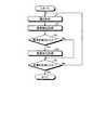
次に、積層造形装置1が積層造形物100を造形する手順(積層造形物100の製造方法)の一例について、図5のフローチャートを参照して説明する。 Next, an example of a procedure for manufacturing the layered object 100 (method for manufacturing the layered object 100) by the
まず、制御部17は、層110bが形成されるよう、移動装置13、ノズル装置14、および光学装置15を制御する(S1)。S1では、記憶部に記憶された層110bのデータ(参照データ)に基づいて、材料121が供給されレーザ光L1が照射される。このとき、制御部17は、材料121がノズル33から所定の範囲に供給されるよう移動装置13および供給装置31等を制御するとともに、供給された材料121がレーザ光L1によって溶融するよう、レーザ出射部41を制御する。これにより、ベース110a上の層110bを形成する範囲に、溶融した材料121が所定量供給される。このとき、本実施形態では、形成される層110bの高さが記憶部に記憶された層110bのデータの高さよりも高くなるように材料121が供給される。材料121は、ベース110aや層110bに噴射あるいは押し出されると、層状または薄膜状等の材料121の集合となる。このとき、材料121は、材料121を運ぶキャリアガスによって冷却されるか若しくは材料121の集合への伝熱によって冷却されることで固化されて、層110bを構成する。この際、制御部17は、アニール処理を行ってよい。アニール処理では、制御部17は、ベース110a上の層110bにレーザ光L1が照射されるよう、レーザ出射部41を制御する。これにより、層110bの材料121が再溶融された後、再び固化する。なお、アニール処理は、積層造形装置1の外でアニール装置(図示されず)を用いて行ってもよい。 First, the
次に、制御部17は、造形物101の内部が検査されるよう、検査装置16および移動装置13を制御する(S2:異常検出処理(検査処理))。図6に示されるように、S2では、形状測定、トリミング、および検査が実行される。まず、制御部17は、造形物101の層110bの表面101aの形状(表面形状、三次元形状)が計測されるよう計測部51および移動装置13を制御する。制御部17は、当該層110bの形状を示す計測形状データを計測部51から取得する。次に、制御部17は、造形物101の端面101b(表面101a)がトリミングされるよう、加工部52および移動装置13を制御する。この際、制御部17は、層110bの高さが記憶部に記憶された層110bのデータの高さ(一例として、一定の高さ)と略同じとなるように、加工部52および移動装置13を制御する。このとき、制御部17は、層110bの端面101bの高さ(層110bの厚さ)が略一定となるように、計測した層110bの端面101bの高さ(凹凸)に応じて端面101bの除去量を変化させる。具体的に、制御部17は、除去量に応じたレーザ光L2の強度となるように、加工部52を制御する。これにより、例えば、次の層110bがより平坦に形成されやすくなったり、弾性波の検査の精度がより高まりやすくなったりといった効果が得られる。トリミングは、加工部52によるレーザ光L2の照射によってなされる。そして、レーザ干渉計53が、レーザ光L2の照射によって発生した弾性波をレーザ光L3を用いて検出し、検査部54が、レーザ干渉計53の検出結果に基づいて造形物101の内部の異常101cの有無を検出(判定)する。異常101cの有無の検出は、レーザ光L2が出射される毎に行われる。本実施形態では、端面101bの全域に対して、異常101cの有無の検出が行われる。また、制御部17は、上記トリミングの際に、記憶部に記憶された層110bの参照形状データと、計測部51の計測結果である計測形状データとの比較により、本来造形されるべきではない部分(領域)に造形がされていた場合、当該部分を除去する。例えば、制御部17は、積層方向との直交方向で本来造形されるべきではない部分(領域)に造形がされていた場合、当該部分を除去する。 Next, the
S2は、一つの層110bが形成される毎に実行されてもよいし複数の層110bが形成される毎に実行されてもよい。S2は、層110bが形成された後に実行される。なお、形状測定およびトリミングは一つの層110bが形成される毎に行われ、弾性波検出は複数の層110bが形成される毎に行われてもよい。 S2 may be executed every time one
そして、図5に示されるように、検査装置16(の検査部54)が造形物101の内部の異常101cを検出した場合(S3でYes)、制御部17は、異常101cを修復する(除去する)(S4:修復加工処理)。異常101cが空洞(ボイド)である場合、図7に示されるように、S4では、開口部形成、造形(穴埋め)、および突出部分の除去が実行される。まず、制御部17は、造形物101のうち端面101b(表面101a)と異常101cとの間の部分、すなわち、造形物101のうち異常101cより端面101b側の部分が除去されるよう、加工部52および移動装置13を制御する。これにより、造形物101には、異常101cを底部とする開口部101dが形成される。次に、制御部17は、開口部101dが材料121で埋められるとともに当該材料121を固化させるよう、造形部18を制御する。このとき、造形部18は、例えば、材料121が開口部101dから突出するまで造形を行う。次に、制御部17は、開口部101dから突出した造形物101の少なくとも一部、すなわち開口部101dから突出した造形物101の部分の全部または一部が除去されるよう、加工部52を制御する。詳細には、制御部17は、開口部101dから突出した突出部分(材料121)が蒸発するよう、加工部52のレーザ出射部60を制御する。このように突出部分が除去されることで、穴埋めされた部分がより平坦化されやすい。なお、S4は、複数の層110bが形成される毎に行われてもよい。 Then, as illustrated in FIG. 5, when the inspection device 16 (the inspection unit 54) detects the
一方、検査装置16が造形物101の内部の異常101cを検出しなかった場合(S3のNo)、S4は実行されない。 On the other hand, when the
次に、図5に示されるように、全ての層110bが形成されていない場合(S5でNo)、S1に戻って、既に形成された層110bの上に新たな層110bが形成される。制御部17は、S1〜S5の処理を繰り返し行って複数の層110bを積み重ねる。そして、全ての層110bが形成されると(S5でYes)、一連の処理が終了する。 Next, as shown in FIG. 5, when all the
以上説明したように、本実施形態では、造形部18が、粉末状(あるいは線状)の材料121にレーザ光L1(第一のエネルギ線)を照射し材料121を固化させて形成する層110bを、順次積層し、加工部52(弾性波発生部)が、一つ以上の層110bによって構成された造形物101の内部を伝播する弾性波を発生させ、レーザ干渉計53が、弾性波を検出し、検査部54が、レーザ干渉計53の検出結果に基づいて、造形物101を検査する。よって、造形物101の内部の異常101cを検出することができる。 As described above, in the present embodiment, the
また、本実施形態では、加工部52は、レーザ光L2(第二のエネルギ線)の照射によって造形物101の表面101aを加工する。加工部52は、表面101aにレーザ光l2を照射することによって弾性波を発生させる。つまり、加工部52が、弾性波発生部として機能するので、弾性波発生部を加工部52とは別に設ける構成に比べて、積層造形装置1の構成が簡素化されやすい。 Moreover, in this embodiment, the
また、本実施形態では、レーザ光L2(第一のレーザ光)とレーザ光L3(第二のレーザ光)とは、互いに干渉しない。よって、造形物101の内部の異常101cの高い検出精度が得やすい。 In the present embodiment, the laser beam L2 (first laser beam) and the laser beam L3 (second laser beam) do not interfere with each other. Therefore, it is easy to obtain high detection accuracy of the
また、本実施形態では、一つのレンズ62が、レーザ光L2の集光とレーザ光L3の集光とを行う。よって、レーザ光L2の集光とレーザ光L3の集光とを別々のレンズによって行う構成に比べて、積層造形装置1の構成が簡素化されやすい。 In the present embodiment, one
また、本実施形態では、加工部52(除去部)は、造形物101の一部を除去可能である。そして、検査部54が造形物101の内部の異常101cを検出した場合、加工部52が、造形物101の表面101aから異常101cまでの造形物101の一部を除去し、造形部18が、加工部52の除去によって形成された造形物101の開口部101dを材料121で埋めて且つ当該材料121を固化させる。よって、異常101cが除去され修復された造形物101が得られる。 Moreover, in this embodiment, the process part 52 (removal part) can remove some modeling objects 101. FIG. And when the
(第2の実施形態)
本実施形態の積層造形装置1Aは、第1の実施形態の積層造形装置1と同様の構成を備えている。ただし、本実施形態では、図8に示されるように、検査装置16Aが第1の実施形態の検査装置16と異なる。(Second Embodiment)
The additive manufacturing apparatus 1A of the present embodiment has the same configuration as the
検査装置16Aは、計測部51と、加工部52Aと、レーザ干渉計53Aと、検査部54と、を有している。 The
本実施形態では、加工部52Aやレーザ干渉計53Aを構成する部材として、レーザ出射部201(光源)と、ビームスプリッタ61,66,202と、ミラー67,203と、レンズ62(集光レンズ)と、波長変換素子204と、光量調整部材205と、検出器64と、が設けられている。加工部52Aは、レーザ出射部201と、ビームスプリッタ61,202と、ミラー203と、レンズ62と、を有している。一方、レーザ干渉計53Aは、レーザ出射部201と、ビームスプリッタ61,66,202と、レンズ62と、ミラー67と、波長変換素子204と、光量調整部材205と、検出器64と、を有している。加工部52Aは、弾性波発生部および除去部の一例である。 In the present embodiment, as members constituting the
レーザ出射部201は、発振素子(図示されず)を有し、発振素子の発振によりレーザ光L4を出射する。レーザ光L4は、例えばパルスレーザ光である。レーザ光L4は、第三のレーザ光の一例である。 The
レーザ出射部201から出射されたレーザ光L2は、ビームスプリッタ202に入射して、ビームスプリッタ202によって、レーザ光L2とレーザ光L3とに分離される。ビームスプリッタ202は、分離部の一例である。 The laser beam L2 emitted from the
レーザ光L2は、ミラー203で反射されて、ビームスプリッタ61に入射する。レーザ光L2の一部は、ビームスプリッタ61で反射され、レンズ62によって集光され、造形物101の端面101bに照射される。 The laser beam L2 is reflected by the
一方、レーザ光L3は、波長変換素子204および光量調整部材205に順に入射し、波長変換素子204によって波長が変換され、光量調整部材205によって光量が減少される。光量調整部材205から出射されたレーザ光L3は、ビームスプリッタ66に入射する。レーザ光L3の一部は、ビームスプリッタ66によって反射されて、ビームスプリッタ61に入射する。ビームスプリッタ61に入射されたレーザ光L3は、第1の実施形態と同様に、レンズ62に入射する光と、ミラー67に入射する光とに分離される。レンズ62に入射されたレーザ光L3は、レンズ62によって集光され、造形物101の端面101bに照射される。造形物101の端面101bに照射されたレーザ光L3は、端面101bで反射されて、レンズ62、ビームスプリッタ61、およびビームスプリッタ66を経て、検出器64に入射する。一方、ミラー67で反射されたレーザ光L3は、ビームスプリッタ61およびビームスプリッタ66を経て、検出器64に入射する。なお、レーザ光L3は、端面101bで材料121が溶融しない強度となるように、光量調整部材205によって光量が減少される。 On the other hand, the laser beam L3 sequentially enters the
また、本実施形態でも、第1の実施形態と同様に、一つのレンズ62が、レーザ光L2を集光するとともにレーザ光L3を集光している。また、レンズ62によるレーザ光L2の集光位置(集束位置)と、レンズ62によるレーザ光L3の集光位置(集束位置)とは、互いに異なっている。具体的には、造形物101を基準とするレーザ光L2,L3、すなわち検査装置16Aの相対的な移動方向(矢印A方向)において、レーザ光L3の照射位置P3は、レーザ光L2の照射位置P2よりも後方(上流側)に位置している。 Also in this embodiment, similarly to the first embodiment, one
また、本実施形態では、波長変換素子204によってレーザ光L2のレーザ光L3の波長が変換されることにより、レーザ光L3とレーザ光L2とが重なった場合でも互いに干渉しなくなる。 In the present embodiment, the wavelength of the laser beam L3 of the laser beam L2 is converted by the
以上説明したように、本実施形態では、一つのレーザ出射部201が、レーザ光L4(第三のレーザ光)を出射し、ビームスプリッタ202(分離部)が、レーザ出射部201から出射されたレーザ光L4を、レーザ光L2(第一のレーザ光)とレーザ光L3(第二のレーザ光)とに分離させる。よって、レーザ出射部201のレーザ光L2,L3のそれぞれに対してレーザ出射部が設けられた構成に比べて、レーザ出射部201の数を減らすことができる。 As described above, in this embodiment, one
なお、上記各実施形態では、例えば、供給装置31が種類の異なる複数の材料121をノズル33に供給して、ノズル33から複数の異なる材料121を選択的に供給し、複数の材料121の比率を調整(変更)するようにしてもよい。これにより、積層造形物100の位置(場所)によって複数の材料121の比率が変化(漸減または漸増)する傾斜材料(傾斜機能材料)を造形することができる。具体的には、例えば、層110bの形成に際し、制御部17が、積層造形物100の三次元座標の各位置に対応して設定された(記憶された)材料121の比率となるように、供給装置31を制御することにより、積層造形物100を、材料121の比率が三次元の任意の方向に変化する傾斜材料(傾斜機能材料)として造形することが可能である。単位長さあたりの材料121の比率の変化量(変化率)も、種々に設定することが可能である。 In each of the above embodiments, for example, the
以上説明したとおり、上記各実施形態によれば、例えば、造形物101の内部の異常101cを検出することができる積層造形装置1,1Aおよび積層造形方法を得ることができる。 As described above, according to each of the above embodiments, for example, the
本発明のいくつかの実施形態を説明したが、これらの実施形態は、例として提示したものであり、発明の範囲を限定することは意図していない。これら新規な実施形態は、その他の様々な形態で実施されることが可能であり、発明の要旨を逸脱しない範囲で、種々の省略、置き換え、変更を行うことができる。これら実施形態やその変形は、発明の範囲や要旨に含まれるとともに、特許請求の範囲に記載された発明とその均等の範囲に含まれる。 Although several embodiments of the present invention have been described, these embodiments are presented by way of example and are not intended to limit the scope of the invention. These novel embodiments can be implemented in various other forms, and various omissions, replacements, and changes can be made without departing from the scope of the invention. These embodiments and modifications thereof are included in the scope and gist of the invention, and are included in the invention described in the claims and the equivalents thereof.
例えば、積層造形装置は、材料供給部によって粉末状の材料を供給して材料層を形成する工程と、該材料層に照射装置によってレーザ光等の第一のエネルギ線を照射することにより、材料を固化させる工程と、を繰り返し行うことにより、個化層(層)を積層させて造形を行う構成(パウダーベッド方式)等であってもよい。この場合も、開口部101dから突出した材料121の除去は、必要に応じて行うようにしてよい。例えば、材料層の高さよりも、開口部101dから突出した材料121の高さが低い場合には、当該材料121を除去しなくてもよい。 For example, the additive manufacturing apparatus supplies a powder material by a material supply unit to form a material layer, and irradiates the material layer with a first energy beam such as a laser beam by using an irradiation device. The structure (powder bed system) etc. which laminate | stack an individualization layer (layer) and shape | mold by repeating the process to solidify may be sufficient. Also in this case, the
また、上記各実施形態では、加工部52から出射したレーザ光L2によるアブレーションモードによって弾性波を発生させたが、加工部52とは別にレーザ光を出射する構成を設け、当該レーザ光による熱応力モードによって弾性波を発生させてもよい。 In each of the above embodiments, the elastic wave is generated by the ablation mode by the laser beam L2 emitted from the
1,1A…積層造形装置、18…造形部、51…計測部、52,52A…加工部(弾性波発生部、除去部)、53,53A…レーザ干渉計(弾性波検出部)、54…検査部、62…レンズ、101…造形物、101a…表面、101c…異常、101d…開口部、110b…層、201…レーザ出射部、202…ビームスプリッタ(分離部)、L1…レーザ光(第一のエネルギ線)、L2…レーザ光(第二のエネルギ線、第一のレーザ光)、L3…レーザ光(第二のレーザ光)、L4…レーザ光(第三のレーザ光)。 DESCRIPTION OF
Claims (15)
Translated fromJapanese第二のエネルギ線の照射によって、前記層によって構成された造形物の表面を加工するとともに前記造形物の内部を伝播する弾性波を発生させる加工部と、
前記弾性波を検出する弾性波検出部と、
前記弾性波検出部の検出結果に基づいて、前記造形物を検査する検査部と、
を備えた積層造形装置。A layer formed by sequentially laminating the material by irradiating the material with the first energy ray and solidifying the material; and
Aprocessing unit that generates an elastic wave that propagates throughthe inside of themodeled object while processing thesurface of the modeled object constituted by the layer byirradiation with the second energy ray ;
An elastic wave detector for detecting the elastic wave;
Based on the detection result of the elastic wave detection unit, an inspection unit for inspecting the modeled object,
An additive manufacturing apparatus comprising:
前記加工部は、前記計測部の計測結果に基づいて前記表面を加工する、請求項1に記載の積層造形装置。A measuring unit for measuring the shape of the layer;
The additive manufacturing apparatus according to claim1 , wherein the processing unit processes the surface based on a measurement result of the measurement unit.
前記弾性波検出部は、前記表面に第二のレーザ光を照射し、前記表面で反射した前記第二のレーザ光の反射光を受光するレーザ干渉計であり、
前記第一のレーザ光と前記第二のレーザ光とは、互いに干渉しない、請求項1〜3のいずれか一項に記載の積層造形装置。The second energy ray is a first laser beam,
The elastic wave detection unit is a laser interferometer that irradiates the surface with a second laser beam and receives the reflected light of the second laser beam reflected on the surface,
The additive manufacturing apparatus according to any one of claims1 to3 , wherein the first laser light and the second laser light do not interfere with each other.
前記レーザ出射部から出射された前記第三のレーザ光を、前記第一のレーザ光と前記第二のレーザ光とに分離させる分離部と、
を備えた請求項4または5に記載の積層造形装置。One laser emitting section for emitting a third laser beam;
A separation unit that separates the third laser light emitted from the laser emission unit into the first laser light and the second laser light;
Layered manufacturing device according to claim4 or5 with a.
前記検査部が前記造形物の内部の異常を検出した場合、前記除去部が、前記造形物の表面から前記異常までの前記造形物の一部を除去し、前記造形部が、前記除去部の除去によって形成された前記造形物の開口部を前記材料で埋めて且つ当該材料を固化させる、請求項1〜6のいずれか一項に記載の積層造形装置。A removal unit capable of removing a part of the modeled object,
When the inspection unit detects an abnormality inside the modeled object, the removing unit removes a part of the modeled object from the surface of the modeled object to the abnormality, and the modeled unit is connected to the removed unit. The additive manufacturing apparatus according to any one of claims 1 to6 , wherein an opening of the modeled object formed by removal is filled with the material and the material is solidified.
前記表面に第二のレーザ光を照射する工程と、前記表面で反射した前記第二のレーザ光の反射光を受光して前記弾性波を検出する工程とを有し、
前記第一のレーザ光と前記第二のレーザ光とは、互いに干渉しない、請求項9〜11のいずれか一項に記載の積層造形方法。The second energy ray is a first laser beam,
Irradiating the surface with a second laser beam, and receiving the reflected light of the second laser beam reflected on the surface to detect the elastic wave,
The additive manufacturing method according to any one of claims9 to11 , wherein the first laser beam and the second laser beam do not interfere with each other.
Priority Applications (6)
| Application Number | Priority Date | Filing Date | Title |
|---|---|---|---|
| JP2014187982AJP5905060B1 (en) | 2014-09-16 | 2014-09-16 | Additive manufacturing apparatus and additive manufacturing method |
| CN201580047373.7ACN106604810B (en) | 2014-09-16 | 2015-02-23 | Lamination manufacturing device and lamination manufacturing method |
| DE112015004212.1TDE112015004212T5 (en) | 2014-09-16 | 2015-02-23 | Additive manufacturing device and additive manufacturing process |
| PCT/JP2015/055080WO2016042794A1 (en) | 2014-09-16 | 2015-02-23 | Laminate shaping apparatus and laminate shaping method |
| US15/505,448US20170266727A1 (en) | 2014-09-16 | 2015-02-23 | Additive manufacturing apparatus and additive manufacturing method |
| US16/801,324US11318536B2 (en) | 2014-09-16 | 2020-02-26 | Additive manufacturing apparatus and additive manufacturing method |
Applications Claiming Priority (1)
| Application Number | Priority Date | Filing Date | Title |
|---|---|---|---|
| JP2014187982AJP5905060B1 (en) | 2014-09-16 | 2014-09-16 | Additive manufacturing apparatus and additive manufacturing method |
Publications (2)
| Publication Number | Publication Date |
|---|---|
| JP5905060B1true JP5905060B1 (en) | 2016-04-20 |
| JP2016060063A JP2016060063A (en) | 2016-04-25 |
Family
ID=55532845
Family Applications (1)
| Application Number | Title | Priority Date | Filing Date |
|---|---|---|---|
| JP2014187982AExpired - Fee RelatedJP5905060B1 (en) | 2014-09-16 | 2014-09-16 | Additive manufacturing apparatus and additive manufacturing method |
Country Status (5)
| Country | Link |
|---|---|
| US (2) | US20170266727A1 (en) |
| JP (1) | JP5905060B1 (en) |
| CN (1) | CN106604810B (en) |
| DE (1) | DE112015004212T5 (en) |
| WO (1) | WO2016042794A1 (en) |
Cited By (2)
| Publication number | Priority date | Publication date | Assignee | Title |
|---|---|---|---|---|
| JPWO2020090074A1 (en)* | 2018-10-31 | 2021-09-24 | 株式会社ニコン | Processing system and processing method |
| JP2024086918A (en)* | 2019-04-09 | 2024-06-28 | 株式会社ニコン | Modeling Unit |
Families Citing this family (44)
| Publication number | Priority date | Publication date | Assignee | Title |
|---|---|---|---|---|
| US10065367B2 (en)* | 2015-03-20 | 2018-09-04 | Chevron Phillips Chemical Company Lp | Phonon generation in bulk material for manufacturing |
| EP3159081B1 (en)* | 2015-10-21 | 2023-12-06 | Nikon SLM Solutions AG | Powder application arrangement comprising two cameras |
| US11073501B2 (en)* | 2015-11-13 | 2021-07-27 | Honeywell Federal Manufacturing & Technologies, Llc | System and method for inspecting parts using dynamic response function |
| US10073060B2 (en)* | 2015-11-19 | 2018-09-11 | General Electric Company | Non-contact acoustic inspection method for additive manufacturing processes |
| WO2017181151A1 (en) | 2016-04-14 | 2017-10-19 | Cornell University | Methods for incremental 3d printing and 3d printing arbitrary wireframe meshes |
| CN105834426B (en)* | 2016-05-24 | 2018-12-21 | 苏州大学 | Cavity part laser 3D forming technology |
| US20170355018A1 (en)* | 2016-06-09 | 2017-12-14 | Hamilton Sundstrand Corporation | Powder deposition for additive manufacturing |
| JP6817561B2 (en)* | 2016-06-30 | 2021-01-20 | パナソニックIpマネジメント株式会社 | Manufacturing method of 3D shaped object |
| US11513080B2 (en)* | 2016-09-09 | 2022-11-29 | Hamilton Sundstrand Corporation | Inspection systems for additive manufacturing systems |
| DE102016124695A1 (en)* | 2016-12-16 | 2018-06-21 | Cl Schutzrechtsverwaltungs Gmbh | Exposure device for a device for the additive production of three-dimensional objects |
| JP6961968B2 (en)* | 2017-03-22 | 2021-11-05 | 日本電気株式会社 | Laminated modeling inspection device, laminated modeling device and laminated modeling method |
| WO2018178387A1 (en) | 2017-03-31 | 2018-10-04 | Precitec Gmbh & Co. Kg | Device and method for an additive manufacture |
| JP6877312B2 (en)* | 2017-10-16 | 2021-05-26 | 株式会社東芝 | Additional manufacturing method and additional manufacturing system |
| EP3495143B1 (en)* | 2017-12-08 | 2021-07-07 | CL Schutzrechtsverwaltungs GmbH | Apparatus and method for additively manufacturing three-dimensional objects |
| EP3711929A4 (en)* | 2017-12-20 | 2021-07-28 | Mitsui Chemicals, Inc. | STEREOLITHOGRAPHY DEVICE, STEREOLITHOGRAPHY PROGRAM AND STEREOLITHOGRAPHY METHOD |
| DE102018101522A1 (en)* | 2018-01-24 | 2019-07-25 | Lunovu Gmbh | Method and apparatus for applying a three-dimensional structure to a surface of a workpiece |
| EP3536485B1 (en)* | 2018-03-09 | 2024-06-12 | Concept Laser GmbH | Apparatus for additively manufacturing three-dimensional objects |
| JP6749361B2 (en)* | 2018-03-30 | 2020-09-02 | 株式会社フジクラ | Irradiation apparatus, metal modeling apparatus, metal modeling system, irradiation method, and metal modeling object manufacturing method |
| JP7056411B2 (en)* | 2018-06-29 | 2022-04-19 | 株式会社リコー | Reading device and modeling device |
| FR3083158B1 (en)* | 2018-06-29 | 2020-06-19 | Safran | DEVICE AND METHOD FOR DIRECT MANUFACTURE BY LASER SPRAYING OF POWDERED POWDER |
| JP7030635B2 (en)* | 2018-07-06 | 2022-03-07 | 株式会社東芝 | Addition manufacturing method and addition manufacturing system |
| CN109746443A (en)* | 2018-12-29 | 2019-05-14 | 华中科技大学 | A Method for Parallel Control of Part Deformation and Accuracy During Additive Manufacturing |
| WO2020169455A1 (en)* | 2019-02-19 | 2020-08-27 | Siemens Aktiengesellschaft | Additive manufacture of a workpiece |
| JP2020153718A (en)* | 2019-03-18 | 2020-09-24 | 株式会社リコー | Measuring equipment and modeling equipment |
| CN110196231B (en)* | 2019-05-14 | 2021-09-07 | 东南大学 | A laser ultrasonic offline detection device and method for additive parts |
| FR3096297B1 (en)* | 2019-05-23 | 2024-01-19 | Inst De Rech Tech Jules Verne | Process for repairing a part during additive manufacturing |
| CA3145642A1 (en)* | 2019-07-03 | 2021-01-07 | Norsk Titanium As | Standoff distance monitoring and control for directed energy deposition additive manufacturing systems |
| JP6915006B2 (en)* | 2019-08-29 | 2021-08-04 | 株式会社ソディック | Metal powder additive manufacturing method and metal powder additive manufacturing equipment |
| DE112020004392T5 (en) | 2019-09-20 | 2022-06-02 | Shibaura Machine Co., Ltd. | Additive manufacturing system |
| DE102019007972B4 (en)* | 2019-11-17 | 2025-07-10 | 3D Systems Gmbh | Apparatus and method for producing a three-dimensional shaped article |
| KR102236148B1 (en)* | 2019-12-31 | 2021-04-06 | 한국과학기술원 | 3D printing system and method for controlling the size of molten pool formed during 3D printing process |
| KR102226094B1 (en)* | 2019-12-31 | 2021-03-11 | 한국과학기술원 | Method and apparatus for inspecting layering quality of printing objects using femeto-second laser beam in 3d printing process and 3d printing system having the same |
| KR102194695B1 (en)* | 2019-12-31 | 2020-12-24 | 한국과학기술원 | Method and apparatus for estimating the height of a laminated portion formed in a 3D printing process, and 3D printing system having the same |
| KR102220823B1 (en) | 2019-12-31 | 2021-02-26 | 한국과학기술원 | Method and apparatus for estimating depth of molecular pull during 3d processing, and 3d printing system having the same |
| KR102235761B1 (en)* | 2019-12-31 | 2021-04-02 | 한국과학기술원 | Apparatus for measuring ultrasonic based on femtosecond laser in 3D printing process and 3D printing system having the same |
| JP7481132B2 (en)* | 2020-03-13 | 2024-05-10 | 三菱重工業株式会社 | DEFECT DETECTION METHOD, DEFECT DETECTION APPARATUS, AND FORMING APPARATUS |
| JP7103379B2 (en)* | 2020-03-23 | 2022-07-20 | 株式会社ニコン | Three-dimensional model manufacturing equipment |
| US11680909B2 (en)* | 2020-05-14 | 2023-06-20 | The Boeing Company | Automated inspection of foreign materials, cracks and other surface anomalies |
| DE102020127581A1 (en)* | 2020-10-20 | 2022-04-21 | Carl Zeiss Ag | Method and device for the additive manufacturing of a workpiece |
| WO2022176430A1 (en)* | 2021-02-18 | 2022-08-25 | 国立大学法人大阪大学 | Method for manufacturing three-dimensional structure, and fabrication device |
| JP7609702B2 (en)* | 2021-05-11 | 2025-01-07 | 三菱重工業株式会社 | Defect Detection Method |
| JP7609709B2 (en)* | 2021-05-31 | 2025-01-07 | 三菱重工業株式会社 | Defect detection device and defect detection method |
| KR102512669B1 (en)* | 2021-08-13 | 2023-03-22 | 한국생산기술연구원 | 3d printing apparatus using a voxel-by-boxel multi-materials |
| US12196543B2 (en)* | 2022-04-06 | 2025-01-14 | The Boeing Company | System for in-process inspection of fused-filament fabricated parts and associated methods |
Family Cites Families (23)
| Publication number | Priority date | Publication date | Assignee | Title |
|---|---|---|---|---|
| JPS59162451A (en)* | 1983-03-07 | 1984-09-13 | Hitachi Ltd | Device for detecting defect in painted film |
| JP2502184B2 (en) | 1990-10-09 | 1996-05-29 | 動力炉・核燃料開発事業団 | Laser ultrasonic flaw detection method and device |
| JPH04366761A (en) | 1991-06-13 | 1992-12-18 | Hitachi Ltd | Ultrasonic testing method |
| JPH0596632A (en)* | 1991-10-08 | 1993-04-20 | Daikin Ind Ltd | Optical modeling method and apparatus |
| SE521124C2 (en)* | 2000-04-27 | 2003-09-30 | Arcam Ab | Device and method for making a three-dimensional product |
| JP3801100B2 (en)* | 2002-06-07 | 2006-07-26 | Jsr株式会社 | Photo-curing modeling apparatus, photo-curing modeling method, and photo-curing modeling system |
| JP3673782B2 (en)* | 2002-09-25 | 2005-07-20 | キヤノン株式会社 | Liquid ejection head, liquid ejection head driving method, and liquid ejection apparatus |
| US6955416B2 (en) | 2002-06-14 | 2005-10-18 | Canon Kabushiki Kaisha | Ink-jet head, its driving method, and ink-jet recording apparatus |
| AU2003900180A0 (en)* | 2003-01-16 | 2003-01-30 | Silverbrook Research Pty Ltd | Method and apparatus (dam001) |
| JP3599059B2 (en)* | 2003-02-25 | 2004-12-08 | 松下電工株式会社 | Method and apparatus for manufacturing three-dimensional shaped object |
| DE112004000302B3 (en) | 2003-02-25 | 2010-08-26 | Panasonic Electric Works Co., Ltd., Kadoma-shi | Method and device for producing a three-dimensional object |
| US7397596B2 (en)* | 2004-07-28 | 2008-07-08 | Ler Technologies, Inc. | Surface and subsurface detection sensor |
| JP4519560B2 (en)* | 2004-07-30 | 2010-08-04 | 株式会社メディアプラス | Additive manufacturing method |
| JP2006200030A (en) | 2005-01-24 | 2006-08-03 | Aisan Ind Co Ltd | Method and device for producing cubic molding |
| GB0601982D0 (en)* | 2006-02-01 | 2006-03-15 | Rolls Royce Plc | Method and apparatus for examination of objects and structures |
| US7729881B2 (en)* | 2007-01-08 | 2010-06-01 | Bossa Nova Technologies, Llc | Laser intensity noise rejection for interferometric apparatus |
| JP2008254241A (en)* | 2007-04-02 | 2008-10-23 | Hitachi Kokusai Electric Inc | Stereolithography equipment |
| JP2009274338A (en)* | 2008-05-15 | 2009-11-26 | Hitachi Kokusai Electric Inc | Device for laser beam lithography |
| US8822875B2 (en) | 2010-09-25 | 2014-09-02 | Queen's University At Kingston | Methods and systems for coherent imaging and feedback control for modification of materials |
| JP2012163406A (en)* | 2011-02-04 | 2012-08-30 | Toshiba Corp | Material inspection/repair device and material inspection/repair method |
| JP5861117B2 (en)* | 2011-05-30 | 2016-02-16 | パナソニックIpマネジメント株式会社 | Manufacturing method and manufacturing apparatus for three-dimensional shaped object |
| US20150201500A1 (en)* | 2014-01-12 | 2015-07-16 | Zohar SHINAR | System, device, and method of three-dimensional printing |
| WO2015109096A1 (en)* | 2014-01-17 | 2015-07-23 | United Technologies Corporation | An additive manufacturing system with ultrasonic inspection and method of operation |
- 2014
- 2014-09-16JPJP2014187982Apatent/JP5905060B1/ennot_activeExpired - Fee Related
- 2015
- 2015-02-23DEDE112015004212.1Tpatent/DE112015004212T5/enactivePending
- 2015-02-23CNCN201580047373.7Apatent/CN106604810B/enactiveActive
- 2015-02-23WOPCT/JP2015/055080patent/WO2016042794A1/ennot_activeCeased
- 2015-02-23USUS15/505,448patent/US20170266727A1/ennot_activeAbandoned
- 2020
- 2020-02-26USUS16/801,324patent/US11318536B2/enactiveActive
Cited By (3)
| Publication number | Priority date | Publication date | Assignee | Title |
|---|---|---|---|---|
| JPWO2020090074A1 (en)* | 2018-10-31 | 2021-09-24 | 株式会社ニコン | Processing system and processing method |
| JP7310829B2 (en) | 2018-10-31 | 2023-07-19 | 株式会社ニコン | Machining system and machining method |
| JP2024086918A (en)* | 2019-04-09 | 2024-06-28 | 株式会社ニコン | Modeling Unit |
Also Published As
| Publication number | Publication date |
|---|---|
| US20170266727A1 (en) | 2017-09-21 |
| JP2016060063A (en) | 2016-04-25 |
| DE112015004212T5 (en) | 2017-06-29 |
| WO2016042794A1 (en) | 2016-03-24 |
| CN106604810A (en) | 2017-04-26 |
| US11318536B2 (en) | 2022-05-03 |
| CN106604810B (en) | 2018-11-23 |
| US20200198012A1 (en) | 2020-06-25 |
Similar Documents
| Publication | Publication Date | Title |
|---|---|---|
| JP5905060B1 (en) | Additive manufacturing apparatus and additive manufacturing method | |
| US12162222B2 (en) | Method for calibrating a device for producing a three-dimensional object and device configured for implementing said method | |
| US20220152738A1 (en) | Device for the additive production of three-dimensional components | |
| JP6674049B2 (en) | Apparatus and method for calibrating an illumination system of an apparatus for manufacturing a three-dimensional workpiece | |
| KR102194694B1 (en) | Integrated inspection system using thermography and laser ultrasonic in 3D printing process and 3D printing system having the same | |
| CN112955270B (en) | Lamination shaping device | |
| KR102236148B1 (en) | 3D printing system and method for controlling the size of molten pool formed during 3D printing process | |
| JP6817352B2 (en) | Additional manufacturing equipment for 3D objects | |
| US11383441B2 (en) | Apparatus for additively manufacturing of three-dimensional objects | |
| CN111837026B (en) | System and method for monitoring manufacturing accuracy in additive manufacturing of three-dimensional parts | |
| JP2021514309A (en) | How to align a multi-beam irradiation system | |
| US20210197286A1 (en) | Method and apparatus for estimating depth of molten pool during printing process, and 3d printing system | |
| JP7572362B2 (en) | Additive Manufacturing Systems | |
| KR102194695B1 (en) | Method and apparatus for estimating the height of a laminated portion formed in a 3D printing process, and 3D printing system having the same | |
| CN110435141B (en) | Device for additive production of three-dimensional objects | |
| JP6811982B2 (en) | Powder bed melt bonding device and powder bed melt bonding method | |
| US12384106B2 (en) | Apparatus for additively manufacturing three-dimensional objects | |
| CN109895395B (en) | Device for additive manufacturing of three-dimensional objects | |
| CN109421275B (en) | Equipment for making three-dimensional objects | |
| KR102143187B1 (en) | Laser processing apparatus and laser processing method using the same | |
| JP2019130892A (en) | Method for determining position data for device for addition producing three-dimensional article | |
| JP2021066960A (en) | Apparatus for additively manufacturing three-dimensional objects | |
| WO2012090519A1 (en) | Laser processing device and laser processing method | |
| US12358075B2 (en) | Occulting device for optical system in additive manufacturing systems | |
| CN108202479A (en) | For adding type manufacture the irradiation unit of the equipment of three-dimension object |
Legal Events
| Date | Code | Title | Description |
|---|---|---|---|
| TRDD | Decision of grant or rejection written | ||
| A01 | Written decision to grant a patent or to grant a registration (utility model) | Free format text:JAPANESE INTERMEDIATE CODE: A01 Effective date:20160216 | |
| A61 | First payment of annual fees (during grant procedure) | Free format text:JAPANESE INTERMEDIATE CODE: A61 Effective date:20160315 | |
| R151 | Written notification of patent or utility model registration | Ref document number:5905060 Country of ref document:JP Free format text:JAPANESE INTERMEDIATE CODE: R151 | |
| LAPS | Cancellation because of no payment of annual fees |