JP5902402B2 - Data output adjustment device, data output adjustment method, RGMII network system, and RGMII network communication path switching method - Google Patents
Data output adjustment device, data output adjustment method, RGMII network system, and RGMII network communication path switching methodDownload PDFInfo
- Publication number
- JP5902402B2 JP5902402B2JP2011124400AJP2011124400AJP5902402B2JP 5902402 B2JP5902402 B2JP 5902402B2JP 2011124400 AJP2011124400 AJP 2011124400AJP 2011124400 AJP2011124400 AJP 2011124400AJP 5902402 B2JP5902402 B2JP 5902402B2
- Authority
- JP
- Japan
- Prior art keywords
- output
- data
- unit
- external device
- communication
- Prior art date
- Legal status (The legal status is an assumption and is not a legal conclusion. Google has not performed a legal analysis and makes no representation as to the accuracy of the status listed.)
- Expired - Fee Related
Links
- 238000004891communicationMethods0.000titleclaimsdescription113
- 238000000034methodMethods0.000titleclaimsdescription43
- 239000000872bufferSubstances0.000claimsdescription62
- 230000003139buffering effectEffects0.000claimsdescription6
- 238000006243chemical reactionMethods0.000claims1
- 238000010586diagramMethods0.000description12
- 230000000630rising effectEffects0.000description7
- 230000001360synchronised effectEffects0.000description3
- 230000007704transitionEffects0.000description3
- 101100352157Avena sativa PHYA5 geneProteins0.000description2
- 230000005540biological transmissionEffects0.000description1
- RTZKZFJDLAIYFH-UHFFFAOYSA-NetherSubstancesCCOCCRTZKZFJDLAIYFH-UHFFFAOYSA-N0.000description1
- 239000004065semiconductorSubstances0.000description1
Images


Classifications
- H—ELECTRICITY
- H04—ELECTRIC COMMUNICATION TECHNIQUE
- H04L—TRANSMISSION OF DIGITAL INFORMATION, e.g. TELEGRAPHIC COMMUNICATION
- H04L49/00—Packet switching elements
- H04L49/35—Switches specially adapted for specific applications
- H04L49/351—Switches specially adapted for specific applications for local area network [LAN], e.g. Ethernet switches
Landscapes
- Engineering & Computer Science (AREA)
- Computer Networks & Wireless Communication (AREA)
- Signal Processing (AREA)
- Small-Scale Networks (AREA)
- Communication Control (AREA)
Description
Translated fromJapanese本発明は、データ出力調整装置、データ出力調整方法、RGMIIネットワークシステム、及び、RGMIIネットワーク通信路切替方法に関する。 The present invention relates to a data output adjustment device, a data output adjustment method, an RGMII network system, and an RGMII network communication path switching method.
近年、コンピュータやプリンタ等の電子機器をネットワークに接続して用いる利用形態が普及している。この場合、電子機器とネットワークとを接続するケーブルには、種々の規格のケーブルが存在すると共に、電子機器における通信速度もクロックが最大125MHzと高速である。このため、出力データのタイミング調整が必要となり、DDR(ダブルデータレート)の入出力に対応すると共に、Giga-Etherの仕様からクロックが125MHz/25MHz/2.5MHzに切り替える必要がある。 In recent years, usage forms in which electronic devices such as computers and printers are connected to a network have become widespread. In this case, there are various standardized cables for connecting the electronic device and the network, and the communication speed of the electronic device is as high as a maximum of 125 MHz. Therefore, it is necessary to adjust the timing of the output data, and it is necessary to support DDR (double data rate) input / output and to switch the clock to 125 MHz / 25 MHz / 2.5 MHz from the Giga-Ether specification.
このような、出力データのタイミング調整に関連する技術として、特開2009−188479号公報においては、IPパケットを一時的に保存するFIFOバッファを備えた送信制御回路を設け、CPUで生成されたパケットデータを通信網の通信速度に対応する標準クロック信号RCK(例えば、125MHz)よりも速い高速クロック信号に従って処理してFIFOバッファに書き込み、このFIFOバッファに保存したIPパケットを標準クロック信号RCKに従って読み出して通信網に出力する構成が開示されている。 As a technique relating to such output data timing adjustment, Japanese Patent Laid-Open No. 2009-188479 is provided with a transmission control circuit having a FIFO buffer for temporarily storing IP packets, and a packet generated by a CPU. Data is processed according to a high-speed clock signal faster than a standard clock signal RCK (for example, 125 MHz) corresponding to the communication speed of the communication network, written to the FIFO buffer, and an IP packet stored in the FIFO buffer is read according to the standard clock signal RCK. A configuration for outputting to a communication network is disclosed.
しかしながら、特開2009−188479号公報にかかる技術は、CPU等の処理能力を高めるために提案された技術であるため、CPUから出力されるデータの速度調整は行うが、CPUに入力するデータの速度調整は行われない問題がある。これはネットワークにおける通信速度が固定速度であるとして、CPU等の処理能力の向上を図るためである。従って、出力データのタイミング調整が行うことができない場合が生じて、適正な通信が行えない恐れがあった。 However, since the technique according to Japanese Patent Application Laid-Open No. 2009-188479 is a technique proposed to increase the processing capability of the CPU and the like, the speed of the data output from the CPU is adjusted, but the data input to the CPU There is a problem that the speed is not adjusted. This is to improve the processing capability of the CPU, etc., assuming that the communication speed in the network is a fixed speed. Therefore, there is a possibility that timing of output data cannot be adjusted and proper communication cannot be performed.
そこで、本発明の主目的は、種々の通信速度であっても適正にデータの送受信が行えるようにするデータ出力調整装置、データ出力調整方法、RGMII(Reduced Gigabit Media Independent Interface)ネットワークシステム、及び、RGMIIネットワーク通信路切替方法を提供することである。 Accordingly, the main object of the present invention is to provide a data output adjustment device, a data output adjustment method, an RGMII (Reduced Gigabit Median Independent Interface) network system capable of appropriately transmitting and receiving data even at various communication speeds, and It is to provide an RGMII network communication path switching method.
上記課題を解決するため、データ出力調整装置にかかる発明は、当該データ出力調整装置に外部接続される外部装置に対応して設けられて、外部装置からのデータを取り込む入力部と、入力部に対応して設けられて、入力部が取り込んだデータをバッファするバッファ部と、通信速度に応じてデータを出力する際の出力タイミングをバッファ部に指示し、この指示に従い当該バッファ部が出力したデータを受信して出力する出力部と、を備えることを特徴とする。 In order to solve the above-described problems, an invention relating to a data output adjustment device is provided corresponding to an external device externally connected to the data output adjustment device, and includes an input unit that takes in data from the external device, and an input unit Correspondingly provided buffer unit for buffering the data taken in by the input unit and the output timing when outputting the data according to the communication speed to the buffer unit, and the data output by the buffer unit according to this instruction And an output unit for receiving and outputting.
また、データ出力調整方法にかかる発明は、データの取り込みを行う入力手順と、取り込んだデータをバッファするバッファ手順と、通信速度に応じてデータを出力する際の出力タイミングを出力するタイミング指示手順と、タイミング指示手順に従い出力されたデータを受信して出力する出力手順と、を含むことを特徴とする。 The invention according to the data output adjustment method includes an input procedure for capturing data, a buffer procedure for buffering the captured data, and a timing instruction procedure for outputting an output timing when outputting data according to a communication speed, And an output procedure for receiving and outputting data output in accordance with the timing instruction procedure.
また、RGMIIネットワークシステムにかかる発明は、所定の処理を行う第1の外部装置と、RGMIIネットワークに接続されるイーサネット(登録商標)物理層を含む第2の外部装置と、第1の外部装置が省エネ状態に移行した際に動作する第3の外部装置と、第1の外部装置と第2の外部装置に対応して設けられた上記のデータ出力調整装置、及び、データ出力調整装置を介して外部装置が相互に1対1で通信するための通信路を設定するスイッチを含む経路切替部と、を備え、第1の外部装置が行う所定の処理には、RGMIIネットワークを介して行われる通信の通信速度を検出して、当該通信速度を示す速度選択信号をデータ出力調整装置における出力部に指示する処理と、通信路を設定するためのスイッチ切替信号を経路切替部に指示する処理とが、含まれて、データ出力調整装置における出力部は、速度選択信号に基づき当該データ出力調整装置におけるバッファ部にデータの出力タイミングを指示し、経路切替部は、スイッチ切替信号に基づき通信路を切り替えることを特徴とする。 The invention relating to the RGMII network system includes a first external device that performs predetermined processing, a second external device that includes an Ethernet (registered trademark) physical layer connected to the RGMII network, and the first external device. Via the third external device that operates when shifting to the energy saving state, the data output adjusting device provided corresponding to the first external device and the second external device, and the data output adjusting device And a path switching unit including a switch for setting a communication path for the external devices to communicate with each other on a one-to-one basis, and predetermined processing performed by the first external device is performed via the RGMII network. A process for instructing the output unit of the data output adjustment device to select a speed selection signal indicating the communication speed and a switch switching signal for setting the communication path. The output unit in the data output adjusting device instructs the data output timing to the buffer unit in the data output adjusting device based on the speed selection signal, and the path switching unit The communication path is switched based on the signal.
さらに、RGMIIネットワーク通信路切替方法にかかる発明は、通信速度を検出する手順と、データを入力する入力手順と、入力したデータをバッファするバッファ手順と、通信速度に応じて出力するデータの出力タイミングを指示するタイミング指示手順と、タイミング指示手順に従い出力されたデータを出力する出力手順と、を含むことを特徴とする。 Further, the invention relating to the RGMII network channel switching method includes a procedure for detecting a communication speed, an input procedure for inputting data, a buffer procedure for buffering the input data, and an output timing of data to be output according to the communication speed. Including a timing instruction procedure for instructing and an output procedure for outputting data output in accordance with the timing instruction procedure.
本発明によれば、外部装置に対応して入力部、バッファ部、出力部を設けて、通信速度に応じてデータの出力調整をおこなうので、種々の通信速度であっても適正にデータの送受信が行えるようになる。 According to the present invention, an input unit, a buffer unit, and an output unit are provided corresponding to an external device, and data output adjustment is performed according to the communication speed, so that data can be transmitted and received properly even at various communication speeds. Can be done.
<第1の実施形態>
本発明の第1の実施形態を説明する。図1は、本発明にかかるデータ出力調整装置2Aを備えたRGMIIネットワークシステム1のブロック図である。<First Embodiment>
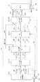
A first embodiment of the present invention will be described. FIG. 1 is a block diagram of an RGMII
RGMIIネットワークシステム1は、データ出力調整装置2Aにパーソナルコンピュータやプリンタ等の電子機器3が接続されると共に、イーサネット物理チップ(PHY)5がRGMIIインターフェースにより接続されている。電子機器3やPHY5は、データ出力調整装置2Aに対して外部装置となる。 In the RGMII
電子機器3は、メイン制御部(制御部)3Aと省エネ制御部(制御部)3Bとを備え、メイン制御部3Aのみが動作することにより全ての機能が動作する状態(以下、通常モード)と、省エネ制御部3Bのみが動作する動作する状態(以下、省エネモード)との2状態をとる。メイン制御部3Aや省エネ制御部3Bの停止や動作は、これらに電源が供給されるか否かにより制御されるが、メイン制御部3Aへの電源供給が停止する際には、このメイン制御部3Aに記憶されている種々の設定情報が失われないように設定情報の待避が行われ、又は、設定情報を記憶する記憶手段だけは動作するように設定されている。 The
なお、本実施形態においては、データ出力調整装置2A、メイン制御部3A、省エネ制御部3B、PHY5は、それぞれ独立した半導体チップにより形成されている場合について説明する。 In the present embodiment, the case where the data output adjusting
このような外部装置3は、所定時間通信が行われない場合等の予め設定された省エネモード移行条件が満たされると、通常モードから省エネモードに移行する。一方、メイン制御部3Aが省エネモードの状態であるときに、通信要求を受信する等の予め設定された復帰条件が満たされると、省エネ制御部3Bからの電源制御信号G3がメイン制御部3Aに出力されて、当該メイン制御部3Aは通常モードに復帰する。 Such an
省エネモードへの移行時及び通常モードへの復帰時において、メイン制御部3Aは、データ出力調整装置2Aにスイッチ切替信号G1を出力する。このデータ出力調整装置2Aはスイッチ切替信号G1を受信すると、後述するように通信経路切替を行う。 At the time of shifting to the energy saving mode and returning to the normal mode, the
なお、復帰条件はメイン制御部3Aが起動しなければならない、本来の処理(「例えば電子機器がプリンタである場合にはプリント処理)が要求されたときに満たされるが、ARPパケット(Adress Resolution Protcol)のように省エネ制御部3Bだけでも応答できる場合には、復帰条件に含めないことも可能である。 The return condition is satisfied when an original process (for example, print process when the electronic device is a printer) is requested, which must be activated by the
また、メイン制御部3Aは、PHY5を介してクロック信号(MDC_CLK)G5に同期してPHY5からMDIO(Management Data Input/Output)信号G4を受信する。これにより、メイン制御部3Aは、通信速度に関する情報を取得する。メイン制御部3Aは、取得した通信速度に基づき、速度選択信号G2をデータ出力調整装置2Aに出力する。データ出力調整装置2Aは、後述するように、速度選択信号G2に基づき出力データのタイミング調整を行う。 Further, the
さて、メイン制御部3Aが省エネモードと通常モードとのモード移行する際に、データ出力調整装置2Aは通信路切替を行う。このようなデータ出力調整装置2Aは、入力部21、出力部22、バッファ部23、経路切替部24を含んでいる。 Now, when the
入力部21は、メイン制御部3Aからのデータが入力するメイン側入力部21a、省エネ制御部3Bからのデータが入力する省エネ側入力部21b、PHY5からのデータが入力するPHY側入力部21cを含んでいる。 The
出力部22は、メイン制御部3Aにデータを出力するメイン側出力部22a、省エネ制御部3Bにデータを出力する省エネ側出力部22b、PHY5にデータを出力するPHY側出力部22cを含んでいる。 The
バッファ部23は、メイン側入力部21aからのデータをバッファしてPHY側出力部22cに出力するメイン側バッファ部23a、省エネ側入力部21bからのデータをバッファしてPHY側出力部22cに出力する省エネ側バッファ部23b、PHY側入力部21cからのデータをバッファしてメイン側出力部22a又は省エネ側出力部22bに出力するPHY側バッファ部23cを含んでいる。 The
また、経路切替部24は、メイン側バッファ部23a、省エネ側バッファ部23b及びPHY側出力部22cに接続されたTXスイッチ24a、メイン側出力部22a、省エネ側出力部22b及び、PHY側バッファ部23cに接続されたRXスイッチ24bを含んでいる。 The
そして、通常モードの場合には、TXスイッチ24aはメイン側バッファ部23aからのデータがPHY側出力部22cに出力されるように通信経路切替を行い(TX通信)、RXスイッチ24bはPHY側バッファ部23cからのデータがメイン側出力部22aに出力されるように通信経路切替を行う(RX通信)。 In the normal mode, the
また、省エネモードの場合には、TXスイッチ24aは省エネ側バッファ部23bからのデータがPHY側出力部22cに出力されるように通信経路切替を行い(TX通信)、RXスイッチ24bはPHY側バッファ部23cからのデータが省エネ側出力部22bに出力されるように通信経路切替を行う(RX通信)。 In the energy saving mode, the
これにより、通常モードにおけるTX通信においては、メイン制御部3Aからのデータは、メイン側入力部21a、メイン側バッファ部23a、TXスイッチ24a、PHY側出力部22cを介してPHY5に出力される。また、通常モードにおけるRX通信においては、TXスイッチ24aの動作と同時に、PHY5からのデータは、PHY側入力部21c、PHY側バッファ部23c、RXスイッチ24b、メイン側出力部22aを介してメイン制御部3Aに出力される。 Thus, in TX communication in the normal mode, data from the
一方、省エネモードにおけるTX通信においては、省エネ制御部3Bからのデータは、省エネ側入力部21b、省エネ側バッファ部23b、TXスイッチ24a、PHY側出力部22cを介してPHY5に出力される。また、省エネモードにおけるRX通信においては、TXスイッチ24aの動作と同時に、PHY5からのデータは、PHY側入力部21c、PHY側バッファ部23c、RXスイッチ24b、省エネ側出力部22bを介して省エネ制御部3Bに出力される。 On the other hand, in TX communication in the energy saving mode, data from the energy saving
なお、メイン側バッファ部23a、省エネ側バッファ部23b、PHY側バッファ部23cとしては、FIFO等のバッファ機能を持つ素子が用いられる。また、メイン側入力部21a、メイン側出力部22a、省エネ側入力部21b、省エネ側出力部22b、PHY側入力部21c、PHY側出力部22cは、データ転送等を行う際、同期用のクロック信号の立ち上がり・立ち下がりの両方を利用して処理を行うダブルデータレート(DDR)方式が用いられる。 In addition, as the main
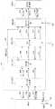
次に、通常モードを説明する。この場合、TXスイッチ24aおよびRXスイッチ24bは、スイッチ切替信号G1によりメイン制御部3AとPY5との通信路が成立するように回路接続している。図2は、通常モードにおけるTX通信を説明するブロック図である。 Next, the normal mode will be described. In this case, the
メイン制御部3Aは、TXクロック信号(TX_CLK)201、TXデータ(TX_D)202、TX制御信号(TX_CTRL)203をメイン側入力部21aに出力する。このTXクロック信号201は、データ出力調整装置2Aへのクロック信号で、イーサネットの通信速度に応じて125MHz、25MHz、2.5MHzのいずれかの周波数に設定される。無論、本発明は、他の周波数に設定されることを除くものではない。TXデータ202はデータ信号であり、TX制御信号203はデータ出力調整装置2Aへの制御信号である。 The
バス幅は、TXデータ202が4bit、TX制御信号203が1bitであり、TXデータ202の形式はイーサネットの規格に準拠している。 The bus width is 4 bits for the
また、TXデータ202とTX制御信号203とは、TXクロック信号201の立ち上がりと、立ち下がりとの両方のタイミングに同期して出力される。これにより、RGMIIの規定により通信速度が10BASE−Tと100BASE−TXとの場合、TXデータ202は、TXクロック信号201の立ち上がりと立ち下がりとで、同じデータとなる。 The
メイン側入力部21aは、メイン制御部3Aから受信したTXデータ202を、TXクロック信号201の立ち上がりと、立ち下がりとのエッジに同期して、バス幅が倍でTXクロック信号204の立ち上がりに同期した通信データ205に変換する。これにより、4bitのTXデータ202は8bitの通信データ205にビット変換され、1bitのTX制御信号203は2bitの通信制御信号206にビット変換される。 The main-
メイン側バッファ部23aは、通信データ205と通信制御信号206とをバッファリングする。そして、125MHz固定のリファレンスクロック信号(REF_CLK)207に同期して、バッファリングしている通信データ208を出力する。 The
なお、通信データ208の出力は、リファレンスクロック信号207におけるパルス毎に出力されるとは限らない。即ち、通信データ208は、リファレンスクロック信号207に同期しているが、通信速度に基づく入出力制御信号210によって125MHzの周期で出力されない場合がある。 Note that the output of the
この出力タイミングについては後述するが、メイン側バッファ部23aがリファレンスクロック信号207に同期し、かつ、入出力制御信号210により出力タイミングが制御されることにより、Giga−Etherの仕様から、クロックが125MHz/25MHz/2.5MHzのいずれかに切替えられても、適正に出力することが可能になる。 Although the output timing will be described later, the main-
また、メイン側バッファ部23aは、TXスイッチ24aを介してPHY側出力部22cに入出力状態信号211を出力する。この入出力状態信号211は、メイン側バッファ部23aにおける通信データ208のバッファ状態を通知する信号である。即ち、出力できる通信データ208がバッファされているか否かを示す信号である。 Further, the main
TXスイッチ24aは、スイッチ切替信号G1により、通常モードと省エネモードとの通信経路切替を行う。通常モードに通信経路切替された場合には、メイン側バッファ部23aとPHY側出力部との間の通信経路が成立する。TXスイッチ24aは、単純に通信経路切替を行なうだけであるので、通信データ208と通信データ212、通信制御信号209と通信制御信号213、入出力制御信号210と入出力制御信号214、入出力状態信号211と入出力状態信号215は、それぞれ同じ信号となる。 The
PHY側出力部22cは、RGMIIインターフェースの規格に適合するように、リファレンスクロック信号207の立ち上がりに同期して、通信データ212と通信制御信号213とをTXクロック信号218の立ち上がりと立ち下がりの両エッジに同期するTXデータ219とTX制御信号220とに変換して出力する。これにより、8bitの通信データ212は4bitのTXデータ219にビット変換され、2bitの通信制御信号213は1bitのTX制御信号220にビット変換される。従って、データがPHY側出力部22cから出力される速度は、メイン側バッファ部23aにバッファされる速度より遅いので、PHY側出力部22cのデータ出力タイミングに応じて、メイン側バッファ部23aからデータを受け取ることが可能になる。 The PHY
また、PHY側出力部22cには、メイン制御部3Aから速度選択信号G2が入力している。PHY側出力部22cは、この速度選択信号G2に基づき1000BASE−T、100BASE−TX、10BASE−Tのいずれの規格に従う通信速度であるかを判断し、その判断結果に基づき入出力制御信号214及びTXクロック信号218を出力する。例えば、速度選択信号G2に基づき100BASE−TXに従う通信速度であると判断した場合には、1/5の通信速度でデータの出力が行えるように、125MHz固定のリファレンスクロック信号207の5クロックで1クロックの入出力制御信号214を出力する。また、25(=125/5)MHzのTXクロック信号218を出力する。 Further, the speed selection signal G2 is input from the
そして、TXクロック信号218に同期してPHY側出力部22cから通信データ219が出力される。一方、入出力制御信号214はTXスイッチ24aを介して入出力制御信号210となって、メイン側バッファ部23aに入力する。メイン側バッファ部23aは、この入出力制御信号210に同期してバッファしている通信データ208を出力する。 Then,
以上により、メイン制御部3AとPHY5とにおけるTX通信は、データ出力調整装置2Aの有無にかかわらず同じように行える。また、メイン側バッファ部23aは、PHY側出力部22cより高速にデータがバッファされるので、PHY側出力部22cからのデータ要求に対して直ちに応じることができる。従って、データの出力タイミングが調整できる。 As described above, TX communication between the
通常モードにおけるRXスイッチ24bを介したRX通信も、上述したTX通信と同様に行われる。図3は、通常モードにおけるRX通信を説明するブロック図である。メイン側入力部21aとPHY側入力部21c、メイン側バッファ部23aとPHY側バッファ部23c、TXスイッチ24aとRXスイッチ24b、メイン側出力部22aとPHY側出力部22cがそれぞれ同じように機能して、各種の信号はPHY5からメイン制御部3Aに伝送される。 RX communication via the
これにより、PHY5とメイン制御部3AのRX通信はデータ出力調整装置2Aを介した場合も、データ出力調整装置2Aを介さない場合と同等のデータ通信を行うことができる。 Thereby, RX communication between the
図4は、省エネモードにおけるTX通信を説明するブロック図である。また、図5は、省エネモードにおけるRX通信を説明するブロック図である。これらの図から解るように、各種の信号の流れの向きが異なるが、通信機能は通常モードのTX通信と同じであるので、重複説明を省略する。 FIG. 4 is a block diagram illustrating TX communication in the energy saving mode. FIG. 5 is a block diagram for explaining RX communication in the energy saving mode. As can be seen from these figures, although the direction of the flow of various signals is different, the communication function is the same as that of the TX communication in the normal mode, and thus the duplicate description is omitted.
次に、図6に示す通常モードに設定する際のシーケンスを説明する。 Next, a sequence for setting the normal mode shown in FIG. 6 will be described.
ステップSA1: メイン制御部3Aは、データ出力調整装置2Aにおけるメイン側入力部21a、省エネ側出力部22b等の各入出力部をリセットする(ステップSA1)。 Step SA1: The
ステップSA2: そして、メイン制御部3Aは、PHY5からMDIO信号G4を受信することにより通信速度を取得し、この通信速度に基づき速度選択信号G2をメイン側出力部22a、省エネ側出力部22b、PHY側出力部22cに出力する。メイン側出力部22a等の各出力部は、この速度選択信号G2に基づきデータ出力タイミングが通信速度に適するように速度設定を行う。 Step SA2: The
ステップSA3: また、メイン制御部3Aは、ネットワーク通信に必要なIPアドレス等のパラメータを自己設定する。 Step SA3: Further, the
ステップSA4: 以上で、メイン制御部3Aは通信可能な状態になるので、スイッチ切替信号G1をデータ出力調整装置2Aに出力する。データ出力調整装置2AのTXスイッチ24a,RXスイッチ24bは、スイッチ切替信号G1に基づき通常モードに通信経路切替を行う。これにより、メイン制御部3AとPHY5とは設定された速度で通信できるようになる。 Step SA4: Since the
次に、図7に示す通常モードから省エネモードへの移行シーケンスを説明する。 Next, a transition sequence from the normal mode to the energy saving mode shown in FIG. 7 will be described.
ステップSB1: 所定の省エネ移行条件が満たされると、省エネ制御部3Bに省エネ情報が設定される。この省エネ情報は、省エネ状態においてネットワークを介しての要求があった場合に、メイン制御部3Aを起動させなくても応答できる情報(例えば、IPアドレス)である。従って、このような場合には通常モードへの復帰が行われないので、効果的な省エネが可能になる。 Step SB1: When a predetermined energy saving transition condition is satisfied, energy saving information is set in the energy saving
ステップSB2: 次に、メイン制御部3Aは、スイッチ切替信号G1をデータ出力調整装置2Aに出力する。データ出力調整装置2AのTXスイッチ24a,RXスイッチ24bは、スイッチ切替信号G1に基づき通常モードに通信経路切替を行う。これにより、省エネ制御部3BとPHY5とは設定された速度で通信できるようになる。 Step SB2: Next, the
ステップSB3: 以上で、省エネモードに移行する準備が整ったので、省エネ制御部3Bは、メイン制御部3Aの電源をOFFにする電源制御信号G3を出力する。これにより、メイン制御部3Aへの電源供給が停止する。 Step SB3: Since preparation for shifting to the energy saving mode is completed as described above, the energy saving
次に、図8に示す省エネモードから通常モードへの復帰シーケンスを説明する。 Next, a return sequence from the energy saving mode to the normal mode shown in FIG. 8 will be described.
ステップSC1: 省エネモードにおいて、省エネ制御部3Bがネットワーク通信を行なった結果、メイン制御部3Aの起動が必要と判断した場合には、メイン制御部3Aの電源供給を開始する電源制御信号G3が出力される。これにより、メイン制御部3Aが起動する。 Step SC1: In the energy saving mode, when it is determined that the
ステップSC2〜SC4: そして、メイン制御部3Aは、データ出力調整装置2Aに各入出力部のリセットを行なわせると共に、PHY5から通信速度を読取り、速度選択信号G2を出力する。データ出力調整装置2Aの各入出力部は、速度選択信号G2に基づき速度設定を行う。また、メイン制御部3AはIPアドレス等の設定情報を自機に設定する。 Steps SC2 to SC4: Then, the
ステップSC5: 次に、メイン制御部3Aは、スイッチ切替信号G1をデータ出力調整装置2Aに出力する。データ出力調整装置2AにおけるTXスイッチ24a、RXスイッチ24bは、スイッチ切替信号G1に基づき通常モードに通信経路切替を行う。これにより、通常モードに復帰する。 Step SC5: Next, the
以上説明したように、経路切替部24でネットワーク切替を行うため、複数の速度の通信に対してもデータの出力調整しながら通信できるようになる。また、かかる複数の速度の通信が行われる場合であっても、省エネモードを実現することができる。
<第2の実施形態>
次に、本発明の第2の実施形態を説明する。なお、第1の実施形態と同一構成に関しては、同一符号を用いて説明を適宜省略する。As described above, since the network is switched by the
<Second Embodiment>
Next, a second embodiment of the present invention will be described. In addition, about the same structure as 1st Embodiment, description is abbreviate | omitted suitably using the same code | symbol.
第1の実施形態においては、メイン制御部3A、省エネ制御部3B、PHY部5及び、データ出力調整装置2Aは、それぞれ独立したチップで構成した。これに対し、本実施形態では、省エネ制御部3Bとデータ出力調整装置2Aとを1つのチップに纏めて構成した。以下、省エネ制御部とデータ出力調整装置とを纏めてネットワーク応答回路と記載する。 In the first embodiment, the
図9は、本第2の実施形態にかかるネットワーク応答回路を備えたRGMIIネットワークシステムのブロック図である。図1に対し、省エネ制御部3Bとデータ出力調整装置2Bとが纏められて、ネットワーク応答回路6を構成している。このような構成においては、省エネ制御部3Bとデータ出力調整装置2Bとの接続がチップの内部配線を用いて行えるので、これらの間のインターフェースが不要となる。従って、第1の実施形態において説明した省エネ制御部3Bにおける省エネ側入力部21b及び省エネ側出力部22bは、省略できる。 FIG. 9 is a block diagram of an RGMII network system including a network response circuit according to the second embodiment. With respect to FIG. 1, the energy saving
また、このネットワーク応答回路6にはレジスタ制御部7が設けられ、メイン制御部3Aからの信号を記憶し、記憶した内容に従って速度選択信号G2及びスイッチ切替信号G1が出力されるようになっている。従って、メイン制御部3Aが省エネモードであるか通常モードであるかにかかわらず、データ出力調整装置2Bにおけるモード切替が行うことができる。このことは、省エネモードへの移行の準備が未完了な場合でも、メイン制御部3Aがレジスタ制御部7に速度選択信号G2やスイッチ切替信号G1の基となる指令信号G7を出力すると、直ちに停止状態となることができることを意味し、効率的な省エネを行うことが可能になる。 Further, the network response circuit 6 is provided with a register control unit 7, which stores a signal from the
なお、省エネ制御部3Bは、CPU(中央演算装置)によるプログラム処理が可能な制御だけでなく、規定のネットワークパケットに応答及び規定のネットワークパケット復帰を検出するようにしてもよい。 Note that the energy saving
また、省エネ制御部3Bの接続を、例えば10BASE−T/100BASE−TXに制限し、MII(Media Independent Interface)など他のインターフェースにした場合も同様に適用可能である。この場合、ネットワーク応答回路6のチップに組み込まれた省エネ制御部3B又はネットワーク応答回路6に入力されるデータはPHY側バッファ部23cを通過しリファレンスクロック信号で125MHzに統一されたものでなくてもよい。 In addition, the connection of the energy saving
1 RGMIIネットワークシステム
2A,2B データ出力調整装置
3 電子機器(外部装置)
3A メイン制御部
3B 省エネ制御部
5 PHY
6 ネットワーク応答回路
7 レジスタ制御部
21 入力部
21a メイン側入力部
21b 省エネ側入力部
21c PHY側入力部
22 出力部
22a メイン側出力部
22b 省エネ側出力部
22c PHY側出力部
23 バッファ部
23a メイン側バッファ部
23b 省エネ側バッファ部
23c PHY側バッファ部
24 経路切替部
24a TXスイッチ
24b RXスイッチ1
3A
6 Network response circuit 7
Claims (5)
Translated fromJapanese前記外部装置に対応して設けられて、前記外部装置からのデータを取り込んでビット変換して出力する入力部と、
前記入力部に対応して設けられて、前記入力部からのビット変換された前記データをバッファするバッファ部と、
前記バッファ部に通信速度に応じて前記データを出力する際の出力タイミングを指示し、この指示に従い当該バッファ部が所定周波数に固定されたクロック信号に同期して出力したビット変換された前記データを受信して、他の前記外部装置に出力する出力部と、
を備えることを特徴とするデータ出力調整装置。A data output adjustment device thatis provided between a plurality of external devices and adjusts output timing when datainput from theexternal device is output toanother external device at a different communication speed,
Said provided corresponding to the external device, an input unitfor data bit conversion Nde Capturesoutput from the external device,
A buffer unit provided corresponding to the input unit and buffering thebit-converted data from the input unit;
The buffer unit is instructed to output timing when outputting the data accordingto the communication speed, and thebit-converted data output by the buffer unitin synchronization with a clock signal fixed at a predetermined frequency in accordance with this instruction. An output unit that receives and outputs to the other external device;
A data output adjusting device comprising:
前記外部装置からのデータを取り込んでデータの取り込み、これをビット変換して出力する入力手順と、
前記入力部からのビット変換された前記データを取り込んでバッファするバッファ手順と、
前記バッファ部に通信速度に応じて前記データを出力する際の出力タイミングを出力するタイミング指示手順と、 前記タイミング指示手順に従い前記バッファ部が所定周波数に固定されたクロック信号に同期して出力したビット変換された前記データを受信して、他の前記外部装置に出力する出力手順と、
を含むことを特徴とするデータ出力調整方法。A data output adjustment method for adjusting data output, which is provided between a plurality of external devices and adjusts output timing when data input from the external device is output to another external device at a different communication speed,
An input procedurefor taking in datafrom the external device, taking in the data,and converting it into bits and outputting it,
A buffer procedure fortaking in and buffering thebit-converted data from the input unit;
A timing instruction procedure for outputting an output timing when the data is output to thebuffer unit according to a communication speed, and abit output by the buffer unitin synchronization with a clock signal fixed at a predetermined frequency according to the timing instruction procedure An output procedure for receiving theconverted data and outputting it to the other external device;
A method for adjusting data output, comprising:
所定の処理を行う第1の外部装置と、
前記RGMIIネットワークに接続されるイーサネット物理層を含む第2の外部装置と、
前記第1の外部装置が省エネ状態に移行した際に動作する第3の外部装置と、
前記第1の外部装置と第2の外部装置に対応して設けられた請求項1に記載のデータ出力調整装置、及び、前記データ出力調整装置を介して前記外部装置が相互に1対1で通信するための通信路を設定するスイッチを含む経路切替部と、
を備え、
前記第1の外部装置が行う所定の処理には、前記RGMIIネットワークを介して行われる通信の通信速度を検出して、当該通信速度を示す速度選択信号を前記データ出力調整装置における出力部に指示する処理と、
前記通信路を設定するためのスイッチ切替信号を前記経路切替部に指示する処理とが、含まれて、
前記データ出力調整装置における出力部は、前記速度選択信号に基づき当該データ出力調整装置におけるバッファ部に前記データの出力タイミングを指示し、前記経路切替部は、前記スイッチ切替信号に基づき前記通信路を切り替え、かつ、前記出力部は、前記出力タイミングに従い前記バッファ部が所定周波数に固定されたクロック信号に同期して出力した前記データを受信して、他の前記外部装置に出力することを特徴とするRGMIIネットワークネットワークシステム。An RGMII network system for performing communication via an RGMII network,
A first external device for performing predetermined processing;
A second external device including an Ethernet physical layer connected to the RGMII network;
A third external device that operates when the first external device shifts to an energy saving state;
The data output adjustment device according toclaim 1 provided corresponding to the first external device and the second external device, and the external devices are in a one-to-one relationship with each other via the data output adjustment device. A path switching unit including a switch for setting a communication path for communication;
With
In the predetermined processing performed by the first external device, a communication speed of communication performed via the RGMII network is detected, and a speed selection signal indicating the communication speed is instructed to an output unit in the data output adjustment device Processing to
And a process of instructing the path switching unit to provide a switch switching signal for setting the communication path,
The output unit in the data output adjusting device instructs the output timing of the data to the buffer unit in the data output adjusting device based on the speed selection signal, and the path switching unit sets the communication path based on the switch switching signal. switching,and the output section is the buffer unit in accordance with the output timing to receive the data output in synchronization with the fixed clock signal to a predetermined frequency, wherein alsobe output fromthe other of said external device RGMII network network system.
前記データ出力調整装置は、前記第3の外部装置に対応しても設けられていることを特徴とするRGMIIネットワークシステム。The RGMII network system according to claim 3,
The RGMII network system, wherein the data output adjustment device is also provided corresponding to the third external device.
通信速度を検出する手順と、
データを入力する入力手順と、
入力したデータをバッファするバッファ手順と、
前記通信速度に応じて出力する前記データの出力タイミングを指示するタイミング指示手順と、
前記タイミング指示手順に従い前記バッファ部が所定周波数に固定されたクロック信号に同期して出力した前記データを受信して、他の前記外部装置に出力する出力された前記データを出力する出力手順と、
を含むことを特徴とするRGMIIネットワーク通信路切替方法。An RGMII network communication path switching method for switching a communication path when communicating via an RGMII network,
A procedure for detecting the communication speed;
Input procedure to input data,
A buffering procedure to buffer the entered data;
A timing instruction procedure for instructing an output timing of the data to be output according to the communication speed;
An output procedurefor receiving the data output in synchronization with a clock signal fixed to a predetermined frequency by the buffer unit according to the timing instruction procedure,and outputting the output data to be output toanother external device ;
An RGMII network communication path switching method comprising:
Priority Applications (2)
| Application Number | Priority Date | Filing Date | Title |
|---|---|---|---|
| JP2011124400AJP5902402B2 (en) | 2011-06-02 | 2011-06-02 | Data output adjustment device, data output adjustment method, RGMII network system, and RGMII network communication path switching method |
| US13/486,919US8831017B2 (en) | 2011-06-02 | 2012-06-01 | Data output adjustment apparatus, data output adjustment method, RGMII network system and RGMII network communication path change method |
Applications Claiming Priority (1)
| Application Number | Priority Date | Filing Date | Title |
|---|---|---|---|
| JP2011124400AJP5902402B2 (en) | 2011-06-02 | 2011-06-02 | Data output adjustment device, data output adjustment method, RGMII network system, and RGMII network communication path switching method |
Publications (2)
| Publication Number | Publication Date |
|---|---|
| JP2012253555A JP2012253555A (en) | 2012-12-20 |
| JP5902402B2true JP5902402B2 (en) | 2016-04-13 |
Family
ID=47261644
Family Applications (1)
| Application Number | Title | Priority Date | Filing Date |
|---|---|---|---|
| JP2011124400AExpired - Fee RelatedJP5902402B2 (en) | 2011-06-02 | 2011-06-02 | Data output adjustment device, data output adjustment method, RGMII network system, and RGMII network communication path switching method |
Country Status (2)
| Country | Link |
|---|---|
| US (1) | US8831017B2 (en) |
| JP (1) | JP5902402B2 (en) |
Families Citing this family (1)
| Publication number | Priority date | Publication date | Assignee | Title |
|---|---|---|---|---|
| US20130336204A1 (en)* | 2012-06-13 | 2013-12-19 | Jen-Chieh Huang | Control method for adjusting queuing data volumn of wireless communications device by detecting data transfer speed at physical layer and related control module and machine-readable medium thereof |
Family Cites Families (20)
| Publication number | Priority date | Publication date | Assignee | Title |
|---|---|---|---|---|
| US6334219B1 (en)* | 1994-09-26 | 2001-12-25 | Adc Telecommunications Inc. | Channel selection for a hybrid fiber coax network |
| US6127970A (en)* | 1998-09-25 | 2000-10-03 | Lin; Ching-Fang | Coupled real time emulation method for positioning and location system |
| US6374288B1 (en)* | 1999-01-19 | 2002-04-16 | At&T Corp | Digital subscriber line server system and method for dynamically changing bit rates in response to user requests and to message types |
| JP2001154763A (en)* | 1999-11-30 | 2001-06-08 | Nec Shizuoka Ltd | Power saving device for local area network board |
| US6778480B2 (en)* | 2002-05-30 | 2004-08-17 | Zoran Corporation | Method and apparatus for automatic slip defect management in a DVD drive |
| US20030231660A1 (en)* | 2002-06-14 | 2003-12-18 | Bapiraju Vinnakota | Bit-manipulation instructions for packet processing |
| TWI220619B (en)* | 2003-03-03 | 2004-08-21 | Ic Plus Corp | Network physical layer with power off alerting function and alerting method thereof |
| US7373520B1 (en)* | 2003-06-18 | 2008-05-13 | Symantec Operating Corporation | Method for computing data signatures |
| JP4271520B2 (en)* | 2003-07-22 | 2009-06-03 | 株式会社リコー | Image forming apparatus |
| JP2005092764A (en)* | 2003-09-19 | 2005-04-07 | Ricoh Co Ltd | Image forming apparatus, interface board, interface chip, and information processing apparatus |
| US7929518B2 (en)* | 2004-07-15 | 2011-04-19 | Broadcom Corporation | Method and system for a gigabit Ethernet IP telephone chip with integrated DDR interface |
| US7688806B2 (en)* | 2004-07-15 | 2010-03-30 | Broadcom Corporation | Method and system for a gigabit ethernet IP telephone chip |
| US7376774B1 (en)* | 2004-08-27 | 2008-05-20 | Xilinx, Inc. | Network media access controller embedded in a programmable logic device—host interface control generator |
| JP2006293983A (en)* | 2005-03-18 | 2006-10-26 | Ricoh Co Ltd | Network communication apparatus, image forming apparatus, network communication method, and program |
| US7500051B2 (en)* | 2006-09-13 | 2009-03-03 | International Business Machines Corporation | Migration of partitioned persistent disk cache from one host to another |
| JP5309580B2 (en) | 2008-02-04 | 2013-10-09 | 沖電気工業株式会社 | Network processor |
| CN101631137B (en)* | 2008-07-15 | 2012-10-10 | 株式会社日立制作所 | Communication control device and communication control method |
| KR101569030B1 (en)* | 2009-10-14 | 2015-11-16 | 삼성전자주식회사 | Image forming apparatus and network connection method thereof |
| JP5365558B2 (en)* | 2010-03-17 | 2013-12-11 | 富士通株式会社 | Wireless network control device, wireless network control method, and wireless network control system |
| TWI466519B (en)* | 2010-11-29 | 2014-12-21 | Realtek Semiconductor Corp | Network device and network connection method |
- 2011
- 2011-06-02JPJP2011124400Apatent/JP5902402B2/ennot_activeExpired - Fee Related
- 2012
- 2012-06-01USUS13/486,919patent/US8831017B2/ennot_activeExpired - Fee Related
Also Published As
| Publication number | Publication date |
|---|---|
| JP2012253555A (en) | 2012-12-20 |
| US8831017B2 (en) | 2014-09-09 |
| US20120307835A1 (en) | 2012-12-06 |
Similar Documents
| Publication | Publication Date | Title |
|---|---|---|
| JP3827332B2 (en) | Highly integrated Ethernet network elements | |
| US10891242B2 (en) | Embedded USB2 (eUSB2) repeater operation | |
| TWI542239B (en) | Dynamic power management in a communications device | |
| JP3992100B2 (en) | Network to increase transmission link layer core speed | |
| JP2011050071A (en) | Cross point switch with serializer and deserializer function | |
| CN113424164B (en) | Power consumption reduction in USB 2.0 transfer driver and eUSB2 repeater | |
| WO2020239109A1 (en) | Mipi d-phy transmission circuit and device | |
| EP1249971B1 (en) | Network Interface Using Programmable Delay and Frequency Doubler | |
| CN105306421A (en) | PCI-E interface based signal processing method and PCI-E interface based signal processing device | |
| JP5902402B2 (en) | Data output adjustment device, data output adjustment method, RGMII network system, and RGMII network communication path switching method | |
| JP5926583B2 (en) | Information processing apparatus, serial communication system, communication initialization method thereof, and serial communication apparatus | |
| EP1525722B1 (en) | Packet signal processing architecture | |
| JP3871177B2 (en) | Data communication apparatus and data communication method | |
| JP5309580B2 (en) | Network processor | |
| JP7537769B2 (en) | Serial interface circuit, control method thereof, program, communication module, and communication device | |
| JP2013192007A (en) | Communication device, image formation device, communication system, router, communication method, and communication program | |
| KR20200062582A (en) | ethernet switch semiconductor | |
| JP4095216B2 (en) | Printer and data communication method in printer | |
| JP2003289315A (en) | Packet transfer apparatus and packet transfer method | |
| CN100433679C (en) | Seamless switching method and apparatus for communication network | |
| JP2006304011A (en) | Interface circuit | |
| EP0992914B1 (en) | Data transfer device between computer nodes | |
| JP5921264B2 (en) | Serial communication system and communication initialization method thereof, and serial communication apparatus and communication initialization method thereof | |
| JP6488756B2 (en) | Communication control apparatus and image forming apparatus | |
| JP3581112B2 (en) | Data transmission method, transmission circuit, and communication device |
Legal Events
| Date | Code | Title | Description |
|---|---|---|---|
| A621 | Written request for application examination | Free format text:JAPANESE INTERMEDIATE CODE: A621 Effective date:20140519 | |
| A711 | Notification of change in applicant | Free format text:JAPANESE INTERMEDIATE CODE: A712 Effective date:20140724 | |
| A977 | Report on retrieval | Free format text:JAPANESE INTERMEDIATE CODE: A971007 Effective date:20150311 | |
| A131 | Notification of reasons for refusal | Free format text:JAPANESE INTERMEDIATE CODE: A131 Effective date:20150324 | |
| A521 | Written amendment | Free format text:JAPANESE INTERMEDIATE CODE: A523 Effective date:20150515 | |
| A131 | Notification of reasons for refusal | Free format text:JAPANESE INTERMEDIATE CODE: A131 Effective date:20150908 | |
| TRDD | Decision of grant or rejection written | ||
| A01 | Written decision to grant a patent or to grant a registration (utility model) | Free format text:JAPANESE INTERMEDIATE CODE: A01 Effective date:20160216 | |
| A61 | First payment of annual fees (during grant procedure) | Free format text:JAPANESE INTERMEDIATE CODE: A61 Effective date:20160310 | |
| R150 | Certificate of patent or registration of utility model | Ref document number:5902402 Country of ref document:JP Free format text:JAPANESE INTERMEDIATE CODE: R150 | |
| LAPS | Cancellation because of no payment of annual fees |