JP5900614B2 - Semiconductor manufacturing equipment - Google Patents
Semiconductor manufacturing equipmentDownload PDFInfo
- Publication number
- JP5900614B2 JP5900614B2JP2014516546AJP2014516546AJP5900614B2JP 5900614 B2JP5900614 B2JP 5900614B2JP 2014516546 AJP2014516546 AJP 2014516546AJP 2014516546 AJP2014516546 AJP 2014516546AJP 5900614 B2JP5900614 B2JP 5900614B2
- Authority
- JP
- Japan
- Prior art keywords
- substrate
- chamber
- substrate holder
- semiconductor manufacturing
- manufacturing apparatus
- Prior art date
- Legal status (The legal status is an assumption and is not a legal conclusion. Google has not performed a legal analysis and makes no representation as to the accuracy of the status listed.)
- Expired - Fee Related
Links
Images


Classifications
- C—CHEMISTRY; METALLURGY
- C23—COATING METALLIC MATERIAL; COATING MATERIAL WITH METALLIC MATERIAL; CHEMICAL SURFACE TREATMENT; DIFFUSION TREATMENT OF METALLIC MATERIAL; COATING BY VACUUM EVAPORATION, BY SPUTTERING, BY ION IMPLANTATION OR BY CHEMICAL VAPOUR DEPOSITION, IN GENERAL; INHIBITING CORROSION OF METALLIC MATERIAL OR INCRUSTATION IN GENERAL
- C23C—COATING METALLIC MATERIAL; COATING MATERIAL WITH METALLIC MATERIAL; SURFACE TREATMENT OF METALLIC MATERIAL BY DIFFUSION INTO THE SURFACE, BY CHEMICAL CONVERSION OR SUBSTITUTION; COATING BY VACUUM EVAPORATION, BY SPUTTERING, BY ION IMPLANTATION OR BY CHEMICAL VAPOUR DEPOSITION, IN GENERAL
- C23C16/00—Chemical coating by decomposition of gaseous compounds, without leaving reaction products of surface material in the coating, i.e. chemical vapour deposition [CVD] processes
- C23C16/44—Chemical coating by decomposition of gaseous compounds, without leaving reaction products of surface material in the coating, i.e. chemical vapour deposition [CVD] processes characterised by the method of coating
- C23C16/46—Chemical coating by decomposition of gaseous compounds, without leaving reaction products of surface material in the coating, i.e. chemical vapour deposition [CVD] processes characterised by the method of coating characterised by the method used for heating the substrate
- C—CHEMISTRY; METALLURGY
- C23—COATING METALLIC MATERIAL; COATING MATERIAL WITH METALLIC MATERIAL; CHEMICAL SURFACE TREATMENT; DIFFUSION TREATMENT OF METALLIC MATERIAL; COATING BY VACUUM EVAPORATION, BY SPUTTERING, BY ION IMPLANTATION OR BY CHEMICAL VAPOUR DEPOSITION, IN GENERAL; INHIBITING CORROSION OF METALLIC MATERIAL OR INCRUSTATION IN GENERAL
- C23C—COATING METALLIC MATERIAL; COATING MATERIAL WITH METALLIC MATERIAL; SURFACE TREATMENT OF METALLIC MATERIAL BY DIFFUSION INTO THE SURFACE, BY CHEMICAL CONVERSION OR SUBSTITUTION; COATING BY VACUUM EVAPORATION, BY SPUTTERING, BY ION IMPLANTATION OR BY CHEMICAL VAPOUR DEPOSITION, IN GENERAL
- C23C14/00—Coating by vacuum evaporation, by sputtering or by ion implantation of the coating forming material
- C23C14/22—Coating by vacuum evaporation, by sputtering or by ion implantation of the coating forming material characterised by the process of coating
- C23C14/54—Controlling or regulating the coating process
- C23C14/541—Heating or cooling of the substrates
- C—CHEMISTRY; METALLURGY
- C23—COATING METALLIC MATERIAL; COATING MATERIAL WITH METALLIC MATERIAL; CHEMICAL SURFACE TREATMENT; DIFFUSION TREATMENT OF METALLIC MATERIAL; COATING BY VACUUM EVAPORATION, BY SPUTTERING, BY ION IMPLANTATION OR BY CHEMICAL VAPOUR DEPOSITION, IN GENERAL; INHIBITING CORROSION OF METALLIC MATERIAL OR INCRUSTATION IN GENERAL
- C23C—COATING METALLIC MATERIAL; COATING MATERIAL WITH METALLIC MATERIAL; SURFACE TREATMENT OF METALLIC MATERIAL BY DIFFUSION INTO THE SURFACE, BY CHEMICAL CONVERSION OR SUBSTITUTION; COATING BY VACUUM EVAPORATION, BY SPUTTERING, BY ION IMPLANTATION OR BY CHEMICAL VAPOUR DEPOSITION, IN GENERAL
- C23C16/00—Chemical coating by decomposition of gaseous compounds, without leaving reaction products of surface material in the coating, i.e. chemical vapour deposition [CVD] processes
- C23C16/44—Chemical coating by decomposition of gaseous compounds, without leaving reaction products of surface material in the coating, i.e. chemical vapour deposition [CVD] processes characterised by the method of coating
- C23C16/50—Chemical coating by decomposition of gaseous compounds, without leaving reaction products of surface material in the coating, i.e. chemical vapour deposition [CVD] processes characterised by the method of coating using electric discharges
- H—ELECTRICITY
- H01—ELECTRIC ELEMENTS
- H01L—SEMICONDUCTOR DEVICES NOT COVERED BY CLASS H10
- H01L21/00—Processes or apparatus adapted for the manufacture or treatment of semiconductor or solid state devices or of parts thereof
- H01L21/67—Apparatus specially adapted for handling semiconductor or electric solid state devices during manufacture or treatment thereof; Apparatus specially adapted for handling wafers during manufacture or treatment of semiconductor or electric solid state devices or components ; Apparatus not specifically provided for elsewhere
- H01L21/67005—Apparatus not specifically provided for elsewhere
- H01L21/67011—Apparatus for manufacture or treatment
- H01L21/67098—Apparatus for thermal treatment
- H01L21/67109—Apparatus for thermal treatment mainly by convection
- H—ELECTRICITY
- H01—ELECTRIC ELEMENTS
- H01L—SEMICONDUCTOR DEVICES NOT COVERED BY CLASS H10
- H01L21/00—Processes or apparatus adapted for the manufacture or treatment of semiconductor or solid state devices or of parts thereof
- H01L21/67—Apparatus specially adapted for handling semiconductor or electric solid state devices during manufacture or treatment thereof; Apparatus specially adapted for handling wafers during manufacture or treatment of semiconductor or electric solid state devices or components ; Apparatus not specifically provided for elsewhere
- H01L21/67005—Apparatus not specifically provided for elsewhere
- H01L21/67011—Apparatus for manufacture or treatment
- H01L21/67098—Apparatus for thermal treatment
- H01L21/67115—Apparatus for thermal treatment mainly by radiation
- H—ELECTRICITY
- H01—ELECTRIC ELEMENTS
- H01L—SEMICONDUCTOR DEVICES NOT COVERED BY CLASS H10
- H01L21/00—Processes or apparatus adapted for the manufacture or treatment of semiconductor or solid state devices or of parts thereof
- H01L21/67—Apparatus specially adapted for handling semiconductor or electric solid state devices during manufacture or treatment thereof; Apparatus specially adapted for handling wafers during manufacture or treatment of semiconductor or electric solid state devices or components ; Apparatus not specifically provided for elsewhere
- H01L21/67005—Apparatus not specifically provided for elsewhere
- H01L21/67011—Apparatus for manufacture or treatment
- H01L21/67155—Apparatus for manufacturing or treating in a plurality of work-stations
- H01L21/67161—Apparatus for manufacturing or treating in a plurality of work-stations characterized by the layout of the process chambers
- H01L21/67173—Apparatus for manufacturing or treating in a plurality of work-stations characterized by the layout of the process chambers in-line arrangement
- H—ELECTRICITY
- H01—ELECTRIC ELEMENTS
- H01L—SEMICONDUCTOR DEVICES NOT COVERED BY CLASS H10
- H01L21/00—Processes or apparatus adapted for the manufacture or treatment of semiconductor or solid state devices or of parts thereof
- H01L21/67—Apparatus specially adapted for handling semiconductor or electric solid state devices during manufacture or treatment thereof; Apparatus specially adapted for handling wafers during manufacture or treatment of semiconductor or electric solid state devices or components ; Apparatus not specifically provided for elsewhere
- H01L21/673—Apparatus specially adapted for handling semiconductor or electric solid state devices during manufacture or treatment thereof; Apparatus specially adapted for handling wafers during manufacture or treatment of semiconductor or electric solid state devices or components ; Apparatus not specifically provided for elsewhere using specially adapted carriers or holders; Fixing the workpieces on such carriers or holders
- H01L21/67326—Horizontal carrier comprising wall type elements whereby the substrates are vertically supported, e.g. comprising sidewalls
Landscapes
- Engineering & Computer Science (AREA)
- Chemical & Material Sciences (AREA)
- Physics & Mathematics (AREA)
- Condensed Matter Physics & Semiconductors (AREA)
- General Physics & Mathematics (AREA)
- Manufacturing & Machinery (AREA)
- Computer Hardware Design (AREA)
- Microelectronics & Electronic Packaging (AREA)
- Power Engineering (AREA)
- Materials Engineering (AREA)
- Chemical Kinetics & Catalysis (AREA)
- Mechanical Engineering (AREA)
- Metallurgy (AREA)
- Organic Chemistry (AREA)
- General Chemical & Material Sciences (AREA)
- Health & Medical Sciences (AREA)
- Toxicology (AREA)
- Plasma & Fusion (AREA)
- Chemical Vapour Deposition (AREA)
- Physical Vapour Deposition (AREA)
Description
Translated fromJapanese本発明は、基板の加熱処理を含む半導体製造工程に使用される半導体製造装置に関する。 The present invention relates to a semiconductor manufacturing apparatus used in a semiconductor manufacturing process including heat treatment of a substrate.
半導体製品の製造工程において基板を加熱処理する方法として、成膜処理やエッチング処理などの処理を行う処理チャンバー内で基板を加熱する方法と、加熱チャンバーで予備加熱した基板を処理チャンバーに搬入するインライン式製造装置を使用する方法がある。 As a method for heat-treating a substrate in a manufacturing process of a semiconductor product, a method of heating a substrate in a processing chamber for performing a film forming process or an etching process, and an in-line in which a substrate preheated in a heating chamber is carried into the processing chamber. There is a method of using a type manufacturing apparatus.
例えば太陽電池反射防止膜の成膜処理などでは、処理対象の基板の温度を予め決められた設定温度にした状態で、基板に膜を形成する。このため、インライン式成膜装置で成膜処理する場合には、成膜処理用の処理チャンバーに搬入される前に、基板は加熱チャンバー内で予備加熱される。そして、設定温度に達した基板が成膜チャンバーに搬入され、成膜処理が行われる(例えば、特許文献1参照。)。 For example, in the film formation process of the solar cell antireflection film, the film is formed on the substrate in a state where the temperature of the substrate to be processed is set to a predetermined set temperature. For this reason, in the case of performing a film forming process using an in-line film forming apparatus, the substrate is preheated in the heating chamber before being carried into the film forming process chamber. Then, the substrate that has reached the set temperature is carried into a film formation chamber, and a film formation process is performed (see, for example, Patent Document 1).
半導体製造装置では、時間当たりの基板処理枚数が重要な性能である。このため、基板の加熱時間を短縮して、1枚当たりの処理時間を短くする必要がある。加熱時間短縮のためにはランプヒータなどの高パワーのヒータを使用し、基板の昇温レートを高くすることが一般には有効である。特に結晶性シリコンの太陽電池の反射防止膜を形成する成膜装置では、成膜時の基板温度を400℃以上という高温にする必要があるため、時間当たりの基板処理枚数を増やすために高い昇温レートが求められている。 In a semiconductor manufacturing apparatus, the number of substrates processed per hour is an important performance. For this reason, it is necessary to shorten the substrate heating time and the processing time per one substrate. In order to shorten the heating time, it is generally effective to use a high-power heater such as a lamp heater and increase the temperature rising rate of the substrate. In particular, in a film forming apparatus for forming an antireflection film for a crystalline silicon solar cell, it is necessary to increase the substrate temperature at the time of film formation to 400 ° C. or higher. A temperature rate is required.
しかし、ヒータの熱エネルギーは、基板加熱だけではなく基板を搭載する基板ホルダやチャンバーの壁面に伝わり、更にはチャンバーの壁面を介して外気やチャンバーの冷却機構に伝わる。このような損失エネルギーが大きいと基板を加熱するために更に多くのエネルギーが必要になるという問題があった。 However, the thermal energy of the heater is transmitted not only to the substrate heating but also to the substrate holder on which the substrate is mounted and the wall surface of the chamber, and further to the outside air and the chamber cooling mechanism via the wall surface of the chamber. When such loss energy is large, there is a problem that more energy is required to heat the substrate.
また、チャンバー壁面では熱エネルギーの放熱レートが大きいため、チャンバー壁面付近に配置した基板の温度が低くなり、基板の温度均一性が確保できない。チャンバーの外側を断熱材で覆う方法があるが、大きな熱質量のあるチャンバー壁の加熱に熱エネルギーが必要になり、効率的な基板加熱とならない。また、チャンバー壁面が加熱されると、チャンバーの真空シールのために使用しているガスケットやチャンバー外側に取り付けている電子部品、樹脂部品等の温度が上昇し、それらの部品を劣化・損傷させる恐れが生じる。それらの部品の熱劣化・損傷を防ぐためにチャンバー壁を水冷や空冷で冷却することとなり、チャンバー壁への放熱がさらに増加する。これにより、エネルギー効率やチャンバー内及び基板の温度均一性は更に悪化する。 In addition, since the heat release rate of the thermal energy is large on the chamber wall surface, the temperature of the substrate disposed in the vicinity of the chamber wall surface becomes low, and the temperature uniformity of the substrate cannot be ensured. Although there is a method of covering the outside of the chamber with a heat insulating material, heat energy is required for heating the chamber wall having a large thermal mass, and the substrate cannot be efficiently heated. In addition, if the chamber wall surface is heated, the temperature of gaskets used for vacuum sealing of the chamber, electronic parts attached to the outside of the chamber, resin parts, etc. will rise, and these parts may be deteriorated or damaged. Occurs. In order to prevent thermal degradation and damage of these parts, the chamber wall is cooled by water cooling or air cooling, and heat radiation to the chamber wall is further increased. Thereby, the energy efficiency and the temperature uniformity in the chamber and the substrate are further deteriorated.
上記問題点に鑑み、本発明は、エネルギー効率の良い基板加熱処理が可能な半導体製造装置を提供することを目的とする。 In view of the above problems, an object of the present invention is to provide a semiconductor manufacturing apparatus capable of energy efficient substrate heat treatment.
本発明の一態様によれば、(イ)基板を搭載した基板ホルダを格納するチャンバーと、(ロ)チャンバーの内部に配置され、基板ホルダに搭載された基板を加熱する加熱装置と、(ハ)ファイバーで編んだ布状の外装材で内部材を包んだ構造の有機添加剤を含有していない無機材料からなり、チャンバーの内壁を覆って配置された外部断熱材と、(ニ)外部断熱材の加熱装置に対向する表面上に配置された外部熱反射板と、(ホ)基板ホルダ及び加熱装置を囲んでチャンバー内に配置された内部断熱機構とを備え、ファイバーで編んだ布状の外装材で内部材を包んだ構造の有機添加剤を含有していない無機材料からなる内部断熱材が内部断熱機構の内壁を覆って配置され、且つ、内部熱反射板が内部断熱材の加熱装置に対向する表面上に配置されている半導体製造装置が提供される。According to one aspect of the present invention, (a) a chamber for storing a substrate holder on which a substrate is mounted, (b) a heating device that is disposed inside the chamber and that is mounted on the substrate holder, and (c) An external heat insulating material that is made of an inorganic material that does not contain organic additives and has a structure in which an inner member is wrapped with a cloth-like outer material knitted with fiber; and (d) an external heat insulating material that covers the inner wall of the chamber. An external heat reflecting plate disposed on the surface facing the material heating device, and(e) an internal heat insulating mechanism disposed in the chamber surrounding the substrate holder and the heating device, and havinga cloth shape knitted withfiber An internal heat insulating material made of an inorganic material not containing an organic additive having a structure in which an inner member is wrapped with an exterior material is disposed to cover the inner wall of the internal heat insulating mechanism, and the internal heat reflecting plate is a heating device for the internal heat insulating material Placed on the surface facing The semiconductor manufacturing apparatus is providedthat is.
本発明によれば、エネルギー効率の良い基板加熱処理が可能な半導体製造装置を提供できる。 According to the present invention, it is possible to provide a semiconductor manufacturing apparatus capable of energy efficient substrate heating.
図面を参照して、本発明の第1乃至第6の実施形態を説明する。以下の図面の記載において、同一又は類似の部分には同一又は類似の符号を付している。ただし、図面は模式的なものであることに留意すべきである。又、以下に示す実施形態は、この発明の技術的思想を具体化するための装置や方法を例示するものであって、この発明の実施形態は、構成部品の構造、配置などを下記のものに特定するものでない。この発明の実施形態は、請求の範囲において、種々の変更を加えることができる。 First to sixth embodiments of the present invention will be described with reference to the drawings. In the following description of the drawings, the same or similar parts are denoted by the same or similar reference numerals. However, it should be noted that the drawings are schematic. Further, the embodiment described below exemplifies an apparatus and a method for embodying the technical idea of the present invention, and the embodiment of the present invention has the following structure and arrangement of components. It is not something specific. The embodiment of the present invention can be variously modified within the scope of the claims.
(第1の実施形態)
本発明の第1の実施形態に係る半導体製造装置1は、図1に示すように、基板100を搭載した基板ホルダ10を格納するチャンバー20と、チャンバー20の内部に配置され、基板ホルダ10に搭載された基板100を加熱する加熱装置30と、チャンバー20の内壁を覆って配置された外部断熱材40と、外部断熱材40の加熱装置30に対向する表面上に配置された外部熱反射板50とを備える。(First embodiment)
As shown in FIG. 1, the semiconductor manufacturing apparatus 1 according to the first embodiment of the present invention includes a
半導体製造装置1は、図示を省略したガス排出機構及びガス導入機構を更に備える。基板100を搭載した基板ホルダ10がチャンバー20内に搬入された後、ガス排出機構によってチャンバー20の内部を真空状態にする。 The semiconductor manufacturing apparatus 1 further includes a gas discharge mechanism and a gas introduction mechanism that are not shown. After the
図2に示した基板ホルダ10は、互いに離間して平行に配置された複数の基板取り付け板11を有するボートタイプの基板ホルダである。基板取り付け板11は底板12上に垂直に配置され、基板取り付け板11の主面には基板100を搭載する搭載面がそれぞれ定義されている。 The
加熱装置30には、例えばランプヒータ、シースヒータ、セラミックヒータ、誘導加熱ヒータなどを採用可能である。図1に示した例では、加熱装置30としてランプヒータが使用され、複数のランプヒータが基板ホルダ10の基板取り付け板11間に配置されている。つまり、格子状に配置されたランプヒータが、基板取り付け板11上に配置された基板100をそれぞれ加熱する加熱装置30として機能する。 As the
外部断熱材40は、熱伝導率の低い材料からなる。したがって、外部断熱材40としてセラミックやカーボンプレートを使用してもよい。しかし、加工や取り付けの容易さ、メンテナンスの容易さ、断熱材の壊れにくさなどを考慮すると、柔軟なカーボンフェルト、石英ファイバー、アルミナファイバーなどを外部断熱材40に使用することが好ましい。 The external
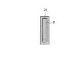
なお、外部断熱材40は、図3に示すように、ファイバーで編んだ布状の外装材22で内部材21を包んだ構造である。これは、外部断熱材40からの発塵によって基板100に異物が付着することなどを防止するためである。つまり、発塵性の高いカーボンフェルト、石英ファイバー、アルミナファイバーなどを内部材21とし、内部材21を発塵性の低い外装材22で覆うことにより、外部断熱材40からの発塵が抑制される。外装材22には、グラスファイバーやアルミナファイバーで編んで布状にしたものを採用可能である。ファイバーを編んで布状にすることにより、外装材22からの発塵が抑制される。 As shown in FIG. 3, the external
内部材21と外装材22の組み合わせは任意である。例えば、カーボンフェルトを内部材21に使用し、グラスファイバー布を外装材22に使用する。具体的には、厚みが9.5mm、密度が8〜10kg/m3、熱伝導率が0.2〜0.4W/m/K(K:1000〜2000℃)のカーボンフェルトと、厚みが0.18mm、耐熱温度が550℃、織り方が平織りのグラスファイバー布を組み合わせる。或いは、ブランケット状のアルミナファイバーを内部材21に使用し、アルミナファイバー布を外装材22に使用する。具体的には、厚みが12.5mm、密度が100〜160kg/m3、熱伝導率が0.07〜0.24W/m/K(K:400〜1000℃)、耐熱温度が1300℃のブランケット状のアルミナファイバーと、厚みが0.65mm、耐熱温度が1000℃、織り方が朱子織りのアルミナファイバー布を組み合わせる。または、内部材21にブランケット状の石英ファイバーを使用し、外装材22にアルミナファイバー布を使用してもよい。The combination of the
一般的に、カーボンフェルト、石英ファイバー、アルミナファイバーには、形状安定のために有機添加剤をコーティングすることが多い。しかし、減圧下の加熱によって有機添加剤がチャンバー20内で蒸発及び拡散して、チャンバー20の壁面や基板100を汚染するおそれがある。つまり、コンタミネーションによって製造された半導体装置の性能が劣化するおそれがある。加熱による有機添加剤の蒸発は避けられないため、外装材22及び内部材21は、有機添加剤を含有していない無機材料のみで構成されている。 In general, carbon felt, quartz fiber, and alumina fiber are often coated with an organic additive for shape stabilization. However, there is a possibility that the organic additive evaporates and diffuses in the
また、外部断熱材40の表面には、外部断熱材40内部の空洞に繋がる開口部が存在する。表面における開口率が小さいと、チャンバー20内を真空状態にする際に外部断熱材40の内部に溜まったガスの排出が容易に行えず、真空状態にするまでの所要時間が増大する。したがって、チャンバー20の真空排気が速やかに行えるように、外部断熱材40の表面の開口率は大きいことが好ましい。 In addition, on the surface of the external
外装材22で内部材21を覆う際、外装材22を縫い合わせる。ステンレス製の金属糸(ナスロン)を使用し、ミシンを使用した3mmピッチのかがり縫いで外装材22を縫い合わせた。外部断熱材40も高温に加熱されるため、高温耐性のある金属糸を使用する必要がある。外部断熱材40に有機添加材を使用していないため、縫い方もほつれにくいかがり縫い等が推奨される。 When covering the
基板ホルダ10に搭載された複数の基板すべての温度均一性を向上するために、チャンバー20の内壁を覆うように外部断熱材40が配置され、更に、外部断熱材40の表面に外部熱反射板50が配置されている。これにより、基板ホルダ10の中央部に配置された基板100と基板ホルダ10の外縁部でチャンバー20の壁面に近い位置に配置された基板100との間で基板温度の差が生じることを防止できる。更に、基板ホルダ10の底板12に近い部分と遠い部分との間で基板温度の差が生じることを防止できる。 In order to improve the temperature uniformity of all of the plurality of substrates mounted on the
なお、外部熱反射板50の温度上昇に熱エネルギーが消費されないように、外部熱反射板50の熱容量はできるだけ小さいことが好ましい。例えば、外部熱反射板50の厚みを薄くすることにより、熱容量を小さくする。ステンレスやアルミニウムなどの薄板材が外部熱反射板50に使用される。ステンレスの薄板材の厚みは0.2mm〜0.5mm程度である。 In addition, it is preferable that the heat capacity of the external
図1に示した半導体製造装置1によって基板100を加熱した実験では、基板加熱時の圧力が1パスカル以下、基板温度が450℃の加熱条件において、外部断熱材40からのガス放出量は36.8Pa・m/秒であった。なお、ガス放出量が100Pa・m/秒では問題なく基板100を加熱処理できることを確認した。また、加熱処理後の基板100上では、0.1mm2以上のサイズの目視可能なパーティクルが0個であった。In the experiment in which the
以上に説明したように、第1の実施形態係る半導体製造装置1では、外部断熱材40が加熱装置30の出力する熱を吸収することにより、チャンバー20への熱の伝達が抑制される。このため、大きな熱質量のあるチャンバー20の加熱に消費される熱エネルギーが不要になる。その結果、エネルギー効率良く基板100を加熱することができ、基板加熱処理における基板温度の昇温レートを向上できる。これにより、低パワーでの基板加熱が可能となると共に、基板100の加熱時間が短縮されて、1枚当たりの処理時間を短くできる。また、熱質量が減少するために、温度制御の精度が向上する。 As described above, in the semiconductor manufacturing apparatus 1 according to the first embodiment, the external
更に、チャンバー20壁面での熱エネルギーの放出が抑制されるため、チャンバー壁面付近での基板温度の低下を防止できる。これにより、基板100の温度均一性の劣化が生じない。また、チャンバー20の外側に取り付けられている部品の温度上昇が抑制されるため、それらの部品の熱劣化・損傷を防ぐことができる。 Furthermore, since the release of thermal energy on the wall surface of the
図1に示した半導体製造装置1は、例えばインライン式製造装置の一部として使用可能である。図4に、処理工程前に基板100を予備加熱するための加熱装置として半導体製造装置1を使用する例を示す。図4は、予備加熱装置である半導体製造装置1、処理装置2、取り出し室3からなるインライン式製造装置である。処理装置2は、例えば成膜装置、エッチング装置、スパッタ装置などである。 The semiconductor manufacturing apparatus 1 shown in FIG. 1 can be used as a part of an inline manufacturing apparatus, for example. FIG. 4 shows an example in which the semiconductor manufacturing apparatus 1 is used as a heating apparatus for preheating the
図4に示したインライン式製造装置では、基板100を搭載した基板ホルダ10が半導体製造装置1に搬入されて、所定の温度まで基板100が加熱される。所定の温度に達した基板100を搭載した基板ホルダ10は処理装置2に搬入され、基板100の成膜処理などが行われる。処理後、処理装置2から取り出し室3に搬送された基板ホルダ10が、取り出し室3から取り出される。 In the in-line manufacturing apparatus shown in FIG. 4, the
なお、インライン式製造装置が、取り出し室3を備えない、予備加熱装置である半導体製造装置1と処理装置2からなる構造であってもよい。 The in-line manufacturing apparatus may have a structure including the semiconductor manufacturing apparatus 1 and the
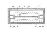
(第2の実施形態)
基板100を搭載した基板ホルダ10は、搬送装置によってチャンバー20に搬入され、且つチャンバー20から搬出されることが多い。このため、図5に示すように、基板ホルダ10と加熱装置30以外に、基板ホルダ10を搬送する基板ホルダ搬送装置60や加熱装置30に電力を供給する電力供給機構70がチャンバー20内に配置されている。加熱装置30によって加熱された場合、基板ホルダ搬送装置60や電力供給機構70が損傷したり劣化したりすることがある。また、基板100の昇温に寄与せずに、熱エネルギーが無駄に消費されることになる。(Second Embodiment)
In many cases, the
このため、図5に示すように、チャンバー20内に、基板ホルダ10及び加熱装置30を囲む内部断熱機構200を配置することが有効である。基板ホルダ搬送装置60や電力供給機構70は、内部断熱機構200とチャンバー20壁面との間に配置される。 Therefore, as shown in FIG. 5, it is effective to arrange an internal
内部断熱機構200の内壁、即ち基板ホルダ10や加熱装置30に対向する面は内部断熱材240により覆われ、内部断熱材240の表面には内部熱反射板250が配置されている。内部断熱材240には、外部断熱材40と同様の材料を使用可能である。即ち、内部断熱材240は、グラスファイバーやアルミナファイバーで編んだ布状の外装材22によって、カーボンフェルト、石英ファイバー、アルミナファイバーなどの内部材21を包んだ構造の無機材料からなる。 The inner wall of the internal
また、基板ホルダ10や加熱装置30に対向する内部熱反射板250には、外部熱反射板50と同様の材料を使用可能である。即ち、熱容量の小さいステンレスやアルミニウムの薄板材が内部熱反射板250に使用される。 In addition, the same material as that of the external
図5に示した第2の実施形態に係る半導体製造装置1によれば、チャンバー20内の基板ホルダ10以外の構成物への熱エネルギーの伝達が抑制され、効率よく基板ホルダ10を加熱することができる。その結果、基板加熱処理における基板温度の昇温レートを向上できる。また、加熱処理による基板ホルダ搬送装置60や電力供給機構70の損傷や劣化を防止できる。 According to the semiconductor manufacturing apparatus 1 according to the second embodiment shown in FIG. 5, the transfer of thermal energy to components other than the
なお、図5に示した半導体製造装置1でも、図1と同様に、チャンバー20の内壁は外部断熱材40で覆われ、外部断熱材40の表面に外部熱反射板50が配置されている。このため、内部断熱機構200の外側に放出された熱エネルギーによるチャンバー20の温度上昇が抑制されるなど、熱エネルギーの無駄な消費を抑えることができる。更に、チャンバー20の外側に取り付けられている部品の熱劣化・損傷を防ぐことができる。 In the semiconductor manufacturing apparatus 1 shown in FIG. 5 as well, the inner wall of the
(第3の実施形態)
本発明の第3の実施形態に係る半導体製造装置1は、図6に示すように、基板100が搭載された基板ホルダ10の下部に接して加熱装置30が配置されている。図6に示した加熱装置30は例えばシースヒータであり、基板ホルダ10を介して基板100に熱を伝達させることにより、基板100を所定の基板温度に設定する。その他の点については、図1に示した第1の実施形態と同様である。即ち、チャンバー20の内壁は外部断熱材40で覆われ、外部断熱材40の表面に外部熱反射板50が配置されている。(Third embodiment)
In the semiconductor manufacturing apparatus 1 according to the third embodiment of the present invention, as shown in FIG. 6, a
チャンバー20の内壁に外部断熱材40を配置しない場合には、60秒間加熱したときの基板100の温度は375℃であった。これに対し、チャンバー20の内壁に外部断熱材40及び外部熱反射板50を配置した場合には、60秒間の加熱により基板100の温度は475℃であり、基板100の昇温レートの向上、及び到達温度の上昇が確認された。 When the external
図6に示した半導体製造装置1では、図1に示した加熱装置30を使用する場合と異なり、基板ホルダ10に搭載された基板100の周囲に加熱装置30が配置されていない。このため、基板100の成膜処理やエッチング処理、スパッタ処理などをチャンバー20内で行うことが可能である。 In the semiconductor manufacturing apparatus 1 shown in FIG. 6, unlike the case where the
つまり、図6に示した半導体製造装置1では、基板100の予備加熱工程と、予備加熱工程後の処理工程を連続して1つの製造装置で行うことができる。例えば、基板ホルダ10をアノード電極として使用することで、半導体製造装置1をプラズマ成膜装置として使用可能である。 That is, in the semiconductor manufacturing apparatus 1 shown in FIG. 6, the preheating process of the
図7に、図6に示した半導体製造装置1をプラズマCVD成膜装置として使用する構成例を示す。図7に示したプラズマCVD成膜装置による成膜処理の例を以下に説明する。 FIG. 7 shows a configuration example in which the semiconductor manufacturing apparatus 1 shown in FIG. 6 is used as a plasma CVD film forming apparatus. An example of a film forming process by the plasma CVD film forming apparatus shown in FIG. 7 will be described below.
基板100の加熱処理の終了後に、チャンバー20内のガスを排気して、チャンバー20内を高真空にする。その後、基板100に形成する薄膜の原料ガスがチャンバー20内に導入され、チャンバー20内が所定のガス圧に調整される。次いで、交流電源300によって所定の交流電力が基板ホルダ10と高周波電極310間に供給される。これにより、チャンバー20内の原料ガスがプラズマ化される。形成されたプラズマに基板100を曝すことによってプラズマ中の励起種を基板100の表面で反応させ、基板100の表面に薄膜が形成される。その後、原料ガスを排気してチャンバー20内を高真空にする。以上により、基板100上に薄膜が形成される。 After the heat treatment of the
例えば、図7に示した半導体製造装置1によって太陽電池の反射防止膜やパッシベーション膜を形成できる。例えば、太陽電池の反射防止膜を形成する場合には、屈折率が1.9〜2.3、膜厚が70〜100nm程度の窒化シリコン(SiN)膜などを基板100上に形成する。成膜時の基板温度は300℃以上である。なお、加熱装置30を、処理工程中の基板100の温度を設定するために使用できる。 For example, an antireflection film or a passivation film for a solar cell can be formed by the semiconductor manufacturing apparatus 1 shown in FIG. For example, in the case of forming an antireflection film for a solar cell, a silicon nitride (SiN) film having a refractive index of 1.9 to 2.3 and a film thickness of about 70 to 100 nm is formed on the
他は、第1の実施形態と実質的に同様であり、重複した記載を省略する。 Others are substantially the same as those in the first embodiment, and redundant description is omitted.
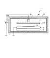
(第4の実施形態)
上記では、基板ホルダ10がボートタイプである場合を例示的に説明したが、基板ホルダ10が、水平方向に延伸する搭載面に基板100が搭載されるカートタイプの基板ホルダの場合にも本発明は適用可能である。図8に、基板ホルダ10にカートタイプを使用した第4の実施形態に係る半導体製造装置1を示す。図8に示す半導体製造装置1では、基板ホルダ10に複数の基板100を水平に並べた状態で、基板ホルダ10の上下に配置した加熱装置30により基板100を加熱する。加熱装置30には、ランプヒータなどを採用可能である。(Fourth embodiment)
In the above description, the case where the
図8に示すように、チャンバー20内に配置された基板ホルダ搬送装置60の周囲に、内部断熱材240が配置されている。内部断熱材240には、外部断熱材40と同様の材料を使用可能である。即ち、内部断熱材240は、グラスファイバーやアルミナファイバーで編んだ布状の外装材22によって、カーボンフェルト、石英ファイバー、アルミナファイバーなどの内部材21を包んだ構造の無機材料からなる。 As shown in FIG. 8, an internal
内部断熱材240の表面に内部熱反射板を配置してもよく、この内部熱反射板に外部熱反射板50と同様の材料を使用可能である。即ち、熱容量の小さいステンレスやアルミニウムの薄板材が内部熱反射板に使用される。 An internal heat reflecting plate may be disposed on the surface of the internal
図8に示した第4の実施形態に係る半導体製造装置1によれば、カートタイプの基板ホルダ10を使用した場合に、チャンバー20内の基板ホルダ10以外の構成物への熱エネルギーの伝達が抑制され、高いエネルギー効率で基板ホルダ10を加熱することができると共に、チャンバー20内の構成物の損傷や劣化を防止できる。他は、既に説明した実施形態と実質的に同様であり、重複した記載を省略する。 According to the semiconductor manufacturing apparatus 1 according to the fourth embodiment shown in FIG. 8, when a cart-
(第5の実施形態)
図6、図7に、ボートタイプの基板ホルダ10の下部に接して加熱装置30が配置されている例を示した。図9に示すように、基板ホルダ10がカートタイプの基板ホルダの場合にも、基板ホルダ10の下部に接して加熱装置30を配置し、基板ホルダ10を介して基板100に熱を伝達させることにより、基板100を所定の基板温度に設定することができる。その他の点については図7に示した第3の実施形態と同様であり、図9に示した第5の実施形態に係る半導体製造装置1のチャンバー20の内壁は外部断熱材40で覆われ、外部断熱材40の表面に外部熱反射板50が配置されている。図9に示した加熱装置30は例えばシースヒータである。(Fifth embodiment)
FIGS. 6 and 7 show examples in which the
図9に示した半導体製造装置1では、基板ホルダ10に搭載された基板100の周囲に加熱装置30が配置されていないため、基板100の成膜処理やエッチング処理、スパッタ処理などをチャンバー20内で行うことが可能である。つまり、基板100の予備加熱工程と、予備加熱工程後の処理工程を連続して1つの製造装置で行うことができる。 In the semiconductor manufacturing apparatus 1 shown in FIG. 9, since the
図9は、基板ホルダ10をアノード電極として使用することで、半導体製造装置1をプラズマCVD成膜装置として構成した例を示している。つまり、図7を参照して説明した方法と同様にして、基板100上に薄膜が形成される。即ち、基板100の加熱処理の終了後に基板100に形成する薄膜の原料ガスがチャンバー20内に導入される。そして、交流電源300によって所定の交流電力を基板ホルダ10と高周波電極310間に供給して、チャンバー20内の原料ガスをプラズマ化する。形成されたプラズマに基板100を曝すことによってプラズマ中の励起種を基板100の表面で反応させ、基板100の表面に薄膜が形成される。 FIG. 9 shows an example in which the semiconductor manufacturing apparatus 1 is configured as a plasma CVD film forming apparatus by using the
以上に説明したように、第5の実施形態に係る半導体製造装置1によれば、カートタイプの基板ホルダ10に複数の基板100を水平に並べた状態で、基板ホルダ10直下に配置した加熱装置30により基板100が高いエネルギー効率で加熱される。また、チャンバー20の外側に取り付けられている部品の温度上昇が抑制されるため、それらの部品の熱劣化・損傷を防ぐことができる。更に、加熱処理後の基板100を対象とする処理工程を半導体製造装置1により実施できる。他は、既に説明した実施形態と実質的に同様であり、重複した記載を省略する。 As described above, according to the semiconductor manufacturing apparatus 1 according to the fifth embodiment, the heating apparatus that is arranged directly below the
(第6の実施形態)
図9に示した半導体製造装置1が複数の基板100を同時に処理する半導体製造装置であるのに対して、図10に示した第6の実施形態に係る半導体製造装置1は、基板100を1枚ずつ処理する枚葉式の半導体製造装置である。その他の点については図9に示した第5の実施形態と同様であり、チャンバー20の内壁は外部断熱材40で覆われ、外部断熱材40の表面に外部熱反射板50が配置されている。図10に示した加熱装置30は例えばシースヒータである。(Sixth embodiment)
The semiconductor manufacturing apparatus 1 shown in FIG. 9 is a semiconductor manufacturing apparatus that processes a plurality of
図10に示した半導体製造装置1においても、基板ホルダ10に搭載された基板100の周囲に加熱装置30が配置されていないため、基板100の成膜処理やエッチング処理、スパッタ処理などをチャンバー20内で行うことが可能である。つまり、基板100の予備加熱工程と、予備加熱工程後の処理工程を連続して1つの製造装置で行うことができる。 Also in the semiconductor manufacturing apparatus 1 shown in FIG. 10, since the
したがって、例えば図10に示すように基板ホルダ10をプラズマCVD成膜装置のアノード電極として使用することにより、基板100上に薄膜が形成される。即ち、基板100の加熱処理の終了後に、交流電源300によって所定の交流電力を基板ホルダ10と高周波電極310間に供給して、チャンバー20内に導入された原料ガスをプラズマ化する。形成されたプラズマに基板100を曝すことによって、基板100の表面に薄膜が形成される。 Therefore, for example, as shown in FIG. 10, a thin film is formed on the
以上に説明したように、第6の実施形態に係る半導体製造装置1によれば、基板ホルダ10直下に配置した加熱装置30によって、カートタイプの基板ホルダ10に水平に搭載された1枚の基板100が基板ホルダ10を介して高いエネルギー効率で加熱される。また、チャンバー20の外側に取り付けられている部品の温度上昇が抑制されるため、それらの部品の熱劣化・損傷を防ぐことができる。更に、加熱処理後の基板100を対象とする処理工程を半導体製造装置1により実施できる。他は、既に説明した実施形態と実質的に同様であり、重複した記載を省略する。 As described above, according to the semiconductor manufacturing apparatus 1 according to the sixth embodiment, one substrate mounted horizontally on the cart-
(その他の実施形態)
上記のように、本発明は第1乃至第6の実施形態によって記載したが、この開示の一部をなす論述及び図面はこの発明を限定するものであると理解すべきではない。この開示から当業者には様々な代替実施形態、実施例及び運用技術が明らかとなろう。(Other embodiments)
As described above, the present invention has been described according to the first to sixth embodiments. However, it should not be understood that the description and drawings constituting a part of this disclosure limit the present invention. From this disclosure, various alternative embodiments, examples and operational techniques will be apparent to those skilled in the art.
例えば、第1乃至第3の実施形態の説明においてはチャンバー20が円筒形状である場合について説明した。しかし、チャンバー20が円筒形状以外の、例えば直方体形状であってもよい。 For example, in the description of the first to third embodiments, the case where the
このように、本発明はここでは記載していない様々な実施形態等を含むことは勿論である。したがって、本発明の技術的範囲は上記の説明から妥当な請求の範囲に係る発明特定事項によってのみ定められるものである。 As described above, the present invention naturally includes various embodiments not described herein. Therefore, the technical scope of the present invention is defined only by the invention specifying matters according to the scope of claims reasonable from the above description.
本発明の半導体製造装置は、基板を加熱処理する工程を含む半導体製造に利用可能である。 The semiconductor manufacturing apparatus of the present invention can be used for semiconductor manufacturing including a step of heat-treating a substrate.
Claims (5)
Translated fromJapanese前記チャンバーの内部に配置され、前記基板ホルダに搭載された前記基板を加熱する加熱装置と、
ファイバーで編んだ布状の外装材で内部材を包んだ構造の有機添加剤を含有していない無機材料からなり、前記チャンバーの内壁を覆って配置された外部断熱材と、
前記外部断熱材の前記加熱装置に対向する表面上に配置された外部熱反射板と、
前記基板ホルダ及び前記加熱装置を囲んで前記チャンバー内に配置された内部断熱機構と
を備え、
ファイバーで編んだ布状の外装材で内部材を包んだ構造の有機添加剤を含有していない無機材料からなる内部断熱材が前記内部断熱機構の内壁を覆って配置され、且つ、内部熱反射板が前記内部断熱材の前記加熱装置に対向する表面上に配置されていることを特徴とする半導体製造装置。A chamber for storing a substrate holder on which a substrate is mounted;
A heating device that is disposed inside the chamber and that heats the substrate mounted on the substrate holder;
An external heat insulating material that is made of an inorganic material that does not contain an organic additive having a structure in which an inner member is wrapped with a cloth-like exterior material knitted with fiber, and is arranged so as to cover the inner wall of the chamber;
An external heat reflector disposed on the surface of the external heat insulating material facing the heating device;
An internal heat insulating mechanism disposed in the chamber surrounding the substrate holder and the heating device ,
An internal heat insulating material made of an inorganic material not containing an organic additive having a structure in which an inner member is wrapped with a cloth-like outer material knitted with fiber is arranged to cover the inner wall of the internal heat insulating mechanism, and the internal heat reflection The board | substrate is arrange | positioned on the surface facing the said heating apparatus of the said internal heat insulating material, The semiconductor manufacturing apparatus characterizedby the above-mentioned .
前記加熱装置が前記基板取り付け板間に配置された複数のランプヒータであることを特徴とする請求項1に記載の半導体製造装置。The substrate holder is a boat type having a plurality of substrate mounting plates that are respectively defined as main surfaces on which a mounting surface on which the substrate is mounted extends in the vertical direction and are spaced apart from each other in parallel.
The semiconductor manufacturing apparatus according to claim 1, wherein the heating device is a plurality of lamp heaters disposed between the substrate mounting plates.
前記加熱装置が前記基板ホルダの上下に配置されたランプヒータであることを特徴とする請求項1に記載の半導体製造装置。The substrate holder is a cart type that horizontally mounts the substrate on a mounting surface that extends in a horizontal direction,
The semiconductor manufacturing apparatus according to claim 1, wherein the heating device is a lamp heater disposed above and below the substrate holder.
Applications Claiming Priority (1)
| Application Number | Priority Date | Filing Date | Title |
|---|---|---|---|
| PCT/JP2012/062992WO2013175562A1 (en) | 2012-05-22 | 2012-05-22 | Semiconductor manufacturing apparatus |
Publications (2)
| Publication Number | Publication Date |
|---|---|
| JPWO2013175562A1 JPWO2013175562A1 (en) | 2016-01-12 |
| JP5900614B2true JP5900614B2 (en) | 2016-04-06 |
Family
ID=49623295
Family Applications (1)
| Application Number | Title | Priority Date | Filing Date |
|---|---|---|---|
| JP2014516546AExpired - Fee RelatedJP5900614B2 (en) | 2012-05-22 | 2012-05-22 | Semiconductor manufacturing equipment |
Country Status (2)
| Country | Link |
|---|---|
| JP (1) | JP5900614B2 (en) |
| WO (1) | WO2013175562A1 (en) |
Families Citing this family (3)
| Publication number | Priority date | Publication date | Assignee | Title |
|---|---|---|---|---|
| JP6680939B1 (en)* | 2019-09-27 | 2020-04-15 | 信越石英株式会社 | Structure including glass cloth light reflector |
| CN211848134U (en)* | 2020-01-14 | 2020-11-03 | 宁夏隆基乐叶科技有限公司 | A heating device and coating equipment |
| CN114727467B (en)* | 2022-04-13 | 2023-06-16 | 中国科学技术大学 | Combined direct-heating lanthanum hexaboride plasma source |
Family Cites Families (7)
| Publication number | Priority date | Publication date | Assignee | Title |
|---|---|---|---|---|
| JPS63161611A (en)* | 1986-12-25 | 1988-07-05 | Toshiba Ceramics Co Ltd | Vertical type furnace |
| JP2651601B2 (en)* | 1987-07-31 | 1997-09-10 | 東京エレクトロン株式会社 | heating furnace |
| JPH04335520A (en)* | 1991-05-13 | 1992-11-24 | Fuji Electric Co Ltd | Vapor phase growth equipment |
| JPH05164472A (en)* | 1991-12-13 | 1993-06-29 | Asahi Glass Co Ltd | Expandable fibrous insulation and airtight insulation |
| JPH05164473A (en)* | 1991-12-18 | 1993-06-29 | Asahi Glass Co Ltd | Basic unit block aggregate heat insulation material and heat insulation method for semiconductor heat treatment furnace |
| JP3125280B2 (en)* | 1992-11-10 | 2001-01-15 | 日立電子エンジニアリング株式会社 | Cleaning method for CVD equipment |
| JP4089113B2 (en)* | 1999-12-28 | 2008-05-28 | 株式会社Ihi | Thin film production equipment |
- 2012
- 2012-05-22WOPCT/JP2012/062992patent/WO2013175562A1/enactiveApplication Filing
- 2012-05-22JPJP2014516546Apatent/JP5900614B2/ennot_activeExpired - Fee Related
Also Published As
| Publication number | Publication date |
|---|---|
| JPWO2013175562A1 (en) | 2016-01-12 |
| WO2013175562A1 (en) | 2013-11-28 |
Similar Documents
| Publication | Publication Date | Title |
|---|---|---|
| US8336489B2 (en) | Thermal evaporation apparatus, use and method of depositing a material | |
| TWI554641B (en) | A substrate processing apparatus, a manufacturing method of a semiconductor device, and a recording medium | |
| US8366831B2 (en) | Evaporation source | |
| US20080092821A1 (en) | Quartz Jig and Semiconductor Manufacturing Apparatus | |
| JP2013211138A (en) | Evaporation source and vacuum deposition device using the same | |
| JP2007251126A (en) | Semiconductor batch heating assembly | |
| JP5900614B2 (en) | Semiconductor manufacturing equipment | |
| JP2011077502A (en) | Thermal treatment apparatus | |
| KR20170117198A (en) | Heating arrangement and method for heating substrates | |
| JP6011191B2 (en) | Semiconductor manufacturing equipment | |
| CN108411362B (en) | Chamber and epitaxial growth equipment | |
| JP7049818B2 (en) | Film forming equipment | |
| KR101104060B1 (en) | Vertical boat for processing solar substrate and process tube having same | |
| KR101354600B1 (en) | Improved boat, and heat treatment chamber and apparatus of substrate having the same | |
| JP2011029597A (en) | Method of manufacturing semiconductor device, method of manufacturing substrate, and substrate treatment apparatus | |
| JP2004059992A (en) | Organic thin film deposition apparatus | |
| TWI540662B (en) | Substrate processing apparatus and substrate processing system | |
| JP2005072468A (en) | Heat treatment apparatus of semiconductor wafer | |
| KR101420712B1 (en) | Improved Chamber for Heat Treatment of Substrates and Heat Treatment Apparatus of Substrate Having the Same | |
| JP6065110B2 (en) | Substrate processing system | |
| KR101431564B1 (en) | Improved Chamber for Heat Treatment of Substrates and Heat Treatment Apparatus of Substrate Having the Same | |
| KR101593493B1 (en) | Themal processing apparatus of large area glass substrate | |
| KR20080046968A (en) | Substrate holding device and thin film lamination device including same | |
| KR101189398B1 (en) | Deposition apparatus | |
| KR101539758B1 (en) | Chamber for Heat Treatment of Mutiple Substrates and Heat Treatment Apparatus of Substrate Having the Same |
Legal Events
| Date | Code | Title | Description |
|---|---|---|---|
| TRDD | Decision of grant or rejection written | ||
| A01 | Written decision to grant a patent or to grant a registration (utility model) | Free format text:JAPANESE INTERMEDIATE CODE: A01 Effective date:20160209 | |
| A61 | First payment of annual fees (during grant procedure) | Free format text:JAPANESE INTERMEDIATE CODE: A61 Effective date:20160222 | |
| R151 | Written notification of patent or utility model registration | Ref document number:5900614 Country of ref document:JP Free format text:JAPANESE INTERMEDIATE CODE: R151 | |
| LAPS | Cancellation because of no payment of annual fees |