JP5899565B2 - Capacitor with switch and circuit including capacitor with switch - Google Patents
Capacitor with switch and circuit including capacitor with switchDownload PDFInfo
- Publication number
- JP5899565B2 JP5899565B2JP2013196295AJP2013196295AJP5899565B2JP 5899565 B2JP5899565 B2JP 5899565B2JP 2013196295 AJP2013196295 AJP 2013196295AJP 2013196295 AJP2013196295 AJP 2013196295AJP 5899565 B2JP5899565 B2JP 5899565B2
- Authority
- JP
- Japan
- Prior art keywords
- switch
- capacitor
- control circuit
- circuit
- mos transistor
- Prior art date
- Legal status (The legal status is an assumption and is not a legal conclusion. Google has not performed a legal analysis and makes no representation as to the accuracy of the status listed.)
- Active
Links
Images


Classifications
- H—ELECTRICITY
- H03—ELECTRONIC CIRCUITRY
- H03M—CODING; DECODING; CODE CONVERSION IN GENERAL
- H03M1/00—Analogue/digital conversion; Digital/analogue conversion
- H03M1/66—Digital/analogue converters
- H—ELECTRICITY
- H01—ELECTRIC ELEMENTS
- H01L—SEMICONDUCTOR DEVICES NOT COVERED BY CLASS H10
- H01L23/00—Details of semiconductor or other solid state devices
- H01L23/48—Arrangements for conducting electric current to or from the solid state body in operation, e.g. leads, terminal arrangements ; Selection of materials therefor
- H01L23/482—Arrangements for conducting electric current to or from the solid state body in operation, e.g. leads, terminal arrangements ; Selection of materials therefor consisting of lead-in layers inseparably applied to the semiconductor body (electrodes)
- H01L23/4824—Pads with extended contours, e.g. grid structure, branch structure, finger structure
- H—ELECTRICITY
- H01—ELECTRIC ELEMENTS
- H01L—SEMICONDUCTOR DEVICES NOT COVERED BY CLASS H10
- H01L23/00—Details of semiconductor or other solid state devices
- H01L23/52—Arrangements for conducting electric current within the device in operation from one component to another, i.e. interconnections, e.g. wires, lead frames
- H01L23/522—Arrangements for conducting electric current within the device in operation from one component to another, i.e. interconnections, e.g. wires, lead frames including external interconnections consisting of a multilayer structure of conductive and insulating layers inseparably formed on the semiconductor body
- H01L23/5222—Capacitive arrangements or effects of, or between wiring layers
- H01L23/5223—Capacitor integral with wiring layers
- H—ELECTRICITY
- H01—ELECTRIC ELEMENTS
- H01L—SEMICONDUCTOR DEVICES NOT COVERED BY CLASS H10
- H01L23/00—Details of semiconductor or other solid state devices
- H01L23/52—Arrangements for conducting electric current within the device in operation from one component to another, i.e. interconnections, e.g. wires, lead frames
- H01L23/535—Arrangements for conducting electric current within the device in operation from one component to another, i.e. interconnections, e.g. wires, lead frames including internal interconnections, e.g. cross-under constructions
- H—ELECTRICITY
- H03—ELECTRONIC CIRCUITRY
- H03M—CODING; DECODING; CODE CONVERSION IN GENERAL
- H03M1/00—Analogue/digital conversion; Digital/analogue conversion
- H03M1/12—Analogue/digital converters
- H—ELECTRICITY
- H10—SEMICONDUCTOR DEVICES; ELECTRIC SOLID-STATE DEVICES NOT OTHERWISE PROVIDED FOR
- H10D—INORGANIC ELECTRIC SEMICONDUCTOR DEVICES
- H10D84/00—Integrated devices formed in or on semiconductor substrates that comprise only semiconducting layers, e.g. on Si wafers or on GaAs-on-Si wafers
- H10D84/201—Integrated devices formed in or on semiconductor substrates that comprise only semiconducting layers, e.g. on Si wafers or on GaAs-on-Si wafers characterised by the integration of only components covered by H10D1/00 or H10D8/00, e.g. RLC circuits
- H10D84/204—Integrated devices formed in or on semiconductor substrates that comprise only semiconducting layers, e.g. on Si wafers or on GaAs-on-Si wafers characterised by the integration of only components covered by H10D1/00 or H10D8/00, e.g. RLC circuits of combinations of diodes or capacitors or resistors
- H10D84/212—Integrated devices formed in or on semiconductor substrates that comprise only semiconducting layers, e.g. on Si wafers or on GaAs-on-Si wafers characterised by the integration of only components covered by H10D1/00 or H10D8/00, e.g. RLC circuits of combinations of diodes or capacitors or resistors of only capacitors
- H10D84/217—Integrated devices formed in or on semiconductor substrates that comprise only semiconducting layers, e.g. on Si wafers or on GaAs-on-Si wafers characterised by the integration of only components covered by H10D1/00 or H10D8/00, e.g. RLC circuits of combinations of diodes or capacitors or resistors of only capacitors of only conductor-insulator-semiconductor capacitors
- H—ELECTRICITY
- H10—SEMICONDUCTOR DEVICES; ELECTRIC SOLID-STATE DEVICES NOT OTHERWISE PROVIDED FOR
- H10D—INORGANIC ELECTRIC SEMICONDUCTOR DEVICES
- H10D84/00—Integrated devices formed in or on semiconductor substrates that comprise only semiconducting layers, e.g. on Si wafers or on GaAs-on-Si wafers
- H10D84/80—Integrated devices formed in or on semiconductor substrates that comprise only semiconducting layers, e.g. on Si wafers or on GaAs-on-Si wafers characterised by the integration of at least one component covered by groups H10D12/00 or H10D30/00, e.g. integration of IGFETs
- H10D84/811—Combinations of field-effect devices and one or more diodes, capacitors or resistors
- H—ELECTRICITY
- H10—SEMICONDUCTOR DEVICES; ELECTRIC SOLID-STATE DEVICES NOT OTHERWISE PROVIDED FOR
- H10D—INORGANIC ELECTRIC SEMICONDUCTOR DEVICES
- H10D89/00—Aspects of integrated devices not covered by groups H10D84/00 - H10D88/00
- H10D89/10—Integrated device layouts
- H—ELECTRICITY
- H01—ELECTRIC ELEMENTS
- H01L—SEMICONDUCTOR DEVICES NOT COVERED BY CLASS H10
- H01L2924/00—Indexing scheme for arrangements or methods for connecting or disconnecting semiconductor or solid-state bodies as covered by H01L24/00
- H01L2924/0001—Technical content checked by a classifier
- H01L2924/0002—Not covered by any one of groups H01L24/00, H01L24/00 and H01L2224/00
Landscapes
- Engineering & Computer Science (AREA)
- Power Engineering (AREA)
- Physics & Mathematics (AREA)
- Condensed Matter Physics & Semiconductors (AREA)
- General Physics & Mathematics (AREA)
- Computer Hardware Design (AREA)
- Microelectronics & Electronic Packaging (AREA)
- Theoretical Computer Science (AREA)
- Semiconductor Integrated Circuits (AREA)
- Metal-Oxide And Bipolar Metal-Oxide Semiconductor Integrated Circuits (AREA)
Description
Translated fromJapanese本発明はICやLSI内の容量をスイッチで切替える回路に関する。The present invention relates to a circuit for switching a capacitor in an IC or LSI with a switch.
従来からICやLSI内部で容量をスイッチで切替える回路は、アナログ・フィルタ、ADコンバータ、発振器等に広く使われている。従来は配線層間膜を使った容量(以下「MIM容量」と言う)等とMOSスイッチをそれぞれ半導体基板上に形成し、配線で接続しているのが一般的である。一方、近年半導体プロセスがディープ・サブミクロン(0.1um程度以下)と呼ばれる時代になり、配線層間膜の厚みよりも配線間隔の方が狭くなってきた。このため配線を使った容量として、従来のMIM容量よりも、配線間を使った容量(以下「MOM容量」と言う)の方が面積効率が高くなりつつある。Conventionally, a circuit that switches a capacitor with a switch in an IC or LSI has been widely used for an analog filter, an AD converter, an oscillator, and the like. Conventionally, a capacitor using a wiring interlayer film (hereinafter referred to as “MIM capacitor”) and a MOS switch are generally formed on a semiconductor substrate and connected by wiring. On the other hand, in recent years, semiconductor processes have entered an era called deep sub-micron (about 0.1 μm or less), and the wiring interval has become narrower than the thickness of the wiring interlayer film. For this reason, as the capacity using the wiring, the capacity using the space between the wirings (hereinafter referred to as “MOM capacity”) is becoming more efficient than the conventional MIM capacity.
従来は、容量とスイッチをそれぞれ所定の大きさで作り、それを配線で結びつけていたため、各素子の分離領域含めると1um台〜10um台と大きなサイズだったのみならず、配線の浮遊容量が精度や特性を劣化させていた。また浮遊容量のため実質的にスイッチで切替えられる最小容量(分解能)は100fF程度がやっとだった。
本願は、MOM容量を用い、かつ容量とスイッチを以下に示す工夫をすることで、浮遊容量をほぼ1〜2桁減らし、小型化、高性能化、分解能向上を実現するものである。In the past, capacitors and switches were each made to a predetermined size and connected by wiring, so when including the isolation region of each element, it was not only a large size of 1 um to 10 um, but also the floating capacitance of the wiring was accurate And the characteristics deteriorated. In addition, because of the stray capacitance, the minimum capacitance (resolution) that can be switched by a switch is about 100 fF.
In the present application, the MOM capacitor is used, and the capacity and switch are devised as follows, thereby reducing the stray capacitance by approximately one to two digits, thereby realizing miniaturization, higher performance, and improved resolution.
図1は従来のスイッチ付容量の回路図の一例であり、本願の対象でもある。
容量C1〜C4がスイッチS1〜S4を介してつながっている。例えばC1が0.1pF、C2が0.2pF、C3が0.4pF、C4が0.8pFとすれば、スイッチS1〜S4の選択により0pF〜1.5pFの容量値を0.1pFステップで設定できる。なおスイッチはMOSトランジスタで作るのが一般的である。
実際にはこの回路が、フィルタやADコンバータや発振回路の容量の一部を構成している。スイッチはNチャネルMOSとPチャネルMOSトランジスタを並列につなぐ場合もある。FIG. 1 is an example of a circuit diagram of a conventional switched capacitor and is also the subject of the present application.
Capacitors C1 to C4 are connected via switches S1 to S4. For example, if C1 is 0.1 pF, C2 is 0.2 pF, C3 is 0.4 pF, and C4 is 0.8 pF, the capacitance value of 0 pF to 1.5 pF can be set in 0.1 pF steps by selecting the switches S1 to S4. The switch is generally made of a MOS transistor.
Actually, this circuit constitutes a part of the capacitance of the filter, AD converter, and oscillation circuit. The switch may connect an N channel MOS transistor and a P channel MOS transistor in parallel.
図2aは、図1の回路を従来の方法で半導体基板上に配置し、配線した平面図の一例である。C1〜C4は従来から用いられているMIM容量であり、C1が0.1pF、C2が0.2pF、C3が0.4pF、C4が0.8pFである。それぞれの一端はT1端子に接続され、他端はそれぞれスイッチS1〜S4を構成するMOSトランジスタに接続されている。各スイッチの他端は端子T2に接続されている。小さな四角はコンタクト・ホールをあらわしている。各スイッチの白抜きの細長い矩形は、MOSトランジスタのゲートを表し、ここには制御用のロジック信号が接続される(図示せず)。二点鎖線での断面図を図2bに示す。
容量用絶縁膜を挟んで容量の電極が存在する。FIG. 2a is an example of a plan view in which the circuit of FIG. 1 is arranged and wired on a semiconductor substrate by a conventional method. C1 to C4 are conventionally used MIM capacitors, where C1 is 0.1 pF, C2 is 0.2 pF, C3 is 0.4 pF, and C4 is 0.8 pF. One end of each is connected to the T1 terminal, and the other end is connected to the MOS transistors constituting the switches S1 to S4. The other end of each switch is connected to terminal T2. A small square represents a contact hole. The white, narrow rectangle of each switch represents the gate of a MOS transistor, to which a control logic signal is connected (not shown). A cross-sectional view taken along the two-dot chain line is shown in FIG. 2b.
A capacitor electrode exists with the capacitor insulating film interposed therebetween.
図3aは、図1の回路を従来の方法で半導体基板上に配置し、配線した平面図の別の一例である。C1〜C4はMOM容量であり、C1が0.1pF、C2が0.2pF、C3が0.4pF、C4が0.8pFとなるように各容量の電極の長辺方向(以下フィンガと言う)の数が選ばれている(図3aでは模式的に表しており、実際のフィンガ数とは異なる)。それぞれの一端はT1端子に接続され、他端はそれぞれスイッチS1〜S4を構成するMOSトランジスタに接続されている。各スイッチの他端は端子T2に接続されている。小さな四角はコンタクト・ホールをあらわしている。各スイッチの白抜きの細長い矩形は、MOSトランジスタのゲートを表し、ここには制御用のロジック信号が接続される(図示せず)。二点鎖線での断面図を図3bに示す。
容量用絶縁膜を挟んで容量の電極が存在する。FIG. 3a is another example of a plan view in which the circuit of FIG. 1 is arranged and wired on a semiconductor substrate by a conventional method. C1 to C4 are MOM capacitors, and the number of electrodes in the long side direction (hereinafter referred to as fingers) is selected so that C1 is 0.1 pF, C2 is 0.2 pF, C3 is 0.4 pF, and C4 is 0.8 pF. (It is schematically shown in FIG. 3a and is different from the actual number of fingers). One end of each is connected to the T1 terminal, and the other end is connected to the MOS transistors constituting the switches S1 to S4. The other end of each switch is connected to terminal T2. A small square represents a contact hole. The white, narrow rectangle of each switch represents the gate of a MOS transistor, to which a control logic signal is connected (not shown). A cross-sectional view taken along the two-dot chain line is shown in FIG. 3b.
A capacitor electrode exists with the capacitor insulating film interposed therebetween.
これら2例はともに、容量とスイッチをそれぞれ単独で作り、配線を施しているため、サイズが大きくなるのみならず、配線の浮遊容量が精度や特性を劣化させていた。また浮遊容量のため実質的にスイッチで切替えられる最小容量(分解能)は100fF程度がやっとだった。In both cases, the capacitance and the switch are individually made and wired, so that not only the size increases but also the floating capacitance of the wiring degrades the accuracy and characteristics. In addition, because of the stray capacitance, the minimum capacitance (resolution) that can be switched by a switch is about 100 fF.
本発明を適用すれば、配線の浮遊容量を最小にし、1fF以下の分解能で容量値を切り替えることが可能になり、さらに単調増加を保証することが可能になる等の利点がある。By applying the present invention, it is possible to minimize the stray capacitance of the wiring, to switch the capacitance value with a resolution of 1 fF or less, and to ensure a monotonous increase.
本発明は、容量とスイッチの方向とピッチ(繰り返しの間隔)を合わせることで、種々の利点を生むものである。
配線間隔を使ったMOM型容量素子と、スイッチとして動作するMOSトランジスタを接続している集積回路装置において、前記容量の電極間の方向と、前記MOSトランジスタのゲート間隔を同方向とし、これらを複数個近接して並べ、その繰り返しの間隔を等しくもしくは整数倍の関係とし、両者を短い配線で接続したことを特徴とするスイッチ付容量である。ここで特に重要なのは、サブミクロン・プロセスの場合、上記ピッチをほぼサブミクロンにできるということであり、従来に比べて1〜2桁小さく作れるということである。The present invention produces various advantages by matching the capacitance, the direction of the switch, and the pitch (repetition interval).
In an integrated circuit device in which a MOM type capacitive element using a wiring interval and a MOS transistor operating as a switch are connected, the direction between the electrodes of the capacitor and the gate interval of the MOS transistor are set in the same direction, The capacitors with switches are characterized in that they are arranged close to each other, their repetition intervals are made equal or an integral multiple, and both are connected by a short wiring. Particularly important here is that in the case of a sub-micron process, the pitch can be made substantially sub-micron, and it can be made 1 to 2 orders of magnitude smaller than the conventional one.
図4は本願の第一の実施例であり、MOM容量の2フィンガと、スイッチを構成するMOSトランジスタの2ゲートを同一ピッチ(繰り返し幅)となるように調整したものである。通常のLSIのレイアウト設計基準では、MOSトランジスタ側の最小ゲート・ピッチの方が、MOM容量の最小フィンガ・ピッチより狭いことが多いので、その場合はMOSトランジスタのゲート・ピッチを少し広げて、両者を一致させる必要がある。ただしそれに限定しない。
例えばMOM容量C11の2フィンガが、スイッチS11を構成するMOSトランジスタのドレインに接続され、かかるMOSトランジスタの2本のゲートは共通の制御信号に接続され(図示せず)、2つのソースは端子T2に接続されている。なお、右側のソースはスイッチS12の左側のソースと共用している。同様な構成でC25,S25まで繰り返されている。
このように隣のトランジスタとソースを共用することで、サブミクロン・オーダのピッチを実現でき、かつトランジスタの分離領域を不要なため、全体のトランジスタ占有面積を大幅に小さくすることができる。FIG. 4 shows a first embodiment of the present application, in which two fingers of an MOM capacitor and two gates of a MOS transistor constituting a switch are adjusted to have the same pitch (repetitive width). Under normal LSI layout design standards, the minimum gate pitch on the MOS transistor side is often narrower than the minimum finger pitch of the MOM capacitor. Need to match. However, it is not limited to this.
For example, two fingers of the MOM capacitor C11 are connected to the drains of the MOS transistors constituting the switch S11, the two gates of the MOS transistors are connected to a common control signal (not shown), and the two sources are connected to the terminal T2. It is connected to the. The right source is shared with the left source of the switch S12. The same configuration is repeated up to C25 and S25.
By sharing the source with the adjacent transistor in this way, a pitch of submicron order can be realized, and the isolation region of the transistor is unnecessary, so that the entire transistor occupation area can be greatly reduced.
スイッチS11の2本のゲートを制御することで0.1pFの容量をオン/オフできる。スイッチS12とスイッチS13の合計4本のゲートを制御することで0.2pFの容量をオン/オフできる。スイッチS14,S15,S16,S17の合計8本のゲートを制御することで0.4pFの容量をオン/オフできる。スイッチS18〜S25の合計16本のゲートを制御することで0.8pFの容量をオン/オフできる。これらの組合せで0〜1.5pFまで、0.1pFおきに任意の容量値を設定できる。The capacitance of 0.1 pF can be turned on / off by controlling the two gates of the switch S11. A 0.2 pF capacitance can be turned on / off by controlling a total of four gates of the switch S12 and the switch S13. A capacitance of 0.4 pF can be turned on / off by controlling a total of eight gates of the switches S14, S15, S16, and S17. By controlling a total of 16 gates of the switches S18 to S25, the capacitance of 0.8 pF can be turned on / off. With these combinations, an arbitrary capacitance value can be set from 0 to 1.5 pF every 0.1 pF.
他の制御方法としては、スイッチS18の2本のゲートを制御することで0.1pFの容量をオン/オフさせる。スイッチS14とスイッチS22の合計4本のゲートを制御することで0.2pFの容量をオン/オフさせる。スイッチS12,S16,S20,S24の合計8本のゲートを制御することで0.4pFの容量をオン/オフさせる。スイッチS11,S13,S15,S17,S19,S21,S23,S25の合計16本のゲートを制御することで0.8pFの容量をオン/オフさせる。これらの組合せでも0〜1.5pFまで、0.1pFおきに任意の容量値を設定できる。こうすると、仮にフィンガ間隔がチップの面内で傾斜を持つような場合でも、各容量値は平均化されるので、相対精度を向上することができる。As another control method, the capacitance of 0.1 pF is turned on / off by controlling the two gates of the switch S18. By controlling a total of four gates of the switch S14 and the switch S22, the capacitance of 0.2 pF is turned on / off. By controlling a total of eight gates of the switches S12, S16, S20, and S24, the 0.4 pF capacitance is turned on / off. By controlling a total of 16 gates of the switches S11, S13, S15, S17, S19, S21, S23, and S25, the capacitance of 0.8 pF is turned on / off. Even in these combinations, an arbitrary capacitance value can be set from 0 to 1.5 pF every 0.1 pF. In this way, even if the finger spacing has an inclination in the plane of the chip, the capacitance values are averaged, so that the relative accuracy can be improved.
さらに別の制御方法として、全てのスイッチをオフすると0pF、スイッチS11のみオンさせると0.1pF、スイッチS11とスイッチS12をオンさせると0.2pF、スイッチS11,S12,S13をオンさせると0.3pF、スイッチS11,S12,S13,S14をオンさせると0.4pF、・・・スイッチS11〜S25をオンさせると1.5pFが得られる。このような漸次オンする数を増やしていく制御方式を温度計型制御という。この方式では容量値が漸増するので、単調増加性が確実に保証される。これは帰還系で使う場合に好都合である。本実施例の部分はそのままで、それを制御するロジック部の工夫で温度計型制御も実現できるのが特徴である。As another control method, when all switches are turned off, 0 pF, when only switch S11 is turned on, 0.1 pF, when switches S11 and S12 are turned on, 0.2 pF, and when switches S11, S12, S13 are turned on, 0.3 pF, switch When S11, S12, S13, and S14 are turned on, 0.4 pF is obtained, and when switches S11 to S25 are turned on, 1.5 pF is obtained. Such a control method of gradually increasing the number of ON is called thermometer type control. In this method, since the capacitance value gradually increases, monotonic increase is surely ensured. This is convenient when used in a feedback system. The feature of this embodiment is that the thermometer type control can also be realized by devising the logic unit for controlling it without changing the part.
さらに別の制御方法として、全てのスイッチをオフすると0pF、スイッチS18のみオンさせると0.1pF、スイッチS18とスイッチS14をオンさせると0.2pF、スイッチS18,S14,S22をオンさせると0.3pF、スイッチS18,S14,S22,S12をオンさせると0.4pF、・・・スイッチS11〜S25をオンさせると1.5pFが得られる。このように出来るだけ1箇所付近に集中しないように制御すると、単調増加性が確実に保証されるのみならず、仮にフィンガ間隔がチップの面内で傾斜を持つような場合でも、各容量値は平均化されるので、相対精度を向上することができる。これも本実施例の部分はそのままで、それを制御するロジック部の工夫で温度計型制御も実現できるのが特徴である。As another control method, when all switches are turned off, 0 pF, when only switch S18 is turned on, 0.1 pF, when switches S18 and S14 are turned on, 0.2 pF, and when switches S18, S14, and S22 are turned on, 0.3 pF are switched. When S18, S14, S22, and S12 are turned on, 0.4 pF is obtained, and when switches S11 to S25 are turned on, 1.5 pF is obtained. By controlling so that it is not concentrated near one place as much as possible, not only is monotonous increase guaranteed, but even if the finger spacing is inclined in the plane of the chip, each capacitance value is Since it is averaged, the relative accuracy can be improved. This is also characterized in that the thermometer type control can be realized by devising the logic unit that controls the part without changing the part of the present embodiment.
前3項の制御方法の工夫は、MOM容量を単位容量(上記の場合2フィンガ)毎にスイッチを設けたことで、可能になったものである。The contrivance of the control method in the previous three sections is made possible by providing a switch for the MOM capacity for each unit capacity (2 fingers in the above case).
図5は、本発明の第2の実施例である。容量C11〜C25は図4と同様に2フィンガで構成されているが、スイッチS11〜S25とS11’〜S25’は2段に並べられ、容量の1フィンガ毎に接続されている。このように構成することにより、図4に比し、半分の分解能で容量値を制御できる、つまり制御ビット数が1つ大きくできる利点がある。
制御方法は上記実施例1のどれでも適用可能である。FIG. 5 shows a second embodiment of the present invention. The capacitors C11 to C25 are configured with two fingers as in FIG. 4, but the switches S11 to S25 and S11 ′ to S25 ′ are arranged in two stages and connected to each finger of the capacitor. This configuration has an advantage that the capacitance value can be controlled with half the resolution, that is, the number of control bits can be increased by one as compared with FIG.
Any of the control methods described in the first embodiment can be applied.
図6は、本発明の第3の実施例であり、容量C11〜C25を、スイッチS11〜S25を構成するMOSトランジスタの2ゲート分のピッチで構成したものである。通常のLSIのレイアウト設計基準では、MOSトランジスタ側の最小ゲート・ピッチ2つ分の方が、MOM容量の最小フィンガ・ピッチより広いことが多いので、その場合は容量の配線幅もしくは配線間隔を少し広げて、両者のピッチを一致させる必要がある。ただしそれに限定しない。また単位容量値やフィンガ数は、図4a、図5と同位置であるとは限らない。
本実施例の場合はMOSトランジスタを最小ピッチで構成できるので、その性能を最大限引き出せる利点がある。
制御方法は上記実施例1のどれでも適用可能である。FIG. 6 shows a third embodiment of the present invention, in which capacitors C11 to C25 are formed with a pitch corresponding to two gates of MOS transistors constituting switches S11 to S25. Under normal LSI layout design standards, the two minimum gate pitches on the MOS transistor side are often wider than the minimum finger pitch of the MOM capacitor. It is necessary to expand and match the pitch of both. However, it is not limited to this. Further, the unit capacity value and the number of fingers are not necessarily in the same positions as in FIGS. 4a and 5.
In the case of the present embodiment, the MOS transistors can be configured with the minimum pitch, and there is an advantage that the performance can be maximized.
Any of the control methods described in the first embodiment can be applied.
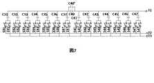
図7は、従来及び本願発明のスイッチ付容量を使ったDAコンバータの回路の一例である。端子T1を出力とし、端子T2をGND、端子T3を電源もしくは基準電圧につなぐことにより、スイッチS31〜S47及びS31’〜S47’の選択に応じT1に所望のアナログ電圧を出力する回路である。
従来容量値C31〜C37、C41〜C47はそれぞれ二進の重みをもたせる場合が多かった。
また、C41〜C47がMSB側の複数のビットであり、C41〜C47がLSB側の複数のビットである。よく知られているように、C40とC41’はC31〜C37合計をC41とほぼ等しくするようスケーリングするための容量であり、通常はC41の1〜2倍である。FIG. 7 shows an example of a conventional DA converter circuit using a switched capacitor according to the present invention. This is a circuit that outputs a desired analog voltage to T1 according to selection of switches S31 to S47 and S31 ′ to S47 ′ by connecting terminal T1 to output, terminal T2 to GND, and terminal T3 to a power supply or a reference voltage.
Conventional capacity values C31 to C37 and C41 to C47 often have binary weights, respectively.
C41 to C47 are a plurality of bits on the MSB side, and C41 to C47 are a plurality of bits on the LSB side. As is well known, C40 and C41 ′ are capacities for scaling the C31 to C37 sum to be approximately equal to C41, and are typically 1 to 2 times C41.
本願の場合、C31〜C37とC41〜C47を単位MOM容量とすることが、回路上の特徴である。In the present application, C31 to C37 and C41 to C47 are unit MOM capacities.
図8は本願第4の実施例である。C31〜C37とC41〜C47は1本のフィンガで構成されたMOM容量であり、スイッチS31〜S47とS31’〜S47’はMOSトランジスタで構成されたスイッチである。スイッチを図の縦方向に多段に並べることによりMOM容量と複数のスイッチを同一ピッチで並べることが出来る。この例ではDAコンバータへ与えられる上位3bitのデータを用いて、C41〜C47のMOM容量をスイッチで選択し、所望の出力電圧を得る。ここでその選択方法は、実施例1で述べた二進制御でも、温度計制御でも任意に選択できる。同様にDAコンバータへ与えられる下位3bitのデータを用いて、C31〜C37のMOM容量をスイッチで選択し、所望の出力電圧を得る。ここでその選択方法は、実施例1で述べた二進制御でも、温度計制御でも任意に選択できる(ゲート接続は図示せず)。この例はC40とC40’も同一の単位容量で構成した。このような構成の場合、下位側に若干の容量を追加してスケーリング値を合わせることが一般的に行われているので、図示はしないが、C31の左側にこの容量を容易に追加できる。FIG. 8 shows a fourth embodiment of the present application. C31 to C37 and C41 to C47 are MOM capacitors formed by one finger, and switches S31 to S47 and S31 'to S47' are switches formed by MOS transistors. By arranging switches in multiple stages in the vertical direction in the figure, it is possible to arrange MOM capacity and multiple switches at the same pitch. In this example, the upper 3 bits of data supplied to the DA converter is used to select the MOM capacities of C41 to C47 with a switch to obtain a desired output voltage. Here, the selection method can be arbitrarily selected by either the binary control described in the first embodiment or the thermometer control. Similarly, using the lower 3 bits of data supplied to the DA converter, the MOM capacities of C31 to C37 are selected by a switch to obtain a desired output voltage. Here, the selection method can be arbitrarily selected by the binary control described in the first embodiment or the thermometer control (the gate connection is not shown). In this example, C40 and C40 'are also configured with the same unit capacity. In the case of such a configuration, since it is generally performed to add a small capacity to the lower side to match the scaling value, this capacity can be easily added to the left side of C31, although not shown.
C37とC40’の間にあるのはシールド電極であり、端子T2のGNDへ接続されている。また通常S31〜S47はNチャネルMOSトランジスタで構成され、S31’〜S47’はPチャネルMOSトランジスタで構成されるが、バックゲート等は図示していない。共通ソースをそれぞれT2とT3に引き出す配線は、スイッチを構成するトランジスタの直上を上位の配線層を用いて構成することもできる。Between C37 and C40 'is a shield electrode, which is connected to the GND of terminal T2. In general, S31 to S47 are composed of N-channel MOS transistors, and S31 'to S47' are composed of P-channel MOS transistors, but the back gate and the like are not shown. Wirings that lead out the common source to T2 and T3, respectively, can also be configured using an upper wiring layer directly above the transistors that constitute the switch.
このようにMOM容量とスイッチを同一ピッチで並べることにより、極めて規則的に図7の回路をレイアウトすることが出来る。従来のように容量とスイッチを個別に作り、分離したりシールドしたりするスペースが不要になる分、高密度で実装可能であり、かつ相互干渉もない。さらに、スイッチS37とS41間、スイッチS37’とS41’間も同一ピッチでトランジスタを並べて配置することと、シールドを容量と同一ピッチで配置すること、および図の両端にダミー容量とダミースイッチを同一ピッチで配置する(図示せず)ことにより、全ての容量とスイッチの隣との環境を同一にすることが出来る。これにより、相対精度の向上が見込める。
単位MOM容量とスイッチの関係として、実施例1〜3の容量とスイッチを準用することもできる。また単位容量値やフィンガ本数は、要求されるビット数等に応じて任意に選択できる。スケーリング用のC40とC40’の位置も図8に限定せず、例えばC37側に付けるとか、C31の左側に付けるとか、ピッチを変えなければ、どこに置いても構わない。スイッチの個数も任意に増加することが可能であり、ADコンバータ等応用する際にさらに入力信号を印加するスイッチを追加することもできる。スイッチを構成するMOSトランジスタの極性は上記に限定されず、必要によりP,N並列にすることを含め、適宜選択すればよい。Thus, by arranging the MOM capacitors and the switches at the same pitch, the circuit of FIG. 7 can be laid out very regularly. Since the space for separating and shielding the capacitor and the switch is made separately as in the conventional case, it can be mounted at a high density and there is no mutual interference. Furthermore, between switches S37 and S41, between switches S37 'and S41', transistors are arranged side by side at the same pitch, shields are arranged at the same pitch as the capacitors, and dummy capacitors and dummy switches are the same at both ends of the figure. By arranging them at a pitch (not shown), the environment of all capacitors and the next to the switch can be made the same. Thereby, improvement of relative accuracy can be expected.
As the relationship between the unit MOM capacity and the switch, the capacity and switch of the first to third embodiments can be applied mutatis mutandis. The unit capacity value and the number of fingers can be arbitrarily selected according to the required number of bits. The positions of C40 and C40 ′ for scaling are not limited to those shown in FIG. 8, and may be placed anywhere as long as they are attached to the C37 side, the left side of C31, or the pitch is not changed. The number of switches can be arbitrarily increased, and a switch for applying an input signal can be further added when an AD converter or the like is applied. The polarity of the MOS transistor constituting the switch is not limited to the above, and may be appropriately selected including P and N parallel if necessary.
図9は第5の実施例であり、C40’を単位MOS容量の約1/2としたレイアウトの例である。つまりC40とC40’を合わせたスケーリング容量は単位容量の約1.5倍である。こうすると、第4の実施例より小さく作ることが出来る。FIG. 9 shows a fifth embodiment, which is an example of a layout in which C40 'is about 1/2 of the unit MOS capacitance. That is, the combined scaling capacity of C40 and C40 'is about 1.5 times the unit capacity. In this way, it can be made smaller than the fourth embodiment.
第10a図は従来及び本願発明のDフリップ・フロップ(以下DFFと言う)のゲート・レベル回路図であり、同図bはトランジスタ・レベルの回路図である。
同図cは本願の第6の実施例であり、同図a,bをレイアウトしたものである。その特徴は、ゲート4本の幅にあり、かつ各トランジスタ領域の両側はソースであり、電源VDDもしくはGNDに接続されるように並べたことを特徴にしている。このためこのDFFを横に並べる際に、両端のソースを共用することで、ゲート4本のピッチで連続して並べることが出来る。
なお図10cでは、最上段がNチャネルMOSトランジスタ、次がPチャネルMOSトランジスタ、次もPチャネルMOSトランジスタ、次はNチャネルMOSトランジスタ、次もNチャネルMOSトランジスタ、最下段はPチャネルMOSトランジスタである(バックゲート等は図示せず)。薄い灰色で示すゲート及びそれを厚い酸化膜上に引き出して配線として利用する部分と、濃い灰色で示す配線と、黒で示す別の層の配線で図10bの回路を結線したものである。
なお、図10cの縦方向のゲート幅は、必ずしも同一である必要はない。
本実施例は、ゲート4本のピッチでDFFをレイアウトできることを示す一例であり、その内部のトランジスタの位置と配線方法は、これ以外のレイアウトであっても構わない。FIG. 10a is a gate level circuit diagram of a conventional D flip-flop (hereinafter referred to as DFF) of the present invention, and FIG. 10b is a transistor level circuit diagram.
FIG. 7C shows the sixth embodiment of the present application, which is a layout of FIGS. The feature is that the width is four gates, and both sides of each transistor region are sources, and are arranged so as to be connected to the power supply VDD or GND. For this reason, when this DFF is arranged horizontally, it is possible to arrange them continuously at a pitch of four gates by sharing the sources at both ends.
In FIG. 10c, the top is an N-channel MOS transistor, the next is a P-channel MOS transistor, the next is a P-channel MOS transistor, the next is an N-channel MOS transistor, the next is an N-channel MOS transistor, and the bottom is a P-channel MOS transistor. (Back gate etc. not shown). The circuit shown in FIG. 10b is connected by a gate shown in light gray and a portion where the gate is drawn out on a thick oxide film and used as a wiring, a wiring shown in dark gray, and another layer of wiring shown in black.
Note that the vertical gate widths in FIG. 10c are not necessarily the same.
This embodiment is an example showing that a DFF can be laid out at a pitch of four gates, and the layout of transistors inside and the wiring method may be other than this.
図11は本願の第7の実施例であり、図9に相当するスイッチ付MOM容量と、図10cのDFFを8個並べて、接続したものである。本実施例の特徴は、容量とスイッチを同一ピッチで配置するのみならず、それを制御するロジック部の例であるDFFまでも同一ピッチで並べたことである。
本実施例では、容量2フィンガに対し、スイッチを構成するMOSトランジスタ4ゲートと、DFF 1個が同一ピッチで並べてある。このため、S42,S42’,S43,S43’と、S44,S44’,S45,S45’と、S46,S46’,S47,S47’はそれぞれ同一のDFFの出力信号で制御される。S41,S41’を二進制御とし、他を温度計制御するなどで、DAコンバータの上位3bitに応じて端子T1にDA変換出力を得ることが出来る。下位についても同様である。
また全体として幅を揃えるためC40’の構成を若干変えている。このような構成により、単位MOM容量のちょうど半分の容量を高精度に実現できる。
このような構成にすることにより、上記の効果に加え、ロジック回路と各スイッチを結ぶ配線領域が不要となり、さらに小さく作ることができる。両端にダミー容量とダミースイッチ、ダミーロジック・ゲートを置くことで、ロジックの配線を含め、全ての単位容量とスイッチの両隣が全く同一とすることが出来るので、相対精度が向上する。またロジックの負荷容量となる配線とスイッチの入力容量も全て等しくなるので、スイッチの切替タイミングも揃うという利点がある。FIG. 11 shows a seventh embodiment of the present application, in which a switch-equipped MOM capacitor corresponding to FIG. 9 and eight DFFs of FIG. 10c are arranged side by side. The feature of this embodiment is that not only the capacitors and the switches are arranged at the same pitch, but also DFFs, which are examples of the logic unit for controlling them, are arranged at the same pitch.
In this embodiment, for a capacitor 2 finger, 4 gates of MOS transistors constituting a switch and 1 DFF are arranged at the same pitch. For this reason, S42, S42 ′, S43, S43 ′, S44, S44 ′, S45, S45 ′ and S46, S46 ′, S47, S47 ′ are controlled by the same DFF output signal. By using binary control for S41 and S41 ′ and thermometer control for others, a DA conversion output can be obtained at the terminal T1 according to the upper 3 bits of the DA converter. The same applies to the lower level.
In addition, the configuration of C40 'is slightly changed to make the width as a whole. With such a configuration, a capacity that is exactly half the unit MOM capacity can be realized with high accuracy.
By adopting such a configuration, in addition to the above effects, a wiring region connecting the logic circuit and each switch is not necessary and can be made smaller. By placing dummy capacitors, dummy switches, and dummy logic gates at both ends, all unit capacitors and both sides of the switch, including the logic wiring, can be made exactly the same, thus improving relative accuracy. In addition, since the wiring that becomes the load capacity of the logic and the input capacity of the switch are all equal, there is an advantage that the switch switching timing is also aligned.
図11のMOM容量とスイッチのピッチの関係として、実施例1〜6のいずれを用いても良い。またビット数やスイッチの個数、極性等も適宜に選択できる。
本願発明の趣旨は、MOM容量とスイッチのピッチを同一、もしくは整数倍にすることであり、本実施例はさらにロジックまで同一もしくは整数倍のピッチとしたものである。
例えば、DFFを図の縦方向に2段配置して、適宜多層配線することで、ピッチを守ったまま、S42,S42’とS43,S43’と・・S47,S47’をそれぞれ異なる制御をすることもできる(図示せず)。
DFFに加え、スイッチの選択に関するロジックも同一ピッチで構成することもできる(図示せず)。DFF無しで、スイッチの選択に関するロジックのみを同一もしくは整数倍のピッチで並べることもできる。スイッチの選択に関するロジックの例としては、サーモメータ・コードへの変換ロジックや、ロジック信号の伝達遅れを概略等しくするための工夫などがある。As the relationship between the MOM capacity and the switch pitch in FIG. 11, any of the first to sixth embodiments may be used. In addition, the number of bits, the number of switches, polarity, and the like can be selected as appropriate.
The gist of the present invention is to make the pitch of the MOM capacitor and the switch the same or an integer multiple, and in this embodiment, the logic is further made the same or an integer multiple pitch.
For example, DFF is arranged in two stages in the vertical direction in the figure, and multilayer wiring is performed as appropriate, so that S42, S42 'and S43, S43', and S47, S47 'are controlled differently while keeping the pitch. (Not shown).
In addition to DFF, logic related to switch selection can also be configured with the same pitch (not shown). Without DFF, only the logic related to switch selection can be arranged at the same or integer multiple pitches. Examples of logic relating to switch selection include conversion logic to a thermometer code and a device for making transmission delays of logic signals approximately equal.
図12は本願の第8の実施例であり、図9に示したスイッチ付容量回路を2個用いて、インダクタL1とつないだものである。スイッチ付容量とインダクタL1で共振回路を構成しており、スイッチの選択によりデジタル的に、共振周波数を広範囲に変化させることが出来る。端子T1とT2を、高周波アナログ回路に接続し(図示せず)、デジタル的周波数可変フィルタを作ることが出来る。あるいは発振回路に接続して(図示せず)、デジタル的可変周波数発振器を作ることができる。FIG. 12 shows an eighth embodiment of the present application, in which two switched capacitance circuits shown in FIG. 9 are used and connected to the inductor L1. A resonant circuit is configured by the capacitor with the switch and the inductor L1, and the resonant frequency can be changed in a wide range digitally by selecting the switch. Terminals T1 and T2 can be connected to a high frequency analog circuit (not shown) to create a digital frequency variable filter. Alternatively, it can be connected to an oscillator circuit (not shown) to create a digital variable frequency oscillator.
図13は、図12のレイアウトの一例を図示したものである。FIG. 13 illustrates an example of the layout of FIG.
従来のLC共振回路の周波数調整には、主としてバラクタと呼ばれる印加直流電圧で容量が変化する素子を用い、アナログ電圧を制御していた。本実施例を用いると、デジタル的にスイッチのオン・オフを制御するだけで周波数制御することが出来、デジタル回路と親和性が良い。For adjusting the frequency of a conventional LC resonance circuit, an analog voltage is controlled by using an element whose capacitance changes mainly by an applied DC voltage called a varactor. When this embodiment is used, the frequency can be controlled simply by controlling the on / off of the switch digitally, and the compatibility with the digital circuit is good.
従来容量とスイッチが別々の部品として配置、配線されていたものを、本願発明ではまとめて「スイッチ付容量」と捉え直し、これらを同一もしくは整数倍のピッチで複数個規則的に並べるという発明である。特にLSIの微細化で配線間(MOM)容量の効率が高まったことにより、「スイッチ付容量」が実用可能になった。
本願は、これまでに述べてきた実施例に限定することなく、単位容量値、容量のフィンガ数、制御ビット数、制御ロジック回路等を適宜変更できることは言うまでもない。In the present invention, the conventional capacitor and switch arranged and wired as separate parts are collectively regarded as “capacitor with switch” in the present invention, and a plurality of these are regularly arranged at the same or integer multiple pitches. is there. In particular, with the miniaturization of LSIs, the efficiency of the inter-wiring (MOM) capacity has increased, making “capacitors with switches” practical.
Needless to say, the present application is not limited to the embodiments described so far, and the unit capacitance value, the number of capacitors, the number of control bits, the control logic circuit, and the like can be changed as appropriate.
C1〜C87 LSI内部の容量
S1〜S87,S1’〜S80’ MOSトランジスタによるスイッチ
L1 インダクタC1 to C87 LSI internal capacitance
S1-S87, S1'-S80 'MOS transistor switches
L1 inductor
Claims (17)
Translated fromJapanese前記容量の電極の長辺(フィンガー)の方向と、前記MOSトランジスタのゲートの長辺方向を同方向とし、これらを複数個並べる際の繰り返しピッチを同一もしくは他方の整数倍のピッチで連続して並べ、
前記各MOSトランジスタのドレイン電極は前記各容量の一端に接続し、かかる各MOSトランジスタのソース電極は隣接するMOSトランジスタのソース電極と共通構造とするとともに複数のMOSトランジスタ間で共通接続して第一の接続点とし、かかる各MOSトランジスタのゲート電極がスイッチの制御信号を受電し、前記容量の他端を第二の接続点としたことを特徴とするスイッチ付容量。In a circuit in which a plurality of capacitors using wiring inside the LSI and a switch composed of MOS transistors are connected to one end of each capacitor,
The direction of the long side (finger) of the electrode of the capacitor and the long side direction of the gate of the MOS transistor are the same direction, and the repetition pitch when arranging a plurality of these is continuously the same or the other integral multiple pitch continuously Line up,
The drain electrode of each MOS transistor is connected to one end of each capacitor, and the source electrode of each MOS transistor has a common structure with the source electrode of the adjacent MOS transistor and is commonly connected between a plurality of MOS transistors. A capacitor with a switch, wherein the gate electrode of each MOS transistor receives a switch control signal, and the other end of the capacitor is a second connection point.
An AD conversion circuit including the switched capacitor according toclaim 1 .
Priority Applications (3)
| Application Number | Priority Date | Filing Date | Title |
|---|---|---|---|
| JP2013196295AJP5899565B2 (en) | 2013-09-22 | 2013-09-22 | Capacitor with switch and circuit including capacitor with switch |
| US14/392,382US20160254822A1 (en) | 2013-09-22 | 2013-10-14 | Capacitor with Switch and Circuit Containing Capacitor with Switch |
| PCT/JP2013/077872WO2015040756A1 (en) | 2013-09-22 | 2013-10-14 | Capacitor with switch and circuit containing capacitor with switch |
Applications Claiming Priority (1)
| Application Number | Priority Date | Filing Date | Title |
|---|---|---|---|
| JP2013196295AJP5899565B2 (en) | 2013-09-22 | 2013-09-22 | Capacitor with switch and circuit including capacitor with switch |
Publications (3)
| Publication Number | Publication Date |
|---|---|
| JP2015062209A JP2015062209A (en) | 2015-04-02 |
| JP2015062209A5 JP2015062209A5 (en) | 2015-11-05 |
| JP5899565B2true JP5899565B2 (en) | 2016-04-06 |
Family
ID=52688436
Family Applications (1)
| Application Number | Title | Priority Date | Filing Date |
|---|---|---|---|
| JP2013196295AActiveJP5899565B2 (en) | 2013-09-22 | 2013-09-22 | Capacitor with switch and circuit including capacitor with switch |
Country Status (3)
| Country | Link |
|---|---|
| US (1) | US20160254822A1 (en) |
| JP (1) | JP5899565B2 (en) |
| WO (1) | WO2015040756A1 (en) |
Families Citing this family (4)
| Publication number | Priority date | Publication date | Assignee | Title |
|---|---|---|---|---|
| CN107204315B (en)* | 2016-03-17 | 2019-08-02 | 中国科学院苏州纳米技术与纳米仿生研究所 | Power device |
| WO2021061857A1 (en)* | 2019-09-23 | 2021-04-01 | Brigham Young University | Time-interleaved successive approximation register analog to digital converter with grouped digital to analog capacitors |
| JP7226470B2 (en) | 2021-04-26 | 2023-02-21 | セイコーエプソン株式会社 | electro-optical devices and electronics |
| US20240389486A1 (en)* | 2023-05-15 | 2024-11-21 | Taiwan Semiconductor Manufacturing Company Limited | Capacitor circuit providing self-adjusting capacitance and methods for forming the same |
Family Cites Families (5)
| Publication number | Priority date | Publication date | Assignee | Title |
|---|---|---|---|---|
| JP2002190738A (en)* | 2000-12-21 | 2002-07-05 | Fuji Electric Co Ltd | Digital-to-analog converter and analog-to-digital converter |
| JP3549499B2 (en)* | 2001-07-04 | 2004-08-04 | 松下電器産業株式会社 | Semiconductor integrated circuit device, D / A converter, and A / D converter |
| CN1953181B (en)* | 2005-10-21 | 2010-10-13 | 松下电器产业株式会社 | Analog-digital converter |
| US9024700B2 (en)* | 2008-02-28 | 2015-05-05 | Peregrine Semiconductor Corporation | Method and apparatus for use in digitally tuning a capacitor in an integrated circuit device |
| JP2013120857A (en)* | 2011-12-07 | 2013-06-17 | Renesas Electronics Corp | Semiconductor integrated circuit |
- 2013
- 2013-09-22JPJP2013196295Apatent/JP5899565B2/enactiveActive
- 2013-10-14WOPCT/JP2013/077872patent/WO2015040756A1/enactiveApplication Filing
- 2013-10-14USUS14/392,382patent/US20160254822A1/ennot_activeAbandoned
Also Published As
| Publication number | Publication date |
|---|---|
| JP2015062209A (en) | 2015-04-02 |
| WO2015040756A1 (en) | 2015-03-26 |
| US20160254822A1 (en) | 2016-09-01 |
Similar Documents
| Publication | Publication Date | Title |
|---|---|---|
| US10937730B2 (en) | Metal-on-metal capacitors | |
| US7787233B1 (en) | Multi-segment capacitor | |
| US7394416B2 (en) | Analog-digital converter | |
| US7639474B1 (en) | Multi-segment parallel wire capacitor | |
| JP5899565B2 (en) | Capacitor with switch and circuit including capacitor with switch | |
| JP2008226998A (en) | Semiconductor integrated circuit | |
| US7403147B2 (en) | Precision capacitor array | |
| US20100033259A1 (en) | Semiconductor integrated circuit device | |
| US20190378793A1 (en) | Integration of guard ring with passive components | |
| US7994604B2 (en) | Using floating fill metal to reduce power use for proximity communication | |
| JP2015002247A (en) | Semiconductor device | |
| Karmokar et al. | Constructive placement and routing for common-centroid capacitor arrays in binary-weighted and split DACs | |
| US20170093362A1 (en) | Metal-oxide-metal (mom) capacitor with reduced magnetic coupling to neighboring circuit and high series resonance frequency | |
| US10992261B2 (en) | Semiconductor integrated circuitry | |
| US8502348B2 (en) | Differential varactor device | |
| JP4676894B2 (en) | Resonator type oscillator and tuning capacitor circuit | |
| US9165925B2 (en) | Structures and methods for ring oscillator fabrication | |
| JP2011035210A (en) | Semiconductor integrated circuit, and layout method for the same | |
| JP5126333B2 (en) | Resonator type oscillator and tuning capacitor circuit | |
| US12369391B2 (en) | Layout pattern of semiconductor varactor and forming method thereof | |
| Karmokar | Automated Layout of Analog Arrays in Advanced Technology Nodes | |
| CN112582538A (en) | Capacitor structure | |
| JP2013201657A (en) | Electronic circuit |
Legal Events
| Date | Code | Title | Description |
|---|---|---|---|
| A871 | Explanation of circumstances concerning accelerated examination | Free format text:JAPANESE INTERMEDIATE CODE: A871 Effective date:20150824 | |
| A521 | Request for written amendment filed | Free format text:JAPANESE INTERMEDIATE CODE: A523 Effective date:20150824 | |
| A621 | Written request for application examination | Free format text:JAPANESE INTERMEDIATE CODE: A621 Effective date:20150824 | |
| A975 | Report on accelerated examination | Free format text:JAPANESE INTERMEDIATE CODE: A971005 Effective date:20151019 | |
| A131 | Notification of reasons for refusal | Free format text:JAPANESE INTERMEDIATE CODE: A131 Effective date:20151124 | |
| A521 | Request for written amendment filed | Free format text:JAPANESE INTERMEDIATE CODE: A523 Effective date:20160102 | |
| TRDD | Decision of grant or rejection written | ||
| A01 | Written decision to grant a patent or to grant a registration (utility model) | Free format text:JAPANESE INTERMEDIATE CODE: A01 Effective date:20160209 | |
| A61 | First payment of annual fees (during grant procedure) | Free format text:JAPANESE INTERMEDIATE CODE: A61 Effective date:20160213 | |
| R150 | Certificate of patent or registration of utility model | Ref document number:5899565 Country of ref document:JP Free format text:JAPANESE INTERMEDIATE CODE: R150 | |
| A521 | Request for written amendment filed | Free format text:JAPANESE INTERMEDIATE CODE: A523 Effective date:20161218 |