JP5896412B2 - Fuse element for protection element and circuit protection element using the same - Google Patents
Fuse element for protection element and circuit protection element using the sameDownload PDFInfo
- Publication number
- JP5896412B2 JP5896412B2JP2012113369AJP2012113369AJP5896412B2JP 5896412 B2JP5896412 B2JP 5896412B2JP 2012113369 AJP2012113369 AJP 2012113369AJP 2012113369 AJP2012113369 AJP 2012113369AJP 5896412 B2JP5896412 B2JP 5896412B2
- Authority
- JP
- Japan
- Prior art keywords
- alloy
- melting point
- fuse element
- bonding
- coating material
- Prior art date
- Legal status (The legal status is an assumption and is not a legal conclusion. Google has not performed a legal analysis and makes no representation as to the accuracy of the status listed.)
- Active
Links
- 238000002844meltingMethods0.000claimsdescription110
- 230000008018meltingEffects0.000claimsdescription109
- 239000000463materialSubstances0.000claimsdescription104
- 239000000758substrateSubstances0.000claimsdescription72
- 238000000576coating methodMethods0.000claimsdescription57
- 239000011248coating agentSubstances0.000claimsdescription56
- 239000000956alloySubstances0.000claimsdescription49
- 229910045601alloyInorganic materials0.000claimsdescription43
- 230000004907fluxEffects0.000claimsdescription33
- 239000002184metalSubstances0.000claimsdescription30
- 229910052751metalInorganic materials0.000claimsdescription30
- 239000007769metal materialSubstances0.000claimsdescription29
- 239000002131composite materialSubstances0.000claimsdescription28
- 230000001681protective effectEffects0.000claimsdescription26
- 238000005304joiningMethods0.000claimsdescription25
- 238000010438heat treatmentMethods0.000claimsdescription19
- 238000000034methodMethods0.000claimsdescription14
- 239000002356single layerSubstances0.000claimsdescription9
- 238000004519manufacturing processMethods0.000claimsdescription8
- 238000010030laminatingMethods0.000claimsdescription5
- BDAGIHXWWSANSR-UHFFFAOYSA-Nmethanoic acidNatural productsOC=OBDAGIHXWWSANSR-UHFFFAOYSA-N0.000claimsdescription4
- 238000004806packaging method and processMethods0.000claimsdescription4
- 230000009467reductionEffects0.000claimsdescription4
- 229910017944Ag—CuInorganic materials0.000claimsdescription3
- 229910001152Bi alloyInorganic materials0.000claimsdescription3
- 229910000846In alloyInorganic materials0.000claimsdescription3
- 229910020220Pb—SnInorganic materials0.000claimsdescription3
- 229910020836Sn-AgInorganic materials0.000claimsdescription3
- 229910020830Sn-BiInorganic materials0.000claimsdescription3
- 229910020888Sn-CuInorganic materials0.000claimsdescription3
- 229910020935Sn-SbInorganic materials0.000claimsdescription3
- 229910020994Sn-ZnInorganic materials0.000claimsdescription3
- 229910020988Sn—AgInorganic materials0.000claimsdescription3
- 229910018728Sn—BiInorganic materials0.000claimsdescription3
- 229910019204Sn—CuInorganic materials0.000claimsdescription3
- 229910008757Sn—SbInorganic materials0.000claimsdescription3
- 229910009069Sn—ZnInorganic materials0.000claimsdescription3
- 229910009071Sn—Zn—BiInorganic materials0.000claimsdescription3
- 229910007570Zn-AlInorganic materials0.000claimsdescription3
- 229910052732germaniumInorganic materials0.000claimsdescription3
- 229910052737goldInorganic materials0.000claimsdescription3
- 229910052759nickelInorganic materials0.000claimsdescription3
- OSWFIVFLDKOXQC-UHFFFAOYSA-N4-(3-methoxyphenyl)anilineChemical compoundCOC1=CC=CC(C=2C=CC(N)=CC=2)=C1OSWFIVFLDKOXQC-UHFFFAOYSA-N0.000claimsdescription2
- UFHFLCQGNIYNRP-UHFFFAOYSA-NHydrogenChemical compound[H][H]UFHFLCQGNIYNRP-UHFFFAOYSA-N0.000claimsdescription2
- 230000004913activationEffects0.000claimsdescription2
- 235000019253formic acidNutrition0.000claimsdescription2
- 239000001257hydrogenSubstances0.000claimsdescription2
- 229910052739hydrogenInorganic materials0.000claimsdescription2
- 238000002360preparation methodMethods0.000claimsdescription2
- 229910052733galliumInorganic materials0.000claims2
- 230000008569processEffects0.000description8
- 229910001316Ag alloyInorganic materials0.000description5
- 239000000919ceramicSubstances0.000description5
- 230000000052comparative effectEffects0.000description5
- 239000010410layerSubstances0.000description5
- 238000003466weldingMethods0.000description5
- 239000011521glassSubstances0.000description4
- 230000002093peripheral effectEffects0.000description3
- 230000005856abnormalityEffects0.000description2
- PNEYBMLMFCGWSK-UHFFFAOYSA-Naluminium oxideInorganic materials[O-2].[O-2].[O-2].[Al+3].[Al+3]PNEYBMLMFCGWSK-UHFFFAOYSA-N0.000description2
- 239000011162core materialSubstances0.000description2
- 229910000743fusible alloyInorganic materials0.000description2
- 239000004033plasticSubstances0.000description2
- 229920005989resinPolymers0.000description2
- 239000011347resinSubstances0.000description2
- 238000005476solderingMethods0.000description2
- JYEUMXHLPRZUAT-UHFFFAOYSA-N1,2,3-triazineChemical compoundC1=CN=NN=C1JYEUMXHLPRZUAT-UHFFFAOYSA-N0.000description1
- XQUPVDVFXZDTLT-UHFFFAOYSA-N1-[4-[[4-(2,5-dioxopyrrol-1-yl)phenyl]methyl]phenyl]pyrrole-2,5-dioneChemical compoundO=C1C=CC(=O)N1C(C=C1)=CC=C1CC1=CC=C(N2C(C=CC2=O)=O)C=C1XQUPVDVFXZDTLT-UHFFFAOYSA-N0.000description1
- RSWGJHLUYNHPMX-UHFFFAOYSA-NAbietic-SaeureNatural productsC12CCC(C(C)C)=CC2=CCC2C1(C)CCCC2(C)C(O)=ORSWGJHLUYNHPMX-UHFFFAOYSA-N0.000description1
- 206010000369AccidentDiseases0.000description1
- 239000004593EpoxySubstances0.000description1
- 229920000106Liquid crystal polymerPolymers0.000description1
- 239000004977Liquid-crystal polymers (LCPs)Substances0.000description1
- KHPCPRHQVVSZAH-HUOMCSJISA-NRosinNatural productsO(C/C=C/c1ccccc1)[C@H]1[C@H](O)[C@@H](O)[C@@H](O)[C@@H](CO)O1KHPCPRHQVVSZAH-HUOMCSJISA-N0.000description1
- 239000004809TeflonSubstances0.000description1
- 229920006362Teflon®Polymers0.000description1
- 230000002159abnormal effectEffects0.000description1
- 230000003213activating effectEffects0.000description1
- 230000002411adverseEffects0.000description1
- 238000005452bendingMethods0.000description1
- 230000015556catabolic processEffects0.000description1
- 229910010293ceramic materialInorganic materials0.000description1
- 230000008859changeEffects0.000description1
- 238000005253claddingMethods0.000description1
- 239000004020conductorSubstances0.000description1
- 230000007547defectEffects0.000description1
- 230000002950deficientEffects0.000description1
- 238000006731degradation reactionMethods0.000description1
- 210000001787dendriteAnatomy0.000description1
- 238000009713electroplatingMethods0.000description1
- 239000003822epoxy resinSubstances0.000description1
- 230000003628erosive effectEffects0.000description1
- 239000007789gasSubstances0.000description1
- 230000020169heat generationEffects0.000description1
- 230000001678irradiating effectEffects0.000description1
- 229910001416lithium ionInorganic materials0.000description1
- 238000005259measurementMethods0.000description1
- 239000000155meltSubstances0.000description1
- 230000004048modificationEffects0.000description1
- 238000012986modificationMethods0.000description1
- 238000013021overheatingMethods0.000description1
- 230000000149penetrating effectEffects0.000description1
- 238000007747platingMethods0.000description1
- 229920003192poly(bis maleimide)Polymers0.000description1
- 229920000647polyepoxidePolymers0.000description1
- 238000012360testing methodMethods0.000description1
- KHPCPRHQVVSZAH-UHFFFAOYSA-Ntrans-cinnamyl beta-D-glucopyranosideNatural productsOC1C(O)C(O)C(CO)OC1OCC=CC1=CC=CC=C1KHPCPRHQVVSZAH-UHFFFAOYSA-N0.000description1
- 239000012808vapor phaseSubstances0.000description1
- 238000005491wire drawingMethods0.000description1
Images


Classifications
- H—ELECTRICITY
- H01—ELECTRIC ELEMENTS
- H01H—ELECTRIC SWITCHES; RELAYS; SELECTORS; EMERGENCY PROTECTIVE DEVICES
- H01H37/00—Thermally-actuated switches
- H01H37/02—Details
- H01H37/32—Thermally-sensitive members
- H—ELECTRICITY
- H01—ELECTRIC ELEMENTS
- H01H—ELECTRIC SWITCHES; RELAYS; SELECTORS; EMERGENCY PROTECTIVE DEVICES
- H01H37/00—Thermally-actuated switches
- H01H37/74—Switches in which only the opening movement or only the closing movement of a contact is effected by heating or cooling
- H01H37/76—Contact member actuated by melting of fusible material, actuated due to burning of combustible material or due to explosion of explosive material
- H01H37/761—Contact member actuated by melting of fusible material, actuated due to burning of combustible material or due to explosion of explosive material with a fusible element forming part of the switched circuit
- H—ELECTRICITY
- H01—ELECTRIC ELEMENTS
- H01H—ELECTRIC SWITCHES; RELAYS; SELECTORS; EMERGENCY PROTECTIVE DEVICES
- H01H37/00—Thermally-actuated switches
- H01H37/02—Details
- H01H37/04—Bases; Housings; Mountings
- H—ELECTRICITY
- H01—ELECTRIC ELEMENTS
- H01H—ELECTRIC SWITCHES; RELAYS; SELECTORS; EMERGENCY PROTECTIVE DEVICES
- H01H37/00—Thermally-actuated switches
- H01H37/02—Details
- H01H37/64—Contacts
- H—ELECTRICITY
- H01—ELECTRIC ELEMENTS
- H01H—ELECTRIC SWITCHES; RELAYS; SELECTORS; EMERGENCY PROTECTIVE DEVICES
- H01H69/00—Apparatus or processes for the manufacture of emergency protective devices
- H01H69/02—Manufacture of fuses
- H—ELECTRICITY
- H01—ELECTRIC ELEMENTS
- H01H—ELECTRIC SWITCHES; RELAYS; SELECTORS; EMERGENCY PROTECTIVE DEVICES
- H01H69/00—Apparatus or processes for the manufacture of emergency protective devices
- H01H69/02—Manufacture of fuses
- H01H69/022—Manufacture of fuses of printed circuit fuses
- H—ELECTRICITY
- H01—ELECTRIC ELEMENTS
- H01H—ELECTRIC SWITCHES; RELAYS; SELECTORS; EMERGENCY PROTECTIVE DEVICES
- H01H85/00—Protective devices in which the current flows through a part of fusible material and this current is interrupted by displacement of the fusible material when this current becomes excessive
- H01H85/02—Details
- H01H85/0241—Structural association of a fuse and another component or apparatus
- H—ELECTRICITY
- H01—ELECTRIC ELEMENTS
- H01H—ELECTRIC SWITCHES; RELAYS; SELECTORS; EMERGENCY PROTECTIVE DEVICES
- H01H37/00—Thermally-actuated switches
- H01H37/02—Details
- H01H37/04—Bases; Housings; Mountings
- H01H2037/046—Bases; Housings; Mountings being soldered on the printed circuit to be protected
- H—ELECTRICITY
- H01—ELECTRIC ELEMENTS
- H01H—ELECTRIC SWITCHES; RELAYS; SELECTORS; EMERGENCY PROTECTIVE DEVICES
- H01H85/00—Protective devices in which the current flows through a part of fusible material and this current is interrupted by displacement of the fusible material when this current becomes excessive
- H01H85/02—Details
- H01H85/0241—Structural association of a fuse and another component or apparatus
- H01H2085/0275—Structural association with a printed circuit board
- H—ELECTRICITY
- H01—ELECTRIC ELEMENTS
- H01H—ELECTRIC SWITCHES; RELAYS; SELECTORS; EMERGENCY PROTECTIVE DEVICES
- H01H85/00—Protective devices in which the current flows through a part of fusible material and this current is interrupted by displacement of the fusible material when this current becomes excessive
- H01H85/48—Protective devices wherein the fuse is carried or held directly by the base
- Y—GENERAL TAGGING OF NEW TECHNOLOGICAL DEVELOPMENTS; GENERAL TAGGING OF CROSS-SECTIONAL TECHNOLOGIES SPANNING OVER SEVERAL SECTIONS OF THE IPC; TECHNICAL SUBJECTS COVERED BY FORMER USPC CROSS-REFERENCE ART COLLECTIONS [XRACs] AND DIGESTS
- Y10—TECHNICAL SUBJECTS COVERED BY FORMER USPC
- Y10T—TECHNICAL SUBJECTS COVERED BY FORMER US CLASSIFICATION
- Y10T29/00—Metal working
- Y10T29/49—Method of mechanical manufacture
- Y10T29/49002—Electrical device making
- Y10T29/49107—Fuse making
Landscapes
- Engineering & Computer Science (AREA)
- Manufacturing & Machinery (AREA)
- Chemical & Material Sciences (AREA)
- Combustion & Propulsion (AREA)
- Power Engineering (AREA)
- Physics & Mathematics (AREA)
- Thermal Sciences (AREA)
- Fuses (AREA)
Description
Translated fromJapanese本発明は、複合金属材からなる保護素子用ヒューズ素子およびそれを利用した電気・電子機器の回路保護素子に関する。 The present invention relates to a fuse element for a protection element made of a composite metal material and a circuit protection element of an electric / electronic device using the fuse element.
近年、モバイル機器など小型電子機器の急速な普及に伴い、搭載する電源の保護回路に実装される保護素子も小型薄型のものが使用されている。例えば、二次電池パックの保護回路には、表面実装部品(SMD)のチップ保護素子が好適に利用される。これらチップ保護素子には、被保護機器の過電流により生ずる過大発熱を検知し、または周囲温度の異常過熱に感応して、所定条件でヒューズを作動させ電気回路を遮断する非復帰型保護素子がある。該保護素子は、機器の安全を図るために、保護回路が機器に生ずる異常を検知すると信号電流により抵抗素子を発熱させ、その発熱で可融性の合金材からなるヒューズ素子(ヒューズエレメントとも言う)を溶断させて回路を遮断するか、あるいは過電流によってヒューズ素子を溶断させて回路を遮断できる。例えば、特許文献1および特許文献2には、異常時に発熱する抵抗素子をセラミックス基板などの絶縁基板上に設けた保護素子と、この保護素子を利用してLiイオン二次電池の過充電モードで電極表面に生成したデンドライトによる性能劣化などに起因する発火事故を防止する保護装置が開示されている。 In recent years, with the rapid spread of small electronic devices such as mobile devices, small and thin protective elements mounted on a protection circuit for a power supply to be mounted are used. For example, a surface protection component (SMD) chip protection element is preferably used for the protection circuit of the secondary battery pack. These chip protection elements include a non-recoverable protection element that detects excessive heat generated due to overcurrent of the device to be protected, or responds to abnormal overheating of the ambient temperature, and activates the fuse under predetermined conditions to shut off the electric circuit. is there. In order to protect the safety of the device, the protection element causes the resistance element to generate heat by a signal current when an abnormality occurring in the device is detected, and the heat generation causes a fuse element made of a fusible alloy material (also referred to as a fuse element). ) Can be cut off to cut off the circuit, or the fuse element can be cut off by overcurrent to cut off the circuit. For example, Patent Document 1 and Patent Document 2 disclose a protection element in which a resistance element that generates heat in an abnormality is provided on an insulating substrate such as a ceramic substrate, and an overcharge mode of a Li ion secondary battery using this protection element. A protective device for preventing a fire accident caused by performance degradation due to dendrite generated on the electrode surface is disclosed.
従来、上述したチップ保護素子のヒューズ素子を構成する可融性合金材は、セラミックス基板など絶縁基板の上に形成したパターン電極にレーザー溶接などの接合手段により取り付けられていた。レーザー溶接は、個片のヒューズ素子をパターン電極に確実に接合するために適した工法ではあるが、高価なレーザー溶接機を必要とし、個々の接合箇所にレーザーを局部照射しながら作業するため、複数のヒューズ素子を一括接合することができず、作業時間を要し必ずしも生産効率の高い方法ではなかった。また、特に平板状のヒューズ素子を絶縁基板のパターン電極と接合する場合には、レーザー照射熱によってヒューズ素子全体が溶融してしまわないようにヒューズ素子の周縁部にレーザーをポイント照射する必要があり、ヒューズ素子板の中央部分はパターン電極が在ってもこれを接合に利用することが難しい。このためヒューズ素子とパターン電極との接触面全面を接合面とすることができず、電気抵抗や接続強度の観点から最適とは言えない。 Conventionally, the fusible alloy material constituting the fuse element of the chip protection element described above has been attached to a pattern electrode formed on an insulating substrate such as a ceramic substrate by a joining means such as laser welding. Laser welding is a method suitable for reliably joining individual fuse elements to the pattern electrode, but requires an expensive laser welding machine and works while locally irradiating the laser at each joint location. A plurality of fuse elements could not be joined together, requiring work time, and not necessarily a method with high production efficiency. In particular, when a flat fuse element is joined to the pattern electrode on the insulating substrate, it is necessary to irradiate the periphery of the fuse element with a point to prevent the entire fuse element from being melted by the laser irradiation heat. In the central part of the fuse element plate, it is difficult to use the pattern electrode for bonding even if there is a pattern electrode. For this reason, the entire contact surface between the fuse element and the pattern electrode cannot be used as a bonding surface, which is not optimal from the viewpoint of electrical resistance and connection strength.
さらに、保護素子のヒューズ素子や基板電極を含む基板などの接合部品の小型化・薄型化の進展に伴い、より薄板のヒューズ素子を用いた場合には、レーザー熱によって溶接後のヒューズ素子が過熱変形したり、レーザー照射部位が過度に盛り上がって局部的に厚くなったりしてエレメント取付の出来ばえが悪くなる欠点があった。このため後工程で基板上のヒューズエレメントをキャップ状蓋体で覆って被覆する際、ヒューズ素子の変形が著しい場合には、キャップ状蓋体を絶縁基板に水平に取り付けることができなかったり、所定の取り付け位置からずれたりして蓋体の載置作業が妨げられ組立不良の原因となるなど好ましくない。 In addition, with the progress of miniaturization and thinning of joining parts such as protective element fuse elements and substrates including substrate electrodes, when a thinner fuse element is used, the fuse element after welding is overheated by laser heat. There was a defect that the element mounting was poor because it was deformed or the laser irradiation part was excessively raised and thickened locally. For this reason, when the fuse element on the substrate is covered and covered with a cap-shaped lid in a subsequent process, if the fuse element is significantly deformed, the cap-shaped lid cannot be mounted horizontally on the insulating substrate, It is not preferable because it may be displaced from the mounting position of the cover, hindering the mounting operation of the lid and causing a defective assembly.
特許文献1:特開2008−112735号公報
特許文献2:特開2011−034755号公報Patent Document 1: Japanese Patent Application Laid-Open No. 2008-1112735 Patent Document 2: Japanese Patent Application Laid-Open No. 2011-034755
したがって、本発明の目的は、上述の問題点を解消するために提案されたものであり、生産効率を向上でき、保護素子のヒューズ素子やパターン電極を含む基板など接合部品の小型薄型化に対応可能な複合金属材からなる保護素子用ヒューズ素子およびそれを利用した電気・電子機器の回路保護素子を提供することを目的とする。 Therefore, the object of the present invention is proposed to solve the above-mentioned problems, can improve the production efficiency, and cope with the miniaturization and thinning of joint parts such as a protective element fuse element and a substrate including a pattern electrode. An object of the present invention is to provide a fuse element for a protective element made of a composite metal material and a circuit protective element for an electric / electronic device using the same.
本発明によると、接合作業温度で溶融しない第1の融点温度を有する可融性金属からなる少なくとも単層の高融点ベース材と、接合作業温度で溶融可能な第2の融点温度を有する可融性金属からなる少なくとも単層の低融点被覆材とを積層した複合金属材を用いたことを特徴とする保護素子用ヒューズ素子が提供される。前記ヒューズ素子は、接合作業温度で溶融しない第1の融点温度を有する可融性金属からなる平板状または棒状の高融点ベース材の表面に、接合作業温度で溶融可能な第2の融点温度を有する可融性金属からなる低融点被覆材を設けた複合金属材であり、高融点ベース材が平板状の場合は、ベース材板面の少なくとも片側に低融点被覆材を設け、高融点ベース材が棒状の場合は、ベース材の周壁面に低融点被覆材を設ける。 According to the present invention, at least a single-layer high melting point base material made of a fusible metal having a first melting point temperature that does not melt at the joining operation temperature, and a fusible member having a second melting point temperature that can be melted at the joining operation temperature. Provided is a fuse element for a protective element, which uses a composite metal material in which at least a single-layer low melting point coating material made of a conductive metal is laminated. The fuse element has a second melting point temperature that can be melted at the joining operation temperature on the surface of a flat or rod-shaped high melting point base material made of a fusible metal having a first melting point temperature that does not melt at the joining operation temperature. A composite metal material provided with a low melting point coating material made of a fusible metal, and when the high melting point base material is a flat plate, a low melting point coating material is provided on at least one side of the base material plate surface. In the case of a rod shape, a low melting point coating material is provided on the peripheral wall surface of the base material.
本発明の別の観点よると、上記様態のヒューズ素子を利用した回路保護素子が提供される。本発明に係る回路保護素子は、前記ヒューズ素子とパターン電極を有する絶縁基板とを準備する準備工程、絶縁基板に接合フラックスを塗布する接合フラックス塗布工程、接合フラックスを塗布した絶縁基板のパターン電極とヒューズ素子の低融点被覆材とを互いに接触させて絶縁基板に載置するマウント工程、ヒューズ素子を載置した絶縁基板を183℃以上280℃未満の接合作業温度で低融点被覆材を溶融させてパターン電極に一括接合させる接合工程、接合したヒューズ素子に動作用の溶断フラックスを塗布する溶断フラックス塗布工程、溶断フラックスを塗布した絶縁基板上のヒューズ素子をキャップ状蓋体で覆ってパッケージングするパッケージング工程により組み立てられたことを特徴とする。すなわち、本発明に係る保護素子用ヒューズ素子は、絶縁基板の表面に設けたパターン電極に接合され、回路保護素子のヒューズエレメントとして使用される。該ヒューズ素子は、予め接合フラックスを塗布した絶縁基板のパターン電極とヒューズ素子の低融点被覆材とを互いに接触させて絶縁基板に載置され、前述の接合作業温度で低融点被覆材を溶融させることによりパターン電極に一括接合される。溶融した低融点被覆材は高融点ベース材とパターン電極とを接合させる。高融点ベース材は、接合作業温度で溶融しないので形状を保ったままパターン電極に固着され、所定の動作温度を損なうことなく所定条件で溶断するヒューズエレメントとなる。その後、固着したヒューズ素子に溶断フラックスを塗布し、基板上のヒューズ素子をキャップ状蓋体で覆ってパッケージングされて回路保護素子を形成する。 According to another aspect of the present invention, a circuit protection element using the fuse element of the above aspect is provided. A circuit protection element according to the present invention includes a preparation step of preparing the fuse element and an insulating substrate having a pattern electrode, a bonding flux applying step of applying a bonding flux to the insulating substrate, a pattern electrode of the insulating substrate coated with the bonding flux, A mounting step in which the low melting point coating material of the fuse element is brought into contact with each other and placed on the insulating substrate, and the low melting point coating material is melted at a bonding operation temperature of 183 ° C. or more and less than 280 ° C. A bonding process for collectively bonding to a pattern electrode, a fusing flux application process for applying a fusing flux for operation to the bonded fuse elements, and a package in which a fuse element on an insulating substrate coated with fusing flux is covered with a cap-shaped lid and packaged It is characterized by having been assembled by a bending process. That is, the fuse element for a protection element according to the present invention is joined to a pattern electrode provided on the surface of an insulating substrate and used as a fuse element of a circuit protection element. The fuse element is placed on the insulating substrate in such a manner that the pattern electrode of the insulating substrate to which the bonding flux is previously applied and the low melting point coating material of the fuse element are brought into contact with each other, and the low melting point coating material is melted at the above-described bonding operation temperature. As a result, the pattern electrodes are collectively bonded. The molten low melting point coating material joins the high melting point base material and the pattern electrode. Since the high melting point base material does not melt at the joining operation temperature, the high melting point base material is fixed to the pattern electrode while maintaining its shape, and becomes a fuse element that melts under predetermined conditions without impairing the predetermined operating temperature. Thereafter, a fusing flux is applied to the fixed fuse element, and the fuse element on the substrate is covered with a cap-shaped lid and packaged to form a circuit protection element.
本発明に係る回路保護素子は、絶縁基板と、該絶縁基板の表面に設けた複数のパターン電極と、このパターン電極に電気接続したヒューズ素子とを備え、ヒューズ素子は、接合作業温度で溶融しない第1の融点温度を有する可融性金属からなる少なくとも1つの高融点ベース材と、接合作業温度で溶融可能な第2の融点温度を有する可融性金属からなる少なくとも1つの低融点被覆材とを積層して成る複合金属材を用いたことを特徴とする保護素子が提供される。該保護素子の絶縁基板には必要に応じて抵抗発熱素子を設けてもよい。 A circuit protection element according to the present invention includes an insulating substrate, a plurality of pattern electrodes provided on the surface of the insulating substrate, and a fuse element electrically connected to the pattern electrode, and the fuse element does not melt at the bonding operation temperature. At least one high melting point base material made of a fusible metal having a first melting point temperature, and at least one low melting point coating material made of a fusible metal having a second melting point temperature that can be melted at the joining operation temperature; A protective element characterized by using a composite metal material formed by laminating layers is provided. A resistance heating element may be provided on the insulating substrate of the protection element as necessary.
本発明のヒューズ素子を用いることで、多数のヒューズ素子をリフロー工法により赤外線方式、熱風方式、VPS(ベーパーフェーズソルダリング)方式を含む各種リフロー炉、高温バッチ炉、温風ヒータ、ホットプレートなどを用いて一括接合することができ、生産効率を高めてより経済的に回路保護素子を生産することが可能となる。同時にヒューズ素子とパターン電極との接触面全面を接合できるので、接合面(接合代)をより広く取ることができ、接合面積を広くして電気抵抗を低減するとともに接合強度を向上する。 By using the fuse element of the present invention, various reflow furnaces such as an infrared system, a hot air system, a VPS (vapor phase soldering) system, a high temperature batch furnace, a hot air heater, a hot plate, etc. Therefore, it is possible to produce a circuit protection element more economically by increasing the production efficiency. At the same time, since the entire contact surface between the fuse element and the pattern electrode can be bonded, the bonding surface (bonding margin) can be increased, and the bonding area can be increased to reduce the electrical resistance and improve the bonding strength.
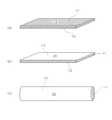
本発明に係る保護素子用ヒューズ素子は、図1に示すように、接合作業温度で溶融しない第1の融点温度を有する可融性金属からなる少なくとも単層の高融点ベース材11と、接合作業温度で溶融可能な第2の融点温度を有する可融性金属からなる少なくとも単層の低融点被覆材12とを積層した複合金属材を用いたことを特徴としている。この保護素子用ヒューズ素子には、高融点ベース材11として183℃以上280℃未満の接合作業温度において溶融しない可融性金属、例えば20Sn−80Au合金、55Sn−45Sb合金、Pbを80質量%以上含有したPb−Sn合金などの合金材が好適に利用できる。そして平板状または棒状の前記高融点ベース材11の表面に、該接合作業温度において溶融可能な可融性金属、例えばSn−Ag合金、Sn−Bi合金、Sn−Cu合金、Sn−Zn合金、Sn−Sb合金、Sn−Ag−Bi合金、Sn−Ag−Cu合金、Sn−Ag−In合金、Sn−Zn−Al合金、Sn−Zn−Bi合金または前記Sn基合金にAu、Ni、Ge、Gaをさらに添加した合金材などの低融点被覆材12を固着した複合金属材によって本発明に係る保護素子用ヒューズ素子を構成する。高融点ベース材11が平板状の場合は、該ベース材板面の少なくとも片側に低融点被覆材12を層状に設け、高融点ベース材11が棒状の場合は、該ベース材の外周面に低融点被覆材12を設ける。なお、上述の高融点ベース材11の表面に低融点被覆材12を設ける手段は、特に限定されず高融点ベース材11に低融点被覆材12を固着できればよい。例えば、低融点被覆材12はクラッド、めっき、溶融コート、圧着、ロジンなどの可融性樹脂による接着などの手段で高融点ベース材11の表面に固着できる。また、本発明に係る保護素子用ヒューズ素子は、積層面に予め接合フラックスを内蔵させた複合金属材としてもよい。 As shown in FIG. 1, a fuse element for a protective element according to the present invention includes at least a single-layer high-melting
さらに、上述した本発明に係る保護素子用ヒューズ素子は、図2に示すように、耐熱性の絶縁基板23の表面に設けた導電性部材からなるパターン電極24に溶融接合され回路保護素子のヒューズエレメント25として使用される。本発明に係る保護素子用ヒューズ素子がヒューズエレメントとして正常に機能するためには、接合前におけるヒューズ素子25の総厚または直径に対して低融点被覆材22の厚みが1%以上20%以下になるようにヒューズ素子25を成形しておく必要があり、より好適には前記厚みが5%以上15%以下になるようにヒューズ素子25を成形しておくとよい。さらにヒューズ素子25を搭載する回路保護素子の小型化・薄型化の観点から、接合前におけるヒューズ素子25の総厚または直径は64μm以上300μm以下とするのが望ましく、より好適には前記総厚または直径が85μm以上115μm以下となるようにヒューズ素子25を成形しておくとよい。例えば、接合前におけるヒューズ素子25の板厚が総厚100μmの場合には、低融点被覆材22の合計の厚さが5μm〜15μmの範囲となるように形成しておくのが好ましい。前記厚みが20%を超えると、ヒューズエレメント25を構成する高融点ベース材21の溶融温度や内部抵抗値などが変動したり、過剰に残留した低融点接合層や電極食われ現象によってヒューズエレメント25が接合剥離したりして回路保護素子の信頼性に悪影響をおよぼす。また、前記厚みが1%未満であると、高融点ベース材21をパターン電極24に充分に接合することができない。 Further, as shown in FIG. 2, the fuse element for a protection element according to the present invention described above is fused and bonded to a
本発明に係る回路保護素子は、接合作業温度で溶融しない第1の融点温度を有する可融性金属からなる少なくとも1つの高融点ベース材と接合作業温度で溶融可能な第2の融点温度を有する可融性金属からなる少なくとも1つの低融点被覆材とを積層して成る複合金属材を用いたヒューズ素子およびパターン電極を有する絶縁基板を準備する準備工程、絶縁基板に接合フラックスを塗布する接合フラックス塗布工程、接合フラックスを塗布した絶縁基板のパターン電極とヒューズ素子の低融点被覆材とを互いに接触させて絶縁基板に載置するマウント工程、ヒューズ素子を載置した絶縁基板を183℃以上280℃未満の接合作業温度で低融点被覆材を溶融させてパターン電極に一括接合させる接合工程、接合したヒューズ素子に動作用の溶断フラックスを塗布する溶断フラックス塗布工程、溶断フラックスを塗布した絶縁基板上のヒューズ素子をキャップ状蓋体で覆ってパッケージングするパッケージング工程により組み立てられる。例えば、該ヒューズ素子25は、予め接合フラックスを塗布した絶縁基板のパターン電極24とヒューズ素子25の低融点被覆材22とを互いに接触させて絶縁基板23に載置され、183℃以上280℃未満の温度プロファイルに設定されたリフロー炉に通し低融点被覆材22を溶融させることによりパターン電極24に一括接合される。溶融した低融点被覆材22は、高融点ベース材21およびパターン電極24に相互拡散され高融点ベース材21とパターン電極24とを接合させる。高融点ベース材21は、リフロー温度で溶融しないので形状を保ったままパターン電極24に接合される。その後、接合したヒューズ素子25に動作用の溶断フラックスを塗布し、絶縁基板上のヒューズ素子25をキャップ状蓋体26で覆ってパッケージングし回路保護素子とする。 The circuit protection element according to the present invention has at least one high melting point base material made of a fusible metal having a first melting point temperature that does not melt at the joining operation temperature and a second melting point temperature that can be melted at the joining operation temperature. Preparatory process for preparing an insulating substrate having a fuse element and a pattern electrode using a composite metal material formed by laminating at least one low melting point coating material made of a fusible metal, and a bonding flux for applying a bonding flux to the insulating substrate A coating process, a mounting process in which the pattern electrode of the insulating substrate to which the bonding flux is applied and the low melting point coating material of the fuse element are brought into contact with each other and placed on the insulating substrate, and the insulating substrate on which the fuse element is placed is 183 ° C. or higher and 280 ° C. A bonding process in which the low melting point coating material is melted at a bonding work temperature of less than that and collectively bonded to the pattern electrodes, and the operation is performed on the bonded fuse element. Fusing flux applying step of applying the flux, assembled by the packaging step of packaging the fuse element on the insulating substrate coated with blown flux covered by a cap-like lid. For example, the fuse element 25 is placed on the insulating substrate 23 such that the
前記接合工程に適用される加熱手段は特に限定されず、絶縁基板に載置したヒューズ素子を前記作業温度に一括加熱できれば、どのような方法、装置を用いても差し支えない。例えば、高温バッチ炉を用いた加熱、ホットプレートを用いた加熱、リフロー炉を用いた加熱などが好適に利用できる。また、前記接合フラックス塗布工程は、接合工程の加熱下においてパターン電極とヒューズ素子の金属材表面の酸化膜等を除去し接合表面を活性化する目的で予め接合フラックスを塗布するもので、パターン電極とヒューズ素子の金属材表面を活性化できるのであれば、他の活性化手段を代替使用でき、接合フラックス塗布工程を省略または代替することができる。例えば、水素還元炉、蟻酸還元炉など活性化ガスを用いたリフロー炉を用いる場合には、接合フラックス塗布工程を省略しても差し支えない。また、ヒューズ素子の積層面に予め接合フラックスを内蔵させた場合も、接合フラックス塗布工程を省略して差し支えない。 The heating means applied to the bonding step is not particularly limited, and any method and apparatus may be used as long as the fuse elements placed on the insulating substrate can be collectively heated to the working temperature. For example, heating using a high-temperature batch furnace, heating using a hot plate, heating using a reflow furnace, and the like can be suitably used. In addition, the bonding flux application step applies a bonding flux in advance for the purpose of activating the bonding surface by removing the oxide film on the surface of the metal material of the pattern electrode and the fuse element under the heating of the bonding step. If the metal surface of the fuse element can be activated, other activation means can be used instead, and the bonding flux application step can be omitted or replaced. For example, when a reflow furnace using an activated gas such as a hydrogen reduction furnace or a formic acid reduction furnace is used, the bonding flux application step may be omitted. Also, when the bonding flux is built in the laminated surface of the fuse element in advance, the bonding flux application process may be omitted.
本発明に係る保護素子は、前記保護素子用ヒューズ素子を利用した保護素子であり、図2に示すように、絶縁基板23と、該絶縁基板23の表面に設けた複数のパターン電極24と、このパターン電極24に電気接続したヒューズ素子25と、このヒューズ素子25の上部を覆ったキャップ状蓋体26とを備え、ヒューズ素子25は、183℃以上280℃未満の接合作業温度において溶融しない第1の融点温度を有する可融性金属からなる少なくとも1つの高融点ベース材21と、該接合作業温度において溶融可能な第2の融点温度を有する可融性金属からなる少なくとも1つの低融点被覆材22とを積層して成る複合金属材を用いたことを特徴とする。この保護素子の絶縁基板23は、耐熱性の絶縁基板、例えば、ガラスエポキシ基板、BT(Bismaleimide Triazine)基板、テフロン(登録商標)基板、セラミックス基板、ガラス基板などからなり、該絶縁基板23の片面に必要に応じて抵抗発熱素子を設けてもよい。該抵抗発熱素子は必要に応じて絶縁コーティングを施す。前記キャップ状蓋体26は、絶縁基板23およびヒューズ素子25の上部を覆って所望のキャビティ空間を保持できればよく、形状、材質を制限するものではないが、例えば、キャップ状蓋体26には、ドーム状樹脂フイルム材、プラスチック材、セラミック材などが好適に利用できる。 The protective element according to the present invention is a protective element using the protective element fuse element, and as shown in FIG. 2, an insulating substrate 23, a plurality of
本発明に係る実施例1の保護素子用ヒューズ素子10は、図1(a)に示すように、第1の融点温度が280〜290℃の87Pb−13Sn合金板からなる厚さ90μmの高融点ベース材11と、第2の融点温度が220℃のSn−3Ag−0.5Cu合金板からなる厚さ10μmの低融点被覆材12とをクラッドにより張り合わせた複合金属材で構成される。 As shown in FIG. 1A, the protective
本発明に係る実施例2の保護素子用ヒューズ素子20は、図1(b)に示すように、280〜290℃の第1の融点温度を有する厚さ90μmの87Pb−13Sn合金板からなる高融点ベース材11の上下面に、227℃の第2の融点温度を有する厚さ5μmのSn−0.7Cu合金材からなる低融点被覆材12を電気めっきにより設けた三層複合金属材で構成される。ヒューズ素子20は、高融点ベース材11の上下面に低融点被覆材12を設けることで表裏の方向性が無く、回路保護素子の組立工程おいてヒューズ素子板の誤載置を防止することができる。 As shown in FIG. 1B, the protective
本発明に係る実施例3の保護素子用ヒューズ素子30は、図1(c)に示すように、280〜290℃の第1の融点温度を有する直径280μmの87Pb−13Sn合金からなる高融点ベース材11の芯材の外周表面に、221℃の第2の融点温度を有する厚さ10μmのSn−3.5Ag合金材からなる低融点被覆材12を、被覆伸線により圧着させた複合金属材で構成される。特に図示しないが、棒状の該ヒューズ素子30をさらに板状に圧延して用いてもよい。また、ヒューズ素子の直径が300μmを超える場合でもヒューズ素子の直径に対して低融点被覆材12の厚みを1%以上20%以下になるように棒状ヒューズ素子30を成形し、これを厚さ300μm以下の板状に圧延して用いることができる。 As shown in FIG. 1 (c), the protective element fuse element 30 of Example 3 according to the present invention is a high melting point base made of an 87Pb-13Sn alloy having a first melting point temperature of 280 to 290 ° C. and a diameter of 280 μm. A composite metal material in which a low-melting-
実施例1ないし実施例3の保護素子用ヒューズ素子は、それぞれ、図2に示すようなアルミナ・セラミックスの絶縁基板23の表面に設けたAg合金パターン電極24に接合されて、以下に示す実施例4または実施例5の回路保護素子を形成する。該ヒューズ素子は、予め接合フラックスを塗布した絶縁基板のパターン電極とヒューズ素子の低融点被覆材とを互いに接触させて絶縁基板に載置され、温度プロファイルを余熱温度180〜190℃で滞留時間45秒、225℃以上の滞留時間30秒ピーク温度235℃に設定したリフロー炉に通し低融点被覆材を溶融させることによりパターン電極に一括接合した後、接合したヒューズ素子に溶断フラックスを塗布し、絶縁基板上のヒューズ素子を耐熱プラスチック製のキャップ状蓋体で覆って、キャップ状蓋体と絶縁基板とをエポキシ系樹脂で固定して回路保護素子とする。 The protective element fuse elements of Examples 1 to 3 are bonded to an Ag
本発明に係る実施例4の回路保護素子は、前記実施例1ないし実施例3の何れかの保護素子用ヒューズ素子を利用した回路保護素子であり、図3に示すように、アルミナ・セラミックスの絶縁基板33と、この絶縁基板33の上下面に設けた複数のAg合金製パターン電極34と、該パターン電極34と電気接続され該絶縁基板33の下面に設けた抵抗発熱素子38と、該絶縁基板33の上面のパターン電極34に電気接続したヒューズ素子35と、このヒューズ素子35の上部を覆って該絶縁基板に固着した液晶ポリマー製のキャップ状蓋体36とを備え、ヒューズ素子35は、183℃以上ピーク温度280℃未満のリフロー温度において溶融しない第1の融点温度を有する可融性金属からなる少なくとも1つの高融点ベース材31と、該リフロー温度において溶融可能な第2の融点温度を有する可融性金属からなる少なくとも1つの低融点被覆材32とを積層した複合金属材からなり、パターン電極34は、基板上下面のパターン電極34を電気接続するAg合金のハーフ・スルーホール37を有する。特に図示しないが、実施例4の抵抗発熱素子の表面はガラス材のオーバーグレーズを施している。 The circuit protection element of Example 4 according to the present invention is a circuit protection element using the fuse element for the protection element of any of Examples 1 to 3, and as shown in FIG. An insulating
本発明に係る実施例5の回路保護素子は、前述の実施例4の回路保護素子を変形したもので、前記実施例1ないし実施例3の何れかの保護素子用ヒューズ素子を利用した回路保護素子である。図4に示すように、アルミナ・セラミックスの絶縁基板43と、この絶縁基板43の上下面に設けた複数のAg合金製パターン電極44と、該パターン電極44と電気接続され該絶縁基板43の上面に設けた抵抗発熱素子48と、この抵抗発熱素子48に当接して該絶縁基板43の上面のパターン電極44に電気接続したヒューズ素子45と、このヒューズ素子45の上部を覆って該絶縁基板43に固着した液晶ポリマー製のキャップ状蓋体46とを備え、ヒューズ素子45は、183℃以上ピーク温度280℃未満のリフロー温度において溶融しない第1の融点温度を有する可融性金属からなる少なくとも1つの高融点ベース材41と、該リフロー温度において溶融可能な第2の融点温度を有する可融性金属からなる少なくとも1つの低融点被覆材42とを積層した複合金属材からなり、パターン電極44は、基板上下面のパターン電極44を電気接続するAg合金のハーフ・スルーホール47を有する。特に図示しないが、実施例5の抵抗発熱素子の表面はガラス材のオーバーグレーズを施している。 The circuit protection element according to the fifth embodiment of the present invention is a modification of the circuit protection element according to the fourth embodiment described above. The circuit protection element using the fuse element for a protection element according to any one of the first to third embodiments. It is an element. As shown in FIG. 4, an insulating
なお、実施例4および実施例5の回路保護素子は、絶縁基板上下面のパターン電極を電気接続する配線手段は、ハーフ・スルーホールに替えて該基板を貫通した導体スルーホールや、平面電極パターンによる表面配線に変更してもよい。 In the circuit protection elements of Example 4 and Example 5, the wiring means for electrically connecting the pattern electrodes on the upper and lower surfaces of the insulating substrate is replaced with a conductor through hole penetrating the substrate instead of a half through hole, or a planar electrode pattern. You may change to surface wiring by.
次に、表1に本発明に係る実施例の回路保護素子と比較例の回路保護素子の内部抵抗値および溶断時間を比較した結果を示す。供試回路保護素子は、室温25℃で内部抵抗値(搭載後のヒューズ素子の抵抗値)と発熱抵抗値(発熱抵抗素子の抵抗値)を測定電流100mAで四端子法を用いて測定し、次に各回路保護素子の抵抗発熱素子に10W印加してヒューズ素子が動作するまでの時間を測定し両者を比較した。実施例と比較例のヒューズ素子は共に2.0mm×2.4mm角のものを適用し、実施例には、実施例1の保護素子用ヒューズ素子10を搭載した実施例4の回路保護素子を用い、比較例には、厚さ100μmの87Pb−13Sn合金板のみからなる従来のヒューズ素子を実施例4と同じ絶縁基板にレーザー溶接機で接合した回路保護素子を用いた。実施例の保護素子は、内部抵抗値が比較例より小さい値を示し電力損失を低減できるようになっている。また、実施例の保護素子は、動作時間についても接合面積を広く取ることで熱伝導性が改善され、比較例より動作するまでの時間が短縮され動作性能が向上しているのが分かる。 Next, Table 1 shows the result of comparing the internal resistance value and the fusing time of the circuit protection element of the example according to the present invention and the circuit protection element of the comparative example. The test circuit protection element measures the internal resistance value (resistance value of the fuse element after mounting) and the heating resistance value (resistance value of the heating resistance element) at a room temperature of 25 ° C. using a four-terminal method at a measurement current of 100 mA. Next, 10 W was applied to the resistance heating element of each circuit protection element and the time until the fuse element operated was measured and compared. The fuse elements of the example and the comparative example are both 2.0 mm × 2.4 mm square, and the circuit protection element of Example 4 in which the

本発明の複合金属材からなる保護素子用ヒューズ素子は、リフローなど全体加熱溶融により回路保護素子に組込み搭載できる。さらに、該ヒューズ素子を用いた本発明の回路保護素子は、他の表面実装部品と共に再びリフロー・ソルダリングにより電気回路基板にはんだ付け実装されて、電池パックなど2次電池の保護装置に利用できる。 The fuse element for a protection element made of the composite metal material of the present invention can be incorporated and mounted in a circuit protection element by heating and melting the whole, such as reflow. Furthermore, the circuit protection element of the present invention using the fuse element is soldered and mounted on an electric circuit board by reflow soldering together with other surface mount components, and can be used for a secondary battery protection device such as a battery pack. .
10、20、30・・・保護素子用ヒューズ素子、
11、21、31、41・・・高融点ベース材、
12、22、32,42・・・低融点被覆材、
23、33、43・・・絶縁基板、
24、34、44・・・パターン電極、
25、35、45・・・ヒューズ素子(ヒューズエレメント)、
26、36、46・・・キャップ状蓋体、
27、37、47・・・ハーフ・スルーホール、
38、48・・・抵抗発熱素子。
10, 20, 30 ... fuse element for protective element,
11, 21, 31, 41 ... high melting point base material,
12, 22, 32, 42 ... low melting point coating material,
23, 33, 43 ... insulating substrate,
24, 34, 44 ... pattern electrodes,
25, 35, 45 ... fuse elements (fuse elements),
26, 36, 46 ... cap-shaped lid,
27, 37, 47 ... half through hole,
38, 48... Resistance heating element.
Claims (12)
Translated fromJapanesePriority Applications (6)
| Application Number | Priority Date | Filing Date | Title |
|---|---|---|---|
| JP2012113369AJP5896412B2 (en) | 2012-05-17 | 2012-05-17 | Fuse element for protection element and circuit protection element using the same |
| US14/400,419US20150130585A1 (en) | 2012-05-17 | 2013-04-24 | Fuse Element for Protection Device and Circuit Protection Device Including the Same |
| PCT/JP2013/061985WO2013172160A1 (en) | 2012-05-17 | 2013-04-24 | Fuse element for protection element, and circuit protection element using fuse element for protection element |
| KR1020147034531AKR101886478B1 (en) | 2012-05-17 | 2013-04-24 | Fuse element for protection element, and circuit protection element using fuse element for protection element |
| CN201380025520.1ACN104303255B (en) | 2012-05-17 | 2013-04-24 | For protecting the fuse element of device and including the circuit brake of this element |
| TW102115199ATWI557765B (en) | 2012-05-17 | 2013-04-29 | A fuse element for a protective element, a circuit protection element, and a method of manufacturing the same |
Applications Claiming Priority (1)
| Application Number | Priority Date | Filing Date | Title |
|---|---|---|---|
| JP2012113369AJP5896412B2 (en) | 2012-05-17 | 2012-05-17 | Fuse element for protection element and circuit protection element using the same |
Publications (3)
| Publication Number | Publication Date |
|---|---|
| JP2013239405A JP2013239405A (en) | 2013-11-28 |
| JP2013239405A5 JP2013239405A5 (en) | 2014-10-09 |
| JP5896412B2true JP5896412B2 (en) | 2016-03-30 |
Family
ID=49583574
Family Applications (1)
| Application Number | Title | Priority Date | Filing Date |
|---|---|---|---|
| JP2012113369AActiveJP5896412B2 (en) | 2012-05-17 | 2012-05-17 | Fuse element for protection element and circuit protection element using the same |
Country Status (6)
| Country | Link |
|---|---|
| US (1) | US20150130585A1 (en) |
| JP (1) | JP5896412B2 (en) |
| KR (1) | KR101886478B1 (en) |
| CN (1) | CN104303255B (en) |
| TW (1) | TWI557765B (en) |
| WO (1) | WO2013172160A1 (en) |
Families Citing this family (19)
| Publication number | Priority date | Publication date | Assignee | Title |
|---|---|---|---|---|
| JP6214318B2 (en)* | 2013-10-09 | 2017-10-18 | デクセリアルズ株式会社 | Current fuse |
| JP6266355B2 (en)* | 2014-01-20 | 2018-01-24 | デクセリアルズ株式会社 | Switch element, switch circuit, and alarm circuit |
| JP6203136B2 (en)* | 2014-06-27 | 2017-09-27 | エヌイーシー ショット コンポーネンツ株式会社 | Protective element, manufacturing method thereof, and dissipative flux for protective element |
| CN105576598B (en)* | 2015-02-17 | 2019-02-15 | 上海长园维安电子线路保护有限公司 | It is a kind of slim from control type protector and its manufacturing method |
| US10032583B2 (en)* | 2016-02-17 | 2018-07-24 | Dexerials Corporation | Protective circuit substrate |
| JP6423384B2 (en)* | 2016-04-06 | 2018-11-14 | ショット日本株式会社 | Protective element |
| JP6160788B1 (en) | 2017-01-13 | 2017-07-12 | 千住金属工業株式会社 | flux |
| JP6433527B2 (en)* | 2017-03-16 | 2018-12-05 | ショット日本株式会社 | Dissipative flux and protective element manufacturing method using the same |
| US10446345B2 (en)* | 2018-01-09 | 2019-10-15 | Littelfuse, Inc. | Reflowable thermal fuse |
| JP7154090B2 (en) | 2018-10-01 | 2022-10-17 | ショット日本株式会社 | protective element |
| JP7231527B2 (en)* | 2018-12-28 | 2023-03-01 | ショット日本株式会社 | Fuse element for protection element and protection element using the same |
| WO2020138325A1 (en)* | 2018-12-28 | 2020-07-02 | ショット日本株式会社 | Fuse element and protective element |
| CN113284777A (en)* | 2020-02-19 | 2021-08-20 | 功得电子工业股份有限公司 | Chip type fuse having metal line type conductive fuse and method of manufacturing the same |
| JP7349954B2 (en)* | 2020-04-13 | 2023-09-25 | ショット日本株式会社 | protection element |
| CN114388317A (en)* | 2020-10-16 | 2022-04-22 | 功得电子工业股份有限公司 | Protective element and method of making the same |
| KR102227864B1 (en)* | 2020-11-27 | 2021-03-15 | 주식회사 인세코 | Protection element for secondary battery and battery pack including that |
| CN113937606A (en)* | 2021-10-14 | 2022-01-14 | 浙江水晶光电科技股份有限公司 | Circuit protection element and preparation method thereof |
| JP2023127740A (en)* | 2022-03-02 | 2023-09-14 | デクセリアルズ株式会社 | protection element |
| CN116815007B (en)* | 2023-06-29 | 2025-08-19 | 云南贵金属实验室有限公司 | Multi-strip silver-copper lateral composite strip for high-voltage fuse and preparation method thereof |
Family Cites Families (18)
| Publication number | Priority date | Publication date | Assignee | Title |
|---|---|---|---|---|
| US2144821A (en)* | 1936-11-09 | 1939-01-24 | Fmc Corp | Shook selector for box-making machines |
| US2911504A (en)* | 1958-05-15 | 1959-11-03 | Sigmund Cohn Corp | Fuse member and method of making the same |
| US4320374A (en)* | 1979-03-21 | 1982-03-16 | Kearney-National (Canada) Limited | Electric fuses employing composite aluminum and cadmium fuse elements |
| JPH02144821A (en)* | 1988-11-25 | 1990-06-04 | Fujikura Ltd | Fuse formation method |
| JPH0547294A (en)* | 1990-10-18 | 1993-02-26 | Sumitomo Electric Ind Ltd | Fuse conductor |
| DE69116976T2 (en)* | 1990-10-18 | 1996-10-02 | Sumitomo Electric Industries | Fuse element |
| US20070024407A1 (en)* | 2003-05-29 | 2007-02-01 | Kenji Senda | Temperature fuse element, temperature fuse and battery using the same |
| DE102008003659A1 (en)* | 2007-03-26 | 2008-10-02 | Robert Bosch Gmbh | Fuse for interrupting a voltage and / or current-carrying conductor in the event of thermal failure and method for producing the fuse |
| DE102007014334A1 (en)* | 2007-03-26 | 2008-10-02 | Robert Bosch Gmbh | Fusible alloy element, thermal fuse with a fusible alloy element and method for producing a thermal fuse |
| JP2009032567A (en)* | 2007-07-27 | 2009-02-12 | Metawater Co Ltd | fuse |
| JP4573865B2 (en) | 2007-12-11 | 2010-11-04 | エヌイーシー ショット コンポーネンツ株式会社 | Protective device using temperature fuse |
| TW200929310A (en)* | 2007-12-21 | 2009-07-01 | Chun-Chang Yen | Surface Mounted Technology type thin film fuse structure and the manufacturing method thereof |
| JP2009170698A (en)* | 2008-01-17 | 2009-07-30 | Toyota Motor Corp | Surface mount component soldering apparatus and method |
| JP5117917B2 (en)* | 2008-04-21 | 2013-01-16 | デクセリアルズ株式会社 | Protective element and manufacturing method thereof |
| CN101447370B (en)* | 2008-11-25 | 2010-08-25 | 南京萨特科技发展有限公司 | Method for producing high-reliable blade fuse |
| JP5305523B2 (en) | 2009-07-31 | 2013-10-02 | エヌイーシー ショット コンポーネンツ株式会社 | Protective element |
| US8976001B2 (en)* | 2010-11-08 | 2015-03-10 | Cyntec Co., Ltd. | Protective device |
| US20120194958A1 (en) | 2011-02-02 | 2012-08-02 | Matthiesen Martyn A | Three-Function Reflowable Circuit Protection Device |
- 2012
- 2012-05-17JPJP2012113369Apatent/JP5896412B2/enactiveActive
- 2013
- 2013-04-24CNCN201380025520.1Apatent/CN104303255B/enactiveActive
- 2013-04-24USUS14/400,419patent/US20150130585A1/ennot_activeAbandoned
- 2013-04-24KRKR1020147034531Apatent/KR101886478B1/enactiveActive
- 2013-04-24WOPCT/JP2013/061985patent/WO2013172160A1/enactiveApplication Filing
- 2013-04-29TWTW102115199Apatent/TWI557765B/enactive
Also Published As
| Publication number | Publication date |
|---|---|
| JP2013239405A (en) | 2013-11-28 |
| US20150130585A1 (en) | 2015-05-14 |
| CN104303255B (en) | 2016-10-26 |
| WO2013172160A1 (en) | 2013-11-21 |
| CN104303255A (en) | 2015-01-21 |
| KR20150009989A (en) | 2015-01-27 |
| KR101886478B1 (en) | 2018-08-07 |
| TWI557765B (en) | 2016-11-11 |
| TW201409517A (en) | 2014-03-01 |
Similar Documents
| Publication | Publication Date | Title |
|---|---|---|
| JP5896412B2 (en) | Fuse element for protection element and circuit protection element using the same | |
| TWI683336B (en) | Manufacturing method of structural body, structural method of temperature fuse element and temperature fuse element | |
| JP7231527B2 (en) | Fuse element for protection element and protection element using the same | |
| TWI485739B (en) | Protection elements and non-retroactive protection devices | |
| JP2013239405A5 (en) | ||
| JP5552369B2 (en) | Thermal fuse and method of manufacturing thermal fuse | |
| CN108475602A (en) | Fuse element | |
| JP2015079608A (en) | Fuse element material for protection element and circuit protection element using the same | |
| JP6912314B2 (en) | Protective element | |
| JP6423384B2 (en) | Protective element | |
| JP7433783B2 (en) | Fuse elements, fuse elements and protection elements | |
| JP2006339174A (en) | Semiconductor device | |
| JP2000348583A (en) | Alloy temperature fuse | |
| CN222071854U (en) | Fuse assembly | |
| JP6959964B2 (en) | Protective element | |
| JP5396304B2 (en) | Manufacturing method of thermal fuse with resistance | |
| JP2020135959A (en) | Circuit module | |
| JP2020126821A (en) | Protection element | |
| JP6040581B2 (en) | Fuse and manufacturing method thereof | |
| CN117637411A (en) | Fuse assembly and protection assembly | |
| JP5433455B2 (en) | Manufacturing method of thermal fuse with resistance | |
| WO2020138325A1 (en) | Fuse element and protective element | |
| JP2004022290A (en) | Structure for mounting chip-type thermal fuse | |
| JP2012094775A (en) | Mounted product, method for manufacturing the same and composite sheet for bonding component |
Legal Events
| Date | Code | Title | Description |
|---|---|---|---|
| A521 | Request for written amendment filed | Free format text:JAPANESE INTERMEDIATE CODE: A523 Effective date:20140825 | |
| A621 | Written request for application examination | Free format text:JAPANESE INTERMEDIATE CODE: A621 Effective date:20140825 | |
| A131 | Notification of reasons for refusal | Free format text:JAPANESE INTERMEDIATE CODE: A131 Effective date:20150508 | |
| A521 | Request for written amendment filed | Free format text:JAPANESE INTERMEDIATE CODE: A523 Effective date:20150703 | |
| A02 | Decision of refusal | Free format text:JAPANESE INTERMEDIATE CODE: A02 Effective date:20151124 | |
| A521 | Request for written amendment filed | Free format text:JAPANESE INTERMEDIATE CODE: A523 Effective date:20160127 | |
| A911 | Transfer to examiner for re-examination before appeal (zenchi) | Free format text:JAPANESE INTERMEDIATE CODE: A911 Effective date:20160204 | |
| TRDD | Decision of grant or rejection written | ||
| A01 | Written decision to grant a patent or to grant a registration (utility model) | Free format text:JAPANESE INTERMEDIATE CODE: A01 Effective date:20160224 | |
| A61 | First payment of annual fees (during grant procedure) | Free format text:JAPANESE INTERMEDIATE CODE: A61 Effective date:20160224 | |
| R150 | Certificate of patent or registration of utility model | Ref document number:5896412 Country of ref document:JP Free format text:JAPANESE INTERMEDIATE CODE: R150 | |
| S533 | Written request for registration of change of name | Free format text:JAPANESE INTERMEDIATE CODE: R313533 | |
| R350 | Written notification of registration of transfer | Free format text:JAPANESE INTERMEDIATE CODE: R350 | |
| R250 | Receipt of annual fees | Free format text:JAPANESE INTERMEDIATE CODE: R250 | |
| R250 | Receipt of annual fees | Free format text:JAPANESE INTERMEDIATE CODE: R250 | |
| R250 | Receipt of annual fees | Free format text:JAPANESE INTERMEDIATE CODE: R250 | |
| R250 | Receipt of annual fees | Free format text:JAPANESE INTERMEDIATE CODE: R250 | |
| R250 | Receipt of annual fees | Free format text:JAPANESE INTERMEDIATE CODE: R250 | |
| R250 | Receipt of annual fees | Free format text:JAPANESE INTERMEDIATE CODE: R250 | |
| RD02 | Notification of acceptance of power of attorney | Free format text:JAPANESE INTERMEDIATE CODE: R3D02 | |
| R250 | Receipt of annual fees | Free format text:JAPANESE INTERMEDIATE CODE: R250 |