JP5887962B2 - Deposition equipment - Google Patents
Deposition equipmentDownload PDFInfo
- Publication number
- JP5887962B2 JP5887962B2JP2012017528AJP2012017528AJP5887962B2JP 5887962 B2JP5887962 B2JP 5887962B2JP 2012017528 AJP2012017528 AJP 2012017528AJP 2012017528 AJP2012017528 AJP 2012017528AJP 5887962 B2JP5887962 B2JP 5887962B2
- Authority
- JP
- Japan
- Prior art keywords
- gas
- nozzle
- film forming
- forming apparatus
- dispersion
- Prior art date
- Legal status (The legal status is an assumption and is not a legal conclusion. Google has not performed a legal analysis and makes no representation as to the accuracy of the status listed.)
- Active
Links
- 230000008021depositionEffects0.000titleclaimsdescription5
- 239000007789gasSubstances0.000claimsdescription241
- 239000002245particleSubstances0.000claimsdescription106
- 239000006185dispersionSubstances0.000claimsdescription95
- 238000012545processingMethods0.000claimsdescription72
- 239000010408filmSubstances0.000claimsdescription68
- 238000002347injectionMethods0.000claimsdescription41
- 239000007924injectionSubstances0.000claimsdescription41
- 239000002994raw materialSubstances0.000claimsdescription27
- 239000012495reaction gasSubstances0.000claimsdescription23
- XUIMIQQOPSSXEZ-UHFFFAOYSA-NSiliconChemical compound[Si]XUIMIQQOPSSXEZ-UHFFFAOYSA-N0.000claimsdescription15
- 238000009826distributionMethods0.000claimsdescription15
- 229910052710siliconInorganic materials0.000claimsdescription15
- 239000010703siliconSubstances0.000claimsdescription15
- 238000010438heat treatmentMethods0.000claimsdescription11
- 239000012535impuritySubstances0.000claimsdescription11
- 238000005121nitridingMethods0.000claimsdescription10
- 239000010409thin filmSubstances0.000claimsdescription10
- 230000015572biosynthetic processEffects0.000claimsdescription6
- 230000001590oxidative effectEffects0.000claimsdescription3
- 239000012528membraneSubstances0.000claims1
- 235000012431wafersNutrition0.000description75
- 238000000034methodMethods0.000description35
- MROCJMGDEKINLD-UHFFFAOYSA-NdichlorosilaneChemical compoundCl[SiH2]ClMROCJMGDEKINLD-UHFFFAOYSA-N0.000description28
- 230000008569processEffects0.000description27
- 239000004065semiconductorSubstances0.000description21
- 238000010926purgeMethods0.000description20
- 229910052581Si3N4Inorganic materials0.000description18
- HQVNEWCFYHHQES-UHFFFAOYSA-Nsilicon nitrideChemical compoundN12[Si]34N5[Si]62N3[Si]51N64HQVNEWCFYHHQES-UHFFFAOYSA-N0.000description18
- VYPSYNLAJGMNEJ-UHFFFAOYSA-NSilicium dioxideChemical compoundO=[Si]=OVYPSYNLAJGMNEJ-UHFFFAOYSA-N0.000description16
- 239000010453quartzSubstances0.000description15
- 238000006243chemical reactionMethods0.000description10
- 238000001179sorption measurementMethods0.000description10
- 239000011295pitchSubstances0.000description8
- QGZKDVFQNNGYKY-UHFFFAOYSA-NAmmoniaChemical compoundNQGZKDVFQNNGYKY-UHFFFAOYSA-N0.000description7
- 239000000758substrateSubstances0.000description6
- 230000000694effectsEffects0.000description5
- 238000012986modificationMethods0.000description5
- 230000004048modificationEffects0.000description5
- IJGRMHOSHXDMSA-UHFFFAOYSA-NAtomic nitrogenChemical compoundN#NIJGRMHOSHXDMSA-UHFFFAOYSA-N0.000description4
- 238000000231atomic layer depositionMethods0.000description4
- 229910001873dinitrogenInorganic materials0.000description4
- 238000005192partitionMethods0.000description4
- 230000004913activationEffects0.000description3
- 239000006227byproductSubstances0.000description3
- 238000000151depositionMethods0.000description3
- 239000010410layerSubstances0.000description3
- 239000000463materialSubstances0.000description3
- 238000007789sealingMethods0.000description3
- 238000004088simulationMethods0.000description3
- 229910001220stainless steelInorganic materials0.000description3
- 239000010935stainless steelSubstances0.000description3
- 238000003860storageMethods0.000description3
- ZOXJGFHDIHLPTG-UHFFFAOYSA-NBoronChemical compound[B]ZOXJGFHDIHLPTG-UHFFFAOYSA-N0.000description2
- CGRVKSPUKAFTBN-UHFFFAOYSA-NN-silylbutan-1-amineChemical compoundCCCCN[SiH3]CGRVKSPUKAFTBN-UHFFFAOYSA-N0.000description2
- BLRPTPMANUNPDV-UHFFFAOYSA-NSilaneChemical compound[SiH4]BLRPTPMANUNPDV-UHFFFAOYSA-N0.000description2
- VOSJXMPCFODQAR-UHFFFAOYSA-Nac1l3fa4Chemical compound[SiH3]N([SiH3])[SiH3]VOSJXMPCFODQAR-UHFFFAOYSA-N0.000description2
- 229910021529ammoniaInorganic materials0.000description2
- 229910052796boronInorganic materials0.000description2
- 238000010586diagramMethods0.000description2
- WZUCGJVWOLJJAN-UHFFFAOYSA-NdiethylaminosiliconChemical compoundCCN([Si])CCWZUCGJVWOLJJAN-UHFFFAOYSA-N0.000description2
- AWFPGKLDLMAPMK-UHFFFAOYSA-NdimethylaminosiliconChemical compoundCN(C)[Si]AWFPGKLDLMAPMK-UHFFFAOYSA-N0.000description2
- 238000005530etchingMethods0.000description2
- 230000001965increasing effectEffects0.000description2
- 239000011261inert gasSubstances0.000description2
- 238000004519manufacturing processMethods0.000description2
- 150000002902organometallic compoundsChemical class0.000description2
- 230000002093peripheral effectEffects0.000description2
- 230000001681protective effectEffects0.000description2
- 238000007790scrapingMethods0.000description2
- FZHAPNGMFPVSLP-UHFFFAOYSA-NsilanamineChemical compound[SiH3]NFZHAPNGMFPVSLP-UHFFFAOYSA-N0.000description2
- FDNAPBUWERUEDA-UHFFFAOYSA-Nsilicon tetrachlorideChemical compoundCl[Si](Cl)(Cl)ClFDNAPBUWERUEDA-UHFFFAOYSA-N0.000description2
- LXEXBJXDGVGRAR-UHFFFAOYSA-Ntrichloro(trichlorosilyl)silaneChemical compoundCl[Si](Cl)(Cl)[Si](Cl)(Cl)ClLXEXBJXDGVGRAR-UHFFFAOYSA-N0.000description2
- JLTRXTDYQLMHGR-UHFFFAOYSA-NtrimethylaluminiumChemical compoundC[Al](C)CJLTRXTDYQLMHGR-UHFFFAOYSA-N0.000description2
- 238000011144upstream manufacturingMethods0.000description2
- OKTJSMMVPCPJKN-UHFFFAOYSA-NCarbonChemical compound[C]OKTJSMMVPCPJKN-UHFFFAOYSA-N0.000description1
- 229910001218Gallium arsenideInorganic materials0.000description1
- UFHFLCQGNIYNRP-UHFFFAOYSA-NHydrogenChemical compound[H][H]UFHFLCQGNIYNRP-UHFFFAOYSA-N0.000description1
- BIVNKSDKIFWKFA-UHFFFAOYSA-NN-propan-2-yl-N-silylpropan-2-amineChemical compoundCC(C)N([SiH3])C(C)CBIVNKSDKIFWKFA-UHFFFAOYSA-N0.000description1
- UOERHRIFSQUTET-UHFFFAOYSA-NN-propyl-N-silylpropan-1-amineChemical compoundCCCN([SiH3])CCCUOERHRIFSQUTET-UHFFFAOYSA-N0.000description1
- CBENFWSGALASAD-UHFFFAOYSA-NOzoneChemical compound[O-][O+]=OCBENFWSGALASAD-UHFFFAOYSA-N0.000description1
- 229910004298SiO 2Inorganic materials0.000description1
- 230000003213activating effectEffects0.000description1
- 238000013459approachMethods0.000description1
- QVGXLLKOCUKJST-UHFFFAOYSA-Natomic oxygenChemical compound[O]QVGXLLKOCUKJST-UHFFFAOYSA-N0.000description1
- 229910052799carbonInorganic materials0.000description1
- 239000000919ceramicSubstances0.000description1
- 238000005229chemical vapour depositionMethods0.000description1
- 238000002485combustion reactionMethods0.000description1
- 150000001875compoundsChemical class0.000description1
- 239000000498cooling waterSubstances0.000description1
- 238000009792diffusion processMethods0.000description1
- PZPGRFITIJYNEJ-UHFFFAOYSA-NdisilaneChemical compound[SiH3][SiH3]PZPGRFITIJYNEJ-UHFFFAOYSA-N0.000description1
- -1disilylamine (DSA)Chemical compound0.000description1
- 230000003028elevating effectEffects0.000description1
- 230000006870functionEffects0.000description1
- 239000011521glassSubstances0.000description1
- FFUAGWLWBBFQJT-UHFFFAOYSA-NhexamethyldisilazaneChemical compoundC[Si](C)(C)N[Si](C)(C)CFFUAGWLWBBFQJT-UHFFFAOYSA-N0.000description1
- 239000001257hydrogenSubstances0.000description1
- 229910052739hydrogenInorganic materials0.000description1
- 230000010354integrationEffects0.000description1
- 239000011229interlayerSubstances0.000description1
- 239000011553magnetic fluidSubstances0.000description1
- 238000012423maintenanceMethods0.000description1
- 238000005259measurementMethods0.000description1
- 230000007246mechanismEffects0.000description1
- 238000012544monitoring processMethods0.000description1
- 150000004767nitridesChemical class0.000description1
- 230000003647oxidationEffects0.000description1
- 238000007254oxidation reactionMethods0.000description1
- 239000001301oxygenSubstances0.000description1
- 229910052760oxygenInorganic materials0.000description1
- 230000000149penetrating effectEffects0.000description1
- 239000000843powderSubstances0.000description1
- 239000000047productSubstances0.000description1
- 239000003507refrigerantSubstances0.000description1
- 238000011160researchMethods0.000description1
- 229910052814silicon oxideInorganic materials0.000description1
- 238000002230thermal chemical vapour depositionMethods0.000description1
- 238000003466weldingMethods0.000description1
Images


Landscapes
- Chemical Vapour Deposition (AREA)
Description
Translated fromJapanese本発明は、半導体ウエハ等の被処理体に薄膜を形成する成膜装置に関する。 The present invention relates to a film forming apparatus for forming a thin film on an object to be processed such as a semiconductor wafer.
一般に、半導体集積回路を製造するためにはシリコン基板等よりなる半導体ウエハに対して、成膜処理、エッチング処理、酸化処理、拡散処理、改質処理、自然酸化膜の除去処理等の各種の処理が行なわれる。これらの処理を特許文献1等に開示されている縦型の、いわゆるバッチ式の熱処理装置にて行う場合には、まず、半導体ウエハを複数枚、例えば25枚程度収容できるカセットから、半導体ウエハを縦型のウエハボートへ移載してこれに多段に支持させる。このウエハボートは、例えばウエハサイズにもよるが30〜150枚程度のウエハを載置できる。このウエハボートは、排気可能な処理容器内にその下方より搬入(ロード)された後、処理容器内が気密に維持される。そして、処理ガスの流量、プロセス圧力、プロセス温度等の各種のプロセス条件を制御しつつ所定の熱処理が施される。 Generally, in order to manufacture a semiconductor integrated circuit, various processes such as a film formation process, an etching process, an oxidation process, a diffusion process, a modification process, and a natural oxide film removal process are performed on a semiconductor wafer made of a silicon substrate or the like. Is done. When these processes are performed in a so-called batch-type heat treatment apparatus disclosed in Patent Document 1 or the like, first, a semiconductor wafer is removed from a cassette that can accommodate a plurality of, for example, about 25 semiconductor wafers. It is transferred to a vertical wafer boat and is supported in multiple stages. This wafer boat can place about 30 to 150 wafers, for example, depending on the wafer size. After the wafer boat is loaded (loaded) into the evacuable processing container from below, the inside of the processing container is kept airtight. Then, a predetermined heat treatment is performed while controlling various process conditions such as the flow rate of process gas, process pressure, and process temperature.
ここで上記半導体集積回路の特性を向上させる要因の1つとして、集積回路中の絶縁膜の特性を向上させることは重要である。上記集積回路中の絶縁膜としては、一般的にはSiO2 、Si3 N4 (シリコン窒化膜)等が用いられる。そして、特にシリコン窒化膜は、絶縁特性がシリコン酸化膜より比較的良好なこと、及びエッチングストッパ膜や層間絶縁膜としても十分に機能することから多用される傾向にある。Here, as one of the factors for improving the characteristics of the semiconductor integrated circuit, it is important to improve the characteristics of the insulating film in the integrated circuit. Generally, SiO2 , Si3 N4 (silicon nitride film) or the like is used as the insulating film in the integrated circuit. In particular, the silicon nitride film tends to be frequently used because its insulating characteristics are relatively better than that of the silicon oxide film and it functions sufficiently as an etching stopper film and an interlayer insulating film.
半導体ウエハの表面に上述したようなシリコン窒化膜を形成するには、成膜ガスとしてモノシラン(SiH4 )等のシリコン含有ガスを用いて熱CVD(Chemical Vapor Deposition)により成膜する方法が知られている(例えば特許文献1、2参照)。In order to form a silicon nitride film as described above on the surface of a semiconductor wafer, a method of forming a film by thermal CVD (Chemical Vapor Deposition) using a silicon-containing gas such as monosilane (SiH4 ) as a film forming gas is known. (For example, see Patent Documents 1 and 2).
ところで、最近にあっては半導体集積回路の更なる高集積化及び高微細化の要求が強くなされており、回路素子の特性の向上を目的として半導体集積回路の製造工程における熱履歴も低減化することが望まれている。このような状況下において、縦型の、いわゆるバッチ式の縦型の処理装置においても、ウエハをそれ程の高温に晒さなくても目的とする処理が可能なことから、原料ガス等を間欠的に供給しながら原子レベルで1層〜数層ずつ、或いは分子レベルで1層〜数層ずつ繰り返し成膜する方法が知られている(特許文献3〜7等)。このような成膜方法は一般的にはALD(Atomic Layer Deposition)と称されている。 Recently, there is a strong demand for further integration and miniaturization of semiconductor integrated circuits, and the thermal history in the manufacturing process of semiconductor integrated circuits is also reduced for the purpose of improving the characteristics of circuit elements. It is hoped that. Under such circumstances, even in a vertical type, so-called batch type vertical processing apparatus, the target processing is possible without exposing the wafer to such a high temperature. There is known a method of repeatedly forming one to several layers at the atomic level or one to several layers at the molecular level while supplying (Patent Documents 3 to 7, etc.). Such a film forming method is generally referred to as ALD (Atomic Layer Deposition).
ここで従来の成膜方法としては、原料ガスとして用いるシリコン含有ガスであるジクロロシラン(以下、「DCS」とも称す)と窒化ガスであるNH3 ガスとを用いてシリコン窒化膜(SiN)を形成している。具体的には、処理容器内に、DCSとNH3 ガスとをそれぞれ別々の分散ノズルからウエハに対して交互に間欠的に供給し、NH3 ガスを供給する時にRF(高周波)を印加してプラズマを立て、シリコンの窒化反応を促進するようにしている。この場合、DCSを処理容器内へ供給することにより、ウエハ表面上にDCSが分子レベルで一層、或いは複数層吸着し、そして余分なDCSを不活性ガスパージ、或いは真空引きで排除した後、NH3 を供給してプラズマを立てることによって低温での窒化を促進して窒化膜を形成し、この一連の工程を繰り返し行っている。Here, as a conventional film forming method, a silicon nitride film (SiN) is formed using dichlorosilane (hereinafter also referred to as “DCS”) which is a silicon-containing gas used as a source gas and NH3 gas which is a nitriding gas. doing. Specifically, DCS and NH3 gas are alternately and intermittently supplied to the wafer from separate dispersion nozzles in the processing container, and RF (high frequency) is applied when the NH3 gas is supplied. Plasma is generated to promote the nitridation reaction of silicon. In this case, by supplying DCS into the processing vessel, DCS is adsorbed on the wafer surface in one or more layers at the molecular level, and excess DCS is removed by inert gas purging or evacuation, and then NH3 The plasma is generated to promote nitridation at a low temperature to form a nitride film, and this series of steps is repeated.
ところで、原料ガスを処理容器内に導入するには、処理容器の長手方向に沿って石英製の分散ノズルを設け、この分散ノズルに所定のピッチで形成された複数のガス噴射孔より水平方向に向けて原料ガスを供給するようにしており、ALD成膜中の原料ガスを供給しない間欠期間には、窒化ガスであるNH3 ガスが原料ガス用の分散ノズル内に逆流しないように窒素ガス等を流すようにしている。By the way, in order to introduce the raw material gas into the processing container, a dispersion nozzle made of quartz is provided along the longitudinal direction of the processing container, and a plurality of gas injection holes formed at a predetermined pitch in the dispersion nozzle in the horizontal direction. Nitrogen gas or the like is provided so that the NH3 gas, which is a nitriding gas, does not flow back into the dispersion nozzle for the source gas during the intermittent period when the source gas is not supplied during ALD film formation. I try to flow.
しかしながら、上述のように原料ガスを供給しない間欠期間に逆流防止用の窒素ガスを流すようにしているが、窒化ガスが原料ガス用の分散ノズル内へ僅かではあるが逆拡散して浸入してこの分散ノズル内で上記窒化ガスが原料ガスと反応して、シリコン窒化膜よりなる薄膜が分散ノズル内で形成される場合があった。この結果、このシリコン窒化膜は、この薄膜自体が有する応力が大きいことから、この大きな応力により石英製の分散ノズルに細かなクラック、すなわちチッピングが生じ、この時に発生する微小な石英粉よりなるパーティクルが半導体ウエハの表面に付着する、といった問題があった。 However, as described above, the nitrogen gas for preventing the backflow is allowed to flow during the intermittent period in which the source gas is not supplied. However, the nitriding gas is slightly diffused and penetrates into the dispersion nozzle for the source gas. In some cases, the nitriding gas reacts with the source gas in the dispersion nozzle, and a thin film made of a silicon nitride film is formed in the dispersion nozzle. As a result, since this silicon nitride film has a large stress, the large stress causes fine cracks, that is, chipping, in the dispersion nozzle made of quartz. Particles made of fine quartz powder generated at this time There has been a problem that adheres to the surface of the semiconductor wafer.
また、上記原料ガスの供給圧力は、処理容器内の圧力に対して比較的高く、例えば100〜500Torr程度の圧力で供給されているが、原料ガスの一部が分散ノズル内で僅かに反応して発生するシリコン窒化膜等のシリコン副生成物がパーティクルとなって飛散し、半導体ウエハに付着する、といった問題もあった。 Further, the supply pressure of the source gas is relatively high with respect to the pressure in the processing vessel, and is supplied at a pressure of, for example, about 100 to 500 Torr, but a part of the source gas reacts slightly in the dispersion nozzle. There is also a problem that silicon by-products such as a silicon nitride film generated as a result are scattered as particles and adhere to the semiconductor wafer.
本発明は、以上のような問題点に着目し、これを有効に解決すべく創案されたものである。本発明は、分散ノズル内等でパーティクルが発生しても、このパーティクルが被処理体に付着するのを阻止することが可能な成膜装置である。 The present invention has been devised to pay attention to the above problems and to effectively solve them. The present invention is a film forming apparatus capable of preventing the particles from adhering to the object to be processed even if the particles are generated in a dispersion nozzle or the like.
本発明者等は、半導体ウエハ上に付着するパーティクルの原因について鋭意研究した結果、分散ノズル内のパーティクルは、原料ガス等により分散ノズルの上端部まで運ばれてここに滞留し、分散ノズルの上端部に位置するガス噴射孔から特に多量に放出されている、という知見を得ることにより本発明に至ったものである。 As a result of earnest research on the cause of particles adhering to the semiconductor wafer, the present inventors carried the particles in the dispersion nozzle to the upper end of the dispersion nozzle by the raw material gas or the like and stayed there, and the upper end of the dispersion nozzle The present invention has been achieved by obtaining the knowledge that a particularly large amount is released from the gas injection holes located in the section.
請求項1に係る発明は、被処理体の表面に薄膜を形成する成膜装置において、真空引き可能になされた処理容器と、天板と底板との間で複数枚の前記被処理体を前記処理容器内で保持する保持手段と、前記被処理体を加熱する加熱手段と、原料ガスを供給するために前記処理容器の長手方向に沿って延びると共に複数のガス噴射孔が形成された分散ノズルを有する原料ガス供給手段と、反応ガスを供給するために前記処理容器の長手方向に沿って延びると共に複数のガス噴射孔が形成された分散ノズルを有する反応ガス供給手段と、装置全体の動作を制御する装置制御部とを備え、前記分散ノズルの内の少なくともいずれか一方の分散ノズルであって前記保持手段の被処理体保持領域よりも上方に位置するノズル上部は前記保持手段の天板よりも上方へ延びる延長部を有すると共に前記延長部にパーティクル放出孔を設けるように構成したことを特徴とする成膜装置成膜装置である。According to a first aspect of the present invention, in the film forming apparatus for forming a thin film on the surface of the object to be processed, a plurality of the objects to be processed are disposed between the processing container that can be evacuated and the top plate and the bottom plate. A holding means for holding in the processing container, a heating means for heating the object to be processed, and a dispersion nozzle extending in the longitudinal direction of the processing container and supplying a plurality of gas injection holes for supplying the raw material gas A reaction gas supply means having a dispersion nozzle that extends along the longitudinal direction of the processing vessel and is provided with a plurality of gas injection holes for supplying a reaction gas, and an operation of the entire apparatus. and a control for device control unit, a nozzle upper part located above the workpiece holding area of the holding means and at least one of the distribution nozzle of said dispersionnozzle top plate of the holding means Also deposition apparatus deposition apparatus characterized by being configured to provide a particle emission hole inthe extension and having an extension extending upwardly.
このように、原料ガスと反応ガスを処理容器内へ供給する分散ノズルの内の少なくともいずれか一方の分散ノズルであって、保持手段の被処理体保持領域よりも上方に位置するノズル上部は保持手段の天板よりも上方へ延びる延長部を有すると共に延長部にパーティクル放出孔を設けて、分散ノズル内等で発生したパーティクルをこのパーティクル放出孔より主に排出させるようにしたので、被処理体保持領域に支持されている被処理体にパーティクルが付着することを大幅に抑制することが可能となる。As described above, at least one of the dispersion nozzles for supplying the source gas and the reaction gas into the processing container, and the upper partof the nozzle positioned above the target object holding region of the holding unitis held. Since it has an extension extending upward from the top plate of the means and a particle discharge hole is provided in theextension , particles generated in the dispersion nozzle etc. are mainly discharged from the particle discharge hole. It is possible to greatly suppress the adhesion of particles to the object to be processed supported by the holding region.
本発明に係る成膜装置によれば、次のように優れた作用効果を発揮することができる。
原料ガスと反応ガスを処理容器内へ供給する分散ノズルの内の少なくともいずれか一方の分散ノズルであって、保持手段の被処理体保持領域よりも上方に位置するノズル上部は保持手段の天板よりも上方へ延びる延長部を有すると共に延長部にパーティクル放出孔を設けて、分散ノズル内等で発生したパーティクルをこのパーティクル放出孔より主に排出させるようにしたので、被処理体保持領域に支持されている被処理体にパーティクルが付着することを大幅に抑制することができる。
According to the film forming apparatus of the present invention, the following excellent operational effects can be exhibited.
At least one of the dispersion nozzles for supplying the raw material gas and the reaction gas into the processing container, and the nozzle upper portion located above the workpiece holding regionof the holding means is the top plate of the holding means In addition, it has an extension part that extends upward, and a particle discharge hole is provided in theextension part so that particles generated in the dispersion nozzle etc. are mainly discharged from this particle discharge hole. It is possible to greatly suppress the adhesion of particles to the object to be processed.
以下に、本発明に係る成膜装置の一実施例を添付図面に基づいて詳述する。
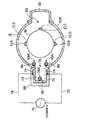
図1は本発明の係る成膜装置の実施例を示す縦断面構成図、図2は成膜装置(加熱手段は省略)を示す横断面構成図、図3は分散ノズルの上部の状態の一例を示す部分拡大図である。尚、ここでは原料ガスとしてシリコン含有ガスであるジクロロシラン(DCS)を用い、反応ガスとして窒化ガスであるアンモニアガス(NH3 )を用い、パージガスとしてN2 ガスを用い、上記NH3 ガスをプラズマにより活性化して薄膜としてシリコン窒化膜を成膜する場合を例にとって説明する。Hereinafter, an embodiment of a film forming apparatus according to the present invention will be described in detail with reference to the accompanying drawings.
FIG. 1 is a longitudinal sectional view showing an embodiment of a film forming apparatus according to the present invention, FIG. 2 is a transverse sectional view showing a film forming apparatus (heating means is omitted), and FIG. 3 is an example of a state of an upper portion of a dispersion nozzle. FIG. In this case, dichlorosilane (DCS), which is a silicon-containing gas, is used as a source gas, ammonia gas (NH3 ), which is a nitriding gas, is used as a reactive gas, N2 gas is used as a purge gas, and the NH3 gas is plasma. A case where a silicon nitride film is formed as a thin film by being activated by the above will be described as an example.
図示するように、プラズマを形成することができるこの成膜装置2は、下端が開口された有天井の円筒体状の処理容器4を有している。この処理容器4の全体は、例えば石英により形成されており、この処理容器4内の天井には、石英製の天井板6が設けられて封止されている。また、この処理容器4の下端開口部には、例えばステンレススチールにより円筒体状に成形されたマニホールド8がOリング等のシール部材10を介して連結されている。尚、ステンレス製のマニホールド8を設けないで、全体を円筒体状の石英製の処理容器で構成した装置もある。 As shown in the figure, this film forming apparatus 2 capable of forming plasma has a
上記処理容器4の下端は、上記マニホールド8によって支持されており、このマニホールド8の下方より複数枚の被処理体としての半導体ウエハWを多段に載置した保持手段としての石英製のウエハボート12が昇降可能に挿脱自在になされている。本実施例の場合において、このウエハボート12は、天板13Aと底板13Bとの間を複数本、例えば3本の支柱12Aで接続し、この支柱12Aの内側に所定のピッチで支持溝12B(図3参照)を形成して構成されており、この支持溝12BにウエハWの周辺部を支持させるようになっている。 The lower end of the
ここでは、例えば50〜150枚程度の直径が300mmのウエハWを略等ピッチで多段に支持できるようになっている。また、このウエハボート12の上端部及び下端部には、モニター用のダミー被処理体、すなわちダミーウエハDWが複数枚、図示例ではそれぞれ2枚支持されている。このダミーウエハDWの数は特に限定されない。そして、上記ダミーウエハDW及び製品用のウエハWを支持する部分が被処理体保持領域15として形成されている(図3参照)。 Here, for example, about 50 to 150 wafers having a diameter of 300 mm can be supported in multiple stages at substantially equal pitches. Further, a plurality of dummy processing objects for monitoring, that is, two dummy wafers DW, each two in the illustrated example, are supported on the upper end and lower end of the
このウエハボート12は、石英製の保温筒14を介してテーブル16上に載置されており、このテーブル16は、マニホールド8の下端開口部を開閉する例えばステンレススチール製の蓋部18を貫通する回転軸20の上端に支持される。そして、この回転軸20の貫通部には、例えば磁性流体シール22が介設され、この回転軸20を気密にシールしつつ回転可能に支持している。また、蓋部18の周辺部とマニホールド8の下端部には、例えばOリング等よりなるシール部材24が介設されており、処理容器4内のシール性を保持している。 The
上記した回転軸20は、例えばボートエレベータ等の昇降機構(図示せず)に支持されたアーム26の先端に取り付けられており、ウエハボート12及び蓋部18等を一体的に昇降して処理容器4内へ挿脱できるようになされている。尚、上記テーブル16を上記蓋部18側へ固定して設け、ウエハボート12を回転させることなくウエハWの処理を行うようにしてもよい。 The rotating
このマニホールド8には、処理容器4内に反応ガスとして例えば窒化ガスであるアンモニア(NH3 )ガスを供給する反応ガス供給手段28と、原料ガスとして例えばシリコン含有ガスであるDCS(ジクロロシラン)ガスを供給する原料ガス供給手段30と、パージガスとして不活性ガス、例えばN2 ガスを供給するパージガス供給手段34とが設けられる。The
具体的には、上記反応ガス供給手段28は、上記マニホールド8の側壁を内側へ貫通して上方向へ屈曲されて延びる石英管よりなる分散ノズル38を有している。この分散ノズル38には、その長さ方向に沿って複数(多数)のガス噴射孔38Aが所定のピッチで形成されており、各ガス噴射孔38Aから水平方向に向けて略均一にアンモニアガスを噴射できるようになっている。 Specifically, the reaction gas supply means 28 has a
また同様に上記原料ガス供給手段30も、上記マニホールド8の側壁を内側へ貫通して上方向へ屈曲されて延びる石英管よりなる分散ノズル40を有している。この分散ノズル40には、その長さ方向に沿って複数(多数)のガス噴射孔40Aが所定のピッチで形成されており、各ガス噴射孔40Aから水平方向に向けて略均一に原料ガスであるDCSガスを噴射できるようになっている。 Similarly, the source gas supply means 30 also has a
また同様にパージガス供給手段34も、上記マニホールド8の側壁を内側へ貫通して上方向へ屈曲されて延びる石英管よりなる分散ノズル44を有している。この分散ノズル44には、上記原料ガスの分散ノズル40と同様にその長さ方向に沿って複数(多数)のガス噴射孔44A(図2参照)が所定のピッチで形成されており、各ガス噴射孔44Aから水平方向に向けて略均一にN2 ガスを噴射できるようになっている。Similarly, the purge gas supply means 34 also has a
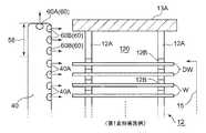
そして、上記各ガス噴射孔38A、40A、44Aは、ウエハボート12に保持された各ウエハWに対応させて略同一の水平レベルに位置するように設けられている。ここで、本実施例においては、上記各分散ノズル38、40の内の少なくともいずれか一方の分散ノズルであって上記保持手段であるウエハボート12の被処理体保持領域15よりも上方に位置するノズル上部にパーティクル放出孔を設けるようにしている。ここでは上記各分散ノズル38、40に加え、パージガス用の分散ノズル44も上記パーティクル放出孔が形成されている。尚、上記パーティクル放出孔は、少なくとも原料ガス用の分散ノズル40に設けるのが好ましい。上記3本の分散ノズル38、40、44の上端部はそれぞれ同様に構成されているので、ここでは原料ガス用の分散ノズル40を例にとって説明する。 The gas injection holes 38 </ b> A, 40 </ b> A, 44 </ b> A are provided so as to be positioned at substantially the same horizontal level corresponding to the wafers W held on the
すなわち、図3にも示すように、この原料ガス用の分散ノズル40であってウエハボート12の被処理体保持領域15よりも上方に位置するノズル上部58には、パーティクル放出孔60が形成されている。ここでは、石英製の分散ノズル40の長さは従来の分散ノズルよりもその長さが少し長く形成されてウエハボート12の天板13Aよりも上方へ延びる延長部58Aを有しており、この延長部58Aが上記ノズル上部58に含まれている。 That is, as shown in FIG. 3, the
そして、上記パーティクル放出孔60としては、分散ノズル40の上端に1つの上端側のパーティクル放出孔60Aが形成されていると共に、ノズル上部58の側壁、すなわち延長部58Aの側壁に複数、ここでは3つの側壁側のパーティクル放出孔60Bが上下方向に並べて形成されている。これらのパーティクル放出孔60の数は特に限定されない。上記上端側のパーティクル放出孔60Aからは上方に向けてガスが噴射され、側壁側のパーティクル放出孔60Bからは水平方向に向けて、すなわちウエハボート12の中心軸方向に向けてガス噴射されることになり、そのガス噴射方向にはウエハW(ダミー被処理体DWを含む)が保持されていない状態となっている。 As the
従って、被処理体保持領域15内の最上段に位置するガス噴射孔40Aと側壁側のパーティクル放出孔60Bとの間には、ガス噴射孔40Aのピッチよりも長くなされた所定の長さの盲部分62(孔がない部分)が形成されており、パーティクル放出孔60Bより放出されたパーティクルが被処理体保持領域15側へは接近しないようになっている。 Therefore, a blind of a predetermined length that is longer than the pitch of the
ここで、分散ノズル40の内径は、ガス種にもよって異なるが例えば8〜14mm程度であり、パーティクル放出孔60及びガス噴射孔40Aの直径は例えば0.8〜2.0mm程度であり、ガス噴射孔40Aのピッチは例えば8〜10mm程度である。前述したように、ノズル上部58にパーティクル放出孔60を形成した分散ノズル構造は、原料ガス用の分散ノズル40にみならず、反応ガス用の分散ノズル38及びパージガス用の分散ノズル44に対してもそれぞれ同様に形成されており、ウエハWに対するパーティクルの付着を防止するようになっている。尚、ここでは上端側のパーティクル放出孔60Aと側壁側のパーティクル放出孔60Bの双方を設けたが、これに限定されず、いずれか一方のみ設けるようにしてもよい。 Here, although the inner diameter of the
図1に戻って、上記各ノズル38、40、44には、それぞれのガス通路48、50、54が接続されている。そして、各ガス通路48、50、54には、それぞれマスフローコントローラのような流量制御器48A、50A、54A及び開閉弁48B、50B、54Bが介設されており、NH3 ガス、DCSガス及びN2 ガスをそれぞれ流量制御しつつ供給できるようになっている。Returning to FIG. 1, the
また、上記原料ガスのガス通路50の途中であって、上記流量制御器50Aと開閉弁50Bとの間には、原料ガスを一時的に貯留するバッファタンク56が介設されており、このバッファタンク56の下流側に上記開閉弁50Bを設け、上流側に開閉弁56Bを設けている。従って、上流側の開閉弁56Bを開くことにより原料ガスをバッファタンク56内へ貯留できるようになっており、下流側の開閉弁50Bを開くことによりバッファタンク56内に貯留されている原料ガスを下流側へ放出できるようになっている。 A
このバッファタンク56の容量(体積)は装置全体の大きさにもよるが、例えば1〜2リットル程度である。尚、原料ガス供給手段30のガス通路50には、バッファタンク56、流量制御器50A、開閉弁50B、56Bを含めてテープヒータ等の加熱ヒータ(図示せず)が設けられており、加熱して流れる原料ガスが液化するのを防止している。 The capacity (volume) of the
そして、上記パージガス用のガス通路54と上記反応ガス及び原料ガス用の各ガス通路48、50との間には、それぞれ途中に開閉弁48C、50Cが介設されたパージガス分岐通路55が接続されており、原料ガスや反応ガスを供給しない間欠期間に容器内雰囲気の逆流防止のためにパージガスを各分散ノズル38、40から噴射するようになっている。 A purge
一方、上記処理容器4の側壁の一部には、その高さ方向に沿ってプラズマを発生させて窒化ガスであるNH3 ガスを活性化させる活性化手段66が形成されると共に、この活性化手段66に対向する処理容器4の反対側には、この内部雰囲気を真空排気するために処理容器4の側壁を、例えば上下方向へ削りとることによって形成した細長い排気口68が設けられている。具体的には、上記活性化手段66は、上記処理容器4の側壁を上下方向に沿って所定の幅で削りとることによって上下に細長い開口70を形成し、この開口70をその外側より覆うようにして断面凹部状になされた上下に細長い例えば石英製のプラズマ区画壁72を容器外壁に気密に溶接接合することにより形成されている。On the other hand, an activation means 66 for activating NH3 gas, which is a nitriding gas, is formed on a part of the side wall of the
これにより、この処理容器4の側壁の一部を凹部状に外側へ窪ませることにより一側が処理容器4内へ開口されて連通されたプラズマ室73が形成されることになる。すなわちプラズマ区画壁72の内部空間は、上記処理容器4内に一体的に連通された状態となっている。上記開口70は、ウエハボート12の長さよりも上下方向に十分に長く形成されている。尚、この開口70に、処理容器4内とプラズマ室73とを連通する多数のスリットを有するスリット板を設ける場合もある。 Thus, a part of the side wall of the
そして、上記プラズマ区画壁72の両側壁の外側面には、その長さ方向(上下方向)に沿って互いに対向するようにして細長い一対のプラズマ電極74が設けられると共に、このプラズマ電極74にはプラズマ発生用の高周波電源76が給電ライン78を介して接続されており、上記プラズマ電極74に例えば13.56MHzの高周波電圧を印加することによりプラズマを発生し得るようになっている。尚、この高周波電圧の周波数は13.56MHzに限定されず、他の周波数、例えば400kHz等を用いてもよい。 A pair of
そして、上記処理容器4内を上方向に延びて行く反応ガス用の分散ノズル38は途中で処理容器4の半径方向外方へ屈曲されて、上記プラズマ室73内の一番奥(処理容器4の中心より一番離れた部分)に位置され、この一番奥の部分に沿って上方に向けて起立させて設けられている。従って、高周波電源76がオンされている時に上記分散ノズル38のガス噴射孔38Aから噴射されたアンモニアガスはここで活性化されて処理容器4の中心に向けて拡散しつつ流れるようになっている。 Then, the reaction
そして上記プラズマ区画壁72の外側には、これを覆うようにして例えば石英よりなる絶縁保護カバー80が取り付けられている。また、この絶縁保護カバー80の内側部分には、図示しない冷媒通路が設けられており、冷却された窒素ガスや冷却水を流すことにより上記プラズマ電極74を冷却し得るようになっている。 An insulating
そして上記プラズマ室73の開口70の外側近傍、すなわち開口70の外側(処理容器4内)には、上記原料ガス用の分散ノズル40とパージガス用の分散ノズル44とがそれぞれ起立させて設けられており、各ノズル40、44に設けた各ガス噴射孔40A、44Aより処理容器4の中心方向に向けて原料ガスであるDCSガスとパージガスであるN2 ガスとをそれぞれ噴射し得るようになっている。In the vicinity of the outside of the
一方、上記開口70に対向させて設けた排気口68には、これを覆うようにして石英よりなる断面コ字状に成形された排気口カバー部材82が溶接により取り付けられている。この排気口カバー部材82は、上記処理容器4の側壁に沿って上方に延びており、処理容器4の上方のガス出口84に連通されている。そして、このガス出口84には、排気系86が接続されている。この排気系86は、上記ガス出口84に接続される排気通路88を有しており、この排気通路88には、処理容器4内の圧力を調整する圧力調整弁90、真空ポンプ92及び排気ガス中の有害成分を除去する除去装置93が順次介設されて、処理容器4内を所定の圧力に維持しつつ真空引きできるようになっている。 On the other hand, an exhaust
上記除害装置93としては、排気ガス中の除去すべきガス成分に対応させて乾式、燃焼式或いは湿式のいずれの除害装置を用いてもよい。そして、この処理容器4の外周を囲むようにしてこの処理容器4及びこの内部のウエハWを加熱する筒体状の加熱手段94が設けられている。 As the
そして、このように構成された成膜装置2の全体の動作、例えばプロセス圧力、プロセス温度、各開閉弁の開閉によるガスの供給、供給停止、バッファタンク56への原料ガスの貯留(チャージ)、ガス流量の制御及び後述する高周波のオン・オフ制御等は例えばコンピュータ等よりなる装置制御部96により行われる。そして、この装置制御部96は、上記制御を行うためのプログラムが記憶されている記憶媒体98を有している。この記憶媒体98としては、例えばフレキシブルディスク、CD(Compact Disc)、CD−ROM、ハードディスク、フラッシュメモリ或いはDVD等を用いることができる。 Then, the overall operation of the film forming apparatus 2 configured as described above, for example, process pressure, process temperature, gas supply by opening / closing each open / close valve, supply stop, storage of source gas to the buffer tank 56 (charge), Control of the gas flow rate and high-frequency on / off control, which will be described later, are performed by an
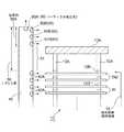
次に、以上のように構成された成膜装置2を用いて行なわれる成膜方法(いわゆるALD成膜)について図4も参照して説明する。図4は本発明の成膜装置を用いて行なわれる成膜方法における各ガスの供給態様の一例を示すタイミングチャートである。 Next, a film forming method (so-called ALD film forming) performed using the film forming apparatus 2 configured as described above will be described with reference to FIG. FIG. 4 is a timing chart showing an example of each gas supply mode in the film forming method performed using the film forming apparatus of the present invention.
この成膜方法は、上記処理容器4内へ原料ガス(DCSガス)を供給して上記原料ガスを上記被処理体である半導体ウエハWの表面に吸着させる吸着工程と、上記処理容器4内へ反応ガス(NH3 )を供給して上記被処理体の表面に吸着している上記原料ガスと反応させて上記薄膜(シリコン窒化膜)を形成する反応工程とを交互に複数回繰り返し行うようにしたものである。This film forming method includes an adsorption step of supplying a raw material gas (DCS gas) into the
まず、常温の多数枚、例えば50〜150枚の300mmサイズのウエハWが載置された状態のウエハボート12を予め所定の温度になされた処理容器4内にその下方より上昇させてロードし、蓋部18でマニホールド8の下端開口部を閉じることにより処理容器4内を密閉する。 First, the
そして処理容器4内を真空引きして所定のプロセス圧力に維持すると共に、加熱手段94への供給電力を増大させることにより、ウエハ温度を上昇させてプロセス温度を維持する。そして、上記DCSガスは原料ガス供給手段30から供給し、NH3 ガスは反応ガス供給手段28から供給し、パージガスであるN2 ガスはパージガス供給手段34から供給する。Then, the inside of the
具体的には、まず図4(A)に示すように、吸着工程においては、処理容器4内へ上記DCSガスを供給してDCSガスをウエハWの表面に吸着させる。また、これに続く反応工程においては、図4(B)に示すように上記吸着工程の後に、間欠期間102を挟んでNH3 ガスは1回パルス状に供給され、これにより、このNH3 ガスが先にウエハWの表面に吸着しているDCSガスと反応し、ここでは窒化して薄膜としてシリコン窒化膜が形成される。Specifically, as shown in FIG. 4A, first, in the adsorption step, the DCS gas is supplied into the
そして、更に、次のサイクルでは、上記反応工程の後に間欠期間104を挟んで再度、上記したような吸着工程が行われ、以下同様に上記吸着工程と反応工程とが順次繰り返されて行く。ここで、ある吸着工程の先頭と次の吸着工程の先頭との間が1サイクルとなる。そして、上記NH3 ガスを供給する時には、図4(C)に示すように高周波電源(RF)をオンにしてプラズマ室73内にプラズマを立て、この時に分散ノズル38のガス噴射孔38Aから供給されるNH3 ガスを上記プラズマにより活性化させる。Further, in the next cycle, the adsorption process as described above is performed again after the reaction process with the
このアンモニアの活性種(活性化された窒化ガス)が、上述のように先にウエハWの表面に吸着していたDCSガスを窒化し、ここに原子レベル或いは分子レベルの非常に薄いシリコン窒化膜(SiN)を形成することになる。尚、バッファタンク56内へは、例えば反応工程の時にDCSガスの貯留(チャージ)が行われている。 This active species of ammonia (activated nitriding gas) nitrifies the DCS gas previously adsorbed on the surface of the wafer W as described above, and a very thin silicon nitride film at the atomic level or molecular level here. (SiN) will be formed. For example, DCS gas is stored (charged) in the
また、ここでは処理の開始からパージガスであるN2 ガスは連続的に供給されており、各ガスの流れを促進させ、間欠期間では処理容器4内に残留している残留ガスの排出を促進させるようにしている。このパージガスは上述のように流してもよいし、或いは流さないようにしてもよい。また、原料ガスを流さない間欠期間には、原料ガス用の分散ノズル40からN2 ガスが流され、反応ガスを流さない間欠期間には反応ガス用の分散ノズル38からN2 ガスを流して処理容器4内の雰囲気が分散ノズル40、38内へ逆流することを防止している。Further, here, the N2 gas that is the purge gas is continuously supplied from the start of the process, and the flow of each gas is promoted, and the discharge of the residual gas remaining in the
上述のように、成膜処理が開始すると、排気系86が駆動して真空ポンプ92は連続的に回転駆動されて処理容器4内の雰囲気を真空引きしている。そして、上記処理容器4内で反応によって発生した反応副生成物や未反応のガス成分は排気ガスと共に排気系86内を流れて排出される。この際、上記排気ガス中に含まれる有害成分は、除害装置93にて除去されるようになっている。 As described above, when the film forming process is started, the
ここで、上記成膜処理におけるプロセス条件について説明すると、プロセス温度は450〜650℃程度、プロセス圧力は0.133〜1330Paの範囲内で変化させ、吸着工程の時には上記圧力範囲内でプロセス圧力が高くなるように設定されている。また、吸着工程におけるDCSガスの1回の供給期間T1は3sec程度、吸着工程と反応工程との間の間欠期間T3、T5は、それぞれ11secと3sec程度であり、反応工程におけるNH3 ガスの供給期間T4は20sec程度である。Here, the process conditions in the film forming process will be described. The process temperature is changed in the range of about 450 to 650 ° C., the process pressure is changed in the range of 0.133 to 1330 Pa, and the process pressure is within the pressure range in the adsorption step. It is set to be high. In addition, the one supply period T1 of DCS gas in the adsorption process is about 3 sec, and the intermittent periods T3 and T5 between the adsorption process and the reaction process are about 11 sec and 3 sec, respectively. The supply of NH3 gas in the reaction process The period T4 is about 20 seconds.
またDCSガスの流量は1〜2slm程度、NH3 ガスの流量は1〜10slm程度、パージガスであるN2 ガスの流量は0.1〜1.0slm程度である。The flow rate of DCS gas is about 1 to2 slm, the flow rate of NH3 gas is about 1 to 10 slm, and the flow rate of N2 gas that is a purge gas is about 0.1 to 1.0 slm.
さて、上述のように原料ガスであるDCSガスと反応ガスであるNH3 ガスとをそれぞれ分散ノズル40、38から間欠的に供給していると、前述したように間欠期間中は各分散ノズル40、38からパージガスを流すようにしているとはいえ、処理容器4内の雰囲気が各分散ノズル40、38内へ逆拡散してくることは避けられない。この結果、分散ノズル40、38内の壁面にシリコン窒化膜が形成され、このシリコン窒化膜自体の高いストレス(応力)により石英製の分散ノズル40、38にクラック(チッピング)が生じて微小なパーティクルが発生する傾向となる。As described above, when the DCS gas that is the source gas and the NH3 gas that is the reaction gas are intermittently supplied from the
このパーティクル発生の傾向は、処理容器4内に配置されている原料ガス用の分散ノズル40において顕著となる。また高い圧力で供給されるDCSガスの供給途中においても原料ガスの一部が反応してシリコン窒化膜等のシリコン副生成物がパーティクルとなって流れてくる。これらのパーティクルは分散ノズル40、38の先端部に滞留し易くなっている。そして、このようなパーティクルは、分散ノズル40、38の各ガス噴射孔40A、38Aからガスと共に処理容器4内へ放出されてウエハWに付着する危惧が生ずることになる。 This tendency of particle generation becomes remarkable in the
しかしながら、本実施例においては、各分散ノズル40、38のノズル上部58(図3参照)にパーティクル放出孔60(60A、60B)を設けているので、パーティクル放出孔60(60A、60B)からガスが放出される分だけ分散ノズル40、38内の圧力が低下し、また原料ガスや反応ガスに随伴されてきた大部分のパーティクルは上記パーティクル放出孔60から処理容器4内側へ噴射されることになる。このパーティクル放出孔60が形成されている部分及びこのパーティクル放出孔60からのガス噴射方向には半導体ウエハW(ダミー被処理体DWを含む)が保持されていないので、処理容器4内へ放出されたパーティクルはウエハ表面に付着することなく、そのまま反対側に位置する排気口68より処理容器4の外へ排出されることになる。 However, in this embodiment, since the particle discharge holes 60 (60A, 60B) are provided in the nozzle upper portions 58 (see FIG. 3) of the
本実施例の場合には、特に、各分散ノズル40、38の長さを長くしてウエハボート12の天板13Aよりも上方に位置する延長部58Aに上記各パーティクル放出孔60A、60Bを設けるようにして、パーティクル放出孔60A、60Bの形成位置をウエハW(ダミー被処理体DWを含む)からより遠く離れた場所に設定しているので、パーティクル付着抑制効果を一層高めることができる。 In the case of the present embodiment, the
上述したようなパーティクル付着抑制効果は、原料ガス用の分散ノズル40において特に顕著に発揮されるが、同じような構造になされた他の分散ノズル38、44においても同様に発揮されることになる。 The effect of suppressing the adhesion of particles as described above is particularly noticeable in the
<パーティクル分布量のシミュレーション>
ここで多数のガス噴射孔を有する分散ノズルから放出されるパーティクルの分布量についてシミュレーションを行ったので、そのシミュレーション結果について説明する。図5は多数のガス噴射孔を有する分散ノズルから放出されるパーティクルの分布量を示すグラフである。分散ノズル110には多数、例えば100〜150個程度のガス噴射孔112が7〜10mmのピッチの間隔で形成されている。この分散ノズル110に原料ガス(DCSガス)を100〜150Torr程度の圧力範囲内で供給し、各ガス噴射孔112からガスを放出している。分散ノズル110の内径は8〜14mm、ガス噴射孔112の直径は0.8〜2.0mmである。パーティクル分布量のグラフから明らかなように、ガス流の最下流である分散ノズル110の上端部に設けたガス噴射孔112A(112)からのパーティクル量が、他の部分に形成したガス噴射孔112から排出されるパーティクル量よりも遥かに多いことが判る。<Simulation of particle distribution>
Here, since the simulation was performed on the distribution amount of the particles emitted from the dispersion nozzle having a large number of gas injection holes, the simulation result will be described. FIG. 5 is a graph showing the distribution amount of particles emitted from a dispersion nozzle having a large number of gas injection holes. A large number, for example, about 100 to 150 gas injection holes 112 are formed in the
従って、本発明のように、分散ノズル38、40であって、ウエハボート12の被処理体保持領域15よりも上方に位置するノズル上部58にパーティクル放出孔60を設けているので、このパーティクル放出孔60から大部分のパーティクルを放出させることができ、これによりウエハ表面にパーティクルが付着することを阻止できることが判る。 Accordingly, as in the present invention, since the particle discharge holes 60 are provided in the nozzle
このように、原料ガスと反応ガスを処理容器4内へ供給する分散ノズル38、40の内の少なくともいずれか一方の分散ノズルであって、保持手段12の被処理体保持領域15よりも上方に位置するノズル上部58にパーティクル放出孔60を設けて、分散ノズル内等で発生したパーティクルをこのパーティクル放出孔60より主に排出させるようにしたので、被処理体保持領域15に支持されている被処理体Wにパーティクルが付着することを大幅に抑制することができる。 In this way, at least one of the
<実験結果>
ここで上記した成膜装置を用いて実際にシリコン窒化膜の成膜処理を行った時のパーティクルについて測定したので、その測定結果について説明する。従来の成膜装置のウエハボートの最上段の近傍の半導体ウエハのパーティクル数は、0.1μm以上のものが100個程度であったが、原料ガス用の分散ノズル40に図3に示すようなパーティクル放出孔60を設けた本発明の成膜装置の場合には、パーティクル数は0.1μm以上のものが10個程度であり、パーティクルを大幅に減少させることができることを確認することができた。<Experimental result>
Here, since particles were measured when the silicon nitride film was actually formed using the film forming apparatus described above, the measurement results will be described. The number of particles of the semiconductor wafer in the vicinity of the uppermost stage of the wafer boat of the conventional film forming apparatus was about 100 having a particle size of 0.1 μm or more. However, as shown in FIG. In the case of the film forming apparatus of the present invention provided with the particle discharge holes 60, the number of particles is about 10 having a particle size of 0.1 μm or more, and it was confirmed that the particles can be greatly reduced. .
<第1変形実施例>
次に、本発明の第1変形実施例について説明する。先の実施例にあっては、分散ノズル38、40、44の長さを通常よりも長くしてノズル上部58に延長部58Aを設け、この延長部58Aにパーティクル放出孔60を形成したが、これに限定されず、分散ノズル38、40、44の長さを延ばすことなく通常の長さに設定した状態で、ノズル上部58にパーティクル放出孔60を形成するようにしてもよい。図6はこのような分散ノズルの第1変形実施例を示す部分拡大図である。図6中において図1乃至図3に示した構成と同一構成部分については同一参照符号を付してその説明を省略する。ここでも原料ガス用の分散ノズル40を例にとって説明するが、この第1変形実施例を他の分散ノズル38、44にも適用できるのは勿論である。<First Modification>
Next, a first modified embodiment of the present invention will be described. In the previous embodiment, the length of the
図6に示すように、ここでは分散ノズル40の長さは従来の成膜装置の場合と同様であり、その先端はウエハボート12の天板13Aと略同一の水平レベルになされている。そして、この分散ノズル40であって、上記ウエハボート12の被処理体保持領域15よりも上方に位置するノズル上部58にパーティクル放出孔60を形成している。図示例でも図3の場合と同様に、上端側のパーティクル放出孔60Aと側壁側のパーティクル放出孔60Bの双方を設けた場合について記載しているが、上記パーティクル放出孔60A、60B内のいずれか一方のみを設けるようにしてもよいし、これらの孔数は特に限定されないのも図3において説明した場合と同じである。 As shown in FIG. 6, here, the length of the
また、ここでは3個の側壁側のパーティクル放出孔60Bは、その下方に形成されている通常のガス噴射孔40Aに連続してこれらと同じピッチの間隔で形成されているが、この3個のパーティクル放出孔60Bの内の最下部の1つ或いは2つのパーティクル放出孔60Bを設けないようにして、この部分を盲部分62(図3参照)としてもよい。 In addition, here, the three side wall side particle discharge holes 60B are formed at regular intervals of the same pitch as the normal
この第1変形実施例の場合には、パーティクル放出孔60Bより噴射されたガスは、天板13Aと最上段のダミー被処理体DWとの間の空間部120を水平方向に流れることになり、このガスに含まれるパーティクルはダミー被処理体DWやウエハWの表面に付着することが抑制される。そして、各パーティクル放出孔60は、図3に示す実施例よりも盲部分62がなくなった分だけガス噴射孔40Aに接近した状態で形成されることになるため、ウエハWに対するパーティクル付着抑制効果は少し劣化するが、それでも、図3に示す場合と同様にパーティクル付着抑制効果を十分に発揮することができる。 In the case of this first modified embodiment, the gas injected from the
<第2変形実施例>
次に本発明の第2変形実施例について説明する。先の各実施例では側壁側のパーティクル放出孔60のガス噴射方向は、ウエハボート12の中心軸方向に向けられていたが、これに限定されず、中心軸方向よりも外側へそれた方向に向けるようにしてもよい。図7はこのような分散ノズルの第2変形実施例を示す部分拡大図であり、図7(A)は側断面図、図7(B)は平面図である。図7中において図1乃至図3及び図6に示した構成と同一構成部分については同一参照符号を付してその説明を省略する。ここでも原料ガス用の分散ノズル40を例にとって説明するが、この第2変形実施例を他の分散ノズル38、44にも適用できるのは勿論である。<Second Modification>
Next, a second modified embodiment of the present invention will be described. In each of the previous embodiments, the gas injection direction of the
図7に示すように、ここでも図6に示す場合と同様に分散ノズル40の長さは従来の成膜装置の場合と同様であり、その先端はウエハボート12の天板13Aと略同一の水平レベルになされている。そして、この分散ノズル40であって、上記ウエハボート12の被処理体保持領域15よりも上方に位置するノズル上部58にパーティクル放出孔60を形成している。 As shown in FIG. 7, the length of the
この場合、このパーティクル放出孔60として、2つの側壁側のパーティクル放出孔60Bが横方向に並んで設けられており、そのガス噴射方向がウエハボート12の中心軸C1の方向、すなわちウエハW(ダミー被処理体DWを含む)の中心軸方向よりも外側へそれた方向に向けられている。ここでは、ウエハWの上方向への投影輪郭に対する接線方向よりも外側へそれた方向に向けられている。これによりパーティクル放出孔60Bから原料ガスと共に噴射されるパーティクルがウエハWの表面に付着することを抑制することができる。 In this case, two
またこのパーティクル放出孔60Bと最上段のガス噴射孔40Aとの間には孔が形成されていない盲部分62が設けられている。上記パーティクル放出孔60Bのガス噴射方向は、好ましくは上述のようにウエハWの上方向への投影輪郭に対する接線方向よりも外側へそれた方向に向けるのが好ましい。また、このパーティクル放出孔60BをウエハWの中心軸C1の方向とは反対側、すなわちガス噴射孔40Aの形成位置とは反対側の背面(裏面)に形成するようにしてもよい。 Further, a
また、このウエハボート12の中心軸方向よりも外側へそれたガス噴射孔を有するパーティクル放出孔60Bの数は、1個又は2個以上設けることができ、複数のパーティクル放出孔60Bを図7(B)に示すように横方向に並設してもよく、或いは上下方向において位置ずれさせて設けるようにしてもよい。この第2変形実施例の場合にも、先の各実施例と同様なウエハWに対するパーティクル付着抑制効果を発揮することができる。そして、この図7に示す第2変形実施例と図6に示す第1変形実施例とを組み合わせるようにしてもよい。 In addition, the number of the particle discharge holes 60B having the gas injection holes deviating outward from the central axis direction of the
尚、以上の説明では、原料ガス用、反応ガス用及びパージガス用の各分散ノズルについてパーティクル放出孔60を設ける場合について説明したが、これに限定されず、薄膜中にドープされる不純物を含む不純物ガスを導入する不純物ガス供給手段を設ける場合もあり、このような場合には、この不純物ガス供給手段の分散ノズルに対しても、先に説明した各実施例を適用することができる。上記不純物としては、例えばボロン、炭素等が挙げられる。 In the above description, the case where the particle discharge holes 60 are provided for the dispersion nozzles for the source gas, the reaction gas, and the purge gas has been described. However, the present invention is not limited to this, and impurities including impurities doped in the thin film In some cases, an impurity gas supply means for introducing gas may be provided. In such a case, the embodiments described above can be applied to the dispersion nozzle of the impurity gas supply means. Examples of the impurities include boron and carbon.
また、ここでは薄膜としてシリコン窒化膜を成膜する場合を例にとって説明したが、これに限定されず、シリコン窒化膜(SiON)や不純物、例えばボロン等を含むシリコン窒化膜等を成膜する場合にも本発明を適用することができる。 Although the case where a silicon nitride film is formed as a thin film has been described here as an example, the present invention is not limited to this, and a silicon nitride film (SiON) or a silicon nitride film containing impurities such as boron is formed. The present invention can also be applied to.
また、ここでは原料ガスの一例であるシリコン含有ガスとしてDCSガスを用いたが、これに限定されず、上記シリコン含有ガスは、ジクロロシラン(DCS)、ヘキサクロロジシラン(HCD)、モノシラン[SiH4 ]、ジシラン[Si2 H6 ]、ヘキサメチルジシラザン(HMDS)、テトラクロロシラン(TCS)、ジシリルアミン(DSA)、トリシリルアミン(TSA)、アミノシラン系ガスよりなる群より選択される1以上のガスを用いることができる。Moreover, although DCS gas was used here as a silicon-containing gas which is an example of the source gas, the silicon-containing gas is not limited to this, and the silicon-containing gas may be dichlorosilane (DCS), hexachlorodisilane (HCD), or monosilane [SiH4 ]. At least one gas selected from the group consisting of disilane [Si2 H6 ], hexamethyldisilazane (HMDS), tetrachlorosilane (TCS), disilylamine (DSA), trisilylamine (TSA), and aminosilane-based gas. Can be used.
また、上記アミノシラン系ガスとしては、BAS(ブチルアミノシラン)、BTBAS(ビスターシャリブチルアミノシラン)、DMAS(ジメチルアミノシラン)、BDMAS(ビスジメチルアミノシラン)、TDMAS(トリジメチルアミノシラン)、DEAS(ジエチルアミノシラン)、BDEAS(ビスジエチルアミノシラン)、DPAS(ジプロピルアミノシラン)、DIPAS(ジイソプロピルアミノシラン)よりなる群から選択される1以上のガスを用いることができる。 Examples of the aminosilane-based gas include BAS (butylaminosilane), BTBAS (bisteria butylaminosilane), DMAS (dimethylaminosilane), BDMAS (bisdimethylaminosilane), TDMAS (tridimethylaminosilane), DEAS (diethylaminosilane), and BDEAS. One or more gases selected from the group consisting of (bisdiethylaminosilane), DPAS (dipropylaminosilane), and DIPAS (diisopropylaminosilane) can be used.
更には、原料ガスとしてシリコン含有ガスに限定されず、有機金属化合物ガスを用いることができる。この有機金属化合物ガスとしては、トリメチルアルミニウム(TMA)、テトラキスジメチルアミノハフニウム(TDMAH)、テトラキスエチルメチルアミノハフニウム(TEMAH)、テトラキスエチルメチルアミノジルコニウム(TEMAZ)、テトラキスジメチルアミノチタン(TDMAT)よりなる群より選択される1以上のガス用いることができる。また、ここでは反応ガスとして窒化ガス(NH3 ガス)を用いたが、処理態様によっては、O2 等の酸化ガス、或いは水素等の還元ガスを用いることもできる。また、上記反応ガスを、窒素ガス又は酸化ガス(酸素やオゾン)等により必要に応じて活性化するようにしてもよい。Furthermore, the source gas is not limited to a silicon-containing gas, and an organometallic compound gas can be used. Examples of the organometallic compound gas include trimethylaluminum (TMA), tetrakisdimethylaminohafnium (TDMAH), tetrakisethylmethylaminohafnium (TEMAH), tetrakisethylmethylaminozirconium (TEMAZ), and tetrakisdimethylaminotitanium (TDMAT). One or more selected gases can be used. Further, although a nitriding gas (NH3 gas) is used here as a reaction gas, an oxidizing gas such as O2 or a reducing gas such as hydrogen can be used depending on the processing mode. Further, the reaction gas may be activated with nitrogen gas or oxidizing gas (oxygen or ozone) as necessary.
また、ここでは被処理体として半導体ウエハを例にとって説明したが、この半導体ウエハにはシリコン基板やGaAs、SiC、GaNなどの化合物半導体基板も含まれ、更にはこれらの基板に限定されず、液晶表示装置に用いるガラス基板やセラミック基板等にも本発明を適用することができる。 Although the semiconductor wafer is described as an example of the object to be processed here, the semiconductor wafer includes a silicon substrate and a compound semiconductor substrate such as GaAs, SiC, GaN, and the like, and is not limited to these substrates. The present invention can also be applied to glass substrates, ceramic substrates, and the like used in display devices.
2 成膜装置
4 処理容器
12 ウエハボート(保持手段)
13A 天板
13B 底板
15 被処理体保持領域
18 蓋部
28 反応ガス供給手段
30 原料ガス供給手段
34 パージガス供給手段
56 バッファタンク
58 ノズル上部
58A 延長部
60、60A、60B パーティクル放出孔
66 活性化手段
74 プラズマ電極
76 高周波電源
86 排気系
94 加熱手段
96 装置制御部
W 半導体ウエハ(被処理体)
2
Claims (13)
Translated fromJapanese真空引き可能になされた処理容器と、
天板と底板との間で複数枚の前記被処理体を前記処理容器内で保持する保持手段と、
前記被処理体を加熱する加熱手段と、
原料ガスを供給するために前記処理容器の長手方向に沿って延びると共に複数のガス噴射孔が形成された分散ノズルを有する原料ガス供給手段と、
反応ガスを供給するために前記処理容器の長手方向に沿って延びると共に複数のガス噴射孔が形成された分散ノズルを有する反応ガス供給手段と、
装置全体の動作を制御する装置制御部とを備え、
前記分散ノズルの内の少なくともいずれか一方の分散ノズルであって前記保持手段の被処理体保持領域よりも上方に位置するノズル上部は前記保持手段の天板よりも上方へ延びる延長部を有すると共に前記延長部にパーティクル放出孔を設けるように構成したことを特徴とする成膜装置。In a film forming apparatus for forming a thin film on the surface of an object to be processed,
A processing vessel that can be evacuated;
Holding means for holding a plurality of the objects to be processed in the processing container between a top plate and a bottom plate;
Heating means for heating the object to be processed;
A raw material gas supply means having a dispersion nozzle that extends along the longitudinal direction of the processing vessel and has a plurality of gas injection holes formed to supply the raw material gas;
Reactive gas supply means having a dispersion nozzle extending along the longitudinal direction of the processing vessel and supplying a plurality of gas injection holes to supply the reactive gas;
A device control unit for controlling the operation of the entire device,
The upper partof the nozzle, which is at least one of the dispersion nozzles and is located above the workpiece holding region of theholding means, has an extension extending upward from the top plate of the holding means. A film forming apparatus characterized in that a particle discharge hole is provided in theextension portion .
Priority Applications (1)
| Application Number | Priority Date | Filing Date | Title |
|---|---|---|---|
| JP2012017528AJP5887962B2 (en) | 2012-01-31 | 2012-01-31 | Deposition equipment |
Applications Claiming Priority (1)
| Application Number | Priority Date | Filing Date | Title |
|---|---|---|---|
| JP2012017528AJP5887962B2 (en) | 2012-01-31 | 2012-01-31 | Deposition equipment |
Publications (2)
| Publication Number | Publication Date |
|---|---|
| JP2013157491A JP2013157491A (en) | 2013-08-15 |
| JP5887962B2true JP5887962B2 (en) | 2016-03-16 |
Family
ID=49052388
Family Applications (1)
| Application Number | Title | Priority Date | Filing Date |
|---|---|---|---|
| JP2012017528AActiveJP5887962B2 (en) | 2012-01-31 | 2012-01-31 | Deposition equipment |
Country Status (1)
| Country | Link |
|---|---|
| JP (1) | JP5887962B2 (en) |
Families Citing this family (14)
| Publication number | Priority date | Publication date | Assignee | Title |
|---|---|---|---|---|
| JP6291297B2 (en)* | 2014-03-17 | 2018-03-14 | 東京エレクトロン株式会社 | Film forming method, film forming apparatus, and storage medium |
| JP6578243B2 (en) | 2015-07-17 | 2019-09-18 | 株式会社Kokusai Electric | Gas supply nozzle, substrate processing apparatus, semiconductor device manufacturing method and program |
| JP6560924B2 (en) | 2015-07-29 | 2019-08-14 | 株式会社Kokusai Electric | Substrate processing apparatus, semiconductor device manufacturing method, and program |
| WO2018008088A1 (en)* | 2016-07-05 | 2018-01-11 | 株式会社日立国際電気 | Substrate treatment apparatus, gas nozzle, and semiconductor device manufacturing method |
| JP2018170468A (en)* | 2017-03-30 | 2018-11-01 | 東京エレクトロン株式会社 | Vertical heat treatment apparatus |
| KR102009348B1 (en)* | 2017-09-20 | 2019-08-09 | 주식회사 유진테크 | Batch type plasma substrate processing apparatus |
| JP6952595B2 (en)* | 2017-12-20 | 2021-10-20 | 東京エレクトロン株式会社 | Vertical heat treatment equipment |
| WO2019188037A1 (en)* | 2018-03-30 | 2019-10-03 | 株式会社Kokusai Electric | Substrate treatment device, method for manufacturing semiconductor device, and program |
| KR102034766B1 (en)* | 2018-04-12 | 2019-10-22 | 주식회사 유진테크 | Apparatus for processing substrate and method for processing substrate |
| JP7012613B2 (en)* | 2018-07-13 | 2022-01-28 | 東京エレクトロン株式会社 | Film formation method and film formation equipment |
| KR102783210B1 (en)* | 2019-09-09 | 2025-03-19 | 주식회사 원익아이피에스 | Gas supply nozzle and substrate processing apparatus using the same |
| JP7365973B2 (en) | 2020-06-19 | 2023-10-20 | 東京エレクトロン株式会社 | Gas nozzle, substrate processing equipment and substrate processing method |
| JP7455013B2 (en) | 2020-07-10 | 2024-03-25 | 東京エレクトロン株式会社 | Plasma processing equipment and plasma processing method |
| KR102859401B1 (en)* | 2021-08-24 | 2025-09-12 | 주식회사 원익아이피에스 | Substrate processing apparatus |
Family Cites Families (4)
| Publication number | Priority date | Publication date | Assignee | Title |
|---|---|---|---|---|
| US20010052556A1 (en)* | 1998-12-14 | 2001-12-20 | Weichi Ting | Injector |
| JP4873820B2 (en)* | 2002-04-01 | 2012-02-08 | 株式会社エフティーエル | Semiconductor device manufacturing equipment |
| JP4935687B2 (en)* | 2008-01-19 | 2012-05-23 | 東京エレクトロン株式会社 | Film forming method and film forming apparatus |
| JP2009260151A (en)* | 2008-04-18 | 2009-11-05 | Tokyo Electron Ltd | Method of forming metal doped layer, film forming apparatus, and storage medium |
- 2012
- 2012-01-31JPJP2012017528Apatent/JP5887962B2/enactiveActive
Also Published As
| Publication number | Publication date |
|---|---|
| JP2013157491A (en) | 2013-08-15 |
Similar Documents
| Publication | Publication Date | Title |
|---|---|---|
| JP5887962B2 (en) | Deposition equipment | |
| JP5920242B2 (en) | Film forming method and film forming apparatus | |
| JP5233562B2 (en) | Film forming method and film forming apparatus | |
| JP4935687B2 (en) | Film forming method and film forming apparatus | |
| JP5190307B2 (en) | Film forming method, film forming apparatus, and storage medium | |
| JP4935684B2 (en) | Film forming method and film forming apparatus | |
| JP4179311B2 (en) | Film forming method, film forming apparatus, and storage medium | |
| JP5151260B2 (en) | Film forming method and film forming apparatus | |
| JP4506677B2 (en) | Film forming method, film forming apparatus, and storage medium | |
| JP4396547B2 (en) | Film forming method, film forming apparatus, and storage medium | |
| JP4305427B2 (en) | Film forming method, film forming apparatus, and storage medium | |
| JP4929811B2 (en) | Plasma processing equipment | |
| JP4258518B2 (en) | Film forming method, film forming apparatus, and storage medium | |
| JP4434149B2 (en) | Film forming method, film forming apparatus, and storage medium | |
| KR101503725B1 (en) | Film forming method and film forming apparatus | |
| JP4893729B2 (en) | Film forming method, film forming apparatus, and storage medium | |
| JP4929932B2 (en) | Film forming method, film forming apparatus, and storage medium | |
| JP6024484B2 (en) | Film forming method and film forming apparatus | |
| JP2009260151A (en) | Method of forming metal doped layer, film forming apparatus, and storage medium | |
| US20150031216A1 (en) | Cleaning method, method of manufacturing semiconductor device, substrate processing apparatus, and recording medium | |
| JP2008227460A (en) | Film forming method and film forming apparatus | |
| JP2011029284A (en) | Film forming method and film forming device | |
| JP2006066884A (en) | Film forming method, film forming apparatus, and storage medium | |
| JP5082595B2 (en) | Deposition equipment | |
| JP4793306B2 (en) | Plasma processing method and storage medium |
Legal Events
| Date | Code | Title | Description |
|---|---|---|---|
| A621 | Written request for application examination | Free format text:JAPANESE INTERMEDIATE CODE: A621 Effective date:20140621 | |
| A977 | Report on retrieval | Free format text:JAPANESE INTERMEDIATE CODE: A971007 Effective date:20150316 | |
| A131 | Notification of reasons for refusal | Free format text:JAPANESE INTERMEDIATE CODE: A131 Effective date:20150331 | |
| A521 | Request for written amendment filed | Free format text:JAPANESE INTERMEDIATE CODE: A523 Effective date:20150520 | |
| TRDD | Decision of grant or rejection written | ||
| A01 | Written decision to grant a patent or to grant a registration (utility model) | Free format text:JAPANESE INTERMEDIATE CODE: A01 Effective date:20160119 | |
| A61 | First payment of annual fees (during grant procedure) | Free format text:JAPANESE INTERMEDIATE CODE: A61 Effective date:20160201 | |
| R150 | Certificate of patent or registration of utility model | Ref document number:5887962 Country of ref document:JP Free format text:JAPANESE INTERMEDIATE CODE: R150 | |
| R250 | Receipt of annual fees | Free format text:JAPANESE INTERMEDIATE CODE: R250 | |
| R250 | Receipt of annual fees | Free format text:JAPANESE INTERMEDIATE CODE: R250 | |
| R250 | Receipt of annual fees | Free format text:JAPANESE INTERMEDIATE CODE: R250 | |
| R250 | Receipt of annual fees | Free format text:JAPANESE INTERMEDIATE CODE: R250 | |
| R250 | Receipt of annual fees | Free format text:JAPANESE INTERMEDIATE CODE: R250 | |
| R250 | Receipt of annual fees | Free format text:JAPANESE INTERMEDIATE CODE: R250 | |
| R250 | Receipt of annual fees | Free format text:JAPANESE INTERMEDIATE CODE: R250 |