JP5885638B2 - Semiconductor memory device - Google Patents
Semiconductor memory deviceDownload PDFInfo
- Publication number
- JP5885638B2 JP5885638B2JP2012238851AJP2012238851AJP5885638B2JP 5885638 B2JP5885638 B2JP 5885638B2JP 2012238851 AJP2012238851 AJP 2012238851AJP 2012238851 AJP2012238851 AJP 2012238851AJP 5885638 B2JP5885638 B2JP 5885638B2
- Authority
- JP
- Japan
- Prior art keywords
- flag
- data
- confidential information
- memory device
- area
- Prior art date
- Legal status (The legal status is an assumption and is not a legal conclusion. Google has not performed a legal analysis and makes no representation as to the accuracy of the status listed.)
- Active
Links
Images


Landscapes
- Read Only Memory (AREA)
- Storage Device Security (AREA)
Description
Translated fromJapanese本発明の実施形態は、半導体記憶装置に関する。 Embodiments described herein relate generally to a semiconductor memory device.
近年、NAND型フラッシュメモリを搭載したメディアなどに動画などのコンテンツを記憶させることが増えている。コンテンツの権利を守るために、そのようなメディアを動画再生機などのホスト機器が「認証する」という機能が考えられている。たとえば、ホスト機器は、メディアが正規のものか、不正にコピーされたものかを識別し、識別の結果が後者であった場合には動画の再生を拒否する。認証のために、NAND型フラッシュメモリの内部の特定の領域に、工場出荷時に認証に必要なデータ(例えば秘密鍵)を書いておく。この特定の領域のデータが不特定のユーザによって書き換えられることが可能な状態にあった場合、攻撃者はこの領域を消去して認証をパスするようなデータを書き込むことで、不正な複製メディアを作ることが可能となる。 In recent years, contents such as moving images have been increasingly stored in media equipped with a NAND flash memory. In order to protect the rights of content, a function that “authenticates” such media by a host device such as a video player is considered. For example, the host device identifies whether the medium is legitimate or illegally copied, and if the identification result is the latter, it rejects the reproduction of the moving image. For authentication, data (for example, a secret key) necessary for authentication is written in a specific area inside the NAND flash memory at the time of factory shipment. If the data in this specific area can be rewritten by an unspecified user, the attacker erases this area and writes data that passes the authentication, so that unauthorized duplication media can be stored. It becomes possible to make.
機密情報を保護可能な半導体記憶装置を提供しようとするものである。 A semiconductor storage device capable of protecting confidential information is provided.
一実施形態による半導体記憶装置は、機密情報を保持する機密情報領域を含むメモリを含む。機密情報領域は有効にされたフラグを含んでいる。制御回路は、機密情報領域に対するデータ消去を指示されると、機密情報領域中のデータをメモリから読み出し、読み出されたデータ中でフラグが有効であるかを判定し、無効である場合は機密情報領域中のデータを消去し、有効である場合はデータ消去の指示により求められる処理を中止する。メモリは、データを保持する複数のページを含んだ情報保持領域と、複数のページについての管理情報を、1ビットの情報を当該1ビットの情報が有効である場合にnビット(nは自然数)のランダムデータによって表示する管理情報領域を含む。制御回路は、管理情報領域中にランダムデータが書かれているかを判断し、書かれている場合に対応する管理情報のビットが有効であると判断する。The semiconductor memory device according to an embodimentincludes a memorycontaining sensitive information area for holding secret information. The confidential information area contains a validated flag. When the control circuit is instructed to erase data in the confidential information area, it reads out the data in the confidential information area from the memory, determines whether the flag is valid in the read data, and if it is invalid, the control circuit The data in the information area is erased, and if it is valid, the processing requested by the data erasure instruction is stopped.The memory has an information holding area including a plurality of pages for holding data, management information for the plurality of pages, 1 bit of information when the 1 bit of information is valid (n is a natural number) Management information area to be displayed by random data. The control circuit determines whether random data is written in the management information area, and determines that the management information bit corresponding to the random data is valid.
本発明者等は、実施形態の開発の過程において、以下に述べるような知見を得た。NAND型フラッシュメモリ中の機密情報の書き換えを防ぐためには、機密情報の消去のみが禁止されていればよい。なぜなら、NAND型フラッシュメモリでは、メモリセルの特性に起因して、いったん書き込まれた情報を上書きすることができないからである。すなわち、データの書き込みは、消去状態の閾値電圧を有する複数メモリセルに対してのみ可能である。 The inventors have obtained the following knowledge in the process of developing the embodiment. In order to prevent rewriting of confidential information in the NAND flash memory, it is sufficient that only erasure of confidential information is prohibited. This is because in a NAND flash memory, information once written cannot be overwritten due to the characteristics of the memory cell. In other words, data can be written only to a plurality of memory cells having a threshold voltage in the erased state.
上記のように機密情報を保持する領域の書き換えは防がれる必要がある。しかし一方で機密情報をこの領域に書き込むことが必要であり、また、機密情報が書き込まれる前に、メモリに対するデータ消去および書き込みのテストが行われる必要がある。したがって、機密情報書き込み前のテストおよび機密情報書き込みの際は機密情報保持領域中に対してデータ書き込みおよび消去が可能であって、かつ機密情報書き込み後はこの領域に対するデータ消去(ひいては書き込みも)が禁止されるようにしなければならない。 As described above, it is necessary to prevent rewriting of the area holding confidential information. However, on the other hand, it is necessary to write confidential information in this area, and before the confidential information is written, it is necessary to perform a data erasure and writing test on the memory. Therefore, in the test before writing confidential information and writing confidential information, data can be written and erased in the confidential information holding area, and after the confidential information is written, data can be erased (and thus written) in this area. It must be prohibited.
この機密情報書き込み前後の制約を最も簡単に実現する方法として、「機密情報書き込み前」と「機密情報書き込み後」とで異なる値を有するロムフューズパラメータを用意することが考えられる。ロムフューズパラメータは、メモリの種々の設定を規定するためのものである。メモリ中にはロムフューズパラメータを記憶するための特別のブロックが設けられており、最初に半導体記憶装置へ電源を供給する際にロムフューズパラメータが読み出され(パワーオンリード)、読み出された値が制御回路内部のラッチに格納される。機密情報書き込み前は、機密情報保持領域についてのパラメータがこの領域へのデータの書き込みおよび消去を許可する値に設定される。一方、機密情報書き込み後は、パラメータは、機密情報保持領域へのデータの書き込みおよび消去を禁止する値に設定される。禁止の値にセットされていると、例えばメモリは、データ書き込みおよび消去のコマンドをラッチせず、あるいは、コマンドをラッチはするが、データ書き込みおよび消去のシーケンス進入後に実際の動作を行わずにシーケンスをすぐに抜けるように構成される。 As a method of realizing the restriction before and after writing confidential information most easily, it is conceivable to prepare ROM fuse parameters having different values for “before writing confidential information” and “after writing confidential information”. The ROM fuse parameter is for defining various settings of the memory. A special block for storing the ROM fuse parameters is provided in the memory. When the power is first supplied to the semiconductor memory device, the ROM fuse parameters are read (power-on read) and the read values are read. Is stored in a latch inside the control circuit. Before the confidential information is written, the parameter for the confidential information holding area is set to a value that permits writing and erasing of data in this area. On the other hand, after the confidential information is written, the parameter is set to a value that prohibits writing and erasing of data in the confidential information holding area. When set to a prohibited value, for example, the memory does not latch data write and erase commands, or latches commands but does not perform actual operations after entering the data write and erase sequences. It is configured to exit immediately.
しかしながら、ロムフューズパラメータは、メモリの工場出荷後も書き換えが可能になっている。外部から専用の書き換えコマンドとパラメータのアドレスを入力すれば、パラメータを保持する領域にアクセスして値を書き換えることができるし、外部に読み出すこともできる。この機能は、本来テストモードのためのものであったが、近年ではユーザにも一部公開されている。したがって、攻撃者がロムフューズパラメータにアクセスして値を書き換えることを試みれば(たとえば全てのパラメータの値を反転させる)、機密情報の保持領域に対する消去動作のロックを外すことも可能である。ロムフューズパラメータによる機密情報の保護に対しては、こうした問題が残る。 However, the ROM fuse parameter can be rewritten even after the memory is shipped from the factory. If a dedicated rewrite command and parameter address are input from the outside, the value can be rewritten by accessing the area holding the parameter, and can be read out to the outside. This function was originally intended for the test mode, but in recent years it has been partially released to users. Therefore, if an attacker tries to rewrite the value by accessing the ROM fuse parameter (for example, inverting the values of all parameters), it is possible to unlock the erasure operation for the confidential information holding area. These problems remain for the protection of confidential information by the Romfuse parameter.
以下に、このような知見に基づいて構成された実施形態について図面を参照して説明する。以下の説明において、略同一の機能及び構成を有する構成要素については、同一符号を付し、重複説明は必要な場合にのみ行う。また、各実施形態は、この実施形態の技術的思想を具体化するための装置や方法を例示するものであって、実施形態の技術的思想は、構成部品の材質、形状、構造、配置等を下記のものに特定するものでない。実施形態の技術的思想は、特許請求の範囲において、種々の変更を加えることができる。 Hereinafter, an embodiment configured based on such knowledge will be described with reference to the drawings. In the following description, components having substantially the same function and configuration are denoted by the same reference numerals, and redundant description will be given only when necessary. In addition, each embodiment exemplifies an apparatus and a method for embodying the technical idea of this embodiment, and the technical idea of the embodiment is the material, shape, structure, arrangement, etc. of component parts. Is not specified as follows. Various changes can be added to the technical idea of the embodiments within the scope of the claims.
(第1実施形態)
図1は、第1実施形態に係る半導体記憶装置の機能ブロック図である。各機能ブロックは、ハードウェア、コンピュータソフトウェアのいずれかまたは両者を組み合わせたものとして実現することができる。このため、各ブロックがこれらのいずれでもあることが明確となるように、概してそれらの機能の観点から以下に説明する。このような機能が、ハードウェアとして実行されるか、またはソフトウェアとして実行されるかは、具体的な実施態様またはシステム全体に課される設計制約に依存する。当業者は、具体的な実施態様ごとに、種々の方法でこれらの機能を実現し得るが、いずれの実現の手法も実施形態の範疇に含まれる。また、各機能ブロックが、以下の具体例のように区別されていることは必須ではない。例えば、一部の機能が以下の説明において例示されている機能ブロックとは別の機能ブロックによって実行されてもよい。さらに、例示の機能ブロックがさらに細かい機能サブブロックに分割されていてもよい。どの機能ブロックによって特定されるかによって実施形態が限定されるものではない。(First embodiment)
FIG. 1 is a functional block diagram of the semiconductor memory device according to the first embodiment. Each functional block can be realized as hardware, computer software, or a combination of both. Therefore, in order to make it clear that each block is any of these, it will be described below in terms of their functions in general. Whether such functionality is implemented as hardware or software depends upon the specific implementation or design constraints imposed on the overall system. Those skilled in the art can implement these functions in various ways for each specific embodiment, and any implementation technique is included in the scope of the embodiments. Moreover, it is not essential that each functional block is distinguished as in the following specific example. For example, some functions may be executed by a functional block different from the functional blocks exemplified in the following description. Furthermore, the illustrated functional block may be divided into smaller functional sub-blocks. The embodiment is not limited by which functional block is specified.
半導体記憶装置1は、典型的には、NAND型フラッシュメモリの特徴を含んでいる。図1に示されるように、半導体記憶装置1は、メモリセルアレイ2を含んでいる。メモリセルアレイ2は、複数のブロックBKを含んでいる。各ブロックBKは、図2に示されるように、複数のメモリセルトランジスタMT、ワード線WL、ビット線BL等を含んでいる。ブロックBKは、複数のメモリセルトランジスタMTからなる複数のページPGからなる。各ページPGは、複数メモリセルトランジスタまたは複数メモリセルトランジスタによる記憶空間からなる。各ブロックBK中のメモリセルトランジスタMT中のデータは、一括して消去される。メモリセルトランジスタ単位およびページ単位でのデータ消去はできない。すなわち、ブロックBKは消去単位である。また、各ページPG中のメモリセルトランジスタMTに対してデータが一括して書き込まれ、各ページPG中のメモリセルトランジスタMT中のデータが一括して読み出される。 The
各ブロックBKは、例えばワード線方向に沿って並ぶ複数のメモリセル列(メモリセルユニット)を含んでいる。メモリセルはメモリセルトランジスタMTを含んでいる。メモリセル列は、NANDストリングと、その両端に接続された選択トランジスタS1、S2を含んでいる。NANDストリングは、電流経路(ソース/ドレインSD)同士が相互に直列接続される複数個(例えば64個)のメモリセルトランジスタMTを含んでいる。選択トランジスタS1の電流経路の他端はソース線SLに接続され、選択トランジスタS2の電流経路の他端はビット線BLに接続されている。メモリセルトランジスタは、ビット線BLとワード線WLとの各交点に設けられる。メモリセルトランジスタは、半導体基板内に形成されたウェル上に設けられる。ウェルは、電圧生成回路11から所定の電圧を受け取る。メモリセルトランジスタMTは、ウェル上のトンネル絶縁膜、トンネル絶縁膜上の浮遊ゲート電極、浮遊ゲート電極上のゲート間絶縁膜、ゲート間絶縁膜上の制御ゲート電極、ウェル表面のソース/ドレイン領域を有している。メモリセルトランジスタMTの電流経路であるソース/ドレイン領域は、隣接するメモリセルトランジスタMTのソース/ドレイン領域に接続されている。選択トランジスタは、半導体基板上のゲート絶縁膜、ゲート絶縁膜上のゲート電極、ウェル表面のソース/ドレイン領域を含んでいる。 Each block BK includes, for example, a plurality of memory cell columns (memory cell units) arranged along the word line direction. The memory cell includes a memory cell transistor MT. The memory cell column includes a NAND string and select transistors S1 and S2 connected to both ends thereof. The NAND string includes a plurality of (for example, 64) memory cell transistors MT in which current paths (source / drain SD) are connected in series with each other. The other end of the current path of the selection transistor S1 is connected to the source line SL, and the other end of the current path of the selection transistor S2 is connected to the bit line BL. The memory cell transistor is provided at each intersection of the bit line BL and the word line WL. The memory cell transistor is provided on a well formed in the semiconductor substrate. The well receives a predetermined voltage from the
各ワード線WLは、同じ行に属する複数のメモリセルトランジスタMTの制御ゲート電極に接続される。同じワード線WLと接続されている複数のメモリセルトランジスタMTは、1つのページPGを構成する。半導体記憶装置1は、1つのメモリセルが複数ビットのデータを保持できるように構成されていてもよい。そのような構成の場合、1つのワード線WLに複数ページが割り当てられる。複数のページは、例えば、アッパーページ、ロワーページと称される。さらなるページが定義される場合もある。本明細書において、単にページと称される要素は、同じワード線に接続されたメモリセルトランジスタMTの組を指し、または物理ページと称する場合がある。一方、1つの物理ページに割り当てられたアッパーページ、ロワーページ等を論理ページと称する場合がある。 Each word line WL is connected to control gate electrodes of a plurality of memory cell transistors MT belonging to the same row. A plurality of memory cell transistors MT connected to the same word line WL constitute one page PG. The
図1に戻る。センスアンプ3は、ビット線BLを介してメモリセルアレイ2内のメモリセル(メモリセルトランジスタMT)のデータを読み出し、ビット線BLを介してメモリセルアレイ2内のメモリセルの状態を検出する。ページバッファ4は、センスアンプ3から読み出されたデータまたはセンスアンプ3に供給されるデータを一時的に保持する。カラムデコーダ6は、半導体記憶装置1の外部から端子IOを介して供給されたアドレス信号に基づいて、特定のビット線BL、センスアンプ等を選択する。カラムアドレスバッファ7は、アドレス信号を一時的に保持し、カラムデコーダ6に供給する。ロウデコーダ8は、データ読み出し、書き込み、あるいは消去に必要な種々の電圧を電圧生成回路11から受け取り、そのような電圧をアドレス信号に基づいて特定のワード線WLに印加する。ロウアドレスバッファ9は、アドレス信号を一時的に保持し、ロウデコーダ8に供給する。電圧生成回路11は、電源電圧VSS、電圧VCC等を受け取り、これらからデータ書き込み、読み出し、消去等に必要な電圧を生成する。 Returning to FIG. The
入出力制御回路12は、端子IOを介して、半導体記憶装置1の動作を制御する種々のコマンド、アドレス信号を受け取り、またデータを受け取ったり、出力したりする。入出力制御回路12から出力されたアドレス信号は、アドレスレジスタ13によってラッチされる。ラッチされたアドレス信号は、カラムアドレスバッファ7およびロウアドレスバッファ9に供給される。入出力制御回路12から出力されたコマンドは、コマンドレジスタ14によってラッチされる。ステータスレジスタ15は、シーケンス制御回路23または認証回路25によって制御される動作の状態を定める値を保持し、主に半導体記憶装置1の外部からのステータス読み出し要求に応答して入出力制御回路12を通じてチップ外部にステータス情報を出力するために用いられる。 The input /
半導体記憶装置1は、半導体記憶装置1の動作を制御するための種々の制御信号を外部から受け取る。制御信号には、例えばチップイネーブル/CE、コマンドラッチイネーブルCLE、アドレスラッチイネーブルALE、リードイネーブルREおよび/RE、ライトイネーブルWEおよび/WE、ライトプロテクトWP、クロックDQS、/DQSが含まれる。これらの制御信号は、対応する端子において受け取られ、ロジック制御回路21に供給される。ロジック制御回路21は、制御信号に基づいて、入出力制御回路12を制御して、端子IO上の信号をコマンド、アドレス、またはデータとして入出力制御回路12を介してアドレスレジスタ13、コマンドレジスタ14、ページバッファ4等に到達することを許可したり禁止したりする。また、ロジック制御回路21は、コマンドレジスタ14から、ラッチされたコマンドを受け取る。 The
ロジック制御回路21は、シーケンス制御回路23、パラメータレジスタ24、認証回路25を含んでいる。シーケンス制御回路23は、コマンドレジスタ14からコマンドを受け取る。シーケンス制御回路23は、受け取ったコマンドに基づいて、コマンドにより指示される処理(データ読み出し、書き込み、消去等)を実行するように、センスアンプ3、電圧生成回路11等を制御する。パラメータレジスタ24は、ロジック制御回路21の動作を規定する種々のパラメータを保持する。認証回路25は、半導体記憶装置1の認証に関する処理を行う。例えば、認証回路25は、認証を要求するコマンドを受け取り、メモリセルアレイ2中の特定のデータを用いて認証のための特定の演算を行い、結果を半導体記憶装置1の外部へ出力する。この一連の動作の実行の過程で、認証回路25は、必要なデータの読み出し、書き込み等をシーケンス制御回路23に指示する。認証回路25が前記データの読み出し、書き込みのために用いる回路は半導体記憶装置1に備わっているパワーオンリードを制御する回路を用いることが可能である場合には、これを用いてもよい。パワーオンリードを制御する回路を用いることが可能な場合には、回路面積の増加を抑える効果がある。 The
ロジック制御回路21は、また、レディー/ビジー信号R/Bの出力を司る。具体的には、ロジック制御回路21は、半導体記憶装置1がビジー状態の間、ビジー信号を出力するように、出力回路27を制御する。例えば、レディー/ビジーの出力端子にローレベルの信号が出力されているときは半導体記憶装置1がビジー状態であり、ハイレベルの信号が出力されているときは半導体記憶装置1がレディー状態である。この関係は逆でもよい。 The
図3は、第1実施形態に係るメモリセルアレイによる記憶空間31の区分を示している。図3に示されるように、記憶空間31は、通常領域32、ロムフューズ領域33、機密情報領域34を含んでいる。通常領域32、ロムフューズ領域33、機密情報領域34は、少なくともページより大きな単位から構成される。通常領域32、ロムフューズ領域33、機密情報領域34は、1または複数のページであってもよいし、1または複数のブロックであってもよい。通常領域32、ロムフューズ領域33、機密情報領域34の位置は任意であり、図の例に制限されない。通常領域32、ロムフューズ領域33、機密情報領域34は、みな同じ物理的な構造(要素および接続)を有し、相互に区別されない。一方、通常領域32、ロムフューズ領域33、機密情報領域34は、相違する種類の情報を保持し、したがって相違する用途を有する。ロムフューズ領域33の一部を機密情報領域34として物理的に同一の領域をロムフューズ領域33と機密情報領域34という相違する用途で共用することが可能である場合には、そのようにしてもよい。たとえば、ブロックからなるロムフューズ領域33のうち、特定のページのみを機密情報領域34として用いる等が可能である。 FIG. 3 shows the division of the
通常領域32は、半導体記憶装置1と通信する装置からのアクセスが可能である。半導体記憶装置1と通信する装置は、通常領域32中にデータを書き込み、また通常領域32中のデータを読み出しあるいは消去できる。ロムフューズ領域33は、半導体記憶装置1の種々の特性を規定するためのロムフューズパラメータを保持する。半導体記憶装置1の外部からのロムフューズ領域33へのアクセスは、半導体記憶装置1の機能に基づいて、許可されていたり、一部許可されていたり、禁止されていたりする。 The
機密情報領域34は、種々の機密情報を保持する。機密情報は、半導体記憶装置1と通信する装置(例えばホスト装置等)が、アクセスできない情報である。そのような情報には、例えば、半導体記憶装置1とホスト装置との間の認証に用いられる鍵情報、識別情報、その他の半導体記憶装置1の内部でのみの使用を想定されている情報、半導体記憶装置1と通信する装置はアクセスできるがユーザのアクセスは望まれない情報等が含まれる。したがって、機密情報領域34には、半導体記憶装置1の外部の装置は、基本的にはアクセスできない。そのために、典型的には、半導体記憶装置1の外部の装置は、機密情報領域34のアドレスを正当な使用の範囲の中で知ることはできない。 The
機密情報領域34は、例えば図4に示す構造を有する。図4は、第1実施形態に係る機密情報領域34を例示している。上記のように、機密情報領域34は1または複数のページを含んでいてもよいし、1あるいは複数のブロックを含んでいてもよい。図4に示されるように、機密情報領域34は、情報保持部41とフラグ部42とを含んでいる。すなわち、機密情報領域34を構成するページまたはブロックは、情報保持部41に保持されるデータを保持するメモリセルと、フラグ部42に保持されるデータを保持するメモリセルと、を含んでいる。また、機密情報を保持しているページと別のページにフラグ部42が設けられてもよい。例えば、図5に示されるように、機密情報領域34中に情報保持部41としてのページとは別のページ中にフラグ部42が設定されてもよい。 The
情報保持部41およびフラグ部42は、1または複数のビットからなる。半導体記憶装置1が1つのメモリセルに2ビット以上のデータを保持可能に構成されている場合は、機密情報領域34では、1セル当たり1ビットデータの保持であってもよいし、1セル当たり2ビット以上のデータの保持であってもよい、しかしながら、1セル当たり1ビットデータの保持が好ましいかもしれない。その方がデータ保持の信頼性が高く、機密情報には高い信頼性が求められるからである。一方、通常領域32およびロムフューズ領域33の1セル当たりのビット数は任意である。 The information holding unit 41 and the
情報保持部41は、機密情報を保持する。機密情報領域34が2以上のページを含む場合、フラグ部42は、これらの全ページの各々に設けられてもよいし、一部のページのみに設けられてもよい。フラグ部42には、特定のパターンの1ビットまたは複数のビット(フラグ)が書き込まれることになっている。この特定のビットが書き込まれていることを以て、フラグ部42にフラグが立っている(フラグが有効になっている)と判定される。フラグのパターンの例については後述する。フラグ部42の位置は、シーケンス制御回路23が認識できるようになっている。そのために、具体的には、フラグ部42は、例えば各ページの最後または機密情報領域34を構成する複数ページのうちの最後のページの情報保持部41の直後に位置する。フラグ部42中のデータは、ページバッファ4を経てシーケンス制御回路23まで読み出されることが可能に構成されている。すなわち、シーケンス制御回路23は、フラグ部42を含め機密情報領域34のアドレスを把握しており、機密情報をロジック制御回路21まで読み出すように半導体記憶装置1の各部を制御できるように構成されている。 The information holding unit 41 holds confidential information. When the
機密情報領域34は、図15のように構成されていてもよい。図15は、第1実施形態に係る機密情報領域34の別の例を示している。図15に示されるように、情報保持部41とフラグ部42は、相違するページに記憶されている(すなわち1セル当たり1ビットを保持するセルの場合にはページはワード線単位で割り当てられるので、相違するワード線に割り当てられることになる)。フラグ部42を含んだページは、機密情報を保持しない。フラグのためのデータ(フラグデータ)は、フラグ部42用のページの一部または全てのビットにおいて記憶されている。 The
認証回路25は、認証の一環として、機密情報を必要とする。認証回路25は、機密情報を取得するために、シーケンス制御回路23に機密情報の読み出しを依頼する。 The
フラグは、図6に示されるように、機密情報領域34に機密情報が書き込まれたのと同時またはそれ以降で、且つ半導体記憶装置1の出荷前までに書き込まれる。図6は、第1実施形態に係る半導体記憶装置1の製造から出荷までの工程を示すフローチャートである。図6に示されるように、半導体記憶装置1が製造される(ステップS1)。次に、半導体記憶装置1がテストされる(ステップS2)。テストには、例えば、半導体記憶装置1へのデータの書き込みおよび消去が正しく行われるかの確認、不合格の半導体記憶装置1の選別が含まれる。ステップS2で、機密情報領域34に対して実際に書き込みおよび消去を行ってテストを行う場合には、当該領域のフラグが書かれているか否かを判定する必要があり、フラグが無効であった場合についてのみ書き込みおよび消去動作が許される。フラグ判定についてはステップS3で後に詳述する。テスト工程では、電圧のトリミング、ロムフューズ領域33へのパラメータの書き込みも行われる。次に、機密情報領域34に機密情報が書き込まれる(ステップS3)。 As shown in FIG. 6, the flag is written at the same time as or after the confidential information is written in the
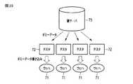
機密情報の書き込みは、例えば、図16のシステムを用いて行われる。図16は、第1実施形態に係る機密情報書き込みシステムを示している。図16に示されるように各ウェハ71用のテスタ72は、鍵(機密情報)サーバ73から、鍵のデータを受け取る。鍵データは、チップごとに相違する。テスタ72は、例えばインターネット等を介して鍵サーバ73と通信可能に接続されている。テスタ72は、受け取った鍵データを、対応するウェハ71中の各機密情報領域34に書き込む。 The confidential information is written using, for example, the system shown in FIG. FIG. 16 shows a confidential information writing system according to the first embodiment. As shown in FIG. 16, the
機密情報とフラグが同一ページ内に割り当てられている場合には、典型的には半導体記憶装置1がページ単位でデータを書き込むように構成されているので、機密情報の書き込みと同時にフラグも機密情報領域34中のフラグ部42に書き込まれる。しかしながら、同時の書き込みは実施形態の本質とは関係ないので、少なくとも上記のように機密情報の書き込み後で半導体記憶装置1の出荷前であれば、フラグは任意のタイミングで書き込まれることが可能である。 When the confidential information and the flag are allocated in the same page, the
機密情報領域34が図15のように構成されている場合、ステップS3は、以下のように行われる。まず、フラグが書かれているかが判定される。すでにフラグが書かれている場合、ステップS3はこれで終了する。一方、フラグが書かれていなければ、機密情報が機密情報領域34に書き込まれる。次いで、フラグが書き込まれ、フラグが正しく書かれたかが判定される。フラグが正しく書かれていない場合、機密情報領域34(典型的には、機密情報領域34のためのブロック)が消去され、機密情報およびフラグの書き込みおよび判定が行われる。ステップS3については、後に詳述する。 When the
次いで、半導体記憶装置1が出荷される(ステップS4)。 Next, the
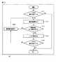
次に、図7および図8を参照して、第1実施形態に係る半導体記憶装置1でのデータ消去シーケンスについて説明する。図7は、第1実施形態に係るシーケンス制御回路23の詳細を例示するブロック図である。図7に示されるように、シーケンス制御回路23は、アクセス制御部51、アドレス比較部52、フラグ判定部53を含んでいる。図8は、第1実施形態に係る半導体記憶装置での消去シーケンスを示すフローチャートである。図8に示されるように、シーケンス制御回路23は、消去コマンドを受信する(ステップS11)。アドレス比較部52は、この消去コマンドに関連するデータ消去対象アドレスを機密情報領域34のアドレスと比較して、機密情報領域34が選択されているかを判定する(ステップS12)。上記のように機密情報領域34中の機密情報は、半導体記憶装置1の出荷後の通常使用の範囲内では、半導体記憶装置1の内部での認証動作に用いられることのみが想定されており、消去されることが想定されていない。そのような消去は禁止されている。また、機密情報の読み出しは、例えば認証の一環として認証回路25からの依頼によって開始され、機密情報領域34が半導体記憶装置1の外部から直接指定されることも想定されておらず、よって機密情報領域34のアドレスは外部に公開されないことが意図されている。したがって、出荷後の通常使用の範囲では機密情報領域34がデータ消去の対象となることはなく、アドレス比較部52による比較結果は、アドレス同士の不一致を示す。アドレス同士が不一致であると、フローはステップS13に移行する。ステップS13において、アクセス制御部51は、関連する要素を制御して指定されたアドレスのデータを消去する(ステップS13)。アクセス制御部51は、指定されたアドレスにデータを書き込み、または指定されたアドレスのデータを消去あるいは読み出すように、半導体記憶装置1の関連する要素を制御する機能を担う。次いで、ステップS13に続いて、データ消去は終了する。 Next, a data erasing sequence in the
一方、不正な手続きを通じて機密情報領域34のアドレスが万一外部に漏洩した場合、機密情報領域34のアドレスを知得した攻撃者が、通常とは異なる何らかの不正な方法で機密情報の消去および更新を試みて、機密情報領域34中のデータの消去を指示することが考えられる。そのような指示がシーケンス制御回路23で受け取られた場合、アドレス比較部52によるステップS12での判定はYESとなる。この結果を受け取ると、アクセス制御部51は、フラグを、例えばシーケンス制御回路23中の図示せぬラッチに転送する(ステップS14)。 On the other hand, if the address of the
次いで、フラグ判定部53は、フラグが立っているかを判定する(ステップS15)。この判定の例については後述する。フラグが立っていない場合、フラグ判定部53はその旨の信号を出力し、処理はステップS13に移行する。フラグが立っていない状況は、典型的には、機密情報の書き込み前のテスト工程(図6のステップS2)中に発生する。ステップS13において、アクセス制御部51は、データを消去する。こうして、機密情報領域34へのデータ消去テストは可能になっている。 Next, the
一方、消去シーケンスが半導体記憶装置1の出荷後である場合、フラグが立っているはずである。アドレス比較部52はこのフラグ信号を出力する。この信号を受け取ると、アクセス制御部51は、指定されたアドレスのデータの消去シーケンスを抜けて(ステップS17)、すなわち指定のアドレスのデータの消去を行わず、次いで消去シーケンスは終了する。すなわち、消去コマンドにより求められる処理を中止する。こうして、機密情報の書き込み後は、機密情報の消去が不能とされている。 On the other hand, if the erase sequence is after shipment of the
出荷後、上記のような消去シーケンスにおいて機密情報領域34以外の領域に対するデータ消去が行われた場合、ステップS11でのコマンド受信からステップS13でのデータ消去を経て消去シーケンスを終了するまでの期間、レディー/ビジーの出力端子(レディー/ビジー端子)からビジー信号が出力される。上記のように、ローレベルおよびハイレベルのレディー/ビジー信号は、例えばそれぞれ半導体記憶装置1のビジー状態およびレディー状態を示す。また、上記のように、機密情報領域34がアクセスされた場合にはデータ消去のステップS13を踏まずに消去シーケンスを抜ける。ここで、ステップS13のデータ消去に要する時間は消去シーケンス全体に要する時間の中で支配的である。したがって図9に示されるように、通常領域32に対するデータ消去を行った場合と比べて機密情報領域34に対するデータ消去を試みた場合では、後者の方が、ステップS13が行われない分、大幅にビジー時間が短い。この特徴を利用して、攻撃者が、機密情報領域34のアドレスを知ることを目的としてアドレスを変えながらデータ消去を試行してレディー/ビジー端子を観測し、機密情報領域のアドレスを特定する等のおそれがある。そこで、図10に示されるように、消去シーケンスを抜ける前にダミーステート(ステップS21)が用意されてもよい。半導体記憶装置1は、ダミーステートにある間、特別な動作を行わず、一定の時間待機し、その後、ステップS17に移行する。こうすることにより、レディー/ビジー端子を介して外部にビジーが出力される継続時間は、従来の継続時間に、ダミービジー継続時間を加えた時間となる。ダミーステートに留まる時間を調整することで、図11に示されるように、機密情報領域34へのデータ消去に対するビジー時間を、半導体記憶装置1の外部に対して、通常領域32へのデータ消去に対するビジー時間と同等に見せることができる。以上のような動作によって、ビジー時間の長短によって攻撃者に機密情報領域34を悟られることを防ぐことが可能となる。 After the shipment, when data erasure is performed for an area other than the
さらに、例えば機密情報領域34が1つのブロックであるとして、ステップS2のテストの結果、このような機密情報ブロックが物理的に不良であった場合の対策について説明する。図12に示されるように、例えば第1機密情報ブロック(領域)34a、第2機密情報ブロック(領域)34b、…というように複数の機密情報ブロックを用意する。これらの複数の機密情報ブロックには、同じ機密情報が記録されている。ステップS2のテスト工程において、第1機密情報ブロック34aが不良であった場合は、第2機密情報ブロック34bが代わりに使用される。また、半導体記憶装置1の出荷後の認証動作の間に第1機密情報ブロック34aが後天性の不良を有する場合も、同様に第1機密情報ブロック34aに代えて第2機密情報ブロック34bが使用される。 Further, for example, assuming that the
また、半導体記憶装置1が、複数のメモリセルアレイ2を有する場合、第1機密情報領域(ブロック)34aと冗長用の第2機密情報領域(ブロック)34bが相違するメモリセルアレイ2に設けられてもよい。図17は、そのような例を示している。図17に示されるように、第1機密情報ブロック34a、第2機密情報ブロック34bは、それぞれ、第1メモリセルアレイ2a、第2メモリセルアレイ2b中に設けられる。 Further, when the
ここまでの説明は、消去の際にフラグが判定される例に関する。上記のように、半導体記憶装置1の出荷時に書き込み済みの機密情報を不正に書き換えるには、基本的には、機密情報の消去が必要であり、セキュリティフラグを用いて機密情報領域34の不正な消去を防止することで間接的に機密情報の不正な書き換えを防止できるからである。しかしながら、この例に代えて、または加えて、機密情報領域34への書き込み指示に対してフラグが判定されてもよい。図18は、第1実施形態に係る半導体記憶装置でのデータ書き込みシーケンスを示すフローチャートである。書き込みシーケンスは、消去シーケンス(図8)と基本的に同じである。異なる点を主に以下に説明する。まず、ステップS11に代えて、ステップS21が行われる。ステップS21において、ステップS11と同様に、シーケンス制御回路23は書き込みコマンドを受信する。次いで、ステップS12に代えて、ステップS22が行われる。ステップS22において、ステップS21と同様に、アドレス比較部52は、書き込みコマンドに関連するデータ書き込み対象アドレスを機密情報領域34のアドレスと比較して、機密情報領域34が選択されているかを判定する。 The description so far relates to an example in which a flag is determined at the time of erasing. As described above, in order to illegally rewrite the confidential information that has been written at the time of shipment of the
ステップS22での判定がNOであると、ステップS13に代えて、ステップS23が行われる。ステップS23において、ステップS13と同様に、アクセス制御部51は、関連する要素を制御して指定されたアドレスにデータを書き込む。一方、ステップS22での判定がYESであると、フローはステップS14に移行する。続くステップS15の判定がNOであると、フローはステップS23に移行する。一方、ステップS15の判定がYESであると、ステップS17に代えて、ステップS27が行われる。ステップS27において、ステップS17と同様に、アクセス制御部51は、書き込みシーケンスを抜ける。 If the determination in step S22 is NO, step S23 is performed instead of step S13. In step S23, as in step S13, the
ここで、図6のステップS3について、図19、図20を用いて、詳述する。図19は、図6のステップS3の詳細なフローである。図20は、第1実施形態に係るフラグの判定前後の状態を例示する。図19に示されるように、フラグ部42に対し、有効なフラグデータが書かれているか否かの判定が行われる(ステップS3−1)。(セキュリティ)フラグは、図20に示されるように、デフォルトで“H”(有効)であって、フラグ判定を行うと“L”(無効)となる。したがって、フラグ部42に有効なフラグデータが書かれていなくてもフラグ判定を行わなければ、フラグは有効のままであり、この結果、機密情報領域34への書き込みおよび消去は不可である。たとえば、フラグが有効な状態で機密情報領域34に消去を試みた場合、図8のシーケンスに従って、アクセス制御部51は消去を行わずに消去シーケンスを抜ける。書き込みを試みた場合には、図18のシーケンスに従い、アクセス制御部51は書き込みを行わずに書き込みシーケンスを抜ける。こうして、ステップS3−1の判定がYESであればステップS3は終了する。 Here, step S3 in FIG. 6 will be described in detail with reference to FIGS. FIG. 19 is a detailed flow of step S3 of FIG. FIG. 20 illustrates a state before and after the flag determination according to the first embodiment. As shown in FIG. 19, it is determined whether or not valid flag data is written in the flag section 42 (step S3-1). As shown in FIG. 20, the (security) flag is “H” (valid) by default, and becomes “L” (invalid) when flag determination is performed. Therefore, even if valid flag data is not written in the
製造後、ステップS3の前までの工程では有効なフラグは書かれていないことが想定されているのでステップS3−1においてフラグ判定を行うと、フラグは“H”から“L”(無効)になる。一方、フラグ部42のメモリセルの閾値電圧が偶然に高い状態となって、結果、ステップS3の前にフラグが書き込み状態になっていた場合にはフラグ判定を行ってもフラグは“H”のままである。このため、このフラグ部42と同じ機密情報領域34に属する情報保持領域41にデータを書きこむことができず、この機密情報領域34については不良と判定される。 Since it is assumed that a valid flag is not written in the process up to step S3 after manufacture, the flag is changed from “H” to “L” (invalid) when flag determination is performed in step S3-1. Become. On the other hand, if the threshold voltage of the memory cell in the
ステップS3−1での判定の結果、フラグが“L”(無効)となると、フローはステップS3−2に移行する。ステップS3−2において、機密情報領域41に機密情報が書き込まれる。フラグが“L”のため、図18のステップS15の判断に基づいて、書き込みステップ(ステップS23)への遷移が可能であり、機密情報の書き込みは可能となっている。 If the result of determination in step S3-1 is that the flag is “L” (invalid), the flow proceeds to step S3-2. In step S3-2, confidential information is written in the confidential information area 41. Since the flag is “L”, it is possible to shift to the writing step (step S23) based on the determination in step S15 in FIG. 18, and the confidential information can be written.
ステップS3−3において、書き込み動作の成否を示すステータス等によって、機密情報が正しく書けたか否かが判定される。機密情報領域41への書き込みが失敗するなどした場合、ステップS3−4において、機密情報領域34が消去される。フラグが“L”(無効)であれば図8のステップS15の判断に基づいて、消去ステップ(ステップS13)への遷移が可能であり、機密情報領域の消去は可能となっている。 In step S3-3, it is determined whether or not the confidential information has been correctly written based on the status indicating the success or failure of the writing operation. If writing to the confidential information area 41 fails, the
ステップS3−3での判断がYES(機密情報の書き込みが完了)であれば、フローは、ステップS3−5に移行する。ステップS3−5において、フラグ部42に有効なフラグデータが書き込まれる。ステップS3−6でフラグデータが書かれているかが判定される。フラグが書かれていない(無効)場合には、ステップS3−4において機密情報領域の消去が行われ、ステップS3−2において機密情報が書き込まれる。いったんフラグが書き込まれた後は機密情報領域34に対して書き込みおよび消去は不可能である。前述のように図8、図18のフラグ判定ステップS15でフラグが書き込み済みであるものと判定されて、アクセス制御部51は消去または書き込みシーケンスを抜けるからである。 If the determination in step S3-3 is YES (writing of confidential information is completed), the flow moves to step S3-5. In step S3-5, valid flag data is written in the
次にフラグの例および読み出されたフラグに対する判定の例について説明する。フラグは、上記のように、特定のビット列とすることができる。または、フラグは、特定のビット列と、この特定のビット列の相補ビット列との組み合わせ(連なり)とすることができる。こうすることによって、フラグの信頼性を高めることができる。すなわち、何らかの原因により、フラグ部42中のあるビットが書き込み状態になっていたとすると、フラグが正しく機能しない。例えば、フラグの書き込み前でも意図せずにフラグが立った状態が生じて、消去テスト時に消去シーケンスが中断されるかもしれない。具体的には、図6の製造ステップ(ステップS1)において製造された直後の半導体記憶装置1において、フラグ部42のセルトランジスタの閾値電圧が高い、すなわちセルトランジスタが書き込み状態になっていることがあり得る。これに対して、特定ビット列と相補ビット列の対応するビット同士の排他的演算結果の例えば“0”(または“1”)の個数が閾値以上であれば、フラグが立っていると判定される。なお、フラグ書き込み前でも、フラグが特定ビット列と相補ビット列を含んだ状態になることも可能性としてはあり得るが、確率は非常に低い。特定ビット列のビット数(同時に相補ビット列のビット数も)を多くすれば、フラグの信頼性は一層高まる。 Next, an example of a flag and an example of determination for a read flag will be described. The flag can be a specific bit string as described above. Alternatively, the flag can be a combination (continuous) of a specific bit string and a complementary bit string of the specific bit string. By doing so, the reliability of the flag can be improved. That is, if a certain bit in the
フラグ部42が複数ビットを含んでいる場合について、より詳細に説明する。制御回路21は、フラグ部42中の各ビットの値と、対応する期待値とを比較し、不一致の数が特定の閾値未満または以下であれば、フラグが有効と判断する。または、制御回路21は、一致の数が特定の閾値超または以上であれば、フラグが有効と判断する。メモリセルが保持する値とその状態のとの対応として、消去状態のメモリセルは“1”を保持し、書き込み状態のメモリセルは“0”を保持するものとする。その上で、フラグの書き込み前はメモリセルは消去状態であってフラグ部42は“1”を保持しているとする。今フラグとして6ビット(F[5]〜F[0])を用意し、フラグは例として“010010“であると仮定する。消去状態では、全てのビットが“1”である。図13に示されるように、フラグを書き込む際に、各ビットに隣接するビットに相補のビット(/F[5]〜/F[0])を書き込む。フラグを読み出す際は、ビットとこれに対応する相補ビットの組の各々について排他的論理和(XOR)が算出される。2入力のXORの論理は、2ビットの極性が異なれば“1”を出力する。1対のビットが互いに相補の値を保持していれば、XORの出力は“1”である。図14に示されるように、F[5]〜F[0]の各々について、対応する相補ビットとの排他的論理和をXORゲート61a〜61fによって取り、6ビットの出力をフラグ判断回路62に入力し、その結果をフラグとする。フラグ判断回路62の判断の基準としては、たとえば、フラグ判断回路62に入力する6ビットの排他的論理和のうち5ビット以上が“1”であった場合には、フラグが書き込み状態にあると判断するようにすればよい。図14の構成は、例えばフラグ判定部53中に設けられる。 A case where the
フラグ部42が複数ビットを含んでいる場合の別の例について説明する。特に、図15のように1ページの全体がフラグ用データに割り当てられている例について説明する。図21は、第1実施形態に係る半導体記憶装置の一部、特にフラグの判定に関する要素を示している。図21に示されるように、半導体記憶装置は、演算器64をさらに含んでいる。ロジック制御回路21は、図1中の要素に加えて、カウンタ/比較器62を含んでいる。図22は、図21の一部の詳細を例示する。図22に示されるように、センスアンプ3は、n+1個のセンスアンプ回路SA0〜SAnを含んでいる。演算器64は、n+1個の演算回路OP0〜OPnを含んでいる。ページバッファ4は、n+1個のデータラッチAD0〜ADn、n+1個のデータラッチBD0〜BDn、n+1個のフラグラッチFLG0〜FLGnを含んでいる。センスアンプ回路SA0、演算回路OP0、データラッチAD0、BD0、フラグラッチFLG0は、ビット線BL0用に設けられている。同様に、センスアンプ回路SAi、演算回路OPi、データラッチADi、BDi、フラグラッチFLGiは、ビット線BLiのために設けられている。iは、0または1〜nの自然数である。フラグラッチFLG0〜FLGnは、それぞれスイッチSW0〜SWnを介してバスFLGBUSに接続されている。バスFLGBUSは、カウンタ/比較器62に接続されている。動作は、以下の通りである。以下の動作は、例えば、シーケンス制御回路23により制御される。 Another example when the
フラグ部42中の有効なビットは、特定のデータ(例えば“1”または“0”)を保持しているものとする。まず、フラグ部42中の複数ビットのデータが、それぞれデータラッチAD0〜ADnに読み出される。有効なフラグと同じ値が、ロジック制御回路21からデータラッチBD0〜BDnにセットされる。演算回路OP0は、データラッチAD0、BD0中のデータの排他的論理和XORを算出し、結果をフラグラッチFLG0に保持する。データラッチAD0中のデータとデータラッチBD0中のデータが異なれば、XORの結果は“1”である。同様に、演算回路OPiは、データラッチADi、BDi中のデータの排他的論理和XORを算出し、結果をフラグラッチFLGiに保持する。スイッチSW0がオンされて、フラグラッチFLG0中のデータがカウンタ/比較器62に供給される。カウンタ/比較器62は、受け取ったデータが“1”であれば、1をインクリメントする。同様に、スイッチSW1〜SWnが順次オンされて、結果、フラグラッチFLG0〜FLGn中の“1”データの個数が計数される。すなわち、1ページ中のフェイルビットの個数が得られる。カウンタ/比較器62は、パラメータレジスタ24から、1ページ中のフェイルビットの許容数と等しい基準値を受け取る。カウンタ/比較器62は、基準値と、1ページ中のフェイルビットの個数を比較する。カウンタ/比較器62は、個数が基準値以下であれば判定パスの旨の信号をロジック制御回路21に送信し、個数が基準値を超えていれば判定フェイルの旨の信号をロジック制御回路21に送信する。 It is assumed that valid bits in the
ここで、フラグを読み出して判定する機能をもつ回路について、半導体記憶装置に備わっているパワーオンリードを制御する回路の一部の機能を用いることが可能である場合には、これを用いてもよい。用いることが可能な場合には、回路面積の増加を抑える効果がある。 Here, for a circuit having a function of reading and determining a flag, a part of the function of the circuit for controlling the power-on read provided in the semiconductor memory device can be used. . When it can be used, there is an effect of suppressing an increase in circuit area.
また、フラグを読み出して判定する機能を持つ回路について、半導体記憶装置に備わっているベリファイ読み出し機能で未書き込みビットを計数する回路を用いることが可能である場合には、これを用いてもよい。 In addition, a circuit having a function of reading and determining a flag may be used when a circuit that counts unwritten bits by a verify read function provided in a semiconductor memory device can be used.
以上説明したように、実施形態に係る半導体記憶装置1では、メモリセルアレイ2はデータ消去状態からのみデータを書き込み可能であり、機密情報領域34は機密情報の書き込み後は有効なフラグを含んでいる。半導体記憶装置1は、機密情報領域34を指定するデータ消去を指示されるとフラグを判定し、フラグが立っている場合はデータ消去を行わない。半導体記憶装置1は、このような処理を行うシーケンス制御回路23を含んでいる。したがって、機密情報領域34中の機密情報が消去されることが禁止され、ひいては機密情報の書き換えが防止される。さらに、機密情報領域34を指定するデータ書き込みの指示に対しても、フラグが立っている場合、半導体記憶装置1はデータ書き込みを行わない。これにより、機密情報領域34の保護がより向上する。また、フラグは、テスト工程後に書き込まれる。このため、テスト時の機密情報領域34中のデータの消去は可能であり、テストの実施と機密情報の消去禁止を両立できる。 As described above, in the
ここまで説明してきた認証機能を備えたメモリは、通常当該の機能を備えたホストにコントローラを介して接続される。しかし、認証機能を用いない用途でこの認証機能を備えたメモリを使用する場合もある。この場合に、認証機能を用いないからといって、機密情報領域に何もデータが書かれていない状態(いわゆる白ロム)であると、攻撃者がこの領域に認証をパスするようなデータを書き込んで、あたかも正当なメモリであるかのように成りすましたメモリを製造される恐れがある。また、機密情報領域34に、通常の認証機能を備えたメモリと同様に機密情報を書いておくことも、機密情報が漏洩するリスクが増すから好ましくない。この場合は機密情報領域34にダミーのデータとフラグをあらかじめ書き込んでおき、このメモリに対して通常の(認証機能なし)コントローラを用いる場合には特に問題は生じない。しかし、認証機能付きのコントローラを用いて通常用途(認証機能なし)に対応させる場合には次のようにする。認証回路25は通常と同様に認証のシーケンスを行い、演算の結果を半導体記憶装置1の外部のコントローラに出力する。ダミーのデータを元に演算を行った結果は通常では認証フェイルと判断されるものであるが、認証機能を用いない用途で使用する場合には、コントローラは認証結果を無視して、動作を行うようにすればよい。 The memory having the authentication function described so far is normally connected to a host having the function via a controller. However, a memory having this authentication function may be used for applications that do not use the authentication function. In this case, if the authentication function is not used, if no data is written in the confidential information area (so-called white ROM), the data that the attacker passes authentication to this area There is a risk of writing and producing a memory that looks as if it were legitimate memory. In addition, it is not preferable to write confidential information in the
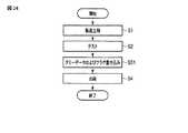
ダミーデータの書き込みは、図23のシステムを用いて行われる。図23は、図16のシステムと同じである。異なるのは、図16の鍵データに代えて、ダミーデータがテスタ72に供給されることである。ダミーデータは、一部または全部のウェハにおいて同じであってもよいし、異なっていてもよい。ダミーデータの書き込みのフローについても、図24に示されるように、機密情報の書き込みと同じタイミングで行われる。図24は、第1実施形態に係る半導体記憶装置の製造から出荷までの工程の別の例のフローチャートである。図24では、図6のステップS3に代えて、ステップ31が行われる。ステップS31において、機密情報領域34にダミーデータおよびフラグが書き込まれる。 The dummy data is written using the system shown in FIG. FIG. 23 is the same as the system of FIG. The difference is that dummy data is supplied to the
このような運用によって、実施形態に係る認証機能を有する半導体記憶装置を、通常(認証機能なし)の半導体記憶装置として使用することができる。すなわち、実施形態に係る半導体記憶装置を、認証機能付用途と通常(認証機能なし)用途に利用できる。認証機能なしの用途では、従来のフロー(図25)に対して、ダミーデータおよびフラグ書き込みステップ(S31)が付加される。この点が、実施形態のフローでは、従来のフローとで異なる。 By such operation, the semiconductor memory device having the authentication function according to the embodiment can be used as a normal (no authentication function) semiconductor memory device. That is, the semiconductor memory device according to the embodiment can be used for an application with an authentication function and a normal application (no authentication function). In applications without an authentication function, dummy data and flag writing step (S31) is added to the conventional flow (FIG. 25). This point is different from the conventional flow in the flow of the embodiment.
(第2実施形態)
第2実施形態は、各種フラグの格納方法に関する。(Second Embodiment)
The second embodiment relates to a method for storing various flags.
第1実施形態に係るフラグは、このフラグが含まれる機密情報領域34中の情報保持部41中への消去および/または書き込みの許否を示すためのものであり、以下、これを消去/書き込みフラグと称して、「フラグ」との呼称と区別する。半導体記憶装置1には、消去/書き込みフラグ以外にも種々のフラグが定義されている場合がある。フラグは、一般に、各ページ中に書き込まれていることが多く、書き込まれているページに関する種々の情報を示す。 The flag according to the first embodiment is used to indicate whether or not erasure and / or writing into the information holding unit 41 in the
フラグの例には、LMフラグ、スマートベリファイ(SV)フラグ等が含まれる。LMフラグは、LMフラグが含まれている物理ページがアッパーページまで書き込まれているかを示すためのものである。LMフラグは、例えば、1ビットの情報で表現される。この1ビット情報は、例えば図26に示されるように、8ビット(1カラム)にて表示される。図26は、通常領域(例えば通常領域32)の一例を示す。図では、通常領域は、1つのブロックBKからなる。図26に示されるように、通常領域中の各物理ページは、情報保持部(ユーザデータ保持部)101と、フラグ部102を含んでいる。情報保持部101は、ユーザデータを保持する。フラグ部102は、LMフラグ領域102A、SVフラグ領域102Bを含んでいる。LMフラグ領域102Aは、両端を除く6ビットの全てにおいて、“0”フラグを表示するために“0”を保持し、“1”フラグを表示するために“1”を保持する。LMフラグの判別は、1組8ビットに含まれる“0”ビットまたは“1”ビットのいずれが多いかを通じて行われる。このため、この文脈では、最大3ビットの誤りまで許容可能である。一方で、カラム単位での不良に弱く、また誤り対策のために情報量(表示用のビット数)を多くすると多数決を判定するための回路の面積も大きくなる。 Examples of the flag include an LM flag and a smart verify (SV) flag. The LM flag indicates whether a physical page including the LM flag has been written up to the upper page. The LM flag is expressed by 1-bit information, for example. This 1-bit information is displayed in 8 bits (1 column) as shown in FIG. 26, for example. FIG. 26 shows an example of a normal area (for example, the normal area 32). In the figure, the normal area consists of one block BK. As shown in FIG. 26, each physical page in the normal area includes an information holding unit (user data holding unit) 101 and a
SVフラグは、例えば4ビットの情報で表現され、例えば8ビットにて表示され、例えばロワーページへの書き込みに関する情報、例として書き込みの際の書き込みのループ回数(ひいては、書き込みの成功に繋がった書き込み電圧の大きさ)を保持する。ロワーページへの書き込みの情報を使用してアッパーページへの書き込みのための電圧を調整することを通じて、アッパーページへの書き込みの効率を向上できる。SVフラグ領域102Bの前半の4ビットは、SVフラグそのものを示し、後半の4ビットは前半の4ビットのそれぞれの相補ビットである。SVフラグの判別は、前半4ビットが、後半4ビットと正しく相補になっているかの判定を通じて行われる。このため、この文脈では、8ビット中で1ビットの誤りも許容されない。2ビットの誤りが存在すると、誤判定(間違った値で判定パス)が生じ、この誤判定を検知することはできない。 The SV flag is expressed by, for example, 4-bit information, and is displayed by, for example, 8 bits. For example, information related to writing to the lower page, for example, the number of write loops at the time of writing (and thus writing that has led to successful writing) Voltage magnitude). The efficiency of writing to the upper page can be improved by adjusting the voltage for writing to the upper page using the information of writing to the lower page. The first 4 bits of the
このようにフラグの誤書き込みの防止が求められる。そのために、フラグ書き込み後にフラグ部102に対してのみ特別なチェックが行われる。すなわち、誤書き込みの無いことを保証するようにフラグが書き込まれる。しかしながら、このような書き込みは、書き込み性能の劣化を招く。誤り対策用に、フラグ当たりの情報量を増やす(2以上のカラムで表示する)ことも考えられる。しかしながら、カラム数を増やすためには、物理ページを増やす必要があり、その実施は容易ではない。フラグ部102を増やすために情報保持部101を縮小することもできない。ユーザの利便性を損なうからである。以上の背景に基づいてなされた第2実施形態について、以下に説明する。 Thus, prevention of erroneous writing of flags is required. Therefore, a special check is performed only on the
図27は、第2実施形態に係る通常領域の一部を示している。図27に示されるように、1ブロック(例えば128の物理ページを含む)に対して、このブロックと関連付けられた1つの物理ページ(管理情報ページと称する)111が設けられる。管理情報ページ111も通常領域32の一部である。管理情報ページ111は、この管理情報ページ111と関連付けられたブロックBK中の全てのページPGの全ての管理情報(フラグ)を保持する。フラグとして、LMフラグおよびSVフラグが例として用意されている。しかしながら、他の任意のフラグを使用することが可能である。ブロックBK中の物理ページPGは、対応するフラグを含んでおらず、情報保持ページ112と称する。例として、LMフラグは1ビットにより表現され、SMフラグは4ビットにより表現される。フラグの種類および表現の仕方は、以下の例に制限されず、任意のものが本実施形態に適用可能である。 FIG. 27 shows a part of the normal area according to the second embodiment. As shown in FIG. 27, for one block (for example, including 128 physical pages), one physical page (referred to as a management information page) 111 associated with this block is provided. The management information page 111 is also a part of the
管理情報ページ111は、対応するブロックBK中の物理ページPG0〜ページPG127の各々の管理情報用の区画を含んでいる。物理ページPG0〜PG127用領域は、典型的には、昇順に並んでいる。物理ページPG0〜PG127用領域の各々は、例えば、物理ページPG0用領域について図27に代表的に示す構造と同じ構造を有する。しかしながら、相違する領域が相違する構造を有していてもよい。 The management information page 111 includes a management information section for each of the physical pages PG0 to PG127 in the corresponding block BK. The areas for physical pages PG0 to PG127 are typically arranged in ascending order. Each of the areas for physical pages PG0 to PG127 has the same structure as that typically shown in FIG. 27 for the area for physical page PG0. However, different regions may have different structures.
物理ページPG0用領域は、さらに、物理ページPG0についての全ての管理情報の各ビット用の区画へと分割されている。第1区画(Flag[0])は、LMフラグの1ビット(LM)に割り当てられている。第2〜第5区画(Flag[1]〜Flag[4])は、それぞれ、SVフラグの第1〜第4ビット(SV[0]〜SV[3])に割り当てられている。残りの区画はその他の任意の管理情報のビットに割り当てられ、管理情報に割り当てられない区画はスペアとして予約されている。1ページの長さが65536ビット(=8192バイト)とすると、管理情報ページ111が128の物理ページのための管理情報を保持することに基づいて、物理ページPG0〜PG127用領域の各々は、m=64の管理情報ビットを保持できる。 The physical page PG0 area is further divided into sections for each bit of all management information for the physical page PG0. The first section (Flag [0]) is assigned to 1 bit (LM) of the LM flag. The second to fifth sections (Flag [1] to Flag [4]) are assigned to the first to fourth bits (SV [0] to SV [3]) of the SV flag, respectively. The remaining partitions are assigned to bits of other arbitrary management information, and the partitions not assigned to the management information are reserved as spares. Assuming that the length of one page is 65536 bits (= 8192 bytes), each of the areas for physical pages PG0 to PG127 is based on the fact that the management information page 111 holds management information for 128 physical pages. = 64 management information bits can be held.
図27は、第1〜第5区画(Flag[0]〜Flag[4])がそれぞれ、“0”、“0”、“1”、“1”、“0”を保持している例を示す。すなわち、LMフラグ=0、SVフラグ=4´b0110が保持されている。各区画は、例えばn=8ビット(1カラム)からなる。すなわち、管理情報の1ビットは、1カラムにより表示される。管理情報ビット“1”は、全て“1”のビットにより表示される。ただし、後述のように、管理情報ビットの判定は、“1”ビットの数がある閾値を超えていることを以て判定する。このため、必ずしも全ビットが“1”ではなく、図でもそのように描かれている。一方、管理情報ビット“0”は、8ビットのランダムデータにより表示される。ランダムデータは、1ビットの情報を、任意のアルゴリズムにより生成された特定の複数ビット(本文脈ではnビット)で表現されたデータを指す。 FIG. 27 shows an example in which the first to fifth sections (Flag [0] to Flag [4]) hold “0”, “0”, “1”, “1”, and “0”, respectively. Show. That is, the LM flag = 0 and the SV flag = 4′b0110 are held. Each partition is composed of, for example, n = 8 bits (one column). That is, one bit of management information is displayed by one column. All the management information bits “1” are indicated by “1” bits. However, as will be described later, the management information bit is determined based on the fact that the number of “1” bits exceeds a certain threshold. For this reason, all the bits are not necessarily “1”, and are drawn as such in the figure. On the other hand, the management information bit “0” is displayed by 8-bit random data. Random data refers to data in which 1-bit information is expressed by a specific plurality of bits (n bits in this context) generated by an arbitrary algorithm.
図28は、第2実施形態に係る管理情報ページ判定のシーケンスの例を示している。図28の最上段は、管理情報ページ読み出しを伴わない、従来のデータ読み出しのシーケンスを示している。まず、コマンド00h(読み出しコマンド)、読み出し対象の1以上の論理ページのそれぞれのアドレスAdd、コマンド30h(アドレス終了コマンド)が、半導体記憶装置1の外部のコントローラから半導体記憶装置1に供給される。これに応答して、シーケンス制御回路23は、関連する要素を制御して、アドレスにより指定された論理ページのデータを半導体記憶装置1の外部に出力する。第2段、第3段、最下段は、管理情報ページ判定を伴うシーケンスの例を示す。第2段は、従来の読み出しに管理情報ページ判定が一律に付加される例を示す。第2段に示されるように、半導体記憶装置1は、コマンド00h、アドレス、コマンド30hを受け取ると、データ読み出しに先立って管理情報ページ読み出しを行う。シーケンス制御回路23は、管理情報ページ中の管理情報を、例えばシーケンス制御回路23中のレジスタ(例えばパラメータレジスタ24)に保持する。管理情報ページ読み出しについては後述する。続いて、シーケンス制御回路23は、レジスタに保持された管理情報(例えばLMフラグ)に基づいて定まる読み出しを行う。図では、データの読み出しについて示しているが、データの書き込みについても同じである。すなわち、書き込みに際して、シーケンス制御回路23は、管理情報ページを読み出し、これをレジスタに保持し、レジスタ中の管理情報(例えばSVフラグ)に基づいて定まる書き込みを行う。以下の第3段、最下段についても同じである。 FIG. 28 shows an example of a management information page determination sequence according to the second embodiment. The uppermost part of FIG. 28 shows a conventional data read sequence that does not involve management information page read. First, a
第3段は、管理情報ページ読み出し用のコマンドが設けられた例を示している。外部コントローラは、管理情報ページ読み出しに際して、専用コマンド(21h)を、半導体記憶装置1に供給する。シーケンス制御回路23は、コマンド21hを認識可能に構成されている。外部コントローラは、コマンド21hに続いて、コマンド00h、アドレス、コマンド30hを半導体記憶装置1に供給する。シーケンス制御回路23は、コマンド21hが最初に受け取られたことに基づいて、読み出し対象の論理ページについての管理情報を含んだ管理情報ページ111を読み出し、例えばシーケンス制御回路23中のレジスタ(図示せず)に保持する。コマンド00hに先立つコマンド21hが不在の場合、従来と同じく、指定されたページからデータが読み出される。その後、読み出し指示に対して、シーケンス制御回路23は、第1段についての説明と同様に、レジスタ中の管理情報に基づいて定まる読み出しを行う。 The third row shows an example in which a management information page read command is provided. The external controller supplies a dedicated command (21h) to the
最下段も、管理情報ページ判定用のコマンドが設けられた例を示している。この例では、コマンド00hに先立ってコマンド21hが存在する場合、シーケンス制御回路23は、読み出し対象の論理ページに関連する管理情報ページを読み出し、管理情報をレジスタに保持し、レジスタ中の管理情報に基づいて定まる読み出しを行う。コマンド00hに先立つコマンド21hが不在の場合、従来と同じく、指定された論理ページからデータが読み出される。 The bottom row also shows an example in which a management information page determination command is provided. In this example, when the
図29は、第2実施形態に係る管理情報ページ読み出しのフローチャートである。図29のフローは、例えば、シーケンス制御回路23により行われる。すなわち、図28の第2段から最下段のいずれが実装されているかに基づいて、シーケンス制御回路23が、管理情報ページ読み出しの指示を認識すると、図29の管理情報ページ読み出しを行う。シーケンス制御回路23は、管理情報ページ読み出しの指示を認識すると、パラメータiを0にリセットするとともに、後に読み出される管理情報ページ中の管理情報を保持するレジスタ中の値(Flag[0]〜Flag[m-1])を消去状態に初期化する(ステップS41)。パラメータiは、区画の番号を示し、例えばシーケンス制御回路23中のカウンタ/レジスタにより保持される。シーケンス制御回路23は、管理情報ページ中のデータを読み出し、これを例えば半導体記憶装置1中のRAM(Random Access Memory)に保持する(ステップS42)。 FIG. 29 is a flowchart of management information page reading according to the second embodiment. The flow in FIG. 29 is performed by the
次に、シーケンス制御回路23は、i番目の区画中の“0”ビットの個数が、ある閾値以下であるかを判断する(ステップS43)。“0”ビットの個数が閾値以下であれば、判断対象の区画はランダムデータを保持しないと判断され、フローは、ステップS47に移行する。非ランダムデータが保持されていれば、本来は区画中の全ビットは消去状態(“1”状態)のはずだが、実際はいくつかのビットが反転し得る。このため、全ビットが“1”であるかの判定に代え、“0”ビットの個数が許容数以下であれば、区画は消去状態であると判定される。ステップS47において、シーケンス制御回路23は、i番目の区画に対応する管理情報ビットのためのレジスタにおいて“1”(無効)を設定する。ステップS47は、ステップS48に続く。 Next, the
ステップS43での判断がNOであれば、フローはステップS45に移行する。ステップS45において、シーケンス制御回路23は、i番目の区画中の“1”ビットの個数が、ある閾値以下であるかを判断する。“1”ビットの個数が閾値以下であれば、判断対象の区画はランダムデータを保持しないと判断され、フローは、ステップS47に移行する。一方、“1”ビットの個数が閾値を超えていれば、これは“0”ビットの個数も“1”ビットの個数も閾値を超えていることを意味する。これに基づいて、判断対象のi番目の区画はランダムデータ(すなわち“0”ビットを表示)であると判定される。この結果、シーケンス制御回路23は、i番目の区画に対応する管理情報ビットのためレジスタにおいて“0”(有効)をセットする(ステップS46)。ステップS46は、ステップS48に続く。If the determination in step S43 is no, the flow moves to step S45. In step S45, the
ステップS48において、シーケンス制御回路23は、パラメータiがm−1であるか、すなわち全ての区画が判定されたかを判断する。ステップS48での判断がNOであれば、シーケンス制御回路23は、パラメータiを1増分し(ステップS49)、ステップS43に移行する。ステップS48での判断がYESであれば、管理情報ページ読み出しは終了する。 In step S48, the
以上説明したように、第2実施形態に係る半導体記憶装置によれば、2以上の物理ページ(例えば1ブロック中の全物理ページ)についての全ての管理情報(フラグ)が、1つの物理ページにまとめられる。このため、m(1ページあたりの管理情報ビット数)を減じるだけで、n(1管理情報ビットを表示するためのビット数)を増やすことができる。nを増やすことにより、管理情報の読み出しエラー耐性を向上できる。そのためにメモリセルアレイのデザインの変更(ページ長の増加)は不要である。As described above, according to the semiconductor memory device of the second embodiment, allmanagement information ( flags) for two or more physical pages (for example, all physical pages in one block) arestored in one physical page. It is put together. Therefore, n (the number of bits for displaying one management information bit) can be increased only by reducing m (the number of management information bits per page). By increasing n, management information read error tolerance can be improved. Therefore, it is not necessary to change the design of the memory cell array (increase in page length).
また、管理情報ビットの判定は、対応する区画中のランダムデータの有無を通じて行われる。ランダムデータの有無の判定は、“0”および/または“1”ビットのスキャンおよび閾値との比較により行われる。このビットスキャンや閾値との比較は、書き込みおよび消去用に元々備わっているビットスキャン回路を用いて行われる。このため、管理情報ビットの判定に、新たな回路を設ける必要は無い。 The management information bit is determined through the presence or absence of random data in the corresponding partition. The presence / absence of random data is determined by scanning “0” and / or “1” bits and comparing with a threshold value. The bit scan and comparison with the threshold value are performed using a bit scan circuit originally provided for writing and erasing. For this reason, it is not necessary to provide a new circuit for determining the management information bit.
(第3実施形態)
第2実施形態は、ページごとの管理情報すなわちフラグをまとめることに関する。第3実施形態は、ブロックに関する管理情報を1ページにて表示することに関する。(Third embodiment)
The second embodiment relates to grouping management information, that is, flags for each page. The third embodiment relates to displaying management information related to blocks on one page.
図30は、第3実施形態に係る通常領域の一部を示している。図30に示されるように、第2実施形態と同様に、通常領域用の1ブロック(通常ブロック)に対して、このブロックと関連付けられた1つの管理情報ページ111が設けられる。管理情報ページ111は、第2実施形態と同じく、複数の区画を含んでいる。いくつの区画を含んでいるかは、管理情報ページ111が保持する管理情報ビットの数と一致する。図30は、16の管理情報ビットの例に関する。1ページが8192バイト(=65536ビット)の例では、各区画は、512カラム(バイト)の大きさを有する。例として、16の管理情報ビットのうちの1ビットは、書き込み可/不可を表現するフラグとして機能し、残りの15ビットは消去/書き込み回数を表示する。例えば、第1区画(protect)は、消去可/不可を示す1ビットに割り当てられる。第2〜第16区画(W/E[0]〜W/E[14])は、消去/書き込み回数を示す15ビットの各ビットに割り当てられる。各区画は、第2実施形態と同じく、対応する管理情報ビットが“1”であることを表示するために、実質的に全て“1”ビットの情報を保持し、対応する管理情報ビットが“0”であることを表示するためにn=4096ビットのランダムデータを保持する。FIG. 30 shows a part of the normal area according to the third embodiment. As shown in FIG. 30, as in the second embodiment, one management information page 111 associated with this block is provided for one block (normal block) for the normal area. The management information page 111 includes a plurality of sections as in the second embodiment. How many partitions are included matches the number of management information bits held in the management information page 111. FIG. 30 relates to an example of 16 management information bits. In an example where one page is 8192 bytes (= 65536 bits), each partition has a size of 512 columns (bytes). As an example, 1 bit out of 16 management information bits functions as a flag indicating whether writing is possible or not, and the remaining 15 bits indicate the number of times of erasing / writing. For example, the first partition (protect) is assigned to 1 bit indicating whether or not erasure is possible. The second to sixteenth sections (W / E [0] to W/ E [14]) are assigned to 15 bits each indicating the number of erase / write operations. As in the second embodiment, each partition holds substantially all “1” information to indicate that the corresponding management information bit is “1”, and the corresponding management information bit is “1”. to indicate that a 0 "for holding the n = 4096bit random data.
管理情報ページ111は、特定のタイミングで読み出される。例えば、シーケンス制御回路23は、外部のコントローラの指示に従って、半導体記憶装置1の電源投入後に半導体記憶装置1中の全てまたは一部の管理情報ページ111を読み出す。シーケンス制御回路23は、第2実施形態(図29)と同様に、読み出された管理情報ページについて、各区画中の“0”ビットおよび“1”ビットの個数をそれぞれの閾値と比較する(ステップS43、S45に対応)。シーケンス制御回路23は、この比較を通じて、各区画中にランダムデータが保持されているかを判断し、対応する管理情報ビットが“0”であるか“1”であるかを決定する。決定された管理情報は、例えばシーケンス制御回路23中のレジスタに保持される(ステップS46、S47に対応)。または、第2実施形態の図28と同様に、管理情報ページ111の読み出しは、シーケンス制御回路23によって特定のタイミングで開始される。すなわち、図28の第2段と同様に、ある通常ブロックへの書き込みまたは消去が指示されると、シーケンス制御回路23は、その書き込みまたは消去に先立って一律に、対応する管理情報ページを読み出す。対応するブロックが書き込み(および/または消去)不可に設定されていれば、シーケンス制御回路23は、書き込みおよび/または消去を実行しない。The management information page 111 is read at a specific timing. For example, the
消去/書き込み回数についても同様である。すなわち、例えば、通常ブロックへの消去/書き込みが指示されると、シーケンス制御回路23は、各区画中にランダムデータが保持されているかの判断を通じて各ビットの“0”または“1”を判定し、判定された値をレジスタに保持する。 The same applies to the number of erase / write operations. That is, for example, when erasing / writing to a normal block is instructed, the
以上説明したように、第3実施形態に係る半導体記憶装置によれば、ブロックに関する管理情報が管理情報ページにおいて保持される。このため、第2実施形態と同じく、管理情報ビットの定義(種類やnの数)の変更が容易である。また、やはり第2実施形態と同じく、管理情報ビットの判断に新たな回路が必要無い。 As described above, according to the semiconductor memory device according to the third embodiment, the management information regarding the block is held in the management information page. For this reason, as in the second embodiment, it is easy to change the definition (type and number of n) of management information bits. Also, as in the second embodiment, no new circuit is required for determining the management information bit.
(第4実施形態)
上記のように、半導体記憶装置1の製造後で出荷前には機密情報領域34に機密情報が書き込めるとともに、出荷後には機密情報領域34の消去および/または書き込みが禁止される必要がある。このことを背景として、第4実施形態は、機密情報領域用のブロック(機密情報ブロック)への管理情報ページの適用に関し、第1実施形態の一部の詳細に関する。(Fourth embodiment)
As described above, confidential information can be written into the
図31は、第4実施形態に係る機密情報領域の一部を示している。図31に示されるように、機密情報ブロック121は、管理情報ページ122を含んでいる。管理情報ページ122は、例えば、機密情報ブロック121中の最終ページである。機密情報ブロック121中の残りの物理ページは、情報保持ページ123であり、機密情報を保持する。管理情報ページ122は、全体で、第1実施形態のフラグ(消去/書き込みフラグ)を保持する。消去/書き込みフラグは、対応する機密情報ブロック121の消去および/または書き込みの可または不可を示す。 FIG. 31 shows a part of the confidential information area according to the fourth embodiment. As shown in FIG. 31, the confidential information block 121 includes a management information page 122. The management information page 122 is the last page in the confidential information block 121, for example. The remaining physical page in the confidential information block 121 is an information holding page 123, which holds confidential information. The management information page 122 holds the flag (erase / write flag) of the first embodiment as a whole. The erase / write flag indicates whether the corresponding confidential information block 121 can be erased and / or written.
消去/書き込みフラグは、管理情報ページ122全体に亘るランダムデータを用いて表示される。すなわち、管理情報ページ122の全体が、消去状態であれば、実際には後述のように閾値以下の個数の“0”ビットを含んでいれば、消去/書き込みフラグは“1”(消去/書き込み可)である。他方、管理情報ページ122にランダムデータが保持されていれば、消去/書き込みフラグは“0”(消去/書き込み不可)である。The erase / write flag is displayed using random data over the entire management information page 122. That is, the overall management information page 122, if the erase state, if indeed contain"0" bits of the number ofsubthreshold than as described below, the erase / write flag "1" (erased / it iswritable). On the other hand, if the random data is retained in the management information page 122,the erase / write flag is "0" (erase /unwritable).
図32は、第4実施形態に係る管理情報読み出しのフローチャートである。図32のフローは、半導体記憶装置1の出荷前および後に関し、時間に沿って以下に説明する。なお、フローの開始の時点では、例えば機密情報ブロックに機密情報は書き込まれていない。また、例えば半導体記憶装置1に何らデータは書かれておらず、したがって、管理情報ページ122も消去状態である。 FIG. 32 is a flowchart of management information reading according to the fourth embodiment. The flow of FIG. 32 will be described below along the time with respect to before and after shipment of the
図32に示されるように、半導体記憶装置1は、管理情報ページの読み出しコマンドを受け取る(ステップS51)。このコマンドは、出荷前の使用を想定されており、出荷後のユーザによる使用は想定されておらず、公開もされていない。コマンド受信に応答して、シーケンス制御回路23は、後に読み出される管理情報ページ中の管理情報(消去/書き込みフラグ)を保持するレジスタを消去状態に初期化する(ステップS52)。レジスタは、例えばシーケンス制御回路23中に設けられ、例えばパラメータレジスタ24である。次いで、シーケンス制御回路23は、関連する要素を制御して、管理情報ページ122中のデータを読み出し、これを例えば半導体記憶装置1中のRAMに保持する(ステップS53)。シーケンス制御回路23は、ステップS43と同様に、読み出されたデータ中の“0”ビットの個数が、ある閾値以下であるかを判断する(ステップS54)。“0”ビットの個数が閾値以下であれば、管理情報ページ122はランダムデータを保持しない、すなわち消去/書き込みフラグは無効であると判断される。この判断に基づいてフローは、ステップS55に移行する。上記のように、最初にステップS54に到達したとき、管理情報ページ122は消去状態であり、よってフローはS55に移行する。 As shown in FIG. 32, the
ステップS55において、シーケンス制御回路23は、消去/書き込みフラグを保持するレジスタに“1”(無効)を設定する。次に、シーケンス制御回路23は、機密情報を外部から受け取り、これを機密情報ブロックに書き込む(ステップS56)。機密情報ブロックへの書き込み(および/または消去)の指示を受け取ると、シーケンス制御回路23は、レジスタ中の消去/書き込みフラグを参照する。レジスタ中の消去/書き込みフラグが無効であれば、シーケンス制御回路は、書き込み(消去)を行う。シーケンス制御回路23は、レジスタ中の消去/書き込みフラグが不可を示していると、機密情報ブロックへの書き込み(および/または消去)を行えないように構成されている。ステップS56の段階では、消去/書き込みフラグは無効なので、機密情報の書き込みは成功する。続いて、シーケンス制御回路23は、例えば半導体記憶装置1の外部から受信したコマンドに応答して、管理情報ページ122にランダムデータを書き込む(ステップS59)。この段階でも、消去/書き込みフラグは無効なので、管理情報ページ122への書き込みは許可される。こうして、第4実施形態に関する出荷前のフローは終了する。 In step S55, the
続いて出荷後について説明する。出荷後、管理情報ページ122はランダムデータを保持している。ユーザが、管理情報ページ読み出しコマンドを不正に入手および使用すると、ステップS51が開始する。ステップS51、S52(レジスタ初期化)、S53(管理情報ページ読み出し)を経て、フローはステップS54に移行する。ステップS54の判断の結果、“0”ビットの個数は閾値以上のはずである。管理情報ページ122は、ランダムデータを保持しているからである。この結果、フローは、ステップS61に移行する。 Next, after shipping will be described. After the shipment, the management information page 122 holds random data. If the user illegally obtains and uses the management information page read command, step S51 starts. After steps S51, S52 (register initialization) and S53 (management information page read), the flow proceeds to step S54. As a result of the determination in step S54, the number of “0” bits should be greater than or equal to the threshold value. This is because the management information page 122 holds random data. As a result, the flow moves to step S61.
ステップS61において、シーケンス制御回路23は、ステップS45と同様に、読み出されたデータ中の“1”ビットの個数がある閾値以下であるかを判断する。管理情報ページ122がランダムデータを保持していることに基づいて、“1”ビットの個数も閾値を超えているはずである。ステップS54、61の判断を通じて管理情報ページがランダムデータを保持していることに基づいてフローはステップS63に移行する。ステップS63において、シーケンス制御回路23は、消去/書き込みフラグを保持するレジスタに“0”(有効)を設定する。消去/書き込みフラグ保持レジスタが消去/書き込み不可の旨の値を保持している。このため、不正なユーザが、機密情報ブロックに書き込み(および/または消去)を行おうとしても、これは禁止される。すなわち、管理情報ページ122がランダムデータを保持していると、フローは、ステップS55に到達できない。したがって、不正なユーザは、レジスタ中の消去/書き込みフラグを可へ設定することができず、ひいては機密情報ブロックの書き換えも不能である。また、シーケンス制御回路23は、レジスタ中の消去/書き込みフラグの設定を図32のフローを介してのみ行えるように構成されている。このため、やはり不正なユーザは、機密情報ブロックに書き込みを行えない。 In step S61, the
ステップS61において、“1”ビットの個数が、ある閾値以下であれば、フローはステップS55に移行する。 In step S61, if the number of “1” bits is equal to or smaller than a certain threshold value, the flow proceeds to step S55.
以上説明したように、第4実施形態に係る半導体記憶装置によれば、管理情報ページ122が設けられる。管理情報ページ122は、ランダムデータを保持するか消去状態であるかに基づいて定まる消去/書き込みフラグを保持する。半導体記憶装置1の製造後の初期段階では管理情報ページ122が消去状態であるため、これに基づいてレジスタ中の消去/書き込みフラグは可に設定され、機密情報ブロック121への書き込みが可能である。その後、管理情報ページ122にランダムデータを書き込み、半導体記憶装置1が出荷される。この段階では、仮に管理情報ページ122にアクセスされたとしても、ここにランダムデータが書き込まれており、よって消去/書き込みフラグを保持するレジスタに不可の値が設定される。すなわち、機密情報の書き換えが不可である。こうして、機密情報の書き換え防止機構が提供される。 As described above, according to the semiconductor memory device of the fourth embodiment, the management information page 122 is provided. The management information page 122 holds an erase / write flag determined based on whether random data is held or in an erased state. Since the management information page 122 is in the erased state at the initial stage after the manufacture of the
その他、各実施形態は、上記のものに限定されるものではなく、実施段階ではその要旨を逸脱しない範囲で、種々に変形することが可能である。さらに、上記実施形態には種々の段階が含まれており、開示される複数の構成要件における適宜な組み合わせにより種々の実施形態が抽出され得る。例えば、上記各実施形態に示される全構成要件から幾つかの構成要件が削除されても、この構成要件が削除された構成が実施形態として抽出され得る。 In addition, each embodiment is not limited to the above-described one, and various modifications can be made without departing from the scope of the invention in the implementation stage. Furthermore, the above-described embodiment includes various stages, and various embodiments can be extracted by appropriately combining a plurality of disclosed constituent elements. For example, even if some configuration requirements are deleted from all the configuration requirements shown in the above embodiments, a configuration from which these configuration requirements are deleted can be extracted as an embodiment.
1…半導体記憶装置、2…メモリセルアレイ、3…センスアンプ、4…ページバッファ、6…カラムデコーダ、7…カラムアドレスバッファ、8…ロウデコーダ、9…ロウアドレスバッファ、11…電圧生成回路、12…入出力制御回路、13…アドレスレジスタ、14…コマンドレジスタ、15…ステータスレジスタ、21…ロジック制御回路、23…シーケンス制御回路、24…パラメータレジスタ、25…認証回路、27…出力回路、31…記憶空間、32…通常領域、33…ロムフューズ領域、34…機密情報領域、41…情報保持部、42…フラグ部、51…アクセス制御部、52…アドレス比較部、53…フラグ判定部、111、122…管理情報ページ、112、123…情報保持ページ、121…機密情報ブロック。DESCRIPTION OF
Claims (11)
Translated fromJapanese前記機密情報領域に対するデータ消去を指示されると、前記機密情報領域中のデータを前記メモリから読み出し、前記読み出されたデータ中で前記フラグが有効であるかを判定し、無効である場合は前記機密情報領域中のデータを消去し、有効である場合は前記データ消去の指示により求められる処理を中止する、制御回路と、
を具備し、
前記メモリが、データを保持する複数のページを含んだ情報保持領域と、前記複数のページについての管理情報を、1ビットの情報を当該1ビットの情報が有効である場合にnビット(nは自然数)のランダムデータによって表示する管理情報領域を含み、
前記制御回路が、前記管理情報領域中にランダムデータが書かれているかを判断し、書かれている場合に対応する管理情報のビットが有効であると判断する、
ことを特徴とする半導体記憶装置。Contain sensitive information area for holdingconfidential information, and a memory containing the secret information area are enabled flag,
When instructed to erase data in the confidential information area, the data in the confidential information area is read from the memory, and it is determined whether the flag is valid in the read data. A control circuit for erasing data in the confidential information area, and canceling the processing required by the data erasure instruction when it is valid;
Equippedwith,
The memory includes an information holding area including a plurality of pages for holding data, and management information about the plurality of pages. One bit of information is n bits when the one bit information is valid (n is Management information area to display with random data (natural number)
The control circuit determines whether or not random data is written in the management information area, and determines that the management information bit corresponding to the random data is valid.
A semiconductor memory device.
ことを特徴とする請求項1に記載の半導体記憶装置。When the control circuit is instructed to write data to the confidential information area, the control circuit reads the flag from the memory, determines whether the flag is valid, and writes the data to the confidential information area if invalid. If it is valid, the processing requested by the data write instruction is stopped.
The semiconductor memory device according to claim 1.
ことを特徴とする請求項2に記載の半導体記憶装置。The memory includes a memory cell in which data can be written only from a state where data is erased.
The semiconductor memory device according to claim 2.
有効な前記フラグは特定のビット列を含む、
ことを特徴とする請求項3に記載の半導体記憶装置。The flag includes a plurality of bits;
Effectivethe flag comprises a particular bit sequence,
The semiconductor memory device according to claim 3.
ことを特徴とする請求項4に記載の半導体記憶装置。The valid flag includes the specific bit string and a complementary bit string including a complementary bit of each bit in the specific bit string.
The semiconductor memory device according to claim 4.
ことを特徴とする請求項5に記載の半導体記憶装置。The memory generates a dummy busy when data erasure is instructed to the confidential information area.
The semiconductor memory device according to claim 5.
ことを特徴とする請求項6に記載の半導体記憶装置。When using the memory for purposes other than an application having an authentication function, dummy data is written in the confidentialinformation area, and an authentication pass is used regardless of the result of the authentication sequence.
The semiconductor memory device according to claim 6.
前記機密情報領域中では1つのセルに1つのビットが保持される、
ことを特徴とする請求項7に記載の半導体記憶装置。The memory can hold a plurality of bits in one cell;
One bit is held in one cell in the confidential information area.
The semiconductor memory device according to claim 7.
有効な前記フラグは、nビットのランダムデータによって表示され、
前記制御回路は、前記管理情報領域がランダムデータを保持している場合にレジスタに有効な値を設定し、
前記制御回路は、前記レジスタ中に有効な前記値が設定されていると、前記機密情報領域の消去および書き込みの少なくとも一方を拒否する、
ことを特徴とする請求項1に記載の半導体記憶装置。The management information area includes the flag,
The valid flag is indicated by n-bit random data,
The control circuit sets a valid value in a register when the management information area holds random data,
The control circuit rejects at least one of erasing and writing of the confidential information area when the valid value is set in the register.
The semiconductor memory device according to claim1 .
前記管理情報領域は、前記対応付けられている前記複数のページの各々についての管理情報を保持する、
ことを特徴とする請求項1に記載の半導体記憶装置。The management information area is associated with a set of a plurality of pages in the information holding area;
The management information area holds management information for each of the associated pages.
The semiconductor memory device according to claim1 .
前記管理情報領域は、前記情報保持ブロックについての管理情報を保持する、
ことを特徴とする請求項1に記載の半導体記憶装置。The information holding area includes an information holding block including a block including a plurality of pages of the information holding area;
The management information area holds management information about the information holding block.
The semiconductor memory device according to claim1 .
Priority Applications (3)
| Application Number | Priority Date | Filing Date | Title |
|---|---|---|---|
| JP2012238851AJP5885638B2 (en) | 2011-12-02 | 2012-10-30 | Semiconductor memory device |
| TW101144583ATWI508078B (en) | 2011-12-02 | 2012-11-28 | Semiconductor memory device |
| US13/690,961US9256525B2 (en) | 2011-12-02 | 2012-11-30 | Semiconductor memory device including a flag for selectively controlling erasing and writing of confidential information area |
Applications Claiming Priority (3)
| Application Number | Priority Date | Filing Date | Title |
|---|---|---|---|
| JP2011264736 | 2011-12-02 | ||
| JP2011264736 | 2011-12-02 | ||
| JP2012238851AJP5885638B2 (en) | 2011-12-02 | 2012-10-30 | Semiconductor memory device |
Publications (2)
| Publication Number | Publication Date |
|---|---|
| JP2013137744A JP2013137744A (en) | 2013-07-11 |
| JP5885638B2true JP5885638B2 (en) | 2016-03-15 |
Family
ID=48913387
Family Applications (1)
| Application Number | Title | Priority Date | Filing Date |
|---|---|---|---|
| JP2012238851AActiveJP5885638B2 (en) | 2011-12-02 | 2012-10-30 | Semiconductor memory device |
Country Status (2)
| Country | Link |
|---|---|
| JP (1) | JP5885638B2 (en) |
| TW (1) | TWI508078B (en) |
Family Cites Families (11)
| Publication number | Priority date | Publication date | Assignee | Title |
|---|---|---|---|---|
| DE4205567A1 (en)* | 1992-02-22 | 1993-08-26 | Philips Patentverwaltung | METHOD FOR CONTROLLING ACCESS TO A STORAGE AND ARRANGEMENT FOR IMPLEMENTING THE METHOD |
| JP2001109666A (en)* | 1999-10-05 | 2001-04-20 | Hitachi Ltd | Nonvolatile semiconductor memory device |
| US6462985B2 (en)* | 1999-12-10 | 2002-10-08 | Kabushiki Kaisha Toshiba | Non-volatile semiconductor memory for storing initially-setting data |
| JP3961806B2 (en)* | 2001-10-18 | 2007-08-22 | 富士通株式会社 | Nonvolatile semiconductor memory device |
| JP2005108273A (en)* | 2003-09-26 | 2005-04-21 | Toshiba Corp | Nonvolatile semiconductor memory device |
| DE102004056088B4 (en)* | 2003-11-13 | 2008-12-18 | Samsung Electronics Co., Ltd., Suwon | Storage system with flash memory |
| JP4695385B2 (en)* | 2004-11-30 | 2011-06-08 | 株式会社東芝 | Memory card and card controller |
| WO2009105055A1 (en)* | 2007-05-10 | 2009-08-27 | Micron Technology, Inc. | Memory area protection system and methods |
| JP4473900B2 (en)* | 2007-08-22 | 2010-06-02 | 株式会社東芝 | Semiconductor memory device |
| US9069706B2 (en)* | 2008-02-11 | 2015-06-30 | Nvidia Corporation | Confidential information protection system and method |
| JP2008251154A (en)* | 2008-04-11 | 2008-10-16 | Renesas Technology Corp | Nonvolatile semiconductor memory device |
- 2012
- 2012-10-30JPJP2012238851Apatent/JP5885638B2/enactiveActive
- 2012-11-28TWTW101144583Apatent/TWI508078B/enactive
Also Published As
| Publication number | Publication date |
|---|---|
| JP2013137744A (en) | 2013-07-11 |
| TWI508078B (en) | 2015-11-11 |
| TW201329985A (en) | 2013-07-16 |
Similar Documents
| Publication | Publication Date | Title |
|---|---|---|
| US9256525B2 (en) | Semiconductor memory device including a flag for selectively controlling erasing and writing of confidential information area | |
| US20210167957A1 (en) | Unchangeable physical unclonable function in non-volatile memory | |
| JP5112566B1 (en) | Semiconductor memory device, nonvolatile semiconductor memory inspection method, and program | |
| KR102065665B1 (en) | Non-volatile memory device including dummy wordline, memory system and operating method thereof | |
| JP3875621B2 (en) | Nonvolatile semiconductor memory device | |
| US7336531B2 (en) | Multiple level cell memory device with single bit per cell, re-mappable memory block | |
| US8607120B2 (en) | Semiconductor memory device for performing additional ECC correction according to cell pattern and electronic system including the same | |
| US20090034328A1 (en) | Memory system protected from errors due to read disturbance and reading method thereof | |
| KR20100010746A (en) | Flash memory system configuring reading voltage level and configuration method of reading voltage level | |
| JP2006114078A (en) | Nonvolatile semiconductor memory device and operation method thereof | |
| KR100833627B1 (en) | Repairable semiconductor memory device and method | |
| JP2009054275A (en) | Flash memory device for storing multi-bit and single-bit data, method for programming the same, and memory system using the same | |
| JP2000268584A (en) | Nonvolatile semiconductor storage device and its manufacture | |
| KR101678888B1 (en) | Read method of data in non-volatile memory device | |
| US7565477B2 (en) | Semiconductor device and method of controlling the same | |
| US20220083240A1 (en) | Memory system and operating method thereof | |
| US11101009B1 (en) | Systems and methods to convert memory to one-time programmable memory | |
| WO2001061503A1 (en) | Nonvolatile memory | |
| US20200081635A1 (en) | Memory control device, control method of flash memory, and method for generating security feature of flash memory | |
| JP5885638B2 (en) | Semiconductor memory device | |
| JP2005050393A (en) | Semiconductor device and failure detection method thereof | |
| JP4637526B2 (en) | Memory card and nonvolatile storage device | |
| JP2004030849A (en) | Semiconductor nonvolatile memory having partial data rewriting function | |
| JP2008192212A (en) | Semiconductor device and its control method | |
| US12353335B2 (en) | Semiconductor device and method of operating the same |
Legal Events
| Date | Code | Title | Description |
|---|---|---|---|
| RD04 | Notification of resignation of power of attorney | Free format text:JAPANESE INTERMEDIATE CODE: A7424 Effective date:20131219 | |
| RD04 | Notification of resignation of power of attorney | Free format text:JAPANESE INTERMEDIATE CODE: A7424 Effective date:20131226 | |
| RD04 | Notification of resignation of power of attorney | Free format text:JAPANESE INTERMEDIATE CODE: A7424 Effective date:20140109 | |
| A621 | Written request for application examination | Free format text:JAPANESE INTERMEDIATE CODE: A621 Effective date:20150205 | |
| A977 | Report on retrieval | Free format text:JAPANESE INTERMEDIATE CODE: A971007 Effective date:20151028 | |
| A131 | Notification of reasons for refusal | Free format text:JAPANESE INTERMEDIATE CODE: A131 Effective date:20151104 | |
| A521 | Written amendment | Free format text:JAPANESE INTERMEDIATE CODE: A523 Effective date:20151204 | |
| TRDD | Decision of grant or rejection written | ||
| A01 | Written decision to grant a patent or to grant a registration (utility model) | Free format text:JAPANESE INTERMEDIATE CODE: A01 Effective date:20160112 | |
| A61 | First payment of annual fees (during grant procedure) | Free format text:JAPANESE INTERMEDIATE CODE: A61 Effective date:20160209 | |
| R151 | Written notification of patent or utility model registration | Ref document number:5885638 Country of ref document:JP Free format text:JAPANESE INTERMEDIATE CODE: R151 | |
| S111 | Request for change of ownership or part of ownership | Free format text:JAPANESE INTERMEDIATE CODE: R313111 | |
| R350 | Written notification of registration of transfer | Free format text:JAPANESE INTERMEDIATE CODE: R350 | |
| S111 | Request for change of ownership or part of ownership | Free format text:JAPANESE INTERMEDIATE CODE: R313111 | |
| R350 | Written notification of registration of transfer | Free format text:JAPANESE INTERMEDIATE CODE: R350 |