JP5883890B2 - Non-contact communication device and antenna resonance frequency control method thereof - Google Patents
Non-contact communication device and antenna resonance frequency control method thereofDownload PDFInfo
- Publication number
- JP5883890B2 JP5883890B2JP2014003750AJP2014003750AJP5883890B2JP 5883890 B2JP5883890 B2JP 5883890B2JP 2014003750 AJP2014003750 AJP 2014003750AJP 2014003750 AJP2014003750 AJP 2014003750AJP 5883890 B2JP5883890 B2JP 5883890B2
- Authority
- JP
- Japan
- Prior art keywords
- antenna
- resonance
- frequency
- unit
- output
- Prior art date
- Legal status (The legal status is an assumption and is not a legal conclusion. Google has not performed a legal analysis and makes no representation as to the accuracy of the status listed.)
- Expired - Fee Related
Links
Images


Classifications
- H—ELECTRICITY
- H01—ELECTRIC ELEMENTS
- H01Q—ANTENNAS, i.e. RADIO AERIALS
- H01Q7/00—Loop antennas with a substantially uniform current distribution around the loop and having a directional radiation pattern in a plane perpendicular to the plane of the loop
- H01Q7/005—Loop antennas with a substantially uniform current distribution around the loop and having a directional radiation pattern in a plane perpendicular to the plane of the loop with variable reactance for tuning the antenna
- G—PHYSICS
- G06—COMPUTING OR CALCULATING; COUNTING
- G06K—GRAPHICAL DATA READING; PRESENTATION OF DATA; RECORD CARRIERS; HANDLING RECORD CARRIERS
- G06K19/00—Record carriers for use with machines and with at least a part designed to carry digital markings
- G06K19/06—Record carriers for use with machines and with at least a part designed to carry digital markings characterised by the kind of the digital marking, e.g. shape, nature, code
- G06K19/067—Record carriers with conductive marks, printed circuits or semiconductor circuit elements, e.g. credit or identity cards also with resonating or responding marks without active components
- G06K19/07—Record carriers with conductive marks, printed circuits or semiconductor circuit elements, e.g. credit or identity cards also with resonating or responding marks without active components with integrated circuit chips
- G06K19/0723—Record carriers with conductive marks, printed circuits or semiconductor circuit elements, e.g. credit or identity cards also with resonating or responding marks without active components with integrated circuit chips the record carrier comprising an arrangement for non-contact communication, e.g. wireless communication circuits on transponder cards, non-contact smart cards or RFIDs
- G06K19/0726—Record carriers with conductive marks, printed circuits or semiconductor circuit elements, e.g. credit or identity cards also with resonating or responding marks without active components with integrated circuit chips the record carrier comprising an arrangement for non-contact communication, e.g. wireless communication circuits on transponder cards, non-contact smart cards or RFIDs the arrangement including a circuit for tuning the resonance frequency of an antenna on the record carrier
- G—PHYSICS
- G06—COMPUTING OR CALCULATING; COUNTING
- G06K—GRAPHICAL DATA READING; PRESENTATION OF DATA; RECORD CARRIERS; HANDLING RECORD CARRIERS
- G06K7/00—Methods or arrangements for sensing record carriers, e.g. for reading patterns
- G06K7/10—Methods or arrangements for sensing record carriers, e.g. for reading patterns by electromagnetic radiation, e.g. optical sensing; by corpuscular radiation
- G06K7/10009—Methods or arrangements for sensing record carriers, e.g. for reading patterns by electromagnetic radiation, e.g. optical sensing; by corpuscular radiation sensing by radiation using wavelengths larger than 0.1 mm, e.g. radio-waves or microwaves
- H—ELECTRICITY
- H01—ELECTRIC ELEMENTS
- H01Q—ANTENNAS, i.e. RADIO AERIALS
- H01Q1/00—Details of, or arrangements associated with, antennas
- H01Q1/12—Supports; Mounting means
- H01Q1/22—Supports; Mounting means by structural association with other equipment or articles
- H01Q1/2208—Supports; Mounting means by structural association with other equipment or articles associated with components used in interrogation type services, i.e. in systems for information exchange between an interrogator/reader and a tag/transponder, e.g. in Radio Frequency Identification [RFID] systems
- H01Q1/2225—Supports; Mounting means by structural association with other equipment or articles associated with components used in interrogation type services, i.e. in systems for information exchange between an interrogator/reader and a tag/transponder, e.g. in Radio Frequency Identification [RFID] systems used in active tags, i.e. provided with its own power source or in passive tags, i.e. deriving power from RF signal
- H—ELECTRICITY
- H03—ELECTRONIC CIRCUITRY
- H03H—IMPEDANCE NETWORKS, e.g. RESONANT CIRCUITS; RESONATORS
- H03H7/00—Multiple-port networks comprising only passive electrical elements as network components
- H03H7/38—Impedance-matching networks
- H03H7/40—Automatic matching of load impedance to source impedance
- H—ELECTRICITY
- H04—ELECTRIC COMMUNICATION TECHNIQUE
- H04B—TRANSMISSION
- H04B5/00—Near-field transmission systems, e.g. inductive or capacitive transmission systems
- H04B5/20—Near-field transmission systems, e.g. inductive or capacitive transmission systems characterised by the transmission technique; characterised by the transmission medium
- H04B5/24—Inductive coupling
- H04B5/26—Inductive coupling using coils
- H—ELECTRICITY
- H04—ELECTRIC COMMUNICATION TECHNIQUE
- H04B—TRANSMISSION
- H04B5/00—Near-field transmission systems, e.g. inductive or capacitive transmission systems
- H04B5/70—Near-field transmission systems, e.g. inductive or capacitive transmission systems specially adapted for specific purposes
- H04B5/77—Near-field transmission systems, e.g. inductive or capacitive transmission systems specially adapted for specific purposes for interrogation
- H—ELECTRICITY
- H04—ELECTRIC COMMUNICATION TECHNIQUE
- H04B—TRANSMISSION
- H04B5/00—Near-field transmission systems, e.g. inductive or capacitive transmission systems
- H04B5/40—Near-field transmission systems, e.g. inductive or capacitive transmission systems characterised by components specially adapted for near-field transmission
- H04B5/45—Transponders
Landscapes
- Engineering & Computer Science (AREA)
- Physics & Mathematics (AREA)
- Computer Networks & Wireless Communication (AREA)
- General Physics & Mathematics (AREA)
- Theoretical Computer Science (AREA)
- Health & Medical Sciences (AREA)
- Toxicology (AREA)
- Signal Processing (AREA)
- Computer Hardware Design (AREA)
- Microelectronics & Electronic Packaging (AREA)
- Computer Vision & Pattern Recognition (AREA)
- Artificial Intelligence (AREA)
- General Health & Medical Sciences (AREA)
- Electromagnetism (AREA)
- Near-Field Transmission Systems (AREA)
- Filters And Equalizers (AREA)
- Details Of Aerials (AREA)
Description
Translated fromJapanese本発明は、電磁誘導作用により外部機器と非接触で通信を行う機能を備える非接触通信デバイス及びそのアンテナ共振周波数制御方法に関する。 The present invention relates to a non-contact communication device having a function of performing non-contact communication with an external device by an electromagnetic induction effect and an antenna resonance frequency control method thereof.
例えば交通乗車券や電子マネー等の非接触IC(Integrated Circuit)カードを利用した非接触通信システムでは、システム専用のリーダ/ライタ(以下、R/Wと記す)装置の送信アンテナ(共振回路)から送出された送信信号を、非接触ICカード内に設けられた受信アンテナで電磁誘導作用により受信する。 For example, in a non-contact communication system using a non-contact IC (Integrated Circuit) card such as a traffic ticket or electronic money, a transmission antenna (resonance circuit) of a reader / writer (hereinafter referred to as R / W) dedicated to the system is used. The transmitted transmission signal is received by electromagnetic induction by a receiving antenna provided in the non-contact IC card.
また、従来、上述した非接触ICカードと同様の機能(以下、ICカード機能という)及びR/W装置と同様の機能(以下、R/W機能という)の両方を備えた例えば移動通信端末等の携帯通信装置や近距離無線通信(NFC:near field communication)システムが開発されている。 Conventionally, for example, a mobile communication terminal or the like provided with both a function similar to the above-described contactless IC card (hereinafter referred to as IC card function) and a function similar to the R / W device (hereinafter referred to as R / W function). Mobile communication devices and near field communication (NFC) systems have been developed.
上述した非接触通信システムにおけるICカードや、ICカード機能及びR/W機能の両方を備えた携帯通信装置においては、温度、湿度、周辺機器等の周囲の環境等、様々な要因でICカード機能(受信アンテナ)の共振周波数が変化する。具体的には、例えば次のような要因(1)〜(5)等で共振周波数が変化する。
(1)各機能部の構成部品の製造上のばらつきの影響
(2)出荷後の構成部品の経時変化や部品交換の影響
(3)例えば、温度、湿度等の周囲環境の変化による特性劣化
(4)携帯通信装置に取り付けられる例えばシール等の装飾物の影響
(5)外部のR/W装置の影響In the above-described non-contact communication system IC card and portable communication device having both IC card function and R / W function, the IC card function is caused by various factors such as temperature, humidity, and the surrounding environment such as peripheral devices. The resonance frequency of the (receiving antenna) changes. Specifically, for example, the resonance frequency changes due to the following factors (1) to (5).
(1) Influence of manufacturing variations of component parts of each functional unit (2) Effect of time-dependent changes in component parts after parts shipment and replacement of parts (3) Characteristic degradation due to changes in ambient environment such as temperature and humidity (for example) 4) Influence of ornaments such as seals attached to the mobile communication device (5) Influence of external R / W device
受信アンテナの共振周波数がずれてしまうと、安定して情報を送受信することが困難となる。 If the resonance frequency of the receiving antenna shifts, it becomes difficult to transmit and receive information stably.
そこで、従来より、上述の如き様々な要因により生ずる受信アンテナの共振周波数のずれに対処するための技術開発が望まれている。 Therefore, it has been desired to develop a technique for dealing with a shift in the resonance frequency of the receiving antenna caused by various factors as described above.
なお、上記要因(1)に対しては、装置の出荷工程において共振回路を構成するキャパシタンス(コンデンサ)やインダクタンス(コイル)を調整することにより対処可能である。しかしながら、この場合、装置毎にキャパシタンスやインダクタンスを調整しなければならないという問題が生じる。また、上記要因(1)に対しては、特性ばらつきの少ない部品を用いることにより対処することも可能である。しかしながら、この場合には、部品が高価になりコストが高くなるという問題がある。なお、上記要因(4)及び(5)は、電磁結合により非接触通信を行う携帯通信装置に特有の問題であり、出荷工程において対処することは困難である。 The factor (1) can be dealt with by adjusting the capacitance (capacitor) and the inductance (coil) constituting the resonance circuit in the device shipping process. However, in this case, there arises a problem that the capacitance and inductance must be adjusted for each device. Further, the above factor (1) can be dealt with by using components with little characteristic variation. However, in this case, there is a problem that the parts are expensive and the cost is high. The above factors (4) and (5) are problems peculiar to portable communication devices that perform non-contact communication by electromagnetic coupling, and are difficult to deal with in the shipping process.
また、ICカード機能及びR/W機能の両方を備えた携帯通信装置に限らず、R/W装置においても、例えば、上記要因(1)〜(3)により、送信アンテナの共振周波数が変化する。それゆえ、R/W装置においても、共振周波数のずれを容易に調整可能にする技術の開発が望まれている。 Further, not only the mobile communication device having both the IC card function and the R / W function, but also in the R / W device, for example, the resonance frequency of the transmission antenna changes due to the above factors (1) to (3). . Therefore, it is desired to develop a technology that can easily adjust the deviation of the resonance frequency in the R / W device.
本件発明者等は、受信共振周波数を調整するための調整信号が携帯通信装置内の受信部に送信された際に、調整信号の送信状態に関する情報を含むパラメータを検出し、検出されたパラメータに基づいて、受信共振周波数の調整を行うことにより、受信アンテナ及び/又は送信アンテナの共振周波数のずれを容易に調整可能にして、安定した通信特性を得るようにしたICカード機能及びR/W機能の両方を備える携帯通信装置、R/W装置、及び、それらの装置の共振周波数調整方法を先に提案している(例えば、特許文献1参照)。 When the adjustment signal for adjusting the reception resonance frequency is transmitted to the receiving unit in the mobile communication device, the inventors detect a parameter including information on the transmission state of the adjustment signal, and the detected parameter IC card function and R / W function that can adjust the resonance frequency of the reception antenna and / or the transmission antenna easily by adjusting the reception resonance frequency to obtain stable communication characteristics Have previously proposed a portable communication device, an R / W device, and a resonance frequency adjustment method for these devices (see, for example, Patent Document 1).
ところで、本件発明者等が先に提案している特許文献1に開示されている共振周波数調整方法では、携帯通信装置に搭載されているLSIのR/W機能を利用し、13.56MHzの信号を調整信号として出力させ、アンテナ電圧と電流の位相差が0になるように共振回路の可変容量を制御するので、アンテナ電流位相検出用に信号線をアンテナから引き出す必要がある。そのため、アンテナ端子及びLSI端子をそれぞれ1つ増設しなければならないばかりでなく、アンテナ電流位相の検出用に外付け抵抗を設ける必要があり、コストアップの要因となる。また、電気特性的にも共振回路から検出用信号線を引き出すことで、共振の先鋭度(Q:Quality factor)が下がったり、不要輻射などのノイズが増えてしまうという問題点がある。 By the way, in the resonance frequency adjusting method disclosed in
さらに、上記共振周波数調整方法では、R/W機能での調整となっているので、ICカード機能での調整が別途必要となる。 Furthermore, in the above resonance frequency adjustment method, adjustment is performed with the R / W function, and therefore, adjustment with the IC card function is required separately.
そこで、本発明の目的は、上述の如き従来の実状に鑑み、アンテナ電流位相検出用に信号線をアンテナから引き出すことなく、アンテナ端子及びLSI端子の増設や外付け抵抗によるコストアップや共振のQの低下や、不要輻射などのノイズの増加等の問題点がなく、しかも、NFCシステムなどにおけるR/W機能の動作モード(以下、R/Wモードという)とICカード機能の動作モード(以下、ICカードモードという)における各共振周波数に対応することができる非接触通信デバイス及びそのアンテナ共振周波数制御方法を提供することにある。 Therefore, in view of the conventional situation as described above, the object of the present invention is to increase the cost of an antenna terminal and LSI terminal, increase the cost due to an external resistor, and increase the Q of resonance without drawing a signal line from the antenna for antenna current phase detection. In addition, there is no problem such as a decrease in noise and an increase in noise such as unwanted radiation, and the operation mode of the R / W function (hereinafter referred to as R / W mode) and the operation mode of the IC card function (hereinafter referred to as the following) in the NFC system and the like. An object of the present invention is to provide a non-contact communication device capable of supporting each resonance frequency in an IC card mode) and an antenna resonance frequency control method thereof.
本発明の他の目的、本発明によって得られる具体的な利点は、以下に説明される実施の形態の説明から一層明らかにされる。 Other objects of the present invention and specific advantages obtained by the present invention will become more apparent from the description of embodiments described below.
本件発明者は、電磁誘導作用により外部機器と非接触で通信を行う機能を備える非接触通信デバイスについて鋭意研究した結果、アンテナ共振回路に接続されるアンテナ駆動部の出力インピーダンスが実数になるようにマッチング回路は設計され、アンテナ共振回路はアンテナコイルにコンデンサが直並列接続された直並列共振回路であって、複数の共振点を持ち、インピーダンスが低くなるC成分からL成分への遷移点(第1共振点での共振周波数)がR/Wモードで用いられ、また、インピーダンスが高くなるL成分からC成分への遷移点(第2共振点での共振周波数)をICカードモードで用いられ、R/Wモードでのアンテナ電流最大周波数は共振回路のQが高い場合は第1共振点での共振周波数と強い相関があり、アンテナ共振回路の共振周波数をアンテナ駆動部のインピーダンスまたは出力電流の位相として検出できることを見いだした。As a result of earnest research on a non-contact communication device having a function of performing non-contact communication with an external device by electromagnetic induction, the present inventors have determined that the output impedance of the antenna drive unit connected to the antenna resonance circuit is a real number. The matching circuit is designed, and the antenna resonance circuit is a series-parallel resonance circuit in which a capacitor is connected in series and parallel to the antenna coil, and has a plurality of resonance points and a transition point from the C component to the L component where the impedance becomes low (first)(Resonance frequency at one resonance point) is used in the R / W mode, and the transition point from L component to C component (resonance frequency at the second resonance point) where the impedance is increased is used in the IC card mode. antenna current maximum frequency in R / W mode if Q of the resonance circuit is high, there is aresonance frequency and a strong correlationbetween the first resonance point, the antenna resonance times The resonant frequency was found to be able to detect a phase of the impedance or the output current of the antenna driving section.
本発明では、アンテナ共振回路の共振周波数をアンテナ駆動部のインピーダンスまたは出力電流の位相の検出結果に基づいて制御する。 In the present invention, the resonance frequency of the antenna resonance circuit is controlled based on the detection result of the impedance of the antenna driver or the phase of the output current.
すなわち、本発明は、非接触通信デバイスであって、相手方と電磁結合して通信を行うためのアンテナの共振周波数が制御可能なアンテナ共振回路と、上記アンテナ共振回路に接続されるアンテナ駆動部とを備え、上記アンテナ駆動部は、発振周波数が制御可能な発振部と、上記発振部により得られる高周波信号を上記アンテナ共振回路に供給する出力部と、上記発振部の発振周波数及び上記アンテナ共振回路のアンテナ共振周波数を制御する制御部と、上記出力部の出力インピーダンスまたは出力電流の位相を検出する位相検出部とを備え、上記制御部により、動作モードに応じて上記発振部の発振周波数を制御するとともに、上記位相検出部により検出される上記出力部の出力インピーダンスまたは出力電流の位相に基づいて、上記アンテナ共振回路の共振周波数を制御することを特徴とする。 That is, the present invention is a non-contact communication device, an antenna resonance circuit capable of controlling the resonance frequency of an antenna for performing electromagnetic coupling with a counterpart, and an antenna driving unit connected to the antenna resonance circuit. The antenna drive unit includes an oscillation unit whose oscillation frequency can be controlled, an output unit that supplies a high-frequency signal obtained by the oscillation unit to the antenna resonance circuit, an oscillation frequency of the oscillation unit, and the antenna resonance circuit A control unit for controlling the antenna resonance frequency of the output and a phase detection unit for detecting the output impedance or output current phase of the output unit, and the control unit controls the oscillation frequency of the oscillation unit according to the operation mode. In addition, based on the output impedance or the phase of the output current detected by the phase detector, the amplifier And controlling the resonant frequency of the Na resonance circuit.
本発明に係る非接触通信デバイスでは、上記アンテナ共振回路はアンテナコイルにコンデンサが直並列接続された直並列共振回路であって、上記制御部は、上記アンテナ共振回路の共振周波数を制御することにより、上記位相検出部により検出される上記出力部の出力インピーダンスまたは出力電流の位相がマイナスからプラスに変わる点を第2共振点での共振周波数とし、上記出力部の出力インピーダンスまたは出力電流の位相がプラスからマイナスに変わる点を第1共振点での共振周波数とするものとすることができる。In the non-contact communication device according to the present invention, the antenna resonance circuit is a series-parallel resonance circuit in which a capacitor is connected in series and parallel to an antenna coil, and the control unit controls the resonance frequency of the antenna resonance circuit. The point where the phase of the output impedance or output current of the output unit detected by the phase detection unit changes from negative to positive is the resonance frequencyat the secondresonance point, and the output impedance or output current phase of the output unit is The point that changes from plus to minus can be the resonance frequencyat the firstresonance point .
また、本発明に係る非接触通信デバイスでは、上記制御部は、調整モードにおいて、上記発振部の発振周波数を制御し、R/Wモード時に上記アンテナ共振回路を上記第1共振点での共振周波数に制御し、ICカードモード時に上記アンテナ共振回路を上記第2共振点での共振周波数に制御するものとすることができる。Further, in the non-contact communication device according to the present invention, the control unit controls the oscillation frequency of the oscillation unit in the adjustment mode, and the antenna resonance circuit is setto the resonance frequencyat thefirst resonance point in the R / W mode. The antenna resonance circuit can be controlled to the resonance frequencyat thesecond resonance point in the IC card mode.
さらに、本発明に係る非接触通信デバイスにおいて、上記制御部は、上記アンテナ共振回路のアンテナによる共振周波数シフトを見越したオフセット量を加えた共振周波数に上記アンテナ共振回路の共振周波数を制御するものとすることができる。 Furthermore, in the non-contact communication device according to the present invention, the control unit controls a resonance frequency of the antenna resonance circuit to a resonance frequency obtained by adding an offset amount in anticipation of a resonance frequency shift by the antenna of the antenna resonance circuit. can do.
また、本発明は、相手方と電磁結合して通信を行うためのアンテナの共振周波数が制御可能なアンテナ共振回路に接続されるアンテナ駆動部を備え、上記アンテナ駆動部は、アンテナ共振回路に供給する高周波信号の発振周波数が制御可能な発振部と、上記発振部により得られる高周波信号を上記アンテナ共振回路に供給する出力部と、上記発振部の発振周波数及び上記アンテナ共振回路のアンテナ共振周波数を制御する制御部と、上記出力部の出力インピーダンスまたは出力電流の位相を検出する位相検出部とを備える非接触通信デバイスにおけるアンテナ共振周波数制御方法であって、上記制御部により、動作モードに応じて上記発振部の発振周波数を制御するとともに、上記位相検出部により検出される上記出力部の出力インピーダンスまたは出力電流の位相に基づいて、上記アンテナ共振回路の共振周波数を制御することを特徴とする。 The present invention further includes an antenna drive unit connected to an antenna resonance circuit capable of controlling the resonance frequency of the antenna for electromagnetically communicating with the other party, and the antenna drive unit supplies the antenna resonance circuit. An oscillation unit capable of controlling the oscillation frequency of a high-frequency signal, an output unit for supplying a high-frequency signal obtained by the oscillation unit to the antenna resonance circuit, and controlling the oscillation frequency of the oscillation unit and the antenna resonance frequency of the antenna resonance circuit An antenna resonance frequency control method in a non-contact communication device comprising a control unit that performs a control, and a phase detection unit that detects a phase of an output impedance or output current of the output unit. Controls the oscillation frequency of the oscillation unit and outputs the output impedance of the output unit detected by the phase detection unit. Or based on the output current phase, and controlling the resonant frequency of the antenna resonant circuit.
本発明に係るアンテナ共振周波数制御方法では、調整モードにおいて、上記発振部の発振周波数を制御し、上記位相検出部により検出される上記出力部の出力インピーダンスまたは出力電流の位相がマイナスからプラスに変わる上記アンテナ共振回路の第2共振点での共振周波数と、上記出力部の出力インピーダンスまたは出力電流の位相がプラスからマイナスに変わる上記アンテナ共振回路の第1共振点での共振周波数を検出して記憶手段に記憶し、R/Wモード時に上記アンテナ共振回路を上記第1共振点での共振周波数に制御し、ICカードモード時に上記アンテナ共振回路を上記第2共振点での共振周波数に制御するものとすることができる。In the antenna resonance frequency control method according to the present invention, in the adjustment mode, the oscillation frequency of the oscillation unit is controlled, and the output impedance or output current phase of the output unit detected by the phase detection unit changes from minus to plus. The resonance frequencyat the secondresonance point of the antenna resonance circuitand the resonance frequencyat the firstresonance point of the antenna resonance circuit in which the phase of the output impedance or output current of the output unit changes from plus to minus are detected and stored. Means for controlling the antenna resonance circuitat the resonance frequencyat thefirst resonance point in the R / W mode and controlling the antenna resonance circuitat the resonance frequencyat thesecond resonance point in the IC card mode. It can be.
また、本発明に係るアンテナ共振周波数制御方法では、調整モードにおいて、上記発振部の発振周波数を制御し、1回の共振周波数走査で、上記位相検出部により検出される上記出力部の出力インピーダンスまたは出力電流の位相がマイナスからプラスに変わる上記アンテナ共振回路の第2共振点での共振周波数と、上記出力部の出力インピーダンスまたは出力電流の位相がプラスからマイナスに変わる上記アンテナ共振回路の第1共振点での共振周波数を検出して上記記憶手段に記憶するものとすることができる。In the antenna resonance frequency control method according to the present invention, in the adjustment mode, the oscillation frequency of the oscillation unit is controlled, and the output impedance of the output unit detected by the phase detection unit in oneresonance frequency scan or The resonance frequencyat the secondresonance point of the antenna resonance circuit where the phase of the output current changes from minus to plus, and the firstresonance of the antenna resonance circuit where the phase of the output impedance or output current of the output unit changes from plus to minus The resonance frequencyat thepoint can be detected and stored in the storage means.
本発明では、アンテナ駆動部の制御部により、動作モードに応じて発振部の発振周波数を制御するとともに、位相検出部により検出される出力部の出力インピーダンスまたは出力電流の位相に基づいて、アンテナ共振回路の共振周波数を制御するので、アンテナ電流位相検出用に信号線をアンテナから引き出すことなく、アンテナ端子及びLSI端子の増設や外付け抵抗によるコストアップや共振のQの低下や、不要輻射などのノイズの増加等の問題点がない。しかも、NFCシステムなどにおけるR/WモードとICカードモードにおける各共振周波数に対応することができる。 In the present invention, the control unit of the antenna driving unit controls the oscillation frequency of the oscillation unit according to the operation mode, and the antenna resonance based on the output impedance or the phase of the output current detected by the phase detection unit. Since the resonance frequency of the circuit is controlled, it is possible to increase the cost of antenna terminals and LSI terminals, increase the cost due to external resistors, reduce the Q of resonance, unnecessary radiation, etc. without pulling out signal lines from the antenna for antenna current phase detection. There are no problems such as increased noise. Moreover, it is possible to cope with each resonance frequency in the R / W mode and the IC card mode in the NFC system or the like.
以下、本発明を実施するための形態について、図面を参照しながら詳細に説明する。なお、本発明は、以下の実施の形態のみに限定されるものではなく、本発明の要旨を逸脱しない範囲内において種々の変更が可能であることはもちろんである。 Hereinafter, embodiments for carrying out the present invention will be described in detail with reference to the drawings. It should be noted that the present invention is not limited to the following embodiments, and various modifications can be made without departing from the scope of the present invention.
本発明は、近距離無線通信(NFC:near field communication)システムなどに対応するR/W機能とICカード機能の両方を有する非接触通信デバイス100に適用され、例えば図1の回路図に示すように、相手方と電磁結合して通信を行うためのアンテナの共振周波数が制御可能な差動駆動型のアンテナ共振回路10と、上記アンテナ共振回路10に接続されるアンテナ駆動部20とを備える非接触通信デバイス100により、本発明に係るアンテナ共振周波数制御方法が実施される。 The present invention is applied to a
この非接触通信デバイス100におけるアンテナ共振回路10は、アンテナコイルL1にコンデンサC1〜C5、VC1が直並列接続された直並列共振回路11と、コイルL2、L3とコンデンサC6,C7からなるEMCフィルタ12とを備え、可変共振コンデンサVC1に印加する制御電圧を変化させることにより、アンテナ共振周波数を変化させることができるようになっている。上記可変共振コンデンサVC1には、印加される制御電圧が増大すると、容量が減少する可変容量コンデンサが用いられており、その一方の制御端はバイアス抵抗R1を介して設置され、他方の制御端がバイアス抵抗R2を介して制御端子に接続されている。 The
また、この非接触通信デバイス100におけるアンテナ駆動部20は、発振周波数が制御可能な発振部21と、上記発振部21により得られる高周波信号を上記アンテナ共振回路10に供給する出力部22と、上記発振部21の発振周波数及び上記アンテナ共振回路10のアンテナ共振周波数を制御する制御部23と、上記出力部22の出力インピーダンスまたは出力電流の位相を検出する位相検出部24と、上記制御部23に接続されたデジタルアナログ変換部25及び記憶部26を備える。 The
上記発振部21は、上記制御部23から供給される周波数制御信号により発振周波数が例えば12〜17MHzの広範囲に亘って制御可能な周波数可変発振器からなる。 The oscillating
また、上記出力部22は、上記発振部21から供給される高周波信号を、正相の高周波信号と逆相の高周波信号として出力する一対の差動増幅器22A,22Bからなる。 The output unit 22 includes a pair of
また、上記位相検出部24は、上記出力部22の差動増幅器22Aの入力端と出力端に接続されており、上記差動増幅器22Aに入力される高周波信号の電圧V1と該差動増幅器22Aから出力される正相の高周波信号の電圧V2との差分と上記差動増幅器22A自体のインピーダンスから、上記差動増幅器22Aの出力インピーダンスまたは出力電流の位相を検出し、その検出結果を上記制御部23に供給する。 The
また、上記制御部23は、当該非接触通信デバイス100のR/W機能とICカード機能を制御するもので、例えばCPU(Central Processing Unit)等により構成され、動作モードに応じて上記発振部21の発振周波数を制御する周波数制御信号を出力するとともに、上記位相検出部24により検出される上記出力部22の出力インピーダンスまたは出力電流の位相に基づいて、上記アンテナ共振回路10の共振周波数を制御する制御電圧信号を出力する。 The
そして、上記制御部23に接続されたデジタルアナログ変換部25は、上記制御部23から出力されるデジタル制御電圧信号をアナログ制御電圧信号Vcontに変換して、上記アンテナ共振回路10の制御端子を介して上記可変共振コンデンサVC1に印加するようになっている。 The digital-
ここで、NFCシステムなどの非接触通信において使用される基本的なマッチング回路としては、図2の(a)に示す1チャンネルでアンテナL1を駆動するシングル駆動型の回路構成と(b)に示す2チャンネルでアンテナL1を駆動する差動駆動型の回路構成があり、どちらも基本動作は同じである。Tx1端子とTx2端子がアンテナ駆動部の駆動端子にされる。 Here, as a basic matching circuit used in non-contact communication such as an NFC system, a single drive type circuit configuration for driving the antenna L1 with one channel shown in FIG. There is a differential drive type circuit configuration that drives the antenna L1 with two channels, and the basic operation is the same for both. The Tx1 terminal and the Tx2 terminal are used as drive terminals for the antenna drive unit.
図1に示したアンテナ共振回路10の構成要素に対応する構成要素は、図2中に同一符号を付して示してある。 Components corresponding to the components of the antenna
上記非接触通信デバイス100におけるアンテナ共振回路10は、2チャンネルでアンテナL1を駆動する差動駆動型の回路構成となっている。 The
そして、上記アンテナ共振回路10は、13.56MHzの信号を効率よく送受信できるようにアンテナコイルL1にコンデンサC1〜C5、VC1が直並列接続された直並列共振回路11を備えている。 The
R/Wモードでは、上記制御部23は、上記発振部21を13.56MHzで発振させ、上記出力部22から13.56MHzの正相の高周波信号と逆相の高周波信号がTx1端子とTx2端子に出力する制御を行う。 In the R / W mode, the
ICカードモードでは、上記制御部23は、上記アンテナ共振回路10のアンテナL1に誘起される受信信号を図示しない受信回路で検出し、負荷変調により応答する制御を行う。 In the IC card mode, the
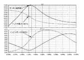
図2の(b)に示した差動駆動型の回路構成の基本的なマッチング回路におけるTx1,Tx2端子からみたインピーダンス特性の計算結果を図3に示す。 FIG. 3 shows the calculation result of the impedance characteristics viewed from the Tx1 and Tx2 terminals in the basic matching circuit having the differential drive type circuit configuration shown in FIG.
図3において、実線がインピーダンスZを示し、点線が位相θを示しており、θ=0になる点が共振点である。 In FIG. 3, the solid line indicates the impedance Z, the dotted line indicates the phase θ, and the point where θ = 0 is the resonance point.
周波数が低いときにはアンテナコイルL1に直列のコンデンサC4,C5の容量Csが支配的でインピーダンスZは減少し位相θはマイナスを示しているが、周波数が高くなる従ってアンテナコイルL1のインダクタンスの効果が大きくなり、インピーダンスZが大きくなり、位相θがプラスに転じる。この第1共振点での共振周波数は、抵抗が小さくなるためアンテナコイルL1に大きな電流を流すことができるので、R/Wモードとして使用される。When the frequency is low, the capacitance Cs of the capacitors C4 and C5 in series with the antenna coil L1 is dominant and the impedance Z is decreased and the phase θ is negative. However, since the frequency is high, the inductance effect of the antenna coil L1 is large. Thus, the impedance Z increases and the phase θ turns to a plus. Theresonance frequency at the first resonance point is used as the R / W mode because a large current can flow through the antenna coil L1 because the resistance is small.
図4にアンテナ電流最大値とインピーダンスZ(θ)=0とアンテナ電流(θ)=0を比較して示すように、アンテナ電流最大値は、インピーダンスZ(θ)=0、アンテナ電流(θ)=0と近い値を示すが、少しずれている。すなわち、共振アンテナは、ノイズ除去用のEMCフィルタや直列コンデンサC4,C5を含んだ回路となるので、コンデンサC1,C3のアンテナコイルL1で構成される並列共振回路のアンテナ電流(θ)=0やインピーダンスZ(θ)=0とは必ずしも一致しない。ただし、インピーダンスZ(θ)は、EMCフィルターや直列共振コンデンサなどの周辺回路部を含めて検出しているので、アンテナ電流(θ)=0よりもアンテナ電流最大値に近い値となっている。 As shown in FIG. 4 comparing the antenna current maximum value, impedance Z (θ) = 0 and antenna current (θ) = 0, the antenna current maximum value is impedance Z (θ) = 0, antenna current (θ). Although the value is close to 0, it is slightly shifted. That is, since the resonant antenna is a circuit including an EMC filter for noise removal and series capacitors C4 and C5, the antenna current (θ) = 0 of the parallel resonant circuit configured by the antenna coil L1 of the capacitors C1 and C3 The impedance Z (θ) = 0 does not necessarily match. However, since the impedance Z (θ) is detected including peripheral circuit portions such as an EMC filter and a series resonance capacitor, the impedance Z (θ) is closer to the antenna current maximum value than the antenna current (θ) = 0.
インピーダンスZ(θ)は、Tx1,Tx2端子の端子電圧Vと電流Iを測定することにより、Z=V/Iにて計算することができ、端子電圧Vが一定とすれば、インピーダンスZの位相θは、電流Iの位相θと一致するので、Tx端子の電流位相を検出することで共振点を検出することもできる。 The impedance Z (θ) can be calculated as Z = V / I by measuring the terminal voltage V and current I at the terminals Tx1 and Tx2, and if the terminal voltage V is constant, the phase of the impedance Z Since θ coincides with the phase θ of the current I, the resonance point can also be detected by detecting the current phase of the Tx terminal.
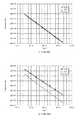
Tx端子のインピーダンスZ(θ)=0、電流I(θ)=0とアンテナ電流最大値の周波数を比較した結果を図5の(a),(b)に示す。図5の(a)は、アンテナ共振回路のQが30以上の高い場合の特性を示し、図5の(b)は、アンテナ共振回路のQが15の低い場合の特性を示している。図5の(a),(b)に示すように、アンテナ共振回路のQが30以上の高い場合は、インピーダンスZ(θ)=0、電流I(θ)=0とアンテナ電流最大値の周波数はよく一致しているが、アンテナ共振回路のQが15の低い場合はアンテナ電流との差が大きい。 FIGS. 5A and 5B show the results of comparing the impedance Z (θ) = 0, current I (θ) = 0 of the Tx terminal and the frequency of the antenna current maximum value. 5A shows the characteristics when the Q of the antenna resonance circuit is high of 30 or more, and FIG. 5B shows the characteristics when the Q of the antenna resonance circuit is as low as 15. FIG. As shown in FIGS. 5A and 5B, when the antenna resonance circuit has a high Q of 30 or more, impedance Z (θ) = 0, current I (θ) = 0, and the frequency of the antenna current maximum value. However, when Q of the antenna resonance circuit is as low as 15, the difference from the antenna current is large.
また、ICカードモードにおける共振周波数をピックアップコイルにより検出する場合のシミュレーション結果を図6に示す。図6における縦軸はインピーダンスである。ICカードモードでは、少ない電流で大きな電圧を誘起するために並列共振を利用してインピーダンスを高くしており、インピーダンス最大値を共振周波数としている。このICカードモードにおける共振周波数は、図3における第2共振点での共振周波数と一致しており、インピーダンスZ(θ)がプラスからマイナスへの遷移点である点で第1共振点での共振周波数とは違っている。FIG. 6 shows a simulation result when the resonance frequency in the IC card mode is detected by the pickup coil. The vertical axis in FIG. 6 is the impedance. In the IC card mode, in order to induce a large voltage with a small current, the impedance is increased by using parallel resonance, and the maximum impedance value is set as the resonance frequency. The resonance frequency in this IC card mode matchesthe resonance frequency at the second resonance point in FIG. 3, and the resonanceat the first resonance point is that the impedance Z (θ) is a transition point from plus to minus. It is different from frequency.
上記第1共振点での共振周波数と第2共振点での共振周波数は、インピーダンスZの位相θの変化の仕方で判別することができる。The firstresonance frequency at the resonance pointresonance frequency of the second resonance point can be determined in the manner of change of the phase θ of the impedance Z.
上記非接触通信デバイス100において、上記制御部23は、R/Wモードの調整モードの実行時に、上記発振部21の発振周波数を13.56MHzに設定し、上記デジタルアナログ変換部25から上記アンテナ共振回路10の制御端子を介して上記可変共振コンデンサVC1に印加するアナログ制御電圧信号Vcontを、上記位相検出部24で0位相が検出されるまで大きくしていき、0位相が検出されたときの印加電圧を第1共振点での共振周波数の制御電圧として記憶部26に記憶する。In the
なお、上記位相検出部24における0位相の検出は、位相検波で行うことができるが、位相がプラスからマイナスなった点を検出することにより、検出回路を簡略化することができる。 The detection of the zero phase in the
また、上記非接触通信デバイス100において、上記制御部23は、ICカードモードの調整モードの実行時には、上記発振部21の発振周波数を16.0MHzに設定し、上記デジタルアナログ変換部25から上記アンテナ共振回路10の制御端子を介して上記可変共振コンデンサVC1に印加するアナログ制御電圧信号Vcontを、上記位相検出部24で0位相が検出されるまで大きくしていき、上記出力部22の出力インピーダンスまたは出力電流の位相がマイナスからプラスに変わる点が検出されたときの印加電圧を第2共振点での共振周波数の制御電圧として記憶部26に記憶する。In the
上記制御部23は、調整モードにおいて、上記発振部21の発振周波数を制御し、上記アンテナ共振回路10における上記第1共振点での共振周波数と第2共振点での共振周波数を検出して、各制御電圧を記憶部26に記憶し、R/Wモード時に上記アンテナ共振回路10を上記第1共振点での共振周波数に制御し、ICカードモード時に上記アンテナ共振回路10を上記第2共振点での共振周波数に制御することができる。In the adjustment mode, the
上記非接触通信デバイス100では、制御部23により、動作モードに応じて発振部21の発振周波数を制御するとともに、位相検出部24により検出される出力部22の出力インピーダンスの位相または出力電流に基づいて、アンテナ共振回路10の共振周波数を制御するので、図2の(a)、(b)に示した基本的なマッチング回路におけるアンテナ電流位相検出用端子Imoniやモニタ抵抗R1を必要としない。 In the
ここで、上記制御部23は、R/Wモードの調整モードを実行する際に、アンテナ電流最大値とインピーダンスZ(θ)=0とのずれを考慮して設定周波数にオフセットを持たせるようにすることができる。このオフセット量は、アンテナ特性に依存するので、機器メーカが設定して記憶部26に記憶することができる。 Here, when executing the adjustment mode of the R / W mode, the
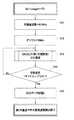
次に、上記非接触通信デバイス100におけるR/Wモードの調整モード(Self tuningモード1)での処理の具体的な手順を図7のフローチャートに示す。 Next, a specific procedure of processing in the R / W mode adjustment mode (Self tuning mode 1) in the
上記非接触通信デバイス100の制御部23は、Self tuningモード1に移行すると、最初に、記憶部26に記憶されている調整共振周波数とオフセットの値を読み出して発振部21にセットする(ステップS1,S2)。この例では、ステップS1においてR/Wモードの調整共振周波数として13.56MHzを発振部21にセットし、ステップS2において、共振アンテナに起因するオフセット量として0.1MHzを発振部21にセットする。 When the
これにより、発振部21は、13.56MHzにオフセット量0.1MHzを加えた13.66MHzで発振する。 Thereby, the
次に、制御部23は、上記デジタルアナログ変換部25から上記アンテナ共振回路10の制御端子を介して上記可変共振コンデンサVC1に印加するアナログ制御電圧信号Vcontを0Vから1ステップ毎に単位電圧ずつ増加させ(ステップS3)、上記位相検出部24で検出された位相がプラスからマイナスに変化したか否かを判定する(ステップS4)。 Next, the
上記制御部23は、上記ステップS4における判定結果が「No」、すなわち、上記位相検出部24で検出された位相がプラスからマイナスに変化していない場合には、上記ステップS3に戻って上記アナログ制御電圧信号Vcontを0Vから1ステップ毎に単位電圧ずつ増加させ、上記アンテナ共振回路10の共振周波数は順次高くしていく制御を、繰り返し行う。 When the determination result in Step S4 is “No”, that is, when the phase detected by the
そして、上記制御部23は、上記ステップS4における判定結果が「Yes」、すなわち、上記位相検出部24で検出された位相がプラスからマイナスに変化するまで、上記ステップS3とステップS4の処理を繰り返し行い、上記ステップS4における判定結果が「Yes」、すなわち、上記位相検出部24で検出された位相がプラスからマイナスに変化した時点で、上記デジタルアナログ変換部25から出力する上記アナログ制御電圧信号Vcontを0Vから1ステップ毎に単位電圧ずつ増加させたステップ数を最適調整値として記憶部26に記憶して(ステップS5)、Self tuningモード1による第1共振点での共振周波数の検出処理を終了する。Then, the
上記記憶部26に記憶した上記ステップ数は、上記位相検出部24で検出された位相がプラスからマイナスへの変化点、すなわち、上記アンテナ共振回路10の第1共振点での共振周波数に対応する上記可変共振コンデンサVC1の印加電圧の最適調整値になっている。The number of steps stored in the
また、上記非接触通信デバイス100におけるICカードモードの調整モード(Self tuningモード2)での処理の具体的な手順を図8のフローチャートに示す。 A specific procedure of processing in the IC card mode adjustment mode (Self tuning mode 2) in the
上記非接触通信デバイス100の制御部23は、Self tuningモード2に移行すると、最初に、記憶部26に記憶されている調整共振周波数とオフセットの値を読み出して発振部21にセットする(ステップS11,S12)。この例では、ステップS11においてICカードモードの調整共振周波数として16.0MHzを発振部21にセットし、ステップS2において、共振アンテナに起因するオフセット量として0MHzを発振部21にセットする。 When the
これにより、発振部21は、16.0MHzで発振する。 Thereby, the
次に、制御部23は、上記デジタルアナログ変換部25から上記アンテナ共振回路10の制御端子を介して上記可変共振コンデンサVC1に印加するアナログ制御電圧信号Vcontを0Vから1ステップ毎に単位電圧ずつ増加させ(ステップS13)、上記位相検出部24で検出された位相がマイナスからプラスに変化したか否かを判定する(ステップS14)。 Next, the
上記制御部23は、上記ステップS14における判定結果が「No」、すなわち、上記位相検出部24で検出された位相がマイナスからプラスに変化していない場合には、上記ステップS3に戻って上記アナログ制御電圧信号Vcontを第1の調整値から1ステップ毎に単位電圧ずつ増加させ、上記アンテナ共振回路10の共振周波数は順次高くしていく制御を、繰り返し行う。 When the determination result in step S14 is “No”, that is, when the phase detected by the
そして、上記制御部23は、上記ステップS4における判定結果が「Yes」、すなわち、上記位相検出部24で検出された位相がマイナスからプラスに変化するまで、上記ステップS13とステップS14の処理を繰り返し行い、上記ステップS14における判定結果が「Yes」、すなわち、上記位相検出部24で検出された位相がマイナスからプラスに変化した時点で、上記デジタルアナログ変換部25から出力する上記アナログ制御電圧信号Vcontを第1の調整値から1ステップ毎に単位電圧ずつ増加させたステップ数を最適調整値として記憶部26に記憶して(ステップS15)、Self tuningモード2による第2共振点での共振周波数の検出処理を終了する。
上記記憶部26に記憶した上記ステップ数は、上記位相検出部24で検出された位相がマイナスからプラスへの変化点、すなわち、上記アンテナ共振回路10の第2共振点での共振周波数に対応する上記可変共振コンデンサVC1の印加電圧の最適調整値になっている。Then, the
The number of steps stored in the
Self tuningモード2による第2共振点での共振周波数の検出処理フローでは、ステップS14において、Self tuningモード1による第1共振点での共振周波数の検出処理フローにおけるステップS4のように0Vからではなく、上記アナログ制御電圧信号Vcontを第1の調整値から1ステップ毎に単位電圧ずつ増加させるので、上記第1の調整値を最適値とすることにより調整時間を短縮することができる。Inthe resonance frequency detection process flow at the second resonance pointin the
ここで、Self tuningモード2による第2共振点での共振周波数の検出処理フローは、ステップS14において、上記位相検出部24で検出された位相がマイナスからプラスになる変化点を検出する処理を行う点以外は、Self tuningモード1による第1共振点での共振周波数の検出処理フローと同じになっている。 Here, the resonance frequency detection process flow at the second resonance point in the
このように、近距離無線通信(NFC:near field communication)システムなどに対応するR/W機能とICカード機能の両方を有する非接触通信デバイス100において、R/Wモードの調整モード(Self tuningモード1)での第1共振点での共振周波数の検出処理とICカードモードの調整モード(Self tuningモード2)での第2共振点での共振周波数の検出処理を同じ手法で行うことでき、通信用LSIで容易にSelf tuningを実現できる。As described above, in the
また、R/Wモードの調整モード(Self tuningモード1)で第1共振点での共振周波数の検出処理を行い、ICカードモードの調整モード(Self tuningモード2)で第2共振点での共振周波数の検出処理を行うものとして説明したが、上記非接触通信デバイス100では、R/Wモードの調整モードにおいて、制御部23により、発振部21の発振周波数を制御し、1回の共振周波数走査で、位相検出部24により検出される出力部22の出力インピーダンスまたは出力電流の位相がマイナスからプラスに変わるアンテナ共振回路10の第2共振点での共振周波数と、上記出力部22の出力インピーダンスまたは出力電流の位相がプラスからマイナスに変わる上記アンテナ共振回路10の第1共振点での共振周波数を検出して記憶部26に記憶することもできる。Further, performs detection processing of theresonance frequency of the first resonance point in R / W mode adjustment mode (Self tuning mode 1),the resonance at the second resonance point in the IC card mode adjustment mode (Self tuning mode 2)Although described as performingfrequency detection processing, in the
以上説明したように、上記非接触通信デバイス100では、制御部23により、動作モードに応じて発振部21の発振周波数を制御するとともに、位相検出部24により検出される出力部22の出力インピーダンスまたは出力電流の位相に基づいて、アンテナ共振回路10の共振周波数を制御するので、アンテナ電流位相検出用に信号線をアンテナから引き出すことなく、アンテナ端子及びLSI端子の増設や外付け抵抗によるコストアップや共振のQの低下や、不要輻射などのノイズの増加等の問題点がない。しかも、NFCシステムなどにおけるR/WモードとICカードモードにおける各共振周波数に対応することができる。 As described above, in the
10 アンテナ共振回路、11 直並列共振回路、20 アンテナ駆動部、21 発振部、22 出力部、22A,22B 差動増幅器、23 制御部、24 位相検出部、25 デジタルアナログ変換部、26 記憶部、100 非接触通信デバイス、L1 アンテナコイル、C1〜C7 コンデンサ、VC1 可変共振コンデンサ、L2、L3 コイル、12 EMCフィルタ、R1,R2 バイアス抵抗 DESCRIPTION OF
Claims (7)
Translated fromJapanese上記アンテナ共振回路に接続されるアンテナ駆動部とを備え、
上記アンテナ駆動部は、発振周波数が制御可能な発振部と、上記発振部により得られる高周波信号を上記アンテナ共振回路に供給する出力部と、上記発振部の発振周波数及び上記アンテナ共振回路のアンテナ共振周波数を制御する制御部と、上記出力部の出力インピーダンスまたは出力電流の位相を検出する位相検出部とを備え、
上記制御部により、動作モードに応じて上記発振部の発振周波数を制御するとともに、上記位相検出部により検出される上記出力部の出力インピーダンスまたは出力電流の位相に基づいて、上記アンテナ共振回路の共振周波数を制御することを特徴とする非接触通信デバイス。An antenna resonance circuit capable of controlling the resonance frequency of the antenna for electromagnetically communicating with the other party, and
An antenna drive unit connected to the antenna resonance circuit,
The antenna drive unit includes an oscillation unit whose oscillation frequency can be controlled, an output unit that supplies a high-frequency signal obtained by the oscillation unit to the antenna resonance circuit, an oscillation frequency of the oscillation unit, and an antenna resonance of the antenna resonance circuit A control unit that controls the frequency, and a phase detection unit that detects the phase of the output impedance or output current of the output unit,
The control unit controls the oscillation frequency of the oscillation unit according to the operation mode, and the resonance of the antenna resonance circuit is based on the output impedance or the phase of the output current detected by the phase detection unit. A non-contact communication device characterized by controlling a frequency.
上記制御部は、上記動作モードに応じた発振周波数において、上記アンテナ共振回路の共振周波数を上昇させるように制御することにより、上記位相検出部により検出される上記出力部の出力インピーダンスまたは出力電流の位相がマイナスからプラスに変わる点を第2共振点での共振周波数とし、上記出力部の出力インピーダンスまたは出力電流の位相がプラスからマイナスに変わる点を第1共振点での共振周波数とすることを特徴とする請求項1記載の非接触通信デバイス。The antenna resonance circuit is a series-parallel resonance circuit in which a capacitor is connected in series and parallel to an antenna coil,
The control unit performs control so as to increase the resonance frequency of the antenna resonance circuit at an oscillation frequency corresponding to the operation mode, whereby the output impedance or output current of the output unit detected by the phase detection unit is increased. The point where the phase changes from minus to plus is the resonance frequency at the second resonance point, and the point where the output impedance or output current phase of the output section changes from plus to minus is the resonance frequency at the first resonance point. The contactless communication device according to claim 1.
上記制御部により、動作モードに応じて上記発振部の発振周波数を制御するとともに、上記位相検出部により検出される上記出力部の出力インピーダンスまたは出力電流の位相に基づいて、上記アンテナ共振回路の共振周波数を制御することを特徴とするアンテナ共振周波数制御方法。The antenna drive unit is connected to an antenna resonance circuit capable of controlling the resonance frequency of the antenna for electromagnetically communicating with the other party, and the antenna drive unit has an oscillation frequency of a high-frequency signal supplied to the antenna resonance circuit. A controllable oscillation unit; an output unit that supplies a high-frequency signal obtained by the oscillation unit to the antenna resonance circuit; a control unit that controls the oscillation frequency of the oscillation unit and the antenna resonance frequency of the antenna resonance circuit; An antenna resonance frequency control method in a non-contact communication device comprising: a phase detection unit that detects an output impedance or an output current phase of an output unit;
The control unit controls the oscillation frequency of the oscillation unit according to the operation mode, and the resonance of the antenna resonance circuit is based on the output impedance or the phase of the output current detected by the phase detection unit. An antenna resonance frequency control method characterized by controlling a frequency.
R/Wモード時に上記アンテナ共振回路を上記第1共振点での共振周波数に制御し、
ICカードモード時に上記アンテナ共振回路を上記第2共振点での共振周波数に制御することを特徴とする請求項5記載のアンテナ共振周波数制御方法。In the adjustment mode, the antenna resonance circuit is controlled so as to increase the resonance frequency of the antenna resonance circuit, and the phase of the output impedance or output current of the output unit detected by the phase detection unit changes from minus to plus. The resonance frequencyat the secondresonance point and the resonance frequency at the firstresonance point of the antenna resonance circuit where the output impedance or output current phase of the output section changes from plus to minus are detected and stored in the storage means. ,
Controlling the antenna resonance circuit to the resonance frequency at the first resonance point in the R / W mode;
6. The antenna resonance frequency control method according to claim 5, wherein the antenna resonance circuit is controlled to a resonance frequency at the second resonance point in an IC card mode.
Priority Applications (5)
| Application Number | Priority Date | Filing Date | Title |
|---|---|---|---|
| JP2014003750AJP5883890B2 (en) | 2014-01-10 | 2014-01-10 | Non-contact communication device and antenna resonance frequency control method thereof |
| US15/110,257US20160329638A1 (en) | 2014-01-10 | 2015-01-07 | Non-contact communication device and antenna resonance frequency control method |
| PCT/JP2015/050216WO2015105116A1 (en) | 2014-01-10 | 2015-01-07 | Non-contact communication device and antenna resonance frequency control method |
| CN201580004103.8ACN105900349A (en) | 2014-01-10 | 2015-01-07 | Non-contact communication device and its antenna resonant frequency control method |
| TW104100709ATW201531950A (en) | 2014-01-10 | 2015-01-09 | Non-contact communication component and antenna antenna resonance frequency control method thereof |
Applications Claiming Priority (1)
| Application Number | Priority Date | Filing Date | Title |
|---|---|---|---|
| JP2014003750AJP5883890B2 (en) | 2014-01-10 | 2014-01-10 | Non-contact communication device and antenna resonance frequency control method thereof |
Publications (3)
| Publication Number | Publication Date |
|---|---|
| JP2015133602A JP2015133602A (en) | 2015-07-23 |
| JP2015133602A5 JP2015133602A5 (en) | 2015-10-01 |
| JP5883890B2true JP5883890B2 (en) | 2016-03-15 |
Family
ID=53523941
Family Applications (1)
| Application Number | Title | Priority Date | Filing Date |
|---|---|---|---|
| JP2014003750AExpired - Fee RelatedJP5883890B2 (en) | 2014-01-10 | 2014-01-10 | Non-contact communication device and antenna resonance frequency control method thereof |
Country Status (5)
| Country | Link |
|---|---|
| US (1) | US20160329638A1 (en) |
| JP (1) | JP5883890B2 (en) |
| CN (1) | CN105900349A (en) |
| TW (1) | TW201531950A (en) |
| WO (1) | WO2015105116A1 (en) |
Families Citing this family (13)
| Publication number | Priority date | Publication date | Assignee | Title |
|---|---|---|---|---|
| DE102014113910A1 (en)* | 2014-09-25 | 2016-03-31 | Huf Hülsbeck & Fürst Gmbh & Co. Kg | Antenna circuit for near-field antennas |
| US10055613B1 (en)* | 2017-02-06 | 2018-08-21 | Nxp B.V. | NFC reader with auto tuner |
| US10108825B2 (en) | 2017-03-22 | 2018-10-23 | Nxp B.V. | NFC reader with remote antenna |
| US10511347B2 (en)* | 2017-11-14 | 2019-12-17 | Nxp B.V. | Device detection in contactless communication systems |
| JP2019114069A (en)* | 2017-12-25 | 2019-07-11 | 日本電産サンキョー株式会社 | Card reader |
| DE102018124480B4 (en)* | 2018-10-04 | 2020-12-10 | Infineon Technologies Ag | COMMUNICATION DEVICE AND METHOD OF OPERATING AN ANTENNA TURN CIRCUIT |
| JP7396273B2 (en)* | 2018-10-24 | 2023-12-12 | ソニーグループ株式会社 | Cartridge memory and its control method, cartridge and recording/playback system |
| CN109756243B (en)* | 2018-12-27 | 2021-05-18 | 深圳市有方科技股份有限公司 | Antenna detection device and antenna detection method |
| JP7477346B2 (en)* | 2020-03-31 | 2024-05-01 | Tdk株式会社 | Wireless power transmission device and wireless power transmission system |
| JP7477347B2 (en) | 2020-03-31 | 2024-05-01 | Tdk株式会社 | Wireless power transmission device and wireless power transmission system |
| CN114427918B (en)* | 2020-10-29 | 2025-08-01 | 紫光同芯微电子有限公司 | Automatic temperature protection circuit of non-contact card chip |
| CN113255388B (en)* | 2021-06-30 | 2021-09-28 | 北京紫光微电子系统有限公司 | Card reader and card reading method without communication with NFC module of mobile phone |
| US11916619B2 (en)* | 2022-02-10 | 2024-02-27 | Semiconductor Components Industries, Llc | Auto-tuner for resonant circuit |
Family Cites Families (9)
| Publication number | Priority date | Publication date | Assignee | Title |
|---|---|---|---|---|
| US7310243B2 (en)* | 2004-06-10 | 2007-12-18 | International Business Machines Corporation | Method and components for implementing EMC shielded resonance damping |
| US7310245B2 (en)* | 2005-04-22 | 2007-12-18 | Noboru Ohbo | Electric power transmission device and electric power transmission method |
| US8219053B2 (en)* | 2007-10-19 | 2012-07-10 | Destron Fearing Corporation | Automatic tuning reader |
| JP5023965B2 (en)* | 2007-10-26 | 2012-09-12 | ソニー株式会社 | Reader / writer device and non-contact data carrier system |
| FR2947362A1 (en)* | 2009-06-25 | 2010-12-31 | St Microelectronics Sas | AUTHENTICATION OF A TERMINAL BY AN ELECTROMAGNETIC TRANSPONDER |
| JP5736991B2 (en)* | 2010-07-22 | 2015-06-17 | Tdk株式会社 | Wireless power supply apparatus and wireless power transmission system |
| JP5834655B2 (en)* | 2011-09-09 | 2015-12-24 | ソニー株式会社 | Transmission device, transmission / reception device, and integrated circuit |
| US9356474B2 (en)* | 2011-09-28 | 2016-05-31 | Tdk Corporation | Wireless power feeder and wireless power transmission system |
| WO2014207804A1 (en)* | 2013-06-24 | 2014-12-31 | 富士通株式会社 | Power transmission device and power transmission method |
- 2014
- 2014-01-10JPJP2014003750Apatent/JP5883890B2/ennot_activeExpired - Fee Related
- 2015
- 2015-01-07USUS15/110,257patent/US20160329638A1/ennot_activeAbandoned
- 2015-01-07WOPCT/JP2015/050216patent/WO2015105116A1/enactiveApplication Filing
- 2015-01-07CNCN201580004103.8Apatent/CN105900349A/enactivePending
- 2015-01-09TWTW104100709Apatent/TW201531950A/enunknown
Also Published As
| Publication number | Publication date |
|---|---|
| CN105900349A (en) | 2016-08-24 |
| US20160329638A1 (en) | 2016-11-10 |
| TW201531950A (en) | 2015-08-16 |
| JP2015133602A (en) | 2015-07-23 |
| WO2015105116A1 (en) | 2015-07-16 |
Similar Documents
| Publication | Publication Date | Title |
|---|---|---|
| JP5883890B2 (en) | Non-contact communication device and antenna resonance frequency control method thereof | |
| JP2015133602A5 (en) | ||
| CN106537801B (en) | Communication device, circuit, driving device, power supply device and tuning and discovery method | |
| CN106953650B (en) | NFC or RFID device RF detuning detection and driver output power regulation | |
| JP5640655B2 (en) | Portable communication device, reader / writer device, and resonance frequency adjusting method | |
| US20160112028A1 (en) | Automatic impedance adjustment | |
| US20190068248A1 (en) | Transmission Apparatus, Antenna Drive Apparatus, Tuning Method, and Program for Realizing Tuning Method | |
| JP6879847B2 (en) | High-resolution tuning of the phase of active load modulation in NFC systems and systems | |
| TWI520513B (en) | Controlling antenna characteristics of a near field communications (nfc) device | |
| CN109428631A (en) | System for using system information calibration phase | |
| EP3358751B1 (en) | Nfc reader with auto tuner | |
| CN108649989A (en) | Nfc reader with remote antenna | |
| US20120242456A1 (en) | Rfid module | |
| CN106549506B (en) | Tuning in a wireless power transmitter | |
| JP5996753B2 (en) | Discovery method and program thereof | |
| KR102408539B1 (en) | Crystal oscillator circuit | |
| JP2005063123A (en) | Non-contact type IC card reader / writer device, automatic adjustment method of antenna natural frequency, program | |
| JP2008109200A (en) | Communication device | |
| WO2011048728A1 (en) | Near field communication apparatus, and semiconductor integrated circuit for near field communication | |
| JP2014027513A (en) | Radio communication apparatus and method for correcting resonance frequency in radio communication apparatus | |
| JP6535510B2 (en) | Noncontact communication device, signal generation circuit, and noncontact communication method | |
| WO2016084338A1 (en) | Control method, non-contact communication device, non-contact feeder device, program, and drive circuit | |
| Dieng et al. | Study of adaptive tuning strategies for near field communication (nfc) transmitter module | |
| JP6699492B2 (en) | Wireless communication device | |
| Go et al. | Wireless power transfer system based on magnetic resonant coupling with directional coupler |
Legal Events
| Date | Code | Title | Description |
|---|---|---|---|
| A521 | Request for written amendment filed | Free format text:JAPANESE INTERMEDIATE CODE: A523 Effective date:20150818 | |
| A621 | Written request for application examination | Free format text:JAPANESE INTERMEDIATE CODE: A621 Effective date:20150818 | |
| A871 | Explanation of circumstances concerning accelerated examination | Free format text:JAPANESE INTERMEDIATE CODE: A871 Effective date:20150818 | |
| A975 | Report on accelerated examination | Free format text:JAPANESE INTERMEDIATE CODE: A971005 Effective date:20150828 | |
| A131 | Notification of reasons for refusal | Free format text:JAPANESE INTERMEDIATE CODE: A131 Effective date:20150901 | |
| A521 | Request for written amendment filed | Free format text:JAPANESE INTERMEDIATE CODE: A523 Effective date:20151102 | |
| RD03 | Notification of appointment of power of attorney | Free format text:JAPANESE INTERMEDIATE CODE: A7423 Effective date:20151113 | |
| A131 | Notification of reasons for refusal | Free format text:JAPANESE INTERMEDIATE CODE: A131 Effective date:20151208 | |
| A521 | Request for written amendment filed | Free format text:JAPANESE INTERMEDIATE CODE: A523 Effective date:20160114 | |
| TRDD | Decision of grant or rejection written | ||
| A01 | Written decision to grant a patent or to grant a registration (utility model) | Free format text:JAPANESE INTERMEDIATE CODE: A01 Effective date:20160202 | |
| A61 | First payment of annual fees (during grant procedure) | Free format text:JAPANESE INTERMEDIATE CODE: A61 Effective date:20160208 | |
| R150 | Certificate of patent or registration of utility model | Ref document number:5883890 Country of ref document:JP Free format text:JAPANESE INTERMEDIATE CODE: R150 | |
| LAPS | Cancellation because of no payment of annual fees |