JP5881956B2 - Substrate processing apparatus, semiconductor device manufacturing method, and wafer holder - Google Patents
Substrate processing apparatus, semiconductor device manufacturing method, and wafer holderDownload PDFInfo
- Publication number
- JP5881956B2 JP5881956B2JP2011041214AJP2011041214AJP5881956B2JP 5881956 B2JP5881956 B2JP 5881956B2JP 2011041214 AJP2011041214 AJP 2011041214AJP 2011041214 AJP2011041214 AJP 2011041214AJP 5881956 B2JP5881956 B2JP 5881956B2
- Authority
- JP
- Japan
- Prior art keywords
- substrate
- holder
- wafer
- gas
- main body
- Prior art date
- Legal status (The legal status is an assumption and is not a legal conclusion. Google has not performed a legal analysis and makes no representation as to the accuracy of the status listed.)
- Active
Links
Images


Classifications
- H—ELECTRICITY
- H01—ELECTRIC ELEMENTS
- H01L—SEMICONDUCTOR DEVICES NOT COVERED BY CLASS H10
- H01L21/00—Processes or apparatus adapted for the manufacture or treatment of semiconductor or solid state devices or of parts thereof
- H01L21/67—Apparatus specially adapted for handling semiconductor or electric solid state devices during manufacture or treatment thereof; Apparatus specially adapted for handling wafers during manufacture or treatment of semiconductor or electric solid state devices or components ; Apparatus not specifically provided for elsewhere
- H01L21/677—Apparatus specially adapted for handling semiconductor or electric solid state devices during manufacture or treatment thereof; Apparatus specially adapted for handling wafers during manufacture or treatment of semiconductor or electric solid state devices or components ; Apparatus not specifically provided for elsewhere for conveying, e.g. between different workstations
- H01L21/67739—Apparatus specially adapted for handling semiconductor or electric solid state devices during manufacture or treatment thereof; Apparatus specially adapted for handling wafers during manufacture or treatment of semiconductor or electric solid state devices or components ; Apparatus not specifically provided for elsewhere for conveying, e.g. between different workstations into and out of processing chamber
- H01L21/67757—Apparatus specially adapted for handling semiconductor or electric solid state devices during manufacture or treatment thereof; Apparatus specially adapted for handling wafers during manufacture or treatment of semiconductor or electric solid state devices or components ; Apparatus not specifically provided for elsewhere for conveying, e.g. between different workstations into and out of processing chamber vertical transfer of a batch of workpieces
- H—ELECTRICITY
- H01—ELECTRIC ELEMENTS
- H01L—SEMICONDUCTOR DEVICES NOT COVERED BY CLASS H10
- H01L21/00—Processes or apparatus adapted for the manufacture or treatment of semiconductor or solid state devices or of parts thereof
- H01L21/67—Apparatus specially adapted for handling semiconductor or electric solid state devices during manufacture or treatment thereof; Apparatus specially adapted for handling wafers during manufacture or treatment of semiconductor or electric solid state devices or components ; Apparatus not specifically provided for elsewhere
- H01L21/673—Apparatus specially adapted for handling semiconductor or electric solid state devices during manufacture or treatment thereof; Apparatus specially adapted for handling wafers during manufacture or treatment of semiconductor or electric solid state devices or components ; Apparatus not specifically provided for elsewhere using specially adapted carriers or holders; Fixing the workpieces on such carriers or holders
- H01L21/67303—Vertical boat type carrier whereby the substrates are horizontally supported, e.g. comprising rod-shaped elements
- H01L21/67309—Vertical boat type carrier whereby the substrates are horizontally supported, e.g. comprising rod-shaped elements characterized by the substrate support
Landscapes
- Engineering & Computer Science (AREA)
- Physics & Mathematics (AREA)
- Condensed Matter Physics & Semiconductors (AREA)
- General Physics & Mathematics (AREA)
- Manufacturing & Machinery (AREA)
- Computer Hardware Design (AREA)
- Microelectronics & Electronic Packaging (AREA)
- Power Engineering (AREA)
- Container, Conveyance, Adherence, Positioning, Of Wafer (AREA)
- Chemical Vapour Deposition (AREA)
- Furnace Charging Or Discharging (AREA)
Description
Translated fromJapanese本発明は、複数積層された基板を処理する基板処理装置および基板若しくは半導体デバイスの製造方法に係り、特に、炭化ケイ素(SiC)エピタキシャル膜を基板上に成膜する基板処理装置に関するものである。 The present invention relates to a substrate processing apparatus for processing a plurality of stacked substrates and a method for manufacturing a substrate or a semiconductor device, and more particularly to a substrate processing apparatus for forming a silicon carbide (SiC) epitaxial film on a substrate.
炭化ケイ素(SiC)は、ケイ素(Si)に比して、絶縁耐圧や熱伝導性が高いこと等から、特にパワーデバイス用素子材料として注目されている。その一方でSiCは、不純物拡散係数が小さいこと等から、Siに比して結晶基板や半導体装置(半導体デバイス)の製造が難しいことが知られている。例えば、Siのエピタキシャル成膜温度が900℃〜1200℃程度であるのに対し、SiCのエピタキシャル成膜温度は1500℃〜1800℃程度となっており、装置の耐熱構造や材料の分解抑制等に技術的な工夫が必要となる。 Silicon carbide (SiC) is particularly attracting attention as an element material for power devices because it has higher withstand voltage and higher thermal conductivity than silicon (Si). On the other hand, it is known that SiC is difficult to manufacture a crystal substrate and a semiconductor device (semiconductor device) as compared with Si because of a small impurity diffusion coefficient. For example, the epitaxial film formation temperature of Si is about 900 ° C. to 1200 ° C., whereas the epitaxial film formation temperature of SiC is about 1500 ° C. to 1800 ° C. Need to be creative.
複数の基板を効率的に処理し得るバッチ式の基板処理装置として、例えば、縦方向に複数の基板を積層するよう保持するボートを備えた、所謂バッチ式縦型基板処理装置が知られている。このバッチ式縦型基板処理装置は、複数の基板を積層するよう保持したボートを処理炉内に搬送し、その後、処理炉内を所定温度に昇温させつつ、処理炉内に設けたガスノズルから各基板に向けて反応ガスを供給する。これにより、各基板の成膜面が反応ガスに曝されて、各基板を一度に効率良く成膜処理することができる。 As a batch-type substrate processing apparatus capable of efficiently processing a plurality of substrates, for example, a so-called batch-type vertical substrate processing apparatus having a boat that holds a plurality of substrates stacked in the vertical direction is known. . This batch type vertical substrate processing apparatus transports a boat holding a plurality of substrates to be stacked in a processing furnace, and then raises the temperature in the processing furnace to a predetermined temperature while using a gas nozzle provided in the processing furnace. A reactive gas is supplied toward each substrate. Thereby, the deposition surface of each substrate is exposed to the reaction gas, and each substrate can be efficiently deposited at once.
このような所謂バッチ式縦型基板処理装置としては、例えば、特許文献1および特許文献2に記載された技術が知られている。 As such a so-called batch type vertical substrate processing apparatus, for example, techniques described in
特許文献1に記載された基板処理装置は、複数のウェーハ(基板)を積層して保持するボートを備え、当該ボートを形成する複数の支柱には、円環状の石英製のホルダプレートが水平姿勢となるよう多段に溶接されている。また、各ホルダプレートの径方向内側(内周側)にはそれぞれ合計3個の爪が溶接等により固着され、各爪はウェーハを水平姿勢で保持するようになっている。ホルダプレートの径方向外側には、反応ガス導入管(ガスノズル)が設けられ、当該反応ガス導入管から供給される反応ガスは、径方向外側から各支柱がある部分を通過して各ウェーハに到達する。各支柱は反応ガスに曝されるため、各支柱においても成膜される。つまり、各支柱は反応ガスを消費するので、各支柱周辺の反応ガスの成膜成分濃度は低下した状態となる。これに対し、特許文献1に記載された基板処理装置においては、各支柱と各ウェーハとの間の距離を遠ざけているので、各ウェーハの成膜面に略一定濃度の反応ガスを供給できるようにし、成膜精度に悪影響が出るのを抑えている。 The substrate processing apparatus described in
特許文献2に記載された基板処理装置は、ボートを形成する複数の支柱にそれぞれ円柱状のウェハ支持部を溶接等により固着し、各ウェハ支持部によってウェハ(基板)を支持するようにしている。そして、上述のような各支柱による反応ガスの消費を考慮して、各支柱に対応する部分にそれぞれ切欠きを備えたリング状プレートを、各支柱に溶接等により固着している。これにより、各切欠き部分の各支柱および各切欠き部分以外のリング状プレートの部分が反応ガスを消費し、ひいては各ウェーハの成膜面に略一定濃度の反応ガスを供給することができ、成膜精度に悪影響が出るのを抑えている。 In the substrate processing apparatus described in
しかしながら、上述した特許文献1および特許文献2に記載された基板処理装置によれば、複数の部材、つまりホルダプレート,ウェハ支持部およびリング状プレートを、支柱(ボート柱)に溶接等により固着し、これにより石英製のボートを形成している。そのため、当該石英製のボートをそのまま1000℃を超える高温下で使用すると溶解する等の問題が生じ得る。そこで、SiCのエピタキシャル成膜温度(1500℃〜1800℃程度)に対応し得る耐熱構造のボートを別途開発する必要があった。SiC等の耐熱性に優れた材料を用いて、従前のような複数の部材を固着してなるボートを形成することも考えられるが、SiC等の材料は耐熱性に優れる分、溶接等による固着が困難である。つまり、単純に耐熱性に優れた材料に切り替えて、従前のようなボートを形成することはできず、ボートに対するウェーハの積層構造を他の観点からも見直す必要が生じていた。 However, according to the substrate processing apparatus described in
本発明の目的は、成膜精度に悪影響を及ぼさず、かつ高温に耐え得るウェーハの積層構造を有する基板処理装置を提供することにある。 An object of the present invention is to provide a substrate processing apparatus having a laminated structure of a wafer that does not adversely affect film forming accuracy and can withstand high temperatures.
本発明の前記ならびにその他の目的と新規な特徴は、本明細書の記述および添付図面から明らかになるであろう。 The above and other objects and novel features of the present invention will be apparent from the description of this specification and the accompanying drawings.
本願において開示される発明のうち、代表的なものの概要を簡単に説明すれば、次のとおりである。 Of the inventions disclosed in the present application, the outline of typical ones will be briefly described as follows.
すなわち、本発明に係る基板処理装置は、基板を処理する反応容器と、前記反応容器内に設けられ、前記基板に反応ガスを供給するガスノズルと、前記基板を内周側で保持し、前記基板の外径寸法よりも大きい外径寸法のウェーハホルダと、前記ウェーハホルダを取り外せるようにその外周側を保持するホルダ保持部を有する複数のホルダ保持柱とを備え、前記ウェーハホルダは、前記ウェーハホルダを前記ホルダ保持部に保持させた状態のもとで、前記ウェーハホルダの前記ホルダ保持部側に設けられる本体部と、前記基板を中心に前記ウェーハホルダの前記ホルダ保持部側とは反対側に設けられ、前記本体部よりも薄肉とされた薄肉部とを有し、前記ホルダ保持柱の幅寸法で、前記ウェーハホルダの径方向外側から前記基板の中心まで延ばした第1仮想長方形における前記本体部の表面積を、前記本体部に連通穴を設けることで、前記第1仮想長方形を前記基板の中心を中心として、前記薄肉部まで回転させた第3仮想長方形における前記薄肉部の表面積よりも小さくし、前記第3仮想長方形における前記薄肉部の重量を、薄く加工することで、前記第1仮想長方形における前記本体部の重量と略同じ重量にしている。That is, a substrate processing apparatus according to the present invention includes a reaction vessel that processes a substrate, a gas nozzle that is provided in the reaction vessel and supplies a reaction gas to the substrate, and holds the substrate on an inner peripheral side. A wafer holder having an outer diameter larger than the outer diameter of the wafer holder, and a plurality of holder holding pillars having a holder holding portion for holding the outer periphery of the wafer holder so that the wafer holder can be removed. In the state where the holder is held by the holder holding portion, the main body provided on the holder holding portion side of the wafer holder, and on the opposite side of the wafer holder from the holder holding portion side around the substrate provided, and a thin portion which is thinner than the main body portion, a width dimension of the holder holding column, extendingfrom a radially outer side of the wafer holder to the center of the substrate The surface area of the main body portion in the first virtual rectangle is provided in the third virtual rectangle in which the first virtual rectangle is rotated to the thin-walled portion around the center of the substrate by providing a communication hole in the main body portion. The surface area of the thin wall portion is made smaller, and the weight of the thin wall portion in the third virtual rectangle is processed to be substantially the same as the weight of the main body portion in the first virtual rectangle.
本願において開示される発明のうち、代表的なものによって得られる効果を簡単に説明すれば以下の通りである。 The effects obtained by typical ones of the inventions disclosed in the present application will be briefly described as follows.
すなわち、成膜精度に悪影響を及ぼさず、かつ高温に耐え得るウェーハの積層構造を得ることができる。 That is, it is possible to obtain a laminated structure of a wafer that does not adversely affect the film forming accuracy and can withstand high temperatures.
[第1実施の形態]
以下、本発明の第1実施の形態について、図面を参照しつつ詳細に説明する。以下の実施の形態では、基板処理装置の一例であるSiCエピタキシャル成長装置において、高さ方向(縦方向)にSiCウェーハを積層する、所謂バッチ式縦型SiCエピタキシャル成長装置を挙げている。これにより、一度に処理できるSiCウェーハの数を増やしてスループット(製造効率)を向上させている。[First Embodiment]
Hereinafter, a first embodiment of the present invention will be described in detail with reference to the drawings. In the following embodiments, a so-called batch type vertical SiC epitaxial growth apparatus is described in which SiC wafers are stacked in the height direction (vertical direction) in a SiC epitaxial growth apparatus which is an example of a substrate processing apparatus. As a result, the number of SiC wafers that can be processed at one time is increased to improve throughput (manufacturing efficiency).
<全体の構成>
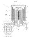
図1は本発明に係る基板処理装置の概要を示す斜視図であり、まず、図1を用いて、本発明の一実施の形態におけるSiCエピタキシャル膜を成膜する基板処理装置、および、半導体デバイスの製造工程の一つであるSiCエピタキシャル膜を成膜する基板の製造方法について説明する。<Overall configuration>
FIG. 1 is a perspective view showing an outline of a substrate processing apparatus according to the present invention. First, referring to FIG. 1, a substrate processing apparatus for forming a SiC epitaxial film according to an embodiment of the present invention, and a semiconductor device A method for manufacturing a substrate on which a SiC epitaxial film is formed will be described.
基板処理装置(成膜装置)としての半導体製造装置10は、バッチ式縦型熱処理装置であり、種々の機能を備えた複数の装置を収容する筐体12を有している。この半導体製造装置10では、例えば、SiC等で構成された基板としてのウェーハ14を収納する基板収容器として、ポッド(フープ)16をウェーハキャリアとして使用している。 A
筐体12の正面側には、ポッドステージ18が設けられ、当該ポッドステージ18上にポッド16が搬送されるようになっている。ポッド16には、例えば、25枚のウェーハ14が収納され、蓋16aが閉じられた状態(密閉状態)のもとで、ポッドステージ18上にセットされる。 A
筐体12の正面側で、かつポッドステージ18の背面側には、当該ポッドステージ18と対向するようにしてポッド搬送装置20が設けられている。また、ポッド搬送装置20の近傍でかつ背面側には、複数段(図示では3段)のポッド収納棚22,ポッドオープナ24および基板枚数検知器26が設けられている。各ポッド収納棚22は、ポッドオープナ24および基板枚数検知器26の上方側に設けられ、ポッド16を複数個搭載(図示では5個)し、その状態を保持するよう構成されている。ポッド搬送装置20は、ポッドステージ18,各ポッド収納棚22およびポッドオープナ24間で、次々とポッド16を搬送するようになっている。ポッドオープナ24は、ポッド16の蓋16aを開けるもので、基板枚数検知器26は、ポッドオープナ24に隣接して設けられ、蓋16aが開けられた状態のもとでポッド16内のウェーハ14の枚数を検知するものである。 A
筐体12の内部には、その他に、基板移載機28,基板保持具としてのボート30が設けられている。基板移載機28は、例えば、5本のアーム(ツイーザ)32を備え、各アーム32は、図示しない駆動手段により昇降可能かつ回転可能な構造となっており、ポッド16から5枚のウェーハ14を一度に取り出せるようになっている。そして、各アーム32を正面側から背面側に反転移動させることで、ポッドオープナ24の位置にあるポッド16からボート30に向けて、ウェーハ14を5枚ずつ搬送することができる。 In addition, a
筐体12内の背面側でかつ上方側には、処理炉40が設けられている。処理炉40の内部には、複数枚のウェーハ14を装填したボート30が搬入され、これにより、複数積層したウェーハ14を一度に熱処理(バッチ処理)できるようになっている。 A
<処理炉の構成>
図2は処理炉の内部構造を示す断面図を、図3は処理炉周辺の構造を示す断面図を、図4は基板処理装置の制御系統を説明するブロック図を、図5はボートの詳細構造を示す斜視図を、図6はウェーハをウェーハホルダに保持させた状態を示す断面図を、図7はウェーハおよびウェーハホルダを示す斜視図を、図8はウェーハホルダにおける反応ガスの消費部分を説明する説明図をそれぞれ表している。次に、これらの図2〜図8を用いて、SiCエピタキシャル膜を成膜する半導体製造装置10の処理炉40について説明する。<Processing furnace configuration>
2 is a cross-sectional view showing the internal structure of the processing furnace, FIG. 3 is a cross-sectional view showing the structure around the processing furnace, FIG. 4 is a block diagram for explaining the control system of the substrate processing apparatus, and FIG. FIG. 6 is a sectional view showing a state where the wafer is held by the wafer holder, FIG. 7 is a perspective view showing the wafer and the wafer holder, and FIG. 8 is a reaction gas consumption portion in the wafer holder. Each explanatory diagram to be described is shown. Next, the
処理炉40は、円筒形状の反応室44を形成する反応管42を備えている。反応管42は、石英またはSiC等の耐熱性材料からなり、上方側が閉塞され下方側が開口した有底筒状に形成されている。反応管42内の反応室44には、ボート30が収納されるようになっている。ここで、ボート30は、ウェーハホルダ100(図6〜図8参照)に搭載されたウェーハ14を、水平姿勢でかつ互いに中心を揃えて整列させ、縦方向に複数積層した状態で保持するようになっている。なお、ボート30の下方側には、例えば、石英やSiC等の耐熱性材料により円柱形状に形成された断熱部材としてのボート断熱部34が設けられ、加熱体48からの熱が、処理炉40の下方側に伝達し難くなっている。 The
反応管42の開口側(図中下方側)には、反応管42と同心円状にマニホールド36が配設されている。マニホールド36は、例えば、ステンレス材料等からなり、上方側および下方側が開口した円筒形状に形成されている。マニホールド36は反応管42を支持し、マニホールド36と反応管42との間には、シール部材としてのOリング(図示せず)が設けられている。これにより、反応管42およびマニホールド36の内部に充填された反応ガスが外部に漏洩するのを防止している。 A manifold 36 is disposed concentrically with the
マニホールド36は、その下方側に設けられた保持体(図示せず)に支持されており、これにより反応管42は、地面(図示せず)に対して垂直に据え付けられた状態となっている。ここで、反応管42およびマニホールド36により、反応容器を形成している。 The manifold 36 is supported by a holding body (not shown) provided on the lower side thereof, whereby the
処理炉40は、加熱体48と誘導コイル50とを備えている。加熱体48は反応室44内に設けられ、上方側が閉塞されて下方側が開口された有底筒状に形成されている。これにより、加熱体48内に供給される反応ガスを封止でき、かつ反応室44の上方側への放熱を抑制できる。加熱体48は、少なくとも複数積層されたウェーハ14の積層領域を囲むように設けられ、磁場発生部として機能する誘導コイル50により誘導加熱されるようになっている。 The
誘導コイル50は、円筒形状の支持部材51の内周側に螺旋状に固定され、当該誘導コイル50は外部電源(図示せず)により通電される。そして、誘導コイル50を通電することで当該誘導コイル50は磁場を発生し、ひいては加熱体48が誘導加熱される。このように加熱体48を誘導加熱により発熱させることで、反応室44内が加熱されるようになっている。 The
加熱体48の近傍には、反応室44内の温度を検出する温度検出体としての温度センサ(図示せず)が設けられており、当該温度センサおよび誘導コイル50は、コントローラ152の温度制御部52(図4参照)と電気的に接続されている。温度制御部52は、温度センサにより検出された温度情報に基づいて、反応室44内の温度が所望の温度分布となるよう、誘導コイル50への通電具合を所定のタイミングで調節(制御)するようになっている。 In the vicinity of the
反応管42と加熱体48との間には、例えば、誘導加熱され難いカーボンフェルト等で形成された断熱材54が設けられている。断熱材54は、側壁部54aと蓋部54bとを備え、反応管42および加熱体48と同様に、上方側が閉塞され下方側が開口された有底筒状に形成されている。このように、断熱材54を設けることで加熱体48からの輻射熱の伝達を遮断し、反応管42あるいは反応管42の外部が加熱されるのを抑制している。なお、側壁部54aおよび蓋部54bは、一体成形または別部材で構成することができる。 Between the
誘導コイル50の外周側には、反応室44内の熱が外部に伝達されるのを抑制するために、例えば、水冷構造の外側断熱壁55が設けられている。外側断熱壁55は円筒形状に形成され、反応室44(支持部材51)を包囲するよう配置されている。さらに、外側断熱壁55の外周側には、誘導コイル50を通電することで発生する磁場が、外部に漏洩するのを防止するための磁気シール58が設けられている。磁気シール58においても、上方側が閉塞され下方側が開口された有底筒状に形成されている。 For example, an outer
加熱体48と各ウェーハ14との間には、少なくともSi(シリコン)原子含有ガス,Cl(塩素)原子含有ガス,C(炭素)原子含有ガスおよび還元ガスを供給する複数の第1ガス供給口60を備えた第1ガス供給ノズル(ガスノズル)61が設けられている。また、加熱体48と各ウェーハ14との間で、第1ガス供給ノズル61の対向位置には、第1ガス供給ノズル61から供給された反応ガスを外部に排気する第1ガス排気口62が設けられている。さらに、反応管42と断熱材54の間には、第2ガス供給口64を備えた第2ガス供給ノズル65と、その対向位置には、第2ガス排気口66が設けられている。以下、それぞれのノズルについて説明する。 A plurality of first gas supply ports for supplying at least a Si (silicon) atom-containing gas, a Cl (chlorine) atom-containing gas, a C (carbon) atom-containing gas, and a reducing gas between the
第1ガス供給ノズル61は、例えば、カーボングラファイト等で中空パイプ状に形成され、その先端側は加熱体48の上方側に延在しており、第1ガス供給ノズル61の各第1ガス供給口60は各ウェーハ14の側面に向けられている。第1ガス供給ノズル61の基端側は、マニホールド36を貫通しつつ、当該マニホールド36に溶接等により固定されている。第1ガス供給ノズル61は、少なくとも、Si原子含有ガスとして例えばモノシラン(SiH4)ガス、Cl原子含有ガスとして例えば塩化水素(HCl)ガス、C原子含有ガスとして例えばプロパン(C3H8)ガス、還元ガスとして例えば水素(H2)ガスとをそれぞれ混合した状態とし、この反応ガスを各ウェーハ14に向けて供給するようになっている。The first
第1ガス供給ノズル61は、第1ガスライン68に接続されている。第1ガスライン68は、流量制御器(流量制御手段)としての各MFC(マスフローコントローラ)72a,72b,72c,72dおよび各バルブ74a,74b,74c,74dを介して、第1ガス源70a,第2ガス源70b,第3ガス源70c,第4ガス源70dに接続されている。なお、各ガス源70a〜70dには、例えば、SiH4ガス,HClガス,C3H8ガス,H2ガスがそれぞれ充填されている。The first
この構成により、例えば、SiH4ガス,HClガス,C3H8ガス,H2ガスのそれぞれの供給流量,濃度,分圧等を制御することができる。各バルブ74a〜74dおよび各MFC72a〜72dは、コントローラ152のガス流量制御部78(図4参照)に電気的に接続されている。ガス流量制御部78は、供給すべきそれぞれの反応ガスの流量を所定流量とするよう、所定のタイミングで制御するようになっている。ここで、SiH4ガス(成膜ガス),HClガス(エッチングガス),C3H8ガス(成膜ガス),H2ガス(還元ガス)をそれぞれ供給する各ガス源70a〜70d,各バルブ74a〜74d,各MFC72a〜72d,第1ガスライン68,第1ガス供給ノズル61および各第1ガス供給口60によって、第1ガス供給系を構成している。With this configuration, for example, the supply flow rate, concentration, partial pressure, and the like of SiH4 gas, HCl gas, C3 H8 gas, and H2 gas can be controlled. The
なお、上述においては、第1ガス供給ノズル61の各第1ガス供給口60から、少なくとも、Si原子含有ガス,Cl原子含有ガス,C原子含有ガスおよび還元ガスを供給するようにしたが、これに限らず、それぞれの反応ガスに対応させて個別にガス供給ノズルを設けても良い。この場合、各反応ガスは反応室44内で混合されることになる。また、例えば2つのガス供給ノズルを設けて、上記4種類の反応ガスのうちの2種類を任意の組み合わせで混合させておき、各ウェーハ14に向けて供給するようにしても良い。 In the above description, at least the Si atom-containing gas, the Cl atom-containing gas, the C atom-containing gas, and the reducing gas are supplied from the first
また、上述においては、Cl原子含有ガスとしてHClガスを用いた場合を例示したが、これに限らず、塩素(Cl2)ガス等を用いても良い。In the above description, the HCl gas is used as the Cl atom-containing gas. However, the present invention is not limited to this, and chlorine (Cl2 ) gas or the like may be used.
さらに、上述においては、Si原子含有ガスとCl原子含有ガスとを第1ガスライン68内で混合しておき、この混合した反応ガスを各第1ガス供給口60からウェーハ14に供給するようにしたが、これに限らず、Si原子とCl原子とを含有するガスである、例えばテトラクロロシラン(SiCl4)ガス,トリクロロシラン(SiHCl3)ガス,ジクロロシラン(SiH2Cl2)ガス等を供給するようにしても良い。Furthermore, in the above description, the Si atom-containing gas and the Cl atom-containing gas are mixed in the
また、上述においては、C原子含有ガスとしてC3H8ガスを用いた場合を例示したが、これに限らず、エチレン(C2H4)ガス,アセチレン(C2H2)ガス等を用いても良い。Further, in the above description, a case has been exemplified using aC 3H 8 gas as a C atom-containing gas is not limited thereto,
さらには、第1ガス供給ノズル61内でドーパントガスを混合させておき、各第1ガス供給口60からドーパントガスを含有する反応ガスを供給するようにしても良い。また、当該ドーパントガスを供給するための専用のガス供給ノズルを別途設け、当該ガス供給ノズルからドーパントガスを反応室44内に供給するようにしても良い。 Furthermore, the dopant gas may be mixed in the first
加熱体48と各ウェーハ14との間で第1ガス供給ノズル61と対向する第1ガス排気口62には、マニホールド36を貫通して当該マニホールド36に溶接等により固定されたガス排気管76が接続されている。これにより、反応室44内に供給された反応ガスは、第1ガス排気口62およびガス排気管76を介して、半導体製造装置10の外部に排出される。 A
このように、各第1ガス供給口60から反応室44内に、少なくとも、Si原子含有ガス,Cl原子含有ガス,C原子含有ガスおよび還元ガスを供給するようにし、各第1ガス供給口60から供給された反応ガスを、ボート30に積層された各ウェーハ14に対して側面方向から平行に流し、その後、反応ガスは第1ガス排気口62に向かう。これにより、各ウェーハ14の成膜面全体を、効率的かつ均一に反応ガスに曝すことができる。 As described above, at least the Si atom-containing gas, the Cl atom-containing gas, the C atom-containing gas, and the reducing gas are supplied from the first
ここで、好ましくは、反応室44の内部における加熱体48と各ウェーハ14との間で、かつ第1ガス供給ノズル61と第1ガス排気口62との間に、反応ガスの流れ方向を各ウェーハ14に向けるための構造物(図示せず)を設けると良い。この構造物の材料としては、好ましくは断熱材またはカーボングラファイト等を用いることで、耐熱性の向上やパーティクル発生の抑制を図ることができる。これにより、各第1ガス供給口60から供給される反応ガスを、より各ウェーハ14の成膜面全体に行き渡るようにすることができ、各ウェーハ14を効率的かつ均一に反応ガスに曝すことができる。ひいては各ウェーハ14上に成膜されるSiCエピタキシャル膜の膜厚均一性(成膜精度)を向上させることができる。 Here, preferably, the flow direction of the reaction gas is changed between the
反応管42と断熱材54との間に配置された第2ガス供給ノズル65の基端側は、マニホールド36を貫通して当該マニホールド36に溶接等により固定されている。第2ガス供給ノズル65は、第2ガスライン69に接続され、当該第2ガスライン69は、MFC72eおよびバルブ74eを介して、第5ガス源70eに接続されている。なお、第5ガス源70eには、例えば不活性ガスとして、希ガスのAr(アルゴン)ガスが充填されている。これにより、SiCエピタキシャル膜の成長に寄与する反応ガスが、反応管42と断熱材54との間に進入するのを防止し、反応管42の内壁や断熱材54の外壁に不要な生成物が付着するのを抑制できる。なお、バルブ74eおよびMFC72eにおいても、コントローラ152のガス流量制御部78(図4参照)に電気的に接続されている。 The proximal end side of the second
反応管42と断熱材54との間で、第2ガス供給ノズル65との対向部位には、第2ガス排気口66が設けられている。第2ガス排気口66においても、第1ガス排気口62と同様にガス排気管76に接続されている。ガス排気管76の下流側には、圧力検出器としての圧力センサ(図示せず)および圧力調整器としてのAPC(Auto Pressure Controller)バルブ79を介して、真空ポンプ等の真空排気装置80が接続されている。 A second
圧力センサおよびAPCバルブ79には、コントローラ152の圧力制御部98(図4参照)が電気的に接続されている。圧力制御部98は、圧力センサにより検出された圧力に基づき、所定のタイミングでAPCバルブ79の開度を調節(制御)するようになっている。これにより、反応管42と断熱材54との間に供給されたArガスを、第2ガス排気口66,ガス排気管76およびAPCバルブ79を介して真空排気装置80から外部に所定量排気することで、処理炉40内の圧力が所定圧力に調整される。 A pressure controller 98 (see FIG. 4) of the
ここで、Arガス(不活性ガス)を供給する第5ガス源70e,バルブ74e,MFC72e,第2ガスライン69,第2ガス供給ノズル65および第2ガス供給口64によって、第2ガス供給系を構成している。また、不活性ガスとして、Arガスを供給するようにした場合を例示したが、これに限らず、ヘリウム(He)ガス,ネオン(Ne)ガス,クリプトン(Kr)ガス,キセノン(Xe)ガス等の希ガスのうちの少なくとも1つのガス、または上述の希ガスのうちの少なくとも1つのガスとArガスとを組み合わせたガスを供給するようにしても良い。 Here, the second gas supply system is constituted by the
<処理炉の周辺の構成>
図3に示すように、処理炉40の下方側には、当該処理炉40の開口部分である炉口144を気密に閉塞するシールキャップ(炉口蓋体)102が設けられている。シールキャップ102は、例えば、ステンレス等の金属材料により略円盤状に形成されている。シールキャップ102と処理炉40の天板126との間には、両者間をシールするシール部材としてのOリング(図示せず)が設けられ、これにより処理炉40内を気密に保持できるようにしている。<Configuration around the processing furnace>
As shown in FIG. 3, a seal cap (furnace port lid) 102 is provided on the lower side of the
シールキャップ102には回転機構104が設けられ、当該回転機構104の回転軸106は、シールキャップ102を貫通してボート断熱部34に連結されている。そして、回転機構104を回転駆動することにより、回転軸106およびボート断熱部34を介して処理炉40内でボート30が回転し、これに伴いウェーハ14も回転するようになっている。 The
シールキャップ102は、処理炉40の外側に設けられた昇降モータ(昇降機構)Mによって垂直方向(上下方向)に昇降されるよう構成され、これによりボート30を処理炉40に対して搬入搬出できるようになっている。回転機構104および昇降モータMには、コントローラ152の駆動制御部108(図4参照)が電気的に接続されている。駆動制御部108は、回転機構104および昇降モータMを、所定の動作をするよう所定のタイミングにて制御するようになっている。 The
処理炉40の下方側には、予備室としてのロードロック室LRが設けられ、当該ロードロック室LRの外側には下基板LPが設けられている。下基板LPには、昇降台114を摺動自在に支持するガイドシャフト116の基端部が固定され、また、昇降台114と螺合するボール螺子118の基端部が回転自在に支持されている。また、ガイドシャフト116の先端部およびボール螺子118の先端部には、上基板UPが装着されている。ボール螺子118は上基板UPに搭載された昇降モータMにより回転駆動され、昇降台114はボール螺子118の回転駆動により昇降するようになっている。 A load lock chamber LR as a spare chamber is provided below the
昇降台114には、中空パイプ状の昇降シャフト124が垂下するよう固定され、昇降台114と昇降シャフト124との連結部分は気密となっている。これにより、昇降シャフト124は、昇降台114とともに昇降するようになっている。昇降シャフト124は、ロードロック室LRの上方側の天板126に設けられた貫通孔126aを、所定の隙間を持って貫通している。つまり、昇降シャフト124が昇降する際に、当該昇降シャフト124は天板126に接触することが無い。 A hollow pipe-shaped
ロードロック室LRと昇降台114との間には、昇降シャフト124の周囲を覆うよう伸縮性を有するベローズ(中空伸縮体)128が設けられ、当該ベローズ128によりロードロック室LRは気密に保持されている。なお、ベローズ128は、昇降台114の昇降量に対応し得る充分な伸縮量を備え、ベローズ128の内径は昇降シャフト124の外径に比べて充分に大きくなっている。これにより、ベローズ128は、その伸縮時において、昇降シャフト124と接触すること無くスムーズに伸縮することができる。 A bellows (hollow stretchable body) 128 having elasticity is provided between the load lock chamber LR and the
昇降シャフト124の下方側には、昇降基板130が水平に固定され、当該昇降基板130の下方側には、Oリング等のシール部材(図示せず)を介して駆動部カバー132が気密に取り付けられている。昇降基板130および駆動部カバー132は、駆動部収納ケース134を構成しており、これにより、駆動部収納ケース134内の雰囲気とロードロック室LR内の雰囲気とを隔離している。 An elevating
駆動部収納ケース134の内部には、ボート30を回転駆動する回転機構104が設けられ、当該回転機構104の周辺は、水冷構造の冷却機構135により冷却されるようになっている。 A
回転機構104には電力ケーブル138が電気的に接続されており、当該電力ケーブル138は、昇降シャフト124の上方側から中空部を通って、回転機構104に導かれている。また、冷却機構135およびシールキャップ102には、冷却水流路140がそれぞれ形成されており、これらの冷却水流路140には、それぞれ冷却水配管142が接続されている。各冷却水配管142は、昇降シャフト124の上方側から中空部を通って、各冷却水流路140に導かれている。 A
コントローラ152の駆動制御部108により昇降モータMを回転駆動させることで、ボール螺子118が回転し、これにより昇降台114および昇降シャフト124が昇降し、ひいては駆動部収納ケース134が昇降する。そして、駆動部収納ケース134を上昇させることで、昇降基板130に気密に設けたシールキャップ102が処理炉40の開口部である炉口144を密閉し、これによりウェーハ14を熱処理できる状態となる。また、駆動部収納ケース134を下降させることで、シールキャップ102とともにボート30が降下して、ウェーハ14を処理炉40の外部に搬出できる状態となる。 When the elevating motor M is rotationally driven by the
図4に示すように、SiCエピタキシャル膜を成膜する半導体製造装置10を制御するコントローラ152は、温度制御部52,ガス流量制御部78,圧力制御部98および駆動制御部108を備えている。これらの温度制御部52,ガス流量制御部78,圧力制御部98および駆動制御部108は、操作部および入出力部を構成し、半導体製造装置10の全体を制御する主制御部150に電気的に接続されている。 As shown in FIG. 4, the
<ウェーハの積層構造>
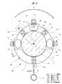
図5に示すように、ボート30は、円盤状に形成された上板30aと、円環状に形成された下板30bと、上板30aと下板30bとの間に設けられ、両者を水平状態で支持する支柱としての第1ボート柱31a,第2ボート柱31bおよび第3ボート柱31cとを備えている。上板30a,下板30bおよび各ボート柱31a〜31cは、何れもSiC等の耐熱材料により形成され、これらは互いに嵌め込みやネジ止め等の接続手段により一体に組み付けられている。<Laminated wafer structure>
As shown in FIG. 5, the
各ボート柱31a〜31cは、何れも同じ形状に形成され、ボート30を組み立てた状態のもとで、各ボート柱31a〜31cが対向する側には、切り欠きよりなる複数のホルダ保持部HSが設けられている。各ホルダ保持部HSは、ウェーハ14を搭載したウェーハホルダ100(図6参照)の外周側を取り外し可能に保持するもので、各ボート柱31a〜31cの長手方向に沿って所定間隔で、例えば30段設けられている。つまり、ボート30は、30枚のウェーハ14を、それぞれウェーハホルダ100を介して水平状態でかつ互いに中心を揃えた状態のもとで、縦方向に積層保持するよう構成されている。 The
第1ボート柱31aおよび第2ボート柱31bは、上板30aおよび下板30bの周方向に沿って90度間隔となるよう配置されている。また、第2ボート柱31bおよび第3ボート柱31cは、上板30aおよび下板30bの周方向に沿って180度間隔となるよう配置されている。つまり、第1ボート柱31aと第2ボート柱31bとの間隔は、第2ボート柱31bと第3ボート柱31cとの間隔よりも狭くなっている。なお、第1ボート柱31aおよび第3ボート柱31cは、第1ボート柱31aおよび第2ボート柱31bの関係と同様に、上板30aおよび下板30bの周方向に沿って90度間隔となっている。各ボート柱31a〜31cの間隔のうちの最も広く開口した開口部分、つまり第2ボート柱31bと第3ボート柱31cとの間の開口部分は、ウェーハ14を保持したウェーハホルダ100を移載するための開口部(搬入搬出部)となっている。 The
ウェーハ14を搭載するウェーハホルダ100は、図6〜図8に示すように円盤状に形成され、当該ウェーハホルダ100は、円環状のホルダベース110と円盤状のホルダカバー120とを備えている。ここで、ホルダベース110およびホルダカバー120においても、何れもSiC等の耐熱材料によりそれぞれ形成されている。なお、ホルダベース110は本発明におけるウェーハホルダを、ホルダカバー120は本発明における蓋部材をそれぞれ構成している。このように、ホルダカバー120によりウェーハ14の上面14bを覆う構成とすることにより、ウェーハ14の上方側から落下してくるパーティクル(微細ゴミ)からウェーハ14を保護することができる。 The
ウェーハホルダ100を構成するホルダベース110の外径寸法は、ウェーハ14の外形寸法よりも大きい外径寸法に設定されている。ホルダベース110の中央部分には、ホルダベース110を軸方向に貫通する貫通穴110aが設けられ、当該貫通穴110aの内周縁には環状段差部111が形成されている。この環状段差部111は、ウェーハ14を保持するようになっている。 The outer diameter of the
このように、ホルダベース110の環状段差部111にウェーハ14を保持させることで、ホルダベース110の中央部分にウェーハ14を精度良く位置決め(搭載)することができ、さらには図6に示すように、各ボート柱31a〜31cとウェーハ14とを遠ざけることができる。また、ウェーハ14を環状段差部111に保持させることで、ウェーハ14の成膜面となる下面14aを反応室44内の雰囲気に曝すことができる。 As described above, by holding the
ホルダベース110は、本体部112と薄肉部113とを備えており、薄肉部113は、ホルダベース110の他の部分、つまり本体部112よりも薄肉に形成されている。これらの本体部112および薄肉部113は、それぞれホルダベース110の径方向に沿って対向配置されている。ウェーハホルダ100をボート30に移載した状態のもとで、本体部112の各ボート柱31a〜31cに対応する部分には、本体部112の厚み方向、つまりウェーハホルダ100の軸方向に沿うよう貫通した第1連通穴112a,第2連通穴112b,第3連通穴112cがそれぞれ設けられている。 The
各連通穴112a〜112cは、何れも同じ形状に形成され、ホルダベース110の周方向に沿う長穴形状に形成されている。各連通穴112a〜112cのホルダベース110の周方向に沿う長さ寸法は、各ボート柱31a〜31cの幅寸法よりも大きく設定され、一方、各連通穴112a〜112cのホルダベース110の径方向に沿う長さ寸法(幅寸法)は、少なくともホルダベース110の最低限の強度を確保し得る大きい寸法に設定されている。つまり、本体部112の径方向に沿う各ボート柱31a〜31cに対応する部分の幅寸法は、少なくともホルダベース110の最低限の強度を確保し得る小さい寸法(幅狭)に設定されている。 Each of the communication holes 112 a to 112 c is formed in the same shape, and is formed in a long hole shape along the circumferential direction of the
本体部112の周方向に沿う第1連通穴112a(第1ボート柱31a)と第2連通穴112b(第2ボート柱31b)との間、および第1連通穴112a(第1ボート柱31a)と第3連通穴112c(第3ボート柱31c)との間には、本体部112の径方向に沿う幅寸法を小さくする一対の切り欠き部112dが形成されている。各切り欠き部112dはそれぞれ同じ形状に形成されている。各切り欠き部112dの本体部112の周方向に沿う長さ寸法は、その両端側が各連通穴112a〜112cに臨む位置にまで延びる長さ寸法に設定されている。ここで、各連通穴112a〜112cおよび各切り欠き部112dは、いずれも各ボート柱31a〜31cによる反応ガスの消費を考慮して設けられるものであり、これらの機能については後述する。 Between the
薄肉部113は、第2ボート柱31bと第3ボート柱31cとの間に配置され、ホルダベース110におけるウェーハ14の下面14a側とは反対側の上面14b側を、例えば切削する(切削加工)ことにより形成されている。薄肉部113は、本体部112のように連通穴や切り欠き部を備えていない。また、薄肉部113の厚み寸法は、本体部112の厚み寸法の略半分の厚み寸法に設定されている。本実施の形態においては、例えば本体部112の厚み寸法を4mmに設定し、薄肉部113の厚み寸法を2mmに設定している。なお、ウェーハ14の厚み寸法は、例えば1mmに設定されている。 The
ここで、薄肉部113を設けることで、ホルダベース110の中心を挟む本体部112側と薄肉部113側とで、当該ホルダベース110の重量バランスを良くしている。つまり、本体部112に設けた各連通穴112a〜112cおよび各切り欠き部112dを設けたことによる本体部112の軽量化に対応し、その反対側を薄肉部113として両者を略同じ重量としている。これにより、ウェーハ14を搭載したウェーハホルダ100が、搬送中に傾斜したりボート30上でがたついたりするのを防止する。 Here, by providing the
ホルダカバー120は、大径本体部121と小径嵌合部122とを備えており、小径嵌合部122は、ホルダベース110の環状段差部111に入り込んで装着されるようになっている。これにより、ホルダベース110に対するホルダカバー120のがたつきを抑制している。小径嵌合部122は、環状段差部111との間でウェーハ14を挟み、ウェーハ14の成膜面である下面14aとは反対側の上面(非成膜面)14bと接触している。このように、ホルダカバー120を、上面14bと接触するよう構成することで、反応ガス(成膜ガス)が上面14bに入り込まず、上面14bが成膜されないようにできる。 The
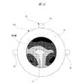
図8はウェーハホルダ100のホルダカバー120を省略し、上方側から見た図であり、ウェーハ14にはハッチングを施している。ウェーハ14を搭載したウェーハホルダ100は、回転機構104(図2,3参照)の回転駆動に伴うボート30の回転により、反応室44内で破線矢印R方向に回転するようになっている。図8においては、ウェーハホルダ100を形成するホルダベース110による反応ガスの消費を説明するために、ウェーハホルダ100の径方向外側から当該ウェーハホルダ100の中心Oまで延びる第1仮想長方形VR1,第2仮想長方形VR2および第3仮想長方形VR3(図中二点鎖線)を記載している。ここで、各仮想長方形VR1〜VR3の短手方向に沿う幅寸法は、各ボート柱31a〜31cの幅寸法(直径寸法)となっている。 FIG. 8 is a view seen from above with the
第1仮想長方形VR1は、第1ボート柱31aに対応する部分に設けられ、当該第1仮想長方形VR1の部分におけるウェーハホルダ100(ホルダベース110)の表面積は、合計でS1(図中網掛部分)に設定されている。このホルダベース110(本体部112)における表面積S1は、第1連通穴112aの大きさに依存し、小さい値に設定されている。 The first virtual rectangle VR1 is provided in a portion corresponding to the
ここで、図8においては、第1ボート柱31aに対応する部分にのみ第1仮想長方形VR1を記載しているが、第2ボート柱31bおよび第3ボート柱31cに対応する部分にも第1仮想長方形VR1と同じ仮想長方形を記載できる。つまり、第2ボート柱31bおよび第3ボート柱31cに対応する部分の仮想長方形(図示せず)におけるホルダベース110の表面積についても、上述と同様に合計でS1に設定されている。 Here, in FIG. 8, the first virtual rectangle VR1 is shown only in the portion corresponding to the
第2仮想長方形VR2は、ウェーハホルダ100の中心Oを中心として、第1仮想長方形VR1を図中左側へ45度傾けた位置、つまり第1ボート柱31aと第2ボート柱31bとの間の中間位置まで回転させた位置に設けられている。第2仮想長方形VR2の部分におけるホルダベース110の表面積は、第1仮想長方形VR1の部分の表面積S1よりも大きい表面積S2(図中網掛部分)に設定、つまり第1仮想長方形VR1の部分の表面積S1は、第2仮想長方形VR2の部分の表面積S2よりも小さくなっている(S1<S2)。第2仮想長方形VR2の部分における本体部112には、切り欠き部112dを設けているが、当該切り欠き部112dのウェーハホルダ100の径方向に沿う幅寸法よりも、第1仮想長方形VR1の部分に対応して設けた第1連通穴112aのウェーハホルダ100の径方向に沿う幅寸法の方が大きいため、表面積S2>表面積S1となる。 The second virtual rectangle VR2 is centered on the center O of the
ここで、図8においては、第1ボート柱31aと第2ボート柱31bとの間にのみ第2仮想長方形VR2を記載しているが、第1ボート柱31aと第3ボート柱31cとの間にも第2仮想長方形VR2と同じ仮想長方形を記載できる。つまり、第1ボート柱31aと第3ボート柱31cとの間の中間位置における仮想長方形(図示せず)においても、そのホルダベース110の表面積は上述と同様にS2に設定される。 Here, in FIG. 8, the second virtual rectangle VR2 is shown only between the
第3仮想長方形VR3は、ウェーハホルダ100の中心Oを中心として、第1仮想長方形VR1を図中左右側のいずれか一方に180度傾けた位置、つまり第2ボート柱31bと第3ボート柱31cとの間で、中心Oを挟む第1ボート柱31aの反対側にある薄肉部113の中間位置まで回転させた位置に設けられている。第3仮想長方形VR3の部分におけるホルダベース110の表面積は、第2仮想長方形VR2の部分の表面積S2よりも大きい表面積S3(図中網掛部分)に設定、つまり第2仮想長方形VR2の部分の表面積S2は、切り欠き部112dを設けた分、第3仮想長方形VR3の部分の表面積S3よりも小さくなっている(S2<S3)。 The third virtual rectangle VR3 is a position where the first virtual rectangle VR1 is tilted 180 degrees to either the left or right side in the figure with respect to the center O of the
このように、各ボート柱31a〜31cに対応する部分のホルダベース110の表面積をS1とし、第1ボート柱31aと第2ボート柱31bとの間および第1ボート柱31aと第3ボート柱31cとの間のホルダベース110の表面積をS2とし、第2ボート柱31bと第3ボート柱31cとの間のホルダベース110の表面積をS3とし、これらの大小関係をS1<S2<S3としている。これにより、図中矢印に示すように、第1ガス供給ノズル61の各第1ガス供給口60から供給される反応ガスは、各ボート柱31a〜31cに対応する部分では、各ボート柱31a〜31cおよび表面積S1の部分(消費位置A)で消費される。また、第1ボート柱31aと第2ボート柱31bとの間および第1ボート柱31aと第3ボート柱31cとの間では、反応ガスは表面積S2の部分(消費位置B)で消費される。さらに、第2ボート柱31bと第3ボート柱31cとの間では、反応ガスは表面積S3の部分(消費位置C)で消費される。 As described above, the surface area of the
ここで、各消費位置A〜Cにおける反応ガスの消費量は、何れの部分においても略同じ消費量となるようバランスされている。例えば、消費位置Cではホルダベース110の表面積S3の部分で消費量20%となり、消費位置Aでは各ボート柱31a〜31cで消費量18%、ホルダベース110の表面積S1の部分で消費量2%となる。消費位置Bでは、消費位置Cに比して各ボート柱31a〜31cに近接しており、これにより各ボート柱31a〜31cでの消費(消費量5%)が影響する。このため、消費位置Bでは、切り欠き部112dを設けて反応ガスの消費量を微調整(消費量15%となるよう調整)している。 Here, the consumption amount of the reactive gas at each of the consumption positions A to C is balanced so as to be substantially the same consumption amount in any part. For example, at the consumption position C, the consumption is 20% at the surface area S3 of the
このように各消費位置A〜Cにおいて反応ガスの消費量をバランス、つまり各消費位置A〜Cの全て部分において、上述の例示のようにウェーハ14に到達するまでの反応ガスの消費量を略20%とすることができ、ひいてはウェーハ14に到達するまでの反応ガスの濃度を略均一化できるようにしている。即ち、本実施の形態における各連通穴112a〜112cの大きさや、切り欠き部112dの大きさは、上述したような反応ガスの消費量を考慮に入れて設定されると良い。 In this way, the amount of reaction gas consumed at each of the consumption positions A to C is balanced, that is, the amount of reaction gas consumed until reaching the
<SiCエピタキシャル膜の成膜方法>
次に、上述した半導体製造装置10を用い、半導体デバイスの製造工程の一工程として、SiC等で構成されるウェーハ14等の基板上に、例えば、SiCエピタキシャル膜を成膜する基板の製造方法(処理方法)について説明する。なお、以下の説明における半導体製造装置10を構成する各部分の動作は、コントローラ152によって制御される。<Method for Forming SiC Epitaxial Film>
Next, using the
図1に示すように、まず、ポッドステージ18に、複数枚のウェーハ14(ウェーハホルダ100)を収納したポッド16をセットする。すると、ポッド搬送装置20が動作して、ポッド16がポッドステージ18からポッド収納棚22へ搬送されてストックされる。次に、ポッド搬送装置20により、ポッド収納棚22にストックされたポッド16をポッドオープナ24に搬送してセットし、当該ポッドオープナ24によりポッド16の蓋16aが開かれて、基板枚数検知器26によりポッド16に収納されているウェーハ14の枚数を検知する。 As shown in FIG. 1, first, a
その後、基板移載機28の動作により、ポッドオープナ24の位置にあるポッド16からウェーハ14を搭載したウェーハホルダ100を取り出し、ボート30に移載する。 Thereafter, the
複数枚のウェーハ14をボート30に積層すると、各ウェーハ14を保持したボート30は、昇降モータMの回転駆動による昇降台114および昇降シャフト124の昇降動作により反応室44内に搬入、つまりボートローディングされる。ボート30が反応室44内に完全に搬入されると、シールキャップ102は反応室44をシールした状態となり、これにより反応室44の気密が保持される。ここまでの一連の工程、つまりボート30に複数積層された各ウェーハ14を反応管42内に搬入し、シールキャップ102により密閉するまでの工程(ボートローディング工程)が、基板搬送工程を構成している。 When a plurality of
ボート30を反応室44に搬入した後、反応室44の内部圧力が所定の圧力(真空度)となるよう真空排気装置80が駆動され、反応室44が真空排気(真空引き)される。この時、反応室44の内部圧力は、圧力センサによって測定され、測定された圧力に基づいて第1ガス排気口62および第2ガス排気口66に連通するAPCバルブ79がフィードバック制御される。 After carrying the
また、ウェーハ14の温度および反応室44の内部温度を所定の温度とするよう、誘導コイル50が通電され、これにより加熱体48が加熱される。この時、反応室44の内部温度が所定の温度分布(例えば均一温度分布)となるよう、温度センサが検出した温度情報に基づいて誘導コイル50への通電具合をフィードバック制御する。続いて、回転機構104によりボート30が回転駆動されて、これにより各ウェーハ14も反応室44の内部で回転される(図8の破線矢印R参照)。 Further, the
その後、MFC72a〜72dおよびバルブ74a〜74dを制御し、これにより、SiCエピタキシャル膜の成膜に寄与するSi原子含有ガス(成膜ガス),Cl原子含有ガス(エッチングガス),C原子含有ガス(成膜ガス)およびH2ガス(還元ガス)を、各ガス源70a〜70dから供給する。すると、これらのガスは第1ガスライン68内で混合されて、その後、反応ガスとして第1ガスライン68を介して第1ガス供給ノズル61の各第1ガス供給口60から、反応室44内の各ウェーハ14および各ウェーハホルダ100に向けて反応ガスが噴射される。Thereafter, the
各第1ガス供給口60から噴射された反応ガスは、反応室44内を横切る際に、各ボート柱31a〜31c,各ウェーハ14および各ウェーハホルダ100に接触する。これにより、各ウェーハ14における下面14a(図6参照)の表面上等に、SiCエピタキシャル膜が成膜されていく。その後、反応室44内の加熱体48の内周側等を流れて、第1ガス排気口62からガス排気管76を介して外部に排気される。 The reaction gas injected from each first
また、MFC72eおよびバルブ74eが制御され、第5ガス源70eからの不活性ガスとしてのArガス(希ガス)が所定の流量となるよう調整される。そして、第2ガスライン69,第2ガス供給ノズル65および第2ガス供給口64を介して反応管42と断熱材54との間に供給される。第2ガス供給口64から供給されたArガスは、反応管42と断熱材54との間を流れて、第2ガス排気口66から外部に排気される。その後、上述のように反応ガスを各ウェーハ14等に曝して、予め設定された時間が経過すると、各反応ガスの供給制御が停止される。ここまでの一連の工程、つまり反応ガスの供給により、各ウェーハ14における下面14aの表面上等にSiCエピタキシャル膜を成膜する工程が、基板処理工程を構成している。 Further, the
次いで、図示しない不活性ガス供給源から不活性ガスが供給され、反応室44内の加熱体48の内側の空間が不活性ガスで置換され、さらに反応室44の内部圧力が常圧に復帰される。 Next, an inert gas is supplied from an inert gas supply source (not shown), the space inside the
反応室44内が常圧に復帰した後、昇降モータMの回転駆動によりシールキャップ102が下降し、処理炉40の炉口144が開口される。これに伴い、熱処理済み(成膜処理済み)の各ウェーハ14が、ボート30に保持された状態でマニホールド36の下方側から反応管42の外部に搬出、つまりボートアンローディングされる。ボート30に保持された各ウェーハ14は、冷えるまでロードロック室LRの内部で待機状態となる。 After the inside of the
その後、各ウェーハ14が所定の温度にまで冷却されると、基板移載機28の動作により、各ウェーハ14を搭載した各ウェーハホルダ100がボート30から取り出され、ポッドオープナ24にセットされている空のポッド16に搬送されて収納される。その後、ポッド搬送装置20の動作により、各ウェーハ14を収納したポッド16が、ポッド収納棚22またはポッドステージ18に搬送される。このようにして、半導体製造装置10の一連の動作が完了する。 Thereafter, when each
<成膜状態の比較>
次に、ウェーハホルダ100を用いた場合のSiCエピタキシャル膜の成膜状態(本発明)と、図9に示す単純な円環形状のウェーハホルダWHを用いた場合のSiCエピタキシャル膜の成膜状態(比較例)との比較結果について、図面を用いて詳細に説明する。<Comparison of film formation state>
Next, the film formation state of the SiC epitaxial film when the
図9は単純な円環形状のウェーハホルダ(比較例)を示す図7に対応した斜視図を、図10は図9の比較例に係るウェーハホルダを用いたウェーハの成膜状態を示す解析図を、図11は本発明に係るウェーハホルダを用いたウェーハの成膜状態を示す解析図をそれぞれ表している。 9 is a perspective view corresponding to FIG. 7 showing a simple ring-shaped wafer holder (comparative example), and FIG. 10 is an analysis diagram showing a film formation state of a wafer using the wafer holder according to the comparative example of FIG. FIG. 11 is an analysis diagram showing a film formation state of a wafer using the wafer holder according to the present invention.
図9に示すように、比較例に係るウェーハホルダWHは、上述の第1実施の形態に比してホルダベースHBの形状のみが異なっている。ホルダベースHBは、その肉厚が全周で均一となって凹凸の無い単純な円環形状に形成され、各ボート柱31a〜31cに対応する連通穴や、各ボート柱31a〜31c間に対応する切り欠き部を備えていない。つまり、比較例のウェーハホルダWHは、各ボート柱31a〜31cからウェーハ14を離間させるのみで、ある程度の成膜精度を確保するようにしている。なお、図9において、ホルダベースHBの形状以外については、上述の第1実施の形態と同じ構成であるため同一の記号を付している。 As shown in FIG. 9, the wafer holder WH according to the comparative example differs from the first embodiment described above only in the shape of the holder base HB. The holder base HB is formed in a simple annular shape having a uniform thickness over the entire circumference and without irregularities, and corresponds to the communication holes corresponding to the
図10に示すように、ホルダベースHBによれば、ウェーハ14における第2ボート柱31bと第3ボート柱31cとの間、つまり各ボート柱31b,31cによる悪影響を受け難い部分については、意図する膜厚のSiCエピタキシャル膜が部分的に成膜されている(図中濃色部分)。ところが、ウェーハ14のそれ以外の部分については、各ボート柱31a〜31cやホルダベースHBが反応ガスを消費することから、SiCエピタキシャル膜が薄くなっている(図中淡色部分)。さらに、図中濃色部分と図中淡色部分との境界線の間隔は詰まっており急勾配となっている。これは、ウェーハ14における成膜面の凹凸の差が大きいことを意味し、後の半導体デバイス等における製品誤差を招く原因となる。 As shown in FIG. 10, according to the holder base HB, a portion between the
これに対し、第1実施の形態におけるホルダベース110によれば、各ボート柱31b,31cによる悪影響を受け難い部分以外の部分における反応ガスの消費量を調整(コントロール)しているので、図11に示すように、ウェーハ14における成膜面の大部分を、意図する膜厚にすることができる(図中濃色部分を増やすことができる)。また、比較例とは異なり、図中濃色部分と図中淡色部分との境界線の間隔が広がり、緩勾配となっている。これは、ウェーハ14における成膜面の凹凸の差が小さいことを意味し、後の半導体デバイス等における製品誤差を小さくすることができる。 On the other hand, according to the
<第1実施の形態の代表的効果>
以上、第1実施の形態で説明した技術的思想によれば、少なくとも、以下に記載する複数の効果のうち、1つ以上の効果を奏する。<Typical effects of the first embodiment>
As described above, according to the technical idea described in the first embodiment, at least one of the plurality of effects described below is produced.
(1)第1実施の形態によれば、ウェーハ14を内周側で保持するウェーハホルダ100(ホルダベース110)と、ホルダベース110の外周側を保持するホルダ保持部HSを有する各ボート柱31a〜31cとを備え、ホルダベース110の外径寸法をウェーハ14の外径寸法よりも大きくし、かつホルダベース110をホルダ保持部HSから取り外せるようにしたので、ホルダベース110と各ボート柱31a〜31cとを溶接等により固着しなくて済む。したがって、ホルダベース110および各ボート柱31a〜31cをSiC等で形成することができ、容易に高温に耐え得るウェーハの積層構造を実現できる。また、ホルダベース110によって、各ボート柱31a〜31cからウェーハ14を離間させることができるので、成膜精度に悪影響を及ぼすのを抑制できる。 (1) According to the first embodiment, each
(2)第1実施の形態によれば、第1ボート柱31aの幅寸法で、ホルダベース110の中心Oまで延ばした第1仮想長方形VR1におけるホルダベース110の表面積S1を、第1仮想長方形VR1をホルダベース110の中心Oを中心として、各ボート柱31a〜31cのうちの第1,第2ボート柱31a,31bの中間位置まで回転させた第2仮想長方形VR2におけるホルダベース110の表面積S2よりも小さくした。これにより、ホルダベース110を、第1ボート柱31aによる反応ガスの消費を考慮した形状とすることができ、ウェーハ14に到達する反応ガスの濃度をその全周において略均一化できる。よって、成膜精度をより向上させることが可能となる。 (2) According to the first embodiment, the surface area S1 of the
(3)第1実施の形態によれば、第1,第2ボート柱31a,31bの間隔を第2,第3ボート柱31b,31cの間隔よりも狭くし、第2仮想長方形VR2は第1,第2ボート柱31a,31bの中間位置に位置し、第2仮想長方形VR2におけるホルダベース110の表面積S2を、第1仮想長方形VR1をホルダベース110の中心Oを中心として、第2,第3ボート柱31b,31cの中間位置まで回転させた第3仮想長方形VR3におけるホルダベース110の表面積S3よりも小さくした。これにより、間隔が狭い側の第1,第2ボート柱31a,31bによる反応ガスの消費を考慮することができる。よって、ウェーハ14に到達する反応ガスの濃度をその全周においてさらに均一化することができ、成膜精度をさらに向上させることが可能となる。 (3) According to the first embodiment, the interval between the first and
(4)第1実施の形態で説明した半導体製造装置10を、半導体装置の製造方法における基板の処理工程において用いることにより、半導体装置の製造方法において、上述した複数の効果のうち、1つ以上の効果を奏する。 (4) By using the
(5)第1実施の形態で説明した半導体製造装置10を、SiCエピタキシャル膜を形成する基板の製造方法における基板の処理工程において用いることにより、SiCエピタキシャル膜を形成する基板の製造方法において、上述した複数の効果のうち、1つ以上の効果を奏する。 (5) In the substrate manufacturing method for forming a SiC epitaxial film, the
[第2実施の形態]
次に、本発明の第2実施の形態について、図面を参照しつつ詳細に説明する。なお、上述した第1実施の形態と同じ部分については同一の記号を付し、その詳細な説明を省略する。[Second Embodiment]
Next, a second embodiment of the present invention will be described in detail with reference to the drawings. The same parts as those in the first embodiment described above are denoted by the same reference numerals, and detailed description thereof is omitted.
図12は第2実施の形態に係るウェーハホルダを示す図7に対応した斜視図を、図13は図12のウェーハホルダにおける反応ガスの消費部分を説明する説明図をそれぞれ表している。 FIG. 12 is a perspective view corresponding to FIG. 7 showing the wafer holder according to the second embodiment, and FIG. 13 is an explanatory diagram for explaining the consumption part of the reactive gas in the wafer holder of FIG.
第2実施の形態においては、上述の第1実施の形態に比してウェーハホルダ200を形成するホルダベース210の形状のみが異なっている。つまり、第1実施の形態ではホルダベース110に一対の切り欠き部112d(図7参照)を設け、その外周側を非円形としたのに対し、第2実施の形態ではホルダベース210に各切り欠き部112dを設けず、その外周側を円形としている。ホルダベース210は、各切り欠き部112dに換えて一対の抜き穴211を備えており、各抜き穴211は各切り欠き部112dと同じ機能を有している。各抜き穴211は、第1ボート柱31aと第2ボート柱31bとの間、および第1ボート柱31aと第3ボート柱31cとの間にそれぞれ設けられ、ウェーハホルダ200の軸方向に沿うようホルダベース210の本体部212を貫通して設けられている。 In the second embodiment, only the shape of the
各抜き穴211(第2実施の形態)は、各切り欠き部112d(第1実施の形態)に比して径方向内側に配置されるため、ホルダベース210の第2仮想長方形VR2の部分の表面積S20(図13参照)と、図8に示す表面積S2とを略同じ表面積とするために、各抜き穴211の径方向に沿う幅寸法を、各切り欠き部112dの径方向に沿う幅寸法よりも大きくしている。これにより、ホルダベース210の本体部212側の重量は、図8に示すホルダベース110の本体部112側の重量よりも軽くなっている。したがって、ホルダベース210の中心Oを挟む本体部212側の重量と薄肉部213側の重量とをバランスさせるために、薄肉部213には円弧穴213aを設けている。円弧穴213aは、ウェーハホルダ200の軸方向に沿うようホルダベース210の薄肉部213を貫通して設けられている。 Since each punched hole 211 (second embodiment) is disposed radially inward of each
ここで、ホルダベース210の第3仮想長方形VR3の部分の表面積S30は、図8に示す表面積S3よりも若干小さくなっているため、これに合わせて、第1,第2仮想長方形VR1,VR2の部分の表面積S10,S20も、図8に示す表面積S1,S2よりも若干小さく設定されている。これにより、第1実施の形態と同様、各ウェーハ14に到達する反応ガスの濃度をその全周において略均一化させている。なお、第2実施の形態のウェーハホルダ200によるウェーハ14の膜厚状態は、図11に示すように、第1実施の形態と略同じ結果となる。 Here, the surface area S30 of the third virtual rectangle VR3 of the
<第2実施の形態の代表的効果>
以上、第2実施の形態で説明した技術的思想においても、上述した第1実施の形態と同様の作用効果を奏することができる。これに加え、第2実施の形態においては、第1ボート柱31aと第2ボート柱31bとの間および第1ボート柱31aと第3ボート柱31cとの間に、ウェーハホルダ200(ホルダベース210)の軸方向に沿う各抜き穴211を設けたので、ホルダベース210の外周側を円形にできる。したがって、第1ガス供給ノズル61の第1ガス供給口60から供給される反応ガスの流れ方向が乱れるのを抑制して、各ウェーハ14への反応ガスの供給をより安定化させることができる。<Typical effects of the second embodiment>
As mentioned above, also in the technical idea demonstrated in 2nd Embodiment, there can exist an effect similar to 1st Embodiment mentioned above. In addition, in the second embodiment, the wafer holder 200 (holder base 210) is provided between the
以上、本発明者によってなされた発明を実施の形態に基づき具体的に説明したが、本発明は上述した各実施の形態に限定されるものではなく、その要旨を逸脱しない範囲で種々変更可能であることは言うまでもない。例えば、上記各実施の形態においては、SiCエピタキシャル膜を成膜する成膜装置(基板処理装置)を例示して説明したが、本発明はこれに限らず、他の形式の基板処理装置にも本発明における技術的思想を適用することができる。 As mentioned above, the invention made by the present inventor has been specifically described based on the embodiments. However, the present invention is not limited to the above-described embodiments, and various modifications can be made without departing from the scope of the invention. Needless to say. For example, in each of the embodiments described above, the film forming apparatus (substrate processing apparatus) for forming the SiC epitaxial film has been described as an example. However, the present invention is not limited to this, and other types of substrate processing apparatuses may be used. The technical idea of the present invention can be applied.
本発明は少なくとも以下の実施の形態を含む。 The present invention includes at least the following embodiments.
〔付記1〕
複数積層された基板を処理する反応容器と、
前記反応容器内に設けられ、前記基板に反応ガスを供給するガスノズルと、
前記基板を内周側で保持する複数のウェーハホルダと、
前記ウェーハホルダの外周側を保持するホルダ保持部を有する複数のボート柱とを備え、
前記ウェーハホルダの外径寸法を前記基板の外径寸法よりも大きくし、かつ前記ウェーハホルダを前記ホルダ保持部から取り外せるようにしたことを特徴とする基板処理装置。[Appendix 1]
A reaction vessel for processing a plurality of stacked substrates;
A gas nozzle provided in the reaction vessel for supplying a reaction gas to the substrate;
A plurality of wafer holders for holding the substrate on the inner peripheral side;
A plurality of boat pillars having a holder holding portion for holding the outer peripheral side of the wafer holder;
A substrate processing apparatus, wherein an outer diameter of the wafer holder is larger than an outer diameter of the substrate, and the wafer holder can be removed from the holder holding portion.
〔付記2〕
前記ボート柱の幅寸法で、前記ウェーハホルダの中心まで延ばした第1仮想長方形における前記ウェーハホルダの表面積を、前記第1仮想長方形を前記ウェーハホルダの中心を中心として、前記複数のボート柱のうちの2つの前記ボート柱の中間位置まで回転させた第2仮想長方形における前記ウェーハホルダの表面積よりも小さくしたことを特徴とする付記1記載の基板処理装置。[Appendix 2]
The surface area of the wafer holder in a first virtual rectangle extending to the center of the wafer holder with the width dimension of the boat column, the first virtual rectangle being centered on the center of the wafer holder, 2. The substrate processing apparatus according to
〔付記3〕
前記複数のボート柱を第1,第2,第3ボート柱から形成し、前記第1,第2ボート柱の間隔を前記第2,第3ボート柱の間隔よりも狭くし、前記第2仮想長方形は前記第1,第2ボート柱の中間位置に位置し、前記第2仮想長方形における前記ウェーハホルダの表面積を、前記第1仮想長方形を前記ウェーハホルダの中心を中心として、前記第2,第3ボート柱の中間位置まで回転させた第3仮想長方形における前記ウェーハホルダの表面積よりも小さくしたことを特徴とする付記2記載の基板処理装置。[Appendix 3]
The plurality of boat pillars are formed from first, second, and third boat pillars, and an interval between the first and second boat pillars is made smaller than an interval between the second and third boat pillars, and the second virtual pillar A rectangle is located at an intermediate position between the first and second boat pillars, and the surface area of the wafer holder in the second virtual rectangle is defined by the second virtual rectangle with the first virtual rectangle as the center of the wafer holder. 3. The substrate processing apparatus according to
〔付記4〕
前記ウェーハホルダの外周側で前記第1ボート柱と前記第2ボート柱との間に、前記ウェーハホルダの径方向に沿う切り欠き部を設けたことを特徴とする付記3記載の基板処理装置。[Appendix 4]
4. The substrate processing apparatus according to appendix 3, wherein a notch portion is provided along the radial direction of the wafer holder between the first boat column and the second boat column on the outer peripheral side of the wafer holder.
〔付記5〕
前記ウェーハホルダの外周側を円形とし、前記第1ボート柱と前記第2ボート柱との間に、前記ウェーハホルダの軸方向に沿う抜き穴を設けたことを特徴とする付記3記載の基板処理装置。[Appendix 5]
4. The substrate processing according to claim 3, wherein an outer peripheral side of the wafer holder is circular, and a punched hole is provided between the first boat column and the second boat column along the axial direction of the wafer holder. apparatus.
〔付記6〕
前記ウェーハホルダの前記第2ボート柱と前記第3ボート柱との間の厚み寸法を、前記ウェーハホルダの他の部分の厚み寸法よりも薄くしたことを特徴とする付記2記載の基板処理装置。[Appendix 6]
3. The substrate processing apparatus according to
〔付記7〕
前記ウェーハホルダの厚みを薄くした薄肉部を、前記ウェーハホルダの前記基板の成膜面側とは反対側を切削することで形成したことを特徴とする付記6記載の基板処理装置。[Appendix 7]
The substrate processing apparatus according to appendix 6, wherein the thinned portion having a reduced thickness of the wafer holder is formed by cutting a side of the wafer holder opposite to the film forming surface side of the substrate.
〔付記8〕
前記ウェーハホルダの内周側に、前記ウェーハホルダの軸方向に貫通する貫通穴を設け、前記ウェーハホルダに装着され、前記基板の成膜面側とは反対側を覆う蓋部材を設けたことを特徴とする付記1ないし7のいずれか1つに記載の基板処理装置。[Appendix 8]
A through-hole penetrating in the axial direction of the wafer holder is provided on the inner peripheral side of the wafer holder, and a lid member that is attached to the wafer holder and covers a side opposite to the film formation surface side of the substrate is provided. 8. The substrate processing apparatus according to any one of
〔付記9〕
前記ウェーハホルダの前記第1仮想長方形に対応する部分には、前記ウェーハホルダの軸方向に沿う連通穴を設けたことを特徴とする付記8記載の基板処理装置。[Appendix 9]
9. The substrate processing apparatus according to
本発明は、半導体装置(半導体デバイス)やSiCエピタキシャル膜を形成する基板などを製造する製造業等に幅広く利用することができる。 The present invention can be widely used in manufacturing industries that manufacture semiconductor devices (semiconductor devices), substrates on which SiC epitaxial films are formed, and the like.
10…半導体製造装置(基板処理装置)、12…筐体、14…ウェーハ(基板)、14a…下面、14b…上面、16…ポッド、16a…蓋、18…ポッドステージ、20…ポッド搬送装置、22…ポッド収納棚、24…ポッドオープナ、26…基板枚数検知器、28…基板移載機、30…ボート、30a…上板、30b…下板、31a…第1ボート柱、31b…第2ボート柱、31c…第3ボート柱、32…アーム、34…ボート断熱部、36…マニホールド、40…処理炉、42…反応管、44…反応室、48…加熱体、50…誘導コイル、51…支持部材、52…温度制御部、54…断熱材、54a…側壁部、54b…蓋部、55…外側断熱壁、58…磁気シール、60…第1ガス供給口、61…第1ガス供給ノズル、62…第1ガス排気口、64…第2ガス供給口、65…第2ガス供給ノズル、66…第2ガス排気口、68…第1ガスライン、69…第2ガスライン、70a…第1ガス源、70b…第2ガス源、70c…第3ガス源、70d…第4ガス源、70e…第5ガス源、72a〜72e…MFC、74a〜74e…バルブ、76…ガス排気管、78…ガス流量制御部、79…APCバルブ、80…真空排気装置、98…圧力制御部、100…ウェーハホルダ、102…シールキャップ、104…回転機構、106…回転軸、108…駆動制御部、110…ホルダベース(ウェーハホルダ)、110a…貫通穴、111…環状段差部、112…本体部、112a…第1連通穴、112b…第2連通穴、112c…第3連通穴、112d…切り欠き部、113…薄肉部、114…昇降台、116…ガイドシャフト、118…ボール螺子、120…ホルダカバー(蓋部材)、121…大径本体部、122…小径嵌合部、124…昇降シャフト、126…天板、126a…貫通孔、128…ベローズ、130…昇降基板、132…駆動部カバー、134…駆動部収納ケース、135…冷却機構、138…電力ケーブル、140…冷却水流路、142…冷却水配管、144…炉口、150…主制御部、152…コントローラ、200…ウェーハホルダ、210…ホルダベース(ウェーハホルダ)、211…抜き穴、212…本体部、213…薄肉部、213a…円弧穴、M…昇降モータ、LR…ロードロック室、UP…上基板、LP…下基板、WH…ウェーハホルダ、HB…ホルダベース、HS…ホルダ保持部、VR1…第1仮想長方形、VR2…第2仮想長方形、VR3…第3仮想長方形 DESCRIPTION OF
Claims (4)
Translated fromJapanese前記反応容器内に設けられ、前記基板に反応ガスを供給するガスノズルと、
前記基板を内周側で保持し、前記基板の外径寸法よりも大きい外径寸法のウェーハホルダと、
前記ウェーハホルダを取り外せるようにその外周側を保持するホルダ保持部を有する複数のホルダ保持柱とを備え、
前記ウェーハホルダは、
前記ウェーハホルダを前記ホルダ保持部に保持させた状態のもとで、前記ウェーハホルダの前記ホルダ保持部側に設けられる本体部と、前記基板を中心に前記ウェーハホルダの前記ホルダ保持部側とは反対側に設けられ、前記本体部よりも薄肉とされた薄肉部とを有し、
前記ホルダ保持柱の幅寸法で、前記ウェーハホルダの径方向外側から前記基板の中心まで延ばした第1仮想長方形における前記本体部の表面積を、前記本体部に連通穴を設けることで、前記第1仮想長方形を前記基板の中心を中心として、前記薄肉部まで回転させた第3仮想長方形における前記薄肉部の表面積よりも小さくし、
前記第3仮想長方形における前記薄肉部の重量を、薄く加工することで、前記第1仮想長方形における前記本体部の重量と略同じ重量にしたことを特徴とする基板処理装置。A reaction vessel for processing the substrate;
A gas nozzle provided in the reaction vessel for supplying a reaction gas to the substrate;
Holding the substrate on the inner peripheral side, a wafer holder having an outer diameter larger than the outer diameter of the substrate;
A plurality of holder holding pillars having a holder holding portion for holding the outer peripheral side so that the wafer holder can be removed;
The wafer holder is
Under the state where the wafer holder is held by the holder holding part, a main body part provided on the holder holding part side of the wafer holder and the holder holding part side of the wafer holder centering on the substrate A thin portion provided on the opposite side and made thinner than the main body,
A surface area of the main body portion in a first imaginary rectangle extendingfrom the outside in the radial direction of the wafer holder to the center of the substrate with the width dimension of the holder holding column is provided with a communication hole in the main body portion. The virtual rectangle is made smaller than the surface area of the thin portion in the third virtual rectangle rotated around the center of the substrate to the thin portion,
The substrate processing apparatus according to claim 1, wherein a weight of the thin portion in the third virtual rectangle is thinned to be substantially the same as a weight of the main body portion in the first virtual rectangle.
前記ホルダ保持部に保持させた状態のもとで、前記ホルダ保持部側に設けられる本体部と、前記基板を中心に前記ホルダ保持部側とは反対側に設けられ、前記本体部よりも薄肉とされた薄肉部とを有し、
前記ホルダ保持柱の幅寸法で、前記ウェーハホルダの径方向外側から前記基板の中心まで延ばした第1仮想長方形における前記本体部の表面積を、前記本体部に連通穴を設けることで、前記第1仮想長方形を前記基板の中心を中心として、前記薄肉部まで回転させた第3仮想長方形における前記薄肉部の表面積よりも小さくし、
前記第3仮想長方形における前記薄肉部の重量を、薄く加工することで、前記第1仮想長方形における前記本体部の重量と略同じ重量にしたウェーハホルダに、前記基板を移載する工程と、
前記ウェーハホルダに保持された前記基板を反応容器内に搬入する工程と、
前記基板を前記反応容器内で処理する工程と、
前記基板を搬出する工程と、を有することを特徴とする半導体装置の製造方法。Holding the substrate on the inner peripheral side, the outer diameter dimension is larger than the outer diameter dimension of the substrate, the outer peripheral side is held so that it can be removed to a holder holding portion provided in a plurality of holder holding columns,
A main body provided on the holder holding portion side under a state of being held by the holder holding portion, and provided on the opposite side of the holder holding portion side with respect to the substrate, and thinner than the main body portion. A thin-walled portion,
A surface area of the main body portion in a first imaginary rectangle extendingfrom the outside in the radial direction of the wafer holder to the center of the substrate with the width dimension of the holder holding column is provided with a communication hole in the main body portion. The virtual rectangle is made smaller than the surface area of the thin portion in the third virtual rectangle rotated around the center of the substrate to the thin portion,
Transferring the substrate to a wafer holder having a weight substantially equal to the weight of the main body in the first virtual rectangle by thinly processing the weight of the thin portion in the third virtual rectangle;
Carrying the substrate held by the wafer holder into a reaction vessel;
Processing the substrate in the reaction vessel;
And a step of unloading the substrate.
前記ウェーハホルダは、
前記基板を内周側で保持し、前記基板の外径寸法よりも大きい外径寸法とされ、その外周側が、複数のホルダ保持柱に設けられたホルダ保持部に取り外せるように保持され、
前記ウェーハホルダを前記ホルダ保持部に保持させた状態のもとで、前記ウェーハホルダの前記ホルダ保持部側に設けられる本体部と、前記基板を中心に前記ウェーハホルダの前記ホルダ保持部側とは反対側に設けられ、前記本体部よりも薄肉とされた薄肉部とを有し、
前記ホルダ保持柱の幅寸法で、前記ウェーハホルダの径方向外側から前記基板の中心まで延ばした第1仮想長方形における前記本体部の表面積を、前記本体部に連通穴を設けることで、前記第1仮想長方形を前記基板の中心を中心として、前記薄肉部まで回転させた第3仮想長方形における前記薄肉部の表面積よりも小さくし、
前記第3仮想長方形における前記薄肉部の重量を、薄く加工することで、前記第1仮想長方形における前記本体部の重量と略同じ重量にしたことを特徴とするウェーハホルダ。A wafer holder used in a substrate processing apparatus for processing a substrate,
The wafer holder is
The substrate is held on the inner peripheral side, the outer diameter dimension is larger than the outer diameter dimension of the substrate, the outer peripheral side is held so as to be detachable to a holder holding portion provided on a plurality of holder holding columns,
Under the state where the wafer holder is held by the holder holding part, a main body part provided on the holder holding part side of the wafer holder and the holder holding part side of the wafer holder centering on the substrate A thin portion provided on the opposite side and made thinner than the main body,
A surface area of the main body portion in a first imaginary rectangle extendingfrom the outside in the radial direction of the wafer holder to the center of the substrate with the width dimension of the holder holding column is provided with a communication hole in the main body portion. The virtual rectangle is made smaller than the surface area of the thin portion in the third virtual rectangle rotated around the center of the substrate to the thin portion,
The wafer holder according to claim 1, wherein the weight of the thin portion in the third virtual rectangle is made to be substantially the same as the weight of the main body portion in the first virtual rectangle by thinning.
Priority Applications (3)
| Application Number | Priority Date | Filing Date | Title |
|---|---|---|---|
| JP2011041214AJP5881956B2 (en) | 2011-02-28 | 2011-02-28 | Substrate processing apparatus, semiconductor device manufacturing method, and wafer holder |
| US13/405,638US20120220107A1 (en) | 2011-02-28 | 2012-02-27 | Substrate processing apparatus, wafer holder, and method of manufacturing semiconductor device |
| CN201210055696.9ACN102655107B (en) | 2011-02-28 | 2012-02-28 | The manufacture method of lining processor, chip support and semiconductor device |
Applications Claiming Priority (1)
| Application Number | Priority Date | Filing Date | Title |
|---|---|---|---|
| JP2011041214AJP5881956B2 (en) | 2011-02-28 | 2011-02-28 | Substrate processing apparatus, semiconductor device manufacturing method, and wafer holder |
Publications (3)
| Publication Number | Publication Date |
|---|---|
| JP2012178491A JP2012178491A (en) | 2012-09-13 |
| JP2012178491A5 JP2012178491A5 (en) | 2014-04-10 |
| JP5881956B2true JP5881956B2 (en) | 2016-03-09 |
Family
ID=46719270
Family Applications (1)
| Application Number | Title | Priority Date | Filing Date |
|---|---|---|---|
| JP2011041214AActiveJP5881956B2 (en) | 2011-02-28 | 2011-02-28 | Substrate processing apparatus, semiconductor device manufacturing method, and wafer holder |
Country Status (3)
| Country | Link |
|---|---|
| US (1) | US20120220107A1 (en) |
| JP (1) | JP5881956B2 (en) |
| CN (1) | CN102655107B (en) |
Families Citing this family (21)
| Publication number | Priority date | Publication date | Assignee | Title |
|---|---|---|---|---|
| EP2114263B1 (en)* | 2007-02-28 | 2019-02-20 | Smith & Nephew, Inc. | System for identifying a landmark |
| US8814868B2 (en) | 2007-02-28 | 2014-08-26 | Smith & Nephew, Inc. | Instrumented orthopaedic implant for identifying a landmark |
| US8784425B2 (en) | 2007-02-28 | 2014-07-22 | Smith & Nephew, Inc. | Systems and methods for identifying landmarks on orthopedic implants |
| US9220514B2 (en) | 2008-02-28 | 2015-12-29 | Smith & Nephew, Inc. | System and method for identifying a landmark |
| US8945147B2 (en) | 2009-04-27 | 2015-02-03 | Smith & Nephew, Inc. | System and method for identifying a landmark |
| US9031637B2 (en)* | 2009-04-27 | 2015-05-12 | Smith & Nephew, Inc. | Targeting an orthopaedic implant landmark |
| US8086734B2 (en) | 2009-08-26 | 2011-12-27 | International Business Machines Corporation | Method of autonomic representative selection in local area networks |
| RU2012157125A (en) | 2010-06-03 | 2014-07-20 | Смит Энд Нефью, Инк. | ORTHOPEDIC IMPLANT |
| WO2012103169A2 (en) | 2011-01-25 | 2012-08-02 | Smith & Nephew, Inc. | Targeting operation sites |
| RU2013153116A (en) | 2011-05-06 | 2015-06-20 | Смит Энд Нефью, Инк. | TARGETING FOR SIGNIFICANT POINTS OF ORTHOPEDIC DEVICES |
| WO2012173890A2 (en) | 2011-06-16 | 2012-12-20 | Smith & Nephew, Inc. | Surgical alignment using references |
| JP2014110294A (en)* | 2012-11-30 | 2014-06-12 | Panasonic Corp | Vacuum heating furnace and manufacturing method of organic semiconductor element |
| KR20150060086A (en)* | 2013-11-25 | 2015-06-03 | 주식회사 테라세미콘 | Cluster-batch type system for processing substrate |
| CN105745744B (en)* | 2013-11-25 | 2018-10-26 | 应用材料公司 | The substrate carrier that thermal energy for reduction transmits |
| JP2015198213A (en)* | 2014-04-03 | 2015-11-09 | 新日鐵住金株式会社 | Epitaxial silicon carbide wafer manufacturing method and silicon carbide single crystal substrate holder used therefor |
| KR102319415B1 (en)* | 2015-05-22 | 2021-10-28 | 어플라이드 머티어리얼스, 인코포레이티드 | Methods Including Substrate Carrier Door Assemblies, Substrate Carriers, and a Magnetic Door Seal |
| KR101905822B1 (en)* | 2017-03-21 | 2018-10-08 | 주식회사 유진테크 | Apparatus for processing substrate |
| CN108336000A (en)* | 2018-01-22 | 2018-07-27 | 德淮半导体有限公司 | epitaxial device |
| US11521876B2 (en)* | 2018-03-07 | 2022-12-06 | Tokyo Electron Limited | Horizontal substrate boat |
| JP7030604B2 (en)* | 2018-04-19 | 2022-03-07 | 三菱電機株式会社 | Wafer boat and its manufacturing method |
| US12431338B2 (en)* | 2023-11-03 | 2025-09-30 | Applied Materials, Inc. | Composite structures for semiconductor process chambers |
Family Cites Families (14)
| Publication number | Priority date | Publication date | Assignee | Title |
|---|---|---|---|---|
| US4396017A (en)* | 1981-01-26 | 1983-08-02 | Vickers Limited | Transcutaneous gas sensor |
| JP2654996B2 (en)* | 1988-08-17 | 1997-09-17 | 東京エレクトロン株式会社 | Vertical heat treatment equipment |
| JP3586031B2 (en)* | 1996-03-27 | 2004-11-10 | 株式会社東芝 | Susceptor, heat treatment apparatus and heat treatment method |
| US6276072B1 (en)* | 1997-07-10 | 2001-08-21 | Applied Materials, Inc. | Method and apparatus for heating and cooling substrates |
| US6287112B1 (en)* | 2000-03-30 | 2001-09-11 | Asm International, N.V. | Wafer boat |
| JP2002222806A (en)* | 2001-01-26 | 2002-08-09 | Ebara Corp | Substrate processor |
| JP2003031647A (en)* | 2001-07-19 | 2003-01-31 | Hitachi Kokusai Electric Inc | Substrate processing apparatus and method of manufacturing semiconductor device |
| JP3377996B1 (en)* | 2001-12-27 | 2003-02-17 | 東京エレクトロン株式会社 | Heat treatment boat and vertical heat treatment equipment |
| KR100568456B1 (en)* | 2003-12-15 | 2006-04-07 | 주식회사 테라세미콘 | High temperature process semiconductor manufacturing device |
| US20050217585A1 (en)* | 2004-04-01 | 2005-10-06 | Blomiley Eric R | Substrate susceptor for receiving a substrate to be deposited upon |
| US7713355B2 (en)* | 2005-05-03 | 2010-05-11 | Integrated Materials, Incorporated | Silicon shelf towers |
| US20090197424A1 (en)* | 2008-01-31 | 2009-08-06 | Hitachi Kokusai Electric Inc. | Substrate processing apparatus and method for manufacturing semiconductor device |
| US8042697B2 (en)* | 2008-06-30 | 2011-10-25 | Memc Electronic Materials, Inc. | Low thermal mass semiconductor wafer support |
| JP5560093B2 (en)* | 2009-06-30 | 2014-07-23 | 株式会社日立国際電気 | Substrate processing apparatus, semiconductor device manufacturing method, and substrate manufacturing method |
- 2011
- 2011-02-28JPJP2011041214Apatent/JP5881956B2/enactiveActive
- 2012
- 2012-02-27USUS13/405,638patent/US20120220107A1/ennot_activeAbandoned
- 2012-02-28CNCN201210055696.9Apatent/CN102655107B/enactiveActive
Also Published As
| Publication number | Publication date |
|---|---|
| JP2012178491A (en) | 2012-09-13 |
| US20120220107A1 (en) | 2012-08-30 |
| CN102655107B (en) | 2016-05-11 |
| CN102655107A (en) | 2012-09-05 |
Similar Documents
| Publication | Publication Date | Title |
|---|---|---|
| JP5881956B2 (en) | Substrate processing apparatus, semiconductor device manufacturing method, and wafer holder | |
| US9074284B2 (en) | Heat treatment apparatus | |
| JP5735304B2 (en) | Substrate processing apparatus, substrate manufacturing method, semiconductor device manufacturing method, and gas supply pipe | |
| CN102653883B (en) | Substrate processing apparatus, and method of manufacturing substrate | |
| US20110306212A1 (en) | Substrate processing apparatus, semiconductor device manufacturing method and substrate manufacturing method | |
| US20120214317A1 (en) | Substrate processing apparatus and method, and semiconductor device manufacturing method | |
| JP2012178492A (en) | Substrate processing device, gas nozzle, and method of manufacturing substrate or semiconductor device | |
| WO2012026241A1 (en) | Method for manufacturing semiconductor device, and substrate treatment device | |
| JP2012080035A (en) | Substrate processing device and substrate manufacturing method | |
| WO2012120991A1 (en) | Substrate processing apparatus and method for manufacturing substrate | |
| JP2013197474A (en) | Substrate processing method, semiconductor device manufacturing method and substrate processing apparatus | |
| JP2013207057A (en) | Substrate processing apparatus, substrate manufacturing method, and substrate processing apparatus cleaning method | |
| JP2013197507A (en) | Substrate processing apparatus, substrate processing method, and semiconductor device manufacturing method | |
| JP2014232816A (en) | Substrate processing device, manufacturing method of semiconductor apparatus, and substrate processing method | |
| JP2011187543A (en) | Substrate processing apparatus, and method of manufacturing semiconductor device | |
| JP2013175641A (en) | Substrate processing apparatus and substrate processing method | |
| JP2014192294A (en) | Substrate housing vessel | |
| JP2012191191A (en) | Substrate processing apparatus | |
| JP2014179550A (en) | Substrate processing apparatus | |
| JP2012019081A (en) | Substrate treatment apparatus, semiconductor device manufacturing method and substrate manufacturing method | |
| JP2012175077A (en) | Substrate processing device, method of manufacturing substrate, and method of manufacturing semiconductor device | |
| JP2012069724A (en) | Substrate processing apparatus and substrate processing method | |
| JP2011216848A (en) | Method of manufacturing semiconductor device, and manufacturing method and processing apparatus for substrate | |
| JP2012178443A (en) | Substrate processing apparatus | |
| JP2011204945A (en) | Substrate treatment apparatus and method of manufacturing semiconductor device |
Legal Events
| Date | Code | Title | Description |
|---|---|---|---|
| A521 | Request for written amendment filed | Free format text:JAPANESE INTERMEDIATE CODE: A523 Effective date:20140225 | |
| A621 | Written request for application examination | Free format text:JAPANESE INTERMEDIATE CODE: A621 Effective date:20140225 | |
| A977 | Report on retrieval | Free format text:JAPANESE INTERMEDIATE CODE: A971007 Effective date:20150121 | |
| A131 | Notification of reasons for refusal | Free format text:JAPANESE INTERMEDIATE CODE: A131 Effective date:20150127 | |
| A521 | Request for written amendment filed | Free format text:JAPANESE INTERMEDIATE CODE: A523 Effective date:20150327 | |
| A131 | Notification of reasons for refusal | Free format text:JAPANESE INTERMEDIATE CODE: A131 Effective date:20151027 | |
| A521 | Request for written amendment filed | Free format text:JAPANESE INTERMEDIATE CODE: A523 Effective date:20151225 | |
| TRDD | Decision of grant or rejection written | ||
| A01 | Written decision to grant a patent or to grant a registration (utility model) | Free format text:JAPANESE INTERMEDIATE CODE: A01 Effective date:20160126 | |
| A61 | First payment of annual fees (during grant procedure) | Free format text:JAPANESE INTERMEDIATE CODE: A61 Effective date:20160203 | |
| R150 | Certificate of patent or registration of utility model | Ref document number:5881956 Country of ref document:JP Free format text:JAPANESE INTERMEDIATE CODE: R150 | |
| S531 | Written request for registration of change of domicile | Free format text:JAPANESE INTERMEDIATE CODE: R313531 | |
| R350 | Written notification of registration of transfer | Free format text:JAPANESE INTERMEDIATE CODE: R350 | |
| R250 | Receipt of annual fees | Free format text:JAPANESE INTERMEDIATE CODE: R250 | |
| S111 | Request for change of ownership or part of ownership | Free format text:JAPANESE INTERMEDIATE CODE: R313111 | |
| R350 | Written notification of registration of transfer | Free format text:JAPANESE INTERMEDIATE CODE: R350 | |
| R250 | Receipt of annual fees | Free format text:JAPANESE INTERMEDIATE CODE: R250 | |
| R250 | Receipt of annual fees | Free format text:JAPANESE INTERMEDIATE CODE: R250 | |
| R250 | Receipt of annual fees | Free format text:JAPANESE INTERMEDIATE CODE: R250 | |
| R250 | Receipt of annual fees | Free format text:JAPANESE INTERMEDIATE CODE: R250 | |
| R250 | Receipt of annual fees | Free format text:JAPANESE INTERMEDIATE CODE: R250 | |
| R250 | Receipt of annual fees | Free format text:JAPANESE INTERMEDIATE CODE: R250 |