JP5872163B2 - Acoustic transducer and microphone using the acoustic transducer - Google Patents
Acoustic transducer and microphone using the acoustic transducerDownload PDFInfo
- Publication number
- JP5872163B2 JP5872163B2JP2011002313AJP2011002313AJP5872163B2JP 5872163 B2JP5872163 B2JP 5872163B2JP 2011002313 AJP2011002313 AJP 2011002313AJP 2011002313 AJP2011002313 AJP 2011002313AJP 5872163 B2JP5872163 B2JP 5872163B2
- Authority
- JP
- Japan
- Prior art keywords
- electrode
- fixed
- vibration
- acoustic transducer
- film
- Prior art date
- Legal status (The legal status is an assumption and is not a legal conclusion. Google has not performed a legal analysis and makes no representation as to the accuracy of the status listed.)
- Active
Links
- 230000035945sensitivityEffects0.000claimsdescription48
- 239000000758substrateSubstances0.000claimsdescription35
- 239000012528membraneSubstances0.000claimsdescription25
- 239000010408filmSubstances0.000description111
- 239000003990capacitorSubstances0.000description64
- 238000001514detection methodMethods0.000description32
- 230000002093peripheral effectEffects0.000description30
- 239000004065semiconductorSubstances0.000description20
- 238000006073displacement reactionMethods0.000description18
- 239000010410layerSubstances0.000description15
- 238000004519manufacturing processMethods0.000description10
- 230000001681protective effectEffects0.000description10
- 230000000694effectsEffects0.000description6
- 230000006866deteriorationEffects0.000description5
- 238000005516engineering processMethods0.000description5
- 238000005530etchingMethods0.000description5
- 229910021420polycrystalline siliconInorganic materials0.000description5
- 230000035882stressEffects0.000description5
- 239000004020conductorSubstances0.000description4
- 230000003071parasitic effectEffects0.000description4
- 230000006355external stressEffects0.000description3
- PCHJSUWPFVWCPO-UHFFFAOYSA-NgoldChemical compound[Au]PCHJSUWPFVWCPO-UHFFFAOYSA-N0.000description3
- 229910021421monocrystalline siliconInorganic materials0.000description3
- 229910052581Si3N4Inorganic materials0.000description2
- 230000015572biosynthetic processEffects0.000description2
- 238000013016dampingMethods0.000description2
- 230000007423decreaseEffects0.000description2
- 238000010586diagramMethods0.000description2
- 230000001771impaired effectEffects0.000description2
- 239000012212insulatorSubstances0.000description2
- 230000004048modificationEffects0.000description2
- 238000012986modificationMethods0.000description2
- HQVNEWCFYHHQES-UHFFFAOYSA-Nsilicon nitrideChemical compoundN12[Si]34N5[Si]62N3[Si]51N64HQVNEWCFYHHQES-UHFFFAOYSA-N0.000description2
- 238000009423ventilationMethods0.000description2
- 229910004298SiO 2Inorganic materials0.000description1
- 230000003321amplificationEffects0.000description1
- 238000007796conventional methodMethods0.000description1
- 239000012530fluidSubstances0.000description1
- 239000010931goldSubstances0.000description1
- 229910052737goldInorganic materials0.000description1
- 238000000034methodMethods0.000description1
- 238000005459micromachiningMethods0.000description1
- 238000003199nucleic acid amplification methodMethods0.000description1
- 230000001105regulatory effectEffects0.000description1
- 238000000926separation methodMethods0.000description1
- 239000002344surface layerSubstances0.000description1
- 239000010409thin filmSubstances0.000description1
- 239000011800void materialSubstances0.000description1
Images


Classifications
- H—ELECTRICITY
- H04—ELECTRIC COMMUNICATION TECHNIQUE
- H04R—LOUDSPEAKERS, MICROPHONES, GRAMOPHONE PICK-UPS OR LIKE ACOUSTIC ELECTROMECHANICAL TRANSDUCERS; DEAF-AID SETS; PUBLIC ADDRESS SYSTEMS
- H04R19/00—Electrostatic transducers
- H04R19/04—Microphones
- B—PERFORMING OPERATIONS; TRANSPORTING
- B81—MICROSTRUCTURAL TECHNOLOGY
- B81B—MICROSTRUCTURAL DEVICES OR SYSTEMS, e.g. MICROMECHANICAL DEVICES
- B81B3/00—Devices comprising flexible or deformable elements, e.g. comprising elastic tongues or membranes
- B81B3/0018—Structures acting upon the moving or flexible element for transforming energy into mechanical movement or vice versa, i.e. actuators, sensors, generators
- B81B3/0021—Transducers for transforming electrical into mechanical energy or vice versa
- H—ELECTRICITY
- H04—ELECTRIC COMMUNICATION TECHNIQUE
- H04R—LOUDSPEAKERS, MICROPHONES, GRAMOPHONE PICK-UPS OR LIKE ACOUSTIC ELECTROMECHANICAL TRANSDUCERS; DEAF-AID SETS; PUBLIC ADDRESS SYSTEMS
- H04R1/00—Details of transducers, loudspeakers or microphones
- H04R1/02—Casings; Cabinets ; Supports therefor; Mountings therein
- H04R1/023—Screens for loudspeakers
- H—ELECTRICITY
- H04—ELECTRIC COMMUNICATION TECHNIQUE
- H04R—LOUDSPEAKERS, MICROPHONES, GRAMOPHONE PICK-UPS OR LIKE ACOUSTIC ELECTROMECHANICAL TRANSDUCERS; DEAF-AID SETS; PUBLIC ADDRESS SYSTEMS
- H04R19/00—Electrostatic transducers
- H04R19/005—Electrostatic transducers using semiconductor materials
- H—ELECTRICITY
- H04—ELECTRIC COMMUNICATION TECHNIQUE
- H04R—LOUDSPEAKERS, MICROPHONES, GRAMOPHONE PICK-UPS OR LIKE ACOUSTIC ELECTROMECHANICAL TRANSDUCERS; DEAF-AID SETS; PUBLIC ADDRESS SYSTEMS
- H04R19/00—Electrostatic transducers
- H04R19/01—Electrostatic transducers characterised by the use of electrets
- H04R19/016—Electrostatic transducers characterised by the use of electrets for microphones
- H—ELECTRICITY
- H04—ELECTRIC COMMUNICATION TECHNIQUE
- H04R—LOUDSPEAKERS, MICROPHONES, GRAMOPHONE PICK-UPS OR LIKE ACOUSTIC ELECTROMECHANICAL TRANSDUCERS; DEAF-AID SETS; PUBLIC ADDRESS SYSTEMS
- H04R3/00—Circuits for transducers, loudspeakers or microphones
- H—ELECTRICITY
- H04—ELECTRIC COMMUNICATION TECHNIQUE
- H04R—LOUDSPEAKERS, MICROPHONES, GRAMOPHONE PICK-UPS OR LIKE ACOUSTIC ELECTROMECHANICAL TRANSDUCERS; DEAF-AID SETS; PUBLIC ADDRESS SYSTEMS
- H04R3/00—Circuits for transducers, loudspeakers or microphones
- H04R3/005—Circuits for transducers, loudspeakers or microphones for combining the signals of two or more microphones
- H—ELECTRICITY
- H04—ELECTRIC COMMUNICATION TECHNIQUE
- H04R—LOUDSPEAKERS, MICROPHONES, GRAMOPHONE PICK-UPS OR LIKE ACOUSTIC ELECTROMECHANICAL TRANSDUCERS; DEAF-AID SETS; PUBLIC ADDRESS SYSTEMS
- H04R31/00—Apparatus or processes specially adapted for the manufacture of transducers or diaphragms therefor
- H—ELECTRICITY
- H04—ELECTRIC COMMUNICATION TECHNIQUE
- H04R—LOUDSPEAKERS, MICROPHONES, GRAMOPHONE PICK-UPS OR LIKE ACOUSTIC ELECTROMECHANICAL TRANSDUCERS; DEAF-AID SETS; PUBLIC ADDRESS SYSTEMS
- H04R1/00—Details of transducers, loudspeakers or microphones
- H04R1/08—Mouthpieces; Microphones; Attachments therefor
- H04R1/083—Special constructions of mouthpieces
- H04R1/086—Protective screens, e.g. all weather or wind screens
- H—ELECTRICITY
- H04—ELECTRIC COMMUNICATION TECHNIQUE
- H04R—LOUDSPEAKERS, MICROPHONES, GRAMOPHONE PICK-UPS OR LIKE ACOUSTIC ELECTROMECHANICAL TRANSDUCERS; DEAF-AID SETS; PUBLIC ADDRESS SYSTEMS
- H04R2201/00—Details of transducers, loudspeakers or microphones covered by H04R1/00 but not provided for in any of its subgroups
- H04R2201/003—Mems transducers or their use
- H—ELECTRICITY
- H04—ELECTRIC COMMUNICATION TECHNIQUE
- H04R—LOUDSPEAKERS, MICROPHONES, GRAMOPHONE PICK-UPS OR LIKE ACOUSTIC ELECTROMECHANICAL TRANSDUCERS; DEAF-AID SETS; PUBLIC ADDRESS SYSTEMS
- H04R2499/00—Aspects covered by H04R or H04S not otherwise provided for in their subgroups
- H04R2499/10—General applications
- H04R2499/11—Transducers incorporated or for use in hand-held devices, e.g. mobile phones, PDA's, camera's
Landscapes
- Engineering & Computer Science (AREA)
- Physics & Mathematics (AREA)
- Acoustics & Sound (AREA)
- Signal Processing (AREA)
- Health & Medical Sciences (AREA)
- General Health & Medical Sciences (AREA)
- Otolaryngology (AREA)
- Manufacturing & Machinery (AREA)
- Chemical & Material Sciences (AREA)
- Analytical Chemistry (AREA)
- Computer Hardware Design (AREA)
- Microelectronics & Electronic Packaging (AREA)
- Electrostatic, Electromagnetic, Magneto- Strictive, And Variable-Resistance Transducers (AREA)
- Pressure Sensors (AREA)
- Circuit For Audible Band Transducer (AREA)
- Micromachines (AREA)
Description
Translated fromJapanese本発明は、音波を電気信号に変換する音響トランスデューサ(acoustic transducer)、該音響トランスデューサを利用したマイクロフォンとに関するものである。特に、本発明は、MEMS(Micro Electro Mechanical System)技術を用いて制作される微小サイズの音響トランスデューサなどに関するものである。 The present invention relates to an acoustic transducer that converts sound waves into an electrical signal, and a microphone that uses the acoustic transducer. In particular, the present invention relates to a micro-sized acoustic transducer or the like produced using MEMS (Micro Electro Mechanical System) technology.
従来、携帯電話機などに搭載される小型のマイクロフォンとしてECM(Electret Condenser Microphone)が広く使用されていた。しかしながら、ECMは熱に弱く、また、デジタル化への対応、小型化、高機能・多機能化、省電力といった点で、MEMSマイクロフォンの方が優れていることから、現在では、MEMSマイクロフォンが普及しつつある。 Conventionally, an ECM (Electret Condenser Microphone) has been widely used as a small microphone mounted on a mobile phone or the like. However, ECM is weak against heat, and MEMS microphones are superior in terms of compatibility with digitalization, miniaturization, high functionality / multifunction, and power saving. I am doing.
MEMSマイクロフォンは、音波を検出して電気信号(検出信号)に変換するコンデンサ型の音響センサ(音響トランスデューサ)と、該音響センサに電圧を印加する駆動回路と、上記音響センサからの検出信号に対し、増幅などの信号処理を行って外部に出力する信号処理回路とを備えている。上記音響センサは、MEMS技術を利用して製造される。また、上記駆動回路および上記信号処理回路は、半導体製造技術を利用して、ASIC(Application Specific Integrated Circuit)として一体に製造される。 The MEMS microphone detects a sound wave and converts it into an electric signal (detection signal), a capacitor-type acoustic sensor (acoustic transducer), a drive circuit that applies a voltage to the acoustic sensor, and a detection signal from the acoustic sensor. And a signal processing circuit that performs signal processing such as amplification and outputs the signal to the outside. The acoustic sensor is manufactured using MEMS technology. The drive circuit and the signal processing circuit are integrally manufactured as an ASIC (Application Specific Integrated Circuit) using a semiconductor manufacturing technique.
近時、マイクロフォンは、大きな音を高品質で検出して出力することが求められている。一般に、最大入力音圧(ダイナミックレンジ)は、高調波ひずみ率(Total Harmonic Distortion、以下「THD」と称する。)によって制限される。これは、大きな音をマイクロフォンで検出しようとすると、出力信号に高調波ひずみが発生し、音質を損ねてしまうからである。よって、THDを小さくすることができれば、最大入力音圧を大きくすることができる。 Recently, a microphone is required to detect and output a loud sound with high quality. In general, the maximum input sound pressure (dynamic range) is limited by a harmonic distortion factor (Total Harmonic Distortion, hereinafter referred to as “THD”). This is because if a loud sound is detected by a microphone, harmonic distortion is generated in the output signal and sound quality is impaired. Therefore, if the THD can be reduced, the maximum input sound pressure can be increased.
しかしながら、一般的なマイクロフォンは、音波の検出感度とTHDとがトレードオフの関係にある。このため、高感度のマイクロフォンはTHDが大きくなり最大入力音圧が小さくなってしまう。これは、高感度のマイクロフォンは出力信号が大きくなりTHDが発生し易いからである。一方、低感度のマイクロフォンはTHDが小さくなり最大入力音圧が大きくなる。しかしながら、低感度のマイクロフォンは、小さな音を高品質で検出することが困難である。 However, a general microphone has a trade-off relationship between detection sensitivity of sound waves and THD. For this reason, a high-sensitivity microphone has a high THD and a low maximum input sound pressure. This is because a high-sensitivity microphone has a large output signal and tends to generate THD. On the other hand, in a low sensitivity microphone, the THD is reduced and the maximum input sound pressure is increased. However, it is difficult for low-sensitivity microphones to detect small sounds with high quality.
このような問題点に対し、検出感度の異なる複数の音響センサを利用したマイクロフォンが検討されている(例えば、特許文献1〜4を参照)。 In order to solve such a problem, a microphone using a plurality of acoustic sensors having different detection sensitivities has been studied (for example, see Patent Documents 1 to 4).
特許文献1・2には、複数の音響センサを設け、該複数の音響センサからの複数の信号を、音圧に応じて切り替える、或いは融合させるマイクロフォンが開示されている。特に、特許文献1には、検出可能な音圧レベル(SPL)が20dB〜110dBである高感度の音響センサと、検出可能な音圧レベルが50dB〜140dBである低感度の音響センサとを切り替えて利用することにより、検出可能な音圧レベルが20dB〜140dBであるマイクロフォンが開示されている。また、特許文献3・4には、1つのチップに、独立した複数の音響センサを形成した構成が開示されている。 Patent Documents 1 and 2 disclose a microphone in which a plurality of acoustic sensors are provided and a plurality of signals from the plurality of acoustic sensors are switched or fused according to sound pressure. In particular, Patent Document 1 switches between a highly sensitive acoustic sensor having a detectable sound pressure level (SPL) of 20 dB to 110 dB and a low sensitive acoustic sensor having a detectable sound pressure level of 50 dB to 140 dB. In other words, a microphone having a detectable sound pressure level of 20 dB to 140 dB is disclosed. Patent Documents 3 and 4 disclose a configuration in which a plurality of independent acoustic sensors are formed on one chip.
しかしながら、特許文献3・4に記載の上記構成の場合、各音響センサは、それぞれ独立して形成されるため、音響特性にバラツキおよびミスマッチングが発生することになる。ここで、音響特性のバラツキとは、チップ間における音響センサどうしの音響特性のズレをいう。また、音響特性のミスマッチングとは、同一チップ内における複数の音響センサどうしの音響特性のズレをいう。 However, in the case of the above configurations described in Patent Documents 3 and 4, since each acoustic sensor is formed independently, variation and mismatching occur in acoustic characteristics. Here, the variation in acoustic characteristics refers to a deviation in acoustic characteristics between acoustic sensors between chips. Moreover, the mismatching of acoustic characteristics refers to a deviation in acoustic characteristics between a plurality of acoustic sensors in the same chip.
具体的には、各音響センサは、形成される薄膜の反りのバラツキなどのため、検出感度に関するチップ間のバラツキが独立して発生する。その結果、音響センサ間の検出感度の差に関するチップ間のバラツキが大きくなる。また、各音響センサは、バックチャンバおよびベントホールが個別に形成されることになるので、該バックチャンバおよびベントホールによって影響を受ける周波数特性、位相などの音響特性にチップ内のミスマッチングが発生することになる。 Specifically, in each acoustic sensor, due to variations in the warp of the formed thin film, variations between chips regarding detection sensitivity occur independently. As a result, the variation between chips regarding the difference in detection sensitivity between acoustic sensors increases. In addition, since each acoustic sensor is formed with a back chamber and a vent hole, mismatch in the chip occurs in acoustic characteristics such as a frequency characteristic and a phase affected by the back chamber and the vent hole. It will be.
本発明は、上記の問題点に鑑みてなされたものであり、その目的は、音波を複数の電気信号に変換できると共に、音響特性に関するチップ間のバラツキおよびチップ内のミスマッチングを抑えることのできる音響トランスデューサなどを提供することにある。 The present invention has been made in view of the above-described problems, and an object of the present invention is to convert sound waves into a plurality of electrical signals and to suppress variations between chips regarding acoustic characteristics and mismatching within the chips. It is to provide an acoustic transducer and the like.
本発明に係る音響トランスデューサは、基板の上面に振動膜および固定膜が形成され、該振動膜における振動電極と上記固定膜における固定電極との間の静電容量の変化により、音波を検出して電気信号に変換し出力する音響トランスデューサにおいて、上記課題を解決するために、上記振動電極および上記固定電極の少なくとも一方が分割されており、分割された複数の電極から複数の上記電気信号をそれぞれ出力することを特徴としている。 The acoustic transducer according to the present invention has a vibration film and a fixed film formed on an upper surface of a substrate, and detects sound waves by a change in capacitance between the vibration electrode in the vibration film and the fixed electrode in the fixed film. In an acoustic transducer that converts and outputs an electrical signal, at least one of the vibrating electrode and the fixed electrode is divided to output the plurality of electric signals from the plurality of divided electrodes in order to solve the above problem. It is characterized by doing.
上記の構成によると、振動電極および固定電極の少なくとも一方が分割されることにより、上記振動電極および上記固定電極の間に複数の可変コンデンサが形成されることになる。従って、分割された複数の電極から複数の電気信号をそれぞれ出力することにより、音波を複数の電気信号に変換できる音響トランスデューサを実現することができる。 According to the above configuration, by dividing at least one of the vibration electrode and the fixed electrode, a plurality of variable capacitors are formed between the vibration electrode and the fixed electrode. Therefore, an acoustic transducer capable of converting sound waves into a plurality of electrical signals can be realized by outputting a plurality of electrical signals from the plurality of divided electrodes, respectively.
また、上記複数の可変コンデンサは、同じ振動膜および固定膜内に形成されることになる。従って、複数の振動膜および固定膜を独立して形成する従来技術に比べて、各可変コンデンサは、検出感度に関するチップ間のバラツキが類似することになり、その結果、上記可変コンデンサ間の検出感度の差に関するチップ間のバラツキを抑えることができる。また、各可変コンデンサは、上記振動膜および上記固定膜を共用しており、その結果、周波数特性、位相などの音響特性に関するチップ内のミスマッチングを抑えることができる。 Further, the plurality of variable capacitors are formed in the same vibration film and fixed film. Therefore, as compared with the prior art in which a plurality of vibrating membranes and fixed membranes are independently formed, each variable capacitor has similar chip-to-chip variation regarding detection sensitivity. It is possible to suppress the variation between chips related to the difference between the two. In addition, each variable capacitor shares the vibration film and the fixed film, and as a result, mismatching in the chip related to acoustic characteristics such as frequency characteristics and phase can be suppressed.
なお、各可変コンデンサは、検出可能な音圧レベルが異なることが好ましい。これにより、上記複数の可変コンデンサを含む音響センサは、1つの可変コンデンサのみを含む従来の音響センサに比べて、検出可能な音圧レベルを拡大することができる。 Each variable capacitor preferably has a detectable sound pressure level. As a result, the acoustic sensor including the plurality of variable capacitors can increase the detectable sound pressure level as compared with a conventional acoustic sensor including only one variable capacitor.
各可変コンデンサの検出可能な音圧レベルが異なるようにするには、例えば、上記分割された複数の電極の少なくとも2つは、上記音波を検出する感度が異なるようにすればよい。 In order to make the sound pressure level detectable by each variable capacitor different, for example, at least two of the plurality of divided electrodes may have different sensitivities for detecting the sound wave.
或いは、上記分割された複数の電極の少なくとも2つは、面積が異なるようにすればよい。さらに、上記面積が異なる電極のうち、広い方の電極に対応する上記振動膜の領域は、狭い方の電極に対応する上記振動膜の領域よりも、上記音波による振動の振幅の平均値が大きくなるようにすればよい。この場合、検出可能な音圧レベルをさらに相違させることができ、検出可能な音圧レベルをさらに拡大させることができる。 Alternatively, at least two of the plurality of divided electrodes may have different areas. Further, among the electrodes having different areas, the vibration film region corresponding to the wider electrode has a larger average value of the amplitude of vibration due to the sound wave than the vibration film region corresponding to the narrower electrode. What should I do. In this case, the detectable sound pressure level can be further differentiated, and the detectable sound pressure level can be further increased.
また、上記分割された電極の数が増えると、該電極からの信号を伝達するための配線、該信号を処理するための電気回路などを増やす必要があり、音響トランスデューサおよびマイクロフォンのサイズが増大することになる。従って、上記分割された複数の電極は、少数に分割された少数の電極、例えば2つに分割された2つの電極であることが好ましい。 Further, when the number of the divided electrodes increases, it is necessary to increase the wiring for transmitting signals from the electrodes, the electric circuit for processing the signals, and the like, and the size of the acoustic transducer and the microphone increases. It will be. Therefore, the plurality of divided electrodes are preferably a small number of electrodes divided into a small number, for example, two electrodes divided into two.
本発明に係る音響トランスデューサでは、上記振動電極および上記固定電極の間隔は一定であることが好ましい。この場合、各可変コンデンサは、上記振動電極および上記固定電極の間隔が共通であるので、上記音響特性に関するチップ内のミスマッチングをさらに抑えることができる。また、上記音響トランスデューサの製造工程における上記振動電極および上記固定電極の形成を簡素化することができる。 In the acoustic transducer according to the present invention, it is preferable that the distance between the vibration electrode and the fixed electrode is constant. In this case, since each variable capacitor has a common interval between the vibration electrode and the fixed electrode, mismatching in the chip related to the acoustic characteristics can be further suppressed. In addition, the formation of the vibration electrode and the fixed electrode in the manufacturing process of the acoustic transducer can be simplified.
本発明に係る音響トランスデューサでは、上記振動電極および上記固定電極は、一方が分割されていることが好ましい。この場合、両方が分割されている場合に比べて、外部の回路との接続数が少なくなるので、生産性が向上する。また、外部との接続端子の数が少なくなるので、該接続端子に起因する寄生容量を小さくして特性を向上させることができる。また、外部のチャージポンプから印加される電圧が1つで済むので、該チャージポンプを含む外部の回路のサイズを小さくできたり、製作コストを下げたり、外部のチャージポンプの作成のバラツキによる検出感度の差のバラツキを抑えたりすることができる。 In the acoustic transducer according to the present invention, it is preferable that one of the vibration electrode and the fixed electrode is divided. In this case, compared with the case where both are divided, the number of connections with an external circuit is reduced, so that productivity is improved. In addition, since the number of external connection terminals is reduced, the parasitic capacitance caused by the connection terminals can be reduced and characteristics can be improved. In addition, since only one voltage is applied from the external charge pump, the size of the external circuit including the charge pump can be reduced, the manufacturing cost can be reduced, and the detection sensitivity due to variations in the creation of the external charge pump. The variation in the difference can be suppressed.
なお、上記振動電極および上記固定電極の両方が分割されていても、上記振動電極および上記固定電極の一方における分割された電極が電気的に短絡していれば、上述と同様の効果を奏する。 Even if both the vibrating electrode and the fixed electrode are divided, the same effect as described above can be obtained as long as the divided electrode in one of the vibrating electrode and the fixed electrode is electrically short-circuited.
本発明に係る音響トランスデューサでは、上記振動電極および上記固定電極のそれぞれは、均一の厚さであることが好ましい。この場合、製作のバラツキによる上記各可変コンデンサの検出感度に関するチップ間のバラツキをさらに類似させることができ、上記可変コンデンサ間の検出感度の差に関するチップ間のバラツキをさらに抑えることができる。 In the acoustic transducer according to the present invention, it is preferable that each of the vibration electrode and the fixed electrode has a uniform thickness. In this case, the variation between the chips regarding the detection sensitivity of each of the variable capacitors due to the manufacturing variation can be made more similar, and the variation between the chips regarding the difference in detection sensitivity between the variable capacitors can be further suppressed.
本発明に係る音響トランスデューサでは、上記振動膜は、基部が矩形であってもよい。一般にチップは矩形であるので、上記の構成の場合、チップ上の領域を有効に利用することができる。また、基部が円形である振動膜に比べて、振動膜と基板との固定部分を種々に変更できるので、検出感度を種々に変更することができる。また、基部が円形である振動膜に比べて、音波が到達した時の振動膜の変形が平行平板状に近く、音圧に対する容量変化の線形性が良好となる。 In the acoustic transducer according to the present invention, the vibration film may have a rectangular base. Since the chip is generally rectangular, the area on the chip can be used effectively in the above configuration. In addition, since the fixed portion between the vibration film and the substrate can be variously changed as compared with the vibration film having a circular base, the detection sensitivity can be variously changed. In addition, as compared with a diaphragm having a circular base, the deformation of the diaphragm when a sound wave arrives is close to a parallel plate shape, and the linearity of capacitance change with respect to sound pressure is good.
本発明に係る音響トランスデューサでは、上記振動膜は、基部が円形であってもよい。この場合、基部が矩形である振動膜に比べて、振動膜に発生する応力集中を軽減できるので、外部応力および内部応力に対する耐久性が高くなる。 In the acoustic transducer according to the present invention, the vibration film may have a circular base. In this case, compared to a diaphragm having a rectangular base, stress concentration generated in the diaphragm can be reduced, and durability against external stress and internal stress is increased.
本発明に係る音響トランスデューサでは、上記振動膜は、上記基部から外側に延在した延在部を備えており、該延在部にて上記基板または上記固定膜に固定されることが好ましい。この場合、振動膜の変位量を大きくすることができる。 In the acoustic transducer according to the aspect of the invention, it is preferable that the vibration film includes an extension portion extending outward from the base portion, and is fixed to the substrate or the fixed film at the extension portion. In this case, the displacement amount of the vibration film can be increased.
本発明に係る音響トランスデューサでは、上記振動膜は、分割された振動電極の境界領域、或いは、分割された固定電極の境界領域に対向する領域にスリットが形成されてもよい。上記スリットにより、上記複数の可変コンデンサについて、上記振動膜の変位量の差が大きくなるので、検出感度の差を大きくすることができる。また、上記スリットを介して空気が出入りするので、上記振動膜の振動による気圧の変動を抑えることができ、該気圧の変動による特性の変動を抑えることができる。 In the acoustic transducer according to the present invention, the diaphragm may be formed with a slit in a boundary region of the divided vibration electrodes or a region facing the boundary region of the divided fixed electrodes. Due to the slit, the difference in displacement of the diaphragm is increased for the plurality of variable capacitors, so that the difference in detection sensitivity can be increased. In addition, since air enters and exits through the slit, it is possible to suppress fluctuations in atmospheric pressure due to vibration of the vibrating membrane, and it is possible to suppress fluctuations in characteristics due to fluctuations in the atmospheric pressure.
なお、上記スリットの幅は10μm以下であることが好ましい。この場合、低周波特性の著しい悪化を抑えることができる。 In addition, it is preferable that the width | variety of the said slit is 10 micrometers or less. In this case, significant deterioration of the low frequency characteristics can be suppressed.
本発明に係る音響トランスデューサでは、上記振動膜および上記基板の間には空隙が存在することが好ましい。この場合、上記空隙が存在しない構成に比べて、振動膜の変位を大きくすることができ、検出感度を向上することができる。また、上記基板が外力などで歪んでも、上記振動膜が歪み難いので、音響特性が変動し難い。また、外気圧の変動による影響を緩和することができる。 In the acoustic transducer according to the present invention, it is preferable that a gap exists between the vibrating membrane and the substrate. In this case, the displacement of the vibration film can be increased and the detection sensitivity can be improved as compared with the configuration in which the gap does not exist. Even if the substrate is distorted by an external force or the like, the vibration film is not easily distorted, so that the acoustic characteristics are not easily changed. Moreover, the influence by the fluctuation | variation of external pressure can be relieved.
本発明に係る音響トランスデューサでは、上記振動膜に関して、上記分割された複数の電極に対応する複数の領域の少なくとも2つは、上記基板または上記固定膜に固定される固定部分の当該領域に対する面積比が異なっていてもよい。 In the acoustic transducer according to the present invention, with respect to the vibration membrane, at least two of the plurality of regions corresponding to the plurality of divided electrodes are an area ratio of the fixed portion fixed to the substrate or the fixed film to the region. May be different.
一般に、振動膜における音圧に対する変位は、上記固定部分の形状によって変化する。例えば、上記固定部分が多いほど、上記音圧に対する変位が小さくなり、検出感度が小さくなる。従って、上記の構成の場合、上記複数の可変コンデンサは、上記面積比が異なることにより、検出感度を異なるようにすることができる。 In general, the displacement of the vibrating membrane with respect to the sound pressure varies depending on the shape of the fixed portion. For example, the more fixed parts, the smaller the displacement with respect to the sound pressure and the lower the detection sensitivity. Therefore, in the case of the above configuration, the plurality of variable capacitors can have different detection sensitivities due to the difference in the area ratio.
本発明に係る音響トランスデューサでは、上記基板には、上記振動膜の中央部に対向する領域に開口部が設けられており、該開口部から音波が入射するようになっていてもよい。この場合、各可変コンデンサは、上記開口部を共用しているので、周波数特性、位相などの音響特性に関するチップ内のミスマッチングをさらに抑えることができる。また、上記開口部から音波が入射するので、上記固定膜から音波が入射する場合に比べて、上記開口部の体積効果による感度および周波数特性の特性悪化を抑えることができる。 In the acoustic transducer according to the present invention, the substrate may be provided with an opening in a region facing the central portion of the vibration film, and a sound wave may be incident from the opening. In this case, since each variable capacitor shares the opening, mismatching in the chip related to acoustic characteristics such as frequency characteristics and phase can be further suppressed. In addition, since sound waves are incident from the opening, it is possible to suppress deterioration in sensitivity and frequency characteristics due to the volume effect of the opening compared to a case where sound waves are incident from the fixed film.
なお、上記構成の音響トランスデューサと、該音響トランスデューサに電力を供給すると共に、上記音響トランスデューサからの電気信号を増幅して外部に出力するICとを備えるマイクロフォンであれば、上述と同様の効果を奏することができる。 In addition, if it is a microphone provided with the acoustic transducer of the said structure and IC which supplies electric power to this acoustic transducer and amplifies the electric signal from the said acoustic transducer and outputs it outside, there exists an effect similar to the above-mentioned. be able to.
以上のように、本発明に係る音響トランスデューサは、振動電極および固定電極の少なくとも一方が分割されることにより、上記振動電極および上記固定電極の間に複数の可変コンデンサが形成されることになるので、分割された複数の電極から複数の電気信号をそれぞれ出力することにより、音波を複数の電気信号に変換できる音響トランスデューサを実現できるという効果を奏する。また、上記複数の可変コンデンサが同じ振動膜および固定膜内に形成されるので、各可変コンデンサ間の検出感度の差に関するチップ間のバラツキを抑えると共に、周波数特性、位相などの音響特性に関するチップ内の可変コンデンサのミスマッチングを抑えるという効果を奏する。 As described above, in the acoustic transducer according to the present invention, since at least one of the vibration electrode and the fixed electrode is divided, a plurality of variable capacitors are formed between the vibration electrode and the fixed electrode. By outputting a plurality of electrical signals from the plurality of divided electrodes, an acoustic transducer capable of converting sound waves into a plurality of electrical signals can be realized. In addition, since the plurality of variable capacitors are formed in the same vibrating membrane and fixed membrane, variations in the detection sensitivity between the variable capacitors are suppressed from chip to chip, and acoustic characteristics such as frequency characteristics and phase are controlled in the chip. This has the effect of suppressing mismatching of the variable capacitor.
〔実施の形態1〕
本発明の一実施形態について図1〜図3を参照して説明する。図2は、本実施形態のMEMSマイクロフォンの概略構成を示しており、同図の(a)は、上部を切り欠いて示す平面図であり、同図の(b)・(c)は、前部を切り欠いて示す正面図である。なお、同図の(c)は、同図の(b)の変形例である。[Embodiment 1]
An embodiment of the present invention will be described with reference to FIGS. FIG. 2 shows a schematic configuration of the MEMS microphone according to the present embodiment. FIG. 2 (a) is a plan view with the upper part cut away, and FIGS. 2 (b) and (c) are front views. It is a front view which cuts and shows a part. In addition, (c) of the same figure is a modification of (b) of the same figure.
図2に示すように、MEMSマイクロフォン10は、音響センサ(音響トランスデューサ)11、ASIC12、配線基板13、およびカバー14を備える構成である。 As shown in FIG. 2, the
音響センサ11は、音波を検出して電気信号(検出信号)に変換するものであり、MEMS技術を利用して製造されるMEMSチップである。ASIC12は、音響センサ11に電力を供給する電源機能と、音響センサ11からの電気信号を適当に処理して外部に出力する信号処理機能とを有するICである。ASIC12は、半導体製造技術を利用して製造される半導体チップである。音響センサ11およびASIC12は、配線基板13に配置され、カバー14によって覆われている。 The
配線基板13と音響センサ11およびASIC12との電気的接続は、典型的には金ワイヤ15で行われるが、金バンプ接合などによって行われることもできる。また、配線基板13には、外部と電気的に接続するための接続端子16が設けられている。接続端子16は、外部からの電源供給、外部への信号出力などに利用される。配線基板13は、典型的には表面リフロー実装によって、種々の機器に取り付けられ、接続端子16により電気的に接続される。 The electrical connection between the
カバー14は、音響センサ11およびASIC12を、外部からのノイズ、物理的接触などから保護する機能を有する。このため、カバー14は、表層または内部に電磁シールド層が設けられている。また、カバー14には、外部からの音波を音響センサ11に到達させるために、貫通孔17が形成されている。なお、図2の(b)では、貫通孔17はカバー14の上面に形成されているが、カバー14の側面に形成されてもよいし、同図の(c)に示すように、配線基板13において、音響センサ11の設けられている領域に形成されてもよい。 The
図1は、本実施形態における音響センサ11の概略構成を示しており、同図の(a)は、平面図であり、同図の(b)は、同図の(a)のA−A線で断面し、矢印方向に見た図である。 FIG. 1 shows a schematic configuration of an
図1に示すように、音響センサ11では、半導体基板21の上面にて、振動膜22が設けられ、さらに、振動膜22を覆うように固定膜23が設けられている。振動膜22は、導電体であり、振動電極220として機能する。一方、固定膜23は、導電体である固定電極230と、固定電極230を保護するための絶縁体である保護膜231とからなる。振動電極220および固定電極230は、空隙を介して対向し、コンデンサとして機能する。 As shown in FIG. 1, in the
振動膜22の縁部は、絶縁層30を介して半導体基板21に取り付けられている。絶縁層30は、振動膜22の縁部と半導体基板21との間に離散的かつ均等に配置されている。これにより、振動膜22の縁部と半導体基板21との間には、空隙(ベントホール)が存在することになる。 The edge of the
また、半導体基板21は、振動膜22の中央部に対向する領域が開口した開口部(バックチャンバ)31を有している。また、固定膜23は、音孔の形成された音孔部32を多数有している。通常、音孔部32は、等間隔で規則正しく配列されており、各音孔部32の音孔のサイズはほぼ等しい。 Further, the
なお、図2の(b)の場合、音波は、貫通孔17と固定膜23の音孔部32とを通過して振動膜22に到達することになる。また、同図の(c)の場合、典型的には、貫通孔17と音響センサ11の開口部31とが接続されており、音波は、貫通孔17と開口部31とを通過して振動膜22へ到達することになる。この場合、同図の(b)の場合に比べて、開口部31の体積効果による感度および周波数特性の特性悪化を抑えることができる。 In the case of FIG. 2B, the sound wave passes through the through
上記構成の音響センサ11において、外部からの音波は、固定膜23の音孔部32または開口部31を介して振動膜22に到達する。このとき、振動膜22は、到達した音波の音圧が印加されて振動するので、振動電極220および固定電極230の間隔(エアギャップ)が変化して、振動電極220および固定電極230の間の静電容量が変化する。この静電容量の変化を電圧または電流の変化に変換することにより、音響センサ11は、外部からの音波を検出して電気信号(検出信号)に変換することができる。 In the
上記構成の音響センサ11では、固定膜23に多数の音孔部32を有しているが、この音孔部32は、上述のように、外部からの音波を通過させて振動膜22に到達させる以外にも、下記のように機能する。
(1)固定膜23に到達した音波が音孔部32を通過していくので、固定膜23に印加される音圧が軽減される。
(2)振動膜22および固定膜23の間の空気が、音孔部32を介して出入りするので、熱雑音(空気の揺らぎ)が軽減される。また、上記空気による振動膜22のダンピングが軽減されるので、該ダンピングによる高周波特性の劣化が軽減される。
(3)表面マイクロマシニング技術を利用して振動電極220および固定電極230の間に空隙を形成する場合に、エッチングホールとして利用することができる。In the
(1) Since the sound wave that has reached the fixed
(2) Since the air between the vibrating
(3) When a space is formed between the vibrating
なお、実施例では、半導体基板21は、厚さが約400μmであり、単結晶シリコンなどから生成される半導体である。振動膜22は、厚さが約0.7μmであり、多結晶シリコンなどから生成される導電体であり、振動電極220として機能する。固定膜23は、固定電極230と保護膜231とからなる。固定電極230は、厚さが約0.5μmであり、多結晶シリコンなどから生成される導電体である。一方、保護膜231は、厚さが約2μmであり、窒化シリコンなどから生成される絶縁体である。また、振動電極220と固定電極230との空隙は約4μmである。 In the embodiment, the
本実施形態では、図1に示すように、固定電極230は、固定膜23の中央部に設けられた中央電極230aと、固定膜23の周辺部に設けられた周辺電極230bとに分割され、電気的に分離されている。中央電極230aは、コンタクト部27aおよび配線28aを介して、接続端子29aに接続される。一方、周辺電極230bは、コンタクト部27bおよび配線28bを介して、接続端子29bに接続される。なお、振動電極220は、配線25を介して接続端子26に接続されている。 In the present embodiment, as shown in FIG. 1, the fixed
これにより、上記コンデンサは、中央電極230aおよび振動電極220の中央部によって機能する中央コンデンサと、周辺電極230bおよび振動電極220の周辺部によって機能する周辺コンデンサとに分割される。従って、本実施形態の音響センサ11は、外部からの音波を、上記中央コンデンサからの電気信号と、上記周辺コンデンサからの電気信号とに変換することができる。 As a result, the capacitor is divided into a central capacitor that functions by the central portion of the
また、振動膜22は、縁部にて固定されているので、中央部の振動変位が大きく、周辺部の振動変位が小さくなる。これにより、上記中央コンデンサは、検出感度の高い高感度コンデンサとなり、上記周辺コンデンサは、検出感度の低い低感度コンデンサとなる。従って、本実施形態の音響センサ11は、外部からの音波を、検出感度の異なる2つの電気信号に変換することができる。これにより、1つの可変コンデンサのみを含む従来の音響センサに比べて、検出可能な音圧レベルを拡大することができる。さらに、中央電極230aは、周辺電極230bに比べて、面積が広くなっている。これにより、上記検出可能な音圧レベルをさらに拡大することができる。 Further, since the
また、本実施形態では、固定電極230は分割されているが、振動膜22および保護膜231は共通である。従って、本実施形態の音響センサ11は、振動膜および保護膜が別々である従来の音響センサに比べて、上記中央コンデンサおよび上記周辺コンデンサの検出感度に関するチップ間のバラツキが類似することになる。その結果、上記中央コンデンサおよび上記周辺コンデンサ間の検出感度の差に関するチップ間のバラツキを抑えることができる。 In the present embodiment, the fixed
また、上記中央コンデンサおよび上記周辺コンデンサは、振動膜22および保護膜231を共用しており、その結果、周波数特性、位相などの音響特性に関するチップ内のミスマッチングを抑えることができる。さらに、上記中央コンデンサおよび上記周辺コンデンサは、上記バックチャンバ、上記エアギャップ、および上記ベントホールを共用しているので、上記音響特性に関するチップ内のミスマッチングをさらに抑えることができる。 Further, the central capacitor and the peripheral capacitor share the
ところで、特許文献3・4に記載の上記構成の場合、1つのチップに、独立した複数の音響センサを形成する分、チップサイズが大きくなる。また、各音響センサからASICまでの配線の数および長さが増えるため、寄生容量・寄生抵抗が大きくなり特性(例えば検出感度、SNR(信号対ノイズ比)など)が悪化することになる。 By the way, in the case of the configuration described in Patent Documents 3 and 4, the chip size is increased by forming a plurality of independent acoustic sensors on one chip. In addition, since the number and length of wiring from each acoustic sensor to the ASIC increases, parasitic capacitance / parasitic resistance increases, and characteristics (for example, detection sensitivity, SNR (signal to noise ratio), etc.) deteriorate.
これに対し、本実施形態では、上記中央コンデンサおよび上記周辺コンデンサが振動膜22および固定膜23内に形成されるので、従来技術に比べて、チップサイズの大型化を抑えることができる。また、配線の長さを抑えることができるので、各種特性の悪化を抑えることができる。 On the other hand, in the present embodiment, since the central capacitor and the peripheral capacitor are formed in the
また、本実施形態では、振動膜22が静止しているときの上記エアギャップが一定となっている。これにより、上記中央コンデンサおよび上記周辺コンデンサは、振動電極220および固定電極230の間隔が共通であるので、上記音響特性に関するチップ内のミスマッチングをさらに抑えることができる。また、音響センサ11の製造工程における振動電極220および固定電極230の形成を簡素化することができる。 In the present embodiment, the air gap is constant when the
また、本実施形態では、振動電極220および固定電極230のそれぞれが、均一の厚さで形成されている。これにより、製作のバラツキによる上記中央コンデンサおよび上記周辺コンデンサの検出感度に関するチップ間のバラツキをさらに類似させることができ、上記中央コンデンサおよび上記周辺コンデンサ間の検出感度の差に関するチップ間のバラツキをさらに抑えることができる。 In the present embodiment, each of the vibrating
また、本実施形態では、振動膜22の基部が円形であるので、振動膜の基部が矩形である場合に比べて、振動膜22に発生する応力集中を軽減することができる。その結果、外部応力および内部応力に対する耐久性が高くなる。 In the present embodiment, since the base portion of the
また、本実施形態では、上記ベントホールが存在しているので、上記ベントホールが存在しない構成に比べて、振動膜22の変位を大きくすることができ、検出感度を向上することができる。また、半導体基板21が外力などで歪んでも、振動膜22が歪み難いので、音響特性が変動し難くなる。また、外気圧の変動による影響を緩和することができる。 In the present embodiment, since the vent hole is present, the displacement of the
なお、本実施形態の音響センサ11の製造方法は、従来の音響センサの製造方法に比べて、固定電極230における中央電極230aおよび周辺電極230bを分離形成するためのマスクの形状が変更されるのみであり、その他は同様である。 In addition, the manufacturing method of the
すなわち、まず、半導体基板21となる単結晶シリコン基板の上面に、犠牲層(SiO2)を形成する。次に、該犠牲層の上に、多結晶シリコン層を形成してエッチングを行うことにより、振動膜22が形成される。次に、振動膜22を覆うように、犠牲層を再び形成する。 That is, first, a sacrificial layer (SiO 2) is formed on the upper surface of the single crystal silicon substrate that will be the
次に、該犠牲層を覆うように、多結晶シリコン層および窒化シリコン層を形成してエッチングを行うことにより、固定電極230と保護膜231とからなる固定膜23が形成される。ここで、多結晶シリコン層を、マスクパターンなどにより、中央部および周辺部で分離して形成することにより、固定電極230が中央電極230aおよび周辺電極230bに分離形成される。 Next, a fixed
次に、上記単結晶シリコン基板のエッチングを行うことにより、開口部31が形成される。そして、音孔部32を介して上記犠牲層のエッチングを行うことにより、振動膜22および固定膜23間のエアギャップが形成され、絶縁層30が形成されて、音響センサ11が完成する。 Next, the
図3は、図2に示すMEMSマイクロフォン10の回路図である。図3に示すように、音響センサ11は、音波によって容量が変化する低感度可変コンデンサ110および高感度可変コンデンサ111を備える構成である。低感度可変コンデンサ110が上記周辺コンデンサに対応し、高感度可変コンデンサ111が上記中央コンデンサに対応する。 FIG. 3 is a circuit diagram of the
また、ASIC12は、チャージポンプ120、低感度用アンプ121、高感度用アンプ122、ΣΔ(ΔΣ)型ADC(Analog-to-Digital Converter)123・124、およびバッファ125を備える構成である。 The
チャージポンプ120からの高電圧HVが、音響センサ11の可変コンデンサ110・111に印加されることにより、可変コンデンサ110・111にて音波が電気信号に変換される。低感度可変コンデンサ110にて変換された電気信号は、低感度用アンプ121にて増幅され、ΣΔ型ADC123にてデジタル信号に変換される。同様に、高感度可変コンデンサ111にて変換された電気信号は、高感度用アンプ122にて増幅され、ΣΔ型ADC124にてデジタル信号に変換される。ΣΔ型ADC123・124にて変換されたデジタル信号は、バッファ125を介してPDM(パルス密度変調)信号として外部に出力される。 When the high voltage HV from the
なお、図3の例では、ΣΔ型ADC123・124にて変換された2つのデジタル信号を混載して、1つのデータ線上に出力しているが、上記2つのデジタル信号を別々のデータ線上に出力してもよい。 In the example of FIG. 3, the two digital signals converted by the
本実施形態では、固定電極230は分割され、振動電極220は分割されていない。この場合、固定電極230および振動電極220の両方が分割されている場合に比べて、ASIC12との接続数が少なくなるので、生産性が向上する。また、ASIC12との接続端子の数が少なくなるので、該接続端子に起因する寄生容量を小さくして特性を向上させることができる。また、チャージポンプ120から印加される電圧が1つで済むので、チャージポンプ120を含むASIC12のサイズを小さくできたり、製作コストを下げたり、チャージポンプ120の作成のバラツキによる検出感度の差のバラツキを抑えたりすることができる。 In the present embodiment, the fixed
〔実施の形態2〕
次に、本発明の別の実施形態について図4を参照して説明する。図4は、本実施形態に係る音響センサ11の概略構成を示しており、同図の(a)は、平面図であり、同図の(b)は、同図の(a)のB−B線で断面し、矢印方向に見た図である。[Embodiment 2]
Next, another embodiment of the present invention will be described with reference to FIG. FIG. 4 shows a schematic configuration of the
図4に示す音響センサ11は、図1に示す音響センサ11に比べて、絶縁層30が存在せず、振動膜22の縁が半導体基板21に固定されていない点と、固定膜23の保護膜231から振動膜22にまで突出した突起部232が、周辺電極230bに沿って離散的に設けられている点とが異なり、その他の構成は同様である。なお、上記実施形態にて説明した構成と同様の機能を有する構成には同一の符号を付して、その説明を省略する。 Compared to the
振動膜22は半導体基板21に固定されていないが、振動膜22(振動電極220)と固定電極230との間に電圧が印加されると、静電気力により、振動膜22は突起部232に保持される。これにより、振動膜22へ印加される外部応力や内部応力の影響を軽減させることができる。また、突起部232により、振動膜22の周辺部における振動が規制されるので、周辺電極230bおよび振動電極220の周辺部によって機能する周辺コンデンサの検出感度をさらに低くすることができる。その結果、中央コンデンサの検出感度と周辺コンデンサの検出感度との感度差をさらに大きくすることができる。 Although the
〔実施の形態3〕
次に、本発明のさらに別の実施形態について図5および図6を参照して説明する。図5は、本実施形態に係る音響センサ11の概略構成を示す平面図である。なお、同図では、固定膜23の保護膜231を省略している。[Embodiment 3]
Next, still another embodiment of the present invention will be described with reference to FIGS. FIG. 5 is a plan view showing a schematic configuration of the
図5に示す音響センサ11は、図1に示す音響センサ11に比べて、振動膜22の形状が異なっており、このため、固定膜の形状も異なっている。なお、その他の構成は同様である。 The
図1に示す音響センサ11の振動膜22は、円形であり、その縁部にて半導体基板21に固定されている。これに対し、本実施形態の音響センサ11の振動膜22は、図5に示すように、略正方形の基部を有し、その隅部50が、それぞれ中心から外向きに延在しており、該延在部51にて半導体基板21に固定されている。 The
図6は、上記構成の振動膜22に所定の音波が到達した場合の振動膜22の振動量を示している。同図では、振動量が多くなるにつれて明るく示されている。図示のように、振動膜22は、隅部50および延在部51にて振動が少ない。そこで、本実施形態の固定電極230は、図5に示すように、固定電極230は、略正方形であり、中央部が中央電極230aとなり、隅部と該隅部どうしを連結する連結部とが周辺電極230bとなる。このように、振動膜22(振動電極220)がどのような形状であっても、中央電極230aは、振動膜22の中央領域に対向するように形成し、周辺電極230bは、振動膜22が半導体基板21に固定される場所付近の領域に対向するように形成すればよい。 FIG. 6 shows the vibration amount of the
本実施形態では、振動膜22の基部が正方形であるため、矩形のチップ上の領域を有効に利用することができる。また、基部が円形である振動膜22に比べて、振動膜22と半導体基板21との固定部分を種々に変更できるので、検出感度を種々に変更することができる。また、基部が円形である振動膜22に比べて、音波が到達した時の振動膜22の変形が平行平板状に近く、音圧に対する容量変化の線形性が良好となる。 In the present embodiment, since the base portion of the
〔実施の形態4〕
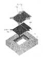
次に、本発明のさらに別の実施形態について図7〜図12を参照して説明する。図7は、本実施形態に係る音響センサ11の概略構成を示す平面図であり、図8は、図7のC−C線で断面し、矢印方向に見た図である。また、図9は、本実施形態の音響センサ11における振動膜22の概略構成を示す平面図である。また、図10は、本実施形態に係る音響センサ11の分解組立図である。なお、図7では、固定膜23の保護膜231は、半導体基板21と設置される輪郭のみ図示されている。[Embodiment 4]
Next, still another embodiment of the present invention will be described with reference to FIGS. FIG. 7 is a plan view showing a schematic configuration of the
図7〜図10に示す音響センサ11は、図5に示す音響センサ11に比べて、振動膜22および固定膜23が、上記基部から側方にさらに延在している点と、固定膜23の固定電極230の分離形状とが異なり、その他の構成は同様である。 The
固定膜23の固定電極230は、周辺電極230bに代えて、上記側方に延在した側方延在部に延在電極230cが設けられている。すなわち、固定電極230は、中央電極230aと延在電極230cとに分割されている。同様に、コンタクト部27b、配線28b、および接続端子29bに代えて、コンタクト部27c、配線28c、および接続端子29cが設けられている。なお、振動電極220は、コンタクト部24および配線25を介して接続端子26に接続されている。 The fixed
振動膜22は、上記基部が上記側方延在部よりも広い。また、振動膜22は、上記基部が、延在部51の先端部における固定部51aにて固定される一方、上記側方延在部が、前後方向の端部52における固定部52aにて固定される。振動膜22の縁で固定されていない箇所は空隙(ベントホール)になっている。すなわち、振動膜22は、上記基部の領域に対する該基部の固定部51aの面積比が、上記側方延在部の領域に対する該側方延在部の固定部52aの面積比よりも小さくなっている。これにより、上記基部は、上記側方延在部よりも大きく変位することになる。なお、図9の例では、前方右側の固定部51aと前方の固定部52aとは接続している。 The base portion of the
図11は、振動膜22に印加される音圧に対する振動膜22の領域ごとの平均変位量の変化をグラフで示している。なお、音圧の単位はPaであり、平均変位量の単位はμmである。同図を参照すると、上記基部の方が上記側方延在部よりも平均変位量が大きいことが理解できる。従って、振動膜22の上記基部と、固定膜23の中央電極230aとによって形成される可変コンデンサは、小さな音を良好に検出できる高感度可変コンデンサとして機能する。 FIG. 11 is a graph showing a change in the average displacement amount for each region of the
また、図11を参照すると、上記基部のグラフでは、音圧に対する平均変位量の傾きは、音圧が120Paに達するまでは一定であるが、音圧が120Paを超えると徐々に小さくなっていることが理解できる。一方、上記側方延在部のグラフでは、音圧に対する平均変位量の傾きは、音圧が200Paに達しても一定であることが理解できる。従って、振動膜22の上記側方延在部と、固定膜23の延在電極230cとによって形成される可変コンデンサは、大きな音を良好に検出できる低感度可変コンデンサとして機能する。 Referring to FIG. 11, in the graph of the base portion, the slope of the average displacement with respect to the sound pressure is constant until the sound pressure reaches 120 Pa, but gradually decreases when the sound pressure exceeds 120 Pa. I understand that. On the other hand, in the graph of the side extension part, it can be understood that the slope of the average displacement with respect to the sound pressure is constant even when the sound pressure reaches 200 Pa. Therefore, the variable capacitor formed by the laterally extending portion of the
また、振動膜22は、固定膜23における中央電極230aおよび延在電極230cの境界領域に対向して、スリット221が形成されている。なお、スリット221は、上記境界領域に対向する領域の一部に形成されているのみであるので、上記基部および上記側方延在部は、物理的および電気的に繋がっている。 In addition, the
ところで、スリット221が形成されていない場合、上記基部と上記側方延在部とは連続しているので、上記基部の変位と上記側方延在部の変位とは互いに影響されることになる。これに対し、本実施形態では、スリット221が形成されているので、上記基部と上記側方延在部とが大部分において分断され、上記基部の変位と上記側方延在部の変位との差がより顕著となる。 By the way, when the
また、開口部31および上記エアギャップの気圧が異なる場合、開口部31および上記エアギャップの一方から他方に、スリット221を介して空気が流れることにより、両者の気圧の差を低減することができる。従って、気圧の変化による音響センサ11の特性の変化を低減することができるとともに、風による雑音など、外部の流体の変化による特性の変化およびノイズなどを低減することができる。 In addition, when the air pressures of the
なお、スリット221の幅が広過ぎると、ベンチレーションの効果が強くなり、スリット221を介しての空気の抜けが大きくなり過ぎて、ロールオフ周波数の低下が発生し、低周波特性が悪化する虞がある。この点について以下に詳述する。 In addition, if the width of the
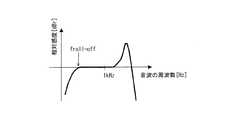
図12は、MEMSマイクロフォンにおける典型的な周波数特性を示している。同図の縦軸は音波の周波数(単位:Hz)であり、横軸は相対感度(単位:dBr)である。同図おいて、グラフが水平である範囲は、上記相対感度が上記音波の周波数に依存しないので、音波を良好に検出できる範囲となる。この範囲の下限の周波数がロールオフ周波数froll−offとなる。FIG. 12 shows a typical frequency characteristic in a MEMS microphone. In the figure, the vertical axis represents the frequency of sound waves (unit: Hz), and the horizontal axis represents relative sensitivity (unit: dBr). In the figure, the range where the graph is horizontal is a range in which sound waves can be detected well because the relative sensitivity does not depend on the frequency of the sound waves. The lower limit frequency of this range is the roll-off frequency froll-off .
一般に、ロールオフ周波数froll−offは、ベンチレーションホールの音響抵抗Rventhollと、バックチャンバ(開口部31)内の空気のコンプライアンス(空気バネ定数)Cbackchamberとに依存し、次式で表される。
froll−off∝1/(Rventholl×Cbackchamber) ・・・(1)。In general, the roll-off frequency froll-off depends on the acoustic resistance Rventhall of the ventilation hole and the compliance (air spring constant) Cbackchamber of the air in the back chamber (opening 31), and is expressed by the following equation. The
froll-off ∝1 / (Rventhole × Cbackchamber ) (1).
音響抵抗Rventhollは、スリット221の長さによっても影響されるが、スリット221の幅が広いと低くなる。従って、上記式(1)より、ロールオフ周波数froll−offが上昇してしまい、その結果、低周波特性が悪化することになる。例えば、スリット221幅が1μmであればロールオフ周波数froll−offは50Hz以下であるが、10μmであれば500Hzにもなる。このため、スリット221幅が10μmを超えると、低周波特性が著しく悪化し、音質が損なわれてしまうことになる。従って、スリット221の幅は10μm以下であることが望ましい。The acoustic resistance Rventroll is also affected by the length of the
〔実施の形態5〕
次に、本発明の他の実施形態について図13および図14を参照して説明する。図13は、本実施形態に係る音響センサ11における振動膜22の概略構成を示す平面図であり、図14は、本実施形態に係る音響センサ11の分解組立図である。[Embodiment 5]
Next, another embodiment of the present invention will be described with reference to FIGS. FIG. 13 is a plan view showing a schematic configuration of the
本実施形態の音響センサ11は、図7〜図10に示す音響センサ11に比べて、固定電極230の中央電極230aおよび延在電極230cが接続されている一方、振動電極220が、上記基部および上記側方延在部にて中央電極220aおよび延在電極220bにそれぞれ分離している点が異なり、その他の構成は同様である。このように、振動電極220を分離することもできる。この場合、中央電極220aおよび延在電極220bが、ASIC12のアンプ121・122に接続されることになる。Compared to the
本発明は上述した各実施形態に限定されるものではなく、請求項に示した範囲で種々の変更が可能であり、異なる実施形態にそれぞれ開示された技術的手段を適宜組み合わせて得られる実施形態についても本発明の技術的範囲に含まれる。 The present invention is not limited to the above-described embodiments, and various modifications are possible within the scope shown in the claims, and embodiments obtained by appropriately combining technical means disclosed in different embodiments. Is also included in the technical scope of the present invention.
例えば、上記実施形態では、音孔部32は、断面が円形であるが、三角形、四角形など、任意の形状にしてもよい。 For example, in the above embodiment, the
また、上記実施形態では、振動電極220および固定電極230の何れか一方を2つに分割しているが、3つ以上に分割してもよい。しかしながら、分割された電極の数が増えると、該電極からの信号を伝達するための配線、ASIC12において上記信号を処理するための電気回路などを増やす必要があり、音響センサ11およびMEMSマイクロフォン10のサイズが増大することになる。従って、上記分割された電極の数は、例えば2など、少ない方が望ましい。 In the above embodiment, either one of the vibrating
また、振動電極220および固定電極230の両方を分割してもよい。この場合、ASIC12のアンプ121・122の特性に応じて、振動電極220および固定電極230の何れか一方の分割された電極をアンプ121・122に接続し、他方の分割された電極を短絡すればよい。もしくは、ASIC12のチャージポンプ120を複数個設け、何れか一方の分割されたそれぞれ電極に接続し、他方の分割された電極にアンプ121・122を接続してもよい。 Further, both the
以上のように、本発明に係る音響トランスデューサは、同じ振動膜および固定膜内に、音波を複数の電気信号に変換できる音響トランスデューサを実現することにより、音響特性のバラツキを抑えることができるので、任意のMEMS型音響センサに適用することができる。 As described above, the acoustic transducer according to the present invention can suppress variations in acoustic characteristics by realizing an acoustic transducer that can convert sound waves into a plurality of electrical signals in the same vibrating membrane and fixed membrane. It can be applied to any MEMS type acoustic sensor.
10 MEMSマイクロフォン
11 音響センサ
12 ASIC
13 配線基板
14 カバー
15 金ワイヤ
16 接続端子
17 貫通孔
21 半導体基板
22 振動膜
23 固定膜
24 コンタクト部
25 配線
26 接続端子
27 コンタクト部
28 配線
29 接続端子
30 絶縁層
31 開口部
32 音孔部
50 隅部
51 延在部
51a 固定部
52 端部
52a 固定部
110 低感度可変コンデンサ
111 高感度可変コンデンサ
120 チャージポンプ
121 低感度用アンプ
122 高感度用アンプ
123・124 ADC
125 バッファ
220 振動電極
220a 中央電極
220b 延在電極
221 スリット
230 固定電極
230a 中央電極
230b 周辺電極
230c 延在電極
231 保護膜
232 突起部10
13
125
Claims (22)
Translated fromJapanese上記基板は、上記上面にて開口した開口部を有しており、
上記振動電極および上記固定電極の少なくとも一方が、上記開口部の上方にて分割されており、
分割された複数の電極から複数の上記電気信号をそれぞれ出力するものであり、
上記振動膜は、矩形である基部と、基部から側方に延在した延在部とを備えており、
上記基部は、4隅にて上記基板または上記固定膜に固定されており、
上記延在部は、2端にて上記基板または上記固定膜に固定されていることを特徴とする音響トランスデューサ。A vibration film and a fixed film are formed on the upper surface of the substrate, and a sound wave is detected and converted into an electric signal and output by a change in capacitance between the vibration electrode in the vibration film and the fixed electrode in the fixed film. In the transducer,
The substrate has an opening opened on the upper surface,
At least one of the vibrating electrode and the fixed electrode is divided above the opening,
A plurality of the electrical signals are respectively output from the plurality of divided electrodes,
The vibration membrane includes a base portion that is rectangular, and an extending portion that extends laterally from the base portion,
The base is fixed to the substrate or the fixing film at four corners,
2. The acoustic transducer according to claim 1, wherein the extending portion is fixed to the substrate or the fixed film at two ends.
上記基板は、上記上面にて開口した開口部を有しており、
上記振動電極および上記固定電極の少なくとも一方が、上記開口部の上方にて分割されており、
分割された複数の電極から複数の上記電気信号をそれぞれ出力するものであり、
上記振動電極および上記固定電極は両方が分割されており、上記振動電極および上記固定電極の一方は、分割された電極が電気的に短絡していることを特徴とする音響トランスデューサ。A vibration film and a fixed film are formed on the upper surface of the substrate, and a sound wave is detected and converted into an electric signal and output by a change in capacitance between the vibration electrode in the vibration film and the fixed electrode in the fixed film. In the transducer,
The substrate has an opening opened on the upper surface,
At least one of the vibrating electrode and the fixed electrode is divided above the opening,
A plurality of the electrical signals are respectively output from the plurality of divided electrodes,
An acoustic transducer characterized in that both the vibration electrode and the fixed electrode are divided, and one of the vibration electrode and the fixed electrode is electrically short-circuited.
該開口部から音波が入射するようになっていることを特徴とする請求項1または2に記載の音響トランスデューサ。The opening is provided in a region facing the central portion of the vibrating membrane,
The acoustic transducer according to claim 1, wherein a sound wave is incident from the opening.
上記音響トランスデューサは、請求項1から21までの何れか1項に記載の音響トランスデューサであることを特徴とするマイクロフォン。A vibration film and a fixed film are formed on the upper surface of the substrate, and a sound wave is detected and converted into an electric signal and output by a change in capacitance between the vibration electrode in the vibration film and the fixed electrode in the fixed film. In a microphone comprising a transducer and an IC that supplies electric power to the acoustic transducer and amplifies an electrical signal from the acoustic transducer and outputs the amplified signal to the outside.
The microphone according to any one of claims 1 to 21, wherein the acoustic transducer is the acoustic transducer according to any one of claims 1 to 21.
Priority Applications (11)
| Application Number | Priority Date | Filing Date | Title |
|---|---|---|---|
| JP2011002313AJP5872163B2 (en) | 2011-01-07 | 2011-01-07 | Acoustic transducer and microphone using the acoustic transducer |
| KR1020137017482AKR101512583B1 (en) | 2011-01-07 | 2011-12-22 | Sound transducer and microphone using same |
| EP11854547.4AEP2663093B1 (en) | 2011-01-07 | 2011-12-22 | Sound transducer and microphone using same |
| US13/978,531US9936305B2 (en) | 2011-01-07 | 2011-12-22 | Acoustic transducer and microphone using the acoustic transducer |
| PCT/JP2011/079843WO2012093598A1 (en) | 2011-01-07 | 2011-12-22 | Sound transducer and microphone using same |
| CN201180064105.8ACN103329575B (en) | 2011-01-07 | 2011-12-22 | Acoustic transducer and use the mike of this acoustic transducer |
| US13/936,104US9363608B2 (en) | 2011-01-07 | 2013-07-05 | Acoustic transducer |
| US13/936,110US9380380B2 (en) | 2011-01-07 | 2013-07-05 | Acoustic transducer and interface circuit |
| US15/017,514US9843868B2 (en) | 2011-01-07 | 2016-02-05 | Acoustic transducer |
| US15/814,256US10405107B2 (en) | 2011-01-07 | 2017-11-15 | Acoustic transducer |
| US15/904,209US10484798B2 (en) | 2011-01-07 | 2018-02-23 | Acoustic transducer and microphone using the acoustic transducer |
Applications Claiming Priority (1)
| Application Number | Priority Date | Filing Date | Title |
|---|---|---|---|
| JP2011002313AJP5872163B2 (en) | 2011-01-07 | 2011-01-07 | Acoustic transducer and microphone using the acoustic transducer |
Publications (3)
| Publication Number | Publication Date |
|---|---|
| JP2012147115A JP2012147115A (en) | 2012-08-02 |
| JP2012147115A5 JP2012147115A5 (en) | 2013-10-31 |
| JP5872163B2true JP5872163B2 (en) | 2016-03-01 |
Family
ID=46457458
Family Applications (1)
| Application Number | Title | Priority Date | Filing Date |
|---|---|---|---|
| JP2011002313AActiveJP5872163B2 (en) | 2011-01-07 | 2011-01-07 | Acoustic transducer and microphone using the acoustic transducer |
Country Status (6)
| Country | Link |
|---|---|
| US (5) | US9936305B2 (en) |
| EP (1) | EP2663093B1 (en) |
| JP (1) | JP5872163B2 (en) |
| KR (1) | KR101512583B1 (en) |
| CN (1) | CN103329575B (en) |
| WO (1) | WO2012093598A1 (en) |
Families Citing this family (46)
| Publication number | Priority date | Publication date | Assignee | Title |
|---|---|---|---|---|
| JP5872163B2 (en)* | 2011-01-07 | 2016-03-01 | オムロン株式会社 | Acoustic transducer and microphone using the acoustic transducer |
| US9380380B2 (en) | 2011-01-07 | 2016-06-28 | Stmicroelectronics S.R.L. | Acoustic transducer and interface circuit |
| ITTO20120987A1 (en) | 2012-11-14 | 2014-05-15 | St Microelectronics Srl | DIGITAL INTERFACE ELECTRONIC CIRCUIT FOR AN ACOUSTIC TRANSDUCER AND ITS ACOUSTIC TRANSDUCTION SYSTEM |
| US9454954B2 (en)* | 2012-05-01 | 2016-09-27 | Fujifilm Dimatix, Inc. | Ultra wide bandwidth transducer with dual electrode |
| US8767512B2 (en) | 2012-05-01 | 2014-07-01 | Fujifilm Dimatix, Inc. | Multi-frequency ultra wide bandwidth transducer |
| JP6028479B2 (en) | 2012-09-14 | 2016-11-16 | オムロン株式会社 | Capacitive sensor, acoustic sensor and microphone |
| US9804003B2 (en)* | 2012-10-23 | 2017-10-31 | Apple Inc. | Electronic devices with environmental sensors |
| US9660170B2 (en) | 2012-10-26 | 2017-05-23 | Fujifilm Dimatix, Inc. | Micromachined ultrasonic transducer arrays with multiple harmonic modes |
| TWM457365U (en)* | 2012-11-09 | 2013-07-11 | Raytrend Technology Corp | Electrostatic loudspeaker with multi-channel |
| US9407231B2 (en) | 2013-02-06 | 2016-08-02 | Htc Corporation | Apparatus and method of multi-sensor sound recording |
| JP6237978B2 (en) | 2013-03-13 | 2017-11-29 | オムロン株式会社 | Capacitive sensor, acoustic sensor and microphone |
| US9681234B2 (en)* | 2013-05-09 | 2017-06-13 | Shanghai Ic R&D Center Co., Ltd | MEMS microphone structure and method of manufacturing the same |
| JP6179300B2 (en) | 2013-09-13 | 2017-08-16 | オムロン株式会社 | Acoustic transducer and microphone |
| JP6179297B2 (en) | 2013-09-13 | 2017-08-16 | オムロン株式会社 | Acoustic transducer and microphone |
| ITTO20130901A1 (en) | 2013-11-05 | 2015-05-06 | St Microelectronics Srl | EXPANSION INTERFACE OF THE DYNAMIC INTERVAL OF AN INPUT SIGNAL, IN PARTICULAR OF AN AUDIO SIGNAL OF AN ACOUSTIC TRANSDUCER WITH TWO DETECTION STRUCTURES, AND RELATIVE METHOD |
| US20150208165A1 (en)* | 2014-01-21 | 2015-07-23 | Knowles Electronics, Llc | Microphone Apparatus and Method To Provide Extremely High Acoustic Overload Points |
| US9609410B2 (en) | 2014-02-20 | 2017-03-28 | Stmicroelectronics S.R.L. | Processing circuit for a multiple sensing structure digital microelectromechanical sensor having a broad dynamic range and sensor comprising the processing circuit |
| US9344808B2 (en)* | 2014-03-18 | 2016-05-17 | Invensense, Inc. | Differential sensing acoustic sensor |
| US10142729B2 (en) | 2014-05-20 | 2018-11-27 | Tdk Corporation | Microphone and method of operating a microphone |
| US11619983B2 (en)* | 2014-09-15 | 2023-04-04 | Qeexo, Co. | Method and apparatus for resolving touch screen ambiguities |
| KR101550636B1 (en) | 2014-09-23 | 2015-09-07 | 현대자동차 주식회사 | Micro phone and method manufacturing the same |
| JP6390423B2 (en)* | 2014-12-26 | 2018-09-19 | オムロン株式会社 | Acoustic sensor and acoustic sensor manufacturing method |
| CN204408625U (en)* | 2015-01-21 | 2015-06-17 | 瑞声声学科技(深圳)有限公司 | Mems microphone |
| WO2016118351A1 (en)* | 2015-01-22 | 2016-07-28 | The Board Of Trustees Of The University Of Illinois | Micro-electro-mechanical-systems based acoustic emission sensors |
| JP6432372B2 (en)* | 2015-02-02 | 2018-12-05 | オムロン株式会社 | Acoustic sensor |
| KR101638730B1 (en) | 2015-02-10 | 2016-07-12 | 경북대학교 산학협력단 | Ultrasonic transducer, ultrasonic device including the same and method for manufacturing the same |
| WO2016153851A1 (en)* | 2015-03-20 | 2016-09-29 | Knowles Electronics, Llc | Acoustic device with one or more trim capacitors |
| US10291973B2 (en)* | 2015-05-14 | 2019-05-14 | Knowles Electronics, Llc | Sensor device with ingress protection |
| US9807532B2 (en)* | 2015-05-22 | 2017-10-31 | Kathirgamasundaram Sooriakumar | Acoustic apparatus, system and method of fabrication |
| CN106197776B (en) | 2015-05-27 | 2019-11-05 | 意法半导体股份有限公司 | Pressure sensor, pressure measuring device, braking system and the method for measuring pressure |
| US9560455B2 (en) | 2015-06-26 | 2017-01-31 | Stmicroelectronics S.R.L. | Offset calibration in a multiple membrane microphone |
| US9752900B2 (en)* | 2015-07-10 | 2017-09-05 | Wyrobek International, Inc. | Multi-plate capacitive transducer |
| US10003889B2 (en) | 2015-08-04 | 2018-06-19 | Infineon Technologies Ag | System and method for a multi-electrode MEMS device |
| RU2619807C1 (en)* | 2016-03-04 | 2017-05-18 | Акционерное общество "Творческо-производственное объединение "Центральная киностудия детских и юношеских фильмов им. М. Горького" | Condenser microphone capsules |
| US9731965B1 (en) | 2016-03-31 | 2017-08-15 | Stmicroelectronics S.R.L. | Dry scribing methods, devices and systems |
| US10153740B2 (en)* | 2016-07-11 | 2018-12-11 | Knowles Electronics, Llc | Split signal differential MEMS microphone |
| KR101916052B1 (en) | 2016-09-09 | 2018-11-07 | 현대자동차 주식회사 | Microphone, manufacturing method and control method therefor |
| IT201600121533A1 (en) | 2016-11-30 | 2018-05-30 | St Microelectronics Srl | MEMS INTEGRATED ELECTROACOUSTIC TRANSDUCER WITH IMPROVED SENSITIVITY AND RELATIVE PROCESS OF MANUFACTURING |
| DE102017206744B9 (en) | 2017-04-21 | 2023-01-12 | Infineon Technologies Ag | HIGH THERMAL CAPACITY MEMS PACKAGE AND METHOD OF MAKING SAME |
| US10361145B2 (en)* | 2017-07-18 | 2019-07-23 | Skyworks Solutions, Inc. | Through-mold openings for dual-sided packaged modules with ball grid arrays |
| US10718801B2 (en) | 2017-08-21 | 2020-07-21 | Cirrus Logic, Inc. | Reducing noise in a capacitive sensor with a pulse density modulator |
| JP1602867S (en)* | 2017-08-24 | 2018-05-07 | ||
| US10917727B2 (en)* | 2018-03-16 | 2021-02-09 | Vesper Technologies, Inc. | Transducer system with configurable acoustic overload point |
| US11902727B2 (en)* | 2022-02-11 | 2024-02-13 | Apple Inc. | Inductive acoustic filters for acoustic devices |
| TWI818600B (en)* | 2022-06-27 | 2023-10-11 | 國立臺灣大學 | Piezoelectric units for piezoelectric speakers |
| WO2024223318A1 (en)* | 2023-04-24 | 2024-10-31 | Philip Morris Products S.A. | Improved youth access prevention for aerosol-generating devices |
Family Cites Families (101)
| Publication number | Priority date | Publication date | Assignee | Title |
|---|---|---|---|---|
| US3588382A (en) | 1967-10-11 | 1971-06-28 | Northern Electric Co | Directional electret transducer |
| CH533408A (en) | 1972-02-02 | 1973-01-31 | Bommer Ag | Hearing aid |
| SE438233B (en)* | 1983-08-19 | 1985-04-01 | Ericsson Telefon Ab L M | electret |
| SU1582361A1 (en) | 1985-05-06 | 1990-07-30 | Предприятие П/Я Р-6947 | Microphone with variable sensitivity |
| JPS62213400A (en)* | 1986-03-13 | 1987-09-19 | Sony Corp | Capacitor type microphone |
| JPH0726887B2 (en) | 1986-05-31 | 1995-03-29 | 株式会社堀場製作所 | Condenser Microphone type detector diaphragm |
| DK155269C (en) | 1986-07-17 | 1989-07-24 | Brueel & Kjaer As | Pressure gradient |
| SU1670807A1 (en) | 1989-01-09 | 1991-08-15 | Предприятие П/Я Р-6947 | Capacitor microphone |
| JPH03139097A (en) | 1989-10-25 | 1991-06-13 | Hitachi Ltd | Microphone pickup method |
| US5388163A (en) | 1991-12-23 | 1995-02-07 | At&T Corp. | Electret transducer array and fabrication technique |
| US5524056A (en) | 1993-04-13 | 1996-06-04 | Etymotic Research, Inc. | Hearing aid having plural microphones and a microphone switching system |
| DE4342169A1 (en)* | 1993-12-10 | 1995-06-14 | Sennheiser Electronic | Electromechanical converter such as microphone |
| US5452268A (en) | 1994-08-12 | 1995-09-19 | The Charles Stark Draper Laboratory, Inc. | Acoustic transducer with improved low frequency response |
| US5517683A (en) | 1995-01-18 | 1996-05-14 | Cycomm Corporation | Conformant compact portable cellular phone case system and connector |
| EP0766494B1 (en) | 1995-09-29 | 2002-08-14 | STMicroelectronics S.r.l. | Digital microphonic device |
| JPH10126886A (en)* | 1996-10-21 | 1998-05-15 | Hirahiro Toshimitsu | Digital electroacoustic transducer |
| US5982709A (en) | 1998-03-31 | 1999-11-09 | The Board Of Trustees Of The Leland Stanford Junior University | Acoustic transducers and method of microfabrication |
| US6271780B1 (en) | 1998-10-08 | 2001-08-07 | Cirrus Logic, Inc. | Gain ranging analog-to-digital converter with error correction |
| US7003127B1 (en) | 1999-01-07 | 2006-02-21 | Sarnoff Corporation | Hearing aid with large diaphragm microphone element including a printed circuit board |
| EP1172020B1 (en) | 1999-02-05 | 2006-09-06 | Hearworks Pty Ltd. | Adaptive dynamic range optimisation sound processor |
| GB2351169B (en) | 1999-06-14 | 2003-11-19 | Nokia Mobile Phones Ltd | Audio apparatus |
| US6882734B2 (en) | 2001-02-14 | 2005-04-19 | Gentex Corporation | Vehicle accessory microphone |
| US6449593B1 (en) | 2000-01-13 | 2002-09-10 | Nokia Mobile Phones Ltd. | Method and system for tracking human speakers |
| CN1470147A (en) | 2000-08-07 | 2004-01-21 | �µ��ǿƼ��ɷ���������˾ | Method and apparatus for filtering & compressing sound signals |
| US6535460B2 (en) | 2000-08-11 | 2003-03-18 | Knowles Electronics, Llc | Miniature broadband acoustic transducer |
| JP4296731B2 (en)* | 2001-07-18 | 2009-07-15 | 株式会社デンソー | Manufacturing method of capacitive pressure sensor |
| US6944474B2 (en) | 2001-09-20 | 2005-09-13 | Sound Id | Sound enhancement for mobile phones and other products producing personalized audio for users |
| AU2002365352A1 (en) | 2001-11-27 | 2003-06-10 | Corporation For National Research Initiatives | A miniature condenser microphone and fabrication method therefor |
| WO2003059010A1 (en) | 2002-01-12 | 2003-07-17 | Oticon A/S | Wind noise insensitive hearing aid |
| US20030210799A1 (en) | 2002-05-10 | 2003-11-13 | Gabriel Kaigham J. | Multiple membrane structure and method of manufacture |
| EP1385324A1 (en) | 2002-07-22 | 2004-01-28 | Siemens Aktiengesellschaft | A system and method for reducing the effect of background noise |
| KR20050071584A (en) | 2002-10-17 | 2005-07-07 | 코닌클리케 필립스 일렉트로닉스 엔.브이. | Means for limiting an output signal of an amplifier stage |
| US7359504B1 (en) | 2002-12-03 | 2008-04-15 | Plantronics, Inc. | Method and apparatus for reducing echo and noise |
| JP4311034B2 (en) | 2003-02-14 | 2009-08-12 | 沖電気工業株式会社 | Band restoration device and telephone |
| DE10313330B4 (en) | 2003-03-25 | 2005-04-14 | Siemens Audiologische Technik Gmbh | Method for suppressing at least one acoustic interference signal and apparatus for carrying out the method |
| DK1627553T3 (en) | 2003-05-19 | 2008-04-28 | Widex As | A hearing aid |
| JP4101785B2 (en) | 2003-09-11 | 2008-06-18 | アオイ電子株式会社 | Condenser microphone and manufacturing method thereof |
| DE102004010863B3 (en) | 2004-03-05 | 2005-10-20 | Siemens Audiologische Technik | Hearing aid with several microphones |
| WO2006007441A1 (en) | 2004-06-16 | 2006-01-19 | Cardo Systems Inc. | Wireless communication headset with microphone switching system |
| JP4585825B2 (en)* | 2004-09-30 | 2010-11-24 | 株式会社オーディオテクニカ | Condenser microphone |
| US7346178B2 (en) | 2004-10-29 | 2008-03-18 | Silicon Matrix Pte. Ltd. | Backplateless silicon microphone |
| JP4539450B2 (en) | 2004-11-04 | 2010-09-08 | オムロン株式会社 | Capacitive vibration sensor and manufacturing method thereof |
| FR2884101B1 (en) | 2005-03-30 | 2007-06-29 | Merry Electronics Co Ltd | SILICON MICROPHONE CAPACITOR WITH MINIMAL DIAPHRAGM EFFORT |
| EP1732352B1 (en) | 2005-04-29 | 2015-10-21 | Nuance Communications, Inc. | Detection and suppression of wind noise in microphone signals |
| WO2006123263A1 (en) | 2005-05-17 | 2006-11-23 | Nxp B.V. | Improved membrane for a mems condenser microphone |
| JP4641217B2 (en)* | 2005-06-08 | 2011-03-02 | 株式会社豊田中央研究所 | Microphone and manufacturing method thereof |
| DE102005032292B3 (en) | 2005-07-11 | 2006-09-21 | Siemens Audiologische Technik Gmbh | Hearing aid for directional hearing has noise detection device to detect noise level of microphones whereby two noise levels can be compared with one another and appropriate control pulse can be displayed at microphone device |
| KR101228383B1 (en) | 2005-07-22 | 2013-02-07 | 에스티마이크로일렉트로닉스 에스.알.엘. | Integrated pressure sensor with double measuring scale and a high full-scale value |
| SG130158A1 (en) | 2005-08-20 | 2007-03-20 | Bse Co Ltd | Silicon based condenser microphone and packaging method for the same |
| WO2007024909A1 (en) | 2005-08-23 | 2007-03-01 | Analog Devices, Inc. | Multi-microphone system |
| JP4535046B2 (en) | 2006-08-22 | 2010-09-01 | ヤマハ株式会社 | Capacitance sensor and manufacturing method thereof |
| US20070121972A1 (en) | 2005-09-26 | 2007-05-31 | Yamaha Corporation | Capacitor microphone and diaphragm therefor |
| US7856283B2 (en) | 2005-12-13 | 2010-12-21 | Sigmatel, Inc. | Digital microphone interface, audio codec and methods for use therewith |
| US7836770B2 (en) | 2005-12-20 | 2010-11-23 | Etymotic Research, Inc. | Method and system for noise dosimeter with quick-check mode and earphone adapter |
| DE102006004287A1 (en) | 2006-01-31 | 2007-08-02 | Robert Bosch Gmbh | Micro mechanical structure used in microphones has rings of flexible electrode segments |
| TW200738028A (en) | 2006-02-24 | 2007-10-01 | Yamaha Corp | Condenser microphone |
| TW200746868A (en) | 2006-02-24 | 2007-12-16 | Yamaha Corp | Condenser microphone |
| US7676052B1 (en) | 2006-02-28 | 2010-03-09 | National Semiconductor Corporation | Differential microphone assembly |
| GB0605576D0 (en) | 2006-03-20 | 2006-04-26 | Oligon Ltd | MEMS device |
| JP4770605B2 (en) | 2006-06-26 | 2011-09-14 | ヤマハ株式会社 | Balanced output microphone and method of manufacturing balanced output microphone |
| EP2044802B1 (en) | 2006-07-25 | 2013-03-27 | Analog Devices, Inc. | Multiple microphone system |
| US7804969B2 (en) | 2006-08-07 | 2010-09-28 | Shandong Gettop Acoustic Co., Ltd. | Silicon microphone with impact proof structure |
| KR100892095B1 (en) | 2007-01-23 | 2009-04-06 | 삼성전자주식회사 | Transmission and reception voice signal processing apparatus and method in a headset |
| US20080192963A1 (en) | 2007-02-09 | 2008-08-14 | Yamaha Corporation | Condenser microphone |
| JP2008199226A (en)* | 2007-02-09 | 2008-08-28 | Yamaha Corp | Condenser microphone device |
| US20080192962A1 (en) | 2007-02-13 | 2008-08-14 | Sonion Nederland B.V. | Microphone with dual transducers |
| US8644528B2 (en) | 2007-02-20 | 2014-02-04 | Case Western Reserve University | Microfabricated microphone |
| TW200904222A (en) | 2007-02-26 | 2009-01-16 | Yamaha Corp | Sensitive silicon microphone with wide dynamic range |
| JP2008263498A (en) | 2007-04-13 | 2008-10-30 | Sanyo Electric Co Ltd | Wind noise reducing device, sound signal recorder and imaging apparatus |
| CN101346014B (en) | 2007-07-13 | 2012-06-20 | 清华大学 | Micro electro-mechanical system microphone and preparation method thereof |
| JP2009028808A (en) | 2007-07-24 | 2009-02-12 | Rohm Co Ltd | Mems sensor and manufacturing method of mems sensor |
| JP2009081624A (en) | 2007-09-26 | 2009-04-16 | Rohm Co Ltd | Semiconductor sensor device |
| US8045733B2 (en) | 2007-10-05 | 2011-10-25 | Shandong Gettop Acoustic Co., Ltd. | Silicon microphone with enhanced impact proof structure using bonding wires |
| US20090095081A1 (en) | 2007-10-16 | 2009-04-16 | Rohm Co., Ltd. | Semiconductor device |
| JP2009098022A (en)* | 2007-10-17 | 2009-05-07 | Rohm Co Ltd | Semiconductor device |
| JP4946796B2 (en) | 2007-10-29 | 2012-06-06 | ヤマハ株式会社 | Vibration transducer and method of manufacturing vibration transducer |
| JP2009124474A (en) | 2007-11-15 | 2009-06-04 | Yamaha Corp | Electrostatic speaker |
| US8467559B2 (en) | 2008-02-20 | 2013-06-18 | Shandong Gettop Acoustic Co., Ltd. | Silicon microphone without dedicated backplate |
| CN101785325B (en)* | 2008-02-20 | 2013-07-17 | 欧姆龙株式会社 | Electrostatic capacitive vibrating sensor |
| US8223981B2 (en) | 2008-05-23 | 2012-07-17 | Analog Devices, Inc. | Wide dynamic range microphone |
| JP5006364B2 (en) | 2008-07-28 | 2012-08-22 | アオイ電子株式会社 | Directional microphone |
| JP4419103B1 (en) | 2008-08-27 | 2010-02-24 | オムロン株式会社 | Capacitance type vibration sensor |
| US20100117485A1 (en) | 2008-11-13 | 2010-05-13 | Avago Technologies Wireless Ip (Singapore) Pte. Ltd. | Piezoelectric transducers with noise-cancelling electrodes |
| US8284958B2 (en) | 2008-12-22 | 2012-10-09 | Nokia Corporation | Increased dynamic range microphone |
| IT1395550B1 (en) | 2008-12-23 | 2012-09-28 | St Microelectronics Rousset | INTEGRATED ACOUSTIC TRANSDUCER IN MEMS TECHNOLOGY AND RELATIVE PROCESS OF PROCESSING |
| IT1392742B1 (en) | 2008-12-23 | 2012-03-16 | St Microelectronics Rousset | INTEGRATED ACOUSTIC TRANSDUCER IN MEMS TECHNOLOGY AND RELATIVE PROCESS OF PROCESSING |
| US8233637B2 (en) | 2009-01-20 | 2012-07-31 | Nokia Corporation | Multi-membrane microphone for high-amplitude audio capture |
| US8175293B2 (en) | 2009-04-16 | 2012-05-08 | Nokia Corporation | Apparatus, methods and computer programs for converting sound waves to electrical signals |
| EP2252077B1 (en) | 2009-05-11 | 2012-07-11 | STMicroelectronics Srl | Assembly of a capacitive acoustic transducer of the microelectromechanical type and package thereof |
| JP5491080B2 (en)* | 2009-06-18 | 2014-05-14 | 国立大学法人 東京大学 | microphone |
| KR20130137050A (en) | 2009-06-29 | 2013-12-13 | 노키아 코포레이션 | Temperature compensated microphone |
| JP5588745B2 (en) | 2010-05-27 | 2014-09-10 | オムロン株式会社 | Acoustic transducer and microphone using the acoustic transducer |
| CN103155032B (en) | 2010-08-27 | 2016-10-19 | 诺基亚技术有限公司 | Microphone device and method for removing unwanted sound |
| TWI437555B (en) | 2010-10-19 | 2014-05-11 | Univ Nat Chiao Tung | A spatially pre-processed target-to-jammer ratio weighted filter and method thereof |
| JP5872163B2 (en) | 2011-01-07 | 2016-03-01 | オムロン株式会社 | Acoustic transducer and microphone using the acoustic transducer |
| ITTO20120987A1 (en) | 2012-11-14 | 2014-05-15 | St Microelectronics Srl | DIGITAL INTERFACE ELECTRONIC CIRCUIT FOR AN ACOUSTIC TRANSDUCER AND ITS ACOUSTIC TRANSDUCTION SYSTEM |
| US9380380B2 (en) | 2011-01-07 | 2016-06-28 | Stmicroelectronics S.R.L. | Acoustic transducer and interface circuit |
| US8351625B2 (en) | 2011-02-23 | 2013-01-08 | Omron Corporation | Acoustic sensor and microphone |
| US9036838B2 (en) | 2013-07-11 | 2015-05-19 | Merry Electronics (Shenzhen) Co., Ltd. | Dual-diaphragm acoustic transducer |
| US8934649B1 (en) | 2013-08-29 | 2015-01-13 | Solid State System Co., Ltd. | Micro electro-mechanical system (MEMS) microphone device with multi-sensitivity outputs and circuit with the MEMS device |
| JP6179300B2 (en) | 2013-09-13 | 2017-08-16 | オムロン株式会社 | Acoustic transducer and microphone |
- 2011
- 2011-01-07JPJP2011002313Apatent/JP5872163B2/enactiveActive
- 2011-12-22EPEP11854547.4Apatent/EP2663093B1/enactiveActive
- 2011-12-22KRKR1020137017482Apatent/KR101512583B1/ennot_activeExpired - Fee Related
- 2011-12-22WOPCT/JP2011/079843patent/WO2012093598A1/enactiveApplication Filing
- 2011-12-22CNCN201180064105.8Apatent/CN103329575B/enactiveActive
- 2011-12-22USUS13/978,531patent/US9936305B2/enactiveActive
- 2013
- 2013-07-05USUS13/936,104patent/US9363608B2/enactiveActive
- 2016
- 2016-02-05USUS15/017,514patent/US9843868B2/enactiveActive
- 2017
- 2017-11-15USUS15/814,256patent/US10405107B2/enactiveActive
- 2018
- 2018-02-23USUS15/904,209patent/US10484798B2/enactiveActive
Also Published As
| Publication number | Publication date |
|---|---|
| EP2663093B1 (en) | 2019-06-26 |
| CN103329575B (en) | 2016-08-10 |
| EP2663093A1 (en) | 2013-11-13 |
| WO2012093598A1 (en) | 2012-07-12 |
| US20130294622A1 (en) | 2013-11-07 |
| US20140191343A1 (en) | 2014-07-10 |
| KR101512583B1 (en) | 2015-04-15 |
| US20180295454A1 (en) | 2018-10-11 |
| US20160157023A1 (en) | 2016-06-02 |
| US10484798B2 (en) | 2019-11-19 |
| US9936305B2 (en) | 2018-04-03 |
| US9843868B2 (en) | 2017-12-12 |
| JP2012147115A (en) | 2012-08-02 |
| KR20130091773A (en) | 2013-08-19 |
| CN103329575A (en) | 2013-09-25 |
| US9363608B2 (en) | 2016-06-07 |
| EP2663093A4 (en) | 2016-07-13 |
| US10405107B2 (en) | 2019-09-03 |
| US20180176693A1 (en) | 2018-06-21 |
Similar Documents
| Publication | Publication Date | Title |
|---|---|---|
| JP5872163B2 (en) | Acoustic transducer and microphone using the acoustic transducer | |
| JP5252104B1 (en) | Capacitive sensor, acoustic sensor and microphone | |
| US9380380B2 (en) | Acoustic transducer and interface circuit | |
| JP6237978B2 (en) | Capacitive sensor, acoustic sensor and microphone | |
| US9374644B2 (en) | Acoustic transducer and microphone | |
| JP6028479B2 (en) | Capacitive sensor, acoustic sensor and microphone | |
| JP5928163B2 (en) | Capacitive sensor, acoustic sensor and microphone | |
| US9439002B2 (en) | Integrated package forming wide sense gap micro electro-mechanical system microphone and methodologies for fabricating the same | |
| WO2011148778A1 (en) | Acoustic transducer, and microphone using the acoustic transducer | |
| US10158943B2 (en) | Apparatus and method to bias MEMS motors | |
| US20130136292A1 (en) | Microphone unit | |
| JP2006325034A (en) | Acoustic sensor |
Legal Events
| Date | Code | Title | Description |
|---|---|---|---|
| A521 | Request for written amendment filed | Free format text:JAPANESE INTERMEDIATE CODE: A523 Effective date:20130917 | |
| A621 | Written request for application examination | Free format text:JAPANESE INTERMEDIATE CODE: A621 Effective date:20130917 | |
| A131 | Notification of reasons for refusal | Free format text:JAPANESE INTERMEDIATE CODE: A131 Effective date:20140902 | |
| A521 | Request for written amendment filed | Free format text:JAPANESE INTERMEDIATE CODE: A523 Effective date:20141202 | |
| A131 | Notification of reasons for refusal | Free format text:JAPANESE INTERMEDIATE CODE: A131 Effective date:20150602 | |
| A521 | Request for written amendment filed | Free format text:JAPANESE INTERMEDIATE CODE: A523 Effective date:20150731 | |
| RD04 | Notification of resignation of power of attorney | Free format text:JAPANESE INTERMEDIATE CODE: A7424 Effective date:20151023 | |
| RD03 | Notification of appointment of power of attorney | Free format text:JAPANESE INTERMEDIATE CODE: A7423 Effective date:20151028 | |
| A521 | Request for written amendment filed | Free format text:JAPANESE INTERMEDIATE CODE: A523 Effective date:20151113 | |
| TRDD | Decision of grant or rejection written | ||
| A01 | Written decision to grant a patent or to grant a registration (utility model) | Free format text:JAPANESE INTERMEDIATE CODE: A01 Effective date:20151215 | |
| A61 | First payment of annual fees (during grant procedure) | Free format text:JAPANESE INTERMEDIATE CODE: A61 Effective date:20160113 | |
| R150 | Certificate of patent or registration of utility model | Ref document number:5872163 Country of ref document:JP Free format text:JAPANESE INTERMEDIATE CODE: R150 | |
| RD04 | Notification of resignation of power of attorney | Free format text:JAPANESE INTERMEDIATE CODE: R3D04 | |
| RD04 | Notification of resignation of power of attorney | Free format text:JAPANESE INTERMEDIATE CODE: R3D04 | |
| R250 | Receipt of annual fees | Free format text:JAPANESE INTERMEDIATE CODE: R250 | |
| R250 | Receipt of annual fees | Free format text:JAPANESE INTERMEDIATE CODE: R250 | |
| R250 | Receipt of annual fees | Free format text:JAPANESE INTERMEDIATE CODE: R250 | |
| S111 | Request for change of ownership or part of ownership | Free format text:JAPANESE INTERMEDIATE CODE: R313115 | |
| R350 | Written notification of registration of transfer | Free format text:JAPANESE INTERMEDIATE CODE: R350 | |
| R250 | Receipt of annual fees | Free format text:JAPANESE INTERMEDIATE CODE: R250 | |
| R250 | Receipt of annual fees | Free format text:JAPANESE INTERMEDIATE CODE: R250 | |
| R250 | Receipt of annual fees | Free format text:JAPANESE INTERMEDIATE CODE: R250 |