JP5871889B2 - LED lamp and LED lighting system - Google Patents
LED lamp and LED lighting systemDownload PDFInfo
- Publication number
- JP5871889B2 JP5871889B2JP2013255562AJP2013255562AJP5871889B2JP 5871889 B2JP5871889 B2JP 5871889B2JP 2013255562 AJP2013255562 AJP 2013255562AJP 2013255562 AJP2013255562 AJP 2013255562AJP 5871889 B2JP5871889 B2JP 5871889B2
- Authority
- JP
- Japan
- Prior art keywords
- lighting device
- led
- voltage
- led lamp
- output
- Prior art date
- Legal status (The legal status is an assumption and is not a legal conclusion. Google has not performed a legal analysis and makes no representation as to the accuracy of the status listed.)
- Active
Links
- 238000001514detection methodMethods0.000claimsdescription42
- 238000005259measurementMethods0.000claimsdescription40
- 230000002159abnormal effectEffects0.000claimsdescription9
- 230000000903blocking effectEffects0.000description24
- 238000010586diagramMethods0.000description23
- 239000003990capacitorSubstances0.000description16
- 230000007274generation of a signal involved in cell-cell signalingEffects0.000description13
- 239000000779smokeSubstances0.000description12
- 230000001681protective effectEffects0.000description8
- 230000020169heat generationEffects0.000description6
- 206010011906DeathDiseases0.000description4
- 238000005286illuminationMethods0.000description4
- 238000006243chemical reactionMethods0.000description3
- 238000000034methodMethods0.000description3
- 206010037660PyrexiaDiseases0.000description2
- 230000005856abnormalityEffects0.000description2
- 238000010438heat treatmentMethods0.000description2
- WABPQHHGFIMREM-UHFFFAOYSA-Nlead(0)Chemical compound[Pb]WABPQHHGFIMREM-UHFFFAOYSA-N0.000description2
- 239000002184metalSubstances0.000description2
- 230000001052transient effectEffects0.000description2
- 230000015556catabolic processEffects0.000description1
- 238000009499grossingMethods0.000description1
- 238000003780insertionMethods0.000description1
- 230000037431insertionEffects0.000description1
- 238000004904shorteningMethods0.000description1
Images


Landscapes
- Arrangement Of Elements, Cooling, Sealing, Or The Like Of Lighting Devices (AREA)
- Non-Portable Lighting Devices Or Systems Thereof (AREA)
- Circuit Arrangement For Electric Light Sources In General (AREA)
Description
Translated fromJapanese本発明は、既存の直管蛍光ランプ用照明器具に、LED(発光ダイオード)用点灯装置を付加し、既存のソケットにLEDランプを装着するタイプのLED照明システムに関する。また、そのLED照明システムを構成するLEDランプ及びLED用点灯装置に関する。 The present invention relates to an LED lighting system of a type in which an LED (light emitting diode) lighting device is added to an existing straight tube fluorescent lamp lighting fixture, and an LED lamp is mounted on an existing socket. Moreover, it is related with the LED lamp which comprises the LED illumination system, and the lighting device for LED.
図14は、例えば、特許文献1もしくは特許文献2等に記載された従来のLED照明システム400を示す図である。図14に示すように、従来のLED照明システム400は、既存の直管蛍光ランプ用照明器具401(単に照明器具と呼ぶ場合もある)の安定器402(蛍光ランプ用点灯装置)を取り外し、代わりにLED用点灯装置403を装着する。また、配線についても、安定器402への商用電源からの入力電線404と、安定器402から両端の二つのソケット405への出力電線406をそのままLED用点灯装置403へ接続する。さらに、従来のLED照明システム400は、LED(発光ダイオード)を備え、直管蛍光ランプの全長と、端部構造(口金、口金ピン等)、寸法などを合わせ、さらに全体を類似の形状にすることによって、両端の二つのソケット205に装着できるようにしたLEDランプ407(以下、単にランプと呼ぶ場合もある)をソケット405間に装着する。 FIG. 14 is a diagram illustrating a conventional
商用電源からの入力電線404を介して、LED用点灯装置403に所定の電圧が印加されると、LED用点灯装置403から出力電線406、両端のソケット405を介して、LEDランプ407の両端の口金407a,407bへ電力が供給され、装着されたLEDが発光し、照明に使われる。 When a predetermined voltage is applied to the
尚、特許文献1では、ソケット405と口金407a,407bとの間に識別用のアダプタを設けている。このアダプタは、現行の直管蛍光ランプと識別するために挿入される。 In
また、特許文献2では、口金407a,407bを絶縁し、口金407a,407bはLEDランプ407の支持のみに用い、別にリード線を設けてLED用点灯装置403とLEDランプ407を電気的に接続している。 In
尚、直管蛍光ランプは、両端に設けたフィラメントのさらに両端を独立に安定器402(蛍光ランプ用点灯装置)と接続しなくてはならないため、出力電線406、ソケット405の端子とも、片側2本あるいは2個、両側あわせて4本、あるいは4個必要である。 In the straight tube fluorescent lamp, since both ends of the filaments provided at both ends must be independently connected to the ballast 402 (fluorescent lamp lighting device), both the output
一方、LEDランプ407においては、本来は独立した接続は2個でよい。しかし、図14のLEDランプ407は、直管蛍光ランプと端部構造(口金、口金ピン等)を合わせて構成されているが、例えば、片側2本の口金ピンのうち1本はダミーの口金ピンである。従って、LEDランプ407を、片側2本あるいは2個、両側あわせて4本、あるいは4個の出力電線406、ソケット405の端子にLEDランプ407を接続する場合、入れる方向によっては、LED用点灯装置403にLEDランプ407を接続ができない場合がある。 On the other hand, in the
それを防ぐための一例としては、両端に電力を供給することとし、4本の出力電線のうち同じソケット405に接続される2本ずつを同電位になるようにLED用点灯装置403内あるいは、LEDランプ407内で短絡しておくなどしておくと特に問題とならない。 As an example for preventing this, power is supplied to both ends, and two of the four output wires connected to the
LEDは直流で、かつ電流を制御した形で動作させる必要があるため、このようなLED照明システムにおいては、商用電源からLEDに至るまでの間に、AC−DC変換手段、電圧変換手段、電流制御手段が必要である。これを照明器具側とランプ側の構成で、どこまでを分担するかによっていくつかのタイプがある。 Since the LED needs to be operated with a direct current and a controlled current, in such an LED lighting system, an AC-DC conversion unit, a voltage conversion unit, a current are provided between the commercial power source and the LED. Control means are required. There are several types depending on how far this is shared between the luminaire side and the lamp side.
「第1のタイプ」は、照明器具側でほぼ全部を受け持ち、制御された直流電流をランプ側に供給するものである。 The “first type” is responsible for almost all of the lighting fixture side and supplies a controlled direct current to the lamp side.
「第2のタイプ」は、照明器具側で、AC−DC変換し、電圧を適当な値としてランプ側に供給し、ランプ側は、電流制御手段をもつというものである。 In the “second type”, the lighting fixture side performs AC-DC conversion and supplies a voltage to the lamp side as an appropriate value, and the lamp side has current control means.
「第3のタイプ」は、照明器具側はほとんど素通りで、ランプ側にほとんどの機能を持たせるというものである。 The “third type” is such that the luminaire side is almost normal and the lamp side has most functions.
この方式のLED照明システムは、安定器402(蛍光ランプ用点灯装置)からLED用点灯装置403に取り替えていないもともとの直管蛍光ランプ用照明器具401に、このLEDランプ407を装着できる。また、逆に、LED用点灯装置403に取り替えた後も直管蛍光ランプを装着できる。このように、誤って取り付けた場合、当然、発光しない、暗い、寿命が短くなるなど何らかの特性上の問題が起こるが、さらに、場合によっては、部品が異常に発熱するなどの安全にかかわる現象が起こる可能性がある。 In this type of LED lighting system, the
安定器402(蛍光ランプ用点灯装置)からLED用点灯装置403に取り替えていない直管蛍光ランプ用照明器具401に、このLEDランプ407を装着した場合、上記「第1のタイプ」〜「第3のタイプ」では、以下に示すような現象が発生する。
(1)「第1のタイプ」:LEDランプ407は、LED以外に特別の制御回路をもたないので、LEDは短期間に焼損し、その課程で、異常温度上昇し、場合によっては発煙、発火の可能性がある。
(2)「第2のタイプ」、「第3のタイプ」:LEDランプ407内の制御回路によって電流は制御されるが、それでも、所定の電圧より高い電圧がかかり、温度上昇や、絶縁破壊による発煙、発火の可能性がある。When the
(1) “First type”: Since the
(2) “Second type”, “Third type”: Although the current is controlled by the control circuit in the
一方、LED用点灯装置403に取り替えた直管蛍光ランプ用照明器具401に直管蛍光ランプを装着した場合は、いずれのタイプでも、その直管蛍光ランプの放電電圧以上の電圧が印加されれば、放電し、「第3のタイプ」では過電流、「第1のタイプ」、「第2のタイプ」では、直流で、かつ、過小電流あるいは過大電流が流れるため、短寿命となり、場合によっては、温度上昇によりソケット405などが損傷する可能性もある。 On the other hand, when a straight tube fluorescent lamp is attached to the
尚、特許文献1においては、安全対策として、ソケット405と口金407a,407bとの間に、現行の直管蛍光ランプと識別するためのアダプタを設けているが、このアダプタは、口金407a,407bに接続した状態のまま一体で使用すれば、アダプタ付きLEDランプとして、誤って接続される可能性があり、同様な問題が起こり、対策にならない。 In
また、特許文献2においては、口金407a,407bは絶縁されているため、上記の安全上の問題は解消されるが、直管蛍光ランプ用照明器具401の中に設けられたLED用点灯装置403と、外側に設置されるLEDランプ407とを接続するリード線を通す孔を直管蛍光ランプ用照明器具401に開ける必要があるという欠点がある。 In
この発明は、上記のような課題を解決するためになされたもので、蛍光ランプ用安定器をLED用点灯装置に取り替えた直管蛍光ランプ用照明器具に、誤って直管蛍光ランプを取り付けた場合に、発熱や損傷の起こらないLED照明システム及びLED用点灯装置を提供する。また、蛍光ランプ用安定器からLED用点灯装置に取り替えていない直管蛍光ランプ用照明器具に、誤ってLEDランプを装着した場合でも、発熱や損傷の起こらないLEDランプを提供する。 The present invention has been made to solve the above-described problems, and a straight tube fluorescent lamp is mistakenly attached to a lighting device for a straight tube fluorescent lamp in which a ballast for a fluorescent lamp is replaced with a lighting device for LED. In some cases, an LED lighting system and an LED lighting device that do not generate heat or damage are provided. Further, the present invention provides an LED lamp that does not generate heat or damage even when the LED lamp is mistakenly attached to a lighting device for a straight fluorescent lamp that has not been replaced with a fluorescent lamp ballast.
この発明に係るLEDランプは、
点灯装置の二本の出力電線から電力の供給を受けて点灯するLEDランプにおいて、
前記点灯装置の出力電線と接続される二本の端子と、
前記点灯装置の出力電線に接続された前記二本の端子の端子間インピーダンスであって点灯装置側の回路のインピーダンスとLEDランプ側の回路のインピーダンスとから決まる端子間インピーダンスによる端子間電圧を検知して、前記端子間電圧が所定の電圧の範囲以外の場合に遮断信号を発生する検知手段と、
前記検知手段が前記遮断信号を発生した場合に、電力の供給を遮断する遮断回路と
を備えたことを特徴とする。The LED lamp according to the present invention is:
In the LED lamp that is lit by receiving power supply from the two output wires of the lighting device,
Two terminals connected to the output wire of the lighting device;
A terminal-to-terminal voltage detected by the impedance between the two terminals connected to the output wire of the lighting device and determined by the impedance of the circuit on the lighting device side and the impedance of the circuit on the LED lamp side is detected. Detecting means for generating a cut-off signal when the voltage between the terminals is outside a predetermined voltage range;
And a shut-off circuit for shutting off the supply of power when the detecting means generates the shut-off signal.
この発明に係るLEDランプは、電力の供給を遮断することにより、発熱や発煙が起こらないようにできる。 The LED lamp according to the present invention can prevent heat generation and smoke generation by cutting off the supply of electric power.
実施の形態1.
(概要)
本実施の形態のLED照明システムは、既存の直管蛍光ランプ用照明器具の安定器(蛍光ランプ用点灯装置)を取り外す、もしくは安定器に接続されている商用電源の入力電線及びソケットに接続される出力電線を外す。そして、LEDランプの点灯用のLEDランプ点灯装置を取り付け、商用電源の入力電線及びソケットに接続される出力電線を点灯用のLEDランプ点灯装置に接続し直す。この安定器(蛍光ランプ用点灯装置)をLEDランプ点灯装置に取り替えた既存の直管蛍光ランプ用照明器具に、保護装置等が付加された安全なLEDランプを取り付ける。本実施の形態のLEDランプは、例えば、安定器(蛍光ランプ用点灯装置)からLEDランプ点灯装置に取り替えていない既存の直管蛍光ランプ用照明器具に、誤って取付られた場合でも、従来のLEDランプのように焼損したり、発煙・発火の可能性のないものである。また、本実施の形態のLEDランプ点灯装置は、直管蛍光ランプが誤って取付られた場合、LEDランプ点灯装置が直管蛍光ランプのインピーダンスを測定し、直管蛍光ランプのインピーダンスがLEDランプで決められたインピーダンスの範囲外になるときは、保護手段により直管蛍光ランプへの接続を遮断するものである。
(Overview)
The LED lighting system according to the present embodiment removes a ballast (lighting device for a fluorescent lamp) of an existing lighting device for a straight tube fluorescent lamp, or is connected to an input wire and a socket of a commercial power source connected to the ballast. Remove the output wires. Then, the LED lamp lighting device for lighting the LED lamp is attached, and the input electric wire of the commercial power supply and the output electric wire connected to the socket are reconnected to the LED lamp lighting device for lighting. A safe LED lamp to which a protective device or the like is added is attached to an existing straight tube fluorescent lamp lighting device in which this ballast (fluorescent lamp lighting device) is replaced with an LED lamp lighting device. Even if the LED lamp of the present embodiment is mistakenly attached to, for example, an existing straight tube fluorescent lamp luminaire that has not been replaced by a ballast (fluorescent lamp lighting device) with an LED lamp lighting device, Like LED lamps, there is no possibility of burning, smoke or ignition. Further, in the LED lamp lighting device of the present embodiment, when a straight tube fluorescent lamp is mistakenly mounted, the LED lamp lighting device measures the impedance of the straight tube fluorescent lamp, and the impedance of the straight tube fluorescent lamp is the LED lamp. When the impedance is out of the determined range, the connection to the straight tube fluorescent lamp is cut off by the protection means.
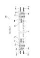
図1乃至図5は実施の形態1を示す図で、図1はLED照明システム100を示す図、図2はLED用点灯装置3の回路構成のブロック図、図3はLEDランプ7の概略構成を示す図、図4はLED照明システム100全体の概略回路図、図5は測定用抵抗13a,13bに対応して計算した測定用抵抗13a,13bの両端の電圧Viの計算結果を示す図である。 1 to 5 are diagrams showing the first embodiment, FIG. 1 is a diagram showing an
図1に示すように、LED照明システム100は、既存の直管蛍光ランプ用照明器具1にLED用点灯装置3を設置し、既存の安定器2(蛍光ランプ用点灯装置)に接続されている商用電源に接続される入力電線4と、安定器2からソケット5に接続される合計4本の出力電線6を外してLED用点灯装置3に接続し直し、既存のソケット5に、LEDランプ7(以下、単にランプと呼ぶ場合もある)を接続する。 As shown in FIG. 1, an
このとき、安定器2(蛍光ランプ用点灯装置)は、直管蛍光ランプ用照明器具1から取り外してもよいし、そのまま残しておいてもよい。 At this time, the ballast 2 (fluorescent lamp lighting device) may be removed from the direct fluorescent
LEDランプ7は、複数のLEDを備え、直管蛍光ランプの全長と、端部構造(口金、口金ピン等)、寸法などを合わせ、さらに全体を類似の形状にすることによって、両端の二つのソケット5に装着できるようにしたランプである。 The
LEDランプ7は、内部あるいは表面にLED16を並べて配置した細長い棒状の構体の両端に一対の金属製のピン(ピン12a−1とピン12a−2との組、ピン12b−1とピン12b−2との組(図3参照))を備えた口金7a,7bを備え、JIS C7617−2に規定された全長と、JIS C7709−1にG13もしくはG5として規定された口金寸法を持つ。 The
LEDランプ7は、直管蛍光ランプのようにフィラメントを使用しないので、本来はピン(口金ピン)は片側1本、計2本あればよいが、上記のように、直管蛍光ランプと類似の構成とするために、片側2本、計4本のピン(口金ピン)を備える。LEDランプ7の詳細は、後述する。 Since the
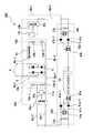
LED用点灯装置3は、図2に示すように、例えば、AC100Vである入力電線4が、先ず、整流回路8に接続され、直流に変換されて、図の両側の中間出力電線9a−1,9a−2,9b−1,9b−2に出力される。 As shown in FIG. 2, the
整流回路8は、例えば、図4に示すように全波整流するダイオードブリッジ31と、図示を省略しているが、平滑化回路で構成されて、直流を、出力電線6b−1,6a−1などに出力する。出力電線6b−1,6a−1は、ソケット5を介して、LEDランプ7へ電力を供給する。 The
接続判定用信号発生器10a,10bは、例えば、図4に示すように、接続判定用信号発生器10aは分圧抵抗10a−1,10a−2で構成されるとともに、接続判定用信号発生器10bは分圧抵抗10b−1,10b−2で構成される。接続判定用信号発生器10aは分圧した直流電圧を出力電線6a−1,6a−2の組へ出力し、接続判定用信号発生器10bは出力電線6b−1,6b−2の組へ出力するようになっている。 For example, as shown in FIG. 4, the connection
接続判定用信号発生器10a,10bは、ダイオードブリッジ31の正極(図4では上側)と負極(図4では下側)に並列に接続される。且つ、接続判定用信号発生器10aは、分圧抵抗10a−1がダイオードブリッジ31の正極側に、分圧抵抗10a−2がダイオードブリッジ31の負極側に接続される。また、接続判定用信号発生器10bは、分圧抵抗10b−2がダイオードブリッジ31の正極側に、分圧抵抗10b−1がダイオードブリッジ31の負極側に接続される。 The connection
一方、接続判定用信号発生器10aの分圧抵抗10a−2に並列に接続される電圧測定回路兼遮断信号発生回路11a(インピーダンス検知手段)は、出力電線6a−1,6a−2間の電圧を測定し、その電圧が所定の範囲(後述する)以外の場合には遮断信号を信号線34aを介して遮断回路35a(保護手段)に送り、遮断回路35aは、出力電線6a−1,6a−2への接続を遮断するようになっている。 On the other hand, the voltage measurement circuit / breaking
また、接続判定用信号発生器10bの分圧抵抗10b−2に並列に接続される電圧測定回路兼遮断信号発生回路11b(インピーダンス検知手段)は、出力電線6b−1,6b−2間の電圧を測定し、その電圧が所定の範囲(後述する)以外の場合には遮断信号を信号線34bを介して遮断回路35b(保護手段)に送り、遮断回路35bは、出力電線6b−1,6b−2への接続を遮断するようになっている。なお、この測定される電圧はLEDランプ7に設けられた測定用抵抗のインピーダンスで決まるので、間接的にインピーダンスを測定していることになる。 Further, the voltage measuring circuit / breaking
電圧測定回路兼遮断信号発生回路11a,11bの電圧測定回路部分は、この例では、50Hzより長い時間平均化した直流電圧を測定するようになっており、交流電圧の場合は0Vと測定される。さらに、一例では、ノイズ等の影響や、過渡的な変化の影響を避けるため、0.5秒程度の長い期間の平均をとるようにする。尚、この遮断回路35a,35bは、例えば、一度、遮断した後は、電源がオフになるまで保持され、次に電源がオンになるときにはリセットされ、通電状態になる。その他の例では、リセットスイッチを備え、リセットスイッチが押されるまで遮断状態としてもよい。このLED用点灯装置3においては、各ソケット5に出力される2本の出力電線6a−1,6a−2もしくは出力電線6b−1,6b−2のうち一方、図4の場合、出力電線6a−1と出力電線6b−1とにLEDを発光させる電力を出力する。 In this example, the voltage measurement circuit portions of the voltage measurement circuit / breaking
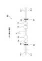
図3に示すように、LEDランプ7は、両端にそれぞれ一対(ピン12a−1,ピン12a−2の組、ピン12b−1,ピン12b−2の組)、すなわち合計4本のピン12a−1,12a−2,12b−1,12b−2を備え、照明器具側のソケット5に接続してLEDランプ7を支持できるようになっている。 As shown in FIG. 3, the
このピン12a−1,12a−2,12b−1,12b−2を含む管端部の寸法、ランプ全長等の直管蛍光ランプ用照明器具1に装着するための条件は、直管蛍光ランプを規定したJIS C7617−1もしくは2、さらには口金を規定したJIS C7709−1に記載されており、この条件を満たすようにしてある。 Conditions for mounting the
ピン12a−1とピン12a−2とは、インピーダンス、この例では、測定用抵抗13aの両端にそれぞれ接続される。ピン12b−1とピン12b−2も、同様に測定用抵抗13bの両端にそれぞれ接続されている。 The
さらに、測定用抵抗13a,13bは、それぞれ並列に、LED用点灯装置3の出力の検知手段14a,14b(点灯装置出力検知手段)に接続される。検知手段14a,14bは、例えば電圧計で、この場合、間接的にLED用点灯装置の出力あるいは出力特性を測定したことになり、所定のLED用点灯装置の出力に対応する所定の電圧範囲からはずれた場合には、電力を遮断する遮断信号を発生し、遮断信号線44a,44bにのせる。この場合、ピン12a−1と12a−2間と、ピン12b−1と12b−2間をそれぞれ端子間Aと呼ぶ。 Further, the measuring
入力選別回路41a,41bは、例えば、図4に示すように、入力選別回路41aはダイオード41a−1,41a−2、入力選別回路41bはダイオード41b−1,41b−2の2個ずつで構成される。 For example, as shown in FIG. 4, the
LED用点灯装置3から供給されたLEDを点灯させる電力がピン12a−1もしくはピン12a−2のいずれかに、あるいは、ピン12b−1もしくはピン12b−2のいずれかに出力されるが、いずれの場合でも適切にLEDに電力が供給される。 The power for lighting the LED supplied from the
例えば、図4の右側の端については、出力電線6b−1が、電力を供給する線になるが、分圧抵抗10b−1,10b−2によって、出力電線6b−1は出力電線6b−2より電圧が高くなっている。そのため、ダイオード41b−1の方がダイオード41b−2より電圧が高くなって、前者(ダイオード41b−1)が導通状態、後者(ダイオード41b−2)が遮断状態になるので、出力電線6b−1が遮断回路43bに接続されることになる。 For example, at the right end of FIG. 4, the
一方、ダイオード41b−2によって、出力電線6b−1とは遮断状態になるため、検知手段14bへの出力電線6b−2からの接続には影響を与えない。 On the other hand, since the
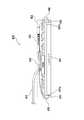
図4のLED照明システム100における電流の流れる経路は、ダイオードブリッジ31の正極(図4では上側)から遮断回路35b、出力電線6b−1、ダイオード41b−1、遮断回路43b、電流制御回路15、複数の発光ダイオード16、遮断回路43a、ダイオード41a−2、検知手段14a、出力電線6a−1、遮断回路35a、ダイオードブリッジ31の負極(図4では下側)への流れとなる。 In the
図4のLED照明システム100において、LEDランプ7の前後方向(図4では上下方向)を、図4と逆方向に取り付けてもよい。その場合の電流の流れる経路は、ダイオードブリッジ31の正極(図4では上側)から遮断回路35b、出力電線6b−1、ダイオード41b−2、遮断回路43b、電流制御回路15、複数の発光ダイオード16、遮断回路43a、ダイオード41a−1、検知手段14a、出力電線6a−1、遮断回路35a、ダイオードブリッジ31の負極(図4では下側)への流れとなる。 In the
図4のLED照明システム100において、LEDランプ7の左右方向は一方向に限定される。図4とLEDランプ7の左右方向を逆に取り付けた場合は、図4のLED用点灯装置3は、電位が左側よりも右側が高くなる構成であるから、LEDランプ7には電流が流れないため、LEDランプ7は点灯しない。 In the
尚、この例では、検知手段14a,14bは、50Hzより長い時間平均化した直流電圧を測定するようになっており、交流電圧の場合は0Vと測定される。さらに、一例では、ノイズ等の影響や、過渡的な変化の影響を避けるため、0.5秒程度の長い期間の平均をとるようにする。 In this example, the detection means 14a and 14b measure a DC voltage averaged for a time longer than 50 Hz. In the case of an AC voltage, the detection means 14a and 14b measures 0V. Furthermore, in one example, in order to avoid the influence of noise or the like or the influence of a transient change, an average of a long period of about 0.5 seconds is taken.
遮断回路43a,43b(保護手段)は、検知手段14a,14bからの遮断信号が遮断信号線44a,44bを介して送られてきた場合、出力電線6a−1,6b−1から送られてきた電力を遮断する。電流制御回路15、複数の発光ダイオード16は直列に接続され、適当な電流に制御されて、発光ダイオード16は適切な発光をする。電流制御回路15は一例では抵抗であるが、発光出力をより安定化させるため、定電流回路としてもよい。 The
なお、遮断回路43a,43bは、例えば、一度、遮断した後は、電源がオフになるまで保持され、次に電源がオンになるときにはリセットされ、通電状態になるようにしているが、他の例では、リセットスイッチを備え、リセットスイッチが押されるまで遮断状態としてもよい。 The
ランプ全長1198mmに対応した照明器具で、JIS C7617−2で規定されたFLR40S、FL40S、FL40SS/37、FHF32等を装着可能となっているLED照明器具について具体的に一例を説明する。 A specific example of an LED lighting fixture that can be mounted with FLR40S, FL40S, FL40SS / 37, FHF32, etc., as defined in JIS C7617-2, is a lighting fixture corresponding to a lamp total length of 1198 mm.
LED用点灯装置3は、合計4本ある出力電線6a−1,6a−2,6b−1,6b−2のうちの少なくとも一組、例えば、図2あるいは図4の例では、同じ端にあるソケット5に接続された1対の出力電線6a−1と出力電線6a−2との組と、出力電線6b−1と出力電線6b−2との組に、接続判定用信号発生器10a,10bから接続判定用信号を出力する。接続判定用信号発生器10aから、出力電線6a−1と出力電線6a−2との組に接続判定用信号を出力する。また、接続判定用信号発生器10bから、出力電線6b−1と出力電線6b−2との組に接続判定用信号を出力する。 The
接続判定用信号発生器10aは、例えば、分圧抵抗10a−1,10a−2で作られた出力インピーダンスが有限の電圧を発生する回路である。なお、出力インピーダンスが有限という意味は、出力側に接続される回路のインピーダンスにより発生電圧が変化するという意味である。 The connection
また、接続判定用信号発生器10bは、例えば、分圧抵抗10b−1,10b−2で作られた出力インピーダンスが有限の電圧を発生する回路である。 The connection
例えば、電源がAC100Vで、分圧抵抗10a−1,10a−2,10b−1,10b−2を、それぞれ、90kΩ、15kΩ、90kΩ、15kΩ(それぞれRd11,Rd12,Rd21,Rd22とする)とする。即ち、
Rd11(分圧抵抗10a−1)=90kΩ
Rd12(分圧抵抗10a−2)=15kΩ
Rd21(分圧抵抗10b−1)=90kΩ
Rd22(分圧抵抗10b−2)=15kΩ
である。For example, the power source is AC100V, and the
Rd11 (
Rd12 (
Rd21 (
Rd22 (
It is.
また、正常なLEDランプ7の測定用抵抗13a,13bを15kΩ±3kΩ(それぞれRm1,Rm2とする)とする。即ち、
Rm1(測定用抵抗13a)=15kΩ±3kΩ
Rm2(測定用抵抗13b)=15kΩ±3kΩFurther, the
Rm1 (
Rm2 (
LED用点灯装置3の電圧測定回路兼遮断信号発生回路11a,11bとLEDランプ7の検知手段14a,14bが遮断信号を発生させない電圧範囲を6.0Vから12.0Vの間とした。 The voltage range in which the voltage measurement circuit / breaking
さらに、整流回路8によって出力される電圧V0は、ダイオード4個による全波整流回路部分と単純なコンデンサによる平滑回路とした場合、負荷により100Vから141Vに変化する。この場合、測定用抵抗13a,13bの両端の電圧V1,V2は、以下のようになる。
Vi = V0×[1/(1/Rmi+1/Rdi2)]/[Rdi1+{1/(1/Rmi+1/Rdi2)}]
但し、iは、1または2であり、それぞれ、左側と右側の回路に対応している。測定用抵抗13a,13bの上限値、中心値、下限値(18k,15k,12k)に対応して計算した例を図5に示す。Further, the voltage V0 output from the
Vi = V0 × [1 / (1 /
However, i is 1 or 2, and corresponds to the left and right circuits, respectively. FIG. 5 shows an example calculated corresponding to the upper limit value, the center value, and the lower limit values (18k, 15k, 12k) of the
図5に示すように、No1からNo6は、測定用抵抗13a,13bが上記3通り(18k,15k,12k)の場合と、整流回路8によって出力される電圧V0の上下限値である141Vと100Vの2通りの組み合わせ、計6通りについて計算した結果で、電圧Viが6.90Vから11.75V範囲内になることがわかる。このため、LED用点灯装置3とLEDランプ7の遮断しない範囲である6.0Vから12.0Vの範囲に入っており、いずれも遮断信号は発生されずそれぞれの遮断回路35a,35bと遮断回路43a,4bは回路を遮断せず、結局、LED16に電力が供給され、発光することになる。 As shown in FIG. 5, in No. 1 to No. 6, when the
この実施の形態1によるLED用点灯装置3を装着した直管蛍光ランプ用照明器具1に、誤って、直管蛍光ランプを装着した場合について説明する。直管蛍光ランプの一方の端の抵抗(二つの口金ピンの間の抵抗、即ちフィラメントの抵抗)は正常な状態で、室温で1.5Ωから4Ω程度、最大でも100Ω以下で、通電して温度が上がった状態で、その5倍程度であり、総合すると1.5Ωから500Ωということになる。 A case will be described in which a straight tube fluorescent lamp is mistakenly attached to the straight tube fluorescent
一方、異常な状態としては、寿命末期などでフィラメントが断線した場合、∞Ωあるいは500kΩ以上、また、寿命末期を含めた短絡するような異常時0Ωあるいは、0.5Ω以下という場合がある。従って、正常時と異常時を含めて、とりうる抵抗は0Ωから500Ωの範囲と、500kΩ以上となる。 On the other hand, the abnormal state may be ∞Ω or 500 kΩ or more when the filament is broken at the end of the life, or 0Ω or 0.5Ω or less at the time of an abnormality including a short circuit including the end of the life. Therefore, the resistance that can be taken including normal and abnormal conditions is in the range of 0Ω to 500Ω and 500 kΩ or more.
図5のNo7からNo12は、Rdi1=90kΩ、Rdi2=15kΩ、整流回路8によって出力される電圧V0=100Vのとき、測定用抵抗Rmiを1Ω、20Ω、100Ω、500Ω、100kΩ、1000kΩと変化させたときの測定用抵抗13a,13bの両端の電圧Vi(iは1または2)を計算した結果である。 In No. 7 to No. 12 in FIG. 5, when Rdi1 = 90 kΩ, Rdi2 = 15 kΩ, and the voltage V0 = 100 V output from the
上述したように、直管蛍光ランプの正常時と異常時を含めて、とりうる抵抗は0Ωから500Ωの範囲と、500kΩ以上であるが、その時の測定用抵抗13aもしくは測定用抵抗13bの両端の電圧V1もしくはV2は、
(1)0Ωから500Ωの範囲のとき(正常時):0.53V以下(図5のNo7〜No10より)。
(2)500kΩ以上のとき(異常時):12.66V以上(図5のNo11、No12より)。
となる。As described above, the resistance that can be taken including normal and abnormal conditions of the straight tube fluorescent lamp is in the range of 0Ω to 500Ω and 500 kΩ or more, but at both ends of the
(1) When in the range of 0Ω to 500Ω (normal): 0.53 V or less (from No7 to No10 in FIG. 5).
(2) When 500 kΩ or more (at the time of abnormality): 12.66 V or more (from No11 and No12 in FIG. 5).
It becomes.
上記(1)、(2)の範囲は、LED用点灯装置3の電圧測定回路兼遮断信号発生回路11a,11bが遮断信号を発生させない電圧範囲である6.0V〜12.0Vから外れているため、LED用点灯装置3の電圧測定回路兼遮断信号発生回路11a,11bが遮断信号を発生し、遮断回路35a,35bが回路を遮断し、直管蛍光ランプへの出力は遮断される。 The above ranges (1) and (2) are out of the voltage range of 6.0 V to 12.0 V, in which the voltage measuring circuit / breaking
このように、誤って、LED用点灯装置3を装着した直管蛍光ランプ用照明器具1に直管蛍光ランプを装着した場合は、LED用点灯装置3の遮断回路35a,35が出力回路を遮断するため、発熱や発煙の事故は起こらない。 As described above, when the straight tube fluorescent lamp is mounted on the
図5におけるNo13〜No16は、LED用点灯装置3の電圧測定回路兼遮断信号発生回路11a,11bが遮断信号を発生させない電圧範囲である6.0V〜12.0Vの下限値(6.0V)と上限値(12.0V)になる測定用抵抗Rmiを計算で求めた結果である。Rdi1=90kΩ、Rdi2=15kΩ、整流回路8によって出力される電圧V0=100V、141Vについて計算している。電圧V0=100Vのとき、電圧Vi=6.0Vになる測定用抵抗Rmiは9.3kΩ、電圧Vi=12.0Vになる測定用抵抗Rmiは67.5kΩである。また、電圧V0=141Vのとき、電圧Vi=6.0Vになる測定用抵抗Rmiは5.45kΩ、電圧Vi=12.0Vになる測定用抵抗Rmiは18.95kΩである。 No. 13 to No. 16 in FIG. 5 are lower limit values (6.0 V) of 6.0 V to 12.0 V, which is a voltage range in which the voltage measuring circuit / cut-off
尚、正常状態から異常状態に変化する過程で、500Ωから500kΩの範囲を短期間とる場合があるが、短時間の間に500Ω以下か、100kΩ以上に変化するので、短時間に遮断される。従って、直管蛍光ランプのとりうる抵抗として、500Ωから500kΩの範囲は除外してよい。 In the process of changing from the normal state to the abnormal state, the range from 500Ω to 500kΩ may be taken for a short period of time, but since it changes to 500Ω or less or 100kΩ or more in a short time, it is cut off in a short time. Therefore, the range of 500Ω to 500kΩ may be excluded as the resistance that the straight tube fluorescent lamp can take.
また、実際は、この例では、Rdi1が90kΩの場合、直管蛍光ランプのフィラメントには、100[V]/90,000[Ω]=0.001[A]程度(高めにみても)の電流しか流れないため、ほとんど、直管蛍光ランプのフィラメントの温度は上がらず、直管蛍光ランプとして可能性のある抵抗範囲はさらに狭くなる。従って、下限値を50Ωから100Ωとしても現実的には問題は起こらない可能性が強く、一方、上限値も直管蛍光ランプのフィラメントが切れた場合は、数MΩ以上の抵抗があり、1MΩ程度までは問題が起こらない可能性が強い。 Actually, in this example, when Rdi1 is 90 kΩ, the filament of the straight tube fluorescent lamp has a current of about 100 [V] / 90,000 [Ω] = 0.001 [A] (even if high). However, since the temperature of the filament of the straight tube fluorescent lamp does not rise, the resistance range that can be used as a straight tube fluorescent lamp is further narrowed. Therefore, even if the lower limit is set to 50Ω to 100Ω, there is a strong possibility that no problem actually occurs. On the other hand, when the filament of the straight tube fluorescent lamp is broken, there is a resistance of several MΩ or more and about 1MΩ. Until then, there is a strong possibility that problems will not occur.
即ち、測定用抵抗13a,13b(Rm1,Rm2)の最も適当な抵抗値範囲は、上述したように直管蛍光ランプの正常時と異常時を含めて、とりうる抵抗は0Ωから500Ωの範囲と、500kΩ以上であるので(正常状態から異常状態に変化する過程で、500Ωから500kΩの範囲を短期間とる場合があるが、短時間の間に500Ω以下か、100kΩ以上に変化し短時間に遮断されるので除外する)、それらとは異なる500Ωから500kΩの間ということになるが、50Ω〜1MΩ程度でも可能である。 That is, the most appropriate resistance value range of the
この実施の形態1によるLEDランプ7を、改造していない直管蛍光ランプ用照明器具1に誤って装着した場合について説明する。直管蛍光ランプ用照明器具1の各ソケット5への1対の端子への出力は、グロー管形、ラピッド形、インバータ形いずれも、商用周波数あるいは、高周波の交流で、一方、このLEDランプ7の検知手段14a,14bは、上記のように、直流成分の電圧のみ有限な値を検知し、交流の場合は0Vと検知する。 A case will be described in which the
検知手段14a,14bが遮断信号を発生させない電圧範囲を6.0Vから12.0Vの間としたので、検知手段14a,14bは遮断信号を発生し、遮断回路43a,43bに送られるため、電力を遮断する。遮断回路43a,43bで、検知手段14a,14bからの遮断信号が遮断信号線44a,44bを介して遮断回路43a,43bに送られ、遮断回路43a,43bは、出力電線6a−1,6b−1から送られてきた電力を遮断する。 Since the voltage range in which the detection means 14a, 14b does not generate the cutoff signal is between 6.0V and 12.0V, the detection means 14a, 14b generates a cutoff signal and is sent to the
このように、誤って、改造していない直管蛍光ランプ用照明器具1にLEDランプ7を装着した場合は、LEDランプ7が回路を遮断し、電圧・電流を遮断されるため、発熱や発煙の事故は起こらない。 As described above, when the
LED用点灯装置3を電源に接続した直後は、出力電線6a−1,6b−1間、さらに、LEDランプ7のLEDまで電力を供給できる通電状態にしておいて電圧等をチェックし、判定して範囲外の場合、遮断するようにしてもよいし、電源に接続した直後は、LED用点灯装置3側、LEDランプ7側とも遮断状態にしておいて、電圧等をチェックし、範囲内であると判定した後、通電状態にしてもよい。後者は、スイッチオン後発光するまでに、若干時間がかかるが、より安全である。具体的な動作としては、まず、LEDランプ7側の両方の遮断回路43a,43bを遮断状態とし、LED用点灯装置3側の遮断回路35a,35bのうち一方、例えば遮断回路35aを導通状態とし、判定した後、もう一方の遮断回路35bを導通状態にして、さらに、LEDランプ7側で、チェックするように構成する。LED用点灯装置3側の遮断回路35a,35bをはじめに一方のみ開く理由は、チェックするためには、遮断回路35a,35bを導通状態にしなくてはならないが、両方同時に導通状態にした場合、誤って所定のLEDランプ7以外のランプを装着したときに、一時的に電流が流れ、その時点で問題が起こることを避けるためである。 Immediately after the
この実施の形態1について説明した例では、LED用点灯装置3側、LEDランプ7側とも両方の端に検知電圧測定回路兼遮断信号発生回路11a,11b、接続判定用信号発生器10a,10b、あるいは検知手段14a,14b、測定用抵抗13a,13bを設けたが、どちらも一方の端のみに設けてもよく効果があるが、両方に設けた方がより安全である。 In the example described in the first embodiment, both the
この実施の形態1について説明した例では、接続判定用信号発生器10a,10bの出力は、幅のある電圧を抵抗で分圧した信号を用いていたが、例えば、定電流源などでもよく、その場合、より精度よく、検知が可能になる。また、特定の周波数の信号としたりしてもよく、これに対応して、LEDランプ側のインピーダンスを設定する素子を抵抗ではなく、コンデンサにするなどでもよい。 In the example described in the first embodiment, the output of the connection
実施の形態2.
図6乃至図9は実施の形態2を示す図で、図6はLED照明システム200を示す図、図7はLED用点灯装置203の回路構成のブロック図、図8はLEDランプ207の概略構成を示す図、図9はLED照明システム200全体の概略回路図である。
6 to 9 are diagrams showing the second embodiment, FIG. 6 is a diagram showing the
図6に示すように、LED照明システム200は、LED照明システム100と同様、既存の直管蛍光ランプ用照明器具1にLED用点灯装置203を設置し、既存の安定器2(蛍光ランプ用点灯装置)に接続されている商用電源に接続される入力電線4と、安定器2からソケット5に接続される合計4本の出力電線6を外してLED用点灯装置203に接続し直し、既存のソケット5に、LEDランプ207(以下、単にランプと呼ぶ場合もある)を接続する。 As shown in FIG. 6, the
LED照明システム200は、LED用点灯装置203とLEDランプ207とが、LED照明システム100と異なる。 The
図7に示すように、LED用点灯装置203は、整流回路8、接続判定用信号発生器10a,10b、電圧測定回路兼遮断信号発生回路11a,11b、遮断回路35a,35bに加えて、電流制御回路15を備えている。 As shown in FIG. 7, the
LED用点灯装置203は、図7に示すように、例えば、AC100Vである入力電線4が、先ず、整流回路8に接続され、直流に変換されて、図の両側の中間出力電線9a−1,9a−2,9b−1,9b−2に出力される。 As shown in FIG. 7, in the
電流制御回路15は、電気的には、整流回路8と、接続判定用信号発生器10bとの間に接続され、定電流回路あるいは、電流制限抵抗で、LED16に流れる電流、すなわち、電力をコントロールする。 The
図8に示すように、LEDランプ207側には、電流制御回路15はなく、LED16と、安全用の回路、すなわち、測定用抵抗13a,13b、検知手段14a,14b、入力選別回路41a,41b、遮断回路43a,43bを備える。 As shown in FIG. 8, there is no
図9に示すように、LED照明システム200は、LED用点灯装置203と、LEDランプ207とで構成される。LED用点灯装置203の整流回路8、接続判定用信号発生器10a,10b、LED用点灯装置203の入力選別回路41a,41bの構成は、図4のLED照明システム100のものと同じである。 As shown in FIG. 9, the
LED16の点灯に関する動作は、実施の形態1では、LEDランプ7側にあった電流制御回路15をLED用点灯装置203側に設けただけで、同様である。電流制御回路15を定電流回路とした一例では、点灯時の電流、例えば、20Wとした設計では、0.2A(0.2x100=20W)あるいは40Wと設計では、0.4A(0.4x100=40W)になるまでは、導通状態となるように設計される。電流制御回路15を抵抗とした例では、抵抗分の電圧降下を10V(100Vの10%)と設計すると、20W、40Wそれぞれ、50Ω、25Ωとなる。 The operation related to lighting of the
電源をオンにした直後は、遮断回路35a,35b,43a,43bが遮断状態で、一つでも遮断状態の間は、出力電線6a−1,6b−1、LED16等で構成されるメインの電流は流れない。この状態では、分圧抵抗10a−1,10a−2,10b−1,10b−2と、測定用抵抗13a,13bの抵抗値を、図5で示す値にした場合、上記の制御回路を定電流回路とした例では、流れる電流が0.001A(<100V/Rdi1 =100/90,000≒0.001)程度なので、電流制御回路15の定電流回路は導通となり、電流制御回路15を上記の抵抗とした例では、Rdi1等と比較すると抵抗が非常に小さく、いずれも、電流制御回路15が入らない状態とほとんど変わらない。 Immediately after the power is turned on, the
一方、点灯中、すなわち、4個の遮断回路35a,35b、43a,43bの全てが導通状態の場合は、上記の例では、いずれの方式でも電流制御回路15の電圧降下分は電源電圧の10%程度なので、図9の右側の回路について分圧抵抗10b−1,10b−2にかかる電圧が10%小さくなり、測定用抵抗13bに流れる電流は10%減少する。このため、LEDランプ207側の検知手段14bと、LED用点灯装置203側の電圧測定回路兼遮断信号発生回路11bで検知される電圧は、10%小さくなる。このため、一例では、遮断判定電圧の下限値を10%下げればよい。一方、図9の左側の回路は、実施の形態1と同じである。いずれの側も実施の形態1と同様に動作する。 On the other hand, during lighting, that is, when all of the four
実施の形態3.
図10乃至図13は実施の形態3を示す図で、図10はLED照明システム300を示す図、図11はLED用点灯装置303の回路構成のブロック図、図12はLEDランプ307の概略構成を示す図、図13はLED照明システム300全体の概略回路図である。
FIGS. 10 to 13 are
図10に示すように、LED照明システム300は、LED照明システム100と同様、既存の直管蛍光ランプ用照明器具1にLED用点灯装置303を設置し、既存の安定器2(蛍光ランプ用点灯装置)に接続されている商用電源に接続される入力電線4と、安定器2からソケット5に接続される合計4本の出力電線6を外してLED用点灯装置303に接続し直し、既存のソケット5に、LEDランプ307(以下、単にランプと呼ぶ場合もある)を接続する。 As shown in FIG. 10, the
LED照明システム300は、LED用点灯装置303とLEDランプ307とが、LED照明システム100と異なる。 The
図11に示すように、LED用点灯装置303は接続判定用信号発生器10a,10b、電圧測定回路兼遮断信号発生回路11a,11b、遮断回路35a,35bで構成される。 As shown in FIG. 11, the
図12に示すように、整流回路8、電流制御回路15は、LEDランプ307に設けられている。従って、LED用点灯装置303の出力電線6a−1,6a−2,6b−1,6b−2は、交流のままで、特に、出力電線6a−1、6b−1はAC100Vの商用電圧が、そのまま接続されることになる。 As shown in FIG. 12, the
図13に示すように、出力電線6a−1,6a−2,6b−1,6b−2はソケット5を介して、LEDランプ7の口金に接続される。さらに、測定用抵抗13a,13b、高周波導通用コンデンサ45a,45b、検知手段14a,14bが並列につながれ、入力選別回路41a,41b、遮断回路43a,43bを介して、整流回路8に接続される。整流回路8に入力される電圧はAC100Vのままであるが、ここで、整流され、場合によってはさらに平滑されて電流制御回路15とLED16の直列回路に出力され、制御された直流電流によって、LED16が発光する。 As shown in FIG. 13, the output
実施の形態1と同様、接続判定用信号発生器10a,10bは、一例では、分圧抵抗10a−1,10a−2、10b−1,10b−2で構成されるが、入力がAC100Vなので、交流が出力される。遮断回路35a,35bが導通状態の場合は、出力電線6a−1,6a−2,6b−1,6b−2を介して、測定用抵抗13a,13bに接続され、結局、入力された交流電圧に対して、両端(図13の左右)で独立に、図13の左側は、分圧抵抗10a−1,10a−2、測定用抵抗13a、高周波導通用コンデンサ45a、右側は、分圧抵抗10b−1,10b−2、測定用抵抗13b、高周波導通用コンデンサ45bで、それぞれ3個の抵抗と1個のコンデンサで決まる電圧を電圧測定回路兼遮断信号発生回路11a,11bと検知手段14a,14bの測定位置に生じさせる。電圧測定回路兼遮断信号発生回路11a,11bと検知手段14a,14bは、この例では、交流電圧計である。 As in the first embodiment, the connection
この分圧抵抗10a−1,10a−2,10b−1,10b−2と測定用抵抗13a,13bに、実施の形態1の抵抗をそのまま使い、さらに高周波導通用コンデンサ45a,45bを商用周波数では、ほとんど、導通しない容量にした場合は、直流電圧を、交流電圧の実効値に置き換えたことになり、同様な値で測定される。 The
このため、LED用点灯装置303に、誤って、直管蛍光ランプが装着された場合は、実施の形態1と同様に作用して、遮断回路35a,35bが回路を遮断し、直管蛍光ランプにおいて加熱、発煙などの事故が起こることがない。なお、後述するように、高周波導通用コンデンサ45a,45bは10%程度、電圧を低下させる可能性があり、無視できる場合もあるが、もし、無視できない場合は、高周波導通用コンデンサ45a,45bの容量に合わせて、遮断信号が発生しない範囲6.0V〜12.0Vの特に下限値を10%程度下げればよい(5.4V〜12.0V)。 For this reason, when a straight tube fluorescent lamp is mistakenly attached to the
一方、安定器2(蛍光ランプ用点灯装置)からLED用点灯装置303に取り替えていないもともとの直管蛍光ランプ用照明器具1に、誤って、このLEDランプ307を装着した場合は、検知手段14a,14bが、直管蛍光ランプのフィラメントへ印加する電圧をそのまま検知する。 On the other hand, when the
以下、一例として、管長が1198mmのタイプで説明する。安定器2(蛍光ランプ用点灯装置)がグロー管タイプの場合、ランプの両端の端子には、約200Vが印加され、グロー管の放電と、両端の測定用抵抗13a,13bが直列になる。このグロー管の放電電圧は、150V程度で、測定用抵抗13a,13bの両端の電圧はそれぞれ25V程度になる。遮断信号は実施の形態1と同様6.0Vから12.0Vで発生させないとしているので、遮断される。 Hereinafter, as an example, a pipe length of 1198 mm will be described. When the ballast 2 (fluorescent lamp lighting device) is a glow tube type, approximately 200 V is applied to the terminals at both ends of the lamp, and the discharge of the glow tube and measuring
また、蛍光ランプ用点灯装置がラピッドスタートタイプは、フィラメント用トランスがフィラメントを加熱するための電圧を独立に発生させ、フィラメントに印加するようになっているが、JIS C7617−2で、3.4Vから4.2Vと決められており、従って、遮断信号が発生しない範囲6.0Vから12.0Vからはずれているため、遮断される。 In addition, when the fluorescent lamp lighting device is a rapid start type, the filament transformer independently generates a voltage for heating the filament and applies it to the filament, but it is 3.4 V according to JIS C7617-2. Therefore, the voltage is cut off because it is out of the range of 6.0 V to 12.0 V where no cutoff signal is generated.
また、蛍光ランプ用点灯装置がインバータタイプの場合、フィラメントでないものに接続されることなどから発生する電圧の幅が広く、高周波導通用コンデンサ45a,45bを設けない場合には、遮断信号が発生しない範囲6.0Vから12.0Vにはいる可能性がある。 In addition, when the fluorescent lamp lighting device is an inverter type, a voltage generated due to being connected to a non-filament is wide, and when the high-
この高周波導通用コンデンサ45a,45bは、10kHz以上の高周波の回路に接続された場合に、検知手段14a,14bの電圧を低下させるために設けてあり、一例では、例えば、0.02μFとする。その場合、60Hzでは133kΩ相当、通常のインバータの最低の周波数である20kHzの場合、400Ω相当と計算される(抵抗=1/2πfC、ここで、f:周波数、C:容量)。 The high-
並列の測定用抵抗13a,13bは、一例として、15kΩとしており、60Hzでは、コンデンサ分で10%程度の偏差になり、両端の電圧が10%程度低下する。一方、インバータすなわち20kHz以上の場合は、ほとんど、コンデンサを通って電流が流れるため、両端の電圧は3%以下(<400Ω/15000Ω)になり、もし、フィラメントに20V印加する設計でも0.6V程度(20×3%=0.6V)になり、遮断信号が発生しない範囲6.0Vから12.0V以下となって回路を遮断する。 The
この実施の形態1〜3に係るLED照明システムは、既存の直管蛍光ランプ用照明器具に、LED用点灯装置を設置し、既存の蛍光ランプ用点灯装置に接続されている商用電源に接続される入力電線と、既存のソケットに接続される出力電線をはずしてLED用点灯装置に接続し直し、ソケットにLEDランプを接続するLED照明システムであって、
LEDランプの両端のいずれかの端子間を端子間Aとし、端子間Aに接続されるLED用点灯装置からの出力の特性を既存の蛍光ランプ用点灯装置と異なるものとし、LEDランプにLED用点灯装置からの出力を検知する点灯装置出力検知手段を備えるとともに、点灯装置出力検知手段で検知した出力が、予め決められた範囲外の場合に、LEDランプへの入力を遮断する保護手段をLEDランプに備えたものである。In the LED lighting systems according to the first to third embodiments, an LED lighting device is installed in an existing lighting device for a straight tube fluorescent lamp, and is connected to a commercial power source connected to the existing fluorescent lamp lighting device. An LED lighting system in which an input wire and an output wire connected to an existing socket are removed and reconnected to an LED lighting device, and an LED lamp is connected to the socket,
The terminal between the terminals at both ends of the LED lamp is defined as A between terminals, and the output characteristics from the LED lighting device connected between the terminals A are different from those of the existing fluorescent lamp lighting device. In addition to the lighting device output detection means for detecting the output from the lighting device, when the output detected by the lighting device output detection means is out of a predetermined range, the protection means for blocking the input to the LED lamp It is for the lamp.
この実施の形態1〜3に係るLED照明システムは、LEDランプの端子間Aのインピーダンスを、蛍光ランプの通常状態と寿命末期状態とのいずれとも異なるインピーダンスとし、かつ、端子間Aに対応したLED用点灯装置側に、端子間Aのインピーダンスを直接または間接的に検知するインピーダンス検知手段を備えるとともに、さらに、インピーダンス検知手段が検知した端子間Aのインピーダンスが、予め決められた範囲外のインピーダンスの場合に、LED用点灯装置の出力を遮断する保護手段をLED用点灯装置に備えたものである。 In the LED lighting systems according to the first to third embodiments, the impedance between the terminals A of the LED lamps is different from both the normal state and the end-of-life state of the fluorescent lamp, and the LEDs corresponding to the terminals A The lighting device side includes an impedance detection means for directly or indirectly detecting the impedance between the terminals A, and the impedance between the terminals A detected by the impedance detection means is an impedance outside the predetermined range. In this case, the LED lighting device is provided with a protection means for blocking the output of the LED lighting device.
この実施の形態1〜3に係るLEDランプは、内部あるいは表面にLEDを並べて配置した細長い棒状の構体の両端に一対の金属製のピンを備えた口金を備え、JIS C7617−2に規定された全長と、JIS C7709−1にG13もしくはG5として規定された口金寸法を持つLEDランプであって、
両端のいずれかの端子間を端子間Aとし、前記端子間Aのインピーダンスを、蛍光ランプの通常状態と寿命末期状態のいずれとも異なるインピーダンスとし、かつ、LED用点灯装置からの出力を検知する点灯装置出力検知手段を備えるとともに、点灯装置出力検知手段で検知した出力が、予め決められた範囲外の場合に、当該LEDランプへの入力を遮断する保護手段を備えたものである。The LED lamps according to the first to third embodiments are provided with a base having a pair of metal pins at both ends of an elongated rod-like structure in which LEDs are arranged inside or on the surface, and are defined in JIS C7617-2. An LED lamp having a full length and a cap size defined as G13 or G5 in JIS C7709-1,
The terminal between the terminals at both ends is the terminal A, and the impedance of the terminal A is different from the normal state and the end-of-life state of the fluorescent lamp, and the output for detecting the output from the LED lighting device is detected. The apparatus includes a device output detection unit, and a protection unit that blocks input to the LED lamp when the output detected by the lighting device output detection unit is outside a predetermined range.
この実施の形態1〜3に係るLEDランプは、少なくとも一方の端の口金の2本のピン間に500Ωから500kΩの抵抗を設けたものである。 In the LED lamps according to the first to third embodiments, a resistance of 500Ω to 500 kΩ is provided between two pins of the base at one end.
この実施の形態1〜3に係るLEDランプは、LED用点灯装置からの直流電圧あるいは電流で動作し、かつ、入力端子間の印加電圧が交流か直流かを検知する検知手段を備え、交流の場合、遮断する保護手段を備えたものである。 The LED lamps according to the first to third embodiments are operated with a DC voltage or current from the LED lighting device, and include a detection unit that detects whether the applied voltage between the input terminals is AC or DC. In this case, a protective means for blocking is provided.
この実施の形態1〜3に係るLEDランプは、抵抗に接続された端子間Aの印加電圧の検知手段を備え、LED用点灯装置によって流される電流と抵抗の前記範囲の抵抗値から計算される電圧をはずれている場合、遮断する保護手段を備えたものである。 The LED lamps according to the first to third embodiments are provided with a means for detecting an applied voltage between terminals A connected to a resistor, and are calculated from the current flowed by the LED lighting device and the resistance value in the above-described range. A protective means is provided to cut off when the voltage is off.
この実施の形態1〜3に係るLED用点灯装置は、LEDランプの口金へ接続される出力端子を備え、出力端子からの少なくとも一部の出力を蛍光ランプ点灯装置の出力と異なるものとし、さらに出力端子に、LEDランプ端子間のインピーダンスを測定するインピーダンス検知手段を備え、インピーダンス検知手段が検知したLEDランプ端子間のインピーダンスが、所定の範囲外の場合に出力を遮断する保護手段を備えたものである。 The LED lighting device according to the first to third embodiments includes an output terminal connected to the base of the LED lamp, and at least a part of the output from the output terminal is different from the output of the fluorescent lamp lighting device. Impedance detecting means for measuring the impedance between the LED lamp terminals at the output terminal, and protective means for cutting off the output when the impedance between the LED lamp terminals detected by the impedance detecting means is outside a predetermined range It is.
この実施の形態1〜3に係るLED用点灯装置は、少なくとも一方のソケットへ接続される一対の端子間に、一定電流、あるいは負荷によって電圧の変化する出力を、少なくとも始動時に出力し、かつ、端子間の電圧の検知手段を備え、検知手段が検知する端子間の電圧が所定範囲外の場合に、出力を遮断する保護手段を備えたものである。 The LED lighting device according to the first to third embodiments outputs a constant current or an output whose voltage changes depending on a load between a pair of terminals connected to at least one socket, at least at the time of starting, and A voltage detecting means between terminals is provided, and a protective means for cutting off the output when the voltage between the terminals detected by the detecting means is outside a predetermined range is provided.
この実施の形態1〜3に係るLED照明システムは、LEDランプの両端のいずれかの端子間を端子間Aとし、端子間Aに接続されるLED用点灯装置からの出力の特性を既存の蛍光ランプ用点灯装置と異なるものとし、LEDランプにLED用点灯装置からの出力を検知する点灯装置出力検知手段を備えるとともに、点灯装置出力検知手段で検知した出力が、予め決められた範囲外の場合に、LEDランプへの入力を遮断する保護手段をLEDランプに備えた構成にしたので、通常の蛍光ランプ用照明器具に、誤って、このLEDランプを装着した場合には、端子間Aへの出力を検知し、さらに保護手段によって入力を遮断することにより、発熱や発煙が起こらないようにできる。 In the LED lighting systems according to the first to third embodiments, the terminal between the terminals at both ends of the LED lamp is defined as the inter-terminal A, and the output characteristics from the LED lighting device connected to the inter-terminal A are represented by the existing fluorescence. When the LED lamp is provided with a lighting device output detection means for detecting the output from the LED lighting device, and the output detected by the lighting device output detection means is outside a predetermined range. In addition, since the LED lamp is provided with a protective means for blocking the input to the LED lamp, if this LED lamp is mistakenly attached to a normal fluorescent lamp lighting fixture, By detecting the output and further blocking the input by a protective means, it is possible to prevent heat generation and smoke generation.
この実施の形態1〜3に係るLED照明システムは、LEDランプの端子間Aのインピーダンスを、蛍光ランプの通常状態と寿命末期状態とのいずれとも異なるインピーダンスとし、かつ、端子間Aに対応したLED用点灯装置側に、端子間Aのインピーダンスを直接または間接的に検知するインピーダンス検知手段を備えるとともに、さらに、インピーダンス検知手段が検知した端子間Aのインピーダンスが、予め決められた範囲外のインピーダンスの場合に、LED用点灯装置の出力を遮断する保護手段をLED用点灯装置に備えた構成にしたので、このLED用点灯装置付きの照明器具に蛍光ランプを誤って装着した場合に、LED用点灯装置は、端子間Aのインピーダンスを検知し、その検知したインピーダンスがLEDランプの端子間Aに設定されているインピーダンスの範囲外となるため、保護手段によって、ランプ側への出力を遮断することにより、発熱や発煙等が起こらないようにできる。 In the LED lighting systems according to the first to third embodiments, the impedance between the terminals A of the LED lamps is different from both the normal state and the end-of-life state of the fluorescent lamp, and the LEDs corresponding to the terminals A The lighting device side includes an impedance detection means for directly or indirectly detecting the impedance between the terminals A, and the impedance between the terminals A detected by the impedance detection means is an impedance outside the predetermined range. In this case, since the LED lighting device has a protective means for blocking the output of the LED lighting device, the LED lighting is turned on when the fluorescent lamp is mistakenly attached to the lighting device with the LED lighting device. The device detects the impedance between terminals A, and the detected impedance is the end of the LED lamp. Since the range of the impedance which is set between A, the protection means, by blocking the output to the lamp side, it as heat generation and smoke like does not occur.
この実施の形態1〜3に係るLEDランプは、蛍光ランプと寸法的に互換性のあるLEDランプであって、両端のいずれかの端子間を端子間Aとし、端子間Aのインピーダンスを、蛍光ランプの通常状態と寿命末期状態のいずれとも異なるインピーダンスとし、かつ、LED用点灯装置からの出力を検知する点灯装置出力検知手段を備えるとともに、点灯装置出力検知手段で検知した出力が、予め決められた範囲外の場合に、当該LEDランプへの入力を遮断する保護手段を備えた構成にしたので、蛍光ランプ用点灯装置のままの照明器具にこのLEDランプを装着した場合に、入力を検知し、検知結果が所定の範囲外となるので、保護手段により遮断されることにより、発熱や発煙が起こらないようにできる。また、このインピーダンスは、LED用点灯装置側が、LEDランプかどうかを判定するために、用いられる。 The LED lamps according to the first to third embodiments are LED lamps that are dimensionally compatible with the fluorescent lamp, and the terminal-to-terminal A is defined as the distance between the terminals at both ends, and the impedance between the terminals A The lamp has a different impedance from the normal state and the end-of-life state of the lamp, and includes a lighting device output detection means for detecting the output from the LED lighting device, and the output detected by the lighting device output detection means is predetermined. If the LED lamp is mounted on a lighting fixture that remains as a fluorescent lamp lighting device, the input is detected. Since the detection result is out of the predetermined range, heat generation and smoke generation can be prevented by being blocked by the protection means. Further, this impedance is used for determining whether or not the LED lighting device side is an LED lamp.
この実施の形態1〜3に係るLEDランプは、少なくとも一方の端の口金の2本のピン間に500Ωから500kΩの抵抗を設けることにより、LED用点灯装置がこの抵抗値を検知することによって、LEDランプかどうかを判定でき、また、LED用点灯装置から端子間Aへの出力とこのインピーダンスで決まるインピーダンス両端の電圧等をLEDランプ側で検知し、LED点灯装置かどうかを判定することができる。 In the LED lamps according to the first to third embodiments, by providing a resistance of 500Ω to 500 kΩ between the two pins of the base of at least one end, the LED lighting device detects this resistance value, Whether it is an LED lamp can be determined, and the output from the LED lighting device to the terminal A and the voltage across the impedance determined by this impedance can be detected on the LED lamp side to determine whether it is an LED lighting device. .
この実施の形態1〜3に係るLEDランプは、LED用点灯装置からの直流電圧あるいは電流で動作し、かつ、入力端子間の印加電圧が交流か直流かを検知する検知手段を備え、交流の場合、遮断する保護手段を備えた構成にしたので、蛍光ランプ用点灯装置は交流であるため、もし、このLEDランプを蛍光ランプ用点灯装置に、誤って、接続した場合、交流であることを検知して遮断して発熱や発煙が起こらないようにすることができる。 The LED lamps according to the first to third embodiments are operated with a DC voltage or current from the LED lighting device, and include a detection unit that detects whether the applied voltage between the input terminals is AC or DC. In this case, since the fluorescent lamp lighting device is an alternating current because it is configured to include a protection means for blocking, if this LED lamp is mistakenly connected to the fluorescent lamp lighting device, it is confirmed that the alternating current is an alternating current. It can be detected and shut off to prevent fever and smoke.
この実施の形態1〜3に係るLEDランプは、抵抗に接続された端子間Aの印加電圧の検知手段を備え、LED用点灯装置によって流される電流と抵抗の前記範囲の抵抗値から計算される電圧をはずれている場合、遮断する保護手段を備えた構成にしたので、蛍光ランプ用点灯装置に接続された場合は、範囲外の電圧となって、それを検知し、遮断することにより、発熱や発煙を起こらないようにすることができる。 The LED lamps according to the first to third embodiments are provided with a means for detecting an applied voltage between terminals A connected to a resistor, and are calculated from the current flowed by the LED lighting device and the resistance value in the above-described range. When the voltage is off, it has a structure with protection means to cut off, so when it is connected to a fluorescent lamp lighting device, it becomes out of range voltage, and it detects it and cuts off, generating heat And smoke can be prevented.
この実施の形態1〜3に係るLED用点灯装置は、LEDランプの口金へ接続される出力端子を備え、出力端子からの少なくとも一部の出力を蛍光ランプ点灯装置の出力と異なるものとし、さらに出力端子に、LEDランプ端子間のインピーダンスを測定するインピーダンス検知手段を備え、インピーダンス検知手段が検知したLEDランプ端子間のインピーダンスが、所定の範囲外の場合に出力を遮断する保護手段を備えた構成にしたので、蛍光ランプを誤って装着した場合、このインピーダンスを測定し、LEDランプで決められたインピーダンスの範囲外であるために、保護手段により遮断されることにより、発熱や発煙が起こらないようにすることができる。 The LED lighting device according to the first to third embodiments includes an output terminal connected to the base of the LED lamp, and at least a part of the output from the output terminal is different from the output of the fluorescent lamp lighting device. The output terminal includes an impedance detection means for measuring the impedance between the LED lamp terminals, and a protection means for cutting off the output when the impedance between the LED lamp terminals detected by the impedance detection means is outside a predetermined range. Therefore, when the fluorescent lamp is installed by mistake, this impedance is measured, and it is outside the impedance range determined by the LED lamp. Can be.
この実施の形態1〜3に係るLED用点灯装置は、少なくとも一方のソケットへ接続される一対の端子間に、一定電流、あるいは負荷によって電圧の変化する出力を、少なくとも始動時に出力し、かつ、端子間の電圧の検知手段を備え、検知手段が検知する端子間の電圧が所定範囲外の場合に、出力を遮断する保護手段を備えた構成にしたので、蛍光ランプが接続された場合は、所定範囲外の電圧となってそれを検知し、遮断することにより、発熱や発煙を起こらないようにすることができる。 The LED lighting device according to the first to third embodiments outputs a constant current or an output whose voltage changes depending on a load between a pair of terminals connected to at least one socket, at least at the time of starting, and When the fluorescent lamp is connected, it is equipped with a means for detecting the voltage between the terminals, and when the voltage between the terminals detected by the detecting means is outside the predetermined range, the protection means for cutting off the output is provided. By detecting and blocking the voltage outside the predetermined range, it is possible to prevent heat generation and smoke generation.
1 直管蛍光ランプ用照明器具、2 安定器、3 LED用点灯装置、4 入力電線、5 ソケット、6 出力電線、6a−1 出力電線、6a−2 出力電線、6b−1 出力電線、6b−2 出力電線、7 LEDランプ、7a 口金、7b 口金、8 整流回路、9a−1 中間出力電線、9a−2 中間出力電線、9b−1 中間出力電線、9b−2 中間出力電線、10a 接続判定用信号発生器、10a−1 分圧抵抗、10a−2 分圧抵抗、10b 接続判定用信号発生器、10b−1 分圧抵抗、10b−2 分圧抵抗、11a 電圧測定回路兼遮断信号発生回路、11b 電圧測定回路兼遮断信号発生回路、12a−1 ピン、12a−2 ピン、12b−1 ピン、12b−2 ピン、13a 測定用抵抗、13b 測定用抵抗、14a 検知手段、14b 検知手段、15 電流制御回路、16 発光ダイオード、31 ダイオードブリッジ、34a 信号線、34b 信号線、35a 遮断回路、35b 遮断回路、41a 入力選別回路、41a−1 ダイオード、41a−2 ダイオード、41b 入力選別回路、41b−1 ダイオード、41b−2 ダイオード、43a 遮断回路、43b 遮断回路、44a 遮断信号線、44b 遮断信号線、45a 高周波導通用コンデンサ、45b 高周波導通用コンデンサ、100 LED照明システム、200 LED照明システム、203 LED用点灯装置、207 LEDランプ、300 LED照明システム、303 LED用点灯装置、307 LEDランプ、400 LED照明システム、401 直管蛍光ランプ用照明器具、402 安定器、403 LED用点灯装置、404 入力電線、405 ソケット、406 出力電線、407 LEDランプ、407a 口金、407b 口金。 DESCRIPTION OF SYMBOLS 1 Lighting fixture for straight tube fluorescent lamps, 2 ballast, 3 LED lighting device, 4 input wires, 5 sockets, 6 output wires, 6a-1 output wires, 6a-2 output wires, 6b-1 output wires, 6b- 2 output wire, 7 LED lamp, 7a base, 7b base, 8 rectifier circuit, 9a-1 intermediate output wire, 9a-2 intermediate output wire, 9b-1 intermediate output wire, 9b-2 intermediate output wire, 10a For connection judgment Signal generator, 10a-1 voltage dividing resistor, 10a-2 voltage dividing resistor, 10b connection determination signal generator, 10b-1 voltage dividing resistor, 10b-2 voltage dividing resistor, 11a voltage measurement circuit / breaking signal generation circuit, 11b Voltage measurement circuit / breaking signal generation circuit, 12a-1 pin, 12a-2 pin, 12b-1 pin, 12b-2 pin, 13a measurement resistance, 13b measurement resistance, 14a Means, 14b detection means, 15 current control circuit, 16 light emitting diode, 31 diode bridge, 34a signal line, 34b signal line, 35a cutoff circuit, 35b cutoff circuit, 41a input selection circuit, 41a-1 diode, 41a-2 diode, 41b input selection circuit, 41b-1 diode, 41b-2 diode, 43a cutoff circuit, 43b cutoff circuit, 44a cutoff signal line, 44b cutoff signal line, 45a high frequency conduction capacitor, 45b high frequency conduction capacitor, 100 LED lighting system, 200 LED lighting system, 203 LED lighting device, 207 LED lamp, 300 LED lighting system, 303 LED lighting device, 307 LED lamp, 400 LED lighting system, 401 straight tube fluorescent lamp lighting device, 4 2 ballast, 403 LED for lighting apparatus, 404 input wire 405 socket, 406 output wires, 407 LED lamps, 407a mouthpiece, 407b mouthpiece.
Claims (6)
Translated fromJapanese前記点灯装置の出力電線と接続される二本の端子と、
前記点灯装置の出力電線に接続された前記二本の端子の端子間インピーダンスであって点灯装置側の回路のインピーダンスとLEDランプ側の回路のインピーダンスとから決まる端子間インピーダンスによる端子間電圧を検知して、前記端子間電圧が所定の電圧の範囲以外の場合に遮断信号を発生する検知手段と、
前記検知手段が前記遮断信号を発生した場合に、電力の供給を遮断する遮断回路と
を備えたことを特徴とするLEDランプ。In an LED lamp that is mounted on a lighting device for a straight tube fluorescent lamp and lights by receiving power supply from two output wires of a lighting device,
Two terminals connected to the output wire of the lighting device;
A terminal-to-terminal voltage detected by the impedance between the two terminals connected to the output wire of the lighting device and determined by the impedance of the circuit on the lighting device side and the impedance of the circuit on the LED lamp side is detected. Detecting means for generating a cut-off signal when the voltage between the terminals is outside a predetermined voltage range;
An LED lamp, comprising: a cutoff circuit that cuts off the supply of power when the detection means generates the cutoff signal.
前記測定用抵抗のインピーダンスを、蛍光ランプの正常状態におけるインピーダンスと異常状態におけるインピーダンスとのいずれとも異なるインピーダンスとしたことを特徴とする請求項1記載のLEDランプ。A measuring resistor having both ends connected to the two terminals;
2. The LED lamp according to claim 1, wherein the impedance of the measuring resistor is different from both an impedance in a normal state and an impedance in an abnormal state of the fluorescent lamp.
C7709−1にG13もしくはG5として規定された口金を有することを特徴とする請求項1〜4いずれかに記載のLEDランプ。The LED lamp has dimensions defined in JIS C7617-1 or 2 and JIS C7617-1.
The LED lamp according to claim 1, further comprising a base defined as G13 or G5 in C7709-1.
Priority Applications (1)
| Application Number | Priority Date | Filing Date | Title |
|---|---|---|---|
| JP2013255562AJP5871889B2 (en) | 2013-12-11 | 2013-12-11 | LED lamp and LED lighting system |
Applications Claiming Priority (1)
| Application Number | Priority Date | Filing Date | Title |
|---|---|---|---|
| JP2013255562AJP5871889B2 (en) | 2013-12-11 | 2013-12-11 | LED lamp and LED lighting system |
Related Parent Applications (1)
| Application Number | Title | Priority Date | Filing Date |
|---|---|---|---|
| JP2009294017ADivisionJP5437054B2 (en) | 2009-12-25 | 2009-12-25 | LED lamp, LED lighting device, LED lamp lighting apparatus, and LED lighting system |
Related Child Applications (1)
| Application Number | Title | Priority Date | Filing Date |
|---|---|---|---|
| JP2015239883ADivisionJP6109915B2 (en) | 2015-12-09 | 2015-12-09 | LED lighting device, LED lamp lighting apparatus, and LED lighting system |
Publications (2)
| Publication Number | Publication Date |
|---|---|
| JP2014082215A JP2014082215A (en) | 2014-05-08 |
| JP5871889B2true JP5871889B2 (en) | 2016-03-01 |
Family
ID=50786181
Family Applications (1)
| Application Number | Title | Priority Date | Filing Date |
|---|---|---|---|
| JP2013255562AActiveJP5871889B2 (en) | 2013-12-11 | 2013-12-11 | LED lamp and LED lighting system |
Country Status (1)
| Country | Link |
|---|---|
| JP (1) | JP5871889B2 (en) |
Family Cites Families (6)
| Publication number | Priority date | Publication date | Assignee | Title |
|---|---|---|---|---|
| JPH06237536A (en)* | 1993-02-09 | 1994-08-23 | Hitachi Ltd | Battery usage system |
| JPH08233919A (en)* | 1995-02-27 | 1996-09-13 | Toshiba Battery Co Ltd | Battery type discriminator |
| JP2008027770A (en)* | 2006-07-21 | 2008-02-07 | Momo Alliance Co Ltd | Lighting system |
| JP3972056B1 (en)* | 2006-10-24 | 2007-09-05 | 株式会社モモ・アライアンス | Lighting device |
| JP4994101B2 (en)* | 2007-05-01 | 2012-08-08 | シャープ株式会社 | LED illumination lamp and lamp fixture using the LED illumination lamp |
| JP5437054B2 (en)* | 2009-12-25 | 2014-03-12 | 三菱電機照明株式会社 | LED lamp, LED lighting device, LED lamp lighting apparatus, and LED lighting system |
- 2013
- 2013-12-11JPJP2013255562Apatent/JP5871889B2/enactiveActive
Also Published As
| Publication number | Publication date |
|---|---|
| JP2014082215A (en) | 2014-05-08 |
Similar Documents
| Publication | Publication Date | Title |
|---|---|---|
| JP5437054B2 (en) | LED lamp, LED lighting device, LED lamp lighting apparatus, and LED lighting system | |
| JP4994101B2 (en) | LED illumination lamp and lamp fixture using the LED illumination lamp | |
| EP3028541B1 (en) | Led replacement lamp for safe operation with electro-magnetic ballast | |
| JP6493924B2 (en) | Retrofit light-emitting diode tube protection | |
| JP6636497B2 (en) | Tubular LED | |
| CN102651938B (en) | Lighting device and luminaire | |
| US5323116A (en) | Test device for testing compact fluorescent lights and ballasts | |
| US20100317222A1 (en) | Electrical power extension cord having continuous electrical current and ground monitor | |
| CN103574331A (en) | LED fluorescent tube with modified structure | |
| JP6293326B2 (en) | LED lighting system | |
| JP5436713B2 (en) | LED lighting device, LED lamp, LED lamp lighting apparatus, and LED lighting system | |
| JP6109915B2 (en) | LED lighting device, LED lamp lighting apparatus, and LED lighting system | |
| JP5871889B2 (en) | LED lamp and LED lighting system | |
| JP5557952B2 (en) | LED lamp, LED lighting device, LED lamp lighting apparatus, and LED lighting system | |
| JP5855077B2 (en) | LED lamp, LED lighting device, LED lamp lighting apparatus, and LED lighting system | |
| CN205333798U (en) | Printed circuit board's short circuit of opening detects and repairs device | |
| JP5745494B2 (en) | Fluorescent LED lamp | |
| CN106130477B (en) | A kind of solar energy photovoltaic panel monitoring device | |
| CN203126544U (en) | Block terminal with blown fuse detection function | |
| CN107834310A (en) | A kind of antioverloading overtemperature prote socket | |
| CN209861219U (en) | Abnormal working testing device for self-ballasted lamp bulb | |
| JP3192456U (en) | LED lamp | |
| JP2013120667A (en) | Checker circuit detecting whether or not choke coil ballast is connected between socket for bulb and ac power supply, and checker device using the same | |
| KR200296241Y1 (en) | Monitoring apparatus for checking operation of lamplight in street lamp | |
| CN204240097U (en) | LED tubes compatible with electronic ballasts |
Legal Events
| Date | Code | Title | Description |
|---|---|---|---|
| A131 | Notification of reasons for refusal | Free format text:JAPANESE INTERMEDIATE CODE: A132 Effective date:20140916 | |
| A521 | Request for written amendment filed | Free format text:JAPANESE INTERMEDIATE CODE: A523 Effective date:20141010 | |
| A131 | Notification of reasons for refusal | Free format text:JAPANESE INTERMEDIATE CODE: A131 Effective date:20150407 | |
| A02 | Decision of refusal | Free format text:JAPANESE INTERMEDIATE CODE: A02 Effective date:20150929 | |
| A521 | Request for written amendment filed | Free format text:JAPANESE INTERMEDIATE CODE: A523 Effective date:20151209 | |
| A911 | Transfer to examiner for re-examination before appeal (zenchi) | Free format text:JAPANESE INTERMEDIATE CODE: A911 Effective date:20151217 | |
| TRDD | Decision of grant or rejection written | ||
| A01 | Written decision to grant a patent or to grant a registration (utility model) | Free format text:JAPANESE INTERMEDIATE CODE: A01 Effective date:20160112 | |
| A61 | First payment of annual fees (during grant procedure) | Free format text:JAPANESE INTERMEDIATE CODE: A61 Effective date:20160112 | |
| R150 | Certificate of patent or registration of utility model | Ref document number:5871889 Country of ref document:JP Free format text:JAPANESE INTERMEDIATE CODE: R150 | |
| R250 | Receipt of annual fees | Free format text:JAPANESE INTERMEDIATE CODE: R250 | |
| R250 | Receipt of annual fees | Free format text:JAPANESE INTERMEDIATE CODE: R250 | |
| R250 | Receipt of annual fees | Free format text:JAPANESE INTERMEDIATE CODE: R250 | |
| R250 | Receipt of annual fees | Free format text:JAPANESE INTERMEDIATE CODE: R250 | |
| R250 | Receipt of annual fees | Free format text:JAPANESE INTERMEDIATE CODE: R250 | |
| R250 | Receipt of annual fees | Free format text:JAPANESE INTERMEDIATE CODE: R250 |