JP5861961B2 - Organic EL device and manufacturing method thereof - Google Patents
Organic EL device and manufacturing method thereofDownload PDFInfo
- Publication number
- JP5861961B2 JP5861961B2JP2012019748AJP2012019748AJP5861961B2JP 5861961 B2JP5861961 B2JP 5861961B2JP 2012019748 AJP2012019748 AJP 2012019748AJP 2012019748 AJP2012019748 AJP 2012019748AJP 5861961 B2JP5861961 B2JP 5861961B2
- Authority
- JP
- Japan
- Prior art keywords
- layer
- metal oxide
- organic
- metal
- oxide layer
- Prior art date
- Legal status (The legal status is an assumption and is not a legal conclusion. Google has not performed a legal analysis and makes no representation as to the accuracy of the status listed.)
- Active
Links
Images


Landscapes
- Electroluminescent Light Sources (AREA)
Description
Translated fromJapanese本発明は、有機EL素子とその製造方法に関し、特に、アノード(陽極)から有機発光層に至るまでの間の積層構成に関する。 The present invention relates to an organic EL element and a method for manufacturing the same, and more particularly to a laminated structure from an anode (anode) to an organic light emitting layer.
近年、研究・開発が進んでいる有機EL(Electro Luminescence)素子は、固体蛍光性物質の電界発光現象を利用した発光素子である。従来技術に係る有機EL素子の構成について、図12を用い説明する。
図12に示すように、従来技術に係る有機EL素子では、基板901とTFT902とからなるTFT基板903の上に、層間絶縁膜904を介した状態でアノード905が形成されている。Z軸方向上方に向けて光を取り出すトップエミッション型の場合、アノード905は、光反射性の金属(例えば、Ag若しくはAl、またはそれらを含む合金)から形成されている。なお、有機ELパネルを想定する場合には、アノード905は、サブピクセル単位で構成されている。2. Description of the Related Art In recent years, organic EL (Electro Luminescence) elements that have been researched and developed are light-emitting elements that utilize the electroluminescence phenomenon of solid fluorescent materials. The configuration of the organic EL element according to the prior art will be described with reference to FIG.
As shown in FIG. 12, in the organic EL element according to the prior art, an
アノード905は、層間絶縁膜904およびTFT902のパッシベーション膜902bに開けられたコンタクト孔により、TFT902のドレイン902aに接続されている。
アノード905は、例えば、ITO(Indium Tin Oxide)あるいはIZO(Indium Zinc Oxide)などからなるキャップ層(透明導電層)915により被覆されている。キャップ層915は、アノード905の光反射性を低下させないようにするため設けられている。層間絶縁膜904上であって、隣り合うアノード905同士の間には、サブピクセルを規定するバンク908が立設されており、バンク908で構成された凹部内に、ホール注入層907、ホール輸送層909、有機発光層910が順に積層形成されている。そして、有機発光層910上には、電子輸送層911、カソード912、封止層913が順に積層形成されている。The
The
有機EL素子では、ホール注入層907、ホール輸送層909、有機発光層910、電子輸送層911により機能層914が構成されている。
従来においては、ホール注入層907の構成材料として、PEDOT/PSS(ポリチオフェンとポリスチレンスルホン酸との混合物)などの導電性ポリマーが用いられてきたが、近年では、これに代えて遷移金属(例えば、タングステンなど)の酸化層を用いる研究・開発もなされている(例えば、特許文献1を参照)。In the organic EL element, a
Conventionally, a conductive polymer such as PEDOT / PSS (a mixture of polythiophene and polystyrene sulfonic acid) has been used as a constituent material of the
有機EL素子には更なる光取出し効率の向上が求められており、キャビティー設計の自由度という観点から、その制約要因となるキャップ層915の省略が求められる。
しかしながら、酸化物であるITOなどからなるキャップ層915を単に省略しようとする場合には、アノード905から有機発光層910へのホール注入量が、カソード912から有機発光層910への電子注入量に対して過多となり、キャリアバランスが崩れてしまう。このようにキャリアバランスが崩れてしまうと、発光に寄与しない電流が増加し、発光効率および寿命の低下を生じると考えられる。The organic EL element is required to further improve the light extraction efficiency, and from the viewpoint of the degree of freedom in designing the cavity, it is required to omit the
However, when the
本発明は、上記のような問題の解決を図ろうとなされたものであって、キャビティー設計における高い自由度を得ることができるとともに、キャリアバランスの崩れを抑制することで、高い発光効率および長寿命化を図ることができる有機EL素子とその製造方法を提供することを目的とする。 The present invention has been made to solve the above-described problems, and can obtain a high degree of freedom in cavity design, and suppresses the collapse of carrier balance. An object of the present invention is to provide an organic EL element capable of extending the lifetime and a method for manufacturing the same.
本発明の一態様に係る有機EL素子では、次の構成を採用することを特徴を有する。
本発明の一態様に係る有機EL素子は、陽極、第1酸化金属層、第2酸化金属層、発光層、および陰極を少なくとも含む。
・陽極(アノード); アルミニウム(Al)若しくは銀(Ag)、またはこれらの合金からなる金属MAを含む。The organic EL element according to one embodiment of the present invention is characterized by adopting the following configuration.
The organic EL device according to one embodiment of the present invention includes at least an anode, a first metal oxide layer, a second metal oxide layer, a light emitting layer, and a cathode.
Anode (anode); containing metal MA of aluminum (Al) or silver (Ag), or alloys thereof.
・第1酸化金属層; 陽極の上方に形成され、タングステン(W)またはモリブデン(Mo)またはニッケル(Ni)からなる金属MBの酸化物である第1酸化物MBOxを含み、その層中の少なくとも一部における第1酸化物MBOx中の酸素の組成比xが化学量論比よりも小さい。
・第2酸化金属層; 陽極と第1酸化金属層との間に、当該陽極および第1酸化金属層の双方に接して形成され、金属MAと同一の金属の酸化物である第2酸化物MAOyを含み、その層中の少なくとも一部における第2酸化物MAOy中の酸素の組成比yが化学量論比よりも小さい。A first metal oxide layer; including a first oxide MB Ox which is formed above the anode and is an oxide of metal MB made of tungsten (W), molybdenum (Mo) or nickel (Ni). The composition ratio x of oxygen in the first oxide MB Ox in at least part of the inside is smaller than the stoichiometric ratio.
· Second metal oxide layer; between the anode and the first metal oxide layer is formed in contact with both the anode and the first metal oxide layer, the second oxide is an oxide of the same metal as the metal MA object Ma comprises Oy, second oxide Ma composition ratio y of oxygen in Oy at least a portion of the layer in less than the stoichiometric ratio.
・発光層; 第1酸化金属層の上方に設けられ、有機発光材料を含む。
・陰極(カソード); 発光層の上方に設けられている。-Light-emitting layer; provided above the first metal oxide layer and containing an organic light-emitting material.
-Cathode (cathode); provided above the light emitting layer.
本発明の一態様に係る有機EL素子では、陽極と第1酸化金属層との間に、その両方と接するように第2酸化金属層が介挿されている。この第2酸化金属層は、金属MAと同一の金属の酸化物である第2酸化物MAOyを含む層であり、陽極形成に係る金属層の上に第1酸化金属層(ホール注入層に相当)を形成する際に、その界面部分に形成される層である。よって、本発明に係る有機EL素子では、陽極の上にキャップ層を設けておらず、キャビティー設計における自由度が高い。In the organic EL device according to one aspect of the present invention, the second metal oxide layer is interposed between the anode and the first metal oxide layer so as to be in contact with both. This second metal oxide layer is a layer containing a second oxide MA Oy which is an oxide of the same metal as the metal MA, and the first metal oxide layer (hole injection) is formed on the metal layer for forming the anode. (Corresponding to the layer) is a layer formed at the interface portion. Therefore, in the organic EL element according to the present invention, a cap layer is not provided on the anode, and the degree of freedom in cavity design is high.
また、本発明の一態様に係る有機EL素子では、第2酸化金属層に含まれる第2酸化物MAOyにおける酸素の組成比yが、層中の少なくとも一部で化学量論比よりも小さいので、酸化物であるにもかかわらず絶縁性が緩和された状態にあり(ホール注入性を有する)とともに、陽極と第1酸化金属層との間に第2酸化金属層を介挿により、陽極から第1酸化金属層(ホール注入層に相当)へ注入されるホール量が制限され、ホールと電子の注入バランスをとることが可能となっている。よって、本発明の一態様に係る有機EL素子では、高い発光効率を有し、且つ、長寿命である。In the organic EL device according to one embodiment of the present invention, the composition ratio y of oxygen in the second oxide MA Oy included in the second metal oxide layer is at least partly higher than the stoichiometric ratio in the layer. Since it is small, the insulating property is relaxed despite being an oxide (having hole injection property), and the second metal oxide layer is interposed between the anode and the first metal oxide layer, The amount of holes injected from the anode into the first metal oxide layer (corresponding to the hole injection layer) is limited, and it is possible to balance the injection of holes and electrons. Therefore, the organic EL element according to one embodiment of the present invention has high luminous efficiency and a long lifetime.
以上より、本発明の一態様に係る有機EL素子では、キャビティー設計における高い自由度を得ることができるとともに、キャリアバランスの崩れを抑制することで、高い発光効率を有し、且つ、長寿命である。 As described above, in the organic EL element according to one embodiment of the present invention, high degree of freedom in cavity design can be obtained, and the loss of carrier balance is suppressed, so that the light emission efficiency is high and the lifetime is long. It is.
[本発明の態様の概要]
本発明の一態様に係る有機EL素子は、陽極、第1酸化金属層、第2酸化金属層、発光層、および陰極を少なくとも含む。
・陽極(アノード); アルミニウム(Al)若しくは銀(Ag)、またはこれらの合金からなる金属MAを含む。[Outline of Embodiments of the Present Invention]
The organic EL device according to one embodiment of the present invention includes at least an anode, a first metal oxide layer, a second metal oxide layer, a light emitting layer, and a cathode.
Anode (anode); containing metal MA of aluminum (Al) or silver (Ag), or alloys thereof.
・第1酸化金属層; 陽極の上方に形成され、タングステン(W)またはモリブデン(Mo)またはニッケル(Ni)からなる金属MBの酸化物である第1酸化物MBOxを含み、その層中の少なくとも一部における第1酸化物MBOx中の酸素の組成比xが化学量論比よりも小さい。
・第2酸化金属層; 陽極と第1酸化金属層との間に、当該陽極および第1酸化金属層の双方に接して形成され、金属MAと同一の金属の酸化物である第2酸化物MAOyを含み、その層中の少なくとも一部における第2酸化物MAOy中の酸素の組成比yが化学量論比よりも小さい。A first metal oxide layer; including a first oxide MB Ox which is formed above the anode and is an oxide of metal MB made of tungsten (W), molybdenum (Mo) or nickel (Ni). The composition ratio x of oxygen in the first oxide MB Ox in at least part of the inside is smaller than the stoichiometric ratio.
· Second metal oxide layer; between the anode and the first metal oxide layer is formed in contact with both the anode and the first metal oxide layer, the second oxide is an oxide of the same metal as the metal MA object Ma comprises Oy, second oxide Ma composition ratio y of oxygen in Oy at least a portion of the layer in less than the stoichiometric ratio.
・発光層; 第1酸化金属層の上方に設けられ、有機発光材料を含む。
・陰極(カソード); 発光層の上方に設けられている。
本発明の一態様に係る有機EL素子では、陽極と第1酸化金属層との間に、その両方と接するように第2酸化金属層が介挿されている。この第2酸化金属層は、金属MAと同一の金属の酸化物である第2酸化物MAOyを含む層であり、陽極形成に係る金属層の上に第1酸化金属層(ホール注入層に相当)を形成する際に、その界面部分に形成される層である。よって、本発明に係る有機EL素子では、陽極の上にキャップ層を設けておらず、キャビティー設計における自由度が高い。-Light-emitting layer; provided above the first metal oxide layer and containing an organic light-emitting material.
-Cathode (cathode); provided above the light emitting layer.
In the organic EL device according to one aspect of the present invention, the second metal oxide layer is interposed between the anode and the first metal oxide layer so as to be in contact with both. This second metal oxide layer is a layer containing a second oxide MA Oy which is an oxide of the same metal as the metal MA, and the first metal oxide layer (hole injection) is formed on the metal layer for forming the anode. (Corresponding to the layer) is a layer formed at the interface portion. Therefore, in the organic EL element according to the present invention, a cap layer is not provided on the anode, and the degree of freedom in cavity design is high.
また、本発明の一態様に係る有機EL素子では、第1酸化金属層に含まれる第2酸化物MAOyにおける酸素の組成比yが、層中の少なくとも一部で化学量論比よりも小さいので、酸化物であるにもかかわらずホール注入性を有するとともに、第2酸化金属層の介挿により、陽極から第1酸化金属層(ホール注入層に相当)へ注入されるホール量が制限され、ホールと電子の注入バランスをとることが可能となっている。よって、本発明の一態様に係る有機EL素子では、高い発光効率を有し、且つ、長寿命である。In the organic EL device according to one embodiment of the present invention, the oxygen composition ratio y in the second oxide MA Oy included in the first metal oxide layer is at least partly higher than the stoichiometric ratio in the layer. Since it is small, it has hole injection properties despite being an oxide, and the amount of holes injected from the anode to the first metal oxide layer (corresponding to the hole injection layer) is limited by the insertion of the second metal oxide layer. This makes it possible to balance the injection of holes and electrons. Therefore, the organic EL element according to one embodiment of the present invention has high luminous efficiency and a long lifetime.
以上より、本発明の一態様に係る有機EL素子では、キャビティー設計における高い自由度を得ることができるとともに、キャリアバランスの崩れを抑制することで、高い発光効率を有し、且つ、長寿命である。
本発明の一態様に係る有機EL素子は、第2酸化金属層に、金属MBと同一の金属、またはその酸化物も含まれている、ことを特徴とすることもできる。As described above, in the organic EL element according to one embodiment of the present invention, high degree of freedom in cavity design can be obtained, and the loss of carrier balance is suppressed, so that the light emission efficiency is high and the lifetime is long. It is.
The organic EL device according to an embodiment of the present invention, the second metal oxide layer, a metal MB the same metals or oxides thereof, are also included, may also be characterized in that.
このように、第2酸化金属層に、第1酸化金属層に含まれる金属MBと同一の金属、またはその酸化物も含まれているという構成であれば、第2酸化金属層が、陽極形成に係る金属層(陽極準備層)上に第1酸化金属層を形成する際に、界面部分に形成された層であることを示す。さらに、上記のように、第1酸化金属層においては、第1酸化物MBOxを含み、その層中の少なくとも一部における第1酸化物MBOx中の酸素の組成比xが化学量論比よりも小さい。よって、形成過程において、酸素欠損状態の第1酸化物MBOxを含む第1酸化金属層の準備層に対して、界面に形成された第2酸化金属層の準備層から酸素が引き込まれたものである。Thus, the second metal oxide layer, a metal MB and the same metal contained in the first metal oxide layer, or have a configuration that also includes the oxides, the second metal oxide layer, the anode When forming a 1st metal oxide layer on the metal layer (anode preparation layer) concerning formation, it shows that it is a layer formed in the interface part. Further, as described above, in the first metal oxide layer comprises a first oxide MB Ox, first oxide MB oxygen composition ratio x in Ox at least partially stoichiometry in the layer Smaller than the ratio. Therefore, in the formation process, oxygen is drawn from the preparation layer of the second metal oxide layer formed at the interface with respect to the preparation layer of the first metal oxide layer containing the first oxide MB Ox in the oxygen deficient state. Is.
以上より、陽極をITOなどからなるキャップ層で被覆しなくても、発光層へのホールと電子の注入バランスがとれ、高い発光効率を有し、且つ、長寿命なものとなる。
本発明の一態様に係る有機EL素子は、第2酸化金属層における金属MAと同一の金属が、陽極に接する側から第1酸化金属層に接する側に向けて、その濃度が漸減する勾配を有し含まれている、ことを特徴とすることもできる。From the above, even if the anode is not covered with a cap layer made of ITO or the like, the injection balance of holes and electrons into the light emitting layer can be achieved, and the light emitting efficiency is high and the life is long.
Gradient organic EL device according to an embodiment of the present invention, the same metal as the metal MA in the second metal oxide layer is from the side in contact with the anode toward the side in contact with the first metal oxide layer, its concentration is gradually reduced It can also be characterized by being included.
本発明の一態様に係る有機EL素子は、第2酸化金属層の層厚が10[nm]未満である、ことを特徴とすることもできる。ここで、酸化物からなる第2酸化金属層の層厚を、仮に10[nm]以上とすれば、その絶縁性のためにホールの注入性という観点から問題となる。
これに対して、上記のように、第2酸化金属層の層厚を10[nm]未満と規定することにより、発光素子としてのホール注入性を確保することができる。The organic EL element which concerns on 1 aspect of this invention can also be characterized by the layer thickness of a 2nd metal oxide layer being less than 10 [nm]. Here, if the thickness of the second metal oxide layer made of oxide is set to 10 [nm] or more, there will be a problem from the viewpoint of hole injection due to its insulating properties.
On the other hand, as described above, by defining the thickness of the second metal oxide layer as less than 10 [nm], it is possible to ensure hole injectability as a light emitting element.
本発明の一態様に係る有機EL素子は、第2酸化金属層の層厚が3[nm]以上7[nm]以下である、ことを特徴とすることもできる。
また、本発明の一態様に係る有機EL素子は、第2酸化金属層の層厚が4[nm]以上5[nm]以下である、ことを特徴とすることもできる。
本発明の一態様に係る有機EL素子は、金属MAがアルミニウム(Al)であり、金属MBがタングステン(W)である、ことを特徴とすることもできる。The organic EL element according to one embodiment of the present invention may be characterized in that the thickness of the second metal oxide layer is 3 [nm] or more and 7 [nm] or less.
Moreover, the organic EL element which concerns on 1 aspect of this invention can also be characterized by the layer thickness of a 2nd metal oxide layer being 4 [nm] or more and 5 [nm] or less.
The organic EL device according to an embodiment of the present invention, the metal MA is aluminum (Al), a metal MB is tungsten (W), it may also be characterized in that.
陽極の構成材料としてアルミニウム(Al)を採用することにより、材料コストの低減と高い光反射特性を有し、低い製造コストと高い発光効率とを両立することができる。
本発明の一態様に係る有機EL素子は、第1酸化金属層において、その層中の少なくとも一部における第1酸化物MBOx中の酸素の組成比xが化学量論比よりも小さい(x<3)、ことを特徴とすることもできる。具体的には、第1酸化金属層がWOxで構成されており、酸素の組成比が(x<3)の関係となっている。このような構成を採用することにより、酸化金属からなる層のホール注入性を確保することができる。よって、本発明の一態様に係る有機EL素子では、高い発光効率を有する。By adopting aluminum (Al) as a constituent material of the anode, it is possible to achieve both a reduction in material cost and high light reflection characteristics, and a low manufacturing cost and high luminous efficiency.
In the organic EL device according to one embodiment of the present invention, the composition ratio x of oxygen in the first oxide MB Ox in at least a part of the first metal oxide layer is smaller than the stoichiometric ratio ( x <3). Specifically, the first metal oxide layer is made of WOx, and the oxygen composition ratio is (x <3). By adopting such a configuration, the hole injection property of the layer made of metal oxide can be ensured. Therefore, the organic EL element according to one embodiment of the present invention has high light emission efficiency.
本発明の一態様に係る有機EL素子は、第2酸化金属層において、その層中の少なくとも一部における第2酸化物MAOy中の酸素の組成比yが化学量論比よりも小さい(y<3/2)、ことを特徴とすることもできる。具体的には、第2酸化金属層がAlOyで構成されており、酸素の組成比が(y<3/2)の関係となっている。このような構成を採用することにより、酸化金属からなる層のホール注入性を確保しながら、ホールの注入量を制限することができ、発光層へのホールと電子の注入バランスをとることができる。よって、本発明の一態様に係る有機EL素子では、高い発光効率を有し、且つ、長寿命である。In the organic EL device according to one embodiment of the present invention, the composition ratio y of oxygen in the second oxide MA Oy in at least a part of the second metal oxide layer is smaller than the stoichiometric ratio ( y <3/2). Specifically, the second metal oxide layer is made of AlOy, and the oxygen composition ratio is (y <3/2). By adopting such a configuration, it is possible to limit the amount of holes injected while ensuring the hole injection property of the layer made of metal oxide, and to balance the injection of holes and electrons into the light emitting layer. . Therefore, the organic EL element according to one embodiment of the present invention has high luminous efficiency and a long lifetime.
本発明の一態様に係る有機EL素子は、組成比yが0.42以下である、ことを特徴とすることもできる。
本発明の一態様に係る有機EL素子は、第1酸化金属層および第2酸化金属層がともに導電性を有する、ことを特徴とすることもできる。
本発明の一態様に係る有機EL素子は、第2酸化金属層が、少なくとも一部期間で酸素を導入する薄膜成膜法を用い、金属MAを含む層の上に、金属MBの酸化物である第1酸化物MBOxを形成しようとするときに、両層の界面部分に形成される層である、ことを特徴とすることもできる。The organic EL element according to one embodiment of the present invention may be characterized in that the composition ratio y is 0.42 or less.
The organic EL element according to one embodiment of the present invention can be characterized in that both the first metal oxide layer and the second metal oxide layer have conductivity.
The organic EL device according to an embodiment of the present invention, the second metal oxide layer, using a thin film deposition method of introducing oxygen at least some period, on the layer containing the metal MA, oxidation of the metal MB When the first oxide MB Ox, which is a material, is to be formed, the first oxide MB Ox may be a layer formed at an interface portion between both layers.
また、本発明の一態様に係る有機EL素子の製造方法は、次のような製造過程を実行する、ことを特徴とする。
(a)アルミニウム(Al)若しくは銀(Ag)、またはこれらの合金からなる金属MAを含む陽極(アノード)準備層を形成する。
(b)陽極(アノード)準備層上に、少なくとも一部期間で酸素を導入する薄膜成膜法を用い、タングステン(W)またはモリブデン(Mo)またはニッケル(Ni)からなる金属MBの酸化物である第1酸化物MBOxを含む第1酸化金属層を形成する。Moreover, the manufacturing method of the organic EL element which concerns on 1 aspect of this invention performs the following manufacturing processes, It is characterized by the above-mentioned.
(A ) An anode (anode) preparation layer containing metal MA made of aluminum (Al), silver (Ag), or an alloy thereof is formed.
(B) to the anode (anode) Preparation layer, using a thin film deposition method of introducing oxygen at least some period, oxides of metal MB consisting of tungsten (W) or molybdenum (Mo) or nickel (Ni) A first metal oxide layer containing the first oxide MB Ox is formed.
(c)第1酸化金属層の上方に、有機発光材料を含む発光層を形成する。
(d)発光層の上方に陰極(カソード)を設ける。
上記(b)第1酸化金属層の形成中において、陽極(アノード)準備層と第1酸化金属層との界面部分に、当該陽極(アノード)準備層および第1酸化金属層の双方に接する状態で、金属MAの酸化物である第2酸化物MAOyを含み、その層中の少なくとも一部における第2酸化物MAOy中の酸素の組成比yが化学量論比よりも小さい第2酸化金属層が形成される。(C) A light emitting layer containing an organic light emitting material is formed above the first metal oxide layer.
(D) A cathode (cathode) is provided above the light emitting layer.
(B) During formation of the first metal oxide layer, the interface between the anode (anode) preparation layer and the first metal oxide layer is in contact with both the anode (anode) preparation layer and the first metal oxide layer. And the second oxide MA Oy which is an oxide of the metal MA , and the composition ratio y of oxygen in the second oxide MA Oy in at least a part of the layer is smaller than the stoichiometric ratio. A second metal oxide layer is formed.
そして、(b)第1酸化金属層の形成の後において、陽極(アノード)準備層から第2酸化金属層を除いた部分が陽極(アノード)となり、第1酸化金属層において、その層中の少なくとも一部における酸素の組成比xが化学量論比よりも小さくなる、ことを特徴とする。
本発明の一態様に係る有機EL素子の製造方法では、上記(b)第1酸化金属層の形成の際に、陽極と第1酸化金属層との間に、その両方と接するように第2酸化金属層が介挿されることになる。そして、この第2酸化金属層は、上記(b)第1酸化金属層の形成の後において、金属MAと同一の金属の酸化物である第2酸化物MAOyを含む層となる。よって、本発明に係る有機EL素子では、陽極の上にキャップ層を設けておらず、キャビティー設計における自由度が高い。(B) After the formation of the first metal oxide layer, the portion obtained by removing the second metal oxide layer from the anode (anode) preparation layer becomes the anode (anode). In the first metal oxide layer, The composition ratio x of oxygen in at least a part is smaller than the stoichiometric ratio.
In the method of manufacturing an organic EL element according to one aspect of the present invention, the second metal contact layer is in contact with both the anode and the first metal oxide layer during the formation of the (b) first metal oxide layer. A metal oxide layer will be inserted. Then, the second metal oxide layer becomes a layer containing the second oxide MA Oy which is the same metal oxide as the metal MA after the formation of the (b) first metal oxide layer. Therefore, in the organic EL element according to the present invention, a cap layer is not provided on the anode, and the degree of freedom in cavity design is high.
また、本発明の一態様に係る有機EL素子の製造方法では、形成された第1酸化金属層に含まれる第2酸化物MAOyにおける酸素の組成比yが、層中の少なくとも一部で化学量論比よりも小さくなるので、酸化物であるにもかかわらずホール注入性を有するとともに、第2酸化金属層の介挿により、陽極から第1酸化金属層(ホール注入層に相当)へ注入されるホール量が制限され、ホールと電子の注入バランスがとれた素子となる。よって、本発明の一態様に係る有機EL素子の製造方法では、高い発光効率を有し、長寿命な有機EL素子を製造することができる。In the method for manufacturing an organic EL element according to one embodiment of the present invention, the oxygen composition ratio y in the second oxide MA Oy included in the formed first metal oxide layer is at least part of the layer. Since it is smaller than the stoichiometric ratio, it has a hole injection property despite being an oxide, and from the anode to the first metal oxide layer (corresponding to the hole injection layer) by interposing the second metal oxide layer. The amount of holes to be injected is limited, and the device has a balanced injection of holes and electrons. Therefore, in the method for manufacturing an organic EL element according to one embodiment of the present invention, an organic EL element having high emission efficiency and a long lifetime can be manufactured.
以上より、本発明の一態様に係る有機EL素子の製造方法を用いれば、キャビティー設計における高い自由度を得ることができるとともに、キャリアバランスの崩れを抑制することで、高い発光効率を有し、且つ、長寿命な有機EL素子を得ることができる。
本発明の一態様に係る有機EL素子の製造方法は、上記(b)第1酸化金属層の形成においては、全期間にわたって不活性ガスと酸素との混合ガスを導入する、ことを特徴とすることもできる。As described above, if the method for manufacturing an organic EL element according to one embodiment of the present invention is used, a high degree of freedom in cavity design can be obtained, and high luminous efficiency can be achieved by suppressing the collapse of carrier balance. In addition, a long-life organic EL element can be obtained.
The organic EL device manufacturing method according to one aspect of the present invention is characterized in that in the formation of the first metal oxide layer (b), a mixed gas of an inert gas and oxygen is introduced over the entire period. You can also
また、本発明の一態様に係る有機EL素子の製造方法は、上記(b)第1酸化金属層の形成において、期間前期に不活性ガスだけを導入し、期間後期に不活性ガスと酸素との混合ガスを導入する、ことを特徴とすることもできる。このように、第1酸化金属層の成膜期間の期間前期で不活性ガスだけを導入した後、期間後期に不活性ガスと酸素との混合ガスを導入するようにすれば、全期間にわたって不活性ガスと酸素との混合ガスを導入する場合と比べて、第2酸化金属層の層厚を薄く制御することができる。よって、酸化金属からなる第2酸化金属層の電気的絶縁性を緩和するという観点から優れる。 In addition, in the method for manufacturing an organic EL element according to one embodiment of the present invention, in the formation of the first metal oxide layer (b), only an inert gas is introduced in the first half of the period, and the inert gas and oxygen are introduced in the second half of the period. It is also possible to introduce a mixed gas of As described above, if only the inert gas is introduced in the first period of the film formation period of the first metal oxide layer and then the mixed gas of the inert gas and oxygen is introduced in the latter period, the first metal oxide layer is inactivated over the entire period. Compared with the case where a mixed gas of active gas and oxygen is introduced, the thickness of the second metal oxide layer can be controlled to be thin. Therefore, it is excellent from the viewpoint of relaxing the electrical insulation of the second metal oxide layer made of metal oxide.
本発明の一態様に係る有機EL素子の製造方法は、上記(b)第1酸化金属層の形成後に、熱処理を実行する、ことを特徴とすることもできる。このように熱処理を施すことにより、第2酸化物MAOyからなる層から酸素欠損状態の第1酸化金属層へと酸素が熱拡散され、更に第2酸化金属層の電気的絶縁性が緩和される。
本発明の一態様に係る有機EL素子の製造方法は、具体的に、金属MAとしてアルミニウム(Al)を用い、金属MBとしてタングステン(W)を用いる、ことを特徴とすることもできる。The manufacturing method of the organic EL element which concerns on 1 aspect of this invention can also perform heat processing after formation of the said (b) 1st metal oxide layer, It can also be characterized by the above-mentioned. By performing the heat treatment in this manner, oxygen is thermally diffused from the layer made of the second oxide MA Oy to the first metal oxide layer in the oxygen deficient state, and the electrical insulation of the second metal oxide layer is further relaxed. Is done.
The method of manufacturing an organic EL device according to an embodiment of the present invention, specifically, an aluminum (Al) used as the metal MA, using tungsten (W) as the metal MB, may also be characterized in that.
本発明の一態様に係る有機EL素子の製造方法は、第2酸化金属層の層厚を10[nm]未満とする、ことを特徴とすることもできる。これによる効果は、上記の通り、電気的絶縁性を実用上問題のないレベルとすることである。
以下では、具体例を用い、本発明に係る態様の特徴、および作用・効果について説明する。なお、本発明は、その本質的な特徴的構成要素を除き、以下の実施の形態に何ら限定を受けるものではない。The manufacturing method of the organic EL element which concerns on 1 aspect of this invention can also be characterized by making layer thickness of a 2nd metal oxide layer into less than 10 [nm]. As described above, the effect of this is to make the electrical insulation property at a level that does not cause a problem in practice.
Below, the characteristic of an aspect which concerns on this invention, an effect | action and an effect is demonstrated using a specific example. The present invention is not limited to the following embodiments except for essential characteristic components.
[実施の形態1]
1.有機EL表示装置1の構成
本発明の実施の形態1に係る有機EL表示装置1の構成について、図1を用い説明する。
図1に示すように、有機EL表示装置1は、表示パネル(有機EL表示パネル)10と、これに接続された駆動制御回路部20とを有し構成されている。[Embodiment 1]
1. Configuration of Organic EL Display Device 1 The configuration of the organic EL display device 1 according to Embodiment 1 of the present invention will be described with reference to FIG.
As shown in FIG. 1, the organic EL display device 1 includes a display panel (organic EL display panel) 10 and a drive
表示パネル10は、有機材料の電界発光現象を利用したパネルであり、複数の有機EL素子が、例えば、マトリクス状に配列され構成されている。駆動制御回路部20は、4つの駆動回路21〜24と制御回路25とから構成されている。
なお、本実施の形態に係る有機EL表示装置1では、有機EL表示パネル10に対する駆動制御回路部20の配置については、これに限られない。The
In the organic EL display device 1 according to the present embodiment, the arrangement of the drive
2.表示パネル10の構成
有機EL表示装置1の表示パネル10の構成について、図2および図3を用い説明する。
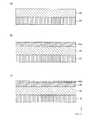
先ず、図2(a)に示すように、表示パネル10は、基板101をベースとして形成されている。そして、基板101上には、TFT(薄膜トランジスタ)102が形成され、基板101とTFT102との組み合わせを以ってTFT基板103が構成される。2. Configuration of
First, as shown in FIG. 2A, the
TFT102は、ドレイン102aを含む電極と半導体層(図示を省略)と、パッシベーション膜102bなどから構成されている。
TFT基板103の上には、層間絶縁膜104が積層形成されており、TFT102における各ドレイン102aに対応してコンタクト孔が開けられている。コンタクト孔は、パッシベーション膜102bにも連通しており、ドレイン102aが層間絶縁膜104の底部に露出した状態となっている。The
An interlayer insulating
層間絶縁膜104上には、サブピクセル毎にアノード105が形成されている。アノード105は、コンタクト孔の内壁に沿っても形成されている、底部に露出するTFT102のドレイン102aに接続されている。アノード105の上には、酸化金属層であるホール注入層107が形成されている。
図2(a)に示すように、ホール注入層107上の一部には、バンク108が立設されている。図3に示すように、本実施の形態に係る表示装置10においては、バンク108は、X軸方向に延伸する複数条の要素108aとY軸方向に延伸する複数条の要素108bとが一体に形成されてなるものであって、これらにより囲繞される各部分がサブピクセル100a,100b,100cとなり、Y軸方向に隣接する3つのサブピクセル100a,100b,100cの組み合わせを以って一つのピクセルを構成している。On the
As shown in FIG. 2A, a
図2(a)に戻って、バンク108により囲繞される各凹部内には、ホール輸送(IL)層109および有機発光層110が順に積層形成されている。そして、有機発光層110およびバンク108を覆うように、電子輸送層111、カソード112、および封止層113が順に積層形成されている。図2(a)に示すように、ホール注入層107、ホール輸送層109、有機発光層110、および電子輸送層112の積層体が、表示パネル10における機能層となる。 Returning to FIG. 2A, a hole transport (IL)
なお、各構成要素の形成に用いる材料は、例えば、次のようなものとすることができる。
(i) 基板101
基板101は、例えば、無アルカリガラス、ソーダガラス、無蛍光ガラス、燐酸系ガラス、硼酸系ガラス、石英、アクリル系樹脂、スチレン系樹脂、ポリカーボネート系樹脂、エポキシ系樹脂、ポリエチレン、ポリエステル、シリコーン系樹脂、又はアルミナ等の絶縁性材料をベースとして形成されている。In addition, the material used for formation of each component can be made into the following, for example.
(I)
The
(ii) 層間絶縁膜104
層間絶縁膜104は、例えば、ポリイミド、ポリアミド、アクリル系樹脂材料などの有機化合物を用い形成されている。
(iii) アノード105
アノード105は、アルミニウム(Al)若しくは銀(Ag)、またはそれらを含む合金から構成されている。トップエミッション型の本実施の形態に係る表示パネル10の場合には、その表面部が高い光反射性を有することが好ましい。本実施の形態では、一例として、アルミニウム(Al)の合金を用いアノード105が構成されている。(Ii)
The
(Iii)
The
(iv) ホール注入層107
ホール注入層107は、タングステン(W)またはモリブデン(Mo)またはニッケル(Ni)の酸化物からなる層である。上記のように、金属の酸化物からなるホール注入層107を採用する本実施の形態に係る表示パネル10では、ホールを安定的に生成し、またはホールの生成を補助して、有機発光層110に対しホールを注入する機能を有し、大きな仕事関数を有する。(Iv)
The
ここで、上記のように、ホール注入層107を遷移金属の酸化物から構成する本実施の形態の場合には、複数の酸化数をとるためこれにより複数の準位をとることができ、その結果、ホール注入が容易になり駆動電圧を低減することができる。特に、酸化タングステン(WOx)を用いることが、ホールを安定的に注入し、且つ、ホールの生成を補助するという機能を有するという観点から望ましい。 Here, as described above, in the case of the present embodiment in which the
ここで、本実施の形態では、一例として、タングステン(W)の酸化物WOxからホール注入層が構成されており、その層中の少なくとも一部において、酸化物WOxにおける酸素の組成比が化学量論比よりも小さい(x<3)。即ち、ホール注入層107は、酸素欠損状態の酸化物WOxから少なくとも一部が構成されている。
(v) バンク108
バンク108は、樹脂等の有機材料を用い形成されており絶縁性を有する。バンク108の形成に用いる有機材料の例としては、アクリル系樹脂、ポリイミド系樹脂、ノボラック型フェノール樹脂等があげられる。バンク106は、有機溶剤耐性を有することが好ましい。さらに、バンク108は、製造工程中において、エッチング処理、ベーク処理など施されることがあるので、それらの処理に対して過度に変形、変質などをしないような耐性の高い材料で形成されることが好ましい。また、撥水性をもたせるために、表面をフッ素処理することもできる。Here, in this embodiment, as an example, a hole injection layer is formed from an oxide WOx of tungsten (W), and at least a part of the layer has a chemical composition ratio of oxygen in the oxide WOx. Smaller than the theoretical ratio (x <3). That is, the
(V)
The
なお、バンク108を親液性の材料を用い形成した場合には、バンク108の表面と有機発光層110の表面との親液性/撥液性の差異が小さくなり、有機発光層110を形成するために有機物質を含んだインクを、バンク108の囲繞により構成される凹部内に選択的に保持させることが困難となってしまうためである。
さらに、バンク108の構造については、図2(a)に示すような一層構造だけでなく、二層以上の多層構造を採用することもできる。この場合には、層毎に上記材料を組み合わせることもできるし、層毎に無機材料と有機材料とを用いることもできる。When the
Furthermore, as for the structure of the
(vi) ホール輸送層109
ホール輸送層109は、親水基を備えない高分子化合物を用い形成されている。例えば、ポリフルオレンやその誘導体、あるいはポリアリールアミンやその誘導体などの高分子化合物であって、親水基を備えないものなどを用いることができる。
(vii) 有機発光層110
有機発光層110は、上述のように、ホールと電子とが注入され再結合されることにより励起状態が生成され発光する機能を有する。有機発光層110の形成に用いる材料は、湿式印刷法を用い製膜できる発光性の有機材料を用いることが必要である。(Vi)
The
(Vii) Organic
As described above, the organic
具体的には、例えば、特許公開公報(日本国・特開平5−163488号公報)に記載のオキシノイド化合物、ペリレン化合物、クマリン化合物、アザクマリン化合物、オキサゾール化合物、オキサジアゾール化合物、ペリノン化合物、ピロロピロール化合物、ナフタレン化合物、アントラセン化合物、フルオレン化合物、フルオランテン化合物、テトラセン化合物、ピレン化合物、コロネン化合物、キノロン化合物及びアザキノロン化合物、ピラゾリン誘導体及びピラゾロン誘導体、ローダミン化合物、クリセン化合物、フェナントレン化合物、シクロペンタジエン化合物、スチルベン化合物、ジフェニルキノン化合物、スチリル化合物、ブタジエン化合物、ジシアノメチレンピラン化合物、ジシアノメチレンチオピラン化合物、フルオレセイン化合物、ピリリウム化合物、チアピリリウム化合物、セレナピリリウム化合物、テルロピリリウム化合物、芳香族アルダジエン化合物、オリゴフェニレン化合物、チオキサンテン化合物、アンスラセン化合物、シアニン化合物、アクリジン化合物、8−ヒドロキシキノリン化合物の金属錯体、2−ビピリジン化合物の金属錯体、シッフ塩とIII族金属との錯体、オキシン金属錯体、希土類錯体などの蛍光物質で形成されることが好ましい。 Specifically, for example, an oxinoid compound, a perylene compound, a coumarin compound, an azacoumarin compound, an oxazole compound, an oxadiazole compound, a perinone compound, and pyrrolopyrrole described in Japanese Patent Publication (JP-A-5-163488). Compound, naphthalene compound, anthracene compound, fluorene compound, fluoranthene compound, tetracene compound, pyrene compound, coronene compound, quinolone compound and azaquinolone compound, pyrazoline derivative and pyrazolone derivative, rhodamine compound, chrysene compound, phenanthrene compound, cyclopentadiene compound, stilbene compound , Diphenylquinone compound, styryl compound, butadiene compound, dicyanomethylenepyran compound, dicyanomethylenethiopyran compound, fluorene In compounds, pyrylium compounds, thiapyrylium compounds, serenapyrylium compounds, telluropyrylium compounds, aromatic ardadiene compounds, oligophenylene compounds, thioxanthene compounds, anthracene compounds, cyanine compounds, acridine compounds, 8-hydroxyquinoline compound metal complexes, 2- It is preferably formed of a fluorescent substance such as a metal complex of a bipyridine compound, a Schiff salt and a group III metal complex, an oxine metal complex, or a rare earth complex.
(viii) 電子輸送層111
電子輸送層111は、カソード112から注入された電子を有機発光層110へ輸送する機能を有し、例えば、オキサジアゾール誘導体(OXD)、トリアゾール誘導体(TAZ)、フェナンスロリン誘導体(BCP、Bphen)などを用い形成されている。
なお、電子輸送層111として、バリウム(Ba)などのアルカリ金属を用い、蒸着法等のドライプロセスを用いて成膜した層を採用することも可能である。(Viii)
The
Note that a layer formed using a dry process such as a vapor deposition method using an alkali metal such as barium (Ba) as the
(ix) カソード112
カソード112は、例えば、ITO(Indium Tin Oxide)若しくはIZO(Indium Zinc Oxide)などを用い形成される。本実施の形態のように、トップエミッション型の表示パネル10の場合においては、光透過性の材料で形成されることが好ましい。光透過性については、透過率が80[%]以上とすることが好ましい。(Ix)
The
(x) 封止層113
封止層113は、有機発光層110などの有機層が水分に晒されたり、空気に晒されたりすることを抑制する機能を有し、例えば、SiN(窒化シリコン)、SiON(酸窒化シリコン)などの材料を用い形成される。また、SiN(窒化シリコン)、SiON(酸窒化シリコン)などの材料を用い形成された層の上に、アクリル樹脂、シリコーン樹脂などの樹脂材料からなる封止樹脂層を設けてもよい。(X)
The
封止層113は、トップエミッション型である本実施の形態に係る表示パネル10の場合においては、光透過性の材料で形成されることが好ましい。
3.カソード105とホール注入層107との間の構成
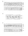
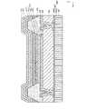
カソード105とホール注入層107との間の構成について、図2(b)、図4および図5を用い説明する。図2(b)は、図2(a)における一部(A部分)を拡大してします模式断面図である。In the case of the
3. Configuration Between
図2(b)に示すように、表示パネル10では、アノード105とホール注入層107との間に、アノード105およびホール注入層107の双方に接する状態で、混合層106が介挿されている。図4に示すように、混合層106は、アノード105の構成要素であるアルミニウム(Al)とホール注入層107の構成要素であるタングステン(W)と、酸素(O)とが混合された層である。 As shown in FIG. 2B, in the
図2(b)に戻って、混合層106の厚みt106は、10[nm]未満に規定されている。これは、酸化金属層である混合層106の厚みt106が10[nm]以上となる場合には、電気抵抗が大きくなり問題となる。よって、実デバイスとして採用することができるのは、10[nm]未満の厚みとなる。
混合層106の厚みt106については、上記のような理由から10[nm]未満であればよいが、例えば、3[nm]〜7[nm]の範囲内、好ましくは4[nm]〜5[nm]の範囲内である。Returning to FIG. 2B, the thickness t106 of the
The thickness t106 of the
図5(a)に示すように、混合層106においては、層中のアルミニウム(Al)が一様に分布しているのではなく、アノード105に接する側での濃度が高く、ホール注入層107に接する側に向けて漸減するような濃度勾配を有する。
逆に、図5(b)に示すように、混合層106におけるタングステン(W)は、ホール注入層107に接する側で濃度が高く、アノード105に接する側に向けて漸減するような濃度勾配を有する。As shown in FIG. 5A, in the
Conversely, as shown in FIG. 5B, the concentration of tungsten (W) in the
そして、混合層106中における酸化アルミニウム(AlOy)については、層中の少なくとも一部における酸素(O)の組成比yが化学量論比よりも小さくなっている(y<3/2)。即ち、本実施の形態に係る表示パネル10では、混合層106について、Al2O3よりも絶縁性が緩和された状態となっている。
なお、本実施の形態における酸化アルミニウム(AlOx)の、層中の少なくとも一部における酸素(O)の組成比yは、例えば、0.42である。As for aluminum oxide (AlOy) in the
In addition, the composition ratio y of oxygen (O) in at least a part of the layer of aluminum oxide (AlOx) in the present embodiment is, for example, 0.42.
4.製造方法
(i)有機EL表示装置1の製造方法の概要
本実施の形態に係る有機EL表示装置1の製造方法の概要について、図6を用い説明する。
図6に示すように、先ず、TFT基板103を準備し(ステップS1)、層上に層間絶縁膜104を積層形成する(ステップS2)。上述の通り、層間絶縁膜104におけるTFT102のドレイン102a上の各箇所にコンタクト孔をあけた後、アノード105を形成する。4). Manufacturing Method (i) Overview of Manufacturing Method of Organic EL Display Device 1 An overview of a manufacturing method of the organic EL display device 1 according to the present embodiment will be described with reference to FIG.
As shown in FIG. 6, first, a
アノード105の形成は、例えば、スパッタリング法や真空蒸着法などを用い金属膜(Al合金膜)を成膜した後、エッチングにより各サブピクセル単位に区画することによりなされる。
次に、アノード105の上に、酸化金属層(例えば、WOx)からなるホール注入層107を形成する(ステップS4)。ホール注入層107の形成には、例えば、スパッタリング法を用いる。具体的には、不活性ガスとしてのアルゴン(Ar)と酸素(O)との混合ガスをスパッタリング装置のチャンバー内に4[Pa]〜7[Pa]のガス圧を以って導入し、0.7[kW]〜1.5[kW]のパワーで成膜する。なお、チャンバー内に導入する混合ガスについては、全圧に対する酸素の分圧比を50[%]とする。The
Next, a
なお、本実施の形態におけるホール注入層107が、上記のようにタングステン(W)を含み、且つ、価電子帯で最も低い結合エネルギよりも1.8[eV]〜3.6[eV]低い結合エネルギ領域内に占有準位を有するものである。そして、ホール注入層107においては、紫外線光電子分光分析(UPS)スペクトルで、価電子帯が最も低い結合エネルギより1.8[eV]〜3.6[eV]低い結合エネルギ領域内に、隆起した形状を有し、また、X線光電子分光分析(XPS)スペクトルにおいて、価電子帯で最も低い結合エネルギより1.8[eV]〜3.6[eV]低い結合エネルギ領域内に、隆起した形状を有する。 Note that the
ここで、ホール注入層107の形成により、図2(b)に示すように、アノード105とホール注入層107との界面部分に混合層106が形成されることになるが、これについては後述する。
なお、アノード105およびホール注入層107の形成には、上記の他に次のような方法を採用することもできる。Here, by forming the
In addition to the above, the following method can also be adopted for forming the
先ず、金属(例えば、Al合金)からなる膜を成膜し、次に酸化金属(例えば、WOX)からなる膜を成膜する。
次に、金属膜および酸化金属膜を熱処理(例えば、230[℃]以上の温度で焼成処理)し、その後にエッチングにより各サブピクセル単位に区画することで、アノード105およびホール注入層107を形成することができる。First, a film made of a metal (for example, an Al alloy) is formed, and then a film made of a metal oxide (for example, WOx ) is formed.
Next, the metal film and the metal oxide film are heat-treated (for example, baked at a temperature of 230 [° C.] or higher), and then divided into sub-pixel units by etching, whereby the
次に、ホール注入層107の上にバンク108を形成する(ステップS5)。バンク108の形成は、先ず、スピンコート法等により、感光性樹脂成分とフッ素成分とを含む材料を用いてバンク材料層を積層形成し、その後に、マスク露光および現像処理を施すことによりバンク材料層をパターニングすることによりなされる。
なお、バンク108の形成に際しては、例えば、全波長で露光し、TMAH現像液を用いパドル現像若しくはスプレー現像を行う。その後に、純水を用いたリンス処理を行う。そして、焼成することによりバンク108を形成することができる。当該バンク108の形成条件は、一例として、サブピクセルのサイズが、長辺方向が300[μm]で、短辺方向が100[μm]のものであり、形成しようとするサブピクセルのサイズによりバンク108の形成条件は適宜変更が必要である。Next, the
In forming the
次に、バンク108の囲繞により構成された各凹部にホール輸送層109および有機発光層110を順に積層形成する(ステップS6,S7)。ホール輸送層109および有機発光層110の各形成は、例えば、印刷法を用い成膜した後、焼成することでなされる。
次に、有機発光層110の上、およびバンク108の露出面の上に、電子輸送層111、カソード112、および封止層113を順に積層形成する(ステップS8,S9,S10)。そして、カラーフィルタ層が形成されたCF基板を貼り合わせた後(ステップS11)、駆動制御部20を接続する(ステップS12)。Next, the
Next, the
最後に、有機EL表示装置1に対してエージング処理を施す(ステップS13)。エージング処理は、例えば、処理前におけるホール注入性に対して、ホールの移動度が1/10以下となるまで通電処理を行うことでなされる。より具体的には、実際の装置使用時における輝度以上であって、且つ、その3倍以下の輝度となるように、0[min.]を超え30[min.]以内の間、通電処理を実行することによりエージングがなされる。 Finally, an aging process is performed on the organic EL display device 1 (step S13). The aging process is performed, for example, by performing an energization process until the hole mobility becomes 1/10 or less with respect to the hole injection property before the process. More specifically, 0 [min.] Is set so that the luminance is equal to or higher than the luminance at the time of actual use of the apparatus and is three times or less. ] Over 30 [min. ], The aging is performed by executing the energization process.
以上のようにして有機EL表示装置1が完成する。
(2)混合層106の形成
次に、アノード105とホール注入層107との界面部分への混合層106の形成について、図7および図8を用い説明する。
先ず、図7(a)に示すように、TFT基板103の上に層間絶縁膜104を形成する。これについては、上述の通りである。なお、TFT102、および層間絶縁膜104におけるコンタクト孔などの図示については省略している。The organic EL display device 1 is completed as described above.
(2) Formation of
First, as shown in FIG. 7A, an
次に、図7(b)に示すように、層間絶縁膜104の上に、アルミニウム(Al)の合金からなるアノード準備層1050を形成する。なお、上記のように、この後にアノード準備層1050をエッチングによりパターニングする。
次に、アノード準備層1050のパターニングの後に、当該ワークをスパッタリング装置のチャンバー内に入れ、アルゴン(Ar)と酸素(O)との混合ガスを導入しながら、タングステン(W)の酸化物(WOx)からなるホール注入準備層1070を積層形成する。混合ガスの導入を開始した直後において、図7(c)に示すように、アノード準備層1050のZ軸方向上面部分にアルミニウム(Al)の酸化金属層1060が形成される。この状態における酸化金属層1060は、酸素の組成比が化学量論比と同一あるいは略同一の状態であると考えられる。即ち、酸化金属層1060がAlOyであるときに、酸素の組成比yが略3/2となっていると考えられる。Next, as shown in FIG. 7B, an
Next, after patterning the
なお、アノード準備層1050の上面部分が酸化金属層1060となることにより、残りの部分がアノード105となる(図7(c)を参照)。
図8(a)に示すように、スパッタリング法によるホール注入準備層1070の成膜を進めて行くと、酸化金属層1061の酸素(O)が酸素欠損状態のホール注入準備層1071へと引き込まれ、逆に、ホール注入準備層1071から酸化金属層1061へとタングステン(W)が注入されることになると考えられる(図8(b)を参照)。The upper surface portion of the
As shown in FIG. 8A, when the film formation of the hole
最後に、熱処理を加えることで、更に酸素(O)が酸素欠損状態のホール注入準備層1071へと拡散(熱拡散)され、酸化金属層1061の絶縁性が緩和される。
以上のような過程を経て、図8(c)に示すように、アノード105およびホール注入層107と、その間に介挿され、アノード105およびホール注入層107の双方に対して接する混合層106が形成される。よって、混合層106では、アルミニウム(Al)と酸素(O)とタングステン(W)とが混在した状態となっている(図4を参照)。そして、AlOyにおける酸素の組成比yは、化学量論比よりも小さくなり(y<3/2)、例えば、“0.42”となる。Finally, by applying heat treatment, oxygen (O) is further diffused (thermally diffused) into the hole-
Through the above process, as shown in FIG. 8C, the
なお、形成されるホール注入層107においては、タングステン(W)の酸化物(WOx)からなり、その層中の少なくとも一部における酸素の組成比xが化学量論比よりも小さくなっている(x<3)。
5.効果
本発明の実施の形態に係る表示パネル10では、アノード105とホール注入層107との間に、その両方と接するように酸化金属層である混合層106が介挿されている。この混合層106は、アノード105の構成金属であるアルミニウム(Al)とホール注入層107の構成金属であるタングステン(W)と、スパッタリングの際に取り込まれた酸素(O)とを要素として構成されている。この混合層106は、上述のように、アノード105の上にホール注入層107を形成する際に、その界面部分に形成される層である。このため、本実施の形態では、アノード105とホール注入層107との間に、従来技術のようなキャップ層(ITOなどからなる層)を設けていない。よって、本実施の形態に係る表示パネル10では、キャビティー設計における自由度が高い。The formed
5. Effect In the
また、本実施の形態に係る表示パネル10では、混合層106を構成するAlOyにおける酸素の組成比yが、層中の少なくとも一部で化学量論比よりも小さい(y<3/2)ので、酸化物であるにもかかわらず絶縁性が緩和された状態にある(ホール注入性を有する)とともに、アノード105とホール注入層107との間に混合層106を介挿することにより、アノード105からホール注入層107へ注入されるホール量が制限され、有機発光層110に注入されるホールと電子の注入バランスをとることが可能となっている。よって、本実施の形態に係る表示パネル10では、高い発光効率を有し、且つ、長寿命である。 In the
図9に示すように、混合層の介挿がない比較例の寿命がT1であるのに対して、本実施の形態では、寿命がT2となる。例えば、T1とT2との関係は次のようになるものと考えられる。
[数1]T2=k×T1
[数2]1.1<k<1.3
以上より、本実施の形態に係る表示パネル10およびこれを構成要素として備える有機EL表示装置1
では、キャビティー設計における高い自由度を得ることができるとともに、キャリアバランスの崩れを抑制することで、高い発光効率を有し、且つ、長寿命である。As shown in FIG. 9, in the present embodiment, the lifetime is T2 , whereas the lifetime of the comparative example without the mixed layer is T1 . For example, the relationship between T1 and T2 is considered as follows.
[Formula 1] T2 = k × T1
[Formula 2] 1.1 <k <1.3
As described above, the
Then, while being able to obtain a high degree of freedom in the cavity design, by suppressing the collapse of the carrier balance, it has high luminous efficiency and a long life.
[実施の形態2]
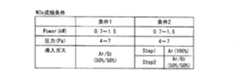
実施の形態2に係る表示パネルの製造方法について、図10を用い説明する。図10は、ホール注入層を形成する際のスパッタリング条件を示す表である。図10における「条件1」が上記実施の形態1に係るホール注入層107の形成に用いたスパッタリング条件であり、「条件2」が本実施の形態に係るホール注入層の形成に用いるスパッタリング条件である。なお、本実施の形態に係る表示パネルの製造方法は、ホール注入層の形成に係るスパッタリング条件を除き、上記実施の形態1と同様であるので、その説明を省略する。[Embodiment 2]
A method for manufacturing a display panel according to Embodiment 2 will be described with reference to FIGS. FIG. 10 is a table showing the sputtering conditions for forming the hole injection layer. “Condition 1” in FIG. 10 is a sputtering condition used for forming the
図10に示すように、本実施の形態に係るスパッタリング条件(条件2)は、パワーおよび圧力が上記実施の形態1に係るスパッタリング条件(条件1)と同一であり、チャンバー内へのガスの導入の仕方が上記実施の形態1とは異なっている。具体的には、本実施の形態に係るスパッタリング条件(条件2)では、スパッタリングの期間前期(ステップ1)では、不活性ガスであるアルゴン(Ar)のみを導入し、続いて期間後期(ステップ2)では、アルゴン(Ar)と酸素(O)との混合ガスを導入する。この期間後期に導入する混合ガスは、全圧に対する酸素(O)の分圧比が、上記同様、50[%]である。 As shown in FIG. 10, the sputtering conditions (condition 2) according to the present embodiment have the same power and pressure as the sputtering conditions (condition 1) according to the first embodiment, and the introduction of gas into the chamber. This is different from the first embodiment. Specifically, in the sputtering conditions (condition 2) according to the present embodiment, only the inert gas argon (Ar) is introduced in the first half of the sputtering period (step 1), followed by the second half of the period (step 2). ), A mixed gas of argon (Ar) and oxygen (O) is introduced. The mixed gas introduced later in this period has a partial pressure ratio of oxygen (O) to the total pressure of 50 [%] as described above.
このように、スパッタリング期間の期間前期でアルゴン(Ar)のみを導入して、その後、期間後期に酸素(O)を含む混合ガスを導入することとすれば、形成される混合層の組成AlOyでの酸素の組成比yが上記実施の形態1に係る混合層106よりも小さくなる。例えば、y=0.33程度となるものと考えられる。
また、形成される混合層の層厚に関しても、上記実施の形態1の混合層106よりも薄くすることができ、導電性を確保するという観点から更に優れていると考えられる。Thus, if only argon (Ar) is introduced in the first half of the sputtering period, and then a mixed gas containing oxygen (O) is introduced in the second half of the period, the composition of the mixed layer formed is AlOy. The oxygen composition ratio y becomes smaller than that of the
Further, the thickness of the formed mixed layer can also be made thinner than that of the
[変形例]
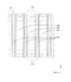
変形例に係る表示パネル30の構成について、図11を用い説明する。図11では、変形例に係るバンク308の構成を示し、それ以外の構成については上記実施の形態1に係る表示パネル10およびそれを備える有機EL表示装置1と同一であるので、図示および以下での説明を省略する。[Modification]
A configuration of the
図11に示すように、本変形例に係る表示パネル30では、それぞれX軸方向に延伸形成され、互いに並行する複数のライン状のバンク308を有する。そして、隣り合うバンク308間の領域をX軸方向に分割するように画素規制層314が形成されている。
本変形例に係る表示パネル30では、ライン状のバンク308で区画される凹部毎に、サブピクセル300a,300b,300cが形成されている。As shown in FIG. 11, the
In the
なお、表示パネル30における積層構成については、上記実施の形態1と同様であって、ホール注入層の形成においては上記実施の形態2に係るスパッタリング条件を採用することもできる。
本変形例に係る表示パネル30においても、上記実施の形態1に係る表示パネル10と同様の積層構成を有するので、上記同様の効果を奏することができる。Note that the laminated structure of the
Since the
[その他の事項]
上記実施の形態1,2では、アノード105を、アルミニウム(Al)またはアルミニウム合金(Al合金)を用い形成することとしたが、これ以外にも光反射性を有する金属電極を採用することができる。例えば、銀(Ag)や銀合金(Ag合金)などを用い、アノードを形成することもできる。[Other matters]
In the first and second embodiments, the
また、上記実施の形態1,2では、有機EL表示装置1を一例として採用したが、これ以外の有機EL素子に対しても適用することができ、その場合にも上記同様の効果を得ることができる。例えば、信号などに本発明の構成を採用することができる。
また、上記実施の形態1では、混合層106が、アノード105とホール注入層107との界面部分において、それらと全表面に対して接するように形成することとしたが、少なくとも一部に対して接触して形成されることとしても、上記効果を少なくとも一部において享受することが可能となる。In the first and second embodiments, the organic EL display device 1 is used as an example. However, the present invention can be applied to other organic EL elements, and the same effect as described above can be obtained. Can do. For example, the configuration of the present invention can be employed for a signal or the like.
In the first embodiment, the
また、上記実施の形態1,2では、アノード、混合層、ホール注入層、ホール輸送層、有機発光層、電子輸送層、カソードの順で積層されてなる積層構成を採用することとしたが、アノード、混合層、ホール注入層、有機発光層、およびカソードを除く層については、適宜省略することも可能であり、また、他の層を介挿させることも可能である。
また、上記実施の形態1,2では、ホール注入層107の構成として、タングステン(W)の酸化物WOxを一例として採用したが、これ以外にも、モリブデン(Mo)やニッケル(Ni)の酸化物からなる層とすることもできる。この場合においても、上記同様にアノードとの間に混合層ができ、その場合には、アルミニウム(Al)と酸素(O)とモリブデン(Mo)の混合層、あるいは、アルミニウム(Al)と酸素(O)とニッケル(Ni)との混合層となる。また、アノードとして銀(Ag)あるいはその合金を採用する場合には、銀(Ag)と酸素(O)とモリブデン(Mo)の混合層、あるいは、銀(Ag)と酸素(O)とニッケル(Ni)との混合層となる。このような構成とする場合においても、上記同様の効果を得ることができる。In the first and second embodiments, the laminated structure in which the anode, the mixed layer, the hole injection layer, the hole transport layer, the organic light emitting layer, the electron transport layer, and the cathode are stacked in this order is adopted. The layers other than the anode, the mixed layer, the hole injection layer, the organic light emitting layer, and the cathode can be omitted as appropriate, and other layers can be interposed.
In the first and second embodiments, as the structure of the
また、図10に示すスパッタリング条件は、一例として示すものであって、パネルサイズなどや形成しようとするホール注入層の層厚などに応じて適宜変更することが可能である。
また、上記実施の形態1,2では、有機EL素子の一例として、有機EL表示装置を採用したが、本発明は、これに限定されない。照明装置などの素子としても適用が可能である。Moreover, the sputtering conditions shown in FIG. 10 are shown as an example, and can be appropriately changed according to the panel size and the like, the layer thickness of the hole injection layer to be formed, and the like.
In the first and second embodiments, the organic EL display device is employed as an example of the organic EL element, but the present invention is not limited to this. The present invention can also be applied as an element such as a lighting device.
本発明は、駆動時間の長短にかかわらず、高い発光効率を有するとともに、長寿命な有機EL素子を実現するのに有用である。 The present invention is useful for realizing an organic EL element having high light emission efficiency and a long lifetime regardless of the driving time.
1.有機EL表示装置
10,30.表示パネル
20.駆動制御部
21〜24.駆動回路
25.制御回路
100a,100b,100c,300a,300b,300c.サブピクセル
101.基板
102.TFT
103.TFT基板
104.層間絶縁膜
106.混合層
107.ホール注入層
108.バンク
109.ホール輸送層
110.有機発光層
111.電子輸送層
113.封止層
114.機能層
314.画素規制層
1050.アノード準備層
1060,1061.酸化金属層
1070,1071.ホール注入準備層1. Organic
103.
Claims (17)
Translated fromJapanese前記陽極の上方に形成され、タングステンまたはモリブデンまたはニッケルからなる金属MBの酸化物である第1酸化物MBOxを含み、その層中の少なくとも一部における第1酸化物MBOx中の酸素の組成比xが化学量論比よりも小さい第1酸化金属層と、
前記陽極と前記第1酸化金属層との間に、当該陽極および第1酸化金属層の双方に接して形成され、前記金属MAと同一の金属の酸化物である第2酸化物MAOyを含み、その層中の少なくとも一部における第2酸化物MAOy中の酸素の組成比yが化学量論比よりも小さい第2酸化金属層と、
前記第1酸化金属層の上方設けられ、有機発光材料を含む発光層と、
前記発光層の上方に設けられた陰極と、
を有する
ことを特徴とする有機EL素子。An anode comprising a metal MA made of aluminum or silver, or an alloy thereof,
A first oxide MB Ox which is formed above the anode and is an oxide of a metal MB made of tungsten, molybdenum or nickel, and in the first oxide MB Ox in at least a part of the layer; A first metal oxide layer having a composition ratio x of oxygen smaller than the stoichiometric ratio;
A second oxide MA Oy is formed between the anode and the first metal oxide layer so as to be in contact with both the anode and the first metal oxide layer and is an oxide of the same metal as the metal MA.A second metal oxide layer in which the composition ratio y of oxygen in the second oxide MA Oy in at least a part of the layer is smaller than the stoichiometric ratio;
A light emitting layer provided above the first metal oxide layer and including an organic light emitting material;
A cathode provided above the light emitting layer;
An organic EL element comprising:
請求項1記載の有機EL素子。Wherein the second metal oxide layer, said metal MB same metal as or organic EL element according to claim 1, wherein it contains also their oxides.
請求項1または請求項2記載の有機EL素子。The same metal as the metal MA in the second metal oxide layer, toward the side in contact with the anode on the side in contact with the first metal oxide layer contains a gradient of its concentration gradually decreases according Item 3. The organic EL device according to Item 1 or Item 2.
請求項1から請求項3の何れか記載の有機EL素子。The organic EL element according to any one of claims 1 to 3, wherein a thickness of the second metal oxide layer is less than 10 nm.
請求項1から請求項3の何れか記載の有機EL素子。The organic EL element according to any one of claims 1 to 3, wherein a thickness of the second metal oxide layer is 3 nm or more and 7 nm or less.
請求項1から請求項3の何れか記載の有機EL素子。The organic EL element according to any one of claims 1 to 3, wherein a thickness of the second metal oxide layer is 4 nm or more and 5 nm or less.
前記金属MBは、タングステンである
請求項1から請求項6の何れか記載の有機EL素子。It said metal MA is aluminum,
Said metal MB, the organic EL device according to any one of claims 1 to 6 is tungsten.
請求項7記載の有機EL素子。The organic EL element according to claim 7, wherein in the first metal oxide layer, a composition ratio x of oxygen in the first oxide MB Ox in at least a part of the layer is smaller than a stoichiometric ratio.
請求項7または請求項8記載の有機EL素子。The organic EL element according to claim 7 or 8, wherein in the second metal oxide layer, a composition ratio y of oxygen in the second oxide MA Oy in at least a part of the layer is smaller than a stoichiometric ratio. .
請求項7または請求項8記載の有機EL素子。The organic EL element according to claim 7 or 8, wherein the composition ratio y is 0.42 or less.
請求項1から請求項10の何れか記載の有機EL素子。The organic EL element according to any one of claims 1 to 10, wherein the first metal oxide layer and the second metal oxide layer have conductivity.
前記陽極準備層上に、少なくとも一部期間で酸素を導入する薄膜成膜法を用い、タングステンまたはモリブデンまたはニッケルからなる金属MBの酸化物である第1酸化物MBOxを含む第1酸化金属層を形成し、
前記第1酸化金属層の上方に、有機発光材料を含む発光層を形成し、
前記発光層の上方に陰極を設け、
前記第1酸化金属層の形成中において、
前記陽極準備層と前記第1酸化金属層との界面部分に、当該陽極準備層および第1酸化金属層の双方に接する状態で、前記金属MAの第2酸化物MAOyを含み、その層中の少なくとも一部における前記第2酸化物MAOy中の酸素の組成比yが化学量論比よりも小さい第2酸化金属層が形成され、
前記第1酸化金属層の形成後において、
前記陽極準備層から前記第2酸化金属層を除いた部分が陽極となり、
前記第1酸化金属層では、その層中の少なくとも一部における酸素の組成比xが化学量論比よりも小さくなる
ことを特徴とする有機EL素子の製造方法。Aluminum or silver, or to form an anode preparation layer comprising metal elements MA consisting of alloys,
The anode preparation layer, at least a partial period oxygen thin film forming method using the introduction with a first oxide comprising a first oxide MB Ox is an oxide of a metal MB consisting of tungsten or molybdenum or nickel Forming a metal layer,
Forming a light emitting layer including an organic light emitting material on the first metal oxide layer;
A cathode is provided above the light emitting layer,
During the formation of the first metal oxide layer,
The interface between the anode preparation layer and the first metal oxide layer, in a state in contact with both the anode preparation layer and the first metal oxide layer comprises a second oxide MA Oy of said metal MA, theA second metal oxide layer in which the composition ratio y of oxygen in the second oxide MA Oy in at least a part of the layer is smaller than the stoichiometric ratio is formed;
After forming the first metal oxide layer,
The portion obtained by removing the second metal oxide layer from the anode preparation layer is an anode,
In the first metal oxide layer, the composition ratio x of oxygen in at least a part of the layer is smaller than the stoichiometric ratio.
請求項12記載の有機EL素子の製造方法。In the formation of the first metal oxide layer, a mixed gas of an inert gas and oxygen is introduced over the entire period.
The manufacturing method of the organic EL element ofClaim 12 .
請求項12記載の有機EL素子の製造方法。In forming the first metal oxide layer, only an inert gas is introduced in the first half of the period, and a mixed gas of inert gas and oxygen is introduced in the second half of the period.
The manufacturing method of the organic EL element ofClaim 12 .
請求項12から請求項14の何れか記載の有機EL素子の製造方法。A heat treatment is performed after forming the first metal oxide layer.
The method for manufacturing an organic EL device according to any one ofclaims 12to14.
前記金属MBとして、タングステンを用いる
請求項12から請求項15の何れか記載の有機EL素子の製造方法。As the metal MA, with aluminum,
As the metal MB, using tungsten
The method for manufacturing an organic EL device accordingto any one ofclaims 15claim 12.
請求項12から請求項16の何れか記載の有機EL素子の製造方法。The thickness of the second metal oxide layer is less than 10 nm.
The method for manufacturing an organic EL device of any one ofclaims 16claim 12.
Priority Applications (1)
| Application Number | Priority Date | Filing Date | Title |
|---|---|---|---|
| JP2012019748AJP5861961B2 (en) | 2012-02-01 | 2012-02-01 | Organic EL device and manufacturing method thereof |
Applications Claiming Priority (1)
| Application Number | Priority Date | Filing Date | Title |
|---|---|---|---|
| JP2012019748AJP5861961B2 (en) | 2012-02-01 | 2012-02-01 | Organic EL device and manufacturing method thereof |
Publications (2)
| Publication Number | Publication Date |
|---|---|
| JP2013161804A JP2013161804A (en) | 2013-08-19 |
| JP5861961B2true JP5861961B2 (en) | 2016-02-16 |
Family
ID=49173850
Family Applications (1)
| Application Number | Title | Priority Date | Filing Date |
|---|---|---|---|
| JP2012019748AActiveJP5861961B2 (en) | 2012-02-01 | 2012-02-01 | Organic EL device and manufacturing method thereof |
Country Status (1)
| Country | Link |
|---|---|
| JP (1) | JP5861961B2 (en) |
Families Citing this family (3)
| Publication number | Priority date | Publication date | Assignee | Title |
|---|---|---|---|---|
| JPWO2015182130A1 (en)* | 2014-05-30 | 2017-04-20 | 株式会社Joled | Organic EL element and organic EL light emitting device |
| JP7231487B2 (en)* | 2019-05-30 | 2023-03-01 | 株式会社神戸製鋼所 | Reflective anode electrode and manufacturing method thereof, thin film transistor substrate, organic EL display, and sputtering target |
| CN114695747A (en)* | 2020-12-31 | 2022-07-01 | Tcl科技集团股份有限公司 | Composite material, preparation method thereof and light emitting diode |
Family Cites Families (7)
| Publication number | Priority date | Publication date | Assignee | Title |
|---|---|---|---|---|
| US7560175B2 (en)* | 1999-12-31 | 2009-07-14 | Lg Chem, Ltd. | Electroluminescent devices with low work function anode |
| JP5063007B2 (en)* | 2006-02-06 | 2012-10-31 | 富士フイルム株式会社 | Organic electroluminescence device |
| JP2007335737A (en)* | 2006-06-16 | 2007-12-27 | Matsushita Electric Ind Co Ltd | Organic electroluminescent device and manufacturing method thereof |
| JP4931858B2 (en)* | 2008-05-13 | 2012-05-16 | パナソニック株式会社 | Method for manufacturing organic electroluminescent device |
| TWI491087B (en)* | 2009-08-26 | 2015-07-01 | Univ Nat Taiwan | Suspension or solution of transition metal oxide for organic photoelectric element, preparation method and application thereof |
| JP2011091093A (en)* | 2009-10-20 | 2011-05-06 | Panasonic Corp | Organic el element |
| JP5543441B2 (en)* | 2010-06-28 | 2014-07-09 | パナソニック株式会社 | ORGANIC LIGHT EMITTING ELEMENT AND ITS MANUFACTURING METHOD, ORGANIC DISPLAY PANEL, ORGANIC DISPLAY DEVICE |
- 2012
- 2012-02-01JPJP2012019748Apatent/JP5861961B2/enactiveActive
Also Published As
| Publication number | Publication date |
|---|---|
| JP2013161804A (en) | 2013-08-19 |
Similar Documents
| Publication | Publication Date | Title |
|---|---|---|
| JP5543441B2 (en) | ORGANIC LIGHT EMITTING ELEMENT AND ITS MANUFACTURING METHOD, ORGANIC DISPLAY PANEL, ORGANIC DISPLAY DEVICE | |
| JP4659141B1 (en) | LIGHT EMITTING ELEMENT, MANUFACTURING METHOD THEREOF, AND LIGHT EMITTING DEVICE | |
| JP6233888B2 (en) | Organic light emitting device and manufacturing method thereof | |
| JP5574456B2 (en) | LIGHT EMITTING ELEMENT, MANUFACTURING METHOD THEREOF, AND LIGHT EMITTING DEVICE | |
| JP6337111B2 (en) | Organic light emitting device and display device | |
| JP6142213B2 (en) | ORGANIC EL ELEMENT AND METHOD FOR PRODUCING ORGANIC EL ELEMENT | |
| JP6336042B2 (en) | ORGANIC EL ELEMENT AND METHOD FOR PRODUCING ORGANIC EL ELEMENT | |
| JP6340616B2 (en) | Organic EL element and organic EL display panel | |
| WO2012017492A1 (en) | Light emitting element, method for manufacturing same, and light emitting device | |
| JP2016091841A (en) | Organic light-emitting device and organic display device | |
| JP6332769B2 (en) | Organic light-emitting devices and organic display devices | |
| JP5861961B2 (en) | Organic EL device and manufacturing method thereof | |
| JP6159981B2 (en) | LIGHT EMITTING ELEMENT, DISPLAY DEVICE, AND LIGHT EMITTING ELEMENT MANUFACTURING METHOD | |
| WO2015182130A1 (en) | Organic el element and organic el light-emitting device | |
| US10581019B2 (en) | Organic EL element having reduced electric power consumption by optimizing film thicknesses thereof and method of manufacturing same | |
| JP2016110904A (en) | Method for manufacturing organic light-emitting element and organic light-emitting element | |
| JP5939564B2 (en) | Manufacturing method of organic EL element | |
| JP2021072416A (en) | Self-luminous element, self-luminous display panel, and manufacturing method of self-luminous element | |
| JP2016100150A (en) | Manufacturing method of organic light-emitting element and organic light-emitting element | |
| WO2015129212A1 (en) | Electronic device and method for manufacturing same |
Legal Events
| Date | Code | Title | Description |
|---|---|---|---|
| RD02 | Notification of acceptance of power of attorney | Free format text:JAPANESE INTERMEDIATE CODE: A7422 Effective date:20140606 | |
| A621 | Written request for application examination | Free format text:JAPANESE INTERMEDIATE CODE: A621 Effective date:20141225 | |
| A711 | Notification of change in applicant | Free format text:JAPANESE INTERMEDIATE CODE: A712 Effective date:20150205 | |
| A977 | Report on retrieval | Free format text:JAPANESE INTERMEDIATE CODE: A971007 Effective date:20150930 | |
| A131 | Notification of reasons for refusal | Free format text:JAPANESE INTERMEDIATE CODE: A131 Effective date:20151006 | |
| A521 | Request for written amendment filed | Free format text:JAPANESE INTERMEDIATE CODE: A523 Effective date:20151014 | |
| TRDD | Decision of grant or rejection written | ||
| A01 | Written decision to grant a patent or to grant a registration (utility model) | Free format text:JAPANESE INTERMEDIATE CODE: A01 Effective date:20151117 | |
| A61 | First payment of annual fees (during grant procedure) | Free format text:JAPANESE INTERMEDIATE CODE: A61 Effective date:20151211 | |
| R150 | Certificate of patent or registration of utility model | Ref document number:5861961 Country of ref document:JP Free format text:JAPANESE INTERMEDIATE CODE: R150 | |
| R250 | Receipt of annual fees | Free format text:JAPANESE INTERMEDIATE CODE: R250 | |
| R250 | Receipt of annual fees | Free format text:JAPANESE INTERMEDIATE CODE: R250 | |
| R250 | Receipt of annual fees | Free format text:JAPANESE INTERMEDIATE CODE: R250 | |
| R250 | Receipt of annual fees | Free format text:JAPANESE INTERMEDIATE CODE: R250 | |
| R250 | Receipt of annual fees | Free format text:JAPANESE INTERMEDIATE CODE: R250 | |
| S303 | Written request for registration of pledge or change of pledge | Free format text:JAPANESE INTERMEDIATE CODE: R316303 | |
| R350 | Written notification of registration of transfer | Free format text:JAPANESE INTERMEDIATE CODE: R350 | |
| S803 | Written request for registration of cancellation of provisional registration | Free format text:JAPANESE INTERMEDIATE CODE: R316803 | |
| R350 | Written notification of registration of transfer | Free format text:JAPANESE INTERMEDIATE CODE: R350 | |
| R250 | Receipt of annual fees | Free format text:JAPANESE INTERMEDIATE CODE: R250 | |
| S111 | Request for change of ownership or part of ownership | Free format text:JAPANESE INTERMEDIATE CODE: R313113 | |
| R350 | Written notification of registration of transfer | Free format text:JAPANESE INTERMEDIATE CODE: R350 |