JP5860917B2 - Printed wiring board - Google Patents
Printed wiring boardDownload PDFInfo
- Publication number
- JP5860917B2 JP5860917B2JP2014079092AJP2014079092AJP5860917B2JP 5860917 B2JP5860917 B2JP 5860917B2JP 2014079092 AJP2014079092 AJP 2014079092AJP 2014079092 AJP2014079092 AJP 2014079092AJP 5860917 B2JP5860917 B2JP 5860917B2
- Authority
- JP
- Japan
- Prior art keywords
- ground
- printed wiring
- wiring board
- pad
- pattern
- Prior art date
- Legal status (The legal status is an assumption and is not a legal conclusion. Google has not performed a legal analysis and makes no representation as to the accuracy of the status listed.)
- Active
Links
- 239000004020conductorSubstances0.000description44
- 239000012212insulatorSubstances0.000description19
- 239000000758substrateSubstances0.000description11
- 239000011248coating agentSubstances0.000description5
- 238000000576coating methodMethods0.000description5
- 238000005476solderingMethods0.000description5
- 230000004048modificationEffects0.000description3
- 238000012986modificationMethods0.000description3
- 230000000087stabilizing effectEffects0.000description3
- 230000000694effectsEffects0.000description2
- RYGMFSIKBFXOCR-UHFFFAOYSA-NCopperChemical compound[Cu]RYGMFSIKBFXOCR-UHFFFAOYSA-N0.000description1
- 239000000853adhesiveSubstances0.000description1
- 230000001070adhesive effectEffects0.000description1
- 239000011889copper foilSubstances0.000description1
- 238000004519manufacturing processMethods0.000description1
- 239000000463materialSubstances0.000description1
- 230000000149penetrating effectEffects0.000description1
- 230000002265preventionEffects0.000description1
- 239000011347resinSubstances0.000description1
- 229920005989resinPolymers0.000description1
- 238000005549size reductionMethods0.000description1
- 239000007787solidSubstances0.000description1
Images


Classifications
- H—ELECTRICITY
- H05—ELECTRIC TECHNIQUES NOT OTHERWISE PROVIDED FOR
- H05K—PRINTED CIRCUITS; CASINGS OR CONSTRUCTIONAL DETAILS OF ELECTRIC APPARATUS; MANUFACTURE OF ASSEMBLAGES OF ELECTRICAL COMPONENTS
- H05K1/00—Printed circuits
- H05K1/02—Details
- H05K1/0213—Electrical arrangements not otherwise provided for
- H05K1/0216—Reduction of cross-talk, noise or electromagnetic interference
- H05K1/0218—Reduction of cross-talk, noise or electromagnetic interference by printed shielding conductors, ground planes or power plane
- H05K1/0219—Printed shielding conductors for shielding around or between signal conductors, e.g. coplanar or coaxial printed shielding conductors
- H—ELECTRICITY
- H01—ELECTRIC ELEMENTS
- H01R—ELECTRICALLY-CONDUCTIVE CONNECTIONS; STRUCTURAL ASSOCIATIONS OF A PLURALITY OF MUTUALLY-INSULATED ELECTRICAL CONNECTING ELEMENTS; COUPLING DEVICES; CURRENT COLLECTORS
- H01R12/00—Structural associations of a plurality of mutually-insulated electrical connecting elements, specially adapted for printed circuits, e.g. printed circuit boards [PCB], flat or ribbon cables, or like generally planar structures, e.g. terminal strips, terminal blocks; Coupling devices specially adapted for printed circuits, flat or ribbon cables, or like generally planar structures; Terminals specially adapted for contact with, or insertion into, printed circuits, flat or ribbon cables, or like generally planar structures
- H01R12/50—Fixed connections
- H01R12/51—Fixed connections for rigid printed circuits or like structures
- H01R12/53—Fixed connections for rigid printed circuits or like structures connecting to cables except for flat or ribbon cables
- H—ELECTRICITY
- H01—ELECTRIC ELEMENTS
- H01R—ELECTRICALLY-CONDUCTIVE CONNECTIONS; STRUCTURAL ASSOCIATIONS OF A PLURALITY OF MUTUALLY-INSULATED ELECTRICAL CONNECTING ELEMENTS; COUPLING DEVICES; CURRENT COLLECTORS
- H01R13/00—Details of coupling devices of the kinds covered by groups H01R12/70 or H01R24/00 - H01R33/00
- H01R13/646—Details of coupling devices of the kinds covered by groups H01R12/70 or H01R24/00 - H01R33/00 specially adapted for high-frequency, e.g. structures providing an impedance match or phase match
- H01R13/6461—Means for preventing cross-talk
- H01R13/6471—Means for preventing cross-talk by special arrangement of ground and signal conductors, e.g. GSGS [Ground-Signal-Ground-Signal]
- H—ELECTRICITY
- H01—ELECTRIC ELEMENTS
- H01R—ELECTRICALLY-CONDUCTIVE CONNECTIONS; STRUCTURAL ASSOCIATIONS OF A PLURALITY OF MUTUALLY-INSULATED ELECTRICAL CONNECTING ELEMENTS; COUPLING DEVICES; CURRENT COLLECTORS
- H01R13/00—Details of coupling devices of the kinds covered by groups H01R12/70 or H01R24/00 - H01R33/00
- H01R13/646—Details of coupling devices of the kinds covered by groups H01R12/70 or H01R24/00 - H01R33/00 specially adapted for high-frequency, e.g. structures providing an impedance match or phase match
- H01R13/6473—Impedance matching
- H—ELECTRICITY
- H01—ELECTRIC ELEMENTS
- H01R—ELECTRICALLY-CONDUCTIVE CONNECTIONS; STRUCTURAL ASSOCIATIONS OF A PLURALITY OF MUTUALLY-INSULATED ELECTRICAL CONNECTING ELEMENTS; COUPLING DEVICES; CURRENT COLLECTORS
- H01R13/00—Details of coupling devices of the kinds covered by groups H01R12/70 or H01R24/00 - H01R33/00
- H01R13/648—Protective earth or shield arrangements on coupling devices, e.g. anti-static shielding
- H01R13/658—High frequency shielding arrangements, e.g. against EMI [Electro-Magnetic Interference] or EMP [Electro-Magnetic Pulse]
- H01R13/6591—Specific features or arrangements of connection of shield to conductive members
- H01R13/65912—Specific features or arrangements of connection of shield to conductive members for shielded multiconductor cable
- H01R13/65914—Connection of shield to additional grounding conductors
- H—ELECTRICITY
- H01—ELECTRIC ELEMENTS
- H01R—ELECTRICALLY-CONDUCTIVE CONNECTIONS; STRUCTURAL ASSOCIATIONS OF A PLURALITY OF MUTUALLY-INSULATED ELECTRICAL CONNECTING ELEMENTS; COUPLING DEVICES; CURRENT COLLECTORS
- H01R13/00—Details of coupling devices of the kinds covered by groups H01R12/70 or H01R24/00 - H01R33/00
- H01R13/648—Protective earth or shield arrangements on coupling devices, e.g. anti-static shielding
- H01R13/658—High frequency shielding arrangements, e.g. against EMI [Electro-Magnetic Interference] or EMP [Electro-Magnetic Pulse]
- H01R13/6591—Specific features or arrangements of connection of shield to conductive members
- H01R13/65912—Specific features or arrangements of connection of shield to conductive members for shielded multiconductor cable
- H01R13/65915—Twisted pair of conductors surrounded by shield
- H—ELECTRICITY
- H05—ELECTRIC TECHNIQUES NOT OTHERWISE PROVIDED FOR
- H05K—PRINTED CIRCUITS; CASINGS OR CONSTRUCTIONAL DETAILS OF ELECTRIC APPARATUS; MANUFACTURE OF ASSEMBLAGES OF ELECTRICAL COMPONENTS
- H05K1/00—Printed circuits
- H05K1/02—Details
- H05K1/11—Printed elements for providing electric connections to or between printed circuits
- H05K1/117—Pads along the edge of rigid circuit boards, e.g. for pluggable connectors
- H—ELECTRICITY
- H05—ELECTRIC TECHNIQUES NOT OTHERWISE PROVIDED FOR
- H05K—PRINTED CIRCUITS; CASINGS OR CONSTRUCTIONAL DETAILS OF ELECTRIC APPARATUS; MANUFACTURE OF ASSEMBLAGES OF ELECTRICAL COMPONENTS
- H05K2201/00—Indexing scheme relating to printed circuits covered by H05K1/00
- H05K2201/07—Electric details
- H05K2201/0707—Shielding
- H05K2201/0723—Shielding provided by an inner layer of PCB
- H—ELECTRICITY
- H05—ELECTRIC TECHNIQUES NOT OTHERWISE PROVIDED FOR
- H05K—PRINTED CIRCUITS; CASINGS OR CONSTRUCTIONAL DETAILS OF ELECTRIC APPARATUS; MANUFACTURE OF ASSEMBLAGES OF ELECTRICAL COMPONENTS
- H05K2201/00—Indexing scheme relating to printed circuits covered by H05K1/00
- H05K2201/09—Shape and layout
- H05K2201/09209—Shape and layout details of conductors
- H05K2201/0929—Conductive planes
- H05K2201/09336—Signal conductors in same plane as power plane
- H—ELECTRICITY
- H05—ELECTRIC TECHNIQUES NOT OTHERWISE PROVIDED FOR
- H05K—PRINTED CIRCUITS; CASINGS OR CONSTRUCTIONAL DETAILS OF ELECTRIC APPARATUS; MANUFACTURE OF ASSEMBLAGES OF ELECTRICAL COMPONENTS
- H05K2201/00—Indexing scheme relating to printed circuits covered by H05K1/00
- H05K2201/09—Shape and layout
- H05K2201/09209—Shape and layout details of conductors
- H05K2201/095—Conductive through-holes or vias
- H05K2201/09618—Via fence, i.e. one-dimensional array of vias
- H—ELECTRICITY
- H05—ELECTRIC TECHNIQUES NOT OTHERWISE PROVIDED FOR
- H05K—PRINTED CIRCUITS; CASINGS OR CONSTRUCTIONAL DETAILS OF ELECTRIC APPARATUS; MANUFACTURE OF ASSEMBLAGES OF ELECTRICAL COMPONENTS
- H05K2201/00—Indexing scheme relating to printed circuits covered by H05K1/00
- H05K2201/10—Details of components or other objects attached to or integrated in a printed circuit board
- H05K2201/10227—Other objects, e.g. metallic pieces
- H05K2201/10356—Cables
Landscapes
- Engineering & Computer Science (AREA)
- Microelectronics & Electronic Packaging (AREA)
- Physics & Mathematics (AREA)
- Electromagnetism (AREA)
- Structure Of Printed Boards (AREA)
- Production Of Multi-Layered Print Wiring Board (AREA)
- Printing Elements For Providing Electric Connections Between Printed Circuits (AREA)
Description
Translated fromJapanese本発明は、電気信号を中継する中継基板として使用可能なプリント配線板に関する。 The present invention relates to a printed wiring board that can be used as a relay board for relaying electrical signals.
例えば、特許文献1には、このタイプのプリント配線板が開示されている。 For example,
図13及び図14に示されるように、特許文献1に開示されている基板(プリント配線板)には、電極(信号電極)と接地電極とグランド電位層とが形成されている。接地電極は、グランド電位層と接続されている。基板には、ツインナックスケーブル(ケーブル)が接続され、シールドカバー部材が取り付けられている。ケーブルは、導体芯線(信号導体)と、信号導体を覆う誘電体と、誘電体を覆うシールド層(グランド導体)と、グランド導体に接続されたドレイン線とを有している。誘電体及びグランド導体は、先端部において剥がされて信号導体が露出している。信号導体は基板の信号電極に接続されており、グランド導体は接地電極に接続されている。ドレイン線は、シールドカバー部材に接続されている。 As shown in FIGS. 13 and 14, an electrode (signal electrode), a ground electrode, and a ground potential layer are formed on a substrate (printed wiring board) disclosed in
シールドカバー部材、接地電極及びグランド電位層は、互いに接続されてケーブルのうちの誘電体及びグランド導体が剥がされた先端部(露出部)の周囲を覆っている。即ち、ケーブルの露出部がグランド電位によって覆われているため、ケーブルの露出部のインピーダンスを、露出していない部位のインピーダンスと整合させることができる。 The shield cover member, the ground electrode, and the ground potential layer are connected to each other and cover the periphery of the tip portion (exposed portion) where the dielectric and the ground conductor of the cable are peeled off. That is, since the exposed portion of the cable is covered with the ground potential, the impedance of the exposed portion of the cable can be matched with the impedance of the unexposed portion.
特許文献1の基板には、基板と別体のシールドカバー部材を取り付ける必要がある。このため、材料コスト及び組立コストが増加する。また、信号電極のピッチ幅を小さくして基板を小型化することが難しい。加えて、基板とシールドカバー部材との間には、接地電極や信号電極の厚さと同程度の大きさの隙間が形成される。このため、例えば隣り合う2つのケーブルに夫々接続された信号電極の間で、基板の表面に沿ったクロストークが生じるおそれがある。 It is necessary to attach a shield cover member separate from the substrate to the substrate of
そこで、本発明は、ツインナックスケーブルや同軸ケーブルと接続されるプリント配線板であって、クロストークを防止可能であり且つ小型化可能なプリント配線板を提供することを目的とする。 SUMMARY OF THE INVENTION An object of the present invention is to provide a printed wiring board connected to a twinax cable or a coaxial cable, which can prevent crosstalk and can be miniaturized.
本発明は、第1のプリント配線板として、
上下方向に積層されたパターン層と絶縁層とグランド層とを備えており、且つ、1以上のビアが形成されたプリント配線板であって、
前記絶縁層は、前記パターン層と前記グランド層との間に設けられており、
前記グランド層には、グランドパターンが形成されており、
前記パターン層には、1つの共通グランドと、前記上下方向と直交する横方向に並ぶ複数のパッドとが形成されており、
前記共通グランドは、前記上下方向及び前記横方向の双方と直交する前後方向において前記パッドの前方に位置しており、且つ、前記ビアのうちの少なくとも1つによって前記グランド層の前記グランドパターンと接続されており、
前記パッドは、1以上のグランドパッドと1以上の信号パッドとを含んでおり、前記グランドパッドは前記共通グランドと接続されており、前記信号パッドは前記共通グランドと接続されていない
プリント配線板を提供する。The present invention is a first printed wiring board,
A printed wiring board comprising a pattern layer, an insulating layer, and a ground layer stacked in the vertical direction, and having one or more vias formed thereon,
The insulating layer is provided between the pattern layer and the ground layer,
In the ground layer, a ground pattern is formed,
In the pattern layer, one common ground and a plurality of pads arranged in a lateral direction perpendicular to the vertical direction are formed,
The common ground is located in front of the pad in the front-rear direction orthogonal to both the vertical direction and the horizontal direction, and is connected to the ground pattern of the ground layer by at least one of the vias. Has been
The pad includes one or more ground pads and one or more signal pads, the ground pads are connected to the common ground, and the signal pads are printed wiring boards that are not connected to the common ground. provide.
また、本発明は、第2のプリント配線板として、第1のプリント配線板であって、
前記パッドは、2つの前記信号パッドからなる信号パッド対を少なくとも1つ含んでおり、且つ、前記信号パッド対よりも多数の前記グランドパッドを含んでおり、
前記信号パッド対は、前記横方向において2つの前記グランドパッドの間に挟まれている
プリント配線板を提供する。Further, the present invention is a first printed wiring board as the second printed wiring board,
The pad includes at least one signal pad pair including the two signal pads, and includes a larger number of the ground pads than the signal pad pair.
The signal pad pair provides a printed wiring board sandwiched between two ground pads in the lateral direction.
また、本発明は、第3のプリント配線板として、第2のプリント配線板であって、
前記パッドは、複数の前記信号パッド対と、前記信号パッド対よりも1つだけ多い前記グランドパッドとを含んでおり、
前記信号パッド対と前記グランドパッドとは、前記横方向において交互に並んでいる
プリント配線板を提供する。The present invention is a second printed wiring board as the third printed wiring board,
The pad includes a plurality of the signal pad pairs and the ground pad that is one more than the signal pad pairs,
The signal pad pair and the ground pad provide a printed wiring board that is alternately arranged in the lateral direction.
また、本発明は、第4のプリント配線板として、第1のプリント配線板であって、
前記パッドは、複数の前記グランドパッドを含んでおり、
前記信号パッドのうちの少なくとも1つは、前記横方向において2つの前記グランドパッドの間に挟まれている
プリント配線板を提供する。Moreover, this invention is a 1st printed wiring board as a 4th printed wiring board,
The pad includes a plurality of the ground pads,
At least one of the signal pads provides a printed wiring board sandwiched between two ground pads in the lateral direction.
また、本発明は、第5のプリント配線板として、第4のプリント配線板であって、
前記パッドは、前記信号パッドと、前記信号パッドよりも1つだけ多い前記グランドパッドとを含んでおり、
前記信号パッドと前記グランドパッドとは、前記横方向において交互に並んでいる
プリント配線板を提供する。Moreover, this invention is a 4th printed wiring board as a 5th printed wiring board,
The pad includes the signal pad and the ground pad that is only one more than the signal pad;
The signal pad and the ground pad provide a printed wiring board that is alternately arranged in the lateral direction.
また、本発明は、第6のプリント配線板として、第1乃至第5のいずれかのプリント配線板であって、
前記グランドパッドは、前記パターン層において前記共通グランドと接続されている
プリント配線板を提供する。The present invention is the printed wiring board according to any one of the first to fifth as the sixth printed wiring board,
The ground pad provides a printed wiring board connected to the common ground in the pattern layer.
また、本発明は、第7のプリント配線板として、第1乃至第6のいずれかのプリント配線板であって、
前記共通グランドと前記グランドパターンとを接続する前記ビアは、前記共通グランドの前記前後方向における中間点よりも前方に位置している
プリント配線板を提供する。Further, the present invention is any one of the first to sixth printed wiring boards as the seventh printed wiring board,
The via that connects the common ground and the ground pattern provides a printed wiring board that is positioned in front of an intermediate point in the front-rear direction of the common ground.
また、本発明は、第8のプリント配線板として、第1乃至第7のいずれかのプリント配線板であって、
前記共通グランドと前記グランドパターンとを接続する前記ビアは、前記横方向において前記信号パッドと異なる位置にある
プリント配線板を提供する。Further, the present invention is any one of the first to seventh printed wiring boards as the eighth printed wiring board,
The via connecting the common ground and the ground pattern provides a printed wiring board at a position different from the signal pad in the lateral direction.
また、本発明は、第9のプリント配線板として、第1乃至第8のいずれかのプリント配線板であって、
前記パターン層には、前記パッドと夫々対応する複数の接続部と、前記パッドを前記接続部と夫々連結する複数の連結パターンとが形成されており、
前記グランド層の前記グランドパターンは、前記信号パッドに接続された前記連結パターンの直下に少なくとも形成されている
プリント配線板を提供する。Further, the present invention is any one of the first to eighth printed wiring boards as the ninth printed wiring board,
In the pattern layer, a plurality of connection portions respectively corresponding to the pads and a plurality of connection patterns for connecting the pads to the connection portions are formed.
The ground pattern of the ground layer provides a printed wiring board formed at least directly below the connection pattern connected to the signal pad.
また、本発明は、第10のプリント配線板として、第9のプリント配線板であって、
前記グランドパッドに接続された前記連結パターンは、前記ビアのうちの少なくとも1つによって前記グランド層の前記グランドパターンと接続されている
プリント配線板を提供する。The present invention is the ninth printed wiring board as the tenth printed wiring board,
The connection pattern connected to the ground pad provides a printed wiring board connected to the ground pattern of the ground layer by at least one of the vias.
また、本発明は、第11のプリント配線板として、第9又は第10のプリント配線板であって、
前記パターン層、前記絶縁層及び前記グランド層からなるセットを2セット備えており、且つ、中間絶縁層を備えており、
前記中間絶縁層は、2つの前記セットの前記グランド層の間に設けられており、
一方の前記セットの前記パターン層に形成された前記共通グランド、前記パッド、前記接続部及び前記連結パターンは、前記前後方向及び前記横方向の双方において、他方の前記セットの前記パターン層に形成された前記共通グランド、前記パッド、前記接続部及び前記連結パターンと夫々同じ位置にあり、
一方の前記セットの前記グランド層に形成された前記グランドパターンは、前記前後方向及び前記横方向の双方において、他方の前記セットの前記グランド層に形成された前記グランドパターンと同じ位置にある
プリント配線板を提供する。Further, the present invention is the ninth or tenth printed wiring board as the eleventh printed wiring board,
Two sets of the pattern layer, the insulating layer and the ground layer are provided, and an intermediate insulating layer is provided.
The intermediate insulating layer is provided between the ground layers of the two sets;
The common ground, the pad, the connection portion, and the connection pattern formed in the pattern layer of one set are formed in the pattern layer of the other set in both the front-rear direction and the lateral direction. The common ground, the pad, the connecting portion and the connection pattern are in the same position,
The ground pattern formed on the ground layer of one set is in the same position as the ground pattern formed on the ground layer of the other set in both the front-rear direction and the lateral direction. Provide a board.
本発明によれば、共通グランドに接続されたグランドパッドが、信号パッドと共に横方向に並べられる。このため、信号パッド及びグランドパッドを適切に配置することで、信号パッドを例えば同軸ケーブルの信号導体と接続したときに、別の部材をプリント配線板に取り付けることなく、プリント配線板の表面に沿った信号パッド間のクロストークを防止できる。このため、本発明によるプリント配線板は、小型化に適している。 According to the present invention, the ground pads connected to the common ground are arranged in the horizontal direction together with the signal pads. For this reason, by appropriately arranging the signal pad and the ground pad, when the signal pad is connected to the signal conductor of the coaxial cable, for example, it does not attach another member to the printed wiring board. Crosstalk between signal pads can be prevented. For this reason, the printed wiring board by this invention is suitable for size reduction.
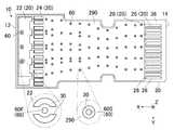
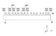
図1及び図4から理解されるように、本発明の実施の形態によるプリント配線板10は、電気信号を中継する中継基板として使用可能である。より具体的には、プリント配線板10は、前後方向(X方向)における前端12に取り付けられた様々なケーブルと、後端14に接続された接続対象物(図示せず)とを中継する中継基板である。接続対象物は、例えばコネクタであってもよいし、ケーブルであってもよい。また、プリント配線板10は、コネクタ内部の中継基板であってもよい。 As can be understood from FIGS. 1 and 4, the printed
図1、図3及び図5を参照すると、プリント配線板10は、上下方向(Z方向)に積層されたパターン層20と絶縁層30とグランド層40とを備えている。詳しくは、絶縁層30は、Z方向と直交する上面36及び下面38を有している。上面36にはパターン層20が形成されており、下面38には、グランド層40が形成されている。換言すれば、絶縁層30は、パターン層20とグランド層40との間に設けられている。 Referring to FIGS. 1, 3, and 5, the printed
本実施の形態において、絶縁層30は、樹脂等の絶縁体から形成されており、パターン層20及びグランド層40の夫々は、銅箔等の導電体からなる様々な導体パターンから構成されている。また、プリント配線板10には、プリント配線板10をZ方向に貫通する複数のビア60が形成されている。ビア60の夫々は、パターン層20の導体パターンとグランド層40の導体パターンとを電気的に互いに接続している。 In the present embodiment, the insulating
図3に示されるように、グランド層40には、導体パターンとして、グランドパターン42が形成されている。本実施の形態によれば、グランドパターン42は下面38の殆どを覆っており、グランド層40は、グランドパターン42以外の導体パターンを有していない。しかしながら、グランド層40には、グランドパターン42以外の導体パターン等が形成されていてもよい。 As shown in FIG. 3, a
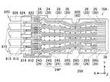
図1及び図2に示されるように、パターン層20には、導体パターンとして、1つの共通グランド22と、複数のパッド24と、複数の接続部26と、複数の連結パターン28とが形成されている。連結パターン28の殆どは、絶縁体からなるレジスト290によって覆われている。パターン層20には、その他の導体パターン等が形成されていてもよい。 As shown in FIGS. 1 and 2, the
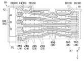
図2に示されるように、共通グランド22は、プリント配線板10の前端12近傍に位置しており、横方向(Y方向)に沿って延びている。共通グランド22は、X方向においてパッド24の前方(前端12側)に位置している。パッド24は、横方向(Y方向)に並んでいる。本実施の形態において、パッド24は、+Y側の2つのパッド24を除き、共通グランド22と僅かな距離をあけて、共通グランド22の真後ろに位置している。 As shown in FIG. 2, the
接続部26は、プリント配線板10の後端14近傍に位置しており、Y方向に並んでいる。接続部26は、パッド24と夫々対応している。より具体的には、接続部26は、連結パターン28によってパッド24と夫々接続されている。換言すれば、連結パターン28は、パッド24と接続部26とを連結している。 The
図2及び図4に示されるように、パッド24は、1以上のグランドパッド24Gと、1以上の信号パッド24Sとを含んでいる。詳しくは、本実施の形態においては、グランドパッド24Gの数は5であり、信号パッド24Sの数は10である。グランドパッド24Gは、共通グランド22と接続されており、信号パッド24Sは、共通グランド22と接続されていない。換言すれば、パッド24のうち共通グランド22と接続されたものがグランドパッド24Gである。 As shown in FIGS. 2 and 4, the
本実施の形態によるパッド24は、2つの信号パッド24Sから夫々構成される4つの(即ち、複数の)信号パッド対24Pと、信号パッド対24Pを構成しない2つの信号パッド24Sを含んでいる。後述するように、信号パッド対24Pは、差分信号(差動信号)を伝送する際に使用される。信号パッド対24Pを構成しない信号パッド24Sは、プリント配線板10の+Y側の側部に位置している。 The
パッド24は、信号パッド対24Pよりも1つだけ多いグランドパッド24Gを含んでいる。グランドパッド24Gと信号パッド対24Pとは、Y方向において交互に並んでいる。換言すれば、信号パッド対24Pは、Y方向において2つのグランドパッド24Gの間に挟まれている。信号パッド対24Pを挟むグランドパッド24Gの間には、信号パッド対24P以外の導体パターンが設けられていない。 The
図2に示されるように、接続部26は、パッド24と同様に、5つのグランド接続部26Gと、10の信号接続部26Sとを含んでいる。同様に、連結パターン28は、5つのグランド連結パターン28Gと、10の信号連結パターン28Sとを含んでいる。グランド連結パターン28Gは、グランドパッド24Gをグランド接続部26Gと夫々連結しており、信号連結パターン28Sは、信号パッド24Sを信号接続部26Sと夫々連結している。換言すれば、接続部26のうちグランドパッド24Gに連結されたものがグランド接続部26Gであり、信号パッド24Sに連結されたものが信号接続部26Sである。 As shown in FIG. 2, the
本実施の形態によれば、グランドパッド24G及び信号パッド24Sは、互いに同一な形状及びサイズを有している。グランド接続部26G及び信号接続部26Sも、互いに同じ形状及びサイズを有しており、Y方向に等間隔に並べられている。一方、グランド連結パターン28Gの幅(Y方向におけるサイズ)は、信号連結パターン28Sの幅よりも大きい。但し、本発明はこれに限定されない。例えば、グランドパッド24Gは、信号パッド24Sと異なった形状やサイズを有していてもよい。 According to the present embodiment, the
図1乃至図3を参照すると、本実施の形態によるビア60は、3つの第1ビア(以下「ビア」という。)60Fと、複数の第2ビア(以下「ビア」という。)60Sとを含んでいる。パターン層20において、ビア60Fは共通グランド22に設けられており、ビア60Sはグランド連結パターン28Gに設けられている。このため、共通グランド22は、ビア60のうちの少なくとも1つのビア60Fによってグランド層40のグランドパターン42と電気的に接続されており、グランド連結パターン28Gの夫々は、ビア60のうちの少なくとも1つのビア60Sによってグランドパターン42と電気的に接続されている。換言すれば、ビア60のうち共通グランド22に設けられたものがビア60Fであり、グランド連結パターン28Gに設けられたものがビア60Sである。 Referring to FIGS. 1 to 3, a via 60 according to the present embodiment includes three first vias (hereinafter referred to as “vias”) 60F and a plurality of second vias (hereinafter referred to as “vias”) 60S. Contains. In the
本実施の形態によれば、ビア60F及びビア60Sは、互いに同じ形状及びサイズを有している。ビア60Fの周囲にはサーマルランドが形成されている。但し、本発明はこれに限定されない。例えば、ビア60Fとビア60Sのサイズは異なっていてもよい。 According to the present embodiment, the via 60F and the via 60S have the same shape and size. A thermal land is formed around the via 60F. However, the present invention is not limited to this. For example, the size of the via 60F and the via 60S may be different.
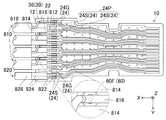
図4及び図5に示されるように、プリント配線板10は、使用時に様々なケーブルと接続される。本実施の形態においては、4つのツインナックスケーブル(ケーブル)810と1つのツイストペアケーブル(ケーブル)820が、プリント配線板10の上面36に取り付けられる。詳しくは、ケーブル810の絶縁体814及びケーブル820の絶縁体824は、共通グランド22又はプリント配線板10の上面36に、位置決めされて接着剤等によって固定される。絶縁体814及び絶縁体824は、コネクタ(図示せず)やコネクタを覆うフード(図示せず)等の固定手段によって、位置決めして固定しても良い。 As shown in FIGS. 4 and 5, the printed
図4に示されるように、ケーブル810の夫々は、2つの信号導体812と、信号導体812を夫々覆う2つの絶縁体814と、絶縁体814の外部に設けられたドレイン線816と、絶縁体814及びドレイン線816を覆う被覆818とを備えている。絶縁体814及び被覆818は、ケーブル810の先端部(−X側の端部)において剥がされており、信号導体812及びドレイン線816が外部に露出している。信号導体812は、信号パッド対24Pの信号パッド24Sに、半田付け等によって夫々接続されて固定され、ドレイン線816は、半田付け等によってグランドパッド24Gに接続されて固定される。 As shown in FIG. 4, each of the
ケーブル820は、2つの信号導体822と、信号導体822を夫々覆う2つの絶縁体824と、絶縁体824を覆う被覆828とを備えている。被覆828は、ケーブル820の先端部において剥がされており、信号導体822が外部に露出している。信号導体822は、信号パッド対24Pを構成していない信号パッド24Sに、半田付け等によって夫々接続されて固定される。 The
図4を参照すると、ケーブル810の先端部(露出部)は、信号導体822がグランド電位を有する部位で覆われていないため、ケーブル810の先端部以外の部位よりも大きなインピーダンスを有する。しかしながら、本実施の形態によれば、共通グランド22、グランドパッド24G及びグランドパターン42(図3参照)は、互いに接続されてグランド電位を有する。また、ケーブル810の露出部は、共通グランド22上に配置される。このため、ケーブル810のインピーダンスが整合し、ケーブル810を使用して高周波信号を伝送する場合でも信号特性が劣化し難い。 Referring to FIG. 4, the tip portion (exposed portion) of
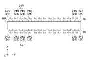
更に、図6を参照すると、Y方向において隣り合う2つの信号パッド対24Pは、グランドパッド24Gによって隔てられている。このため、ケーブル810が例えば差分信号(差動信号)を伝送する場合、一方の信号パッド対24Pの信号パッド24Sと、他方の信号パッド対24Pの信号パッド24Sとの間のクロストークが防止される。換言すれば、プリント配線板10の上面36に沿った信号パッド24S間のクロストークが防止できる。特に、本実施の形態によれば、クロストークを防止するための特別な部材を必要としない。このため、信号パッド24S間のピッチ幅を小さくできる。即ち、実施の形態によるプリント配線板10は、小型化に適している。 Further, referring to FIG. 6, two signal pad pairs 24P adjacent in the Y direction are separated by a
図2に示されるように、本実施の形態によれば、グランドパッド24Gは、短い導体パターンによって共通グランド22と直接的に接続されている。換言すれば、グランドパッド24Gは、パターン層20において共通グランド22と接続されている。グランドパッド24Gは、グランド層40(図3参照)において共通グランド22と接続されていてもよい。例えば、グランドパッド24Gにビア60を形成してもよい。但し、グランド電位をより安定させてインピーダンスの整合及びクロストークの防止といった効果をより確実に得るという観点からは、本実施の形態のように構成することが好ましい。 As shown in FIG. 2, according to the present embodiment, the
図2及び図3を参照すると、グランド層40のグランドパターン42は、信号パッド24Sに接続された信号連結パターン28Sの直下に少なくとも形成されている。即ち、信号連結パターン28Sは、マイクロストリップラインを構成している。マイクロストリップラインを構成するためには、グランドパターン42は信号連結パターン28Sの直下のみに形成されていればよい。但し、グランド電位をより安定させるという観点からは、グランドパターン42は、本実施の形態のようにベタパターンであるほうが好ましい。 2 and 3, the
図2から理解されるように、ビア60Fは、共通グランド22のX方向における中間線CLよりも(即ち、X方向における中間点よりも)前方に位置している。換言すれば、ビア60Fは、X方向において可能な限り前端12近くに位置するように形成されている。また、ビア60Fは、共通グランド22のY方向における中間部だけでなく、両側部にも夫々形成されている。このため、グランド電位をより安定させることができる。 As understood from FIG. 2, the via 60 </ b> F is located in front of the intermediate line CL in the X direction of the common ground 22 (that is, from the intermediate point in the X direction). In other words, the via 60F is formed as close to the
図3及び図4を参照すると、本実施の形態によれば、グランドパッド24Gに接続されたグランド連結パターン28Gの夫々は、複数のビア60Sによってグランドパターン42に接続されている。ビア60Sは、少なくともグランド連結パターン28GのX方向における両端部に夫々設けられている。このため、グランド電位を更に安定させることができる。また、ビア60Sは、グランド連結パターン28Gに沿って小さな間隔をあけて並んでいる。ビア60Sの間の間隔を、ケーブル810が伝達する信号の波長によって規定される所定値よりも小さく設定することで、グランドパターン42における共振を防止できる。 3 and 4, according to the present embodiment, each of the
図2及び図4に示されるように、ビア60Fは、Y方向において信号パッド24Sと異なる位置にある。このため、ケーブル810の絶縁体814を、ビア60Fに邪魔されることなく共通グランド22上に安定的に置くことができる。 As shown in FIGS. 2 and 4, the via 60F is located at a position different from the
本実施の形態によるプリント配線板10は、既に述べた変形例に加えて、以下に説明するように様々に変形可能である。 The printed
図2を参照すると、パターン層20には、信号パッド対24Pを挟むグランドパッド24Gに加えて、その他のグランドパッド24Gが形成されていてもよい。また、信号パッド対24Pの数は1であってもよい。即ち、パッド24は、信号パッド対24Pを少なくとも1つ含んでおり、且つ、信号パッド対24Pよりも多数のグランドパッド24Gを含んでいればよい。 Referring to FIG. 2, the
図2及び図3から理解されるように、1つのビア60Fのみによって、共通グランド22、グランドパッド24G及びグランドパターン42を、互いに電気的に接続できる。従って、プリント配線板10には、1以上のビア60が形成されていればよい。但し、グランド電位を安定させるという観点からは、本実施のように構成することが好ましい。 As can be understood from FIGS. 2 and 3, the
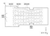
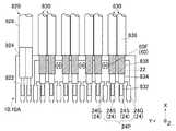
本発明は、図7乃至図10に示されるように、プリント配線板10(図1参照)と少し異なるプリント配線板10Aにも適用可能である。プリント配線板10Aは、全体としてプリント配線板10とプリント配線板10の鏡像とを上下に貼り合わせたような構造を有している。プリント配線板10Aの各層の構造は、プリント配線板10と基本的に同じであり、プリント配線板10と同様な効果を発揮する。以下、プリント配線板10Aの構造のうちプリント配線板10との相違点を中心に説明する。 The present invention can be applied to a printed
図8に示されるように、プリント配線板10Aは、パターン層20、絶縁層30及びグランド層40からなるセットを2セット備えており、且つ、中間絶縁層50を備えている。この2つのセットは、中間絶縁層50を間に挟んでZ方向に積層されている。上側(+Z側)のセットにおいては、パターン層20は上面36に位置しており、グランド層40は下面38に位置している。下側(−Z側)のセットにおいては、パターン層20は下面38に位置しており、グランド層40は上面36に位置している。即ち、中間絶縁層50は、2つのセットのグランド層40の間に設けられている。 As shown in FIG. 8, the printed
図8を図1と合わせて参照すると、プリント配線板10Aの上側のセットのパターン層20は、プリント配線板10のパターン層20と同一の構造を有しており、レジスト290によって覆われている。図7を図1と合わせて参照すると、プリント配線板10Aの下側のセットのパターン層20は、プリント配線板10のパターン層20のXY平面に関する鏡像であり、レジスト290によって覆われている。換言すれば、一方のセット(上側のセット)のパターン層20に形成された共通グランド22、パッド24、接続部26及び連結パターン28は、X方向及びY方向の双方において、他方のセット(下側のセット)のパターン層20に形成された共通グランド22、パッド24、接続部26及び連結パターン28と夫々同じ位置にある。 Referring to FIG. 8 together with FIG. 1, the
同様に、図8を図3と合わせて参照すると、プリント配線板10Aの上側のセットのグランド層40は、プリント配線板10のグランド層40と同一の構造を有しており、プリント配線板10Aの下側のセットのグランド層40は、プリント配線板10のグランド層40のXY平面に関する鏡像である。換言すれば、一方のセット(上側のセット)のグランド層40に形成されたグランドパターン42は、X方向及びY方向の双方において、他方のセット(下側のセット)のグランド層40に形成されたグランドパターン42と同じ位置にある。 Similarly, referring to FIG. 8 together with FIG. 3, the
図7を参照すると、プリント配線板10Aは、上述の鏡対称構造を有しているため、ビア60の夫々をZ方向に貫通させることができる。即ち、プリント配線板10Aは、製造し易い構造を有している。 Referring to FIG. 7, the printed
図7乃至図9から理解されるように、プリント配線板10Aの上面36及び下面38の夫々のパッド24は、プリント配線板10の上面36(図4参照)と同様に、使用時においてケーブル810及びケーブル820と接続される。このため、図10に示されるように、上面36及び下面38の夫々において、プリント配線板10の上面36(図6参照)と同様に、信号パッド対24Pを、Y方向においてグランド電位(グランドパッド24G)で挟むことができる。 7 to 9, the
図11に示されるように、プリント配線板10やプリント配線板10Aには、ケーブル810に代えて同軸ケーブル(ケーブル)830を取り付けることができる。ケーブル830の夫々は、信号導体832と、信号導体832を覆う絶縁体834と、絶縁体834を覆うグランド導体836と、グランド導体836を覆う被覆838とを備えている。絶縁体834及び被覆838は、ケーブル830の先端部において剥がされており、信号導体832及びグランド導体836が外部に露出している。 As shown in FIG. 11, a coaxial cable (cable) 830 can be attached to the printed
図4及び図11を参照すると、1つのケーブル810に代えて一対のケーブル830によって差分信号(差動信号)を伝送することができる。この場合、信号導体832は、信号パッド対24Pの信号パッド24Sに、半田付け等によって接続されて固定され、グランド導体836は、半田付け等によって共通グランド22に接続されて固定される。この場合にも、図6及び図10に示されるように、信号パッド対24Pを、Y方向においてグランド電位(グランドパッド24G)で挟むことができる。 Referring to FIGS. 4 and 11, a differential signal (differential signal) can be transmitted by a pair of
本実施の形態によるプリント配線板10は、以下に説明するように、差分信号(差動信号)を中継しない中継基板にも適用可能である。 The printed
図12を参照すると、プリント配線板10Bは、プリント配線板10(図1参照)やプリント配線板10A(図7参照)のパターン層20と少し異なるパターン層20Bを備えていることを除き、プリント配線板10やプリント配線板10Aと同様に構成されている。 Referring to FIG. 12, the printed
パターン層20Bは、パターン層20(図2参照)と同様な共通グランド22を有しており、且つ、パターン層20のパッド24(図2参照)と同一形状及びサイズのパッド24を有している。但し、パターン層20Bのパッド24の配置は、パターン層20と異なっている。より具体的には、パターン層20Bのパッド24は、6つの(即ち、1以上の)信号パッド24Sと、7つの(即ち、1以上の)グランドパッド24Gを含んでいる。換言すれば、パッド24は、信号パッド24Sよりも1つだけ多いグランドパッド24Gを含んでいる。信号パッド24Sとグランドパッド24Gとは、Y方向において交互に並んでいる。 The
プリント配線板10Bの使用時に、例えばケーブル830(図11参照)の信号導体832が信号パッド24Sに接続され、グランド導体836が共通グランド22に接続される。ケーブル830をこのように接続することで、例えば、ケーブル830が高周波数のアナログ信号を伝送する際、ケーブル830のインピーダンスを整合させると共に、信号パッド24S間のクロストークを防止できる。 When the printed
パターン層20Bは、様々に変形可能である。例えば、信号パッド24Sのうちの幾つかをグランドパッド24Gによって挟む必要がない場合、グランドパッド24Gの数は信号パッド24Sの数よりも少なくてもよい。但し、この場合も、パッド24は、複数のグランドパッド24Gを含んでいる。また、信号パッド24Sのうちの少なくとも1つは、Y方向において2つのグランドパッド24Gの間に挟まれている。 The
図2及び図12を参照すると、パターン層20及びパターン層20Bは、組み合わせてもよい。詳しくは、グランドパッド24Gに挟まれた信号パッド対24Pとグランドパッド24Gに挟まれた単独の信号パッド24Sとが混在していてもよい。 2 and 12, the
10,10A,10B プリント配線板
12 前端
14 後端
20,20B パターン層
22 共通グランド
24 パッド
24G グランドパッド(パッド)
24S 信号パッド(パッド)
24P 信号パッド対
26 接続部
26G グランド接続部(接続部)
26S 信号接続部(接続部)
28 連結パターン
28G グランド連結パターン(連結パターン)
28S 信号連結パターン(連結パターン)
290 レジスト
30 絶縁層
36 上面
38 下面
40 グランド層
42 グランドパターン
50 中間絶縁層
60 ビア
60F 第1ビア(ビア)
60S 第2ビア(ビア)
810 ツインナックスケーブル(ケーブル)
812 信号導体
814 絶縁体
816 ドレイン線
818 被覆
820 ツイストペアケーブル(ケーブル)
822 信号導体
824 絶縁体
828 被覆
830 同軸ケーブル(ケーブル)
832 信号導体
834 絶縁体
836 グランド導体
838 被覆
X 前後方向
Y 横方向
Z 上下方向10, 10A, 10B Printed
24S Signal pad (pad)
24P
26S signal connection (connection)
28
28S signal connection pattern (connection pattern)
290 resist 30 insulating
60S 2nd via (via)
810 Twinax cable (cable)
812
832
Claims (11)
Translated fromJapanese前記絶縁層は、前記パターン層と前記グランド層との間に設けられており、
前記グランド層には、グランドパターンが形成されており、
前記パターン層には、1つの共通グランドと、前記上下方向と直交する横方向に並ぶ複数のパッドとが形成されており、
前記共通グランドは、前記上下方向及び前記横方向の双方と直交する前後方向において前記パッドの前方に位置しており、且つ、前記ビアのうちの少なくとも1つによって前記グランド層の前記グランドパターンと接続されており、
前記パッドは、1以上のグランドパッドと1以上の信号パッドとを含んでおり、前記グランドパッドの全てが前記共通グランドと直接的に接続されており、前記信号パッドは前記共通グランドと接続されておらず、
前記プリント配線板は、前記前後方向において前端と後端とを有しており、
前記パッドは、前記前後方向において前記後端よりも前記前端に近い位置に配置されている
プリント配線板。A printed wiring board comprising a pattern layer, an insulating layer, and a ground layer stacked in the vertical direction, and having one or more vias formed thereon,
The insulating layer is provided between the pattern layer and the ground layer,
In the ground layer, a ground pattern is formed,
In the pattern layer, one common ground and a plurality of pads arranged in a lateral direction perpendicular to the vertical direction are formed,
The common ground is located in front of the pad in the front-rear direction orthogonal to both the vertical direction and the horizontal direction, and is connected to the ground pattern of the ground layer by at least one of the vias. Has been
The pad includes one or more ground pads and one or more signal pads, all of the ground padsaredirectly connected to the common ground, and the signal pads are connected to the common ground. Not
The printed wiring board has a front end and a rear end in the front-rear direction,
The pad is a printed wiring board disposed in a position closer to the front end than the rear end in the front-rear direction.
前記パッドは、2つの前記信号パッドからなる信号パッド対を少なくとも1つ含んでおり、且つ、前記信号パッド対よりも多数の前記グランドパッドを含んでおり、
前記信号パッド対は、前記横方向において2つの前記グランドパッドの間に挟まれている
プリント配線板。The printed wiring board according to claim 1,
The pad includes at least one signal pad pair including the two signal pads, and includes a larger number of the ground pads than the signal pad pair.
The signal pad pair is a printed wiring board sandwiched between two ground pads in the lateral direction.
前記パッドは、複数の前記信号パッド対と、前記信号パッド対よりも1つだけ多い前記グランドパッドとを含んでおり、
前記グランドパッドと前記信号パッド対とは、前記横方向において交互に並んでいる
プリント配線板。The printed wiring board according to claim 2,
The pad includes a plurality of the signal pad pairs and the ground pad that is one more than the signal pad pairs,
The printed wiring board in which the ground pads and the signal pad pairs are alternately arranged in the lateral direction.
前記パッドは、複数の前記グランドパッドを含んでおり、
前記信号パッドのうちの少なくとも1つは、前記横方向において2つの前記グランドパッドの間に挟まれている
プリント配線板。The printed wiring board according to claim 1,
The pad includes a plurality of the ground pads,
At least one of the signal pads is a printed wiring board sandwiched between two ground pads in the lateral direction.
前記パッドは、前記信号パッドと、前記信号パッドよりも1つだけ多い前記グランドパッドとを含んでおり、
前記信号パッドと前記グランドパッドとは、前記横方向において交互に並んでいる
プリント配線板。The printed wiring board according to claim 4,
The pad includes the signal pad and the ground pad that is only one more than the signal pad;
The printed wiring board in which the signal pads and the ground pads are alternately arranged in the lateral direction.
前記グランドパッドは、前記パターン層において前記共通グランドと接続されている
プリント配線板。A printed wiring board according to any one of claims 1 to 5,
The ground pad is a printed wiring board connected to the common ground in the pattern layer.
前記共通グランドと前記グランドパターンとを接続する前記ビアは、前記共通グランドの前記前後方向における中間点よりも前方に位置している
プリント配線板。The printed wiring board according to any one of claims 1 to 6,
The via that connects the common ground and the ground pattern is a printed wiring board positioned in front of an intermediate point in the front-rear direction of the common ground.
前記共通グランドと前記グランドパターンとを接続する前記ビアは、前記横方向において前記信号パッドと異なる位置にある
プリント配線板。A printed wiring board according to any one of claims 1 to 7,
The via that connects the common ground and the ground pattern is a printed wiring board at a position different from the signal pad in the lateral direction.
前記パターン層には、前記パッドと夫々対応する複数の接続部と、前記パッドを前記接続部と夫々連結する複数の連結パターンとが形成されており、
前記グランド層の前記グランドパターンは、前記信号パッドに接続された前記連結パターンの直下に少なくとも形成されている
プリント配線板。A printed wiring board according to any one of claims 1 to 8,
In the pattern layer, a plurality of connection portions respectively corresponding to the pads and a plurality of connection patterns for connecting the pads to the connection portions are formed.
The printed wiring board, wherein the ground pattern of the ground layer is formed at least directly below the connection pattern connected to the signal pad.
前記グランドパッドに接続された前記連結パターンは、前記ビアのうちの少なくとも1つによって前記グランド層の前記グランドパターンと接続されている
プリント配線板。The printed wiring board according to claim 9,
The printed circuit board, wherein the connection pattern connected to the ground pad is connected to the ground pattern of the ground layer by at least one of the vias.
前記パターン層、前記絶縁層及び前記グランド層からなるセットを2セット備えており、且つ、中間絶縁層を備えており、
前記中間絶縁層は、2つの前記セットの前記グランド層の間に設けられており、
一方の前記セットの前記パターン層に形成された前記共通グランド、前記パッド、前記接続部及び前記連結パターンは、前記前後方向及び前記横方向の双方において、他方の前記セットの前記パターン層に形成された前記共通グランド、前記パッド、前記接続部及び前記連結パターンと夫々同じ位置にあり、
一方の前記セットの前記グランド層に形成された前記グランドパターンは、前記前後方向及び前記横方向の双方において、他方の前記セットの前記グランド層に形成された前記グランドパターンと同じ位置にある
プリント配線板。The printed wiring board according to claim 9 or 10,
Two sets of the pattern layer, the insulating layer and the ground layer are provided, and an intermediate insulating layer is provided.
The intermediate insulating layer is provided between the ground layers of the two sets;
The common ground, the pad, the connection portion, and the connection pattern formed in the pattern layer of one set are formed in the pattern layer of the other set in both the front-rear direction and the lateral direction. The common ground, the pad, the connecting portion and the connection pattern are in the same position,
The ground pattern formed on the ground layer of one set is in the same position as the ground pattern formed on the ground layer of the other set in both the front-rear direction and the lateral direction. Board.
Priority Applications (4)
| Application Number | Priority Date | Filing Date | Title |
|---|---|---|---|
| JP2014079092AJP5860917B2 (en) | 2014-04-08 | 2014-04-08 | Printed wiring board |
| TW104102976ATWI596995B (en) | 2014-04-08 | 2015-01-29 | Printed wiring board |
| US14/634,597US9572246B2 (en) | 2014-04-08 | 2015-02-27 | Printed wiring board |
| CN201510092231.4ACN104981089B (en) | 2014-04-08 | 2015-03-02 | Printed circuit board (PCB) |
Applications Claiming Priority (1)
| Application Number | Priority Date | Filing Date | Title |
|---|---|---|---|
| JP2014079092AJP5860917B2 (en) | 2014-04-08 | 2014-04-08 | Printed wiring board |
Publications (2)
| Publication Number | Publication Date |
|---|---|
| JP2015201533A JP2015201533A (en) | 2015-11-12 |
| JP5860917B2true JP5860917B2 (en) | 2016-02-16 |
Family
ID=54210998
Family Applications (1)
| Application Number | Title | Priority Date | Filing Date |
|---|---|---|---|
| JP2014079092AActiveJP5860917B2 (en) | 2014-04-08 | 2014-04-08 | Printed wiring board |
Country Status (4)
| Country | Link |
|---|---|
| US (1) | US9572246B2 (en) |
| JP (1) | JP5860917B2 (en) |
| CN (1) | CN104981089B (en) |
| TW (1) | TWI596995B (en) |
Families Citing this family (13)
| Publication number | Priority date | Publication date | Assignee | Title |
|---|---|---|---|---|
| CN105097758B (en)* | 2014-05-05 | 2018-10-26 | 日月光半导体制造股份有限公司 | Substrate, its semiconductor package and its manufacturing method |
| US20170105288A1 (en)* | 2015-10-09 | 2017-04-13 | Tyco Electronics Corporation | Wire alignment process and device |
| CN105896145B (en)* | 2016-05-27 | 2018-05-08 | 深圳市深台帏翔电子有限公司 | Connector |
| US10687422B2 (en)* | 2016-12-16 | 2020-06-16 | Google Llc | Dual-sided FPC assembly and related systems and methods for hotbar soldering FPC assemblies |
| JP7061459B2 (en)* | 2017-12-25 | 2022-04-28 | 日本航空電子工業株式会社 | Circuit board, connector assembly and cable harness |
| US10826243B2 (en)* | 2018-08-28 | 2020-11-03 | Sure-Fire Electrical Corporation | Electric connector terminal configuration structure |
| JP6734911B2 (en)* | 2018-12-04 | 2020-08-05 | 日本航空電子工業株式会社 | Circuit board and cable harness including the same |
| US11844174B2 (en)* | 2019-08-09 | 2023-12-12 | Panasonic Intellectual Property Management Co., Ltd. | Electronic substrate |
| CN110600924A (en)* | 2019-09-30 | 2019-12-20 | 广州视源电子科技股份有限公司 | Connector, electronic equipment and open pluggable OPS equipment |
| JP7701254B2 (en)* | 2021-12-09 | 2025-07-01 | 日本航空電子工業株式会社 | Connectors and harnesses |
| JP2023107606A (en)* | 2022-01-24 | 2023-08-03 | 日本航空電子工業株式会社 | Connector/Cable |
| CN115173103B (en)* | 2022-06-08 | 2025-07-18 | 昆山国显光电有限公司 | Clamping device for connector, circuit board and circuit board connecting assembly |
| CN115996515B (en)* | 2023-03-21 | 2023-07-11 | 之江实验室 | Circuit board and adapter |
Family Cites Families (20)
| Publication number | Priority date | Publication date | Assignee | Title |
|---|---|---|---|---|
| US4871319A (en)* | 1988-12-21 | 1989-10-03 | Amp Incorporated | Molded circuit board for ribbon cable connector |
| US5741729A (en)* | 1994-07-11 | 1998-04-21 | Sun Microsystems, Inc. | Ball grid array package for an integrated circuit |
| US6730860B2 (en)* | 2001-09-13 | 2004-05-04 | Intel Corporation | Electronic assembly and a method of constructing an electronic assembly |
| US6808419B1 (en)* | 2003-08-29 | 2004-10-26 | Hon Hai Precision Ind. Co., Ltd. | Electrical connector having enhanced electrical performance |
| JP4421427B2 (en)* | 2004-08-31 | 2010-02-24 | 富士通コンポーネント株式会社 | Cable connector for balanced transmission |
| JP2007019232A (en) | 2005-07-07 | 2007-01-25 | Fujitsu Ltd | End structure of coaxial cable |
| JP4774920B2 (en)* | 2005-10-31 | 2011-09-21 | ソニー株式会社 | Optical transceiver |
| JP2007234258A (en) | 2006-02-27 | 2007-09-13 | Fujitsu Ltd | Printed circuit board unit |
| US7520757B2 (en)* | 2006-08-11 | 2009-04-21 | Tyco Electronics Corporation | Circuit board having configurable ground link and with coplanar circuit and ground traces |
| JP2008218225A (en) | 2007-03-05 | 2008-09-18 | Fujitsu Ltd | Electronic equipment |
| JP4998741B2 (en) | 2008-03-11 | 2012-08-15 | 住友電気工業株式会社 | Adapter structure, high-frequency cable body and wiring board connector |
| JP5060385B2 (en)* | 2008-05-09 | 2012-10-31 | 富士通コンポーネント株式会社 | Balanced transmission connector and balanced transmission cable connector |
| JP5580994B2 (en)* | 2009-02-20 | 2014-08-27 | 日本オクラロ株式会社 | Optical module |
| JP2010251554A (en)* | 2009-04-16 | 2010-11-04 | Fujikura Ltd | Printed circuit boards and harnesses |
| JP5365389B2 (en) | 2009-07-21 | 2013-12-11 | 住友電気工業株式会社 | Coaxial cable harness |
| JP5353634B2 (en) | 2009-10-27 | 2013-11-27 | 住友電気工業株式会社 | Coaxial cable harness |
| JP2011096574A (en) | 2009-10-30 | 2011-05-12 | Hitachi Cable Ltd | Cable for differential signal transmission |
| JP2012064338A (en) | 2010-09-14 | 2012-03-29 | Fujitsu Ltd | Terminal structure of coaxial cable, connector and board unit |
| JP2012129271A (en)* | 2010-12-14 | 2012-07-05 | Nec Corp | Noise suppression structure |
| US20130264107A1 (en)* | 2012-04-05 | 2013-10-10 | Tyco Electronics Corporation | Circuit board and wire assembly |
- 2014
- 2014-04-08JPJP2014079092Apatent/JP5860917B2/enactiveActive
- 2015
- 2015-01-29TWTW104102976Apatent/TWI596995B/enactive
- 2015-02-27USUS14/634,597patent/US9572246B2/enactiveActive
- 2015-03-02CNCN201510092231.4Apatent/CN104981089B/enactiveActive
Also Published As
| Publication number | Publication date |
|---|---|
| TW201540139A (en) | 2015-10-16 |
| US9572246B2 (en) | 2017-02-14 |
| TWI596995B (en) | 2017-08-21 |
| CN104981089B (en) | 2017-10-27 |
| CN104981089A (en) | 2015-10-14 |
| US20150289362A1 (en) | 2015-10-08 |
| JP2015201533A (en) | 2015-11-12 |
Similar Documents
| Publication | Publication Date | Title |
|---|---|---|
| JP5860917B2 (en) | Printed wiring board | |
| TWI453768B (en) | Composite flexible circuit cable | |
| TWI503848B (en) | Differential mode signal transmission module | |
| CN102801053B (en) | Communication connector and electronic equipment using same | |
| WO2011010621A1 (en) | Coaxial-cable harness | |
| TW201349958A (en) | Circuit board and wire assembly | |
| JP2012064338A (en) | Terminal structure of coaxial cable, connector and board unit | |
| WO2010082593A1 (en) | Connector and cable assembly | |
| TW201324548A (en) | Flexible flat cable | |
| TW202123558A (en) | Connecting object, connector and harness | |
| JP7387412B2 (en) | connector assembly | |
| WO2020261790A1 (en) | Signal transmission circuit and electronic control device | |
| JP2011028903A (en) | Connector with cable and method of manufacturing the same | |
| JP4470935B2 (en) | Multi-core coaxial cable and manufacturing method thereof | |
| CN204230493U (en) | The flat cable of link and band link | |
| JP7060171B2 (en) | Transmission line and circuit board | |
| JP5580144B2 (en) | Cable connector assembly | |
| CN109688698B (en) | Circuit board and electric connector with same | |
| JP2017513203A (en) | Wiring member | |
| US10827603B2 (en) | Printed circuit substrate | |
| JP2010182576A (en) | Flat cable with shield | |
| JP2017199879A (en) | Wiring board | |
| JP2009218085A (en) | Adapter structure, high-frequency cable body, and wiring plate connector | |
| WO2018163315A1 (en) | Base board module | |
| CN112703593A (en) | Wiring board |
Legal Events
| Date | Code | Title | Description |
|---|---|---|---|
| TRDD | Decision of grant or rejection written | ||
| A01 | Written decision to grant a patent or to grant a registration (utility model) | Free format text:JAPANESE INTERMEDIATE CODE: A01 Effective date:20151209 | |
| A61 | First payment of annual fees (during grant procedure) | Free format text:JAPANESE INTERMEDIATE CODE: A61 Effective date:20151221 | |
| R150 | Certificate of patent or registration of utility model | Ref document number:5860917 Country of ref document:JP Free format text:JAPANESE INTERMEDIATE CODE: R150 | |
| R250 | Receipt of annual fees | Free format text:JAPANESE INTERMEDIATE CODE: R250 | |
| R250 | Receipt of annual fees | Free format text:JAPANESE INTERMEDIATE CODE: R250 | |
| R250 | Receipt of annual fees | Free format text:JAPANESE INTERMEDIATE CODE: R250 | |
| R250 | Receipt of annual fees | Free format text:JAPANESE INTERMEDIATE CODE: R250 | |
| R250 | Receipt of annual fees | Free format text:JAPANESE INTERMEDIATE CODE: R250 | |
| R250 | Receipt of annual fees | Free format text:JAPANESE INTERMEDIATE CODE: R250 | |
| R250 | Receipt of annual fees | Free format text:JAPANESE INTERMEDIATE CODE: R250 |