JP5852541B2 - Magnetic bias structure for magnetoresistive sensors - Google Patents
Magnetic bias structure for magnetoresistive sensorsDownload PDFInfo
- Publication number
- JP5852541B2 JP5852541B2JP2012224695AJP2012224695AJP5852541B2JP 5852541 B2JP5852541 B2JP 5852541B2JP 2012224695 AJP2012224695 AJP 2012224695AJP 2012224695 AJP2012224695 AJP 2012224695AJP 5852541 B2JP5852541 B2JP 5852541B2
- Authority
- JP
- Japan
- Prior art keywords
- magnetic
- sensor
- lower layer
- layer
- stack
- Prior art date
- Legal status (The legal status is an assumption and is not a legal conclusion. Google has not performed a legal analysis and makes no representation as to the accuracy of the status listed.)
- Active
Links
- 230000005291magnetic effectEffects0.000titleclaimsdescription136
- 239000000463materialSubstances0.000claimsdescription19
- 230000005415magnetizationEffects0.000claimsdescription18
- 241000849798NitaSpecies0.000claimsdescription13
- 22991000114941xx steelInorganic materials0.000claimsdescription11
- 239000000696magnetic materialSubstances0.000claimsdescription11
- 229910001030Iron–nickel alloyInorganic materials0.000claimsdescription10
- 239000000725suspensionSubstances0.000claimsdescription9
- 229910019222CoCrPtInorganic materials0.000claimsdescription7
- 229910045601alloyInorganic materials0.000claimsdescription6
- 239000000956alloySubstances0.000claimsdescription6
- 229910018979CoPtInorganic materials0.000claimsdescription5
- 239000010410layerSubstances0.000description151
- 238000004519manufacturing processMethods0.000description21
- 238000010586diagramMethods0.000description14
- 238000000034methodMethods0.000description12
- 230000005389magnetismEffects0.000description6
- 230000008878couplingEffects0.000description5
- 238000010168coupling processMethods0.000description5
- 238000005859coupling reactionMethods0.000description5
- 238000003860storageMethods0.000description5
- 230000005330Barkhausen effectEffects0.000description3
- 125000006850spacer groupChemical group0.000description3
- 239000000126substanceSubstances0.000description3
- 241001061076Melanonus zugmayeriSpecies0.000description2
- PNEYBMLMFCGWSK-UHFFFAOYSA-Naluminium oxideInorganic materials[O-2].[O-2].[O-2].[Al+3].[Al+3]PNEYBMLMFCGWSK-UHFFFAOYSA-N0.000description2
- 239000002885antiferromagnetic materialSubstances0.000description2
- 230000004888barrier functionEffects0.000description2
- 230000008859changeEffects0.000description2
- 230000005294ferromagnetic effectEffects0.000description2
- 238000005498polishingMethods0.000description2
- 239000011241protective layerSubstances0.000description2
- 230000004044responseEffects0.000description2
- 229910018072Al 2 O 3Inorganic materials0.000description1
- OKTJSMMVPCPJKN-UHFFFAOYSA-NCarbonChemical compound[C]OKTJSMMVPCPJKN-UHFFFAOYSA-N0.000description1
- 229910019041PtMnInorganic materials0.000description1
- 235000013290Sagittaria latifoliaNutrition0.000description1
- 239000006117anti-reflective coatingSubstances0.000description1
- 230000005290antiferromagnetic effectEffects0.000description1
- 238000000429assemblyMethods0.000description1
- 230000000712assemblyEffects0.000description1
- 238000000231atomic layer depositionMethods0.000description1
- 229910052799carbonInorganic materials0.000description1
- 235000015246common arrowheadNutrition0.000description1
- 238000004590computer programMethods0.000description1
- 239000002772conduction electronSubstances0.000description1
- 239000004020conductorSubstances0.000description1
- 238000005137deposition processMethods0.000description1
- 238000001514detection methodMethods0.000description1
- 230000000694effectsEffects0.000description1
- 239000012777electrically insulating materialSubstances0.000description1
- 238000009713electroplatingMethods0.000description1
- 230000004907fluxEffects0.000description1
- 230000001939inductive effectEffects0.000description1
- 238000001020plasma etchingMethods0.000description1
- 230000008569processEffects0.000description1
- 230000001172regenerating effectEffects0.000description1
- 238000000992sputter etchingMethods0.000description1
- 230000008719thickeningEffects0.000description1
- 230000037303wrinklesEffects0.000description1
Images


Classifications
- G—PHYSICS
- G11—INFORMATION STORAGE
- G11B—INFORMATION STORAGE BASED ON RELATIVE MOVEMENT BETWEEN RECORD CARRIER AND TRANSDUCER
- G11B5/00—Recording by magnetisation or demagnetisation of a record carrier; Reproducing by magnetic means; Record carriers therefor
- G11B5/127—Structure or manufacture of heads, e.g. inductive
- G11B5/33—Structure or manufacture of flux-sensitive heads, i.e. for reproduction only; Combination of such heads with means for recording or erasing only
- G11B5/39—Structure or manufacture of flux-sensitive heads, i.e. for reproduction only; Combination of such heads with means for recording or erasing only using magneto-resistive devices or effects
- G11B5/3903—Structure or manufacture of flux-sensitive heads, i.e. for reproduction only; Combination of such heads with means for recording or erasing only using magneto-resistive devices or effects using magnetic thin film layers or their effects, the films being part of integrated structures
- G11B5/3906—Details related to the use of magnetic thin film layers or to their effects
- G11B5/3929—Disposition of magnetic thin films not used for directly coupling magnetic flux from the track to the MR film or for shielding
- G11B5/3932—Magnetic biasing films
- B—PERFORMING OPERATIONS; TRANSPORTING
- B82—NANOTECHNOLOGY
- B82Y—SPECIFIC USES OR APPLICATIONS OF NANOSTRUCTURES; MEASUREMENT OR ANALYSIS OF NANOSTRUCTURES; MANUFACTURE OR TREATMENT OF NANOSTRUCTURES
- B82Y10/00—Nanotechnology for information processing, storage or transmission, e.g. quantum computing or single electron logic
- G—PHYSICS
- G11—INFORMATION STORAGE
- G11B—INFORMATION STORAGE BASED ON RELATIVE MOVEMENT BETWEEN RECORD CARRIER AND TRANSDUCER
- G11B5/00—Recording by magnetisation or demagnetisation of a record carrier; Reproducing by magnetic means; Record carriers therefor
- G11B5/127—Structure or manufacture of heads, e.g. inductive
- G11B5/33—Structure or manufacture of flux-sensitive heads, i.e. for reproduction only; Combination of such heads with means for recording or erasing only
- G11B5/39—Structure or manufacture of flux-sensitive heads, i.e. for reproduction only; Combination of such heads with means for recording or erasing only using magneto-resistive devices or effects
- G11B2005/3996—Structure or manufacture of flux-sensitive heads, i.e. for reproduction only; Combination of such heads with means for recording or erasing only using magneto-resistive devices or effects large or giant magnetoresistive effects [GMR], e.g. as generated in spin-valve [SV] devices
Landscapes
- Engineering & Computer Science (AREA)
- Chemical & Material Sciences (AREA)
- Nanotechnology (AREA)
- Manufacturing & Machinery (AREA)
- Physics & Mathematics (AREA)
- Mathematical Physics (AREA)
- Theoretical Computer Science (AREA)
- Crystallography & Structural Chemistry (AREA)
- Magnetic Heads (AREA)
- Hall/Mr Elements (AREA)
Description
Translated fromJapanese本発明は、磁気データ記録に関し、特に、自由層に対するバイアス磁場を改善し、バルクハウゼンノイズを低減する磁気バイアス構造を有する磁気読み出しヘッドに関する。 The present invention relates to magnetic data recording, and more particularly to a magnetic read head having a magnetic bias structure that improves the bias magnetic field for the free layer and reduces Barkhausen noise.
コンピュータの心臓部は、磁気ディスクドライブと呼ばれるアセンブリである。磁気ディスクドライブは、回転型磁気ディスクと、回転型磁気ディスクの表面に隣接するサスペンションアームによって懸架される読み書きヘッドと、回転ディスク上にある選択した円形トラックの上方に読み書きヘッドを配置するためにサスペンションアームを揺動させるアクチュエータと、を備える。読み書きヘッドは、空気軸受面(ABS)を有するスライダに直結されている。サスペンションアームは、ディスクが回転していないと、スライダを付勢してディスクの表面と接触させるが、ディスクが回転すると、回転ディスクによって空気が渦流される。スライダが空気軸受に乗ると、回転ディスクに磁気インプレッションを書き込み、回転ディスクから磁気インプレッションを読み出すために読み書きヘッドが使用される。読み書きヘッドは、書き込みおよび読み出し機能を実装するために、コンピュータプログラムに従って動作する処理回路に接続されている。 The heart of a computer is an assembly called a magnetic disk drive. The magnetic disk drive includes a rotating magnetic disk, a read / write head suspended by a suspension arm adjacent to the surface of the rotating magnetic disk, and a suspension for placing the read / write head above a selected circular track on the rotating disk. An actuator for swinging the arm. The read / write head is directly connected to a slider having an air bearing surface (ABS). When the disk is not rotating, the suspension arm urges the slider to contact the surface of the disk, but when the disk rotates, air is swirled by the rotating disk. When the slider rides on the air bearing, a read / write head is used to write magnetic impressions to the rotating disk and read magnetic impressions from the rotating disk. The read / write head is connected to a processing circuit that operates according to a computer program in order to implement write and read functions.
書き込みヘッドは、少なくとも1つのコイルと、書き込み極(write pole)と、1つもしくは複数の戻り極(return pole)と、を備えている。電流がコイルを貫流すると、生成された磁界により、磁束が書き込み極を貫流し、その結果、書き込み極の先端から書き込み磁場が放出される。この磁場は十分に強いために、隣接する磁気ディスクの一部分を局所的に磁化し、それによってデータビットを記録する。書き込み磁場はその後、磁気的に柔らかい磁気メディアの下層を通って書き込みヘッドの戻り極に戻る。 The write head includes at least one coil, a write pole, and one or more return poles. When a current flows through the coil, the generated magnetic field causes the magnetic flux to flow through the write pole, and as a result, the write magnetic field is released from the tip of the write pole. This magnetic field is strong enough to locally magnetize a portion of the adjacent magnetic disk, thereby recording data bits. The write magnetic field then returns to the return pole of the write head through the lower layer of magnetically soft magnetic media.
巨大磁気抵抗(GMR)センサーやトンネル接合磁気抵抗(TMR)センサーなどの磁気抵抗センサーを用いて、磁気メディアから磁気信号を読み出すことができる。センサーは、非磁性導電層(センサーがGMRセンサーである場合)か、あるいは第1の強磁性層と第2の強磁性層との間に挟まれた薄型の非磁性電気絶縁障壁層(センサーがTMRセンサーである場合)を備えており、以降、それぞれ固定層(pinned layer)および自由層と言及する。電流が自由層、スペーサ層および固定層の平面に対して垂直に流れるように(平面に対して垂直な電流(CPP)動作モード)、磁気シールドがセンサースタックの上方および下方に位置付けられており、第1および第2の導線としての役割を果たすこともできる。固定層の磁化方向は、空気軸受面(ABS)に対して垂直に固定されており、自由層の磁化方向は、ABSに対して平行だが、外部磁場を受けて自由に回転する。固定層の磁性は、反強磁性層との交換結合によって固定されているのが典型的である。 Magnetic signals can be read from magnetic media using magnetoresistive sensors such as giant magnetoresistive (GMR) sensors and tunnel junction magnetoresistive (TMR) sensors. The sensor can be a non-magnetic conductive layer (if the sensor is a GMR sensor) or a thin non-magnetic electrically insulating barrier layer sandwiched between a first ferromagnetic layer and a second ferromagnetic layer. Hereinafter referred to as a pinned layer and a free layer, respectively. Magnetic shields are positioned above and below the sensor stack so that the current flows perpendicular to the plane of the free layer, spacer layer and fixed layer (current perpendicular to the plane (CPP) mode of operation); It can also serve as the first and second conductors. The magnetization direction of the fixed layer is fixed perpendicular to the air bearing surface (ABS), and the magnetization direction of the free layer is parallel to the ABS, but rotates freely in response to an external magnetic field. The magnetization of the pinned layer is typically pinned by exchange coupling with the antiferromagnetic layer.
固定層および自由層の磁性が互いに平行のときに伝導電子の散乱が最小化され、固定層および自由層の磁性が逆平行のときに散乱が最大化される。読み出しモードでは、スピンバルブセンサーの抵抗が、回転ディスクからの磁場の大きさに対して概ね線形に変化する。検知電流がスピンバルブセンサーを通じて伝導されると、抵抗の変化によって潜在的な変化が生じ、再生信号として検出および処理される。 The scattering of conduction electrons is minimized when the magnetization of the fixed layer and the free layer are parallel to each other, and the scattering is maximized when the magnetizations of the fixed layer and the free layer are antiparallel. In the read mode, the resistance of the spin valve sensor changes approximately linearly with respect to the magnitude of the magnetic field from the rotating disk. As the sense current is conducted through the spin valve sensor, a change in resistance causes a potential change that is detected and processed as a regenerative signal.
データ密度を最大化するために磁気抵抗センサーの小型化がこれまで以上に進むにつれて、自由層を付勢(biasing)することがこれまで以上に困難になる。自由層が小さくなるにつれて、自由層の磁化は生来的に不安定になり、バイアス構造が小さいほど、バイアス磁場は弱くなる。そのため、非常に小さなセンサーで自由層の安定性を維持するのに十分な強度のバイアス磁場を提供できる構造に対するニーズが依然として存在する。 As the miniaturization of magnetoresistive sensors progresses more than ever to maximize data density, it becomes more difficult than ever to bias the free layer. As the free layer becomes smaller, the magnetization of the free layer becomes inherently unstable, and the smaller the bias structure, the weaker the bias field. Thus, there remains a need for structures that can provide a bias field that is strong enough to maintain the stability of the free layer with very small sensors.
本発明は、センサースタックと、センサースタックに隣接して形成されたハード磁気バイアス構造とを備える磁気読み出しセンサーを提供する。磁気バイアス構造は、その少なくとも一部分が別個の島として形成される第1の下層と、第1の下層の上に形成された第2の下層と、第2の下層の上に形成された磁気材料と、を備える。 The present invention provides a magnetic readout sensor comprising a sensor stack and a hard magnetic bias structure formed adjacent to the sensor stack. The magnetic bias structure includes a first lower layer, at least a portion of which is formed as a separate island, a second lower layer formed on the first lower layer, and a magnetic material formed on the second lower layer. And comprising.
第1の下層は、最適なバイアス磁場を提供するための0.25〜0.75nmの厚さを有し得る。第1の下層は、NiTa、CrMo、CoCrPt、Cr、NiFe、またはこれらの材料のうちの少なくとも1つを含有する合金で構成されてよく、NiTaで構成されるのが最も好ましい。第2の下層は、CrMoで構成され得る。磁気材料は、CoPtまたはCoPtCrであり得る。 The first lower layer may have a thickness of 0.25 to 0.75 nm to provide an optimal bias field. The first lower layer may be composed of NiTa, CrMo, CoCrPt, Cr, NiFe, or an alloy containing at least one of these materials, and is most preferably composed of NiTa. The second lower layer can be composed of CrMo. The magnetic material can be CoPt or CoPtCr.
センサースタックおよびバイアス構造は、磁気シールドの上に形成することができる。第1の下層は、完全に別個の材料の島として形成することができる。あるいは、第1の下層は、磁気シールドの上に、磁気シールドと実質的に平行に形成され、かつ連続層として形成されている第1の部分と、別個の島として形成されている、センサースタックに隣接して形成された第2の部分とで構成することができる。 The sensor stack and bias structure can be formed on the magnetic shield. The first lower layer can be formed as an island of completely separate material. Alternatively, a sensor stack in which the first lower layer is formed as a separate island with a first portion formed on the magnetic shield substantially parallel to the magnetic shield and formed as a continuous layer. And a second portion formed adjacent to the first portion.
新たな磁気バイアス構造は、自由層への磁気バイアスを高め、バルクハウゼンノイズを低減する。新たな第1のシード層により、磁性層は、センサースタックに隣接する磁化自由層とでさえも実質的に平行のままである磁気異方性を有する。 The new magnetic bias structure increases the magnetic bias to the free layer and reduces Barkhausen noise. With the new first seed layer, the magnetic layer has a magnetic anisotropy that remains substantially parallel even with the magnetization free layer adjacent to the sensor stack.
本発明のこれらおよび他の特徴ならびに利点は、好適な実施形態に関する以下の詳細な説明を図と併せて読めば明らかであろう。図中において、同様の参照符号は、全体を通じて同様の要素を示す。 These and other features and advantages of the present invention will be apparent from the following detailed description of the preferred embodiments, taken in conjunction with the drawings. In the drawings, like reference numerals designate like elements throughout.
本発明の性質および利点、ならびに好適な使用態様を十分に理解するために、以下の詳細な説明を添付の図面と併せて参照すべきである。これらの図面は、必ずしも原寸に比例していない。 For a full understanding of the nature and advantages of the present invention, as well as the preferred mode of use, reference should be made to the following detailed description taken in conjunction with the accompanying drawings. These drawings are not necessarily drawn to scale.
以下の説明は、本発明を実施するために現時点で意図される最良の実施形態である。この説明は、本発明の一般原理を説明するためになされたものであり、本明細書で請求される発明の概念を制限することを意図するものではない。 The following description is the best embodiment presently contemplated for carrying out the invention. This description is made for the purpose of illustrating the general principles of the invention and is not intended to limit the inventive concepts claimed herein.
ここで図1を参照すると、本発明を具現化するディスクドライブ100が示されている。図1に示すとおり、少なくとも1つの回転型磁気ディスク112がスピンドル114で支持されており、ディスクドライブモーター118によって回転する。各ディスク上の磁気記録は、磁気ディスク112上の同心データトラック(図示せず)の環状パターンという形態である。 Referring now to FIG. 1, a
少なくとも1つのスライダ113が磁気ディスク112の近くに位置付けられており、各スライダ113は、1つもしくは複数の磁気ヘッドアセンブリ121を支持する。磁気ディスクが回転すると、スライダ113がディスク表面122の上方を内外へと放射状に移動して、所望のデータが書き込まれる磁気ディスクの様々なトラックに磁気ヘッドアセンブリ121がアクセスできるようになる。各スライダ113は、サスペンション115によってアクチュエータアーム119に取り付けられている。サスペンション115は、ディスク表面122に対してスライダ113を付勢するわずかなバネ力を提供する。各アクチュエータアーム119は、アクチュエータ手段127に取り付けられている。図1に示すアクチュエータ手段127は、ボイスコイルモーター(VCM)であってもよい。VCMは、一定の磁場内で移動可能なコイルを備え、コイルの移動方向および速度は、コントローラ129によって供給されるモーター電流信号によって制御される。 At least one
ディスク記憶システムの動作中、磁気ディスク112の回転は、スライダ113とディスク表面122との間で、スライダに対して上方への力または揚力を働かせる空気軸受を生成する。この空気軸受は、したがって、通常動作中にサスペンション115のわずかなバネ力とのバランスを保ち、スライダ113を、小さく略一定の間隔でディスク表面から離し、わずかに上の位置で支持する。 During operation of the disk storage system, the rotation of the
ディスク記憶システムの各種構成要素の動作は、アクセス制御信号および内部クロック信号などの制御ユニット129によって生成される制御信号によって制御される。制御ユニット129は、論理制御回路と、記憶手段と、マイクロプロセッサとを備えるのが典型的である。制御ユニット129は、制御信号を生成して、ライン123上の駆動モーター制御信号およびヘッド位置などの各種システム動作を制御し、ライン128上の制御信号を探す。ライン128上の制御信号は、スライダ113をディスク112上にある所望のデータトラックへと最適に動かし、位置付けるための所望の電流プロファイルを提供する。記録チャネル125を経て、読み書きヘッド121との間で書き込みおよび読み出し信号が通信される。 The operation of the various components of the disk storage system is controlled by control signals generated by the
図2を参照すると、スライダ113にある磁気ヘッド121の方向をさらに詳細に見ることができる。図2はスライダ113のABS図であり、確認できるとおり、誘導型書き込みヘッドと読み出しセンサーとを備える磁気ヘッドがスライダの後端(trailing edge)に位置する。典型的な磁気ディスク記憶システムに関する上記説明および図1の添付の具体例は、提示だけを目的とするものである。ディスク記憶システムが多数のディスクおよびアクチュエータを備え得ること、および各アクチュエータがいくつかのスライダを支持し得ることは明らかなはずである。 Referring to FIG. 2, the direction of the
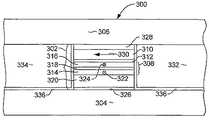
図3は、第1および第2の磁気シールド304、306の間に挟まれているセンサースタック302を有する磁気読み出しヘッド300を示す。磁気シールド304、306は、NiFeなど導電性の磁気材料で構成されており、センサースタック302に検知電流を供給するとともに磁気シールドとしても機能する導線として機能することができる。センサースタック302は、磁化固定層構造308と、磁化自由層310と、それらの間に挟まれた非磁性障壁層またはスペーサ層312とを含むことができる。センサースタック302は、その最下部にシード層326を含んでもよく、シード層326は、上記の堆積層に所望の粒状構造を確実に形成する目的で設けることができる。また、センサースタック302は、製造時に下位層を損傷から保護するために、その最上部にキャップ層328を含んでもよい。キャップ層328は、例えば、RuまたはRu/Ta/Ruであり得る。 FIG. 3 shows a
固定層構造は、Ruなどの非磁性逆平行結合層318をまたがって逆平行結合されている第1および第2の磁性層314、316を備えてもよい。第1の磁性層314は、反強磁性材料の層(AFM層)320によって交換結合することができる。この層は、IrMnまたはPtMnなどの材料で構成され得る。この交換結合は、第1の磁性層314の磁性を、矢印の頭の記号322が示す、ABSに対して垂直な第1の方向に強く固定する。磁性層314、316間の逆方向結合は、矢印の尾の記号324が示す、第1の方向と逆平行であり、かつABSに対して垂直な第2の方向に第2の磁性層316の磁性を固定する。 The fixed layer structure may comprise first and second
自由層310は、矢印330によって示す、ABS図と概ね平行な方向に付勢(bias)される磁性を有する。磁性330はこの方向で付勢されるものの、例えば磁気メディアからの外部磁場に反応して自由に移動する。 The
磁性330の付勢は、ハード磁気バイアス層332、334からのバイアス磁場によって成し遂げられる。これらの磁気バイアス層332、334は、CoPtまたはCoPtCrなどの高保磁力磁気材料から形成される永久磁石である。バイアス層332、334は、アルミナ336、338などの非磁性電気絶縁層の薄層により、センサースタック302から、および少なくとも最下部シールド304から分離される。 The bias of the
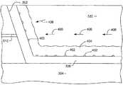
上記のとおり、センサーがこれまで以上に小型化されるにつれて、自由層310の磁性330を付勢することがこれまで以上に困難になる。図4は、本発明の一実施形態にかかる、自由層310に付勢するためにバイアス磁場を増大させるハード磁気バイアス構造の拡大図を示す。図4には1つのバイアス層しか示されていないが、これは一例であり、同様の構造がセンサーの両側に形成できる可能性があることを理解すべきである。 As described above, as the sensor is made smaller than ever, it becomes more difficult than ever to bias the
図4に示すとおり、ハード磁気バイアス層332は、第1および第2の下層402、404の上に形成される。第1の下層402が非常に薄く形成されるのに対し、第2の下層404はそれよりも実質的に厚い。第1の下層402の厚さは低減され、第1の下層が、第2の下層の増厚箇所の核として機能する別個の島から成る構造を有するように、いくつかの原子層になる。つまり、センサースタック302側の第2の下層404で非常に薄い領域が作られるということであり、ハード磁性層332の磁化容易軸(矢印406で明示)は、自由層310と実質的に平行な方向を向いたままである。図4では、センサースタック302の自由層310が例示目的で示されているが、センサースタック302(図3を参照して説明済み)の他の層については、分かりやすくするために省略されている。容易軸の向きが自由層310と概ね平行なので、自由層の付勢を維持するに当たってのバイアス磁場の影響は大きく増大する。 As shown in FIG. 4, the hard
これは、バイアス構造における先行技術と比較することができ、その例が図6に示されている。図6は、標準的な下層602の上に形成されたハード磁気バイアス層604を示す。先行技術による構造では、ハードバイアス層604の磁化容易軸が、矢印606が示す絶縁膜602の経路をたどる。つまり、磁化容易軸606は、自由層310(図3)とはまったく平行ではなく、自由層の平面とほぼ直角である。容易軸のこの向きにより、非常に小さなセンサーサイズにおける自由層の付勢の安定性が実質的に下がり、バルクハウゼンノイズが増大する。 This can be compared with the prior art in bias structure, an example of which is shown in FIG. FIG. 6 shows a hard
図4を再度参照すると、本発明はこの課題を克服し、センサースタック302に隣接する箇所であっても、容易軸406が要望どおり自由層310と平行に整列配置された状態を保つ構造を提供する。第1の下層402は、厚さ0.25nm〜0.75nmであるのが好ましく、NiTa、CrMo、CoCrPt、Cr、NiFeまたはこれらの材料のうちの少なくとも1つを含有する合金のいずれかで構成され得る。第2の下層は、CrMoなどの材料で構成され得る。ハードバイアス層332の材料は、CoPtまたはCoPtCrなどであり得る。 Referring again to FIG. 4, the present invention overcomes this problem and provides a structure that keeps the
図7は、エルステッドで示したハードバイアス磁場と第1のシード層の厚さとの間の関係を示す。図7に示すとおり、第1の下層が厚さ0.25〜0.75へと薄層化されたときに、最大バイアス磁場に達する(データポイント702によって明示)。ただし、第1の下層の厚さがゼロ(すなわち第1の下層が存在しない)まで低減されると、バイアス磁場は大きく低下する(データポイント704によって明示)。そのため、第1の下層402(図4)の厚さは、0.75nmと0.25nmとの間であるのが好ましい。また図4に示すとおり、第1の下層402は、完全な膜ではなく、別個の材料の島として形成されている。 FIG. 7 shows the relationship between the hard bias field shown in Oersted and the thickness of the first seed layer. As shown in FIG. 7, when the first lower layer is thinned to a thickness of 0.25 to 0.75, the maximum bias field is reached (indicated by data point 702). However, when the thickness of the first lower layer is reduced to zero (ie, the first lower layer is not present), the bias magnetic field is greatly reduced (indicated by data point 704). Therefore, the thickness of the first lower layer 402 (FIG. 4) is preferably between 0.75 nm and 0.25 nm. Also, as shown in FIG. 4, the first
ここで図5を参照すると、本発明の代替実施形態では、第1の下層502は、シールド304上方の水平領域に連続層502(a)として形成することができるが、センサースタック302の側面に隣接した垂直に近い領域には、別個の島502(b)として形成される。別個の島構造502(b)がちょうどセンサーの側面に位置することから同様の効果が得られ、異方性504が所望に応じて自由層310と平行の向きを保つのに対し、追加下層502(a)は、上記堆積層404、332で所望の粒成長を促進する必要がある場合に利用できる。 Referring now to FIG. 5, in an alternative embodiment of the present invention, the first
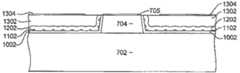
図8〜図16は、本発明の一実施形態にかかる、磁気センサーを製造するための方法を示す。特に図8を参照すると、磁気シールド702が形成されている。磁気シールドは、NiFeなどの材料で構成され得る。その後、一連のセンサー層704がシールドの上に堆積する。センサー層704は、図3を参照しながら先ほど説明したセンサースタック302の層を含み得るが、他の何らかのセンサー構造も可能であり得る。ダイヤモンド状炭素(DLC)など、化学機械研磨に対して耐性のある材料705の層(第1のCMP停止層)が、センサー層704の上に堆積することができる。センサー層704およびCMP停止層705の上には、マスク構造706が形成される。マスクは、リソグラフィーでパターン形成されたレジスト材料を含んでよく、底部反射防止コーティング材(BARC:bottom anti-reflective coating)および/またはハードマスク層および画像転写層など他の材料を含んでもよい。マスク構造706は、センサー幅(トラック幅)を画定するように構成されている幅を有する。 8-16 illustrate a method for manufacturing a magnetic sensor according to one embodiment of the present invention. With particular reference to FIG. 8, a
図9を参照すると、センサー幅を確定するために、マスク構造706によって保護されていないCMP停止層705およびセンサー層704の複数部分を取り除くイオンミリングが実行される。その後、電気絶縁材料の薄層1002が堆積される。絶縁層1002は、アルミナ(Al2O3)であるのが好ましく、原子層堆積法などの共形堆積プロセス(conformal deposition process)によって堆積されるのが好ましい。Referring to FIG. 9, ion milling is performed to remove portions of the
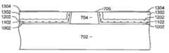
次に図11を参照すると、非常に薄い第1の下層1102が堆積されている。第1の下層は、NiTa、CrMo、CoCrPt、Cr、NiFeであってよく、NiTaであるのが最も好ましい。上記のとおり、第1の下層は、0.25nm〜0.75nmの厚さまで堆積され、図11に示す別個の島を形成するように堆積される。ただし、第1の下層1102は、(図5にて先述のとおり、)シールド702の上の連続層として、かつセンサースタック704の側面で一連の別個の島として堆積できる可能性がある。第1の下層1102が堆積された後、第1の下層1102の表面は、Ar+O2ガスなどで酸化させることができる。Referring now to FIG. 11, a very thin first
図12を参照すると、第2の下層1202が第1の下層1102の上に堆積される。第2の下層は、CrMoで構成され得る。図13を参照すると、次にハード磁気バイアス材料1302の層が堆積され、続いて保護層1304が堆積される。ハード磁気材料1302は、CoPtまたはCoPtCrなどの材料であってよく、保護層は、CrまたはTaなどの材料であってよく、この層は、製造時に下位のハード磁気材料1302を保護することができる。 Referring to FIG. 12, a second
化学機械研磨(CMP)が実行され、図14に示すような構造になる。これが、マスク層706(図13)を取り除くためのしわ焼成(wrinkle bake)および/または化学リフトオフ(chemical liftoff)などの処理を伴ってもよい。その後、残留するCMP停止層705をセンサー層704の最上部から取り除くために反応性イオンエッチングを実行してよく、図15に示すような構造が残る。最後に、図16を参照すると、電気メッキなどにより、NiFeなどの材料から構成される上側磁気シールド1602を形成することができる。 Chemical mechanical polishing (CMP) is performed, resulting in the structure shown in FIG. This may involve processes such as wrinkle bake and / or chemical liftoff to remove mask layer 706 (FIG. 13). Thereafter, reactive ion etching may be performed to remove the remaining
以上、各種実施形態を記載してきたが、それらは例示目的でのみ提示されており、限定目的でないという点は理解すべきである。本発明の範囲内に属する他の実施形態が当業者にとって明らかになることもある。そのため、本発明の幅および範囲は、上記の例示的な実施形態のいずれによっても制限されるべきでなく、以下の請求項とそれらの均等物とに従ってのみ定義されるべきである。 While various embodiments have been described above, it should be understood that they are presented for illustrative purposes only and are not limiting purposes. Other embodiments within the scope of the invention may be apparent to those skilled in the art. As such, the breadth and scope of the present invention should not be limited by any of the above-described exemplary embodiments, but should be defined only in accordance with the following claims and their equivalents.
100 ディスクドライブ
112 磁気ディスク
113 スライダ
114 スピンドル
115 サスペンション
118 ディスクドライブモーター
119 アクチュエータアーム
121 磁気ヘッドアセンブリ
122 ディスク表面
123 ライン
125 記録チャネル
127 アクチュエータ手段
128 ライン
129 制御ユニット
300 磁気読み出しヘッド
302 センサースタック
304 第1の磁気シールド
306 第2の磁気シールド
308 磁化固定層構造
310 磁化自由層
312 スペーサ層
314 第1の磁性層
316 第2の磁性層
318 非磁性逆平行結合層
320 反強磁性材料の層
322 矢印の頭
324 矢印の尾
326 シード層
328 キャップ層
332 ハード磁気バイアス層
334 ハード磁気バイアス層
402 第1の下層
404 第2の下層
406 磁化容易軸
502 第1の下層
502(a) 連続層
502(b) 別個の島
602 下層絶縁膜
604 ハード磁気バイアス層
606 磁化容易軸
702 磁気シールド
704 センサー層
705 第1のCMP停止層
706 マスク層
1002 絶縁層
1102 第1の下層
1202 第2の下層
1302 ハード磁気材料
1602 上側磁気シールドDESCRIPTION OF
Claims (17)
Translated fromJapanese前記センサースタックに隣接して形成されたハード磁気バイアス構造と、
を備え
前記ハード磁気バイアス構造が、第1の下層と、前記第1の下層の上に形成された第2の下層と、前記第2の下層の上に形成された磁気材料とを備え、
前記第1の下層が、磁気シールドの上に形成され、前記磁気シールドと実質的に平行である第1の部分と、前記センサースタックの側面に隣接する第2の部分とを有し、前記第1の下層の前記第1の部分が連続膜として形成され、前記第2の部分が別個の島として形成される、磁気読み出しセンサー。The sensor stack,
A hard magnetic bias structure formed adjacent to the sensor stack;
The hard magnetic bias structure comprising acan, comprising afirst lower and a second lower layer formed on said first layer, and a magnetic material formed over said secondlayer,
The first lower layer includes a first portion formed on the magnetic shield and substantially parallel to the magnetic shield; and a second portion adjacent to a side surface of the sensor stack; A magnetic read sensor, wherein the first portion of the lower layer of 1 is formed as a continuous film and the second portion is formed as a separate island .
前記センサースタックが、前記ハード磁気バイアス構造を、前記センサースタックおよび前記磁気シールドから分離させる電気絶縁層をさらに備える、請求項1に記載の磁気センサー。The magnetic sensor of claim 1, wherein the sensor stack further comprises an electrically insulating layer that separates the hard magnetic bias structure from the sensor stack and the magnetic shield.
磁気メディアと、Magnetic media,
サスペンションアセンブリと、A suspension assembly;
前記サスペンションアセンブリに取り付けられた磁気読み出しヘッドと、A magnetic read head attached to the suspension assembly;
を備え、With
前記磁気読み出しヘッドが、The magnetic read head comprises:
センサースタックと、The sensor stack,
前記センサースタックに隣接して形成されたハード磁気バイアス構造と、A hard magnetic bias structure formed adjacent to the sensor stack;
を備え、With
前記ハード磁気バイアス構造が、第1の下層と、第2の下層の上に形成された磁気材料とを備え、The hard magnetic bias structure comprises a first lower layer and a magnetic material formed on the second lower layer;
前記第1の下層が、磁気シールドの上に形成され、前記磁気シールドと実質的に平行である第1の部分と、前記センサースタックの側面に隣接する第2の部分とを有し、前記第1の下層の前記第1の部分が連続膜として形成され、前記第2の部分が別個の島として形成される、磁気データ記録システム。The first lower layer includes a first portion formed on the magnetic shield and substantially parallel to the magnetic shield; and a second portion adjacent to a side surface of the sensor stack; A magnetic data recording system, wherein the first portion of the lower layer of 1 is formed as a continuous film and the second portion is formed as a separate island.
Applications Claiming Priority (2)
| Application Number | Priority Date | Filing Date | Title |
|---|---|---|---|
| US13/271,015 | 2011-10-11 | ||
| US13/271,015US8339753B1 (en) | 2011-10-11 | 2011-10-11 | Magnetic bias structure for magnetoresistive sensor |
Publications (3)
| Publication Number | Publication Date |
|---|---|
| JP2013084338A JP2013084338A (en) | 2013-05-09 |
| JP2013084338A5 JP2013084338A5 (en) | 2015-11-26 |
| JP5852541B2true JP5852541B2 (en) | 2016-02-03 |
Family
ID=47359709
Family Applications (1)
| Application Number | Title | Priority Date | Filing Date |
|---|---|---|---|
| JP2012224695AActiveJP5852541B2 (en) | 2011-10-11 | 2012-10-10 | Magnetic bias structure for magnetoresistive sensors |
Country Status (2)
| Country | Link |
|---|---|
| US (1) | US8339753B1 (en) |
| JP (1) | JP5852541B2 (en) |
Families Citing this family (8)
| Publication number | Priority date | Publication date | Assignee | Title |
|---|---|---|---|---|
| US8964336B2 (en)* | 2012-09-06 | 2015-02-24 | HGST Netherlands B.V. | Easy axis hard bias structure |
| JP2014204856A (en)* | 2013-04-12 | 2014-10-30 | 株式会社ユニバーサルエンターテインメント | Game machine |
| JP2014204859A (en)* | 2013-04-12 | 2014-10-30 | 株式会社ユニバーサルエンターテインメント | Game machine |
| JP2014204855A (en)* | 2013-04-12 | 2014-10-30 | 株式会社ユニバーサルエンターテインメント | Game machine |
| JP2014204858A (en)* | 2013-04-12 | 2014-10-30 | 株式会社ユニバーサルエンターテインメント | Game machine |
| JP2014204853A (en)* | 2013-04-12 | 2014-10-30 | 株式会社ユニバーサルエンターテインメント | Game machine |
| US9030786B2 (en) | 2013-07-23 | 2015-05-12 | HGST Netherlands B.V. | Magnetic head having a soft magnetic layer with a close-packed plane thereof being parallel or oblique to an air bearing surface |
| US10777222B1 (en)* | 2020-02-14 | 2020-09-15 | Western Digital Technologies, Inc. | Two-dimensional magnetic recording (TDMR) read head structure with different stacked sensors and disk drive incorporating the structure |
Family Cites Families (22)
| Publication number | Priority date | Publication date | Assignee | Title |
|---|---|---|---|---|
| US7116527B1 (en) | 1996-09-30 | 2006-10-03 | Kabushiki Kaisha Toshiba | Magnetoresistance effect device having hard magnetic film structural body |
| US6185081B1 (en) | 1999-06-30 | 2001-02-06 | Read-Rite Corporation | Bias layers which are formed on underlayers promoting in-plane alignment of the c-axis of cobalt used in magnetoresistive transducers |
| US6888706B2 (en) | 2001-08-08 | 2005-05-03 | Alps Electric Co., Ltd. | Magnetic sensing element having hard bias layer formed on bias underlayer and process for manufacturing the same |
| JP2004079058A (en) | 2002-08-14 | 2004-03-11 | Toshiba Corp | Perpendicular magnetic recording medium and magnetic recording / reproducing device |
| US6876525B2 (en) | 2002-08-27 | 2005-04-05 | International Business Machines Corporation | Giant magnetoresistance sensor with stitched longitudinal bias stacks and its fabrication process |
| JP4284049B2 (en) | 2002-09-25 | 2009-06-24 | 株式会社日立グローバルストレージテクノロジーズ | Magnetoresistive sensor, magnetoresistive head and manufacturing method thereof |
| US7111385B2 (en)* | 2003-09-30 | 2006-09-26 | Hitachi Global Storage Technologies | Method for improving hard bias properties of layers in a magnetoresistive sensor |
| US7342752B1 (en)* | 2004-01-31 | 2008-03-11 | Western Digital (Fremont), Llc | Magnetoresistive read head having a bias structure with at least one dusting layer |
| US7639457B1 (en)* | 2004-02-27 | 2009-12-29 | Western Digital (Fremont), Llc | Magnetic sensor with underlayers promoting high-coercivity, in-plane bias layers |
| US7428129B2 (en) | 2004-06-30 | 2008-09-23 | Hitachi Global Storage Technologies Amsterdam | Methods and apparatus for improved hard magnet properties in magnetoresistive read heads using a multi-layered seed layer structure |
| US7397640B2 (en) | 2004-06-30 | 2008-07-08 | Hitachi Global Storage Technologies Netherlands B.V. | Methods and apparatus for improved read sensors using a multi-layered seed layer structure having a nitrogenated nickel-tantalum layer |
| US7440242B2 (en) | 2004-06-30 | 2008-10-21 | Hitachi Global Storage Technologies Netherlands B.V. | Methods and apparatus for improved read sensors of the CPP type using a multi-layered seed layer structure having a nitrogenated nickel-tantalum layer |
| US7259941B2 (en) | 2004-10-27 | 2007-08-21 | Hitachi Global Storage Technologies Netherlands B.V. | Magnetoresistive sensor having a high coercivity hard bias structure |
| US7502209B2 (en) | 2005-10-24 | 2009-03-10 | Hitachi Global Storage Technologies Netherlands B.V. | Read sensors having nitrogenated hard bias layers and method of making the same |
| US7440243B2 (en) | 2005-10-24 | 2008-10-21 | Hitachi Global Storage Technologies | Read sensors of the CPP type having nitrogenated hard bias layers and method of making the same |
| US7773348B2 (en)* | 2006-03-02 | 2010-08-10 | Hitachi Global Storage Technologies Netherlands B.V. | High coercivity hard magnetic seedlayer |
| US20080137237A1 (en)* | 2006-12-12 | 2008-06-12 | Hitachi Global Storage Technologies | Magnetoresistive sensor having a hard bias buffer layer, seed layer structure providing exceptionally high magnetic orientation ratio |
| US7848065B2 (en)* | 2006-12-22 | 2010-12-07 | Hitachi Global Storage Technologies Netherlands B.V. | Magnetoresistive sensor having an anisotropic hard bias with high coercivity |
| JP2008243289A (en) | 2007-03-27 | 2008-10-09 | Tdk Corp | Magnetic detection element |
| US8749925B2 (en) | 2007-12-27 | 2014-06-10 | HGST Netherlands, B.V. | Protecting hard bias magnets during a CMP process using a sacrificial layer |
| US9034149B2 (en)* | 2009-05-01 | 2015-05-19 | Headway Technologies, Inc. | Method for fabricating a high coercivity hard bias structure for magnetoresistive sensor |
| JP5336591B2 (en)* | 2009-06-09 | 2013-11-06 | キヤノンアネルバ株式会社 | Magnetic sensor laminate, film formation method thereof, film formation control program, and recording medium |
- 2011
- 2011-10-11USUS13/271,015patent/US8339753B1/ennot_activeExpired - Fee Related
- 2012
- 2012-10-10JPJP2012224695Apatent/JP5852541B2/enactiveActive
Also Published As
| Publication number | Publication date |
|---|---|
| JP2013084338A (en) | 2013-05-09 |
| US8339753B1 (en) | 2012-12-25 |
Similar Documents
| Publication | Publication Date | Title |
|---|---|---|
| JP5816673B2 (en) | Plane perpendicular current (CPP) magnetoresistive (MR) sensor with exchange coupled side shield structure | |
| US8817426B2 (en) | Magnetic sensor having CoFeBTa in pinned and free layer structures | |
| JP5852541B2 (en) | Magnetic bias structure for magnetoresistive sensors | |
| US20120156390A1 (en) | Multi-angle hard bias deposition for optimal hard-bias deposition in a magnetic sensor | |
| US7405909B2 (en) | Current perpendicular to plane (CPP) magnetoresistive sensor with free layer biasing by exchange pinning at back edge | |
| US7324310B2 (en) | Self-pinned dual CPP sensor exchange pinned at stripe back-end to avoid amplitude flipping | |
| US7820455B2 (en) | Method for manufacturing a tunnel junction magnetoresistive sensor with improved performance and having a CoFeB free layer | |
| US20150002961A1 (en) | Scissor magnetic sensor having a back edge soft magnetic bias structure | |
| US8213132B2 (en) | Magnetic sensor having a physically hard insulation layer over a magnetic bias structure | |
| US8570690B2 (en) | Magnetic sensor having a hard bias seed structure | |
| US7616409B2 (en) | Magnetic sensor having a Ru/Si based seedlayer providing improved free layer biasing | |
| US20150062751A1 (en) | Magnetic sensor having an extended pinned layer with stitched antiferromagnetic pinning layer | |
| JP2007049136A (en) | Magnetoresistive sensor with anisotropic hard bias without buffer layer | |
| US20080137237A1 (en) | Magnetoresistive sensor having a hard bias buffer layer, seed layer structure providing exceptionally high magnetic orientation ratio | |
| US8568602B2 (en) | Method of manufacturing a magnetic read sensor having a low resistance cap structure | |
| US7848061B2 (en) | Current perpendicular to plane (CPP) magnetoresistive sensor with back flux guide | |
| US20080266725A1 (en) | Tmr sensor having an under-layer treated with nitrogen for increased magnetoresistance | |
| US20120187079A1 (en) | Method for manufacturing a magnetic sensor having a flat upper shield | |
| US8004800B2 (en) | Magnetoresistive sensor with nitrogenated hard bias layer for improved coercivity | |
| US8068315B2 (en) | Current perpendicular to plane GMR and TMR sensors with improved magnetic properties using Ru/Si seed layers | |
| CN1988002A (en) | Method for controlling magnetostriction in a free layer of a magnetoresistive sensor | |
| US20090161269A1 (en) | Magnetoresistive sensor having an enhanced free layer stabilization mechanism | |
| US20130083432A1 (en) | Magnetic bias structure for magnetoresistive sensor | |
| US8797694B2 (en) | Magnetic sensor having hard bias structure for optimized hard bias field and hard bias coercivity | |
| US7483246B2 (en) | Magnetic sensor having a seedlayer for providing improved hard magnet properties |
Legal Events
| Date | Code | Title | Description |
|---|---|---|---|
| RD01 | Notification of change of attorney | Free format text:JAPANESE INTERMEDIATE CODE: A7426 Effective date:20130314 | |
| A521 | Request for written amendment filed | Free format text:JAPANESE INTERMEDIATE CODE: A821 Effective date:20130314 | |
| A521 | Request for written amendment filed | Free format text:JAPANESE INTERMEDIATE CODE: A523 Effective date:20151008 | |
| A621 | Written request for application examination | Free format text:JAPANESE INTERMEDIATE CODE: A621 Effective date:20151008 | |
| A871 | Explanation of circumstances concerning accelerated examination | Free format text:JAPANESE INTERMEDIATE CODE: A871 Effective date:20151008 | |
| TRDD | Decision of grant or rejection written | ||
| A975 | Report on accelerated examination | Free format text:JAPANESE INTERMEDIATE CODE: A971005 Effective date:20151106 | |
| A01 | Written decision to grant a patent or to grant a registration (utility model) | Free format text:JAPANESE INTERMEDIATE CODE: A01 Effective date:20151124 | |
| A61 | First payment of annual fees (during grant procedure) | Free format text:JAPANESE INTERMEDIATE CODE: A61 Effective date:20151204 | |
| R150 | Certificate of patent or registration of utility model | Ref document number:5852541 Country of ref document:JP Free format text:JAPANESE INTERMEDIATE CODE: R150 | |
| R250 | Receipt of annual fees | Free format text:JAPANESE INTERMEDIATE CODE: R250 | |
| R250 | Receipt of annual fees | Free format text:JAPANESE INTERMEDIATE CODE: R250 | |
| S111 | Request for change of ownership or part of ownership | Free format text:JAPANESE INTERMEDIATE CODE: R313113 | |
| R350 | Written notification of registration of transfer | Free format text:JAPANESE INTERMEDIATE CODE: R350 | |
| R250 | Receipt of annual fees | Free format text:JAPANESE INTERMEDIATE CODE: R250 | |
| R250 | Receipt of annual fees | Free format text:JAPANESE INTERMEDIATE CODE: R250 | |
| R250 | Receipt of annual fees | Free format text:JAPANESE INTERMEDIATE CODE: R250 | |
| R250 | Receipt of annual fees | Free format text:JAPANESE INTERMEDIATE CODE: R250 | |
| R250 | Receipt of annual fees | Free format text:JAPANESE INTERMEDIATE CODE: R250 |