JP5848140B2 - Plasma processing equipment - Google Patents
Plasma processing equipmentDownload PDFInfo
- Publication number
- JP5848140B2 JP5848140B2JP2012010445AJP2012010445AJP5848140B2JP 5848140 B2JP5848140 B2JP 5848140B2JP 2012010445 AJP2012010445 AJP 2012010445AJP 2012010445 AJP2012010445 AJP 2012010445AJP 5848140 B2JP5848140 B2JP 5848140B2
- Authority
- JP
- Japan
- Prior art keywords
- gas
- electrode
- gas flow
- upper electrode
- plasma
- Prior art date
- Legal status (The legal status is an assumption and is not a legal conclusion. Google has not performed a legal analysis and makes no representation as to the accuracy of the status listed.)
- Active
Links
- 238000012545processingMethods0.000titleclaimsdescription92
- 238000009792diffusion processMethods0.000claimsdescription32
- 230000007246mechanismEffects0.000claimsdescription9
- 239000007789gasSubstances0.000description170
- 238000005530etchingMethods0.000description24
- 238000000034methodMethods0.000description10
- 150000002500ionsChemical class0.000description9
- 230000008569processEffects0.000description8
- 239000004065semiconductorSubstances0.000description6
- 239000004020conductorSubstances0.000description5
- XUIMIQQOPSSXEZ-UHFFFAOYSA-NSiliconChemical compound[Si]XUIMIQQOPSSXEZ-UHFFFAOYSA-N0.000description4
- 229910052782aluminiumInorganic materials0.000description4
- XAGFODPZIPBFFR-UHFFFAOYSA-NaluminiumChemical compound[Al]XAGFODPZIPBFFR-UHFFFAOYSA-N0.000description4
- 239000002826coolantSubstances0.000description4
- 230000007423decreaseEffects0.000description4
- 238000001020plasma etchingMethods0.000description4
- 239000000047productSubstances0.000description4
- 229910052710siliconInorganic materials0.000description4
- 239000010703siliconSubstances0.000description4
- 230000001276controlling effectEffects0.000description3
- 238000012546transferMethods0.000description3
- 230000002159abnormal effectEffects0.000description2
- 238000012937correctionMethods0.000description2
- 238000012986modificationMethods0.000description2
- 230000004048modificationEffects0.000description2
- 229920002120photoresistant polymerPolymers0.000description2
- 230000009471actionEffects0.000description1
- 230000008033biological extinctionEffects0.000description1
- 230000015572biosynthetic processEffects0.000description1
- 230000008859changeEffects0.000description1
- 238000006243chemical reactionMethods0.000description1
- 239000007795chemical reaction productSubstances0.000description1
- 239000011248coating agentSubstances0.000description1
- 238000000576coating methodMethods0.000description1
- 230000008878couplingEffects0.000description1
- 238000010168coupling processMethods0.000description1
- 238000005859coupling reactionMethods0.000description1
- 230000005684electric fieldEffects0.000description1
- NBVXSUQYWXRMNV-UHFFFAOYSA-NfluoromethaneChemical compoundFCNBVXSUQYWXRMNV-UHFFFAOYSA-N0.000description1
- 229910052734heliumInorganic materials0.000description1
- 239000001307heliumSubstances0.000description1
- SWQJXJOGLNCZEY-UHFFFAOYSA-Nhelium atomChemical compound[He]SWQJXJOGLNCZEY-UHFFFAOYSA-N0.000description1
- 230000006698inductionEffects0.000description1
- 238000004519manufacturing processMethods0.000description1
- 239000000463materialSubstances0.000description1
- 229910052751metalInorganic materials0.000description1
- 239000002184metalSubstances0.000description1
- 230000003287optical effectEffects0.000description1
- 230000002093peripheral effectEffects0.000description1
- 239000010453quartzSubstances0.000description1
- 230000001105regulatory effectEffects0.000description1
- VYPSYNLAJGMNEJ-UHFFFAOYSA-Nsilicon dioxideInorganic materialsO=[Si]=OVYPSYNLAJGMNEJ-UHFFFAOYSA-N0.000description1
- 239000000758substrateSubstances0.000description1
- 230000001629suppressionEffects0.000description1
- 238000011144upstream manufacturingMethods0.000description1
Images


Classifications
- H—ELECTRICITY
- H01—ELECTRIC ELEMENTS
- H01J—ELECTRIC DISCHARGE TUBES OR DISCHARGE LAMPS
- H01J37/00—Discharge tubes with provision for introducing objects or material to be exposed to the discharge, e.g. for the purpose of examination or processing thereof
- H01J37/32—Gas-filled discharge tubes
- H01J37/32431—Constructional details of the reactor
- H01J37/3244—Gas supply means
- H—ELECTRICITY
- H05—ELECTRIC TECHNIQUES NOT OTHERWISE PROVIDED FOR
- H05H—PLASMA TECHNIQUE; PRODUCTION OF ACCELERATED ELECTRICALLY-CHARGED PARTICLES OR OF NEUTRONS; PRODUCTION OR ACCELERATION OF NEUTRAL MOLECULAR OR ATOMIC BEAMS
- H05H1/00—Generating plasma; Handling plasma
- H05H1/24—Generating plasma
- H05H1/46—Generating plasma using applied electromagnetic fields, e.g. high frequency or microwave energy
- H—ELECTRICITY
- H01—ELECTRIC ELEMENTS
- H01J—ELECTRIC DISCHARGE TUBES OR DISCHARGE LAMPS
- H01J37/00—Discharge tubes with provision for introducing objects or material to be exposed to the discharge, e.g. for the purpose of examination or processing thereof
- H01J37/32—Gas-filled discharge tubes
- H01J37/32431—Constructional details of the reactor
- H01J37/32798—Further details of plasma apparatus not provided for in groups H01J37/3244 - H01J37/32788; special provisions for cleaning or maintenance of the apparatus
- H01J37/32807—Construction (includes replacing parts of the apparatus)
- C—CHEMISTRY; METALLURGY
- C23—COATING METALLIC MATERIAL; COATING MATERIAL WITH METALLIC MATERIAL; CHEMICAL SURFACE TREATMENT; DIFFUSION TREATMENT OF METALLIC MATERIAL; COATING BY VACUUM EVAPORATION, BY SPUTTERING, BY ION IMPLANTATION OR BY CHEMICAL VAPOUR DEPOSITION, IN GENERAL; INHIBITING CORROSION OF METALLIC MATERIAL OR INCRUSTATION IN GENERAL
- C23C—COATING METALLIC MATERIAL; COATING MATERIAL WITH METALLIC MATERIAL; SURFACE TREATMENT OF METALLIC MATERIAL BY DIFFUSION INTO THE SURFACE, BY CHEMICAL CONVERSION OR SUBSTITUTION; COATING BY VACUUM EVAPORATION, BY SPUTTERING, BY ION IMPLANTATION OR BY CHEMICAL VAPOUR DEPOSITION, IN GENERAL
- C23C16/00—Chemical coating by decomposition of gaseous compounds, without leaving reaction products of surface material in the coating, i.e. chemical vapour deposition [CVD] processes
- C23C16/44—Chemical coating by decomposition of gaseous compounds, without leaving reaction products of surface material in the coating, i.e. chemical vapour deposition [CVD] processes characterised by the method of coating
- C23C16/50—Chemical coating by decomposition of gaseous compounds, without leaving reaction products of surface material in the coating, i.e. chemical vapour deposition [CVD] processes characterised by the method of coating using electric discharges
- C23C16/503—Chemical coating by decomposition of gaseous compounds, without leaving reaction products of surface material in the coating, i.e. chemical vapour deposition [CVD] processes characterised by the method of coating using electric discharges using DC or AC discharges
- H—ELECTRICITY
- H01—ELECTRIC ELEMENTS
- H01J—ELECTRIC DISCHARGE TUBES OR DISCHARGE LAMPS
- H01J37/00—Discharge tubes with provision for introducing objects or material to be exposed to the discharge, e.g. for the purpose of examination or processing thereof
- H01J37/32—Gas-filled discharge tubes
- H01J37/32431—Constructional details of the reactor
- H01J37/3244—Gas supply means
- H01J37/32449—Gas control, e.g. control of the gas flow
- H—ELECTRICITY
- H01—ELECTRIC ELEMENTS
- H01J—ELECTRIC DISCHARGE TUBES OR DISCHARGE LAMPS
- H01J37/00—Discharge tubes with provision for introducing objects or material to be exposed to the discharge, e.g. for the purpose of examination or processing thereof
- H01J37/32—Gas-filled discharge tubes
- H01J37/32431—Constructional details of the reactor
- H01J37/32532—Electrodes
- H01J37/32541—Shape
- H—ELECTRICITY
- H01—ELECTRIC ELEMENTS
- H01J—ELECTRIC DISCHARGE TUBES OR DISCHARGE LAMPS
- H01J37/00—Discharge tubes with provision for introducing objects or material to be exposed to the discharge, e.g. for the purpose of examination or processing thereof
- H01J37/32—Gas-filled discharge tubes
- H01J37/32431—Constructional details of the reactor
- H01J37/32532—Electrodes
- H01J37/32568—Relative arrangement or disposition of electrodes; moving means
- H—ELECTRICITY
- H01—ELECTRIC ELEMENTS
- H01L—SEMICONDUCTOR DEVICES NOT COVERED BY CLASS H10
- H01L21/00—Processes or apparatus adapted for the manufacture or treatment of semiconductor or solid state devices or of parts thereof
- H01L21/02—Manufacture or treatment of semiconductor devices or of parts thereof
- H01L21/04—Manufacture or treatment of semiconductor devices or of parts thereof the devices having potential barriers, e.g. a PN junction, depletion layer or carrier concentration layer
- H01L21/18—Manufacture or treatment of semiconductor devices or of parts thereof the devices having potential barriers, e.g. a PN junction, depletion layer or carrier concentration layer the devices having semiconductor bodies comprising elements of Group IV of the Periodic Table or AIIIBV compounds with or without impurities, e.g. doping materials
- H01L21/30—Treatment of semiconductor bodies using processes or apparatus not provided for in groups H01L21/20 - H01L21/26
- H01L21/302—Treatment of semiconductor bodies using processes or apparatus not provided for in groups H01L21/20 - H01L21/26 to change their surface-physical characteristics or shape, e.g. etching, polishing, cutting
- H01L21/306—Chemical or electrical treatment, e.g. electrolytic etching
- H01L21/3065—Plasma etching; Reactive-ion etching
Landscapes
- Engineering & Computer Science (AREA)
- Physics & Mathematics (AREA)
- Chemical & Material Sciences (AREA)
- Plasma & Fusion (AREA)
- Analytical Chemistry (AREA)
- Organic Chemistry (AREA)
- Chemical Kinetics & Catalysis (AREA)
- Materials Engineering (AREA)
- Mechanical Engineering (AREA)
- Metallurgy (AREA)
- General Chemical & Material Sciences (AREA)
- Spectroscopy & Molecular Physics (AREA)
- Electromagnetism (AREA)
- Condensed Matter Physics & Semiconductors (AREA)
- General Physics & Mathematics (AREA)
- Manufacturing & Machinery (AREA)
- Computer Hardware Design (AREA)
- Microelectronics & Electronic Packaging (AREA)
- Power Engineering (AREA)
- Plasma Technology (AREA)
- Drying Of Semiconductors (AREA)
Description
Translated fromJapanese本発明は、被処理体をプラズマ処理するプラズマ処理装置に関する。 The present invention relates to a plasma processing apparatus for performing plasma processing on an object to be processed.
プラズマの作用により、例えば半導体ウェハ(以下、「ウェハ」という)などの被処理体上にエッチングや成膜等の微細加工を施す装置としては、平行平板型(容量結合型)プラズマ処理装置、誘導結合型プラズマ処理装置、マイクロ波プラズマ処理装置等が実用化されている。 As a device for performing fine processing such as etching or film formation on a target object such as a semiconductor wafer (hereinafter referred to as “wafer”) by the action of plasma, for example, a parallel plate type (capacitive coupling type) plasma processing device, induction Coupled plasma processing apparatuses, microwave plasma processing apparatuses, and the like have been put into practical use.
このうち、平行平板型プラズマ処理装置では、対向して設けられた上部電極及び下部電極の少なくともいずれかに高周波電力を印加し、その電界エネルギーによりガスを励起させてプラズマを生成し、生成された放電プラズマによって被処理体を微細加工する。このような平行平板型プラズマ処理装置は、例えばエッチング処理を行う場合に主流となっている。 Among these, in the parallel plate type plasma processing apparatus, high-frequency power is applied to at least one of the upper electrode and the lower electrode provided to face each other, and gas is excited by the electric field energy to generate plasma. The object to be processed is finely processed by the discharge plasma. Such a parallel plate type plasma processing apparatus is mainly used when performing an etching process, for example.
このような平行平板型プラズマ処理装置においては、上部電極及び下部電極が設けられた処理容器内に処理ガスを導入すると共に、少なくとも一方の電極に高周波電力を印加して処理ガスのプラズマを生成して、例えばウェハに対してのエッチング処理が行われる。 In such a parallel plate type plasma processing apparatus, a processing gas is introduced into a processing vessel provided with an upper electrode and a lower electrode, and high-frequency power is applied to at least one of the electrodes to generate a processing gas plasma. Thus, for example, an etching process is performed on the wafer.
ところで、エッチング処理によりエッチングホールを形成するにあたっては、エッチングマスクとしてフォトレジストが用いられるが、フォトレジストは負に帯電しており、エッチングの初期にはエッチング面において電荷が中和した状態である。ところが、エッチングが進行してアスペクト比が高くなると、エッチングホールの底に正イオンが堆積し、エッチング面が正の電荷に帯電するようになるため、エッチングへの寄与が大きい正イオンがホール内で電荷の反発により曲がってしまい、エッチングホールの形状に曲がりや歪みが生じてしまうという問題があった。また、正イオンがエッチングホールの底部に到達し難くなるため、エッチングレートが低下してしまうという問題もあった。 By the way, in forming an etching hole by an etching process, a photoresist is used as an etching mask. However, the photoresist is negatively charged, and in the initial stage of etching, the charge is neutralized on the etching surface. However, as the etching progresses and the aspect ratio increases, positive ions are deposited at the bottom of the etching hole, and the etching surface is charged with a positive charge. There was a problem that the etching was bent due to the repulsion of the charge, and the shape of the etching hole was bent or distorted. In addition, since positive ions hardly reach the bottom of the etching hole, there is a problem that the etching rate is lowered.
そのため、このような問題を解消するために、電極への高周波電力の印加を交互にオン、オフし、処理容器内でのプラズマの生成と消滅を繰り返してプラズマ処理を行い、さらに高周波電力をオンにしている期間よりも高周波電力をオフにしている期間において、印加電圧が高くなるように上部電極に負の直流電圧を印加する方法が、例えば特許文献1に提案されている。 Therefore, in order to solve such problems, the application of high-frequency power to the electrodes is alternately turned on and off alternately, plasma generation and extinction in the processing container are repeated, plasma processing is performed, and high-frequency power is turned on. For example,
かかる方法によれば、高周波電源をオフしている期間に負の直流電圧を印加することで、より多くの2次電子が生成されると共に大きく加速されてエッチングホール内に入射される。そのため、高周波電源をオフしている期間に多くの2次電子及び負イオンをコンタクトホール内に供給することができる。その結果、正の電荷に帯電していたコンタクトホール内の電荷を中和することができるので、高周波電源をオンしてプラズマを生成した際に、正イオンがエッチングホール内で曲がることがなくなり、良好なエッチングを行えるようになる。 According to such a method, by applying a negative DC voltage while the high-frequency power source is turned off, more secondary electrons are generated and accelerated greatly to enter the etching hole. Therefore, many secondary electrons and negative ions can be supplied into the contact hole while the high frequency power supply is turned off. As a result, it is possible to neutralize the charge in the contact hole that has been charged to a positive charge, so that when the plasma is generated by turning on the high frequency power supply, positive ions are not bent in the etching hole, Good etching can be performed.
ところで、近年、半導体デバイスの微細化が進み、高アスペクト比のエッチングホールを形成することが求められている。かかる高アスペクト比のエッチングホールの形成には、2次電子及びイオンをより大きく加速させるために、高周波電源をオフしている期間に印加する負の直流電圧の電圧を、より大きくする必要がある。 By the way, in recent years, miniaturization of semiconductor devices has progressed, and it is required to form etching holes with a high aspect ratio. In order to form such high aspect ratio etching holes, it is necessary to increase the negative DC voltage applied during the period when the high-frequency power source is turned off in order to accelerate the secondary electrons and ions more greatly. .
しかしながら、負の直流電圧の印加電圧を大きくすると、上部電極近傍で異常放電が発生し、放電により生成された反応生成物がウェハ上面に落下し半導体デバイス製品の歩留りの低下の原因となってしまうという問題が生じた。この異常放電について説明する。 However, when the negative DC voltage is increased, abnormal discharge occurs in the vicinity of the upper electrode, and the reaction product generated by the discharge falls on the upper surface of the wafer, causing a decrease in the yield of semiconductor device products. The problem that occurred. This abnormal discharge will be described.
図9は、上述のエッチング処理を行うプラズマ処理装置の上部電極近傍の構成の概略を示す縦断面図である。図9に示すように、上部電極200は、ウェハと対向して設けられた電極板201と、当該電極板201を支持する電極支持板202により構成されている。電極板201は例えばシリコンなどの半導体により、電極支持板202は例えばアルミニウムなどの導電体で構成されている。電極支持体202の上方には、円筒状の絶縁部材203を介して、導電体で形成された接地部材204が電極支持体202に対向して平行に設けられている。電極支持体202の内部には、電極板201に形成されたガス供給口210に連通するガス拡散室211が設けられており、このガス拡散室211には、絶縁部材203の内部に形成されたガス流通路212を介して処理ガスが供給される。上部電極200と接地部材204には、上部電極200側が負極、接地部材204側が正極となるように直流電源220が電気的に接続されている。 FIG. 9 is a longitudinal sectional view showing an outline of the configuration in the vicinity of the upper electrode of the plasma processing apparatus that performs the above-described etching process. As shown in FIG. 9, the
このようなプラズマ処理装置においては、従来、上部電極200に例えば300V程度の負の直流電圧を印加する。その場合には問題は生じないものの、2次電子及びイオンをより大きく加速させるために、印加する負の直流電圧を例えば1200V程度に上昇させると、負極である上部電極200を構成する電極支持体202と、正極である接地部材204との間に、流通路212を介して放電が発生することが本発明者らにより確認された。したがって、従来よりも高い直流電圧を印加した場合であっても、放電が生じないような対策が求められる。 In such a plasma processing apparatus, conventionally, a negative DC voltage of about 300 V, for example, is applied to the
本発明はかかる点に鑑みてなされたものであり、上部電極と下部電極を備えたプラズマ処理装置において、上部電極に従来よりも高い直流電圧を印加する際に放電が生じないようにすることを目的としている。 The present invention has been made in view of such a point, and in a plasma processing apparatus having an upper electrode and a lower electrode, it is intended to prevent discharge from being generated when a higher DC voltage than that of the prior art is applied to the upper electrode. It is aimed.
上記目的を達成するため、本発明は、処理容器内に設けられた上部電極と下部電極との間に高周波電力を印加して処理ガスをプラズマ化し、当該プラズマにより被処理体をプラズマ処理するプラズマ処理装置であって、絶縁部材を介して前記上部電極の上方に設けられた接地部材と、前記上部電極に負の直流電圧を印加する直流電源と、を有し、前記上部電極の内部には、上部電極の下面に設けられたガス供給口に連通するガス拡散室が設けられ、前記絶縁部材の内部には、前記ガス拡散室に連通するガス流通路が形成され、前記ガス流通路には、平面視において当該ガス流通路の一の端部から他の端部が視認できないように、当該ガス流通路内を流れる処理ガスを少なくとも水平成分を有する方向に流す屈曲部が設けられ、前記ガス流通路の屈曲部は、処理ガスが前記ガス流通路内を直進するのを妨げる整流部材を、当該ガス流通路の内部に設けることにより形成されており、前記ガス流通路の内部において前記整流部材を移動させる駆動機構をさらに有していることを特徴としている。
In order to achieve the above object, the present invention provides a plasma for applying a high-frequency power between an upper electrode and a lower electrode provided in a processing vessel to convert a processing gas into plasma, and subjecting the object to plasma processing with the plasma. A processing apparatus, comprising: a grounding member provided above the upper electrode through an insulating member; and a direct current power source that applies a negative direct current voltage to the upper electrode. A gas diffusion chamber communicating with a gas supply port provided on the lower surface of the upper electrode is provided, and a gas flow passage communicating with the gas diffusion chamber is formed inside the insulating member, as other end from one end of the gas flow path is not visible in the plan view, the bent portion flowing aprocess gas flowing through the gas flow passage in a direction having at least a horizontal component isprovided, the gas Flow passage The bent portion is formed by providing a rectifying member that prevents the processing gas from going straight in the gas flow passage inside the gas flow passage, and moves the rectification member inside the gas flow passage. It further has adrive mechanism .
平行な電極間で放電が生じる電圧は、パッシェンの法則により電極間の距離と電極間のガス圧力の積により定まる。そして、本発明者らは、電極間の距離、即ちガス流通路の長さを大きくすることができれば、放電が生じる電圧を高くする、換言すれば、高い電圧を印加しても放電の発生を防止できる点に着目した。本発明はこの着想に基づくものであり、本発明によれば、上部電極と接地部材との間に介在する絶縁部材の内部に形成されたガス流通路に、平面視において当該ガス流通路の一の端部から他の端部が視認できないように、当該ガス流通路内を流れるガスが少なくとも水平成分を有する方向に流す屈曲部が設けられているので、従来のように、上部電極と接地部材との間にガス流通路を直線状に形成する場合よりも当該ガス流通路の距離を長くすることができる。これにより、放電電圧の決定因子である電極間の距離と電極間のガス圧力のうち、電極間の距離を実質的に長くすることができるので、直流電圧の印加に起因する放電の発生を抑制することができる。 The voltage at which discharge occurs between parallel electrodes is determined by the product of the distance between the electrodes and the gas pressure between the electrodes according to Paschen's law. The inventors increase the voltage at which discharge occurs if the distance between the electrodes, that is, the length of the gas flow path, can be increased. In other words, the discharge is not generated even when a high voltage is applied. We focused on the points that can be prevented. The present invention is based on this idea, and according to the present invention, a gas flow passage formed in an insulating member interposed between the upper electrode and the ground member is connected to one of the gas flow passages in a plan view. Since the bent portion is provided so that the gas flowing in the gas flow passage flows in a direction having at least a horizontal component so that the other end portion cannot be visually recognized from the end portion of the upper electrode and the ground member, The distance of the gas flow passage can be made longer than the case where the gas flow passage is formed linearly between the two. As a result, the distance between the electrodes, which is the determinant of the discharge voltage, and the gas pressure between the electrodes can be substantially increased, thereby suppressing the occurrence of discharge due to the application of the DC voltage. can do.
また、ガス流通路の距離が長くなることで、当該ガス流通路における処理ガスの圧力損失も大きくなる。その結果、電極間のガス圧力が上昇するので、これによっても直流電圧の印加に起因する放電の発生を抑制することができる。 In addition, since the distance of the gas flow passage is increased, the pressure loss of the processing gas in the gas flow passage is also increased. As a result, the gas pressure between the electrodes increases, and this can also suppress the occurrence of discharge due to the application of the DC voltage.
さらには、前記の屈曲部は、平面視においてガス流通路の一の端部から他の端部が視認できないように形成されていることにより、当該屈曲部が障害物として機能するので、従来のように上部電極と接地部材との間に直線的に放電が発生することがない。したがってこの点からも、直流電圧の印加に起因する放電の発生を抑制することができる。 Furthermore, since the bent portion functions as an obstacle by forming the bent portion so that the other end portion cannot be seen from one end portion of the gas flow passage in a plan view, Thus, no discharge is generated linearly between the upper electrode and the ground member. Therefore, also from this point, the occurrence of discharge due to the application of the DC voltage can be suppressed.
前記流通路の屈曲部は、処理ガスが前記ガス流通路内を直進するのを妨げる整流部材を、当該ガス流通路の内部に設けることにより形成されていてもよい。かかる場合、前記ガス流通路の内部において前記整流部材を移動させる駆動機構を有していてもよい。
The bent portion of thefront Symbol flow passages, a straightener member processing gas prevents to straight through the gas flow passage, may be formed by providing the inside of the gas flow path. In such a case, a drive mechanism that moves the rectifying member inside the gas flow passage may be provided.
前記ガス供給口と前記ガス拡散室の間には、当該ガス供給口とガス拡散室との間の管路抵抗を増加させる抵抗部が設けられていてもよい。 Between the gas supply port and the gas diffusion chamber, there may be provided a resistance portion that increases the pipe resistance between the gas supply port and the gas diffusion chamber.
前記上部電極は、被処理体と対向する電極板と、当該電極板の上面に設けられた電極支持板により構成され、前記抵抗部は、前記電極支持板に設けられていてもよく、前記電極板側に設けられていてもよい。 The upper electrode is configured by an electrode plate facing the object to be processed and an electrode support plate provided on the upper surface of the electrode plate, and the resistance portion may be provided on the electrode support plate. It may be provided on the plate side.
本発明によれば、上部電極と下部電極を備えたプラズマ処理装置において、上部電極に直流電圧を印加する際に放電が生じないようにすることができる。 According to the present invention, in a plasma processing apparatus including an upper electrode and a lower electrode, it is possible to prevent discharge from occurring when a DC voltage is applied to the upper electrode.
以下、本発明の実施の形態の一例について、図を参照して説明する。図1は、本発明の実施の形態に係るプラズマ処理装置1の概略の構成を示す縦断面図である。本実施の形態に係るプラズマ処理装置1は、例えば平行平板型のプラズマエッチング処理装置である。 Hereinafter, an example of an embodiment of the present invention will be described with reference to the drawings. FIG. 1 is a longitudinal sectional view showing a schematic configuration of a
プラズマ処理装置1は、シリコン基板であるウェハWを保持するウェハチャック10が設けられた略円筒状の処理容器11を有している。処理容器11は、接地線12に電気的に接続されて接地されている。ウェハチャック10の内部には電極(図示せず)が設けられており、当該電極に直流電圧を印加することにより生じる静電気力でウェハWを吸着保持することができるように構成されている。 The
ウェハチャック10は、その下面を下部電極としてのサセプタ13により支持されている。サセプタ13は、例えばアルミニウム等の金属により略円盤状に形成されている。処理容器10の底部には、絶縁板14を介して支持台15が設けられ、サセプタ13はこの支持台15の上面に支持されている。 The lower surface of the
サセプタ13の上面であってウェハチャック10の外周部には、プラズマ処理の均一性を向上させるための、例えばシリコンからなる導電性の補正リング20が設けられている。サセプタ13、支持台15及び補正リング20は、例えば石英からなる円筒部材21によりその外側面が覆われている。 A
支持台15の内部には、冷媒が流れる冷媒路15aが例えば円環状に設けられており、当該冷媒路15aの供給する冷媒の温度を制御することにより、ウェハチャック10で保持されるウェハWの温度を制御することができる。また、ウェハチャック10と当該ウェハチャック10で保持されたウェハWとの間に、伝熱ガスとして例えばヘリウムガスを供給する伝熱ガス管22が、例えばサセプタ13、支持台15及び絶縁板14を貫通して設けられている。 A
サセプタ13には、当該サセプタ13に高周波電力を供給してプラズマを生成するための第1の高周波電源30が、第1の整合器31を介して電気的に接続されている。第1の高周波電源30は、例えば27〜100MHzの周波数、本実施の形態では例えば40MHzの高周波電力を出力するように構成されている。第1の整合器31は、第1の高周波電源30の内部インピーダンスと負荷インピーダンスをマッチングさせるものであり、処理容器11内にプラズマが生成されているときに、第1の高周波電源30の内部インピーダンスと負荷インピーダンとが見かけ上一致するように作用する。 The
また、サセプタ13には、当該サセプタ13に高周波電力を供給してウェハWにバイアスを印加することでウェハWにイオンを引き込むための第2の高周波電源40が、第2の整合器41を介して電気的に接続されている。第2の高周波電源40は、例えば400kHz〜13.56MHzの周波数、本実施の形態では例えば3.2MHzの高周波電力を出力するように構成されている。第2の整合器41は、第1の整合器41と同様に、第2の高周波電源40の内部インピーダンスと負荷インピーダンスをマッチングさせるものである。 The
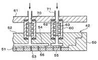
下部電極であるサセプタ13の上方には、上部電極42がサセプタ13に対向して平行に設けられている。上部電極42は、絶縁性の遮蔽部材50を介して処理容器11の上部に支持されている。この上部電極42は、ウェハチャック10に保持されたウェハWと対向面を形成する電極板51と、当該電極板51を上方から支持する電極支持体52とにより構成されている。電極板51には、処理容器11の内部に処理ガスを供給する複数のガス供給口53が当該電極板51を貫通して形成されている。電極板51には、例えばジュール熱の少ない低抵抗の導電体または半導体により構成され、本実施の形態においては例えばシリコンが用いられる。また、電極支持板52は導電体により構成され、本実施の形態においては例えばアルミニウムが用いられる。 Above the
また、上部電極42には、第1の高周波電源30及び第2の高周波電源40からの高周波をトラップするローパスフィルタ80を介して、直流電源81が電気的に接続されている。この直流電源81は、上部電極42側が負極、接地部材61側が正極となるように接続されている。これにより、上部電極42に負の直流電圧を印加することができる。本実施の形態においては、負の直流電圧の電圧は1200Vである。 A
第1の高周波電源30、第1の整合器31、第2の高周波電源40、第2の整合器41、直流電源81は、後述する制御部100に接続されており、これらの動作は制御部100により制御される。 The first high-
電極支持体52内部の中央部には、略円盤状に形成されたガス拡散室54が設けられている。ガス拡散室54の外方には、円環状に形成されたガス拡散室55がさらに設けられている。また、電極支持体52の下部には、ガス拡散室54、55から下方に伸びるガス孔56が複数形成され、ガス供給口53は当該ガス孔56を介してガス拡散室54、55に接続されている。なお、ガス拡散室54とガス拡散室55を別個に設けるのは、ガス拡散室54とガス拡散室55の内部の圧力をそれぞれ調整し、電極支持体52中央付近のガス孔56と外周部近傍のガス孔56から流れる処理ガスの流量を独立して調整するためであり、ガス拡散室54、55の配置や形状は本実施の形態に限定されるものではない。 A
電極支持体52の上方には、略円筒形状の絶縁部材60を介して、略円盤状の接地部材61が電極支持体52に対向して平行に設けられている。接地部材61は導電体により構成され、本実施の形態においては例えばアルミニウムが用いられる。 Above the
絶縁部材60の内部には、図2に示すように、ガス拡散室54、55に連通するガス流通路62が形成されている。このガス流通路62には、平面視において例えば接地部材61側の端部からガス流通路62を介して電極支持板52側の端部が視認できないように、当該ガス流通路62内を流れるガスを少なくとも水平成分を有する方向に流す屈曲部63が設けられている。本実施の形態における屈曲部63は、例えば図2に示すように、接地部材61側の端部から電極支持体52側の端部に向かって螺旋状にガスが流れるように形成されている。なお、水平成分を有する方向とは、水平方向のほかに、例えば斜め上方や斜め下方といった、鉛直方向以外の全ての方向を含んでいることを意味している。 As shown in FIG. 2, a
ガス流通路62に屈曲部63を設けることにより、図9に示される従来の絶縁部材203のように直線状にガス流通路212を設ける場合よりも、ガス流通路62の距離を長くすることができる。本実施の形態における屈曲部63は、ガス流通路62の距離が従来の絶縁部材203のガス流通路212の約3倍となるように構成されている。この屈曲部63により、放電電圧の決定因子である電極間の距離と電極間のガス圧力のうち、電極間の距離、即ち接地部材61と上部電極42と間のガス流通路62を長くすることができるので、直流電圧の印加に起因する放電の発生を抑制するように作用する。なお、ガス流通路62の長さをどの程度にするかは、ガス拡散室54、55内の圧力と印加する直流電圧との関係に基づき、放電が生じない範囲で任意に設定するものであり、本実施の形態に限定されるものではない。 By providing the
また、屈曲部63を設けることで、平面視においてガス流通路62の一の端部から他の端部が視認できないようになるので、当該屈曲部63が、上部電極42と接地部材61との間に直線的に放電が発生することを防止する障害物として機能する。したがって、直流電圧の印加に起因する放電の発生抑制を更に確実に行うことができる。 Further, by providing the
接地部材61には、ガス流通路62に対応する位置に、当該接地部材61を貫通してガス導入口70が形成されている。ガス導入口70には、ガス供給管71が接続されている。ガス供給管71には、図1に示すように処理ガス供給源72が接続されており、処理ガス供給源72から供給された処理ガスは、ガス供給管71及びガス流通路62を介してガス拡散室54、55に供給される。そして、ガス拡散室54、55に供給された処理ガスは、ガス孔56とガス供給口53を通じて処理容器11内に導入される。すなわち、上部電極42は、処理容器11内に処理ガスを供給するシャワーヘッドとして機能する。なお、処理ガスとしては、従来のプラズマエッチングに用いられている種々のものを採用することができ、例えばC4F8のようなフロロカーボンガスを用いてもよく、さらに、ArやO2といった他のガスが含まれていてもよい。In the grounding
ガス供給管71には、流量調整機構73が設けられており、処理ガス供給源72からガス拡散室54、55に供給するガスの量を制御することができる。流量調整機構73は、例えばマスフローコントローラとバルブにより構成されている。 The
処理容器11の底面には排気口90が設けられている。排気口90には排気管91を介して排気装置92が接続されており、当該排気装置92を駆動することにより処理容器11内の雰囲気を所定の真空度まで減圧することができる。また、処理容器11の内壁は、表面に耐プラズマ性の材料からなる溶射皮膜が形成されたライナ93により覆われている。 An
以上のプラズマ処理装置1には、既述のように制御部100が設けられている。制御部100は、例えばコンピュータであり、プログラム格納部(図示せず)を有している。プログラム格納部には、各電源30、40、81や各整合器31、41、及び流量調整機構73などを制御して、プラズマ処理装置1を動作させるためのプログラムも格納されている。 The
このプログラムは、例えば第1の高周波電源30のオン、オフ及び出力の制御が可能となっている。したがって、例えば第1の高周波電源30を連続的にオンにしてプラズマを連続的に生成したり、交互にオン、オフして高周波電力をパルス状に印加してプラズマが存在している状態とプラズマが消滅した状態を交互に形成したりすることができる。また、バイアス用の第2の高周波電源40についても第1の高周波電源30と同様にオン、オフ及び出力の制御が可能であり、プラズマ処理中に連続的にバイアスを印加したり、第1の高周波電源30のオン、オフに同期してパルス状にバイアスを印加したりすることが可能である。さらに、直流電源81のオン、オフ及び電圧と電流の制御を行うこともできる。 For example, this program can control the on / off and output of the first high-
なお、本実施の形態においては、例えば図3に示すように、第1の高周波電源30を交互にオン、オフさせ、それに同期して第2の高周波電源40を交互にオン、オフさせることで、プラズマが生成した状態とプラズマが消失した状態を交互に繰り返す。それと共に、第1の高周波電源30のオン、オフに同期して、直流電源81から上部電極42に、負の直流電圧を印加する。この際、印加される負の直流電圧の絶対値が、プラズマが生成している期間よりも、プラズマが消失している期間のほうが大きくなるように直流電源81が制御される。 In the present embodiment, for example, as shown in FIG. 3, the first high
このように各電源30、40、81を制御することで、電源30、40オンの期間においては第1の高周波電源30により生成されるプラズマのプラズマシースと、第2の高周波電源40により生成されるプラズマシースが重畳し、厚いプラズマシースが形成される。その結果、電源30、40オンの期間は電子がプラズマシースで反射されるが、電源30、40オフの期間はプラズマシースが消滅し、2次電子は容易にウェハWに到達する。 By controlling the
そしてこの間に、直流電源81により印加する負の直流電圧の絶対値が、プラズマが生成している期間よりも、プラズマが消失している期間のほうが大きくなるように印加することで、電源30、40オフの期間に多量の電子をウェハWの表面に供給することができる。そのため、正の電荷に帯電していたコンタクトホール内の電荷を中和することができるので、高周波電源をオンしてプラズマを生成した際に、正イオンがエッチングホール内で曲がることがなくなり、良好なエッチングを行えるようになる。 During this time, the absolute value of the negative DC voltage applied by the
なお、上記のプログラムは、例えばコンピュータ読み取り可能なハードディスク(HD)、フレキシブルディスク(FD)、コンパクトディスク(CD)、マグネットオプティカルデスク(MO)、メモリーカードなどのコンピュータに読み取り可能な記憶媒体Hに記録されていたものであって、その記憶媒体Hから制御部100にインストールされたものであってもよい。 The above program is recorded on a computer-readable storage medium H such as a computer-readable hard disk (HD), a flexible disk (FD), a compact disk (CD), a magnetic optical desk (MO), or a memory card. May have been installed in the
本実施の形態にかかるプラズマ処理装置1は以上のように構成されており、次に、本実施の形態にかかるプラズマ処理装置1におけるプラズマエッチング処理について説明する。 The
プラズマエッチング処理にあたっては、先ず、処理容器11内にウェハWが搬入され、ウェハチャック10上に載置されて保持される。次いで、排気装置92により処理容器11内を排気し、それと共に処理ガス供給源72から処理ガスを所定の流量で処理容器11内に供給する。この際、処理ガスの流量は、処理容器11内の圧力が、例えば10〜150Paの範囲内となるように流量調整機構73により調整される。 In the plasma etching process, first, the wafer W is loaded into the
その後、第1の高周波電源30と第2の高周波電源40により、下部電極であるサセプタ13に高周波電力を連続的に印加し、それと共に、直流電源81により上部電極42に直流電圧を連続的に印加する。これにより、処理容器11内に供給された処理ガスは、上部電極42とサセプタ13との間でプラズマ化される。 Thereafter, high frequency power is continuously applied to the
その後、各電源30、40、81を図3に示すパターンで制御し、処理容器11内のプラズマにより生成されるイオンやラジカルにより、ウェハWのエッチング処理が行われる。 Thereafter, the power supplies 30, 40, and 81 are controlled by the pattern shown in FIG. 3, and the wafer W is etched by ions and radicals generated by the plasma in the
この際、ガス流通路62には屈曲部63が設けられているので、接地部材61と上部電極42との間に、直流電圧の印加に起因する放電が生じることがなく、放電により生成した反応生成物のウェハ上への落下による半導体デバイス製品の歩留りの低下が回避できる。これにより高い負の直流電圧の印加が可能となるために従来に比べて高アスペクト比のエッチングホールを形成することができる。 At this time, since the
以上の実施の形態によれば、上部電極42と接地部材61との間に介在する絶縁部材60の内部に形成されたガス流通路62に、当該ガス流通路62を流れるガスが少なくとも水平成分を有する方向に流す屈曲部63が設けられ、これにより平面視において当該ガス流通路62の端部から他の端部が視認できないように構成されているので、従来のように、上部電極と接地部材との間にガス流通路を直線状に形成する場合よりも当該ガス流通路の距離を長くすることができる。これにより、放電電圧の決定因子である電極間の距離と電極間のガス圧力のうち、電極間の距離、即ち上部電極42と接地部材61との間の電気的な距離を、当該上部電極42と接地部材61との物理的な移動を伴うことなく、実質的に長くすることができる。したがって、直流電源81により従来よりも高い電圧で直流電圧を印加した場合であっても、当該直流電圧の印加に起因する放電の発生を抑制することができる。 According to the above embodiment, the gas flowing through the
また、ガス流通路62の距離が長くなることで、結果として当該ガス流通路62における処理ガスの圧力損失も大きくなる。したがって、ガス流通路62の両端部における圧力差が大きくなる、換言すれば、処理ガス供給源72から処理ガスが供給される際に、接地部材61側での処理ガスの圧力が上昇する。したがって、これによっても直流電圧の印加に起因する放電の発生を抑制することができる。 Further, as the distance of the
さらには、屈曲部63は、平面視においてガス流通路62の端部から他の端部が視認できないように形成されていることにより、当該屈曲部63が、上部電極42と接地部材61との間に直線的に放電が発生することを防止する障害物として機能する。したがって、以上の実施の形態によれば、直流電圧の印加に起因する放電の発生抑制を更に確実に行うことができる。 Furthermore, the
以上の実施の形態においては、ガス流通路62の屈曲部63は螺旋状に形成されていたが、ガス流通路62の形状は本実施の形態に限定されるものではなく、屈曲部63により、平面視においてガス流通路62の一の端部から他の端部が視認できなくなるように形成されていれば、様々な形状とすることができる。具体的には、例えば図4に示すように、屈曲部63の縦断面形状を略U字状にしたり、図5に示すように略V字状にしたりしてもよい。 In the above embodiment, the
また、図6に示すように、例えば接地部材61側の端部からガス流通路62を介して電極支持板52側の端部が視認できなくなるように、換言すれば、処理ガスがガス流通路62内を直進するのを妨げるように、当該ガス流通路62内部に整流部材110を設けると共に、整流部材110の外形形状に対応してこの屈曲部63を形成してもよい。さらには、整流部材110を例えば図示しない駆動機構に接続して移動自在とし、ガス流通路62の内部における整流部材110の上下方向の位置や左右方向の位置を変化させることで、ガス流通路62の圧力損失を状況に応じて調整するようにしてもよい。かかる場合、整流部材110を、例えばニードル弁の弁体といった、圧力調整により好ましい形状に形成してもよい。いずれの場合においても、当業者であれば、特許請求の範囲に記載された技術的思想の範疇内において、各種の変更例または修正例に想到しうることは明らかであり、それらについても当然に本発明の技術的範囲に属するものと了解される。 Further, as shown in FIG. 6, for example, the processing gas is introduced into the gas flow passage so that the end on the
なお、以上の実施の形態においては、ガス流通路62に屈曲部63を設けることで上部電極42と接地部材61との間の電気的な距離を長くするようにし、その結果、放電電圧の他方の決定因子である電極間のガス圧力も大きくなったが、電極間のガス圧力を積極的に大きくするために、例えばガス拡散室54、55側に処理ガスの圧力損失を増加させる抵抗部120を設けてもよい。 In the above embodiment, the
具体的には、例えば図7に示すように、電極支持板52のガス孔56の一部をオリフィス形状にする、即ち当該ガス孔56の中心部に向かって突出する円環状の突出部を設けることで抵抗部120を形成してもよい。また、例えば図8に示すように、電極板51のガス供給口53の一部をオリフィス形状にして、抵抗部120を形成してもよい。また、ガス孔56とガス供給口53の両方に抵抗部120を設けてもよく、ガス拡散室54、55とガス供給口53との間の管路抵抗を増加させることができれば、抵抗部120の形状や配置は任意に設定できる。したがって、例えばガス孔56の一部に突出部を設けるのではなく、ガス孔56全体にわたって当該ガス孔56の直径そのものを小さくした場合も、抵抗部120を形成しているといえる。いずれの場合においても、抵抗部120の前後での差圧が上昇し、それにより処理容器11内の圧力に対するガス拡散室54、55の圧力が高くなる。その結果として、ガス拡散室54、55の上流側であるガス流通路62における処理ガスの圧力も高くなり、これにより、直流電圧の印加に起因する放電の発生を抑制することができる。 Specifically, for example, as shown in FIG. 7, a part of the
特に、電極板51のガス供給口53は、処理容器11内のプラズマに曝されて浸食されることにより徐々にその直径が広がるため、経時的にガス供給口53そのものの管路抵抗が低下してしまう。その場合、ガス拡散室54、55内の処理ガスの圧力が低下し、その結果、ガス流通路62における圧力も低下して放電が起こり易くなる。そのため、従来は、定期的に電極板51を交換する必要があったが、本実施の形態のように抵抗部120を設けて圧力損失を確保して、ガス拡散室54、55の圧力を維持することで、経時的なガス圧力の低下を抑制できる。これにより、電極板51の交換頻度も低く抑えることができる。なお、上述のように、電極板51のガス供給口53は、処理容器11内のプラズマに曝されて浸食されるため、抵抗部120は、電極板51の下端面から所定の距離以上離れた位置に設けることが好ましい。 In particular, since the diameter of the
以上、本発明の好適な実施形態について説明したが、本発明はかかる例に限定されない。当業者であれば、特許請求の範囲に記載された技術的思想の範疇内において、各種の変更例または修正例に想到しうることは明らかであり、それらについても当然に本発明の技術的範囲に属するものと了解される。 As mentioned above, although preferred embodiment of this invention was described, this invention is not limited to this example. It is obvious for those skilled in the art that various changes or modifications can be conceived within the scope of the technical idea described in the claims. It is understood that it belongs to.
1 プラズマ処理装置
2 マイクロ波供給部
10 ウェハチャック
11 処理容器
12 接地線
13 サセプタ
14 絶縁板
15 支持台
20 補正リング
21 円筒部材
22 伝熱ガス管
30 第1の高周波電源
31 第1の整合器
40 第2の高周波電源
41 第2の整合器
42 上部電極
50 遮蔽部材
51 電極板
52 電極支持板
53 ガス供給口
54、55 ガス拡散室
56 ガス孔
60 絶縁部材
61 接地部材
62 ガス流通路
70 ガス導入口
71 ガス供給管
72 処理ガス供給源
73 流量調整機構
80 ローパスフィルタ
81 直流電源
90 排気口
91 排気管
92 排気装置
93 ライナ
100 制御部
110 整流部材
120 抵抗部
W ウェハ
DESCRIPTION OF
Claims (4)
Translated fromJapanese絶縁部材を介して前記上部電極の上方に設けられた接地部材と、
前記上部電極に負の直流電圧を印加する直流電源と、を有し、
前記上部電極の内部には、上部電極の下面に設けられたガス供給口に連通するガス拡散室が設けられ、
前記絶縁部材の内部には、前記ガス拡散室に連通するガス流通路が形成され、
前記ガス流通路には、平面視において当該ガス流通路の一の端部から他の端部が視認できないように、当該ガス流通路内を流れる処理ガスを少なくとも水平成分を有する方向に流す屈曲部が設けられ、
前記ガス流通路の屈曲部は、処理ガスが前記ガス流通路内を直進するのを妨げる整流部材を、当該ガス流通路の内部に設けることにより形成されており、
前記ガス流通路の内部において前記整流部材を移動させる駆動機構をさらに有していることを特徴とする、プラズマ処理装置。A plasma processing apparatus for applying a high frequency power between an upper electrode and a lower electrode provided in a processing container to convert a processing gas into plasma, and subjecting the target object to plasma processing with the plasma,
A grounding member provided above the upper electrode via an insulating member;
A DC power supply for applying a negative DC voltage to the upper electrode,
Inside the upper electrode, a gas diffusion chamber communicating with a gas supply port provided on the lower surface of the upper electrode is provided,
A gas flow path communicating with the gas diffusion chamber is formed inside the insulating member,
The gas flow passage has a bent portion for flowing aprocessing gas flowing in the gas flow passage in a direction having at least a horizontal component so that the other end portion cannot be visually recognized from one end portion of the gas flow passage in a plan view. Is provided,
The bent portion of the gas flow path is formed by providing a rectifying member that prevents the processing gas from going straight in the gas flow path inside the gas flow path,
The plasma processing apparatusfurther comprising a drive mechanism for moving the rectifying member inside the gas flow passage .
The upper electrode includes an electrode plate facing the object to be processed and an electrode support plate provided on the upper surface of the electrode plate, and the resistance portion is provided on the electrode plate side. The plasma processing apparatus according to claim2 .
Priority Applications (7)
| Application Number | Priority Date | Filing Date | Title |
|---|---|---|---|
| JP2012010445AJP5848140B2 (en) | 2012-01-20 | 2012-01-20 | Plasma processing equipment |
| TW102101532ATWI576911B (en) | 2012-01-20 | 2013-01-15 | Plasma processing device |
| CN201711079374.7ACN107833819B (en) | 2012-01-20 | 2013-01-16 | Plasma processing apparatus |
| CN201310015601.5ACN103219216B (en) | 2012-01-20 | 2013-01-16 | Plasma processing apparatus |
| US13/743,586US9055661B2 (en) | 2012-01-20 | 2013-01-17 | Plasma processing apparatus |
| KR1020130005717AKR101997823B1 (en) | 2012-01-20 | 2013-01-18 | Plasma processing apparatus |
| KR1020190079482AKR102098698B1 (en) | 2012-01-20 | 2019-07-02 | Plasma processing apparatus |
Applications Claiming Priority (1)
| Application Number | Priority Date | Filing Date | Title |
|---|---|---|---|
| JP2012010445AJP5848140B2 (en) | 2012-01-20 | 2012-01-20 | Plasma processing equipment |
Related Child Applications (1)
| Application Number | Title | Priority Date | Filing Date |
|---|---|---|---|
| JP2015230378ADivisionJP2016096342A (en) | 2015-11-26 | 2015-11-26 | Plasma processing device |
Publications (2)
| Publication Number | Publication Date |
|---|---|
| JP2013149865A JP2013149865A (en) | 2013-08-01 |
| JP5848140B2true JP5848140B2 (en) | 2016-01-27 |
Family
ID=48816903
Family Applications (1)
| Application Number | Title | Priority Date | Filing Date |
|---|---|---|---|
| JP2012010445AActiveJP5848140B2 (en) | 2012-01-20 | 2012-01-20 | Plasma processing equipment |
Country Status (5)
| Country | Link |
|---|---|
| US (1) | US9055661B2 (en) |
| JP (1) | JP5848140B2 (en) |
| KR (2) | KR101997823B1 (en) |
| CN (2) | CN107833819B (en) |
| TW (1) | TWI576911B (en) |
Families Citing this family (29)
| Publication number | Priority date | Publication date | Assignee | Title |
|---|---|---|---|---|
| US9574268B1 (en) | 2011-10-28 | 2017-02-21 | Asm America, Inc. | Pulsed valve manifold for atomic layer deposition |
| US9685297B2 (en) | 2012-08-28 | 2017-06-20 | Advanced Energy Industries, Inc. | Systems and methods for monitoring faults, anomalies, and other characteristics of a switched mode ion energy distribution system |
| JP6034655B2 (en)* | 2012-10-25 | 2016-11-30 | 東京エレクトロン株式会社 | Plasma processing equipment |
| US9275869B2 (en)* | 2013-08-02 | 2016-03-01 | Lam Research Corporation | Fast-gas switching for etching |
| KR101560623B1 (en)* | 2014-01-03 | 2015-10-15 | 주식회사 유진테크 | Substrate processing apparatus and substrate processing method |
| KR20160022458A (en) | 2014-08-19 | 2016-03-02 | 삼성전자주식회사 | Plasma apparatus and methdo of operating the same |
| JP6584786B2 (en)* | 2015-02-13 | 2019-10-02 | 株式会社日立ハイテクノロジーズ | Plasma ion source and charged particle beam device |
| JP6573252B2 (en)* | 2015-05-26 | 2019-09-11 | サムコ株式会社 | Substrate temperature adjustment mechanism for plasma processing equipment |
| US10233543B2 (en) | 2015-10-09 | 2019-03-19 | Applied Materials, Inc. | Showerhead assembly with multiple fluid delivery zones |
| US20190055648A1 (en)* | 2016-01-06 | 2019-02-21 | Toshiba Mitsubishi-Electric Insustrial Systems Cor | Gas supply apparatus |
| US11227748B2 (en)* | 2016-03-03 | 2022-01-18 | Core Technology, Inc. | Plasma treatment device and structure of reaction vessel for plasma treatment |
| CN107305830B (en)* | 2016-04-20 | 2020-02-11 | 中微半导体设备(上海)股份有限公司 | Capacitively coupled plasma processing apparatus and plasma processing method |
| US10662527B2 (en) | 2016-06-01 | 2020-05-26 | Asm Ip Holding B.V. | Manifolds for uniform vapor deposition |
| CN108573891B (en)* | 2017-03-07 | 2022-01-11 | 北京北方华创微电子装备有限公司 | Plasma processing apparatus |
| KR102096700B1 (en)* | 2017-03-29 | 2020-04-02 | 도쿄엘렉트론가부시키가이샤 | Substrate processing apparatus and substrate procesing method |
| JP7002268B2 (en)* | 2017-09-28 | 2022-01-20 | 東京エレクトロン株式会社 | Plasma processing equipment |
| US20240079213A9 (en)* | 2017-11-17 | 2024-03-07 | Advanced Energy Industries, Inc. | Synchronization of plasma processing components |
| KR102515110B1 (en)* | 2018-01-29 | 2023-03-28 | 주성엔지니어링(주) | Apparatus for Processing Substrate |
| CN108807127B (en)* | 2018-06-01 | 2020-03-31 | 北京北方华创微电子装备有限公司 | Upper electrode assembly, reaction chamber and atomic layer deposition equipment |
| JP6833784B2 (en)* | 2018-09-28 | 2021-02-24 | 芝浦メカトロニクス株式会社 | Plasma processing equipment |
| CN111383892B (en)* | 2018-12-29 | 2023-03-07 | 中微半导体设备(上海)股份有限公司 | Grounding connection structure of gas spray header in plasma processing device |
| US11492701B2 (en) | 2019-03-19 | 2022-11-08 | Asm Ip Holding B.V. | Reactor manifolds |
| US11881384B2 (en) | 2019-09-27 | 2024-01-23 | Applied Materials, Inc. | Monolithic modular microwave source with integrated process gas distribution |
| KR20210048408A (en) | 2019-10-22 | 2021-05-03 | 에이에스엠 아이피 홀딩 비.브이. | Semiconductor deposition reactor manifolds |
| CN113179676B (en)* | 2019-11-27 | 2024-04-09 | 东芝三菱电机产业系统株式会社 | Active gas generating device |
| CN111321463B (en)* | 2020-03-06 | 2021-10-15 | 北京北方华创微电子装备有限公司 | Reaction chamber |
| CN114914142B (en)* | 2021-02-08 | 2025-02-14 | 中微半导体设备(上海)股份有限公司 | Lower electrode assembly and plasma processing device |
| JP7575177B2 (en) | 2021-02-25 | 2024-10-29 | 東京エレクトロン株式会社 | Plasma processing apparatus and substrate support |
| JP7717015B2 (en)* | 2022-03-18 | 2025-08-01 | 東京エレクトロン株式会社 | Upper electrode and plasma processing apparatus |
Family Cites Families (20)
| Publication number | Priority date | Publication date | Assignee | Title |
|---|---|---|---|---|
| US6108189A (en)* | 1996-04-26 | 2000-08-22 | Applied Materials, Inc. | Electrostatic chuck having improved gas conduits |
| US6048435A (en)* | 1996-07-03 | 2000-04-11 | Tegal Corporation | Plasma etch reactor and method for emerging films |
| EP1008674B1 (en)* | 1997-04-11 | 2013-05-29 | Tokyo Electron Limited | Elecrode unit and processor |
| EP1523755B1 (en)* | 2002-07-23 | 2006-06-14 | Iplas Gmbh | Plasma reactor for carrying out gas reactions and method for the plasma-supported reaction of gases |
| JP4493932B2 (en)* | 2003-05-13 | 2010-06-30 | 東京エレクトロン株式会社 | Upper electrode and plasma processing apparatus |
| TWI574318B (en)* | 2004-06-21 | 2017-03-11 | Tokyo Electron Ltd | A plasma processing apparatus, a plasma processing method, and a computer-readable recording medium |
| US7988816B2 (en)* | 2004-06-21 | 2011-08-02 | Tokyo Electron Limited | Plasma processing apparatus and method |
| JP4572100B2 (en)* | 2004-09-28 | 2010-10-27 | 日本エー・エス・エム株式会社 | Plasma processing equipment |
| KR100954128B1 (en)* | 2006-01-20 | 2010-04-20 | 도쿄엘렉트론가부시키가이샤 | The top plate used for a plasma processing apparatus, a plasma processing apparatus, and the manufacturing method of a top plate |
| WO2007105411A1 (en)* | 2006-03-07 | 2007-09-20 | University Of The Ryukyus | Plasma generator and method of generating plasma using the same |
| US20070281106A1 (en)* | 2006-05-30 | 2007-12-06 | Applied Materials, Inc. | Process chamber for dielectric gapfill |
| JP4826483B2 (en)* | 2007-01-19 | 2011-11-30 | 東京エレクトロン株式会社 | Plasma processing equipment |
| US8069817B2 (en)* | 2007-03-30 | 2011-12-06 | Lam Research Corporation | Showerhead electrodes and showerhead electrode assemblies having low-particle performance for semiconductor material processing apparatuses |
| JP5008478B2 (en)* | 2007-06-27 | 2012-08-22 | 東京エレクトロン株式会社 | Substrate processing apparatus and shower head |
| EP2215282B1 (en)* | 2007-10-11 | 2016-11-30 | Valence Process Equipment, Inc. | Chemical vapor deposition reactor |
| WO2009133189A1 (en)* | 2008-05-02 | 2009-11-05 | Oerlikon Trading Ag, Truebbach | Plasma processing apparatus and method for the plasma processing of substrates |
| US8383001B2 (en)* | 2009-02-20 | 2013-02-26 | Tokyo Electron Limited | Plasma etching method, plasma etching apparatus and storage medium |
| JP5466480B2 (en) | 2009-02-20 | 2014-04-09 | 東京エレクトロン株式会社 | Plasma etching method, plasma etching apparatus and storage medium |
| KR101612741B1 (en)* | 2010-03-08 | 2016-04-18 | 주성엔지니어링(주) | Gas distributing plate and Apparatus for treating substrate including the same |
| US9082593B2 (en)* | 2011-03-31 | 2015-07-14 | Tokyo Electron Limited | Electrode having gas discharge function and plasma processing apparatus |
- 2012
- 2012-01-20JPJP2012010445Apatent/JP5848140B2/enactiveActive
- 2013
- 2013-01-15TWTW102101532Apatent/TWI576911B/enactive
- 2013-01-16CNCN201711079374.7Apatent/CN107833819B/enactiveActive
- 2013-01-16CNCN201310015601.5Apatent/CN103219216B/enactiveActive
- 2013-01-17USUS13/743,586patent/US9055661B2/enactiveActive
- 2013-01-18KRKR1020130005717Apatent/KR101997823B1/enactiveActive
- 2019
- 2019-07-02KRKR1020190079482Apatent/KR102098698B1/enactiveActive
Also Published As
| Publication number | Publication date |
|---|---|
| CN103219216A (en) | 2013-07-24 |
| TWI576911B (en) | 2017-04-01 |
| JP2013149865A (en) | 2013-08-01 |
| CN103219216B (en) | 2017-11-28 |
| KR20130085984A (en) | 2013-07-30 |
| KR101997823B1 (en) | 2019-07-08 |
| US9055661B2 (en) | 2015-06-09 |
| CN107833819B (en) | 2020-05-08 |
| US20130206338A1 (en) | 2013-08-15 |
| CN107833819A (en) | 2018-03-23 |
| TW201349337A (en) | 2013-12-01 |
| KR102098698B1 (en) | 2020-04-08 |
| KR20190082721A (en) | 2019-07-10 |
Similar Documents
| Publication | Publication Date | Title |
|---|---|---|
| JP5848140B2 (en) | Plasma processing equipment | |
| JP6671446B2 (en) | Pulse plasma chamber with dual chamber configuration | |
| TWI861122B (en) | Stage and plasma processing apparatus | |
| JP5221403B2 (en) | Plasma etching method, plasma etching apparatus and storage medium | |
| JP6539113B2 (en) | Plasma processing apparatus and plasma processing method | |
| JP4753276B2 (en) | Plasma processing method and plasma processing apparatus | |
| US9508530B2 (en) | Plasma processing chamber with flexible symmetric RF return strap | |
| JP4482308B2 (en) | Plasma processing apparatus and plasma processing method | |
| KR100886982B1 (en) | Plasma processing apparatus and plasma processing method | |
| TWI428061B (en) | Field enhanced inductively coupled plasma (fe-icp) reactor | |
| JP5231038B2 (en) | Plasma processing apparatus, plasma processing method, and storage medium | |
| US9502219B2 (en) | Plasma processing method | |
| JP7140610B2 (en) | Plasma processing equipment | |
| CN106356274A (en) | Extreme edge sheath and wafer profile tuning through edge-localized ion trajectory control and plasma operation | |
| JPWO2013125523A1 (en) | Power supply system, plasma etching apparatus and plasma etching method | |
| JP5951324B2 (en) | Plasma processing equipment | |
| JP7576484B2 (en) | Etching method and plasma processing apparatus | |
| JP2021141188A (en) | Plasma processing equipment, semiconductor members, and edge rings | |
| CN111952140B (en) | Substrate mounting table and plasma processing apparatus | |
| JP2016096342A (en) | Plasma processing device | |
| US12002659B2 (en) | Apparatus for generating etchants for remote plasma processes | |
| JP2017224697A (en) | Gas transport tube and plasma processing apparatus |
Legal Events
| Date | Code | Title | Description |
|---|---|---|---|
| A621 | Written request for application examination | Free format text:JAPANESE INTERMEDIATE CODE: A621 Effective date:20141010 | |
| A977 | Report on retrieval | Free format text:JAPANESE INTERMEDIATE CODE: A971007 Effective date:20150615 | |
| A131 | Notification of reasons for refusal | Free format text:JAPANESE INTERMEDIATE CODE: A131 Effective date:20150623 | |
| A521 | Request for written amendment filed | Free format text:JAPANESE INTERMEDIATE CODE: A523 Effective date:20150821 | |
| TRDD | Decision of grant or rejection written | ||
| A01 | Written decision to grant a patent or to grant a registration (utility model) | Free format text:JAPANESE INTERMEDIATE CODE: A01 Effective date:20151027 | |
| A61 | First payment of annual fees (during grant procedure) | Free format text:JAPANESE INTERMEDIATE CODE: A61 Effective date:20151126 | |
| R150 | Certificate of patent or registration of utility model | Ref document number:5848140 Country of ref document:JP Free format text:JAPANESE INTERMEDIATE CODE: R150 | |
| R250 | Receipt of annual fees | Free format text:JAPANESE INTERMEDIATE CODE: R250 | |
| R250 | Receipt of annual fees | Free format text:JAPANESE INTERMEDIATE CODE: R250 | |
| R250 | Receipt of annual fees | Free format text:JAPANESE INTERMEDIATE CODE: R250 | |
| R250 | Receipt of annual fees | Free format text:JAPANESE INTERMEDIATE CODE: R250 | |
| R250 | Receipt of annual fees | Free format text:JAPANESE INTERMEDIATE CODE: R250 | |
| R250 | Receipt of annual fees | Free format text:JAPANESE INTERMEDIATE CODE: R250 | |
| R250 | Receipt of annual fees | Free format text:JAPANESE INTERMEDIATE CODE: R250 |