JP5845568B2 - Semiconductor device and manufacturing method thereof - Google Patents
Semiconductor device and manufacturing method thereofDownload PDFInfo
- Publication number
- JP5845568B2 JP5845568B2JP2010246743AJP2010246743AJP5845568B2JP 5845568 B2JP5845568 B2JP 5845568B2JP 2010246743 AJP2010246743 AJP 2010246743AJP 2010246743 AJP2010246743 AJP 2010246743AJP 5845568 B2JP5845568 B2JP 5845568B2
- Authority
- JP
- Japan
- Prior art keywords
- layer
- electrode
- signal line
- gate electrode
- nitride semiconductor
- Prior art date
- Legal status (The legal status is an assumption and is not a legal conclusion. Google has not performed a legal analysis and makes no representation as to the accuracy of the status listed.)
- Expired - Fee Related
Links
Images


Classifications
- H—ELECTRICITY
- H10—SEMICONDUCTOR DEVICES; ELECTRIC SOLID-STATE DEVICES NOT OTHERWISE PROVIDED FOR
- H10D—INORGANIC ELECTRIC SEMICONDUCTOR DEVICES
- H10D30/00—Field-effect transistors [FET]
- H10D30/40—FETs having zero-dimensional [0D], one-dimensional [1D] or two-dimensional [2D] charge carrier gas channels
- H10D30/47—FETs having zero-dimensional [0D], one-dimensional [1D] or two-dimensional [2D] charge carrier gas channels having 2D charge carrier gas channels, e.g. nanoribbon FETs or high electron mobility transistors [HEMT]
- H10D30/471—High electron mobility transistors [HEMT] or high hole mobility transistors [HHMT]
- H10D30/475—High electron mobility transistors [HEMT] or high hole mobility transistors [HHMT] having wider bandgap layer formed on top of lower bandgap active layer, e.g. undoped barrier HEMTs such as i-AlGaN/GaN HEMTs
- H10D30/4755—High electron mobility transistors [HEMT] or high hole mobility transistors [HHMT] having wider bandgap layer formed on top of lower bandgap active layer, e.g. undoped barrier HEMTs such as i-AlGaN/GaN HEMTs having wide bandgap charge-carrier supplying layers, e.g. modulation doped HEMTs such as n-AlGaAs/GaAs HEMTs
- H—ELECTRICITY
- H01—ELECTRIC ELEMENTS
- H01L—SEMICONDUCTOR DEVICES NOT COVERED BY CLASS H10
- H01L21/00—Processes or apparatus adapted for the manufacture or treatment of semiconductor or solid state devices or of parts thereof
- H01L21/02—Manufacture or treatment of semiconductor devices or of parts thereof
- H01L21/04—Manufacture or treatment of semiconductor devices or of parts thereof the devices having potential barriers, e.g. a PN junction, depletion layer or carrier concentration layer
- H01L21/18—Manufacture or treatment of semiconductor devices or of parts thereof the devices having potential barriers, e.g. a PN junction, depletion layer or carrier concentration layer the devices having semiconductor bodies comprising elements of Group IV of the Periodic Table or AIIIBV compounds with or without impurities, e.g. doping materials
- H—ELECTRICITY
- H10—SEMICONDUCTOR DEVICES; ELECTRIC SOLID-STATE DEVICES NOT OTHERWISE PROVIDED FOR
- H10D—INORGANIC ELECTRIC SEMICONDUCTOR DEVICES
- H10D30/00—Field-effect transistors [FET]
- H10D30/01—Manufacture or treatment
- H10D30/015—Manufacture or treatment of FETs having heterojunction interface channels or heterojunction gate electrodes, e.g. HEMT
- H—ELECTRICITY
- H10—SEMICONDUCTOR DEVICES; ELECTRIC SOLID-STATE DEVICES NOT OTHERWISE PROVIDED FOR
- H10D—INORGANIC ELECTRIC SEMICONDUCTOR DEVICES
- H10D62/00—Semiconductor bodies, or regions thereof, of devices having potential barriers
- H10D62/10—Shapes, relative sizes or dispositions of the regions of the semiconductor bodies; Shapes of the semiconductor bodies
- H10D62/17—Semiconductor regions connected to electrodes not carrying current to be rectified, amplified or switched, e.g. channel regions
- H10D62/213—Channel regions of field-effect devices
- H10D62/221—Channel regions of field-effect devices of FETs
- H—ELECTRICITY
- H10—SEMICONDUCTOR DEVICES; ELECTRIC SOLID-STATE DEVICES NOT OTHERWISE PROVIDED FOR
- H10D—INORGANIC ELECTRIC SEMICONDUCTOR DEVICES
- H10D84/00—Integrated devices formed in or on semiconductor substrates that comprise only semiconducting layers, e.g. on Si wafers or on GaAs-on-Si wafers
- H10D84/01—Manufacture or treatment
- H10D84/02—Manufacture or treatment characterised by using material-based technologies
- H10D84/05—Manufacture or treatment characterised by using material-based technologies using Group III-V technology
- H—ELECTRICITY
- H10—SEMICONDUCTOR DEVICES; ELECTRIC SOLID-STATE DEVICES NOT OTHERWISE PROVIDED FOR
- H10D—INORGANIC ELECTRIC SEMICONDUCTOR DEVICES
- H10D62/00—Semiconductor bodies, or regions thereof, of devices having potential barriers
- H10D62/80—Semiconductor bodies, or regions thereof, of devices having potential barriers characterised by the materials
- H10D62/85—Semiconductor bodies, or regions thereof, of devices having potential barriers characterised by the materials being Group III-V materials, e.g. GaAs
- H10D62/8503—Nitride Group III-V materials, e.g. AlN or GaN
Landscapes
- Engineering & Computer Science (AREA)
- Physics & Mathematics (AREA)
- Condensed Matter Physics & Semiconductors (AREA)
- General Physics & Mathematics (AREA)
- Manufacturing & Machinery (AREA)
- Computer Hardware Design (AREA)
- Microelectronics & Electronic Packaging (AREA)
- Power Engineering (AREA)
- Junction Field-Effect Transistors (AREA)
Description
Translated fromJapanese本発明は、半導体装置及びその製造方法に関する。 The present invention relates to a semiconductor device and a manufacturing method thereof.
従来、基板の上方に結晶成長によりAlGaN層及びGaN層が形成され、GaN層が電子走行層として機能する高電子移動度トランジスタ(HEMT:high electron mobility transistor)についての研究が行われている。GaNのバンドギャップは3.4eVであり、Siのバンドギャップ(1.1eV)及びGaAsのバンドギャップ(1.4eV)よりも大きい。このため、GaN系のHEMTの耐圧は高く、自動車用等の高耐圧電力デバイスとして有望である。 Conventionally, research has been conducted on a high electron mobility transistor (HEMT) in which an AlGaN layer and a GaN layer are formed by crystal growth above a substrate, and the GaN layer functions as an electron transit layer. The band gap of GaN is 3.4 eV, which is larger than the band gap of Si (1.1 eV) and the band gap of GaAs (1.4 eV). For this reason, the GaN-based HEMT has a high withstand voltage and is promising as a high withstand voltage power device for automobiles and the like.
このようなHEMTは、主としてゲートドライバが搭載された回路基板等に搭載され、当該ゲートドライバに接続されて用いられる。つまり、HEMTのゲートには、回路基板に形成された回路等を介して、ゲートドライバからオン/オフ制御の電圧が供給される。 Such a HEMT is mainly mounted on a circuit board or the like on which a gate driver is mounted, and is used by being connected to the gate driver. That is, an ON / OFF control voltage is supplied to the gate of the HEMT from the gate driver via a circuit or the like formed on the circuit board.
しかしながら、回路基板に形成された回路等を介した駆動では、ゲートドライバとHEMTとの間のインダクタンス成分が大きいため、HEMTを十分に高速動作させることが困難である。また、従来、ゲートドライバとHEMTとを一つのチップ内に収納することも困難である。 However, in driving through a circuit or the like formed on a circuit board, it is difficult to operate the HEMT sufficiently fast because the inductance component between the gate driver and the HEMT is large. Conventionally, it is also difficult to accommodate the gate driver and the HEMT in one chip.
本発明の目的は、トランジスタをより高速に動作させることができる半導体装置及びその製造方法を提供することにある。 An object of the present invention is to provide a semiconductor device capable of operating a transistor at higher speed and a manufacturing method thereof.
半導体装置の一態様には、基板と、前記基板の上方に形成された、ゲート電極、電子走行層及び電子供給層を備えたトランジスタと、前記電子供給層上方に形成された絶縁層と、前記絶縁層の上方に形成された窒化物半導体層と、前記窒化物半導体層上方に、平面視で前記ゲート電極を間に挟むようにして形成された第1の電極及び第2の電極と、前記窒化物半導体層上方で、かつ平面視で前記ゲート電極と前記第1の電極との間に形成された第1の信号ラインと、前記窒化物半導体層上方で、かつ平面視で前記ゲート電極と前記第2の電極との間に形成された第2の信号ラインと、が設けられている。前記ゲート電極は、前記絶縁層より上方に位置して前記窒化物半導体層と接する部分を有する。前記第1の信号ラインは、前記ゲート電極と前記第1の電極との間で前記窒化物半導体層を移動する電荷を制御し、前記第2の信号ラインは、前記ゲート電極と前記第2の電極との間で前記窒化物半導体層を移動する電荷を制御する。In one aspect of the semiconductor device, a substrate, a transistor including a gate electrode, an electron transit layer, and an electron supply layer formed over the substrate, an insulating layer formed over the electron supply layer, A nitride semiconductor layer formed above an insulating layer; a first electrode and a second electrode formed above the nitride semiconductor layer so as to sandwich the gate electrode therebetween in plan view; and the nitride A first signal line formed above the semiconductor layer and between the gate electrode and the first electrode in plan view; and the gate electrode and the first signal line above the nitride semiconductor layer and in plan view. And a second signal line formed between the two electrodes. The gate electrode has a portion located above the insulating layer and in contact with the nitride semiconductor layer.The first signal line controls a charge moving through the nitride semiconductor layer between the gate electrode and the first electrode, and the second signal line includes the gate electrode and the second electrode. The electric charge which moves the said nitride semiconductor layer between electrodes is controlled.
上記の半導体装置等によれば、トランジスタのゲートの駆動を高速で行うことができ、トランジスタをより高速に動作させることができる。 According to the above semiconductor device or the like, the gate of the transistor can be driven at high speed, and the transistor can be operated at higher speed.
以下、本発明の実施形態について、添付の図面を参照して具体的に説明する。 Hereinafter, embodiments of the present invention will be specifically described with reference to the accompanying drawings.
(第1の実施形態)
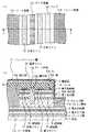
先ず、第1の実施形態に係る半導体装置について説明する。図1(a)は、第1の実施形態に係る半導体装置の電極等の位置関係を示す平面図であり、図1(b)は、第1の実施形態に係る半導体装置の構造を示す断面図である。図1(b)は、図1(a)中のI−I線に沿った断面を示している。(First embodiment)
First, the semiconductor device according to the first embodiment will be described. FIG. 1A is a plan view showing the positional relationship of electrodes and the like of the semiconductor device according to the first embodiment, and FIG. 1B is a cross-sectional view showing the structure of the semiconductor device according to the first embodiment. FIG. FIG.1 (b) has shown the cross section along the II line | wire in Fig.1 (a).
図1(a)及び(b)に示すように、第1の実施形態では、基板1上に、バッファ層2、電子走行層3、電子供給層4、キャップ層5、絶縁層6、電子走行層7、及び電子供給層8がこの順で形成されている。基板1としては、例えばn型のSi基板が用いられる。バッファ層2としては、例えばAlN層が形成されており、その厚さは、例えば1nm〜1000nmである。電子走行層3としては、例えば真性GaN層が形成されており、その厚さは、例えば10nm〜5000nmである。電子供給層4としては、例えばAl0.25Ga0.75N層が形成されており、その厚さは、例えば1nm〜100nmである。キャップ層5としては、例えばn型のGaN層が形成されており、その厚さは、例えば1nm〜100nmである。キャップ層5には、例えばSiがドーピングされている。絶縁層6としては、例えばAlN層が形成されており、その厚さは、例えば10nm〜5000nmである。絶縁層6として、AlGaN層、p型GaN層、FeドープGaN層、Si酸化物層、Al酸化物層、Si窒化物層、又はC層が形成されていてもよい。また、AlN層、AlGaN層、p型GaN層、FeドープGaN層、Si酸化物層、Al酸化物層、Si窒化物層、及びC層のうちの1種以上が絶縁層6に含まれていてもよい。電子走行層7としては、例えば真性GaN層が形成されており、その厚さは、例えば10nm〜5000nmである。電子供給層8としては、例えばAl0.25Ga0.75N層が形成されており、その厚さは、例えば1nm〜100nmである。As shown in FIGS. 1A and 1B, in the first embodiment, a
電子供給層8、電子走行層7、及び絶縁層6には、キャップ層5の厚さ方向の一部まで入り込むゲート電極用の開口部10gが形成されている。また、電子供給層8、電子走行層7、絶縁層6、及びキャップ層5には、平面視で開口部10gを間に挟むようにして、ソース電極用の開口部10s及びドレイン電極用の開口部10dが形成されている。そして、開口部10g内にゲート電極11gが形成され、開口部10s内にソース電極11sが形成され、開口部10d内にドレイン電極11dが形成されている。例えば、ゲート電極11g及びソース電極11sの上面は、電子供給層8の上面よりも高い位置にあり、ドレイン電極11dの上面は、絶縁層6の上面とキャップ層5の上面との間に位置する。 In the
電子供給層8上に、信号ライン12、信号ライン13、及びパッド14が形成されている。信号ライン12と電子供給層8との間には絶縁膜18が介在し、信号ライン13と電子供給層8との間には絶縁膜19が介在している。信号ライン12は、平面視で、ゲート電極11gとソース電極11sとの間に介在し、ゲート電極11g及びソース電極11s間の領域を二分する。信号ライン13は、平面視で、ゲート電極11gとドレイン電極11dとの間に介在し、ゲート電極11g及びドレイン電極11d間の領域を二分する。また、パッド14は、平面視で、信号ライン13とドレイン電極11dとの間に介在し、信号ライン13及びドレイン電極11d間の領域を二分する。つまり、信号ライン13は、平面視で、ゲート電極11gとパッド14との間に介在し、ゲート電極11g及びパッド14間の領域を二分している。 A
ゲート電極11g、ソース電極11s、信号ライン12、信号ライン13、及びパッド14を覆う絶縁層9が形成されている。絶縁層9としては、例えばシリコン窒化物層が形成されており、その厚さは、例えば0.1nm〜5000nmである。絶縁層9には、パッド14まで到達する孔15a及びこの孔15aに連通する溝15bが形成されており、孔15a内及び溝15b内に電源ライン16が埋め込まれている。 An insulating
絶縁層9、電源ライン16、及びドレイン電極11dを覆うパッシベーション膜17が形成されている。パッシベーション膜17に、電源ライン16の一部を露出する開口部、及びドレイン電極11dの一部を露出する開口部が形成されている。パッシベーション膜17及び絶縁層9に、ソース電極11sの一部を露出する開口部が形成されている。これらの開口部を介して、図2に示すように、電源ライン16が外部端子51に接続され、ソース電極11sが外部端子52に接続され、ドレイン電極11dが外部端子53に接続される。また、信号ライン12及び13は、基板1上に形成されたゲートドライバに接続される。例えば、このゲートドライバもパッシベーション膜17に覆われる。 A passivation film 17 is formed to cover the insulating
このように構成された半導体装置には、ゲート電極11g、ソース電極11s及びドレイン電極11dを備えたGaN系のHEMTが含まれる。そして、例えば、ソース電極11sは外部端子52を介して接地され、電源ライン16は外部端子51を介して12Vの電源に接続され、ドレイン電極11dには外部端子53を介してHEMTの用途に応じた所定の電圧が供給される。また、ゲートドライバから、信号ライン12に0V又は12Vの電圧が印加され、信号ライン13に24V又は0Vの電圧が印加される。従って、ゲート電極11gには、信号ライン12に印加される電圧及び信号ライン13に印加される電圧に応じた電圧が印加され、この電圧に応じてHEMTのオン/オフが切り替えられる。即ち、HEMTのオン/オフの切り替えは、下記表1に示す電圧制御により行われる。 The semiconductor device configured in this way includes a GaN-based HEMT including a

表1に示すように、信号ライン12にオン電圧が印加されるタイミングでは、信号ライン13にオフ電圧が印加され、信号ライン12にオフ電圧が印加されるタイミングでは、信号ライン13にオン電圧が印加される。そして、この電圧制御の際には、基板1上に形成されたゲートドライバから信号ライン12及び13に電圧が印加され、GaN系材料の電子走行層7を電子が高速で移動する。従って、Si系トランジスタを用いてHEMTのゲート電圧を印加する場合と比較して、HEMTをより高速に動作させることが可能である。 As shown in Table 1, when the on-voltage is applied to the
次に、第1の実施形態に係る半導体装置を製造する方法について説明する。図3A乃至図3Cは、第1の実施形態に係る半導体装置の製造方法を工程順に示す断面図である。 Next, a method for manufacturing the semiconductor device according to the first embodiment will be described. 3A to 3C are cross-sectional views illustrating the method of manufacturing the semiconductor device according to the first embodiment in the order of steps.
先ず、図3A(a)に示すように、基板1上に、例えば有機化学気相堆積(MOCVD:metal organic chemical vapor deposition)法により、バッファ層2、電子走行層3、電子供給層4、キャップ層5、絶縁層6、電子走行層7、及び電子供給層8を形成する。 First, as shown in FIG. 3A (a), a
ここで、MOCVD装置について説明する。図4は、MOCVD装置の構成を示す図である。石英製反応管140の周囲に高周波コイル141が配置され、反応管140の内側に基板120を載置するためのカーボンサセプタ142が配置されている。反応管140の上流端(図4中の左側の端部)に、2本のガス導入管144及び145が接続され、化合物のソースガスが供給される。例えば、ガス導入管144からNソースガスとしてNH3ガスが導入され、ガス導入管145からIII族元素のソースガスとしてトリメチルアルミニウム(TMA)、トリメチルガリウム(TMG)等の有機III族化合物原料が導入される。基板120上で結晶成長が行われ、余剰のガスはガス排出管146から除害塔へ排出される。なお、MOCVD法による結晶成長を減圧雰囲気で行う場合は、ガス排出管146は真空ポンプへ接続され、真空ポンプの排出口が除害塔に接続される。Here, the MOCVD apparatus will be described. FIG. 4 is a diagram showing the configuration of the MOCVD apparatus. A high frequency coil 141 is disposed around the quartz reaction tube 140, and a carbon susceptor 142 for placing the
バッファ層2としてAlN層を形成する場合の条件は、例えば、以下のように設定する。
トリメチルアルミニウム(TMA)の流量:1〜50sccm、
アンモニア(NH3)の流量:10〜5000sccm、
圧力:100Torr、
温度:1100℃。Conditions for forming an AlN layer as the
Trimethylaluminum (TMA) flow rate: 1-50 sccm,
Ammonia (NH3 ) flow rate: 10-5000 sccm,
Pressure: 100 Torr,
Temperature: 1100 ° C.
電子走行層3として真性GaN層を形成する場合の条件は、例えば、以下のように設定する。
トリメチルガリウム(TMG)の流量:1〜50sccm、
アンモニア(NH3)の流量:10〜10000sccm、
圧力:100Torr、
温度:1100℃。Conditions for forming an intrinsic GaN layer as the electron transit layer 3 are set as follows, for example.
Trimethylgallium (TMG) flow rate: 1-50 sccm,
Ammonia (NH3 ) flow rate: 10-10000 sccm,
Pressure: 100 Torr,
Temperature: 1100 ° C.
電子供給層4としてAl0.25Ga0.75N層を形成する場合の条件は、例えば、以下のように設定する。
トリメチルガリウム(TMG)の流量:0〜50sccm、
トリメチルアルミニウム(TMA)の流量:0〜50sccm、
アンモニア(NH3)の流量:20slm、
圧力:100Torr、
温度:1100℃。Conditions for forming an Al0.25 Ga0.75 N layer as the
Trimethylgallium (TMG) flow rate: 0-50 sccm,
Trimethylaluminum (TMA) flow rate: 0-50 sccm,
Ammonia (NH3 ) flow rate: 20 slm,
Pressure: 100 Torr,
Temperature: 1100 ° C.
キャップ層5としてn型のGaN層を形成する場合の条件は、例えば、以下のように設定する。
トリメチルガリウム(TMG)の流量:1〜50sccm、
アンモニア(NH3)の流量:10〜10000sccm、
n型不純物:シラン(SiH4)、
圧力:100Torr、
温度:1100℃。Conditions for forming an n-type GaN layer as the
Trimethylgallium (TMG) flow rate: 1-50 sccm,
Ammonia (NH3 ) flow rate: 10-10000 sccm,
n-type impurity: silane (SiH4 ),
Pressure: 100 Torr,
Temperature: 1100 ° C.
絶縁層6としてAlN層を形成する場合の条件は、例えば、以下のように設定する。
トリメチルアルミニウム(TMA)の流量:1〜50sccm、
アンモニア(NH3)の流量:10〜5000sccm、
圧力:100Torr、
温度:1100℃。Conditions for forming an AlN layer as the insulating
Trimethylaluminum (TMA) flow rate: 1-50 sccm,
Ammonia (NH3 ) flow rate: 10-5000 sccm,
Pressure: 100 Torr,
Temperature: 1100 ° C.
電子走行層7として真性GaN層を形成する場合の条件は、例えば、以下のように設定する。
トリメチルガリウム(TMG)の流量:1〜50sccm、
アンモニア(NH3)の流量:10〜10000sccm、
圧力:100Torr、
温度:1100℃。Conditions for forming an intrinsic GaN layer as the
Trimethylgallium (TMG) flow rate: 1-50 sccm,
Ammonia (NH3 ) flow rate: 10-10000 sccm,
Pressure: 100 Torr,
Temperature: 1100 ° C.
電子供給層8としてAl0.25Ga0.75N層を形成する場合の条件は、例えば、以下のように設定する。
トリメチルガリウム(TMG)の流量:0〜50sccm、
トリメチルアルミニウム(TMA)の流量:0〜50sccm、
アンモニア(NH3)の流量:20slm、
圧力:100Torr、
温度:1100℃。Conditions for forming an Al0.25 Ga0.75 N layer as the
Trimethylgallium (TMG) flow rate: 0-50 sccm,
Trimethylaluminum (TMA) flow rate: 0-50 sccm,
Ammonia (NH3 ) flow rate: 20 slm,
Pressure: 100 Torr,
Temperature: 1100 ° C.
次いで、図3A(b)に示すように、ゲート電極用の開口部10g、ソース電極用の開口部10s及びドレイン電極用の開口部10dを形成する。開口部10s及び10dは同時に形成することが好ましいが、開口部10gはこれらとは別に形成することが好ましい。深さが異なるからである。開口部10gの形成に際しては、例えば開口部10gを形成する予定の領域を露出するレジストパターンを形成し、このレジストパターンをマスクとして、電子供給層8、電子走行層7、絶縁層6、及びキャップ層5の一部をエッチングすればよい。その後、レジストパターンは除去する。開口部10s及び10dの形成に際しては、例えば開口部10s及び10dを形成する予定の領域を露出するレジストパターンを形成し、このレジストパターンをマスクとして、電子供給層8、電子走行層7、絶縁層6、及びキャップ層5をエッチングすればよい。その後、レジストパターンは除去する。 Next, as shown in FIG. 3A (b), an
その後、図3B(c)に示すように、ゲート電極11gを形成し、ソース電極11s及びドレイン電極11dを形成し、絶縁膜18、絶縁膜19、信号ライン12、及び信号ライン13を形成し、パッド14を形成する。これらの形成順序は特に限定されない。これらは、例えばリフトオフ法により形成することができる。 Thereafter, as shown in FIG. 3B (c), the
続いて、図3B(d)に示すように、全面に絶縁層9を形成し、この絶縁層9に、溝15b及び孔15aを形成する。また、ドレイン電極11dを露出させる。絶縁層9は、例えばプラズマCVD法により形成する。また、溝15b及び孔15aの形成並びにドレイン電極11dの露出の際には、例えば、レジストパターンをマスクとし、SF6ガスをエッチングガスとして用いる選択エッチングを行う。Subsequently, as shown in FIG. 3B (d), an insulating
次いで、図3C(e)に示すように、溝15b及び孔15a内に電源ライン16を形成する。電源ライン16は、例えばリフトオフ法により形成することができる。 Next, as shown in FIG. 3C (e), the
その後、図3C(f)に示すように、表面全体を覆うパッシベーション膜17を形成し、パッシベーション膜17に、電源ライン16の一部を露出する開口部、及びドレイン電極11dの一部を露出する開口部を形成する。また、パッシベーション膜17及び絶縁層9に、ソース電極11sの一部を露出する開口部を形成する。 Thereafter, as shown in FIG. 3C (f), a passivation film 17 covering the entire surface is formed, and an opening for exposing a part of the
このようにして半導体装置を完成させることができる。必要に応じて、基板1の裏面を研磨して半導体装置の厚さを調整してもよい。 In this way, the semiconductor device can be completed. If necessary, the thickness of the semiconductor device may be adjusted by polishing the back surface of the
なお、ゲート電極11g、ソース電極11s、ドレイン電極11d、信号ライン12、信号ライン13、及びパッド14の材料は特に限定されない。信号ライン12及び信号ライン13の材料としては、例えば、多結晶シリコン、Ni、Cr、Ti、Al等が挙げられる。また、これらの材料の膜の積層体を用いてもよい。ゲート電極11g、ソース電極11s、ドレイン電極11d、及びパッド14の材料としては、例えば、Al、Ta等が挙げられる。また、ゲート電極11g、ソース電極11s、ドレイン電極11d、及びパッド14として、Ta膜及びその上に形成されたAl膜の積層体を用いてもよい。 The materials of the
(第2の実施形態)
次に、第2の実施形態について説明する。図5(a)は、第2の実施形態に係る半導体装置の電極等の位置関係を示す平面図であり、図5(b)は、第2の実施形態に係る半導体装置の構造を示す断面図である。図5(b)は、図5(a)中のII−II線に沿った断面を示している。(Second Embodiment)
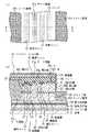
Next, a second embodiment will be described. FIG. 5A is a plan view showing the positional relationship of electrodes and the like of the semiconductor device according to the second embodiment, and FIG. 5B is a cross section showing the structure of the semiconductor device according to the second embodiment. FIG. FIG.5 (b) has shown the cross section along the II-II line | wire in Fig.5 (a).
図5(a)及び(b)に示すように、第2の実施形態では、基板21上に、バッファ層22、電子走行層23、電子供給層24、キャップ層25、絶縁層26、及びn型GaN層27がこの順で形成されている。基板21、バッファ層22、電子走行層23、電子供給層24、キャップ層25、絶縁層26としては、夫々、基板1、バッファ層2、電子走行層3、電子供給層4、キャップ層5、絶縁層6と同様のものが用いられる。n型GaN層27の厚さは、例えば10nm〜5000nmである。 As shown in FIGS. 5A and 5B, in the second embodiment, the
n型GaN層27、及び絶縁層26には、キャップ層25の厚さ方向の一部まで入り込むゲート電極用の開口部30gが形成されている。また、n型GaN層27、絶縁層26、及びキャップ層25には、平面視で開口部30gを間に挟むようにして、ソース電極用の開口部30s及びドレイン電極用の開口部30dが形成されている。そして、開口部30g内にゲート電極31gが形成され、開口部30s内にソース電極31sが形成され、開口部30d内にドレイン電極31dが形成されている。例えば、ゲート電極31g及びソース電極31sの上面は、n型GaN層27の上面よりも高い位置にあり、ドレイン電極31dの上面は、絶縁層26の上面とキャップ層25の上面との間に位置する。 In the n-
ゲート電極31gよりもドレイン電極31d側では、ゲート電極31g及びドレイン電極31d間の領域を二分する信号ライン33が、絶縁膜39を介してn型GaN層27上に形成されている。そして、平面視で、信号ライン33とゲート電極31gとの間、及び信号ライン33とドレイン電極31dとの間の領域では、n型GaN層27の表層部にp型不純物が導入されてp型GaN層41が形成されている。また、信号ライン33よりもドレイン電極31d側では、信号ライン33及びドレイン電極31d間の領域を二分するパッド34がp型GaN層41上に形成されている。 A
ゲート電極31gよりもソース電極31s側では、n型GaN層27の表層部にp型不純物が導入されてp型GaN層41が形成されている。また、ゲート電極31g及びソース電極31s間の領域を二分する信号ライン32が、絶縁膜38を介してp型GaN層41上に形成されている。そして、平面視で、信号ライン32とゲート電極31gとの間、及び信号ライン32とソース電極31sとの間の領域では、p型GaN層41の表層部にn型不純物が導入されてn型GaN層42が形成されている。 A p-type impurity is introduced into the surface layer portion of the n-
ゲート電極31g、ソース電極31s、信号ライン32、信号ライン33、及びパッド34を覆う絶縁層29が形成されている。絶縁層29としては、絶縁層9と同様のものが用いられる。絶縁層29には、パッド34まで到達する孔35a及びこの孔35aに連通する溝35bが形成されており、孔35a内及び溝35b内に電源ライン36が埋め込まれている。 An insulating
絶縁層29、電源ライン36、及びドレイン電極31dを覆うパッシベーション膜37が形成されている。パッシベーション膜37に、電源ライン36の一部を露出する開口部、及びドレイン電極31dの一部を露出する開口部が形成されている。パッシベーション膜37及び絶縁層29に、ソース電極31sの一部を露出する開口部が形成されている。これらの開口部を介して、第1の実施形態と同様に、電源ライン36が外部端子51に接続され、ソース電極31sが外部端子52に接続され、ドレイン電極31dが外部端子53に接続される。また、信号ライン32及び33は、基板21上に形成されたゲートドライバに接続される。例えば、このゲートドライバもパッシベーション膜37に覆われる。 A passivation film 37 is formed to cover the insulating
このように構成された半導体装置には、ゲート電極31g、ソース電極31s及びドレイン電極31dを備えたGaN系のHEMTが含まれる。そして、例えば、ソース電極31sは外部端子52を介して接地され、電源ライン36は外部端子51を介して12Vの電源に接続され、ドレイン電極31dには外部端子53を介してHEMTの用途に応じた所定の電圧が供給される。また、ゲートドライバから、信号ライン32に0V又は12Vの電圧が印加され、信号ライン33に24V又は0Vの電圧が印加される。従って、ゲート電極31gには、信号ライン32に印加される電圧及び信号ライン33に印加される電圧に応じた電圧が印加され、この電圧に応じてHEMTのオン/オフが切り替えられる。即ち、HEMTのオン/オフの切り替えは、第1の実施形態と同様に、表1に示す電圧制御により行われる。そして、この電圧制御の際には、基板21上に形成されたゲートドライバから信号ライン32及び33に電圧が印加され、n型GaN層27又はp型GaN層41を電荷が高速で移動する。従って、Si系トランジスタを用いてHEMTのゲート電圧を印加する場合と比較して、HEMTをより高速に動作させることが可能である。 The semiconductor device thus configured includes a GaN-based HEMT including a
次に、第2の実施形態に係る半導体装置を製造する方法について説明する。図6A乃至図6Cは、第2の実施形態に係る半導体装置の製造方法を工程順に示す断面図である。 Next, a method for manufacturing the semiconductor device according to the second embodiment will be described. 6A to 6C are cross-sectional views illustrating the method of manufacturing the semiconductor device according to the second embodiment in the order of steps.
先ず、図6A(a)に示すように、基板21上に、例えばMOCVD法により、バッファ層22、電子走行層23、電子供給層24、キャップ層25、絶縁層26、及びn型GaN層27をこの順で形成する。 First, as shown in FIG. 6A (a), a
バッファ層22、電子走行層23、電子供給層24、キャップ層25、絶縁層26を形成する際の条件は、バッファ層2、電子走行層3、電子供給層4、キャップ層5、絶縁層6を形成する際の条件と同様である。n型GaN層27を形成する場合の条件は、例えば、以下のように設定する。
トリメチルガリウム(TMG)の流量:1〜50sccm、
アンモニア(NH3)の流量:10〜10000sccm、
n型不純物:シラン(SiH4)、
圧力:100Torr、
温度:1100℃。The conditions for forming the
Trimethylgallium (TMG) flow rate: 1-50 sccm,
Ammonia (NH3 ) flow rate: 10-10000 sccm,
n-type impurity: silane (SiH4 ),
Pressure: 100 Torr,
Temperature: 1100 ° C.
次いで、図6A(b)に示すように、n型GaN層27上に信号ライン33を形成する。信号ライン33は、例えばリフトオフ法により形成する。その後、信号ライン33をマスクとして用いてn型GaN層27にp型不純物(例えば、Mg)をドーピングすることにより、n型GaN層27の表面にp型GaN層41を形成する。 Next, as shown in FIG. 6A (b), a
続いて、図6B(c)に示すように、ゲート電極用の開口部30g、ソース電極用の開口部30s及びドレイン電極用の開口部30dを形成する。開口部30g、開口部30s、及び開口部30dは、開口部10g、開口部10s、及び開口部10dと同様にして形成することができる。 Subsequently, as shown in FIG. 6B (c), an
次いで、図6B(d)に示すように、ゲート電極31gを形成し、ソース電極31s及びドレイン電極31dを形成し、信号ライン32を形成し、パッド34を形成する。これらの形成順序は特に限定されない。これらは、例えばリフトオフ法により形成することができる。 Next, as shown in FIG. 6B (d), a
その後、図6C(e)に示すように、ゲート電極31gとソース電極31sとの間の領域において、信号ライン32をマスクとして用いてp型GaN層41にn型不純物(例えば、Si)をドーピングすることにより、p型GaN層41の表面にn型GaN層42を形成する。この際、ゲート電極31gとドレイン電極31dとの間の領域は、レジストパターン等により覆っておく。 Thereafter, as shown in FIG. 6C (e), in the region between the
そして、図6C(f)に示すように、絶縁層29の形成、溝35b及び孔35aの形成、電源ライン36の形成、及びパッシベーション膜37の形成等を行う。これらの処理は、第1の実施形態と同様にして行えばよい。 Then, as shown in FIG. 6C (f), the insulating
このようにして半導体装置を完成させることができる。 In this way, the semiconductor device can be completed.
なお、第2の実施形態では、ゲート電極31gとして、図7に示すように、平面視で、ソース電極31s側に位置するソース側部31gs及びドレイン電極31d側に位置するドレイン側部31gdを備えたものを用いることが好ましい。ゲート電極31gとソース電極31sとの間にはnpn接合が存在し、ゲート電極31gとドレイン電極31dとの間にはpnp接合が存在するため、ゲート電極31gの材料をこれらの接合の種類に応じて選択できるようにするためである。 In the second embodiment, as shown in FIG. 7, the
ゲート電極31g、ソース電極31s、ドレイン電極31d、信号ライン32、信号ライン33、及びパッド34の材料は特に限定されない。信号ライン32の材料としては、例えば、多結晶シリコン、Ni、Cr、Ti、Al等が挙げられる。また、これらの材料の膜の積層体を用いてもよい。信号ライン33の材料としては、例えば、多結晶シリコン、Ni、TiAlN等が挙げられる。また、これらの材料の膜の積層体を用いてもよい。ゲート電極31gのソース側部31gsの材料としては、例えば、Al、Ta等が挙げられる。また、ソース側部31gsとして、Ta膜及びその上に形成されたAl膜の積層体を用いてもよい。ゲート電極31gのドレイン側部31gdの材料としては、例えば、Pd、Au等が挙げられる。また、ドレイン側部31gdとして、Pd膜及びその上に形成されたAu膜の積層体を用いてもよい。パッド34の材料としては、例えば、Pd、Au等が挙げられる。また、パッド34として、Pd膜及びその上に形成されたAu膜の積層体を用いてもよい。ソース電極31s及びドレイン電極31dの材料としては、例えば、Al、Ta等が挙げられる。また、ソース電極31s及びドレイン電極31dとして、Ta膜及びその上に形成されたAl膜の積層体を用いてもよい。 The materials of the
(第3の実施形態)
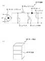
次に、第3の実施形態について説明する。第3の実施形態は、第1又は第2の実施形態に係る半導体装置を備えたサーバ電源等の装置である。図8(a)は、PFC(power factor correction)回路を示す図であり、図8(b)は、図8(a)に示すPFC回路を含むサーバ電源を示す図である。(Third embodiment)
Next, a third embodiment will be described. The third embodiment is an apparatus such as a server power supply including the semiconductor device according to the first or second embodiment. FIG. 8A is a diagram showing a PFC (power factor correction) circuit, and FIG. 8B is a diagram showing a server power supply including the PFC circuit shown in FIG. 8A.
図8(a)に示すように、PFC回路には、交流電源(AC)が接続されるダイオードブリッジ91に接続されたコンデンサ92が設けられている。コンデンサ92の一端子にはチョークコイル93の一端子が接続され、チョークコイル93の他端子には、スイッチ素子94の一端子及びダイオード96のアノードが接続されている。スイッチ素子94は第1又は第2の実施形態におけるHEMTに相当し、当該一端子は第1又は第2の実施形態におけるドレイン電極11d又は31dに相当する。また、スイッチ素子94の他端子は第1又は第2の実施形態におけるソース電極11s又は31sに相当する。スイッチ素子94のオン/オフが、基板1又は21上に形成されたゲートドライバにより制御される。ダイオード96のカソードにはコンデンサ95の一端子が接続されている。コンデンサ92の他端子、スイッチ素子94の当該他端子、及びコンデンサ95の他端子が接地される。そして、コンデンサ95の両端子間から直流電源(DC)が取り出される。 As shown in FIG. 8A, the PFC circuit is provided with a capacitor 92 connected to a diode bridge 91 to which an AC power supply (AC) is connected. One terminal of the capacitor 92 is connected to one terminal of the choke coil 93, and the other terminal of the choke coil 93 is connected to one terminal of the switch element 94 and the anode of the diode 96. The switch element 94 corresponds to the HEMT in the first or second embodiment, and the one terminal corresponds to the
そして、図8(b)に示すように、PFC回路90は、サーバ電源100等に組み込まれて用いられる。 Then, as shown in FIG. 8B, the PFC circuit 90 is used by being incorporated in the server power supply 100 or the like.
このようなサーバ電源100と同様の、より高速動作が可能な電源装置を構築することも可能である。また、スイッチ素子94と同様のスイッチ素子は、スイッチ電源又は電子機器に用いることができる。更に、これらの半導体装置を、サーバの電源回路等のフルブリッジ電源回路用の部品として用いることも可能である。また、これらの半導体装置は、パワーアンプ等高周波用途の電子機器に用いることができる。また、これらの半導体装置は、集積回路として用いることができる。 It is also possible to construct a power supply device that can operate at a higher speed, similar to the server power supply 100. A switch element similar to the switch element 94 can be used for a switch power supply or an electronic device. Further, these semiconductor devices can be used as components for a full-bridge power supply circuit such as a server power supply circuit. In addition, these semiconductor devices can be used for high-frequency electronic devices such as power amplifiers. In addition, these semiconductor devices can be used as integrated circuits.
以下、本発明の諸態様を付記としてまとめて記載する。 Hereinafter, various aspects of the present invention will be collectively described as supplementary notes.
(付記1)
基板と、
前記基板の上方に形成された電子走行層及び電子供給層を備えたトランジスタと、
前記基板の上方に形成され、前記トランジスタのゲートに接続された窒化物半導体層と、
前記窒化物半導体層を移動する電荷を制御する制御手段と、
を有することを特徴とする半導体装置。(Appendix 1)
A substrate,
A transistor having an electron transit layer and an electron supply layer formed above the substrate;
A nitride semiconductor layer formed above the substrate and connected to a gate of the transistor;
Control means for controlling the charge moving through the nitride semiconductor layer;
A semiconductor device comprising:
(付記2)
前記電子供給層と前記窒化物半導体層との間に形成されたn型GaN層を有することを特徴とする付記1に記載の半導体装置。(Appendix 2)
The semiconductor device according to
(付記3)
前記トランジスタと前記窒化物半導体層とを絶縁する絶縁層を有することを特徴とする付記1又は2に記載の半導体装置。(Appendix 3)
The semiconductor device according to
(付記4)
前記絶縁層は、AlN層、AlGaN層、p型GaN層、FeドープGaN層、Si酸化物層、Al酸化物層、Si窒化物層、及びC層からなる群から選択された少なくとも1種を含むことを特徴とする付記3に記載の半導体装置。(Appendix 4)
The insulating layer includes at least one selected from the group consisting of an AlN layer, an AlGaN layer, a p-type GaN layer, an Fe-doped GaN layer, a Si oxide layer, an Al oxide layer, a Si nitride layer, and a C layer. The semiconductor device according to attachment 3, wherein the semiconductor device is included.
(付記5)
前記制御手段は、前記窒化物半導体層上に形成された信号ラインを有することを特徴とする付記1乃至4のいずれか1項に記載の半導体装置。(Appendix 5)
The semiconductor device according to any one of
(付記6)
前記制御手段は、前記基板上に形成され、前記信号ラインを駆動するゲートドライバを有することを特徴とする付記5に記載の半導体装置。(Appendix 6)
6. The semiconductor device according to
(付記7)
前記窒化物半導体層に接続された第1の外部端子と、
前記窒化物半導体層の前記第1の外部端子に接続された部分とは前記ゲートの逆側に位置する部分に接続され、前記第1の外部端子よりも高い電圧が供給される第2の外部端子と、
を有し、
前記制御手段は、
前記第1の外部端子と前記ゲートとの間で前記窒化物半導体層の電位を制御する第1の信号ラインと、
前記第2の外部端子と前記ゲートとの間で前記窒化物半導体層の電位を制御する第2の信号ラインと、
を有することを特徴とする付記1乃至4のいずれか1項に記載の半導体装置。(Appendix 7)
A first external terminal connected to the nitride semiconductor layer;
A portion of the nitride semiconductor layer connected to the portion connected to the first external terminal and connected to a portion located on the opposite side of the gate, and supplied with a voltage higher than that of the first external terminal. A terminal,
Have
The control means includes
A first signal line for controlling a potential of the nitride semiconductor layer between the first external terminal and the gate;
A second signal line for controlling the potential of the nitride semiconductor layer between the second external terminal and the gate;
5. The semiconductor device according to any one of
(付記8)
前記制御手段は、前記基板上に形成され、前記第1の信号ライン及び前記第2の信号ラインを駆動するゲートドライバを有することを特徴とする付記7に記載の半導体装置。(Appendix 8)
8. The semiconductor device according to
(付記9)
前記窒化物半導体層は、互いに積層された第2の電子走行層及び第2の電子供給層を有することを特徴とする付記1乃至8のいずれか1項に記載の半導体装置。(Appendix 9)
9. The semiconductor device according to any one of
(付記10)
前記第2の電子走行層はGaN層を有し、
前記第2の電子供給層はAlGaN層を有することを特徴とする付記9に記載の半導体装置。(Appendix 10)
The second electron transit layer has a GaN layer;
The semiconductor device according to
(付記11)
前記窒化物半導体層は、前記電荷の移動方向に並んだ、第1導電型の第1領域、第2導電型の第2領域、及び第1導電型の第3領域を有し、
前記信号ラインは、前記第2領域上に位置することを特徴とする付記5又は6に記載の半導体装置。(Appendix 11)
The nitride semiconductor layer has a first conductivity type first region, a second conductivity type second region, and a first conductivity type third region arranged in the direction of movement of the charge,
The semiconductor device according to
(付記12)
前記窒化物半導体層の前記第1の外部端子に接続された部分は、前記電荷の移動方向に並んだ、第1導電型の第1領域、第2導電型の第2領域、及び第1導電型の第3領域を有し、
前記第1の信号ラインは、前記第2領域上に位置し、
前記窒化物半導体層の前記第2の外部端子に接続された部分は、前記電荷の移動方向に並んだ、第2導電型の第4領域、第1導電型の第5領域、及び第2導電型の第6領域を有し、
前記第2の信号ラインは、前記第5領域上に位置することを特徴とする付記7又は8に記載の半導体装置。(Appendix 12)
A portion of the nitride semiconductor layer connected to the first external terminal is arranged in the charge movement direction, the first conductivity type first region, the second conductivity type second region, and the first conductivity type. A third region of the mold,
The first signal line is located on the second region;
Portions of the nitride semiconductor layer connected to the second external terminal are arranged in the direction of charge movement, the second conductivity type fourth region, the first conductivity type fifth region, and the second conductivity type. Having a sixth region of the mold,
9. The semiconductor device according to
(付記13)
基板の上方に、電子走行層及び電子供給層を備えたトランジスタを形成する工程と、
前記基板の上方に、前記トランジスタのゲートに接続される窒化物半導体層を形成する工程と、
前記窒化物半導体層を移動する電荷を制御する制御手段を形成する工程と、
を有することを特徴とする半導体装置の製造方法。(Appendix 13)
Forming a transistor having an electron transit layer and an electron supply layer above the substrate;
Forming a nitride semiconductor layer connected to the gate of the transistor above the substrate;
Forming a control means for controlling the charge moving through the nitride semiconductor layer;
A method for manufacturing a semiconductor device, comprising:
(付記14)
前記トランジスタを形成する工程と前記窒化物半導体層を形成する工程との間に、前記電子供給層上にn型GaN層を形成する工程を有し、
前記窒化物半導体層を前記n型GaN層上に形成することを特徴とする付記13に記載の半導体装置の製造方法。(Appendix 14)
A step of forming an n-type GaN layer on the electron supply layer between the step of forming the transistor and the step of forming the nitride semiconductor layer;
14. The method for manufacturing a semiconductor device according to
(付記15)
前記トランジスタと前記窒化物半導体層とを絶縁する絶縁層を形成する工程を有することを特徴とする付記13又は14に記載の半導体装置の製造方法。(Appendix 15)
15. The method of manufacturing a semiconductor device according to
(付記16)
前記制御手段を形成する工程は、前記窒化物半導体層上に信号ラインを形成する工程を有することを特徴とする付記13乃至15のいずれか1項に記載の半導体装置の製造方法。(Appendix 16)
16. The method of manufacturing a semiconductor device according to any one of
(付記17)
前記制御手段を形成する工程は、
前記窒化物半導体層に接続される第1の外部端子と前記ゲートとの間で前記窒化物半導体層の電位を制御する第1の信号ラインを形成する工程と、
前記窒化物半導体層の前記第1の外部端子に接続された部分とは前記ゲートの逆側に位置する部分に接続され、前記第1の外部端子よりも高い電圧が供給される第2の外部端子と前記ゲートとの間で前記窒化物半導体層の電位を制御する第2の信号ラインを形成する工程と、
を有することを特徴とする付記13乃至15のいずれか1項に記載の半導体装置の製造方法。(Appendix 17)
The step of forming the control means includes
Forming a first signal line for controlling a potential of the nitride semiconductor layer between a first external terminal connected to the nitride semiconductor layer and the gate;
A portion of the nitride semiconductor layer connected to the portion connected to the first external terminal and connected to a portion located on the opposite side of the gate, and supplied with a voltage higher than that of the first external terminal. Forming a second signal line for controlling a potential of the nitride semiconductor layer between a terminal and the gate;
16. The method for manufacturing a semiconductor device according to any one of
(付記18)
前記窒化物半導体層を形成する工程は、互いに積層される第2の電子走行層及び第2の電子供給層を形成する工程を有することを特徴とする付記13乃至17のいずれか1項に記載の半導体装置の製造方法。(Appendix 18)
18. The method according to any one of
(付記19)
前記第2の電子走行層としてGaN層を形成し、
前記第2の電子供給層としてAlGaN層を形成することを特徴とする付記18に記載の半導体装置の製造方法。(Appendix 19)
Forming a GaN layer as the second electron transit layer;
19. The method of manufacturing a semiconductor device according to
(付記20)
付記1乃至12のいずれか1項に記載の半導体装置を有することを特徴とする電源装置。(Appendix 20)
A power supply device comprising the semiconductor device according to any one of
1、21:基板
2、22:バッファ層
3、23:電子走行層
4、24:電子供給層
5、25:キャップ層
6、26:絶縁層
7:電子走行層
8:電子供給層
11g:ゲート電極
11s:ソース電極
11d:ドレイン電極
12、13、32、33:信号ライン
16、36:電源ライン
27、42:n型GaN層
41:p型GaN層DESCRIPTION OF
Claims (6)
Translated fromJapanese前記基板の上方に形成された、ゲート電極、電子走行層及び電子供給層を備えたトランジスタと、
前記電子供給層上方に形成された絶縁層と、
前記絶縁層の上方に形成された窒化物半導体層と、
前記窒化物半導体層上方に、平面視で前記ゲート電極を間に挟むようにして形成された第1の電極及び第2の電極と、
前記窒化物半導体層上方で、かつ平面視で前記ゲート電極と前記第1の電極との間に形成された第1の信号ラインと、
前記窒化物半導体層上方で、かつ平面視で前記ゲート電極と前記第2の電極との間に形成された第2の信号ラインと、
を有し、
前記ゲート電極は、前記絶縁層より上方に位置して前記窒化物半導体層と接する部分を有し、
前記第1の信号ラインは、前記ゲート電極と前記第1の電極との間で前記窒化物半導体層を移動する電荷を制御し、
前記第2の信号ラインは、前記ゲート電極と前記第2の電極との間で前記窒化物半導体層を移動する電荷を制御することを特徴とする半導体装置。A substrate,
A transistor including a gate electrode, an electron transit layer, and an electron supply layer formed above the substrate;
An insulating layer formed above the electron supply layer;
A nitride semiconductor layer formed above the insulating layer;
A first electrode and a second electrode formed above the nitride semiconductor layer so as to sandwich the gate electrode in plan view;
A first signal line formed above the nitride semiconductor layer and between the gate electrode and the first electrode in plan view;
A second signal line formed above the nitride semiconductor layer and between the gate electrode and the second electrode in plan view;
Have
It said gate electrode is positioned above said insulating layerhave a portion in contact with the nitride semiconductorlayer,
The first signal line controls a charge moving through the nitride semiconductor layer between the gate electrode and the first electrode;
The semiconductor device, wherein the second signal line controls acharge that moves in the nitride semiconductor layer between the gate electrode and the second electrode .
前記第2の電子供給層はAlGaN層を有することを特徴とする請求項3に記載の半導体装置。The second electron transit layer has a GaN layer;
The semiconductor device according to claim 3, wherein the second electron supply layer includes an AlGaN layer.
前記第1の信号ラインは、前記第2領域上に位置し、
前記窒化物半導体層の前記ゲート電極と前記第2の電極との間の部分は、前記電荷の移動方向に並んだ、第2導電型の第4領域、第1導電型の第5領域、及び第2導電型の第6領域を有し、
前記第2の信号ラインは、前記第5領域上に位置することを特徴とする請求項1又は2に記載の半導体装置。A portion of the nitride semiconductor layer between the gate electrode and the first electrode is arranged in the charge movement direction, the first conductivity type first region, the second conductivity type second region, and Having a third region of the first conductivity type;
The first signal line is located on the second region;
A portion of the nitride semiconductor layer between the gate electrode and the second electrode is arranged in a direction in which the electric charge moves, a second conductivity type fourth region, a first conductivity type fifth region, and Having a sixth region of the second conductivity type;
The semiconductor device according to claim 1, wherein the second signal line is located on the fifth region.
前記電子供給層上方に絶縁層を形成する工程と、
前記絶縁層の上方に窒化物半導体層を形成する工程と、
前記窒化物半導体層上方に、平面視で前記ゲート電極を間に挟むようにして第1の電極及び第2の電極を形成する工程と、
前記窒化物半導体層上方で、かつ平面視で前記ゲート電極と前記第1の電極との間に第1の信号ラインを形成する工程と、
前記窒化物半導体層上方で、かつ平面視で前記ゲート電極と前記第2の電極との間に第2の信号ラインを形成する工程と、
を有し、
前記ゲート電極は、前記絶縁層より上方に位置して前記窒化物半導体層と接する部分を有し、
前記第1の信号ラインは、前記ゲート電極と前記第1の電極との間で前記窒化物半導体層を移動する電荷を制御し、
前記第2の信号ラインは、前記ゲート電極と前記第2の電極との間で前記窒化物半導体層を移動する電荷を制御することを特徴とする半導体装置の製造方法。Forming a transistor having a gate electrode, an electron transit layer, and an electron supply layer above the substrate;
Forming an insulating layer above the electron supply layer;
Forming a nitride semiconductor layer above the insulating layer;
Forming a first electrode and a second electrode above the nitride semiconductor layer so as to sandwich the gate electrode in plan view;
Forming a first signalline above the nitride semiconductor layer and between the gate electrode and the first electrode in plan view;
Forming a second signalline above the nitride semiconductor layer and between the gate electrode and the second electrode in plan view;
Have
It said gate electrode is positioned above said insulating layerhave a portion in contact with the nitride semiconductorlayer,
The first signal line controls a charge moving through the nitride semiconductor layer between the gate electrode and the first electrode;
The method of manufacturing a semiconductor device,wherein the second signal line controls acharge moving through the nitride semiconductor layer between the gate electrode and the second electrode .
Priority Applications (5)
| Application Number | Priority Date | Filing Date | Title |
|---|---|---|---|
| JP2010246743AJP5845568B2 (en) | 2010-11-02 | 2010-11-02 | Semiconductor device and manufacturing method thereof |
| US13/208,779US8941116B2 (en) | 2010-11-02 | 2011-08-12 | Semiconductor device and method of manufacturing the same |
| TW100129763ATWI441332B (en) | 2010-11-02 | 2011-08-19 | Semiconductor device and method of manufacturing same |
| CN201110259610.XACN102468331B (en) | 2010-11-02 | 2011-08-30 | Semiconductor device and manufacture method thereof |
| KR1020110087398AKR101264528B1 (en) | 2010-11-02 | 2011-08-30 | Semiconductor device and method of manufacturing the same |
Applications Claiming Priority (1)
| Application Number | Priority Date | Filing Date | Title |
|---|---|---|---|
| JP2010246743AJP5845568B2 (en) | 2010-11-02 | 2010-11-02 | Semiconductor device and manufacturing method thereof |
Publications (2)
| Publication Number | Publication Date |
|---|---|
| JP2012099674A JP2012099674A (en) | 2012-05-24 |
| JP5845568B2true JP5845568B2 (en) | 2016-01-20 |
Family
ID=45995683
Family Applications (1)
| Application Number | Title | Priority Date | Filing Date |
|---|---|---|---|
| JP2010246743AExpired - Fee RelatedJP5845568B2 (en) | 2010-11-02 | 2010-11-02 | Semiconductor device and manufacturing method thereof |
Country Status (5)
| Country | Link |
|---|---|
| US (1) | US8941116B2 (en) |
| JP (1) | JP5845568B2 (en) |
| KR (1) | KR101264528B1 (en) |
| CN (1) | CN102468331B (en) |
| TW (1) | TWI441332B (en) |
Families Citing this family (8)
| Publication number | Priority date | Publication date | Assignee | Title |
|---|---|---|---|---|
| US9773877B2 (en) | 2004-05-13 | 2017-09-26 | Cree, Inc. | Wide bandgap field effect transistors with source connected field plates |
| US11791385B2 (en) | 2005-03-11 | 2023-10-17 | Wolfspeed, Inc. | Wide bandgap transistors with gate-source field plates |
| WO2011161791A1 (en)* | 2010-06-24 | 2011-12-29 | 富士通株式会社 | Semiconductor device |
| ES2743052T3 (en)* | 2013-04-09 | 2020-02-18 | Otis Elevator Co | Drive unit architecture employing gallium nitride switches |
| US9679981B2 (en) | 2013-06-09 | 2017-06-13 | Cree, Inc. | Cascode structures for GaN HEMTs |
| US9755059B2 (en)* | 2013-06-09 | 2017-09-05 | Cree, Inc. | Cascode structures with GaN cap layers |
| US9847411B2 (en) | 2013-06-09 | 2017-12-19 | Cree, Inc. | Recessed field plate transistor structures |
| US20180061975A1 (en)* | 2016-08-24 | 2018-03-01 | Rohm Co., Ltd. | Nitride semiconductor device and nitride semiconductor package |
Family Cites Families (34)
| Publication number | Priority date | Publication date | Assignee | Title |
|---|---|---|---|---|
| JPH0680793B2 (en)* | 1985-06-28 | 1994-10-12 | 日本電気株式会社 | Three-dimensional integrated circuit |
| US7079275B2 (en) | 2000-03-28 | 2006-07-18 | Mongonet | Method and system for facilitating paper to electronic communications |
| US7940411B2 (en) | 2000-03-28 | 2011-05-10 | Mongonet | Method and system for entry of electronic data via fax-to-email communication |
| US8275100B2 (en) | 2000-03-28 | 2012-09-25 | Mongonet | Methods and apparatus for billing of facsimile transmissions to electronic storage destinations |
| US8045203B2 (en) | 2000-03-28 | 2011-10-25 | Mongonet | Methods and apparatus for secure facsimile transmissions to electronic storage destinations |
| US7944573B2 (en) | 2000-03-28 | 2011-05-17 | Mongonet | Methods and apparatus for authenticating facsimile transmissions to electronic storage destinations |
| US8035834B2 (en) | 2000-03-28 | 2011-10-11 | Mongonet | Methods and apparatus for manipulating and providing facsimile transmissions to electronic storage destinations |
| US8023132B2 (en) | 2000-03-28 | 2011-09-20 | Mongonet | Method and system for transferring digitized representations of documents via computer network transfer protocols |
| US8184318B2 (en) | 2000-03-28 | 2012-05-22 | Mongonet | Methods and apparatus for compositing facsimile transmissions to electronic storage destinations |
| JP5130641B2 (en) | 2006-03-31 | 2013-01-30 | サンケン電気株式会社 | Composite semiconductor device |
| US6424426B1 (en) | 2000-03-28 | 2002-07-23 | Mongonet | Fax-to-email and email-to-fax communication system and method |
| US7817295B2 (en) | 2000-03-28 | 2010-10-19 | Mongonet | Method and system for modified document transfer via computer network transfer protocols |
| US7755790B2 (en) | 2000-03-28 | 2010-07-13 | Mongonet | Method and system for transferring sponsored digitized representations of documents via computer network transfer protocols |
| US7746496B2 (en) | 2000-03-28 | 2010-06-29 | Mongonet | Method and system for pay per use document transfer via computer network transfer protocols |
| US8045204B2 (en) | 2000-03-28 | 2011-10-25 | Mongonet | Methods and apparatus for facsimile transmissions to electronic storage destinations including tracking data |
| US8023131B2 (en) | 2000-03-28 | 2011-09-20 | Mongonet | Method and system for combining separate digitized representations of documents for retransmission via computer network transfer protocols |
| US20070236750A1 (en) | 2000-03-28 | 2007-10-11 | Mongonet | Methods and apparatus for facilitating facsimile transmissions to electronic storage destinations |
| US7826100B2 (en) | 2000-03-28 | 2010-11-02 | Mongonet | Methods and apparatus for facsimile transmissions to electronic storage destinations including embedded barcode fonts |
| US20090059271A1 (en) | 2000-03-28 | 2009-03-05 | Mongonet | Methods and apparatus for web-based status of facsimile transmissions to electronic storage destinations |
| US6479844B2 (en) | 2001-03-02 | 2002-11-12 | University Of Connecticut | Modulation doped thyristor and complementary transistor combination for a monolithic optoelectronic integrated circuit |
| JP2003289082A (en)* | 2002-03-28 | 2003-10-10 | Matsushita Electric Ind Co Ltd | Semiconductor device for communication equipment and equipment for communication system |
| JP4077731B2 (en) | 2003-01-27 | 2008-04-23 | 富士通株式会社 | Compound semiconductor device and manufacturing method thereof |
| US11791385B2 (en) | 2005-03-11 | 2023-10-17 | Wolfspeed, Inc. | Wide bandgap transistors with gate-source field plates |
| US20080166173A1 (en) | 2007-01-05 | 2008-07-10 | Kevin Augustine Gibbons | Mobile marking board implement holder |
| JP2008198675A (en)* | 2007-02-09 | 2008-08-28 | Doshisha | Stacked semiconductor integrated device |
| JP5417693B2 (en) | 2007-08-22 | 2014-02-19 | 日本電気株式会社 | Semiconductor device |
| US7859021B2 (en)* | 2007-08-29 | 2010-12-28 | Sanken Electric Co., Ltd. | Field-effect semiconductor device |
| JP5369434B2 (en)* | 2007-12-21 | 2013-12-18 | サンケン電気株式会社 | Bidirectional switch |
| JP2009158528A (en)* | 2007-12-25 | 2009-07-16 | Sharp Corp | Semiconductor device |
| JP5439725B2 (en)* | 2008-02-20 | 2014-03-12 | サンケン電気株式会社 | Semiconductor switching device |
| JP5338433B2 (en)* | 2008-09-30 | 2013-11-13 | 富士電機株式会社 | Gallium nitride semiconductor device and manufacturing method thereof |
| JP5533661B2 (en)* | 2008-10-29 | 2014-06-25 | 富士通株式会社 | Compound semiconductor device and manufacturing method thereof |
| JP2010135640A (en)* | 2008-12-05 | 2010-06-17 | Panasonic Corp | Field-effect transistor |
| JP5564791B2 (en)* | 2008-12-26 | 2014-08-06 | 富士通株式会社 | Compound semiconductor device and manufacturing method thereof |
- 2010
- 2010-11-02JPJP2010246743Apatent/JP5845568B2/ennot_activeExpired - Fee Related
- 2011
- 2011-08-12USUS13/208,779patent/US8941116B2/ennot_activeExpired - Fee Related
- 2011-08-19TWTW100129763Apatent/TWI441332B/ennot_activeIP Right Cessation
- 2011-08-30CNCN201110259610.XApatent/CN102468331B/ennot_activeExpired - Fee Related
- 2011-08-30KRKR1020110087398Apatent/KR101264528B1/ennot_activeExpired - Fee Related
Also Published As
| Publication number | Publication date |
|---|---|
| TWI441332B (en) | 2014-06-11 |
| JP2012099674A (en) | 2012-05-24 |
| CN102468331B (en) | 2016-07-06 |
| US8941116B2 (en) | 2015-01-27 |
| US20120104408A1 (en) | 2012-05-03 |
| CN102468331A (en) | 2012-05-23 |
| KR20120046675A (en) | 2012-05-10 |
| KR101264528B1 (en) | 2013-05-14 |
| TW201238048A (en) | 2012-09-16 |
Similar Documents
| Publication | Publication Date | Title |
|---|---|---|
| JP5845568B2 (en) | Semiconductor device and manufacturing method thereof | |
| JP5810518B2 (en) | Compound semiconductor device and manufacturing method thereof | |
| TWI770134B (en) | Semiconductor device and manufacturing method of semiconductor device | |
| TWI470795B (en) | Semiconductor device and method of manufacturing the same | |
| JP5573941B2 (en) | Compound semiconductor device and manufacturing method thereof | |
| JP6018360B2 (en) | Compound semiconductor device and manufacturing method thereof | |
| JP5950643B2 (en) | Compound semiconductor device and manufacturing method thereof | |
| JP5902010B2 (en) | Compound semiconductor device and manufacturing method thereof | |
| JP4956155B2 (en) | Semiconductor electronic device | |
| WO2008035403A1 (en) | Field-effect transistor | |
| JP2008166469A (en) | Nitride semiconductor device and manufacturing method thereof | |
| JP2010258441A (en) | Field effect transistor | |
| KR101357526B1 (en) | Semiconductor device and method of manufacturing the same | |
| JP2013207245A (en) | Compound semiconductor device and method of manufacturing the same | |
| CN103855207A (en) | Compound semiconductor device and manufacturing method of the same | |
| JP5741042B2 (en) | Compound semiconductor device and manufacturing method thereof | |
| JP5510544B2 (en) | Compound semiconductor device and manufacturing method thereof | |
| JP7009952B2 (en) | Semiconductor devices and methods for manufacturing semiconductor devices | |
| JP2017085003A (en) | Semiconductor device and manufacturing method thereof, power supply device, and high-frequency amplifier | |
| JP5128060B2 (en) | Semiconductor device and method for manufacturing semiconductor device | |
| JP2014197644A (en) | Compound semiconductor device and method of manufacturing the same | |
| CN103430294B (en) | Compound semiconductor device and manufacturing method thereof | |
| JP6187167B2 (en) | Compound semiconductor device and manufacturing method thereof | |
| US20160005848A1 (en) | Semiconductor device |
Legal Events
| Date | Code | Title | Description |
|---|---|---|---|
| A621 | Written request for application examination | Free format text:JAPANESE INTERMEDIATE CODE: A621 Effective date:20130805 | |
| A977 | Report on retrieval | Free format text:JAPANESE INTERMEDIATE CODE: A971007 Effective date:20140924 | |
| A131 | Notification of reasons for refusal | Free format text:JAPANESE INTERMEDIATE CODE: A131 Effective date:20140930 | |
| A521 | Request for written amendment filed | Free format text:JAPANESE INTERMEDIATE CODE: A523 Effective date:20141201 | |
| A131 | Notification of reasons for refusal | Free format text:JAPANESE INTERMEDIATE CODE: A131 Effective date:20150804 | |
| A521 | Request for written amendment filed | Free format text:JAPANESE INTERMEDIATE CODE: A523 Effective date:20151005 | |
| TRDD | Decision of grant or rejection written | ||
| A01 | Written decision to grant a patent or to grant a registration (utility model) | Free format text:JAPANESE INTERMEDIATE CODE: A01 Effective date:20151027 | |
| A61 | First payment of annual fees (during grant procedure) | Free format text:JAPANESE INTERMEDIATE CODE: A61 Effective date:20151109 | |
| R150 | Certificate of patent or registration of utility model | Ref document number:5845568 Country of ref document:JP Free format text:JAPANESE INTERMEDIATE CODE: R150 | |
| LAPS | Cancellation because of no payment of annual fees |