JP5840879B2 - Liquid crystal display - Google Patents
Liquid crystal displayDownload PDFInfo
- Publication number
- JP5840879B2 JP5840879B2JP2011148380AJP2011148380AJP5840879B2JP 5840879 B2JP5840879 B2JP 5840879B2JP 2011148380 AJP2011148380 AJP 2011148380AJP 2011148380 AJP2011148380 AJP 2011148380AJP 5840879 B2JP5840879 B2JP 5840879B2
- Authority
- JP
- Japan
- Prior art keywords
- electrode
- display pixel
- liquid crystal
- substrate
- disposed
- Prior art date
- Legal status (The legal status is an assumption and is not a legal conclusion. Google has not performed a legal analysis and makes no representation as to the accuracy of the status listed.)
- Active
Links
Images


Landscapes
- Liquid Crystal (AREA)
- Position Input By Displaying (AREA)
Description
Translated fromJapanese本発明の実施形態は、液晶表示装置に関する。 Embodiments described herein relate generally to a liquid crystal display device.
近年、平面表示装置が盛んに開発されており、中でも液晶表示装置は、軽量、薄型、低消費電力などの特徴を生かして、各種分野に適用されている。このような液晶表示装置は、一対の基板間に液晶層を保持した構成であり、画素電極と共通電極との間の電界によって液晶層を通過する光に対する変調率を制御し、画像を表示するものである。 In recent years, flat display devices have been actively developed, and among them, liquid crystal display devices have been applied to various fields by taking advantage of features such as light weight, thinness, and low power consumption. Such a liquid crystal display device has a configuration in which a liquid crystal layer is held between a pair of substrates, and displays an image by controlling a modulation rate for light passing through the liquid crystal layer by an electric field between a pixel electrode and a common electrode. Is.
液晶表示装置は、一対の基板の基板面と略直交する方向の縦電界を液晶層に印加して液晶の配向状態を制御する方式と、一対の基板の基板面と略平行な方向の横電界(フリンジ電界も含む)を液晶層に印加して液晶の配向状態を制御する方式とが知られている。 The liquid crystal display device includes a method in which a vertical electric field in a direction substantially orthogonal to the substrate surfaces of a pair of substrates is applied to the liquid crystal layer to control the alignment state of the liquid crystal, and a horizontal electric field in a direction substantially parallel to the substrate surfaces of the pair of substrates. A method of controlling the alignment state of the liquid crystal by applying (including a fringe electric field) to the liquid crystal layer is known.
横電界を利用した液晶表示装置は、広視野角化の観点から特に注目されている。In-Plane Switching(IPS)モードや、Fringe Field Switching(FFS)モードなどの横電界方式の液晶表示装置は、アレイ基板に形成された画素電極と共通電極とを備え、アレイ基板の主面に対してほぼ平行な横電界で液晶分子をスイッチングするように構成されている。 A liquid crystal display device using a lateral electric field has attracted particular attention from the viewpoint of wide viewing angle. A horizontal electric field type liquid crystal display device such as an in-plane switching (IPS) mode or a fringe field switching (FFS) mode includes a pixel electrode and a common electrode formed on an array substrate, and is arranged with respect to the main surface of the array substrate. The liquid crystal molecules are switched by a substantially parallel lateral electric field.
また、表示部にユーザの指やペン先が接触したことを検出する接触センサを有する液晶表示装置が提案されている。接触センサは液晶表示装置の表示部にさらにセンサ電極を有するセンサ基板を重ねて形成される場合や、液晶表示装置の一対の基板の一方にセンサ電極が一体に形成される場合がある。 There has also been proposed a liquid crystal display device having a contact sensor that detects that a user's finger or pen tip has touched the display unit. The contact sensor may be formed by further overlapping a sensor substrate having a sensor electrode on the display portion of the liquid crystal display device, or the sensor electrode may be integrally formed on one of the pair of substrates of the liquid crystal display device.
一対の基板の液晶層と接触する表面には配向膜が配置されている。配向膜の表面はラビング処理や光配向処理等の配向処理が成されている。配向膜の配向処理方向により液晶層に含まれる液晶分子の初期配向方向が規定される。 An alignment film is disposed on the surfaces of the pair of substrates that are in contact with the liquid crystal layer. The surface of the alignment film is subjected to an alignment process such as a rubbing process or an optical alignment process. The initial alignment direction of the liquid crystal molecules contained in the liquid crystal layer is defined by the alignment treatment direction of the alignment film.
一方の基板に複数の導電層および絶縁層を重ねて配置する場合、基板の表面には導電層や絶縁層のパターン端部に沿って段差が生じる。この段差に配置された配向膜は配向処理が成されず、段差近傍の液晶層に非配向領域が生じることがあった。非配向領域は液晶分子が所望の配向方位に制御されない領域であって、非配向領域で光抜けが生じるとコントラストが低下して表示品位が低下することがあった。 When a plurality of conductive layers and insulating layers are stacked on one substrate, a step is generated on the surface of the substrate along the pattern end portions of the conductive layers and insulating layers. The alignment film disposed at the step is not subjected to the alignment treatment, and a non-alignment region may occur in the liquid crystal layer near the step. The non-alignment region is a region in which the liquid crystal molecules are not controlled in a desired alignment direction. When light leakage occurs in the non-alignment region, the contrast is lowered and the display quality may be lowered.
本発明は上記事情を鑑みて成されたものであって、表示品位の良好な液晶表示装置を提供することを目的とする。 The present invention has been made in view of the above circumstances, and an object of the present invention is to provide a liquid crystal display device with good display quality.
実施形態によれば、マトリクス状に配置された複数の絵素を含む表示領域と、第1電極と、前記第1電極上に配置され、前記絵素の配列する行方向と略平行に延びる第1センサと前記絵素の配列する列方向と略平行に延びる第2センサとを含む第2電極と、前記第2電極の上層に配置され所定方向に配向処理された配向膜と、を備えた第1基板と、前記第1基板と対向するように配置された第2基板と、前記第1基板と前記第2基板との間に挟持され、前記配向膜の配向処理の方向に初期配向方向を規定される液晶分子を含む液晶層と、を備え、前記絵素は前記行方向において周期的に並んで配置された赤色表示画素、緑色表示画素、および、青色表示画素を含み、前記第2センサは、少なくとも前記赤色表示画素と前記青色表示画素との間に配置されている液晶表示装置が提供される。 According to the embodiment, the display area including a plurality of picture elements arranged in a matrix, the first electrode, and the first electrode arranged on the first electrode and extending substantially parallel to the row direction in which the picture elements are arranged. A second electrode including one sensor and a second sensor extending substantially parallel to a column direction in which the pixels are arranged, and an alignment film disposed on an upper layer of the second electrode and aligned in a predetermined direction. The first substrate, the second substrate disposed to face the first substrate, and the first substrate and the second substrate are sandwiched between the first substrate and the initial alignment direction in the alignment processing direction of the alignment film. A liquid crystal layer including a liquid crystal molecule that defines liquid crystal molecules, wherein the picture element includes a red display pixel, a green display pixel, and a blue display pixel that are periodically arranged in the row direction. The sensor is at least between the red display pixel and the blue display pixel. The liquid crystal display device is disposed is provided.
以下、実施形態の液晶表示装置について、図面を参照して説明する。
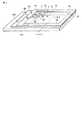
図1に、本実施形態の液晶表示装置の一例を概略的に示す。液晶表示装置は、アレイ基板110とアレイ基板110と所定の間隙をおいて対向配置された対向基板120と、アレイ基板110と対向基板120との間に挟持された液晶層70(図2に示す)と、マトリクス状に配置された表示画素PXを含む表示領域25と、を備える液晶表示パネルと、液晶表示パネルを背面側から照明するバックライトユニット130と、を備えている。Hereinafter, a liquid crystal display device according to an embodiment will be described with reference to the drawings.
FIG. 1 schematically shows an example of the liquid crystal display device of the present embodiment. The liquid crystal display device includes an
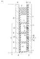
図2に、図1に示す液晶表示パネルのII−IIにおける断面の一例を示す。本実施形態の液晶表示装置は、横電界を利用して液晶層の配向状態を制御するFFSモードの液晶表示装置である。 FIG. 2 shows an example of a cross section taken along II-II of the liquid crystal display panel shown in FIG. The liquid crystal display device of the present embodiment is an FFS mode liquid crystal display device that controls the alignment state of a liquid crystal layer using a lateral electric field.
アレイ基板110は、ガラス等の透明絶縁性基板10と、透明絶縁性基板10上に配置された画素駆動配線と、スイッチング素子14と、絶縁膜L1、50と、平坦化膜20と、共通電極(第1電極)30と、センサ電極(第2電極)40と、画素電極(第3電極)60と、図示しない配向膜と、駆動回路と、を備えている。画素駆動配線は、複数の表示画素PXが配列する行に沿って延びる走査線11と、複数の表示画素PXが配列する列に沿って延びる信号線12と、を備えている。 The
駆動回路は、表示領域25の周囲を囲む額縁領域に配置された複数の走査線11を駆動する走査線駆動回路YDと、複数の信号線12を駆動する信号線駆動回路XDと、を備えている。 The drive circuit includes a scan line drive circuit YD that drives a plurality of
走査線駆動回路YDは走査線11が延びる方向における表示領域25の両脇に配置され、走査線駆動回路YDには表示領域25から延びる複数の走査線11が電気的に接続されている。信号線駆動回路XDには表示領域25から延びる複数の信号線12が電気的に接続されている。 The scanning line driving circuit YD is disposed on both sides of the
アレイ基板110の端部には図示しないフレキシブル基板が接続され、走査線駆動回路YDおよび信号線駆動回路XDには、フレキシブル基板を介して図示しない信号源から制御信号および映像信号が供給される。 A flexible substrate (not shown) is connected to the end of the
走査線11は、表示領域25においてマトリクス状に配置された表示画素PXの行に沿って延びている。信号線12は、表示領域25においてマトリクス状に配置された表示画素PXの列に沿って延びている。 The
スイッチング素子14は、走査線11と信号線12とが交差する位置近傍に配置されている。スイッチング素子14は、透明絶縁性基板10上に配置された図示しないアンダーコート層上に配置され、アモルファスシリコンあるいはポリシリコンの半導体層SCと、ゲート電極14bと、ソース電極14aと、ドレイン電極14cと、を含む薄膜トランジスタを備えている。 The
スイッチング素子14の半導体層SCの上層にはゲート絶縁膜が配置され、ゲート絶縁膜上にスイッチング素子14のゲート電極14bが配置されている。スイッチング素子14のソース電極14aとドレイン電極14cとは絶縁膜L1に設けられたコンタクトホールにおいて半導体層SCと接続されている。 A gate insulating film is disposed above the semiconductor layer SC of the
スイッチング素子14のゲート電極14bは、対応する走査線11と電気的に接続されている(あるいは一体に形成されている)。スイッチング素子14のソース電極14aは、対応する信号線12と電気的に接続されている(あるいは一体に形成されている)。スイッチング素子のドレイン電極14cは、後述するコンタクトホール21、51において対応する画素電極60と電気的に接続されている。 The
走査線駆動回路YDにより走査線11が駆動されてスイッチング素子14のゲート電極14bに電圧が印加されると、ソース電極14aとドレイン電極14cとの間が導通し、スイッチング素子14が一定期間オン状態となる。スイッチング素子14がオン状態である期間に、信号線12からスイッチング素子14を介して画素電極60へ映像信号が供給される。 When the
スイッチング素子14上には平坦化膜20が配置されている。本実施形態では、平坦化膜20は透明有機絶縁膜であって、平坦化膜20の膜厚は略3μmである。平坦化膜20は、コンタクトホール21を除いて表示領域25の全体に渡って配置されている。スイッチング素子14のドレイン電極14c上の平坦化膜20には、後述する画素電極60と電気的接続を取るためのコンタクトホール21が設けられている。平坦化膜20上には共通電極30が配置されている。 A planarizing
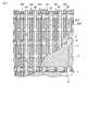
図3に、アレイ基板110の表示領域25の構成の一例を示す。なお、図3では、画素電極60とセンサ電極40とを一部省略して共通電極30の形状を示している。
カラー表示タイプの液晶表示装置である場合、複数の表示画素PXは複数種類の色画素を含んでいる。本実施形態では、複数の表示画素PXは、赤色を表示する赤色表示画素PXRと、緑色を表示する緑色表示画素PXGと、青色を表示する青色表示画素PXBと、含んでいる。赤色表示画素PXRと緑色表示画素PXGと青色表示画素PXBとの3種類の色画素により、1絵素が構成されている。表示領域25には赤色表示画素PXRと、緑色表示画素PXGと、青色表示画素PXBと、が走査線11の延びる方向に周期的に並んで配置され、信号線12が延びる方向には同種類の色画素が並んで配置されている。FIG. 3 shows an example of the configuration of the
In the case of a color display type liquid crystal display device, the plurality of display pixels PX include a plurality of types of color pixels. In the present embodiment, the plurality of display pixels PX include a red display pixel PXR that displays red, a green display pixel PXG that displays green, and a blue display pixel PXB that displays blue. One picture element is constituted by three kinds of color pixels, that is, the red display pixel PXR, the green display pixel PXG, and the blue display pixel PXB. In the
共通電極30は例えばITO(indium tin oxide)やIZO(indium zinc oxide)等の透明電極材料により形成されている。表示領域25の端部に配置された共通電極30は額縁領域へ延びて配置され、例えば外部の信号源からフレキシブル基板を介して共通電圧が印加されている。 The
共通電極30は後述のセンサ電極40との重ね合せ精度を考慮した同じパターンも盛り込み形成する。すなわち、共通電極30は複数の画素電極60と対向するように配置されている。共通電極30は、1絵素に配置された3つの画素電極60と対向するように配置されている。 The
また、コンタクトホール21には共通電極30と同じ材料で形成された接続電極31が配置されている。スイッチング素子14のドレイン電極14cと接続電極31とはコンタクトホール21において電気的に接続している。 Further, a
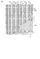
図4に、センサ電極40の一構成例を説明するための平面図を示す。なお、図4には共通電極30および接続電極31のパターン形状を破線で記載している。共通電極30上にはセンサ電極40が配置されている。 FIG. 4 is a plan view for explaining a configuration example of the
センサ電極40は、例えばアルミニウムとモリブデンとの多層電極である。センサ電極40のモリブデン層の厚さは10nm以上50nm以下であって、アルミニウム層の厚さは100nm以上400nm以下であることが望ましい。センサ電極40は2つのモリブデン層と、これらのモリブデン層の間に配置されたアルミニウム層とを備え、厚さは120nm以上500nm以下である。 The
センサ電極40は走査線11が延びる方向と略平行に延びた第1センサ40Aと信号線12が延びる方向と略平行に延びた第2センサ40Bとを含む格子状に配置され、複数の共通電極30を電気的に接続している。本実施形態では、走査線11が延びる方向の第2センサの幅および信号線12が延びる方向の第1センサの幅は略5μmである。センサ電極40は、表示領域25において共通電極30上の段差のない平坦な部分に配置されることが望ましい。 The
第2センサ40Bは、表示領域25において走査線11の延びる方向に周期的に並んで配置された赤色表示画素PXRと、緑色表示画素PXGと、青色表示画素PXBとの所定の色画素間において、信号線12の上層に配置されている。本実施形態では、第2センサ40Bは、赤色表示画素PXRと青色表示画素PXBとの間、青色表示画素PXBと緑色表示画素PXGとの間に配置されている。 The
センサ電極40は表示領域25から額縁領域へ延びて配置され、例えば外部に設けられた図示しない感知回路と電気的に接続されている。本実施形態の液晶表示装置で接触位置を検出する場合、感知回路はセンサ電極40へ所定波形の信号を供給する。ユーザの指先やペン先とセンサ電極40と距離に応じて、指先等とセンサ電極40との間に生じる容量の大きさが変化する。感知回路は、指先等とセンサ電極40との間の容量の変化によるセンサ電極40の電位の変化を、センサ電極40から出力された信号の出力波形から検出して、ユーザの指先やペン先等が接触した位置に対応するセンサ電極40の座標位置を検出する。 The
センサ電極40上には絶縁膜50が配置されている。絶縁膜50は、画素電極60と接続電極31とを電気的に接続するためのコンタクトホール51を備えている。 An insulating
絶縁膜50上には画素電極60が配置され、コンタクトホール51において接続電極31と電気的に接続している。画素電極60は、例えばITOやIZO等の透明電極材料により形成されている。画素電極60の上層には図示しない配向膜が配置されている。 A
図3に示すように、画素電極60は、互いに略平行に延びたスリット60Sを備えている。本実施形態では、複数のスリット60Sは信号線12が延びる方向と略平行に延びている。 As shown in FIG. 3, the
画素電極60と共通電極30との間、あるいは、画素電極60の端部とセンサ電極40との間に生じる電界により液晶層70の配向状態が制御される。画素電極60にスリット60Sを設けることにより、表示画素PXの中央部分においても画素電極60と共通電極30との間に電界が生じて、液晶層70の配向状態を制御することが可能となる。 The alignment state of the
対向基板120は、ガラス等の透明絶縁性基板28と、透明樹脂平坦化膜29と、複数の着色層と、図示しない配向膜とを備えている。 The
複数の着色層は、有機絶縁膜である赤(R)、緑(G)、青(B)のうちのいずれかのレジストによって着色された第1着色層24a、第2着色層24b、第3着色層24cと、黒色の第4着色層27a、第5着色層27bと、を備えている。 The plurality of colored layers are a first
赤色の第1着色層24aは赤色表示画素PXRに配置され、緑色の第2着色層24bは緑色表示画素PXGに配置され、青色の第3着色層24cは青色表示画素PXBに配置されている。第4着色層27aは表示領域25を囲むように配置され、額縁領域における光抜けを防止する遮光層である。第5着色層27bは、アレイ基板110の走査線11および信号線12と対向する位置に格子状に配置され、表示画素PX間における光抜けを防止する遮光層である。 The red first
アレイ基板110の画素電極60上および、対向基板120の透明樹脂平坦化膜29上には配向膜が配置されている。配向膜の表面はラビング処理や光学配向処理等の配向処理が成されている。 An alignment film is disposed on the
アレイ基板110と対向基板120とは、互いの配向膜が対向するように配置されシール剤26により固定される。アレイ基板110と対向基板120との間には、柱状スペーサ22が配置されている。柱状スペーサ22によりアレイ基板110と対向基板120との距離は一定に保持される。本実施形態では、柱状スペーサ22の高さは2μm以上6μm以下で任意に制御している。 The
液晶層70は、アレイ基板110、対向基板120、およびシール剤26により囲まれた領域に配置されている。 The
アレイ基板110および対向基板120の液晶層70側と反対に位置する面には図示しない偏光板が夫々配設されている。 Polarizing plates (not shown) are disposed on the surfaces of the
続いて、本実施形態の液晶表示装置の製造方法の一例について説明する。
まず、アレイ基板110を形成する方法について説明する。複数のアレイ基板110を切り出す第1透明絶縁性基板上に成膜とパターンニングとを繰り返してスイッチング素子14、走査線11、信号線12、絶縁膜L1、および、アレイ基板110上の他のスイッチング素子や各種配線を形成する。Then, an example of the manufacturing method of the liquid crystal display device of this embodiment is demonstrated.
First, a method for forming the
続いて、露光レジストを塗布、露光、現像して平坦化膜20を形成する。このとき、露光レジストは表示領域25および額縁領域の全面に塗布される。本実施形態では露光レジストは光硬化性のものを採用し、露光マスクを介してフォトレジストを露光し、現像してコンタクトホール21を有する所定パターンの平坦化膜20となるように形成する。 Subsequently, a
平坦化膜20の上にITO等の透明電極材料を成膜し、透明電極材料上にさらに露光レジストを塗布する。露光レジストを露光および現像して接続電極31および共通電極30の所定のパターンにパターンニングする。続いて、エッチングにより透明電極材料をパターンニングして、露光レジストを剥離して所定パターンの共通電極30を形成する。 A transparent electrode material such as ITO is formed on the
続いて、共通電極30の上層に、モリブデンの成膜、アルミニウムの成膜、さらにモリブデンの成膜を行い、これら多層の金属層のパターンニングを行う。共通電極30上に配置されたアルミニウムとモリブデンと積層された電極パターンを複数のグループに分けて形成し、センサ電極40を形成する。 Subsequently, molybdenum film formation, aluminum film formation, and molybdenum film formation are performed on the upper layer of the
続いて、センサ電極40上に露光レジストを塗布、露光、現像してコンタクトホール51を有する絶縁膜50を形成する。続いて、絶縁膜50上にITO等の透明電極材料を成膜し、スリット60Sを備える所定のパターンにパターンニングして画素電極60を形成する。その後、画素電極60上のアレイ基板110表面には所定方向にラビング処理や光学配向処理等の配向処理を施した配向膜80を形成する。 Subsequently, an exposure resist is applied, exposed and developed on the
図5に、センサ電極40の第2センサ40B近傍のアレイ基板110の、第2センサ40Bが延びる方向と略直交する方向における断面の一例を示す。アレイ基板110の表面には、下層に配置された導電層や絶縁層のパターン端部に沿って凹凸が生じている。特に平坦化膜20の上層に配置されている共通電極30、センサ電極40、および画素電極60のパターン端部の上層に凹凸が生じやすい。さらに、センサ電極40は複数の導電層から形成されるため他の導電層よりも比較的厚く、センサ電極40のパターン端部上には他の部分よりも大きな段差が生じやすい。そのため、センサ電極40のパターン端部上に配置された配向膜80の配向処理が適切に行われないことがある。 FIG. 5 shows an example of a cross section of the
例えば、配向膜80をラビング処理する場合には、段差部分に配置された配向膜80上をラビング布で刷り上げ又は刷り下げる際に、配向膜80にラビング布が十分に接触せずラビング処理が施されない部分Aが生じる。この配向膜80のラビング処理が施されない部分Aの近傍には、液晶分子の初期配向方向が規定されず液晶分子の配向状態を制御することができない非配向領域が発生する場合がある。例えば、センサ電極40が延びる方向と配向処理方向が略90度であると非配向領域が生じやすくなり、センサ電極40が延びる方向と配向処理方向が略40度であると非配向領域が生じにくくなる。 For example, when the
この非配向領域で光抜けが発生すると、非配向領域近傍の表示画素PXの端部が明るくなり、表示画像のコントラストが低下して表示品位が低下する原因となる。ここで、図6に示すように赤色表示画素PXRと緑色表示画素PXGとの間、緑色表示画素PXGと青色表示画素PXBとの間、および、青色表示画素PXBと赤色表示画素PXRとの間に第2センサ40Bを配置すると、非配向領域における光抜けに起因するコントラストの低下は緑色表示画素PXG、赤色表示画素PXR、青色表示画素PXBの順に顕著に視認された。 When light omission occurs in the non-alignment region, the edge of the display pixel PX in the vicinity of the non-alignment region becomes bright, which causes the contrast of the display image to decrease and the display quality to deteriorate. Here, as shown in FIG. 6, between the red display pixel PXR and the green display pixel PXG, between the green display pixel PXG and the blue display pixel PXB, and between the blue display pixel PXB and the red display pixel PXR. When the
そこで、本実施形態では、赤色表示画素PXRと青色表示画素PXBとの間、青色表示画素PXBと緑色表示画素PXGとの間にセンサ電極40の第2センサ40Bを配置し、赤色表示画素PXRと緑色表示画素PXGとの間には第2センサ40Bを配置していない。このことにより、緑色表示画素PXGおよび赤色表示画素PXRにおいて光抜けが生じてコントラストが低下することが抑制され、表示品位の良好な液晶表示装置を提供することができる。 Therefore, in the present embodiment, the
なお、本実施形態では、赤色表示画素PXRと青色表示画素PXBとの間、青色表示画素PXBと緑色表示画素PXGとの間にセンサ電極40の第2センサ40Bを配置しているが、第2センサ40Bは赤色表示画素PXRと青色表示画素PXBとの間にのみ第2センサ40Bが配置されてもよく、青色表示画素PXBと緑色表示画素PXGとの間にのみ第2センサ40Bが配置されてもよい。 In the present embodiment, the
赤色表示画素PXRと青色表示画素PXBとの間にのみ第2センサ40Bを配置すると、最もコントラストの低下が顕著である緑色表示画素PXGにおけるコントラストの低下をさらに抑制することが可能となりより表示品位の良好な液晶表示装置を提供することが可能である。 If the
青色表示画素PXBと緑色表示画素PXGとの間にのみ第2センサ40Bを配置すると、赤色表示画素PXRにおけるコントラストの低下をさらに抑制することが可能となりより表示品位の良好な液晶表示装置を提供することが可能となる。 When the
第2センサ40Bの本数は、表示領域の解像度や接触位置の検出精度に応じて設計されることが望ましい。 The number of
次に、対向基板120を形成する方法について説明する。複数の対向基板120を切り出す第2透明絶縁性基板上に、着色された露光レジストの塗布、露光、現像を繰り返して、第1着色層24a、第2着色層24b、第3着色層24c、第4着色層27a、および、第5着色層27bを形成する。さらに、複数の着色層上に透明樹脂平坦化膜29となる透明樹脂材料を塗布し、所定パターンにパターンニングして透明樹脂平坦化膜29を形成する。その後、透明樹脂平坦化膜29の表面に所定方向にラビング処理や光学配向処理等の配向処理を施した配向膜を形成する。 Next, a method for forming the
柱状スペーサ22は、第1透明絶縁性基板あるいは第2透明絶縁性基板の上層に、例えば樹脂材料を塗布し、所定パターンにパターンニングすることにより形成される。 The
続いて、表示領域25を囲むように第1透明絶縁性基板上あるいは第2透明絶縁性基板上に例えば紫外線硬化樹脂からなるシール剤26を塗布し、複数のアレイ基板110となる透明絶縁性基板と複数の対向基板120となる透明絶縁性基板とを互いの配向膜が向かい合うように対向させて位置あわせし、シール剤26に紫外線を照射して硬化させて固定する。 Subsequently, a sealing
液晶材料は、シール剤26が開口した注入口から表示領域25に注入されてもよく、第1透明絶縁性基板と第2透明絶縁性基板とを貼り合わせる前に、シール剤26に囲まれた領域に滴下されてもよい。注入口から液晶材料を注入する場合は、注入後に注入口を封止剤により封止して液晶層70が形成される。液晶材料を滴下する場合には、滴下した後に第1透明絶縁性基板と第2透明絶縁性基板とを貼り合わせて液晶層70が形成される。 The liquid crystal material may be injected into the
第1透明絶縁性基板と第2透明絶縁性基板とが貼り合わされた状態で、複数のアレイ基板110と、アレイ基板110と対向する第2透明絶縁性基板の部分とを切り出し、さらに第2透明絶縁性基板を割断して対向基板120を切り出す。 In a state where the first transparent insulating substrate and the second transparent insulating substrate are bonded together, the plurality of
続いて、アレイ基板110および対向基板120の液晶層70側と反対に位置する面に偏光板を配設して、液晶表示装置を形成する。 Subsequently, a polarizing plate is provided on the surface of the
上記のように、本実施形態によれば、赤色表示画素PXRと緑色表示画素PXGとの間に第2センサ40Bを配置しないことにより、緑色表示画素PXGおよび赤色表示画素PXRにおいてコントラストが低下することが抑制され、表示品位の良好な液晶表示装置を提供することができる。 As described above, according to the present embodiment, since the
本発明のいくつかの実施形態を説明したが、これらの実施形態は、例として提示したものであり、発明の範囲を限定することは意図していない。これら新規な実施形態は、その他の様々な形態で実施されることが可能であり、発明の要旨を逸脱しない範囲で、種々の省略、置き換え、変更を行うことができる。これら実施形態やその変形は、発明の範囲や要旨に含まれるとともに、特許請求の範囲に記載された発明とその均等の範囲に含まれる。 Although several embodiments of the present invention have been described, these embodiments are presented by way of example and are not intended to limit the scope of the invention. These novel embodiments can be implemented in various other forms, and various omissions, replacements, and changes can be made without departing from the scope of the invention. These embodiments and modifications thereof are included in the scope and gist of the invention, and are included in the invention described in the claims and the equivalents thereof.
PX…表示画素、PXR…赤色表示画素、PXG…緑色表示画素、PXB…青色表示画素、25…表示領域、30…共通電極(第1電極)、40…センサ電極(第2電極)、40A…第1センサ、40B…第2センサ、50…絶縁膜、51…コンタクトホール、60…画素電極(第3電極)、60S…スリット、70…液晶層、80…配向膜、110…アレイ基板(第1基板)、120…対向基板(第2基板)、130…バックライトユニット PX ... display pixel, PXR ... red display pixel, PXG ... green display pixel, PXB ... blue display pixel, 25 ... display region, 30 ... common electrode (first electrode), 40 ... sensor electrode (second electrode), 40A ... First sensor, 40B ... second sensor, 50 ... insulating film, 51 ... contact hole, 60 ... pixel electrode (third electrode), 60S ... slit, 70 ... liquid crystal layer, 80 ... alignment film, 110 ... array substrate (first) 1 substrate), 120 ... counter substrate (second substrate), 130 ... backlight unit
Claims (6)
Translated fromJapanese第1電極と、前記第1電極上に配置され、前記絵素の配列する行方向と略平行に延びる第1センサと前記絵素の配列する列方向と略平行に延びる第2センサとを含む第2電極と、前記第2電極の上層に配置され所定の配向方向を有する配向膜と、を備えた第1基板と、
前記第1基板と対向するように配置された第2基板と、
前記第1基板と前記第2基板との間に挟持され、前記配向膜の配向方向に初期配向方向を規定される液晶分子を含む液晶層と、を備え、
前記絵素は前記行方向において周期的に並んで配置された赤色表示画素、緑色表示画素、および、青色表示画素を含み、
前記第2センサは、前記赤色表示画素と前記青色表示画素との間に配置され、且つ、前記赤色表示画素と前記緑色表示画素との間に配置されていない液晶表示装置。A display area including a plurality of picture elements arranged in a matrix;
A first sensor disposed on the first electrode and extending substantially parallel to a row direction in which the pixels are arranged; and a second sensor extending substantially parallel to a column direction in which the pixels are arranged. A first substrate comprising: a second electrode;and an alignment film disposed on an upper layer of the second electrodeand having a predeterminedalignment direction;
A second substrate disposed to face the first substrate;
A liquid crystal layer including liquid crystal molecules sandwiched between the first substrate and the second substrate and having an initial alignment direction defined in thealignment direction of the alignment film,
The picture element includes a red display pixel, a green display pixel, and a blue display pixel that are periodically arranged in the row direction,
The second sensor is a liquid crystal display device that is disposed between the red display pixel and the blue display pixel, and is not disposed between the red display pixel and the green display pixel.
第1電極と、前記第1電極上に配置され、前記絵素の配列する行方向と略平行に延びる第1センサと前記絵素の配列する列方向と略平行に延びる第2センサとを含む第2電極と、前記第2電極の上層に配置され所定の配向方向を有する配向膜と、を備えた第1基板と、
前記第1基板と対向するように配置された第2基板と、
前記第1基板と前記第2基板との間に挟持され、前記配向膜の配向方向に初期配向方向を規定される液晶分子を含む液晶層と、を備え、
前記絵素は前記行方向において周期的に並んで配置された赤色表示画素、緑色表示画素、および、青色表示画素を含み、
前記第2センサは、前記緑色表示画素と前記青色表示画素との間に配置され、且つ、前記赤色表示画素と前記緑色表示画素との間に配置されていない液晶表示装置。A display area including a plurality of picture elements arranged in a matrix;
A first sensor disposed on the first electrode and extending substantially parallel to a row direction in which the pixels are arranged; and a second sensor extending substantially parallel to a column direction in which the pixels are arranged. A first substrate comprising: a second electrode;and an alignment film disposed on an upper layer of the second electrodeand having a predeterminedalignment direction;
A second substrate disposed to face the first substrate;
A liquid crystal layer including liquid crystal molecules sandwiched between the first substrate and the second substrate and having an initial alignment direction defined in thealignment direction of the alignment film,
The picture element includes a red display pixel, a green display pixel, and a blue display pixel that are periodically arranged in the row direction,
The second sensor is a liquid crystal display device that is disposed between the green display pixel and the blue display pixel, and is not disposed between the red display pixel and the green display pixel.
第1電極と、前記第1電極上に配置され、前記絵素の配列する行方向と略平行に延びる第1センサと前記絵素の配列する列方向と略平行に延びる第2センサとを含む第2電極と、前記第2電極の上層に配置され所定の配向方向を有する配向膜と、を備えた第1基板と、
前記第1基板と対向するように配置された第2基板と、
前記第1基板と前記第2基板との間に挟持され、前記配向膜の配向方向に初期配向方向を規定される液晶分子を含む液晶層と、を備え、
前記絵素は前記行方向において周期的に並んで配置された赤色表示画素、緑色表示画素、および、青色表示画素を含み、
前記第2センサは、行方向に隣り合う第1部分及び第2部分を有し、
前記赤色表示画素及び前記緑色表示画素は、行方向に隣り合う前記第1部分と前記第2部分との間に位置する液晶表示装置。A display area including a plurality of picture elements arranged in a matrix;
A first sensor disposed on the first electrode and extending substantially parallel to a row direction in which the pixels are arranged; and a second sensor extending substantially parallel to a column direction in which the pixels are arranged. A first substrate comprising: a second electrode;and an alignment film disposed on an upper layer of the second electrodeand having a predeterminedalignment direction;
A second substrate disposed to face the first substrate;
A liquid crystal layer including liquid crystal molecules sandwiched between the first substrate and the second substrate and having an initial alignment direction defined in thealignment direction of the alignment film,
The picture element includes a red display pixel, a green display pixel, and a blue display pixel that are periodically arranged in the row direction,
The second sensor has a first portion and a second portion that are adjacent in the row direction,
The red display pixel and the green display pixel are liquid crystal display devices positioned between the first portion and the second portion that are adjacent in the row direction.
前記青色表示画素は、前記第2部分と前記第3部分との間に位置する請求項4記載の液晶表示装置。The second sensor further includes a third portion adjacent in the row direction of the second portion,
The liquid crystal display device according to claim 4, wherein the blue display pixel is located between the second portion and the third portion.
前記第3電極は、互いに略平行に延びる複数のスリットを有している請求項1乃至請求項5のいずれか1項記載の液晶表示装置。The first substrate further includes a third electrode disposed on an upper layer of the second electrode and disposed to face the first electrode through an insulating layer,
The liquid crystal display device according to claim 1, wherein the third electrode has a plurality of slits extending substantially parallel to each other.
Priority Applications (1)
| Application Number | Priority Date | Filing Date | Title |
|---|---|---|---|
| JP2011148380AJP5840879B2 (en) | 2011-07-04 | 2011-07-04 | Liquid crystal display |
Applications Claiming Priority (1)
| Application Number | Priority Date | Filing Date | Title |
|---|---|---|---|
| JP2011148380AJP5840879B2 (en) | 2011-07-04 | 2011-07-04 | Liquid crystal display |
Related Child Applications (1)
| Application Number | Title | Priority Date | Filing Date |
|---|---|---|---|
| JP2015221319ADivisionJP6180492B2 (en) | 2015-11-11 | 2015-11-11 | Liquid crystal display |
Publications (2)
| Publication Number | Publication Date |
|---|---|
| JP2013015677A JP2013015677A (en) | 2013-01-24 |
| JP5840879B2true JP5840879B2 (en) | 2016-01-06 |
Family
ID=47688407
Family Applications (1)
| Application Number | Title | Priority Date | Filing Date |
|---|---|---|---|
| JP2011148380AActiveJP5840879B2 (en) | 2011-07-04 | 2011-07-04 | Liquid crystal display |
Country Status (1)
| Country | Link |
|---|---|
| JP (1) | JP5840879B2 (en) |
Families Citing this family (2)
| Publication number | Priority date | Publication date | Assignee | Title |
|---|---|---|---|---|
| JP2016038539A (en)* | 2014-08-11 | 2016-03-22 | 株式会社ジャパンディスプレイ | Liquid crystal display |
| KR101719397B1 (en)* | 2014-08-14 | 2017-03-24 | 엘지디스플레이 주식회사 | Touch sensor integrated type liquid crystal display device |
Family Cites Families (1)
| Publication number | Priority date | Publication date | Assignee | Title |
|---|---|---|---|---|
| US8217913B2 (en)* | 2009-02-02 | 2012-07-10 | Apple Inc. | Integrated touch screen |
- 2011
- 2011-07-04JPJP2011148380Apatent/JP5840879B2/enactiveActive
Also Published As
| Publication number | Publication date |
|---|---|
| JP2013015677A (en) | 2013-01-24 |
Similar Documents
| Publication | Publication Date | Title |
|---|---|---|
| JP5526085B2 (en) | Liquid crystal display | |
| US12345984B2 (en) | Liquid crystal display apparatus | |
| US20200278584A1 (en) | Liquid crystal display device | |
| JP2011013618A (en) | Liquid crystal display device | |
| JP5771550B2 (en) | Liquid crystal display | |
| JP2020140089A (en) | In-cell touch panel | |
| US8797466B2 (en) | Liquid crystal display | |
| JP5544330B2 (en) | Liquid crystal display | |
| JP5840879B2 (en) | Liquid crystal display | |
| JP2016139073A (en) | Liquid crystal display | |
| JP6780062B2 (en) | Liquid crystal display device | |
| JP6180492B2 (en) | Liquid crystal display | |
| JP6539309B2 (en) | Liquid crystal display | |
| JP2013205625A (en) | Liquid crystal display device | |
| JP5919133B2 (en) | Liquid crystal display | |
| JP6055626B2 (en) | Liquid crystal display | |
| JP5450741B2 (en) | Liquid crystal display | |
| JP2012083959A (en) | Touch panel and image display device | |
| JP2014202948A (en) | Liquid crystal display device and method of manufacturing liquid crystal display device | |
| JP2010204474A (en) | Liquid crystal display device |
Legal Events
| Date | Code | Title | Description |
|---|---|---|---|
| A711 | Notification of change in applicant | Free format text:JAPANESE INTERMEDIATE CODE: A712 Effective date:20130711 | |
| A621 | Written request for application examination | Free format text:JAPANESE INTERMEDIATE CODE: A621 Effective date:20140630 | |
| A131 | Notification of reasons for refusal | Free format text:JAPANESE INTERMEDIATE CODE: A131 Effective date:20150127 | |
| A977 | Report on retrieval | Free format text:JAPANESE INTERMEDIATE CODE: A971007 Effective date:20150128 | |
| A521 | Request for written amendment filed | Free format text:JAPANESE INTERMEDIATE CODE: A523 Effective date:20150325 | |
| A131 | Notification of reasons for refusal | Free format text:JAPANESE INTERMEDIATE CODE: A131 Effective date:20150414 | |
| A521 | Request for written amendment filed | Free format text:JAPANESE INTERMEDIATE CODE: A523 Effective date:20150520 | |
| A131 | Notification of reasons for refusal | Free format text:JAPANESE INTERMEDIATE CODE: A131 Effective date:20150804 | |
| A521 | Request for written amendment filed | Free format text:JAPANESE INTERMEDIATE CODE: A523 Effective date:20150915 | |
| TRDD | Decision of grant or rejection written | ||
| A01 | Written decision to grant a patent or to grant a registration (utility model) | Free format text:JAPANESE INTERMEDIATE CODE: A01 Effective date:20151013 | |
| A61 | First payment of annual fees (during grant procedure) | Free format text:JAPANESE INTERMEDIATE CODE: A61 Effective date:20151112 | |
| R150 | Certificate of patent or registration of utility model | Ref document number:5840879 Country of ref document:JP Free format text:JAPANESE INTERMEDIATE CODE: R150 | |
| R250 | Receipt of annual fees | Free format text:JAPANESE INTERMEDIATE CODE: R250 | |
| R250 | Receipt of annual fees | Free format text:JAPANESE INTERMEDIATE CODE: R250 | |
| R250 | Receipt of annual fees | Free format text:JAPANESE INTERMEDIATE CODE: R250 | |
| R250 | Receipt of annual fees | Free format text:JAPANESE INTERMEDIATE CODE: R250 | |
| R250 | Receipt of annual fees | Free format text:JAPANESE INTERMEDIATE CODE: R250 | |
| R250 | Receipt of annual fees | Free format text:JAPANESE INTERMEDIATE CODE: R250 | |
| R250 | Receipt of annual fees | Free format text:JAPANESE INTERMEDIATE CODE: R250 | |
| S111 | Request for change of ownership or part of ownership | Free format text:JAPANESE INTERMEDIATE CODE: R313113 | |
| R350 | Written notification of registration of transfer | Free format text:JAPANESE INTERMEDIATE CODE: R350 |