JP5836067B2 - Luminous flux control member, light emitting device, surface light source device, and display device - Google Patents
Luminous flux control member, light emitting device, surface light source device, and display deviceDownload PDFInfo
- Publication number
- JP5836067B2 JP5836067B2JP2011238570AJP2011238570AJP5836067B2JP 5836067 B2JP5836067 B2JP 5836067B2JP 2011238570 AJP2011238570 AJP 2011238570AJP 2011238570 AJP2011238570 AJP 2011238570AJP 5836067 B2JP5836067 B2JP 5836067B2
- Authority
- JP
- Japan
- Prior art keywords
- light
- flux controlling
- controlling member
- gate
- back surface
- Prior art date
- Legal status (The legal status is an assumption and is not a legal conclusion. Google has not performed a legal analysis and makes no representation as to the accuracy of the status listed.)
- Active
Links
- 230000004907fluxEffects0.000titleclaimsdescription141
- 239000011347resinSubstances0.000claimsdescription23
- 229920005989resinPolymers0.000claimsdescription23
- 238000002347injectionMethods0.000claimsdescription21
- 239000007924injectionSubstances0.000claimsdescription21
- 238000001746injection mouldingMethods0.000claimsdescription16
- 230000003287optical effectEffects0.000claimsdescription9
- 238000000034methodMethods0.000description26
- 238000005520cutting processMethods0.000description12
- 239000000758substrateSubstances0.000description11
- 230000002093peripheral effectEffects0.000description9
- 238000010586diagramMethods0.000description8
- 238000009826distributionMethods0.000description7
- 230000000694effectsEffects0.000description7
- 239000004973liquid crystal related substanceSubstances0.000description7
- 238000009792diffusion processMethods0.000description6
- 229920003229poly(methyl methacrylate)Polymers0.000description4
- 239000004926polymethyl methacrylateSubstances0.000description4
- 238000004519manufacturing processMethods0.000description3
- 239000000463materialSubstances0.000description3
- PPBRXRYQALVLMV-UHFFFAOYSA-NStyreneChemical compoundC=CC1=CC=CC=C1PPBRXRYQALVLMV-UHFFFAOYSA-N0.000description2
- 239000003822epoxy resinSubstances0.000description2
- 239000004417polycarbonateSubstances0.000description2
- 229920000515polycarbonatePolymers0.000description2
- 229920000647polyepoxidePolymers0.000description2
- VVQNEPGJFQJSBK-UHFFFAOYSA-NMethyl methacrylateChemical compoundCOC(=O)C(C)=CVVQNEPGJFQJSBK-UHFFFAOYSA-N0.000description1
- 239000004793PolystyreneSubstances0.000description1
- 239000011324beadSubstances0.000description1
- 210000000078clawAnatomy0.000description1
- 229920006026co-polymeric resinPolymers0.000description1
- 238000005286illuminationMethods0.000description1
- 239000011159matrix materialSubstances0.000description1
Images


Classifications
- G—PHYSICS
- G02—OPTICS
- G02B—OPTICAL ELEMENTS, SYSTEMS OR APPARATUS
- G02B3/00—Simple or compound lenses
- G02B3/0006—Arrays
- G02B3/0037—Arrays characterized by the distribution or form of lenses
- G02B3/0056—Arrays characterized by the distribution or form of lenses arranged along two different directions in a plane, e.g. honeycomb arrangement of lenses
- G—PHYSICS
- G02—OPTICS
- G02B—OPTICAL ELEMENTS, SYSTEMS OR APPARATUS
- G02B19/00—Condensers, e.g. light collectors or similar non-imaging optics
- G02B19/0004—Condensers, e.g. light collectors or similar non-imaging optics characterised by the optical means employed
- G02B19/0009—Condensers, e.g. light collectors or similar non-imaging optics characterised by the optical means employed having refractive surfaces only
- G02B19/0014—Condensers, e.g. light collectors or similar non-imaging optics characterised by the optical means employed having refractive surfaces only at least one surface having optical power
- G—PHYSICS
- G02—OPTICS
- G02B—OPTICAL ELEMENTS, SYSTEMS OR APPARATUS
- G02B19/00—Condensers, e.g. light collectors or similar non-imaging optics
- G02B19/0033—Condensers, e.g. light collectors or similar non-imaging optics characterised by the use
- G02B19/0047—Condensers, e.g. light collectors or similar non-imaging optics characterised by the use for use with a light source
- G02B19/0061—Condensers, e.g. light collectors or similar non-imaging optics characterised by the use for use with a light source the light source comprising a LED
- G—PHYSICS
- G02—OPTICS
- G02F—OPTICAL DEVICES OR ARRANGEMENTS FOR THE CONTROL OF LIGHT BY MODIFICATION OF THE OPTICAL PROPERTIES OF THE MEDIA OF THE ELEMENTS INVOLVED THEREIN; NON-LINEAR OPTICS; FREQUENCY-CHANGING OF LIGHT; OPTICAL LOGIC ELEMENTS; OPTICAL ANALOGUE/DIGITAL CONVERTERS
- G02F1/00—Devices or arrangements for the control of the intensity, colour, phase, polarisation or direction of light arriving from an independent light source, e.g. switching, gating or modulating; Non-linear optics
- G02F1/01—Devices or arrangements for the control of the intensity, colour, phase, polarisation or direction of light arriving from an independent light source, e.g. switching, gating or modulating; Non-linear optics for the control of the intensity, phase, polarisation or colour
- G02F1/13—Devices or arrangements for the control of the intensity, colour, phase, polarisation or direction of light arriving from an independent light source, e.g. switching, gating or modulating; Non-linear optics for the control of the intensity, phase, polarisation or colour based on liquid crystals, e.g. single liquid crystal display cells
- G02F1/133—Constructional arrangements; Operation of liquid crystal cells; Circuit arrangements
- G02F1/1333—Constructional arrangements; Manufacturing methods
- G02F1/1335—Structural association of cells with optical devices, e.g. polarisers or reflectors
- G02F1/1336—Illuminating devices
- G02F1/133602—Direct backlight
- G02F1/133603—Direct backlight with LEDs
Landscapes
- Physics & Mathematics (AREA)
- General Physics & Mathematics (AREA)
- Optics & Photonics (AREA)
- Nonlinear Science (AREA)
- Mathematical Physics (AREA)
- Chemical & Material Sciences (AREA)
- Crystallography & Structural Chemistry (AREA)
- Planar Illumination Modules (AREA)
Description
Translated fromJapanese本発明は、発光素子から出射された光の進行方向を制御する光束制御部材であって、射出成形により形成された光束制御部材に関する。また、本発明は、前記光束制御部材を有する発光装置、前記発光装置を有する面光源装置、および前記面光源装置を有する表示装置に関する。 The present invention relates to a light flux controlling member that controls the traveling direction of light emitted from a light emitting element, and relates to a light flux controlling member formed by injection molding. The present invention also relates to a light emitting device having the light flux controlling member, a surface light source device having the light emitting device, and a display device having the surface light source device.
液晶表示装置などの透過型画像表示装置では、バックライトとして直下型の面光源装置を使用することがある。近年、光源として複数の発光ダイオード(LED)を有する、直下型の面光源装置が使用されるようになってきている。 In a transmissive image display device such as a liquid crystal display device, a direct-type surface light source device may be used as a backlight. In recent years, direct type surface light source devices having a plurality of light emitting diodes (LEDs) as light sources have been used.
たとえば、直下型の面光源装置は、基板、複数のLED、複数の光束制御部材(拡散レンズ)および光拡散部材(拡散板)を有する。複数のLEDは、基板上にマトリックス状に配置されている。各LEDの上には、各LEDから出射された光を基板の面方向に拡げる光束制御部材が配置されている。光束制御部材から出射された光は、光拡散部材により拡散され、被照射部材(例えば液晶パネル)を面状に照らす。 For example, a direct type surface light source device includes a substrate, a plurality of LEDs, a plurality of light flux control members (diffuse lenses), and a light diffusion member (diffuser plate). The plurality of LEDs are arranged in a matrix on the substrate. On each LED, a light flux controlling member that spreads light emitted from each LED in the surface direction of the substrate is disposed. The light emitted from the light flux controlling member is diffused by the light diffusing member and illuminates the irradiated member (for example, a liquid crystal panel) in a planar shape.
特許文献1には、直下型の面光源装置に使用される光束制御部材(拡散レンズ)を、透明樹脂を用いて射出成形により製造することが開示されている。また、射出成形により出射面の外周部に形成されたゲート残り(サイドゲート)を、光束制御部材の位置決めに利用することが開示されている。 Patent Document 1 discloses that a light flux controlling member (diffuse lens) used in a direct type surface light source device is manufactured by injection molding using a transparent resin. In addition, it is disclosed that the remaining gate (side gate) formed on the outer peripheral portion of the emission surface by injection molding is used for positioning the light flux controlling member.
特許文献1に記載されているように、出射面の外周部にゲート跡(ゲート残りまたはゲート切断箇所)が存在すると、このゲート跡において光が散乱してしまうため、所望の配光特性を実現することができない。この問題を改善する手段としては、射出成形金型のゲート(樹脂注入口)の厚みを薄くすることが考えられるが、ゲートの厚みを過度に薄くすることは成形性の観点から好ましくない。 As described in Patent Document 1, if there is a gate trace (gate residue or gate cut location) on the outer peripheral portion of the emission surface, light is scattered at the gate trace, so that a desired light distribution characteristic is realized. Can not do it. As a means for improving this problem, it is conceivable to reduce the thickness of the gate (resin injection port) of the injection mold, but it is not preferable from the viewpoint of moldability to make the gate too thin.
本発明は、かかる点に鑑みてなされたものであり、射出成形により形成される光束制御部材であって、射出成形金型のゲートの厚みを確保しつつ、ゲート跡による配光特性への影響が小さい光束制御部材を提供することを目的とする。また、本発明は、この光束制御部材を有する発光装置、この発光装置を有する面光源装置、およびこの面光源装置を有する表示装置を提供することも目的とする。 The present invention has been made in view of the above points, and is a light flux control member formed by injection molding, and has an effect on light distribution characteristics due to the gate trace while ensuring the thickness of the gate of the injection mold. It aims at providing the light beam control member with small. Another object of the present invention is to provide a light emitting device having the light flux controlling member, a surface light source device having the light emitting device, and a display device having the surface light source device.
本発明の光束制御部材は、発光素子から出射された光の進行方向を制御する、射出成形により形成された光束制御部材であって、発光素子から出射された光の進行方向を制御する光制御出射面と、前記光制御出射面の反対側に位置する裏面と、前記裏面の外縁に接するように前記裏面の一部に形成されたゲート跡とを有する構成を採る。 The light flux controlling member of the present invention is a light flux controlling member formed by injection molding for controlling the traveling direction of the light emitted from the light emitting element, and controls the traveling direction of the light emitted from the light emitting element. A structure having an emission surface, a back surface located on the opposite side of the light control emission surface, and a gate mark formed on a part of the back surface so as to contact an outer edge of the back surface is adopted.
本発明の発光装置は、発光素子と、本発明の光束制御部材とを有し、前記光束制御部材は、前記光制御出射面の中心軸が前記発光素子の光軸と一致するように配置されている構成を採る。 The light emitting device of the present invention includes a light emitting element and the light flux controlling member of the present invention, and the light flux controlling member is disposed so that a central axis of the light control emitting surface coincides with an optical axis of the light emitting element. Take the configuration that is.
本発明の面光源装置は、本発明の発光装置と、前記発光装置からの光を拡散させつつ透過させる光拡散部材とを有する構成を採る。 The surface light source device of the present invention employs a configuration having the light emitting device of the present invention and a light diffusing member that diffuses and transmits light from the light emitting device.
本発明の表示装置は、本発明の面光源装置と、前記面光源装置からの光を照射される被照射部材とを有する構成を採る。 The display device of the present invention employs a configuration having the surface light source device of the present invention and an irradiated member that is irradiated with light from the surface light source device.
本発明の光束制御部材は、射出成形金型のゲートの厚みを確保しつつ、ゲート跡による配光特性への影響が小さくなるように製造されうる。このため、本発明の光束制御部材は、容易に製造することが可能であり、かつ優れた配光特性を示す。 The light flux controlling member of the present invention can be manufactured so that the influence of the gate trace on the light distribution characteristics is reduced while securing the thickness of the gate of the injection mold. For this reason, the light flux controlling member of the present invention can be easily manufactured, and exhibits excellent light distribution characteristics.
また、本発明の発光装置は、本発明の光束制御部材の光制御出射面を有効に利用して、発光素子から出射された光を大きく拡げることができる。したがって、本発明の発光装置を含む本発明の面光源装置は、その厚みを薄くしても、面状の被照射部材を均一に照らすことができる。このため、本発明の面光源装置を含む本発明の表示装置の厚みを薄くすることもできる。 Further, the light emitting device of the present invention can greatly expand the light emitted from the light emitting element by effectively utilizing the light control emitting surface of the light flux controlling member of the present invention. Therefore, the surface light source device of the present invention including the light emitting device of the present invention can uniformly illuminate the planar irradiated member even if the thickness thereof is reduced. For this reason, the thickness of the display device of the present invention including the surface light source device of the present invention can be reduced.
以下、本発明の実施の形態について、図面を参照して詳細に説明する。以下の説明では、本発明の面光源装置の代表例として、液晶表示装置のバックライトなどに適する面光源装置について説明する。これらの面光源装置は、液晶パネルなどの被照射部材と組み合わせることで、表示装置として使用されうる。 Hereinafter, embodiments of the present invention will be described in detail with reference to the drawings. In the following description, a surface light source device suitable for a backlight of a liquid crystal display device will be described as a representative example of the surface light source device of the present invention. These surface light source devices can be used as a display device by combining with an irradiated member such as a liquid crystal panel.
(実施の形態1)
[面光源装置および発光装置の構成]
図1は、本発明の実施の形態1の面光源装置の構成を示す平面図である。図2は、図1に示されるA−A線の断面図である。(Embodiment 1)
[Configuration of surface light source device and light emitting device]
FIG. 1 is a plan view showing the configuration of the surface light source device according to Embodiment 1 of the present invention. 2 is a cross-sectional view taken along line AA shown in FIG.
図1および図2に示されるように、実施の形態1の面光源装置100は、基板110、複数の発光装置120、および光拡散部材150を有する。 As shown in FIGS. 1 and 2, the surface
複数の発光装置120は、所定の配列および間隔で基板110の上に配置されている。複数の発光装置120は、それぞれ発光素子130および光束制御部材140を有している。 The plurality of
発光素子130は、面光源装置100(および発光装置120)の光源であり、基板110の上に固定されている。発光素子130は、例えば白色発光ダイオードなどの発光ダイオード(LED)である。 The
光束制御部材140は、発光素子130から出射された光の進行方向を制御する拡散レンズである。光束制御部材140は、光制御出射面141(後述)の中心軸CAが発光素子130の光軸LAに一致するように、発光素子130の上に配置されている。また、発光素子130の発光面131と光束制御部材140の裏面142との間には、隙間が形成されている(図2参照)。隙間を形成する理由としては、発光素子130から発せられる熱を放熱するためという積極的理由と、光束制御部材140を配置する際の位置誤差の影響を小さくするためという消極的理由がある。 The light
光束制御部材140は、射出成形により形成されている。光束制御部材140の材料は、射出成形により成形することが可能であり、かつ所望の波長の光を通過させ得る材料であれば特に限定されない。たとえば、光束制御部材140の材料は、ポリメタクリル酸メチル(PMMA)やポリカーボネート(PC)、エポキシ樹脂(EP)などの光透過性樹脂である。 The light
本発明の面光源装置100は、光束制御部材140の構成に主たる特徴を有する。そこで、光束制御部材140については、別途詳細に説明する。 The surface
光拡散部材150は、光拡散性を有する板状の部材であり、光束制御部材140からの出射光を拡散させつつ透過させる。通常、光拡散部材150は、液晶パネルなどの被照射部材とほぼ同じ大きさである。たとえば、光拡散部材150は、ポリメタクリル酸メチル(PMMA)、ポリカーボネート(PC)、ポリスチレン(PS)、スチレン・メチルメタクリレート共重合樹脂(MS)などの光透過性樹脂により形成される。光拡散性を付与するため、光拡散部材150の表面に微細な凹凸が形成されているか、または光拡散部材150の内部にビーズなどの光拡散子が分散している。 The
本発明の面光源装置100では、各発光素子130から出射された光は、光束制御部材140により基板110の面方向に拡げられ、さらに光拡散部材150により拡散される。その結果、本発明の面光源装置100は、面状の被照射部材(例えば液晶パネル)を均一に照らすことができる。 In the surface
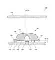
[光束制御部材の構成]
図3は、実施の形態1の光束制御部材140の構成を示す図である。図3Aは、光束制御部材140の平面図であり、図3Bは、光束制御部材140の正面図であり、図3Cは、光束制御部材140の側面図であり、図3Dは、光束制御部材140の底面図である。また、図3Eは、図3Aに示されるD−D線の断面図である。[Configuration of luminous flux control member]
FIG. 3 is a diagram illustrating a configuration of the light
図3A〜Eに示されるように、光束制御部材140は、光制御出射面141、裏面142、凹部143、鍔部145および複数の脚部146を有する。 As illustrated in FIGS. 3A to 3E, the light
光制御出射面141は、発光素子130から出射され、光束制御部材140の内部に入射した光の進行方向を制御する。光制御出射面141は、中心軸CAを軸とする回転対称面であり(図2参照)、鍔部145よりも上側(光拡散部材150側)に向けて突出している。 The light
光制御出射面141は、光制御出射面141の中心軸CAを中心とする所定範囲に位置する第1の出射面141aと、第1の出射面141aの周囲に連続して形成される第2の出射面141bと、第2の出射面141bと鍔部145とを接続する第3の出射面141cとを有する(図3E参照)。第1の出射面141aは、下側(発光素子130側)に凸の滑らかな曲面である。第1の出射面141aの形状は、球面の一部を切り取ったような凹形状である。第2の出射面141bは、第1の出射面141aの周囲に位置する、上側(光拡散部材150側)に凸の滑らかな曲面である。第2の出射面141bの形状は、円環面の一部を切り取ったような凸形状である。第3の出射面141cは、第2の出射面141bの周囲に位置する曲面である。図3Eに示される断面において、第3の出射面141cの断面は、直線状であってもよいし、曲線状であってもよい。 The light
凹部143は、光束制御部材140の下側(発光素子130側)の中央部に形成されている。凹部143の内面144は、発光素子130から出射された光のうち、発光素子130の光軸LAに対して所定の角度の範囲内で出射された光(主光線)を、光束制御部材140の内部に入射させる。裏面142は、光制御出射面141の反対側に位置し、凹部143の開口縁部から径方向に延在する平面である。裏面142は、発光素子130から出射された光のうち、主光線以外の光(副光線)を、光束制御部材140の内部に入射させる。 The
鍔部145は、光制御出射面141の外周部と裏面142の外周部との間に位置し、径方向外側に突出している。鍔部145の形状は、略円環状である。鍔部145は、必ずしも必要ではないが、鍔部145を設けることで、光束制御部材140の取り扱いおよび位置合わせが容易になる。鍔部145の厚みは、特に限定されず、光制御出射面141の必要面積や鍔部145の成形性などを考慮して決定される。たとえば、鍔部145の厚みは、0.8mm程度である。 The
複数の脚部146は、裏面142の外周部に、裏面142から下側(発光素子130側)に向かって突出している円柱状の部材である。複数の脚部146は、発光素子130に対して適切な位置に光束制御部材140を支持する。脚部146の高さは、特に限定されないが、例えば1mm程度である。 The plurality of
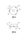
ここで、本発明の主たる特徴について説明する。本発明の光束制御部材は、射出成形により形成される。したがって、本発明の光束制御部材には、ゲート方式に応じたゲート跡(樹脂注入跡)が形成される。射出成形におけるゲート方式には、ダイレクトゲート方式や、サイドゲート方式、ピンゲート方式など様々なものがあるが、本発明の光束制御部材は、オーバーラップゲート方式、またはオーバーラップゲート方式とサイドゲート方式との組み合わせで形成されることを一つの特徴とする。「オーバーラップゲート方式」とは、ゲート部が光束制御部材の裏面に接続される(重なる)方式をいう。また、「サイドゲート方式」とは、ゲート部が光束制御部材の側面に接続される方式をいう。したがって、本発明の光束制御部材では、少なくとも裏面にゲート跡(ゲート残りまたはゲート切断箇所)が存在する。オーバーラップゲート方式を採用することにより得られる効果については、後述する。 Here, the main features of the present invention will be described. The light flux controlling member of the present invention is formed by injection molding. Therefore, a gate mark (resin injection mark) corresponding to the gate system is formed on the light flux controlling member of the present invention. There are various gate methods in injection molding, such as a direct gate method, a side gate method, and a pin gate method, but the light flux controlling member of the present invention is an overlap gate method, or an overlap gate method and a side gate method. One feature is that it is formed by a combination of the above. The “overlap gate method” is a method in which the gate portion is connected (overlapped) to the back surface of the light flux controlling member. Further, the “side gate method” refers to a method in which the gate portion is connected to the side surface of the light flux controlling member. Therefore, in the light flux controlling member of the present invention, there is a gate mark (a gate residue or a gate cut portion) on at least the back surface. The effect obtained by adopting the overlap gate method will be described later.
図4Aは、ゲートカット前の実施の形態1の光束制御部材140の底面図であり、図4Bは、ゲートカット前の光束制御部材140の正面図である。また、図4Cは、ゲートカット後の光束制御部材140の底面図であり、図4Dは、ゲートカット後の光束制御部材140の正面図である。なお、図4Cは、図3Cと同一図面であり、図4Dは、図3Bと同一図面である。 FIG. 4A is a bottom view of light
また、図5Aは、実施の形態1の光束制御部材140における樹脂注入領域149の位置を示す底面図であり、図5Bは、実施の形態1の光束制御部材140における樹脂注入領域149の位置を示す側面図である。樹脂注入領域149とは、光束制御部材140の本体部分に対するゲート部148(ゲート残り147)の接続領域を意味する。樹脂注入領域149は、射出成形金型のキャビティ部への樹脂注入口に対応する。なお、図5Aおよび図5Bでは、ゲート残り147を省略している。 5A is a bottom view showing the position of the
図4Aおよび図4Bに示されるように、実施の形態1の光束制御部材140は、オーバーラップゲート方式とサイドゲート方式とを組み合わせて形成される。このため、ゲート部148は、図5Aおよび図5Bに示されるように、光束制御部材140の裏面142の一部および鍔部145の側面の一部に接続される。このゲート部148を切断することで、ゲート跡であるゲート残り147が形成される。 As shown in FIGS. 4A and 4B, the light
図4Cおよび図5Aに示されるように、ゲート残り147は、裏面142の外周部の一部(裏面142の外縁に接する領域)に接続されている。また、図4Dおよび図5Bに示されるように、ゲート残り147は、鍔部145の側面の一部(裏面142に隣接する領域)にも接続されている。 As shown in FIGS. 4C and 5A, the remaining
オーバーラップゲート方式で光束制御部材140を形成した場合、樹脂注入領域149は、裏面142の外縁に接する。これに対し、ピンゲート方式で形成した場合は、樹脂注入領域149は、裏面142の外縁に接することはない。また、ピンゲート方式で形成した場合は、金型を開くのと同時に製品(光束制御部材140)とゲート部148とが切り離されるが、オーバーラップゲート方式で形成した場合は、ゲート部148を残さずにゲート部を切り離すことは困難であるため、ゲート残り147が形成されることが多い。 When the light
また、実施の形態1の光束制御部材140において、裏面142に接続しているゲート残り147の形状は、略三角柱状である。すなわち、ゲート残り147を構成する面のうち、裏面142の樹脂注入領域149に対向する面は、裏面142に対して傾斜している。これは、射出成形時のゲート内の樹脂の流れ方向が、裏面の樹脂注入口に対して斜めであることを意味する。このようにすることで、樹脂の流動圧力を効率よく利用して、射出成形時の樹脂流動性を向上させることができる。これに対し、ピンゲート方式では、射出成形時の樹脂注入口手前のゲート内の樹脂の流れ方向が、樹脂注入口が形成される面に対して垂直である。 In the light
このように、ゲート跡の位置や形状などにより、オーバーラップゲート方式とピンゲート方式のどちらを採用しているかを確認することができる。 Thus, it can be confirmed whether the overlap gate method or the pin gate method is adopted according to the position and shape of the gate mark.
ゲート残り147(ゲート部148の一端)の幅および高さは、成形性を考慮して決定される。たとえば、ゲート残り147の幅(図4CにおけるW)は、2mm程度であり、ゲート残りの高さ(図4DにおけるH)は、1.2mm程度である。 The width and height of the remaining gate 147 (one end of the gate portion 148) are determined in consideration of formability. For example, the width of the remaining gate 147 (W in FIG. 4C) is about 2 mm, and the height of the remaining gate (H in FIG. 4D) is about 1.2 mm.
図2に示されるように、裏面142から下側(発光素子130側)に向かってのゲート残り147の高さh1は、裏面142から下側に向かっての脚部146の高さh2よりも低い。ゲート残り147の高さh1が脚部146の高さh2以上の場合、光束制御部材140を基板110上に配置する際に、ゲート残り147が基板110に干渉してしまう。より確実に干渉を防ぐ観点からは、ゲート残り147の高さh1は、脚部146の高さh2よりも0.2mm以上低いことが好ましい。 As shown in FIG. 2, the height h1 of the remaining
図6Aは、ゲートカット前の従来の光束制御部材(第1の例)の正面図であり、図6Bは、ゲートカット後の従来の光束制御部材(第1の例)の正面図である。図6Cは、ゲートカット前の従来の光束制御部材(第2の例)の正面図であり、図6Dは、ゲートカット後の従来の光束制御部材(第2の例)の正面図である。図6Eは、ゲートカット前の従来の光束制御部材(第3の例)の正面図であり、図6Fは、ゲートカット後の従来の光束制御部材(第3の例)の正面図である。図6Gは、ゲートカット前の実施の形態1の光束制御部材140の正面図であり、図6Hは、ゲートカット後の実施の形態1の光束制御部材140の正面図である。なお、図6Gは、図4Bと同一図面であり、図6Hは、図4Dと同一図面である。 6A is a front view of a conventional light flux controlling member (first example) before gate cutting, and FIG. 6B is a front view of a conventional light flux controlling member (first example) after gate cutting. FIG. 6C is a front view of a conventional light flux controlling member (second example) before gate cutting, and FIG. 6D is a front view of a conventional light flux controlling member (second example) after gate cutting. FIG. 6E is a front view of a conventional light flux control member (third example) before gate cut, and FIG. 6F is a front view of a conventional light flux control member (third example) after gate cut. 6G is a front view of light
図6Aおよび図6Bに示されるように、従来の光束制御部材は、鍔部145の厚みが大きかった。このため、従来の光束制御部材は、鍔部145の側面にゲート部148が接続されるように形成されていた。ところが、近年、光束制御部材内に取り込んだ発光素子からの光について、より多くの光を制御して出射させるために、光制御出射面141の面積を大きくすることが要求されるようになってきた。このため、図6Cおよび図6D、ならびに図6Eおよび図6Fに示されるように、鍔部145の厚みを小さくして、光制御出射面141の面積を大きくするようになってきた。 As shown in FIGS. 6A and 6B, in the conventional light flux controlling member, the thickness of the
図6Cおよび図6Dに示されるように、鍔部145の厚みが一定の厚み以上であれば、鍔部145の側面にのみゲート部148を接続した状態で、光束制御部材を形成することができる。しかしながら、図6Eおよび図6Fに示されるように、鍔部145の厚みが一定の厚み未満となってしまうと、ゲート部148の厚みが鍔部145の厚みを上回ってしまうことになる。この問題を改善する手段としては、ゲート部148の厚みを薄くすることが考えられるが、成形性の観点からは、ゲート部148の厚みはある程度必要となる。このため、鍔部145の厚みが小さい従来の光束制御部材は、ゲート部148が光制御出射面141の外周部にも接続するように形成されていた。 As shown in FIGS. 6C and 6D, if the thickness of the
これに対し、図6Gおよび図6Hに示されるように、実施の形態1の光束制御部材140では、ゲート部148を光制御出射面141に接続させる代わりに、裏面142に接続させることとした。すなわち、ゲート部148の厚みを維持しつつ、ゲート部148の接続位置を下側(発光素子130側)に移動させた。 On the other hand, as shown in FIGS. 6G and 6H, in light
[効果]
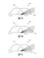
図7Aは、ゲート跡が生じない製造方法(例えば、切削加工)により形成された光束制御部材140’における光路の一例を示す断面図である。この図に示されるように、ゲート跡を有しない光束制御部材140’では、光制御出射面141の全面を使用して、発光素子130から出射された光の方向を制御することができる。しかしながら、製造コストの観点からは、切削加工などよりも射出成形により光束制御部材を製造することが好ましい。[effect]
FIG. 7A is a cross-sectional view illustrating an example of an optical path in a light
図7Bは、射出成形により形成された従来の光束制御部材140”(図6F参照)における光路の一例を示す断面図である。この図に示されるように、従来の光束制御部材140”では、ゲート跡(ゲート残り147)が光制御出射面141の一部にも形成されてしまっている。このような場合、図7Bに示されるように、発光素子130から出射された光の一部がゲート跡(ゲート残り147)において意図しない方向に反射してしまい、所望の配光を実現することができない。すなわち、図7Aの光束制御部材140’に比べて、光束制御部材140”によって制御可能な光量は少なくなる。 FIG. 7B is a cross-sectional view showing an example of an optical path in a conventional light
一方、図7Cは、射出成形により形成された実施の形態1の光束制御部材140における光路の一例を示す断面図である。この図に示されるように、実施の形態1の光束制御部材140では、ゲート跡(ゲート残り147)が光制御出射面141に形成されていない。したがって、切削加工により形成された光束制御部材140’(図7A参照)と同様に、実施の形態1の光束制御部材140では、光制御出射面141の全面を使用して、発光素子130から出射された光の方向を制御することができる。 On the other hand, FIG. 7C is a cross-sectional view showing an example of an optical path in light
このように、本実施の形態の光束制御部材140では、射出成形金型のゲートの厚みを確保しつつ、ゲート跡による配光特性への影響が小さい。このため、本実施の形態の光束制御部材140は、容易に製造することが可能であり、かつ優れた配光特性を有する。 As described above, in the light
また、本実施の形態の光束制御部材140は、光制御出射面141の外周部も有効に利用して、発光素子130から出射された光を効率的に拡げることができる。したがって、本実施の形態の光束制御部材140を含む面光源装置100は、その厚みを薄くしても、面状の被照射部材を均一に照らすことができる。 Further, the light
(実施の形態2)
[面光源装置および発光装置の構成]
本発明の実施の形態2の面光源装置および発光装置は、実施の形態1の光束制御部材140の代わりに実施の形態2の光束制御部材240を有する点において、図1および図2に示される実施の形態1の面光源装置100および発光装置120と異なる。そこで、本実施の形態では、実施の形態2の光束制御部材240についてのみ説明する。(Embodiment 2)
[Configuration of surface light source device and light emitting device]
The surface light source device and the light emitting device according to the second embodiment of the present invention are shown in FIGS. 1 and 2 in that the light
[光束制御部材の構成]
図8は、実施の形態2の光束制御部材240の構成を示す図である。図8Aは、実施の形態2の光束制御部材240の平面図であり、図8Bは、光束制御部材240の正面図であり、図8Cは、光束制御部材240の側面図であり、図8Dは、光束制御部材240の底面図である。また、図8Eは、図8Aに示されるD−D線の断面図である。なお、図3A〜Eに示される実施の形態1の光束制御部材140と同一の構成要素については、同一の符号を付してその説明を省略する。[Configuration of luminous flux control member]
FIG. 8 is a diagram illustrating a configuration of the light
図8A〜Eに示されるように、実施の形態2の光束制御部材240は、光制御出射面141、裏面142、凹部143、鍔部145および複数の脚部146を有する。実施の形態2の光束制御部材240では、ゲート残りが生じないようにゲート部が切断されている。このため、実施の形態2の光束制御部材240では、図8Cおよび図8Dに示されるように、裏面142の外周部の一部および鍔部145の側面の一部に、ゲート跡であるゲート切断箇所247が形成されている。 As shown in FIGS. 8A to E, the light
[効果]
実施の形態2の光束制御部材240は、実施の形態1の光束制御部材140同様の効果を有する。[effect]
The light
(実施の形態3)
[面光源装置および発光装置の構成]
図9は、本発明の実施の形態3の面光源装置の構成を示す部分拡大断面図(図2に対応)である。図9に示されるように、実施の形態3の面光源装置300は、基板110、複数の発光装置320、および光拡散部材150を有する。図1および図2に示される実施の形態1の面光源装置100と同一の構成要素については、同一の符号を付してその説明を省略する。(Embodiment 3)
[Configuration of surface light source device and light emitting device]
FIG. 9 is a partial enlarged cross-sectional view (corresponding to FIG. 2) showing the configuration of the surface light source device according to Embodiment 3 of the present invention. As illustrated in FIG. 9, the surface
複数の発光装置320は、それぞれ発光素子パッケージ330および光束制御部材340を有している。発光素子パッケージ330は、発光素子332およびホルダ334を有している。 Each of the plurality of light emitting
発光素子332は、面光源装置300(および発光装置320)の光源であり、ホルダ334の凹部内に配置されている。発光素子332は、例えば白色発光ダイオードなどの発光ダイオード(LED)である。 The
ホルダ334は、反射材で被覆された略円錐台形状の凹部を有している。この凹部の底面には、発光素子332が配置される。図9に示されるように、ホルダ334の上部には、光束制御部材340が配置される。すなわち、ホルダ334は、光束制御部材340の支持部材としても機能する。 The
[光束制御部材の構成]
図10は、実施の形態3の光束制御部材340の構成を示す図である。図10Aは、光束制御部材340の平面図であり、図10Bは、光束制御部材340の正面図であり、図10Cは、光束制御部材340の側面図であり、図10Dは、光束制御部材340の底面図である。また、図10Eは、図10Aに示されるD−D線の断面図である。なお、図3A〜Dに示される実施の形態1の光束制御部材140と同一の構成要素については、同一の符号を付してその説明を省略する。[Configuration of luminous flux control member]
FIG. 10 is a diagram illustrating a configuration of the light
図10A〜Eに示されるように、実施の形態3の光束制御部材340は、光制御出射面141、裏面142、凹部143および鍔部145を有する。実施の形態3の光束制御部材340は、ホルダ334により支持されるため、図3A〜Dに示される実施の形態1の光束制御部材140とは異なり、脚部を有していない。この場合、図9に示されるように、裏面142から下側(発光素子332側)に向かってのゲート残り147の高さh1は、ホルダ334の高さh3よりも低ければ、特に限定されない。 As shown in FIGS. 10A to 10E, the light
[効果]
実施の形態3の光束制御部材340は、実施の形態1の光束制御部材140同様の効果を有する。[effect]
The light
なお、上記各実施の形態では、発光素子から出射された光を拡散させる光束制御部材(拡散レンズ)について説明したが、本発明の光束制御部材はこれに限定されない。たとえば、本発明の光束制御部材は、発光素子から出射された光を集光させる集光レンズであってもよい。 In each of the above embodiments, the light flux control member (diffuse lens) that diffuses the light emitted from the light emitting element has been described. However, the light flux control member of the present invention is not limited to this. For example, the light flux controlling member of the present invention may be a condensing lens that collects light emitted from the light emitting element.
また、上記各実施の形態では、オーバーラップゲート方式とサイドゲート方式とを組み合わせて本発明の光束制御部材を形成する例について説明したが、オーバーラップゲート方式のみで本発明の光束制御部材を形成してもよい。この場合、ゲート跡は、裏面の外縁に接するように裏面の一部にのみ形成される。 In each of the above embodiments, the example of forming the light flux controlling member of the present invention by combining the overlap gate method and the side gate method has been described. However, the light flux controlling member of the present invention is formed only by the overlap gate method. May be. In this case, the gate mark is formed only on a part of the back surface so as to contact the outer edge of the back surface.
また、上記各実施の形態では、鍔部を有する本発明の光束制御部材について説明したが、本発明の光束制御部材は鍔部を有していなくてもよい。鍔部を有していない本発明の光束制御部材をオーバーラップゲート方式とサイドゲート方式とを組み合わせて形成する場合、ゲート跡は、裏面の一部と前記裏面の一部に隣接する光制御出射面の一部に形成される。 Moreover, although each said embodiment demonstrated the light beam control member of this invention which has a collar part, the light beam control member of this invention does not need to have a collar part. When the light flux controlling member of the present invention that does not have a flange is formed by combining the overlap gate method and the side gate method, the gate trace is a light control emission adjacent to a part of the back surface and a part of the back surface. Formed on part of the surface.
また、上記各実施の形態では、平面視した場合の鍔部の幅が光束制御部材の全周に亘って一定である例について説明したが、鍔部の形状はこれに限定されない。たとえば、ゲートを形成する位置のみ鍔部の幅を狭めて、Dカット形状としてもよい。このようにゲートを形成する部分の鍔部の幅を狭めることにより、光束制御部材の全周に亘って一定幅の鍔部を形成する場合よりも、ゲートカット後の光束制御部材の大きさを小さくすることができる。 Moreover, although each said embodiment demonstrated the example which the width | variety of a collar part at the time of planar view was constant over the perimeter of the light beam control member, the shape of a collar part is not limited to this. For example, it is good also as a D cut shape by narrowing the width | variety of a collar only in the position which forms a gate. In this way, by narrowing the width of the collar portion of the portion where the gate is formed, the size of the light flux control member after the gate cut can be reduced as compared with the case where the collar portion having a constant width is formed over the entire circumference of the light flux control member. Can be small.
本発明の光束制御部材、発光装置および面光源装置は、例えば、液晶表示装置のバックライトや一般照明などに適用することができる。 The light flux controlling member, the light emitting device, and the surface light source device of the present invention can be applied to, for example, a backlight of a liquid crystal display device or general illumination.
100,300 面光源装置
110 基板
120,320 発光装置
130,332 発光素子
131 発光面
140,240,340 光束制御部材
141 光制御出射面
141a 第1の出射面
141b 第2の出射面
141c 第3の出射面
142 裏面
143 凹部
144 凹部の内面
145 鍔部
146 脚部
147 ゲート残り
148 ゲート部
149 樹脂注入領域
150 光拡散部材
247 ゲート切断箇所
330 発光素子パッケージ
334 ホルダ
LA 発光素子の光軸
CA 光制御出射面の中心軸
100, 300 Surface
Claims (9)
Translated fromJapanese発光素子から出射された光の進行方向を制御する光制御出射面と、
前記光制御出射面の反対側に位置する裏面と、
前記裏面の外縁に接するように前記裏面の一部に形成されたゲート跡と、
を有し、
前記ゲート跡は、前記裏面の径方向外側及び前記裏面から前記光制御出射面とは反対側に向かって突出する、
光束制御部材。A light flux controlling member formed by injection molding for controlling the traveling direction of light emitted from the light emitting element,
A light control exit surface for controlling the traveling direction of the light emitted from the light emitting element;
A back surface located on the opposite side of the light control exit surface;
A gate mark formed on a part of the back surface so as to contact the outer edge of the back surface;
I have a,
The gate mark protrudes toward the opposite side of the light control exit surface from the radially outer side of the back surface and the back surface.
Luminous flux control member.
前記裏面から前記光制御出射面とは反対側に向かっての前記ゲート残りの高さは、前記裏面から前記光制御出射面とは反対側に向かっての前記脚部の高さよりも低い、
請求項2に記載の光束制御部材。A leg projecting from the back surface toward the side opposite to the light control exit surface;
The height of the remaining gate from the back surface toward the side opposite to the light control exit surface is lower than the height of the leg portion from the back surface toward the side opposite to the light control exit surface,
The light flux controlling member according to claim 2.
前記ゲート跡は、前記裏面の一部と当該裏面の一部に隣接する前記鍔部の側面の一部とに形成されている、
請求項1に記載の光束制御部材。It is located between the outer periphery of the light control exit surface and the outer periphery of the back surface, and further has a flange that protrudes radially outward,
The gate mark is formed on a part of the back surface and a part of the side surface of the flange adjacent to the back surface part.
The light flux controlling member according to claim 1.
前記光束制御部材は、前記光制御出射面の中心軸が前記発光素子の光軸と一致するように配置されている、
発光装置。It has a light emitting element and the light flux controlling member according to any one of claims 1 to 6,
The light flux controlling member is disposed so that a central axis of the light control emitting surface coincides with an optical axis of the light emitting element.
Light emitting device.
Priority Applications (3)
| Application Number | Priority Date | Filing Date | Title |
|---|---|---|---|
| JP2011238570AJP5836067B2 (en) | 2011-10-31 | 2011-10-31 | Luminous flux control member, light emitting device, surface light source device, and display device |
| CN201210410441.XACN103090308B (en) | 2011-10-31 | 2012-10-24 | Flux control member, light-emitting device, planar light source device and display device |
| US13/665,030US9086517B2 (en) | 2011-10-31 | 2012-10-31 | Light flux controlling member, light emitting apparatus, surface light source apparatus and display apparatus |
Applications Claiming Priority (1)
| Application Number | Priority Date | Filing Date | Title |
|---|---|---|---|
| JP2011238570AJP5836067B2 (en) | 2011-10-31 | 2011-10-31 | Luminous flux control member, light emitting device, surface light source device, and display device |
Publications (2)
| Publication Number | Publication Date |
|---|---|
| JP2013097960A JP2013097960A (en) | 2013-05-20 |
| JP5836067B2true JP5836067B2 (en) | 2015-12-24 |
Family
ID=48172251
Family Applications (1)
| Application Number | Title | Priority Date | Filing Date |
|---|---|---|---|
| JP2011238570AActiveJP5836067B2 (en) | 2011-10-31 | 2011-10-31 | Luminous flux control member, light emitting device, surface light source device, and display device |
Country Status (3)
| Country | Link |
|---|---|
| US (1) | US9086517B2 (en) |
| JP (1) | JP5836067B2 (en) |
| CN (1) | CN103090308B (en) |
Families Citing this family (10)
| Publication number | Priority date | Publication date | Assignee | Title |
|---|---|---|---|---|
| CN104344333A (en)* | 2013-07-30 | 2015-02-11 | 展晶科技(深圳)有限公司 | Optical lens and light-emitting element using the optical lens |
| KR102374202B1 (en)* | 2015-05-26 | 2022-03-14 | 쑤저우 레킨 세미컨덕터 컴퍼니 리미티드 | Optical lens, light emitting module and light unit having thereof |
| KR200481585Y1 (en)* | 2015-06-04 | 2016-10-18 | (주)멀티미디어테크 | Light diffusing lens |
| JP6162280B1 (en)* | 2016-03-09 | 2017-07-12 | 株式会社エンプラス | Light emitting device and surface light source device |
| JP6762747B2 (en)* | 2016-03-30 | 2020-09-30 | 株式会社エンプラス | Surface light source device and display device |
| CN107403856B (en)* | 2016-05-19 | 2019-10-22 | 华为终端有限公司 | A kind of LED and its manufacturing method and electronic equipment using the LED |
| CN109563981B (en) | 2016-06-08 | 2021-09-24 | 堺显示器制品株式会社 | Light reflection element and light source element |
| US20180364438A1 (en)* | 2017-06-15 | 2018-12-20 | Intel Corporation | Flat non-optical surface of an optical component |
| JP2019046649A (en)* | 2017-09-01 | 2019-03-22 | 株式会社エンプラス | Light emitting device, surface light source device and display device |
| JP7198010B2 (en)* | 2018-07-19 | 2022-12-28 | 株式会社小糸製作所 | resin parts |
Family Cites Families (11)
| Publication number | Priority date | Publication date | Assignee | Title |
|---|---|---|---|---|
| US4839110A (en)* | 1988-03-02 | 1989-06-13 | Sola Usa, Inc. | Method of molding using gated dies |
| US4941072A (en)* | 1988-04-08 | 1990-07-10 | Sanyo Electric Co., Ltd. | Linear light source |
| JPH0632016U (en)* | 1992-10-05 | 1994-04-26 | 市光工業株式会社 | Lens for lamp |
| JPH1114804A (en)* | 1997-06-27 | 1999-01-22 | Fuji Photo Optical Co Ltd | Plastic lens |
| JP3544139B2 (en)* | 1998-04-13 | 2004-07-21 | キヤノン株式会社 | Optical component, optical component molding method, and optical component molding die |
| JP2003053802A (en)* | 2001-08-17 | 2003-02-26 | West Electric Co Ltd | Method for manufacturing light guide, and light guide and illuminator using the same |
| JP4870950B2 (en)* | 2005-08-09 | 2012-02-08 | 株式会社光波 | Light emitting light source unit and planar light emitting device using the same |
| JP2010062456A (en)* | 2008-09-05 | 2010-03-18 | Sharp Corp | Light source, video image display device, lighting device, and method of manufacturing them |
| US8662716B2 (en)* | 2008-11-18 | 2014-03-04 | Orafol Americas Inc. | Side-emitting optical elements and methods thereof |
| JP5396606B2 (en)* | 2009-09-17 | 2014-01-22 | 株式会社エンプラス | Surface light source device and display device |
| KR100986468B1 (en)* | 2009-11-19 | 2010-10-08 | 엘지이노텍 주식회사 | Lense and light emitting apparatus including the lense |
- 2011
- 2011-10-31JPJP2011238570Apatent/JP5836067B2/enactiveActive
- 2012
- 2012-10-24CNCN201210410441.XApatent/CN103090308B/enactiveActive
- 2012-10-31USUS13/665,030patent/US9086517B2/enactiveActive
Also Published As
| Publication number | Publication date |
|---|---|
| JP2013097960A (en) | 2013-05-20 |
| CN103090308A (en) | 2013-05-08 |
| US20130107542A1 (en) | 2013-05-02 |
| US9086517B2 (en) | 2015-07-21 |
| CN103090308B (en) | 2016-07-20 |
Similar Documents
| Publication | Publication Date | Title |
|---|---|---|
| JP5836067B2 (en) | Luminous flux control member, light emitting device, surface light source device, and display device | |
| CN104583667B (en) | Light beam control component, light emitting device, surface light source device and display device | |
| JP6046398B2 (en) | Surface light source device and display device | |
| JP5957364B2 (en) | Luminous flux control member, light emitting device, surface light source device, and display device | |
| JP5081988B2 (en) | Lighting lens, light emitting device, surface light source, and liquid crystal display device | |
| JP5889101B2 (en) | Luminous flux control member, light emitting device, and illumination device | |
| JP5470171B2 (en) | Light emitting device, surface light source device, display device, and light flux controlling member | |
| JP6356997B2 (en) | Light flux controlling member, light emitting device, surface light source device, and display device | |
| WO2012132707A1 (en) | Light-emitting device, lighting device, and display device | |
| CN104806926B (en) | Surface light source device and display device | |
| JP2011014831A (en) | Light emitting device, surface light source, and liquid crystal display device | |
| JP6629601B2 (en) | Light flux controlling member, light emitting device, surface light source device, and display device | |
| WO2017038810A1 (en) | Light flux control member, light-emitting device, and area light source device | |
| WO2016092974A1 (en) | Light-emitting device and light flux control member | |
| JP2017050262A (en) | Luminous flux control member, light emitting device, surface light source device, and display device | |
| JP4590358B2 (en) | Lighting device | |
| CN205608347U (en) | Emission device, surface light source device and display | |
| WO2019087871A1 (en) | Light bundle control member, light emitting device, area-light source device, and display device | |
| WO2018135559A1 (en) | Luminous flux control member, light-emitting device, planar light source device, and display device | |
| JP2013105076A (en) | Luminous flux control component, light-emitting device, surface light source device, and display unit | |
| WO2017057051A1 (en) | Diffusion lens, light emitting apparatus, and injection molding mold for diffusion lens | |
| JP6277416B2 (en) | Lighting device | |
| JP6298986B2 (en) | Lighting device | |
| WO2018135407A1 (en) | Luminous flux control member, light-emitting device, planar light source device, and display device | |
| JP2023062755A (en) | Illumination device |
Legal Events
| Date | Code | Title | Description |
|---|---|---|---|
| A621 | Written request for application examination | Free format text:JAPANESE INTERMEDIATE CODE: A621 Effective date:20140904 | |
| A977 | Report on retrieval | Free format text:JAPANESE INTERMEDIATE CODE: A971007 Effective date:20150515 | |
| A131 | Notification of reasons for refusal | Free format text:JAPANESE INTERMEDIATE CODE: A131 Effective date:20150526 | |
| A521 | Request for written amendment filed | Free format text:JAPANESE INTERMEDIATE CODE: A523 Effective date:20150724 | |
| TRDD | Decision of grant or rejection written | ||
| A01 | Written decision to grant a patent or to grant a registration (utility model) | Free format text:JAPANESE INTERMEDIATE CODE: A01 Effective date:20151006 | |
| A61 | First payment of annual fees (during grant procedure) | Free format text:JAPANESE INTERMEDIATE CODE: A61 Effective date:20151102 | |
| R150 | Certificate of patent or registration of utility model | Ref document number:5836067 Country of ref document:JP Free format text:JAPANESE INTERMEDIATE CODE: R150 | |
| R250 | Receipt of annual fees | Free format text:JAPANESE INTERMEDIATE CODE: R250 | |
| R250 | Receipt of annual fees | Free format text:JAPANESE INTERMEDIATE CODE: R250 | |
| R250 | Receipt of annual fees | Free format text:JAPANESE INTERMEDIATE CODE: R250 | |
| R250 | Receipt of annual fees | Free format text:JAPANESE INTERMEDIATE CODE: R250 | |
| R250 | Receipt of annual fees | Free format text:JAPANESE INTERMEDIATE CODE: R250 | |
| R250 | Receipt of annual fees | Free format text:JAPANESE INTERMEDIATE CODE: R250 | |
| R250 | Receipt of annual fees | Free format text:JAPANESE INTERMEDIATE CODE: R250 |