JP5830458B2 - Electronic control unit - Google Patents
Electronic control unitDownload PDFInfo
- Publication number
- JP5830458B2 JP5830458B2JP2012264893AJP2012264893AJP5830458B2JP 5830458 B2JP5830458 B2JP 5830458B2JP 2012264893 AJP2012264893 AJP 2012264893AJP 2012264893 AJP2012264893 AJP 2012264893AJP 5830458 B2JP5830458 B2JP 5830458B2
- Authority
- JP
- Japan
- Prior art keywords
- voltage
- circuit
- abnormality detection
- electronic control
- test
- Prior art date
- Legal status (The legal status is an assumption and is not a legal conclusion. Google has not performed a legal analysis and makes no representation as to the accuracy of the status listed.)
- Expired - Fee Related
Links
Images


Classifications
- G—PHYSICS
- G01—MEASURING; TESTING
- G01R—MEASURING ELECTRIC VARIABLES; MEASURING MAGNETIC VARIABLES
- G01R19/00—Arrangements for measuring currents or voltages or for indicating presence or sign thereof
- G01R19/165—Indicating that current or voltage is either above or below a predetermined value or within or outside a predetermined range of values
- G01R19/16566—Circuits and arrangements for comparing voltage or current with one or several thresholds and for indicating the result not covered by subgroups G01R19/16504, G01R19/16528, G01R19/16533
- B—PERFORMING OPERATIONS; TRANSPORTING
- B60—VEHICLES IN GENERAL
- B60R—VEHICLES, VEHICLE FITTINGS, OR VEHICLE PARTS, NOT OTHERWISE PROVIDED FOR
- B60R16/00—Electric or fluid circuits specially adapted for vehicles and not otherwise provided for; Arrangement of elements of electric or fluid circuits specially adapted for vehicles and not otherwise provided for
- B60R16/02—Electric or fluid circuits specially adapted for vehicles and not otherwise provided for; Arrangement of elements of electric or fluid circuits specially adapted for vehicles and not otherwise provided for electric constitutive elements
- B60R16/023—Electric or fluid circuits specially adapted for vehicles and not otherwise provided for; Arrangement of elements of electric or fluid circuits specially adapted for vehicles and not otherwise provided for electric constitutive elements for transmission of signals between vehicle parts or subsystems
- B60R16/0231—Circuits relating to the driving or the functioning of the vehicle
- B60R16/0232—Circuits relating to the driving or the functioning of the vehicle for measuring vehicle parameters and indicating critical, abnormal or dangerous conditions
- F—MECHANICAL ENGINEERING; LIGHTING; HEATING; WEAPONS; BLASTING
- F02—COMBUSTION ENGINES; HOT-GAS OR COMBUSTION-PRODUCT ENGINE PLANTS
- F02D—CONTROLLING COMBUSTION ENGINES
- F02D41/00—Electrical control of supply of combustible mixture or its constituents
- F02D41/22—Safety or indicating devices for abnormal conditions
- F02D2041/228—Warning displays
- F—MECHANICAL ENGINEERING; LIGHTING; HEATING; WEAPONS; BLASTING
- F02—COMBUSTION ENGINES; HOT-GAS OR COMBUSTION-PRODUCT ENGINE PLANTS
- F02D—CONTROLLING COMBUSTION ENGINES
- F02D41/00—Electrical control of supply of combustible mixture or its constituents
- F02D41/22—Safety or indicating devices for abnormal conditions
- F—MECHANICAL ENGINEERING; LIGHTING; HEATING; WEAPONS; BLASTING
- F02—COMBUSTION ENGINES; HOT-GAS OR COMBUSTION-PRODUCT ENGINE PLANTS
- F02D—CONTROLLING COMBUSTION ENGINES
- F02D41/00—Electrical control of supply of combustible mixture or its constituents
- F02D41/24—Electrical control of supply of combustible mixture or its constituents characterised by the use of digital means
- F02D41/26—Electrical control of supply of combustible mixture or its constituents characterised by the use of digital means using computer, e.g. microprocessor
Landscapes
- Engineering & Computer Science (AREA)
- Physics & Mathematics (AREA)
- General Physics & Mathematics (AREA)
- Automation & Control Theory (AREA)
- Mechanical Engineering (AREA)
- Semiconductor Integrated Circuits (AREA)
- Measurement Of Current Or Voltage (AREA)
- Tests Of Electronic Circuits (AREA)
Description
Translated fromJapanese本発明は、異常検出回路を備えた電子制御装置に関する。 The present invention relates to an electronic control device including an abnormality detection circuit.
例えば自動車用の電子制御装置は、故障発生時の誤動作を防止するために内部に多数の異常検出回路を有している。この異常検出回路の1つが電圧異常検出回路である。電圧異常検出回路は、監視対象である回路の端子電圧を測定し、電圧値が正常範囲から外れている場合には電圧異常検出信号を出力する。電圧異常検出信号が出力された場合、電子制御装置は内部に異常が発生していると判断し、動作停止などの処理を行うことで、誤動作を防止している。 For example, an electronic control device for an automobile has a large number of abnormality detection circuits therein in order to prevent malfunction when a failure occurs. One of the abnormality detection circuits is a voltage abnormality detection circuit. The voltage abnormality detection circuit measures the terminal voltage of the circuit to be monitored, and outputs a voltage abnormality detection signal when the voltage value is out of the normal range. When the voltage abnormality detection signal is output, the electronic control unit determines that an abnormality has occurred inside and performs processing such as operation stop to prevent malfunction.
ところが、電圧異常検出回路が故障した場合、端子電圧の電圧異常を正確に判定することができず、電子制御装置の誤動作を招いてしまう可能性がある。この状態を防止するため、電圧異常検出回路の故障検出方法がいくつか提案されている。 However, when the voltage abnormality detection circuit fails, it is not possible to accurately determine the voltage abnormality of the terminal voltage, which may cause malfunction of the electronic control device. In order to prevent this state, several fault detection methods for the voltage abnormality detection circuit have been proposed.
この故障検出方法の背景技術として、例えば特許文献1、2がある。特許文献1では、「電圧異常検出手段(電圧センサ及び電圧異常判断部)と二次電池との電気的接続を切断すると共に、電圧異常検出手段を二次電池とは異なる定電圧発生手段(変換装置)に接続し、定電圧発生手段により、正常電圧範囲から外れた一定電圧値を有する直流定電圧を電圧異常検出手段(電圧センサ)に印加して、電圧異常検出手段により電圧異常であると判断されなかった場合、電圧異常検出手段が故障していると判断する」ことが記載されている。 As background art of this failure detection method, there are, for example,
また特許文献2では、「テスト信号、例えば過充電テスト信号をテスト信号入力端子に入力し、過充電状態が発生したと同様の状態となるように異常状態検出手段を差動させ、これによって、電池が授受する電気エネルギーを導く回路を遮断する保護手段を作動させる」ことが記載されている。 Further, in Patent Document 2, “a test signal, for example, an overcharge test signal is input to the test signal input terminal, and the abnormal state detection means is differentiated so that an overcharge state occurs, "Activate a protective means that shuts off the circuit that conducts the electrical energy delivered and received by the battery".
特許文献1では、定電圧発生手段により電圧変動の無い安定した直流定電圧を発生させ、この直流定電圧を電圧異常検出手段に印加することで、電圧異常検出手段の故障を精度良く診断している。しかし、定電圧発生手段と電圧異常検出手段を1つの集積回路内に納めた場合、定電圧発生手段は集積回路の製造ばらつきや温度の影響を受けるため、直流定電圧の電圧変動を小さく抑えようとすると回路規模が大きくなり、コスト増につながることになる。逆に直流定電圧の電圧変動が大きいことを許容すると、電圧異常検出手段の故障診断精度が低下するという問題がある。 In
また特許文献2では、前記過充電テスト信号が変動した場合、異常状態検出手段を精度良く故障診断することができないという問題がある。 Moreover, in patent document 2, when the said overcharge test signal fluctuates, there exists a problem that failure diagnosis cannot be carried out with an abnormal condition detection means accurately.
上記課題を解決するために、例えば特許請求の範囲に記載の構成を採用する。 In order to solve the above problems, for example, the configuration described in the claims is adopted.
本願は上記課題を解決する手段を複数含んでいるが、その一例を挙げるならば、「1チップで構成される集積回路に設けられた、監視対象回路と、前記監視対象回路の端子電圧と予め設定された閾値電圧を比較して監視対象回路の異常を検出する電圧異常検出回路と、前記電圧異常検出回路の故障を検出するために予め設定され、前記電圧異常検出回路の閾値電圧と比較されるテスト電圧を生成するテスト電圧生成回路とを備え、前記テスト電圧の温度係数と前記閾値電圧の温度係数を等しくなるように設定したこと」を特徴とする。 The present application includes a plurality of means for solving the above-mentioned problems. To give an example, “a monitoring target circuit provided in an integrated circuit composed of one chip, a terminal voltage of the monitoring target circuit, and A voltage abnormality detection circuit that detects an abnormality of the monitoring target circuit by comparing the set threshold voltage, and is set in advance to detect a failure of the voltage abnormality detection circuit, and is compared with the threshold voltage of the voltage abnormality detection circuit. A test voltage generation circuit for generating a test voltage to be set, and the temperature coefficient of the test voltage and the temperature coefficient of the threshold voltage are set to be equal.
本発明によれば、テスト電圧の電圧変動が大きい状況下でも電圧異常検出回路の故障診断を精度良く実施することができる。 According to the present invention, failure diagnosis of the voltage abnormality detection circuit can be performed with high accuracy even under conditions where the voltage fluctuation of the test voltage is large.
上記以外の課題、構成及び効果は、以下の実施形態の説明により明らかにされる。 Problems, configurations, and effects other than those described above will be clarified by the following description of embodiments.
以下、図面を参照しながら本発明の実施の形態を説明する。以下の実施例では、本発明を自動車用の電子制御装置に適用した例を説明するが、本発明は下記実施例に限定されるものではない。 Hereinafter, embodiments of the present invention will be described with reference to the drawings. In the following embodiments, an example in which the present invention is applied to an automobile electronic control device will be described, but the present invention is not limited to the following embodiments.
本実施例では、テスト電圧の変動量が大きい場合でも電圧異常検出回路の故障診断を精度良く実施することができる電子制御装置の例を説明する。 In the present embodiment, an example of an electronic control device that can perform failure diagnosis of the voltage abnormality detection circuit with high accuracy even when the variation amount of the test voltage is large will be described.
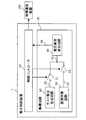
図1は、本実施例における電子制御装置の構成図である。 FIG. 1 is a configuration diagram of an electronic control device according to this embodiment.
電子制御装置1は、制御コントローラ10と集積回路20を備えている。このうち、制御コントローラ10は、内部にCPU(不図示)やRAM(不図示)、通信機能(不図示)を備え、集積回路20に対して処理の指示を行う他に、故障通知装置100に対する故障検出信号の出力や他の電子制御装置との通信を実施する。なお、図1において制御コントローラ10は集積回路20の外部に記されているが、集積回路20の内部にあってもよい。 The
集積回路20は、1チップ内に、監視対象回路30、電圧異常検出回路40、テスト電圧生成回路50、スイッチ21およびスイッチ22を備えている。スイッチ21およびスイッチ22は、制御コントローラ10からの信号により開閉制御される。 The
監視対象回路30は、電圧異常検出回路40が電圧異常を測定する対象となる回路である。監視対象回路30は任意のアナログ回路であり、例えば、電圧昇圧回路や電圧降圧回路、電子制御装置1外部のセンサ電圧を取得する回路などが具体例として挙げられる。 The
電圧異常検出回路40は、入力側の配線41およびスイッチ21を介してテスト電圧生成回路50と接続されており、配線41およびスイッチ22を介して監視対象回路30と接続されている。そのため、電圧異常検出回路40には、テスト電圧生成回路50が出力するテスト電圧55か監視対象回路30の端子電圧31のどちらかが入力される。 The voltage
そして電圧異常検出回路40は、配線41から入力された入力電圧と予め設定した閾値電圧を比較し、入力電圧が正常範囲内であるかを判断する。入力電圧が正常範囲内から逸脱した場合には、制御コントローラ10に対して電圧異常検出信号46を出力する。 The voltage
テスト電圧生成回路50は、電圧異常検出回路40の故障診断を実施するためのテスト電圧55を生成する。 The test voltage generation circuit 50 generates a
故障通知装置100は、制御コントローラ10からの故障検出信号を受け付け、例えば自動車の搭乗者に故障の発生を通知する。故障の通知方法としては、例えば、ランプを点灯させる、警告音を発生させる、音声で通知するなどの方法が挙げられる。 The
図2は、電圧異常検出回路40の回路構成を表した図である。電圧異常検出回路40は、配線41の入力電圧が閾値電圧より高い場合に電圧異常検出信号46を出力するか、閾値電圧より低い場合に電圧異常検出信号46を出力するかによって回路構成が異なる。なお、本実施例において、電圧異常検出回路40から電圧異常検出信号46が出力された状態とは、電圧異常検出信号46の電圧値がCMOSレベルにおけるHighの範囲内にある状態を指す。 FIG. 2 is a diagram illustrating a circuit configuration of the voltage
図2(a)は、配線41の入力電圧が閾値電圧より高い場合に電圧異常検出信号46を出力する電圧異常検出回路40を示している。図2(a)では、配線41の入力電圧を抵抗42aおよび抵抗43aによって分圧し、分圧した入力電圧をコンパレータ44aの非反転入力端子(+側)に入力し、基準電圧45aをコンパレータ44aの反転入力端子(−側)に入力している。これにより、分圧した入力電圧が基準電圧45aより大きい場合には、コンパレータ44aの出力電圧は電源電圧となり、電圧異常検出信号46が出力されている状態となる。逆に、分圧した入力電圧が基準電圧45aより小さい場合には、コンパレータ44aの出力電圧は0Vとなり、電圧異常検出信号46が出力されていない状態となる。この回路の場合、閾値電圧は抵抗42a、抵抗43a、基準電圧45aの値によって決まる。 FIG. 2A shows a voltage
図2(b)は、配線41の入力電圧が閾値電圧より低い場合に電圧異常検出信号46を出力する電圧異常検出回路40である。図2(b)では、配線41の入力電圧を抵抗42bおよび抵抗43bによって分圧し、分圧した入力電圧をコンパレータ44bの反転入力端子(−側)に入力し、基準電圧45bをコンパレータ44bの非反転入力端子(+側)に入力している。これにより、分圧した入力電圧が基準電圧45bより小さい場合には、コンパレータ44bの出力電圧は電源電圧となり、電圧異常検出信号46が出力された状態となる。逆に、分圧した入力電圧が基準電圧45bより大きい場合には、コンパレータ44bの出力は0Vとなり、電圧異常検出信号46は出力されていない状態となる。この回路の場合、閾値電圧は抵抗42b、抵抗43b、基準電圧45bの値によって決まる。 FIG. 2B shows a voltage
図3は、テスト電圧生成回路50の回路構成を表した図である。テスト電圧55は、電源線53の電圧をMOSFET54、抵抗56、抵抗57で分圧して作られ、MOSFET54および抵抗56の共通接続点から出力される。オペアンプ52は、非反転入力端子(+側)の基準電圧51と、反転入力端子(−側)の抵抗56および57の共通接続点電圧58が等しくなるようにMOSFET54の抵抗値を調整する役割があり、これによりMOSFET54および抵抗56の共通接続点から出力されるテスト電圧55の電圧値が安定する仕組みとなっている。 FIG. 3 is a diagram illustrating a circuit configuration of the test voltage generation circuit 50. The
図4は、本実施例における故障診断方法のフローチャートである。 FIG. 4 is a flowchart of the failure diagnosis method in this embodiment.
ステップS1において、制御コントローラ10はスイッチ22が開路(OFF)となるようにOFF制御信号を出力する。これにより、電圧異常検出回路40と監視対象回路30との接続が切断されることになる。次いでステップS2において、制御コントローラ10はスイッチ21が閉路(ON)となるようにON制御信号を出力する。これにより、テスト電圧生成回路50から出力されるテスト電圧55が電圧異常検出回路40に入力されることになる。 In step S1, the
次のステップS3において、制御コントローラ10は電圧異常検出回路40から電圧異常検出信号46が出力されるかを確認する。制御コントローラ10が電圧異常検出信号46を受け取った場合(Yes)は、電圧異常検出回路40は正常であると判断し、ステップS4の処理に移る。電圧異常検出信号46を受け取らなかった場合(No)は、電圧異常検出回路40が故障していると判断し、ステップS6の処理に移る。 In the next step S <b> 3, the
ステップS4では、制御コントローラ10はスイッチ21が開路(OFF)となるようにOFF制御信号を出力する。これにより、テスト電圧生成回路50と電圧異常検出回路40の接続が切断される。次のステップS5では、制御コントローラ10はスイッチ22が閉路(ON)となるようにON制御信号を出力する。これにより、故障診断前と同様に、監視対象回路30の端子電圧31が電圧異常検出回路40に入力されることになる。ステップS5の処理が完了すると、電圧異常検出回路40の故障診断処理は終了となる。 In step S4, the
ステップS6では、制御コントローラ10は故障通知装置100に対して故障検出信号を出力する。これを受けて、故障通知装置100が動作し、搭乗者に故障を通知する。 In step S <b> 6, the
これによって、電圧異常検出回路40の故障を電子制御装置の外部へ通知することができる。 Thereby, the failure of the voltage
ステップS6の処理が完了すると、電圧異常検出回路40の故障診断処理は終了となる。 When the process of step S6 is completed, the fault diagnosis process of the voltage
なお、電圧異常検出回路40の故障診断を開始するタイミングについては任意であり、例えば、電子制御装置1に電源が供給された際に診断を行っても良いし、電子制御装置1が一定時間動作する毎に診断を行っても良い。 The timing for starting the failure diagnosis of the voltage
図5は、テスト電圧55の温度係数と電圧異常検出回路40が持つ閾値電圧の温度係数の関係を表した図である。なお、図5は電圧異常検出回路40として図2(a)の回路を用いた場合の図である。 FIG. 5 is a diagram showing the relationship between the temperature coefficient of the
電圧異常検出回路40として図2(a)の回路を用いた場合、全温度領域においてテスト電圧55は閾値電圧よりも大きい必要がある。これは、テスト電圧55が閾値電圧を下回ると、故障診断時に電圧異常検出回路40から電圧異常検出信号46が出力されず、電圧異常検出回路40が故障していると誤検出されてしまうためである。 When the circuit of FIG. 2A is used as the voltage
この誤検出の問題は、図5(a)のようにテスト電圧55の変動範囲と閾値電圧の変動範囲が重ならないようにすることで、確実に避けることができる。しかし、変動範囲が重ならないようにする場合、テスト電圧55の変動量が大きいと、図5(b)のようにテスト電圧55と閾値電圧の電位差が大きくなる。テスト電圧55と閾値電圧の電位差が大きいほど、電圧異常検出回路40の閾値電圧が上昇するような故障を検出することは困難となる。 This problem of erroneous detection can be reliably avoided by preventing the fluctuation range of the
これに対し、図5(c)のようにテスト電圧55の温度係数と閾値電圧の温度係数をできる限り等しくすることで上記の問題を解決できる。テスト電圧55の温度係数と閾値電圧の温度係数が等しい場合、温度が変化してもテスト電圧55と閾値電圧の電位差は変動しない。そのため、テスト電圧55を閾値電圧の付近に設定しても故障の誤検出が起こることはなく、誤検出を防止しつつ故障検出精度を向上させることができる。テスト電圧55の温度係数と閾値電圧の温度係数の差が小さいほど、この効果は大きくなる。 On the other hand, the above problem can be solved by making the temperature coefficient of the
また、電圧異常検知回路40が図2(b)の回路の場合でも、テスト電圧55と閾値電圧の大小関係が逆転する以外は図2(a)の回路と同じであるため、テスト電圧55の温度係数と閾値電圧の温度係数の差が小さいほど、同じように故障検知精度は向上する。 2B is the same as the circuit of FIG. 2A except that the magnitude relationship between the
テスト電圧55と閾値電圧の温度係数を合わせる方法としては、温度係数が合うように電圧異常検出回路40とテスト電圧生成回路50を設計することと、電圧異常検出回路40とテスト電圧生成回路50にコモンセントロイド配置を適用することが挙げられる。 As a method of matching the temperature coefficient of the
前記設計により温度係数を合わせる方法は、例えば電圧異常検出回路を構成する図2(a)又は図2(b)の抵抗、コンパレータの温度係数と、テスト電圧生成回路を構成する図3の抵抗、コンパレータ、MOSFETの温度係数とをシミュレーションして両者が等しくなるように設計するものである。 The method of adjusting the temperature coefficient according to the design includes, for example, the resistance of FIG. 2A or 2B configuring the voltage abnormality detection circuit, the temperature coefficient of the comparator, and the resistance of FIG. 3 configuring the test voltage generation circuit, The temperature coefficients of the comparator and MOSFET are simulated and designed to be equal.
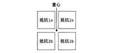
図6はコモンセントロイド配置図の例を示している。コモンセントロイド配置とは、中央に重心が来るように素子を配置する方法である。図6の場合、抵抗1を抵抗1aと抵抗1bの2つに分割し、分割した抵抗1aと抵抗1bを対角に配置している。同様に、抵抗2も抵抗2aと抵抗2bに分割した後に、対角に配置している。これにより、抵抗1a、抵抗1b、抵抗2a、抵抗2bの抵抗値がそれぞれ同じ場合には、重心が中央に来ることになる。コモンセントロイド配置を用いた場合、素子を単純に並べた場合と比べて、集積回路20製造時に重心がばらついて特定の素子に偏ることを防止でき、テスト電圧55の温度係数と閾値電圧の温度係数とのずれを小さくすることができる。 FIG. 6 shows an example of a common centroid layout diagram. The common centroid arrangement is a method of arranging elements so that the center of gravity comes to the center. In the case of FIG. 6, the
例えば電圧異常検出回路40であれば、図2(a)の各抵抗42a,43aを各々2つに分割した後に図6のように対角配置する。尚、抵抗に限らずコンパレータ44aについても2つに分割した後に対角配置してもよい。また図2(b)の回路の場合も同様である。 For example, in the case of the voltage
また、テスト電圧生成回路50であれば、図3の各抵抗56、57を各々2つに分割した後に図6のように対角配置する。尚、抵抗に限らずオペアンプ52、MOSFET54についても2つに分割した後に対角配置してもよい。 Further, in the case of the test voltage generation circuit 50, each of the
以上で説明した実施例1では次のような効果がある。 The first embodiment described above has the following effects.
テスト電圧55の温度係数を電圧異常検出回路40が持つ閾値電圧の温度係数に近づけることで、テスト電圧55を閾値電圧付近に設定することが可能となり、テスト電圧55の電圧変動が大きい場合でも電圧異常検出回路40の故障を精度良く診断することができる。 By bringing the temperature coefficient of the
本実施例では、集積回路の外部からテスト電圧の温度係数調整を可能とする電子制御装置の例を示す。 In the present embodiment, an example of an electronic control device capable of adjusting the temperature coefficient of the test voltage from the outside of the integrated circuit is shown.
図7は、実施例2における電子制御装置1Aの構成図である。ここで、実施例1における電子制御装置1の構成図と同一の要素には同一の記号を付与しており、これら同一の要素に対する説明は省略する。 FIG. 7 is a configuration diagram of the
実施例2における電子制御装置1Aは、実施例1における集積回路20とは異なる集積回路20Aを有している。それ以外は、実施例1の電子制御装置1と同様の構成となっている。 The
実施例2における集積回路20Aは、端子23、端子24を有していることと、実施例1におけるテスト電圧生成回路50とは異なるテスト電圧生成回路50Aを有していること以外は、実施例1における集積回路20と同様の構成となっている。ここで端子23は、テスト電圧生成回路50Aから出力されるテスト電圧55が印加されるように接続されており、これにより、端子23を用いて集積回路20Aの外部からテスト電圧55の温度係数を測定することができる。端子24は、テスト電圧55の温度係数調整用としてテスト電圧生成回路50Aの内部に接続されている。 The
図8は、実施例2におけるテスト電圧生成回路50Aの構成図である。実施例2におけるテスト電圧生成回路50Aは、実施例1におけるテスト電圧生成回路50に加えて、抵抗57に並列接続される、調整抵抗59およびツェナーダイオード60の直列回路を有している。また、調整抵抗59およびツェナーダイオード60の共通接続点が端子24と接続されている点も異なる。 FIG. 8 is a configuration diagram of the test voltage generation circuit 50A in the second embodiment. In addition to the test voltage generation circuit 50 in the first embodiment, the test voltage generation circuit 50A in the second embodiment includes a series circuit of an
この端子24は、テスト電圧55の温度係数を調整する際に使用する。端子24に高電圧を印加すると、ツェナーダイオード60のアノード、カソード間がショート状態となる。これにより、抵抗57と調整抵抗59が並列接続され、テスト電圧55の温度係数を変化させることができる。 This terminal 24 is used when adjusting the temperature coefficient of the
この際、テスト電圧を変更させない場合には、抵抗57に並列接続される調整抵抗59の抵抗値は、抵抗57の抵抗値よりも十分に小さいものとする。 At this time, when the test voltage is not changed, the resistance value of the
なお、実施例2では、温度係数を調整するための端子24、調整抵抗59、ツェナーダイオード60(本発明のテスト電圧の温度係数を調整する手段)を1つずつしか用いていないが、実際には複数の端子と調整抵抗を用いても良い。また、別の方法、例えば、テスト電圧生成回路50A内の抵抗にレーザーで切れ目を入れて抵抗値を変化させ、テスト電圧55の温度係数を調整しても良い。 In the second embodiment, the terminal 24 for adjusting the temperature coefficient, the
以上で説明した実施例2では次のような効果がある。 The second embodiment described above has the following effects.
電子制御装置1Aにおける集積回路20Aは、テスト電圧55を出力可能な端子23を有することで、集積回路20Aの外部からテスト電圧55の電圧値を検出し、その温度係数を測定することができる。テスト電圧55を測定した結果、温度係数にずれが生じている場合には、端子24を利用してテスト電圧55の温度係数を調整することができる。 The
また、他の実施形態としては、前記テスト電圧の温度係数を測定するための端子23と、テスト電圧の温度係数を調整する手段(端子24、調整抵抗59、ツェナーダイオード60)は、どちらか一方のみを設ける構成にしてもよい。 In another embodiment, one of the terminal 23 for measuring the temperature coefficient of the test voltage and the means for adjusting the temperature coefficient of the test voltage (
本実施例では、電圧異常検出回路の閾値電圧が集積回路の電源電圧よりも高い場合でも、電圧昇圧回路なしに電圧異常検出回路の故障診断を実施できる電子制御装置の例を示す。 In the present embodiment, an example of an electronic control device capable of performing failure diagnosis of the voltage abnormality detection circuit without the voltage booster circuit even when the threshold voltage of the voltage abnormality detection circuit is higher than the power supply voltage of the integrated circuit is shown.
図9は、実施例3における電子制御装置の構成図である。ここで、実施例1における電子制御装置の構成図と同一の要素には同一の記号を付与しており、これら同一の要素に対する説明は省略する。 FIG. 9 is a configuration diagram of an electronic control device according to the third embodiment. Here, the same symbols are assigned to the same elements as those in the configuration diagram of the electronic control device according to the first embodiment, and the description for these same elements is omitted.
実施例3における電子制御装置1Bは、実施例1における集積回路20とは異なる集積回路20Bを有している。それ以外は、実施例1の電子制御装置1と同様の構成となっている。 The
実施例3における集積回路20Bは、実施例1における電圧異常検出回路40とは異なる電圧異常検出回路40Bを有していることが異なる。また、実施例3では、実施例1とは異なり、監視対象回路30の端子電圧31はスイッチ22および配線41を介して電圧異常検出回路40Bに入力され、テスト電圧生成回路50から出力されたテスト電圧55は、スイッチ21、および配線41とは別の配線47を介して電圧異常検出回路40Bに入力される構成となっている。 The
図10は、実施例3における電圧異常検出回路40Bの構成図である。電圧異常検出回路40Bでは、テスト電圧生成回路50からのテスト電圧55が、図10(a)のように配線47を通して抵抗42aと抵抗43aの間に入力されるか、又は図10(b)のように配線47を通して抵抗42bと抵抗43bの間に入力される以外は、実施例1における電圧異常検出回路40と同様である。 FIG. 10 is a configuration diagram of the voltage
図10(a)は、抵抗42aおよび43aの共通接続点電圧が閾値電圧より高い場合に電圧異常検出信号46を出力する電圧異常検出回路40Bを示している。図10(a)では、監視対象回路30から配線41を通して導入される入力電圧を抵抗42aおよび抵抗43aによって分圧し、抵抗42aおよび43aの共通接続点(分圧点)を、テスト電圧生成回路50から配線47を通して導入されるテスト電圧の入力端子とし、前記分圧点の電圧をコンパレータ44aの非反転入力端子(+側)に入力し、基準電圧45aをコンパレータ44aの反転入力端子(−側)に入力している。これにより、配線47を通して導入されるテスト電圧か、又は配線41を通して導入され抵抗42a,43aにより分圧された入力電圧が基準電圧45aより大きい場合には、コンパレータ44aの出力電圧は電源電圧となり、電圧異常検出信号46が出力されている状態となる。逆に、配線47を通して導入されるテスト電圧か、又は配線41を通して導入され抵抗42a,43aにより分圧された入力電圧が基準電圧45aより小さい場合には、コンパレータ44aの出力電圧は0Vとなり、電圧異常検出信号46が出力されていない状態となる。 FIG. 10A shows a voltage
図10(b)は、抵抗42bおよび43bの共通接続点電圧が閾値電圧より低い場合に電圧異常検出信号46を出力する電圧異常検出回路40Bである。図10(b)では、監視対象回路30から配線41を通して導入される入力電圧を抵抗42bおよび抵抗43bによって分圧し、抵抗42bおよび43bの共通接続点(分圧点)を、テスト電圧生成回路50から配線47を通して導入されるテスト電圧の入力端子とし、前記分圧点の電圧をコンパレータ44bの反転入力端子(−側)に入力し、基準電圧45bをコンパレータ44bの非反転入力端子(+側)に入力している。これにより、配線47を通して導入されるテスト電圧か、又は配線41を通して導入され抵抗42b,43bにより分圧された入力電圧が基準電圧45bより小さい場合には、コンパレータ44bの出力電圧は電源電圧となり、電圧異常検出信号46が出力された状態となる。逆に、配線47を通して導入されるテスト電圧か、又は配線41を通して導入され抵抗42b,43bにより分圧された入力電圧が基準電圧45bより大きい場合には、コンパレータ44bの出力は0Vとなり、電圧異常検出信号46は出力されていない状態となる。 FIG. 10B shows a voltage
実施例1で説明したテスト電圧生成回路50では、電源電圧を分圧してテスト電圧を生成している。そのため、電圧異常検出回路40の閾値電圧が電源電圧よりも高い場合には、電源電圧よりも高いテスト電圧を生成するために、テスト電圧生成回路50内に電圧昇圧回路を加える必要がある。しかし、電圧昇圧回路を追加すると、集積回路20の回路面積が増加し、コスト増につながる。 In the test voltage generation circuit 50 described in the first embodiment, the test voltage is generated by dividing the power supply voltage. Therefore, when the threshold voltage of the voltage
この問題を解決するため、実施例3における電圧異常検出回路40Bでは、分圧用抵抗の間(抵抗42aおよび43aの共通接続点(図10(a))、又は抵抗42bおよび43bの共通接続点(図10(b)))に、配線47を介してテスト電圧を入力する構成としている。この構成の場合、抵抗42aおよび43aの共通接続点(又は抵抗42bおよび43bの共通接続点)に導入されたテスト電圧が閾値電圧と比較されるため、配線41を介して入力する場合よりもテスト電圧を低くすることができ、前記電圧昇圧回路を不要にすることができる。以上が実施例3における効果である。 In order to solve this problem, in the voltage
本実施例では、監視対象回路もしくは電圧異常検出回路の故障が検出された際に、故障部分の特定を容易にすることができる電子制御装置の例を示す。 In the present embodiment, an example of an electronic control device capable of facilitating identification of a faulty part when a fault of a monitoring target circuit or a voltage abnormality detection circuit is detected will be described.
図11は、実施例4における電子制御装置の構成図である。ここで、実施例1における電子制御装置の構成図と同一の要素には同一の記号を付与おり、これら同一の要素に対する説明は省略する。 FIG. 11 is a configuration diagram of an electronic control device according to the fourth embodiment. Here, the same symbols are assigned to the same elements as those in the configuration diagram of the electronic control device according to the first embodiment, and descriptions of these same elements are omitted.
実施例4における電子制御装置1Cは、実施例1における制御コントローラ10とは異なる制御コントローラ10Cを有している。それ以外は、実施例1の電子制御装置1と同様の構成となっている。 The
実施例4における制御コントローラ10Cは、実施例1における制御コントローラ10に加えて、故障情報11を有している。 The
図12は、故障情報11の例を表した図である。故障情報11は、故障番号11a、日付11b、時間11c、故障コード11dを有している。故障番号11aは、故障の登録番号であり、図12の場合には最大N個の情報を保持できる。 日付11bおよび時間11cは、故障が発生した日時を示している。故障コード11dの部分には、検出された故障内容によって異なるコードが保存される。例えば、監視対象回路30の端子電圧が異常となった場合にはC00、電圧異常検出回路40の故障診断時に異常が検出された場合にはC01のコードが保存される。 FIG. 12 is a diagram illustrating an example of the
この故障情報11は、制御コントローラ10Cにより電子制御装置1C外部から読み出しおよび消去の操作が可能である。 The
以上で説明した実施例4では次のような効果がある。 The fourth embodiment described above has the following effects.
電子制御装置1Cにおける制御コントローラ10Cは、故障検出時の故障内容を故障情報11として保持する。故障発生時には、この故障情報11を電子制御装置1C外部から読み出すことで、故障発生の時間や故障部分の特定が容易となる。 The
なお、本発明は上記の実施例に限定されるものではなく、さまざまな変形例が含まれる。例えば、上記した実施例は本発明を分かりやすく説明するために詳細に説明したものであり、必ずしも説明した全ての構成を備えるものに限定されるものではない。 In addition, this invention is not limited to said Example, Various modifications are included. For example, the above-described embodiments have been described in detail for easy understanding of the present invention, and are not necessarily limited to those having all the configurations described.
また、上記の各構成、機能、処理部、処理手段等は、それらの一部または全部を、例えば集積回路で設計する等によるハードウェアで実現してもよい。また、上記の各構成、機能等は、プロセッサがそれぞれの機能を実現するプログラムを解釈し、実行することによるソフトウェアで実現してもよい。 Each of the above-described configurations, functions, processing units, processing means, and the like may be realized by hardware by designing a part or all of them with, for example, an integrated circuit. In addition, each of the above-described configurations, functions, and the like may be realized by software obtained by the processor interpreting and executing a program that realizes each function.
また、制御線や情報線は説明上必要と考えられるものを示しており、製品上必ずしも全ての制御線や情報線を示しているとは限らない。実際には、殆ど全ての構成が相互に接続されていると考えて良い。 Further, the control lines and information lines indicate what is considered necessary for the explanation, and not all the control lines and information lines on the product are necessarily shown. In practice, it can be considered that almost all the components are connected to each other.
1,1A,1B,1C…電子制御装置
10,10C…制御コントローラ
20,20A,20B…集積回路
30…監視対象回路
40,40B…電圧異常検出回路
41,47…配線
42a,42b,43a,43b,56,57…抵抗
44a,44b…コンパレータ
50,50A…テスト電圧生成回路
52…オペアンプ
54…MOSFET
59…調整抵抗
100…故障通知装置DESCRIPTION OF
59 ...
Claims (7)
Translated fromJapanese前記テスト電圧の温度係数と前記閾値電圧の温度係数を等しくなるように設定したことを特徴とする電子制御装置。A monitoring target circuit provided in an integrated circuit composed of one chip, a voltage abnormality detection circuit that detects an abnormality of the monitoring target circuit by comparing a terminal voltage of the monitoring target circuit with a preset threshold voltage; A test voltage generation circuit that generates a test voltage that is preset to detect a failure of the voltage abnormality detection circuit and is compared with a threshold voltage of the voltage abnormality detection circuit;
An electronic control device, wherein the temperature coefficient of the test voltage and the temperature coefficient of the threshold voltage are set to be equal.
前記集積回路との間で信号の授受を行う制御コントローラを有し、該制御コントローラは、前記電圧異常検出回路の故障が検出されたときに故障検出信号を外部に出力することを特徴とする電子制御装置。The electronic control device according to claim 1.
An electronic device comprising: a controller that exchanges signals with the integrated circuit, wherein the controller outputs a failure detection signal to the outside when a failure of the voltage abnormality detection circuit is detected. Control device.
前記テスト電圧生成回路と電圧異常検出回路をコモンセントロイド配置して、前記テスト電圧の温度係数と前記閾値電圧の温度係数を等しくなるように設定したことを特徴とする電子制御装置。The electronic control device according to claim 1 or 2,
An electronic control device, wherein the test voltage generation circuit and the voltage abnormality detection circuit are arranged in a common centroid and the temperature coefficient of the test voltage and the temperature coefficient of the threshold voltage are set to be equal.
前記集積回路は、前記テスト電圧を集積回路の外部に出力する端子を有することを特徴とする電子制御装置。The electronic control device according to any one of claims 1 to 3,
The electronic control device, wherein the integrated circuit has a terminal for outputting the test voltage to the outside of the integrated circuit.
前記集積回路は、前記テスト電圧の温度係数を調整する手段を有することを特徴とする電子制御装置。The electronic control device according to any one of claims 1 to 4,
The electronic control device, wherein the integrated circuit has means for adjusting a temperature coefficient of the test voltage.
前記電圧異常検出回路は、前記テスト電圧の入力端子を分圧抵抗の分圧点に有することを特徴とする電子制御装置。The electronic control device according to any one of claims 1 to 5,
The electronic controller according to claim 1, wherein the voltage abnormality detection circuit has an input terminal for the test voltage at a voltage dividing point of a voltage dividing resistor.
前記制御コントローラは、前記電圧異常検出回路からの故障情報を保持する機能を有していることを特徴とする電子制御装置。The electronic control device according to any one of claims 2 to 6,
The electronic controller according to claim 1, wherein the controller has a function of holding failure information from the voltage abnormality detection circuit.
Priority Applications (2)
| Application Number | Priority Date | Filing Date | Title |
|---|---|---|---|
| JP2012264893AJP5830458B2 (en) | 2012-12-04 | 2012-12-04 | Electronic control unit |
| PCT/JP2013/081515WO2014087854A1 (en) | 2012-12-04 | 2013-11-22 | Electronic control apparatus |
Applications Claiming Priority (1)
| Application Number | Priority Date | Filing Date | Title |
|---|---|---|---|
| JP2012264893AJP5830458B2 (en) | 2012-12-04 | 2012-12-04 | Electronic control unit |
Publications (2)
| Publication Number | Publication Date |
|---|---|
| JP2014110361A JP2014110361A (en) | 2014-06-12 |
| JP5830458B2true JP5830458B2 (en) | 2015-12-09 |
Family
ID=50883277
Family Applications (1)
| Application Number | Title | Priority Date | Filing Date |
|---|---|---|---|
| JP2012264893AExpired - Fee RelatedJP5830458B2 (en) | 2012-12-04 | 2012-12-04 | Electronic control unit |
Country Status (2)
| Country | Link |
|---|---|
| JP (1) | JP5830458B2 (en) |
| WO (1) | WO2014087854A1 (en) |
Families Citing this family (4)
| Publication number | Priority date | Publication date | Assignee | Title |
|---|---|---|---|---|
| WO2015033708A1 (en)* | 2014-07-30 | 2015-03-12 | 株式会社小松製作所 | Utility vehicle, and control method for utility vehicle |
| JP6735611B2 (en)* | 2016-06-17 | 2020-08-05 | ローム株式会社 | Electronic circuits, electronic devices and integrated circuits |
| JP6729323B2 (en)* | 2016-11-24 | 2020-07-22 | トヨタ自動車株式会社 | Anomaly judgment device |
| CH721532A1 (en)* | 2024-01-23 | 2025-07-31 | Elesta Gmbh | Overvoltage and/or undervoltage testing |
Family Cites Families (3)
| Publication number | Priority date | Publication date | Assignee | Title |
|---|---|---|---|---|
| JPS62123923A (en)* | 1985-11-20 | 1987-06-05 | 日本電信電話株式会社 | Monitoring circuit for secondary battery power supply |
| JPS62123924A (en)* | 1985-11-20 | 1987-06-05 | 日本電信電話株式会社 | Secondary battery deterioration determination circuit |
| JP4715875B2 (en)* | 2008-06-25 | 2011-07-06 | トヨタ自動車株式会社 | Failure diagnosis method for voltage abnormality detection means, secondary battery system, and hybrid vehicle |
- 2012
- 2012-12-04JPJP2012264893Apatent/JP5830458B2/ennot_activeExpired - Fee Related
- 2013
- 2013-11-22WOPCT/JP2013/081515patent/WO2014087854A1/enactiveApplication Filing
Also Published As
| Publication number | Publication date |
|---|---|
| JP2014110361A (en) | 2014-06-12 |
| WO2014087854A1 (en) | 2014-06-12 |
Similar Documents
| Publication | Publication Date | Title |
|---|---|---|
| CN109477862B (en) | Vehicle control device | |
| JP5830458B2 (en) | Electronic control unit | |
| US9520830B2 (en) | Crystal oscillator | |
| CN110832329B (en) | Device and method for checking the functional validity of a system resistor of a battery system | |
| KR20150053273A (en) | Method and device for checking the plausibility of a current sensor measurement result | |
| CN101825651A (en) | Probe card, semiconductor test device including probe card, and fuse inspection method for probe card | |
| US8698353B2 (en) | Method for operating a redundant system and system therefor | |
| US11079409B2 (en) | Assembly with at least two redundant analog input units for a measurement current | |
| JP5312316B2 (en) | Switch status detection device | |
| US20170363481A1 (en) | Fault Detection Apparatus | |
| JP2009532835A5 (en) | ||
| EP3985826A1 (en) | Battery protection and verification system | |
| JP6225486B2 (en) | Cell voltage measuring device | |
| US10915387B2 (en) | Circuit assembly and method for monitoring a micro-controller based on a watchdog voltage | |
| CN106574945A (en) | Detection of dependent failures | |
| US10746610B2 (en) | Safety circuit, a safety circuit operation method and an electrically operated motor comprising a safety circuit | |
| CN210922684U (en) | Power-on aging test circuit based on temperature and humidity sensor, PCB and device thereof | |
| EP2701028B1 (en) | An integrated circuit with an external reference resistor network | |
| EP2239588B1 (en) | Voltage surveillance circuit | |
| EP2182604A1 (en) | Electrical power supply monitoring apparatus | |
| US20170256341A1 (en) | Control circuit and control method | |
| JP2011061968A (en) | Power supply monitoring circuit, power supply monitoring method used for the same, power supply monitoring control program, and electronic apparatus | |
| JP2008102094A (en) | Voltage monitoring method and apparatus | |
| JP6038529B2 (en) | measuring device | |
| JP2015021954A (en) | Current controller |
Legal Events
| Date | Code | Title | Description |
|---|---|---|---|
| A621 | Written request for application examination | Free format text:JAPANESE INTERMEDIATE CODE: A621 Effective date:20150226 | |
| TRDD | Decision of grant or rejection written | ||
| A01 | Written decision to grant a patent or to grant a registration (utility model) | Free format text:JAPANESE INTERMEDIATE CODE: A01 Effective date:20150929 | |
| A61 | First payment of annual fees (during grant procedure) | Free format text:JAPANESE INTERMEDIATE CODE: A61 Effective date:20151026 | |
| R150 | Certificate of patent or registration of utility model | Ref document number:5830458 Country of ref document:JP Free format text:JAPANESE INTERMEDIATE CODE: R150 | |
| LAPS | Cancellation because of no payment of annual fees |